voltage compensation and power factor correction in
TRANSCRIPT

Voltage Compensation and Power Factor Correction in Distribution Networks with DVR
N.M. Salgado-Herrera, A. Medina-Ríos, R. Tapia-Sánchez
Facultad de Ingeniería Eléctrica, División de Estudios de Posgrado,
UMSNH Morelia, CP 58030, México.
E-mails: [email protected], [email protected],
O. Anaya-Lara Department of Electronic and
Electrical Engineering, Institute for Energy and
Environment, University of Strathclyde, Glasgow, G1 1XW, U.K E-mail: [email protected]
J.R. Rodríguez-Rodríguez Facultad de Ingeniería Eléctrica,
División de Estudios de Posgrado, Instituto Tecnológico de Morelia
Morelia, CP 58120, México. E-mail: [email protected]
Abstract—The stability analysis and voltage regulation in distribution systems, as well as power quality problems such as voltage sags, swells, due to connection and disconnection of large loads, short circuits and the presence of non-linear loads, require of the consideration of adequate technical solutions. In this paper, a Dynamic Voltage Restorer (DVR) model based on a power converter scheme for voltage compensation due to the presence of sags of amplitude since 0.1pu to 0.9pu and swells with amplitude from 1.1pu to 1.9pu, and power factor correction in distribution networks is proposed. The results are verified through MATLAB & Simulink.
Keywords— DVR; power factor; sags; swells; distribution networks; power converter.
I. INTRODUCTION
IT is clear that at present, the user that does usage of power is increasingly dependent on technology, for example in areas such as industry and medicine, where sensitive equipment to energy abrupt changes, damaged by poor voltage quality can cause large monetary losses, reduction of the devices lifespan, sensible harm to user´s health or even death. To avoid such anomalies the power network operation under the proper voltage regulation and stability is required. Voltage sags in power networks are not always possible to prevent due to the finite time compensation of faults that cause voltage drops to spread to sensitive loads in distribution systems [1].
Dynamic Voltage Restorer (DVR) is a custom power device based on a power converter which is becoming increasingly popular in power system applications for voltage sags and swells compensation [2], to improve voltage stability, network failure recovery, to mitigate voltage flicker, security of load [3], damping of system oscillations and to improve generation system transient and dynamic stability in the system [4], [5]. The DVR is connected in series to the grid through a transformer; it is placed on the distribution system between the supply and the feeder critical load at the point of common coupling (PCC) [6]. Westinghouse for the Electric Power Research Institute (EPRI) built the first DVR in the U.S., and it was installed in 1996 on the Duke Power Company grid system
to protect an automated yarn manufacturing and weaving factory [7]. A DVR can be manipulated by different control strategies; for example, in [1] a DVR without energy storage elements is described. Thus, the overall size of the DVR is reduced. However, since it has no energy storage elements, it is not capable of compensating deep sags or pronounced swells. In [4] a DVR able to compensate for sags in a range of 0.16pu to 0.5pu is described, but it is not capable of correcting power factor. In [8] a DVR model for power factor correction based on an optimal control strategy is proposed.
This research work reports findings on the representation and results obtained from the DVR application for voltage compensation on sags of amplitude since 0.1pu to 0.9pu and swells with amplitude from 1.1pu to 1.9pu, as well as power factor correction in power networks.
II. CHARACTERISTICS AND MODELING OF DVR IN THE DISTRIBUTION NETWORK
The DVR based on a Voltage Source Converter (VSC) operation generates AC voltages through the IGBTs switching [9]. A DVR produces a voltage, which can be continuously or gradually adjusted by the distribution line compensation. The 6-pulse three-phase is the most common arrangement. At DC converter terminals, a parallel capacitor is connected to simulate a voltage source; its purpose is to serve as energy storage for the power flow control. The phase current is flowing through the AC circuit, with respect to VSC voltage terminals. It determines if the VSC is operating as a rectifier or as an inverter, that is, by delivering or absorbing energy from the AC network. The PCC is the node where the VSC and the generating source are connected.
In this research, particular reference is made to the presence of voltage sags and swells. The case study to be described starts from initial conditions, with the system operating in steady state. Nominal operation data of DVR are 3MVA of base power with an input voltage Vs = 2.5kV and a frequency of 60Hz. DVR connection is made between two distribution lines;

of 25km and 1km, respectively, through a series load connection RL and a transformer with a turn ratio of 1:10, to regulate the voltage at the PCC, as shown by Figure 1.
Figure 1Distribution network with DVR
The DVR parameters are obtained from the base total power used and the input voltage as,
PPCC = 32
VPCC IPCC (1)
From (1) I is obtained as,
IPCC = 23⎛
⎝⎜
⎞
⎠⎟
PPCC
VPCC
= 23
3MVA2500V⎛
⎝⎜
⎞
⎠⎟ = 800A (2)
The system base impedance is:
ZPCC =VPCC
IPCC
= 2500V800A
= 3.125Ω (3)
The inductance value is calculated as,
Labc =ZPCC
ω0
= 3.125Ω2π f
= 3.125Ω2π 60Hz( ) = 8.3x10⁻³ H (4)
The resistance value is chosen in the range of 0.1Ω to 0.5Ω. For this case, the resistance value is 0.2Ω.
III. CONTROL AND MODELING: VOLTAGE COMPENSATION AND POWER FACTOR CORRECTION
Power factor correction is achieved by the line current through the id and iq components, that is, feed-forward and feed backward signals are transformed to dq-frame reference, then processed by compensators, produced by control signals within the same framework. Finally, the control signals are transformed back to abc coordinates, which feeds the VSC. Reference commands idref and iqref are limited by saturation blocks for the VSC protection.
The active power P and power factor θ are obtained from (5) and (6), which are controlled by the voltage amplitude, phase angle at the PCC and the VSC line current, respectively.
PPCCref (t) = 32
VPCCd (t)id (t)⎡⎣ ⎤⎦ (5)
θPCCref (t) = − 32
VPCCd (t)iq (t)⎡⎣ ⎤⎦ (6)
Equations (7) and (8) are introduced in order to have independent control of P and θ, being the dq-frame reference used and assuming steady state operating conditions. P and θ can be manipulated through (9) and (10), that is:
idref (t) = 23
PPCCref (t)VPCCd (t)
⎛
⎝⎜⎜
⎞
⎠⎟⎟ (7)
iqref (t) = − 23
θPCCref (t)VPCCd (t)
⎛
⎝⎜⎜
⎞
⎠⎟⎟ (8)
Ldid
dt
⎛
⎝⎜⎜
⎞
⎠⎟⎟= Lω0iq (t) − Rid (t) +Vtd (t) −VPCCd (t) (9)
Ldiq
dt
⎛
⎝⎜⎜
⎞
⎠⎟⎟ = −Lω0id (t) − Riq (t) +Vtq (t) −VPCCq (t) (10)
Figure 2 shows the VSC control diagram.
Figure 2 VSC control diagram
Finally, the dq compensating process is described by,
ed (t) = idref (t) − id (t) (11)
eq (t) = iqref (t) − iq (t)
(12)
In Figure 2, kd(s) and kq(s) are replaced by a proportional integral compensator PI, given by,
k(s) =k p (s) + ki (s)
s (13)
where kp and ki are the proportional and integral gains, respectively, obtained as,
kp (s) = Lτ i
(14)
ki (s) = Rτ i
(15)
were τi is the closed loop system time constant; usually it is in the range of 0.5-5ms. A value of 5ms has been assumed.
The DVR is capable of providing the necessary reactance when a voltage variation occurs. This means that the DC bus voltage must be kept constant. Figure 3 shows the feedback model used.
Figure 3DC voltage feedback Diagram
The magnitude of the feedback DC voltage and reference DC voltage are squared, since the DC current increases to the square of the DC Voltage.
Figure 4 Schematic of the PCC Voltage Control [10].
Figure 4 shows the control diagram of the PCC voltage, the compensator PI is from VPCCdref – VPCCd generating θPCCref, through a PI control.
IV. RESULTS: VOLTAGE SAGS AND SWELLS COMPENSATION AND POWER FACTOR CORRECTION
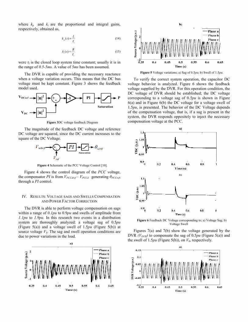
The DVR is able to perform voltage compensation on sags within a range of 0.1pu to 0.9pu and swells of amplitude from 1.1pu to 1.9pu. In this research two events in a distribution system are thoroughly analyzed: a voltage sag of 0.5pu (Figure 5(a)) and a voltage swell of 1.5pu (Figure 5(b)) at source voltage VS. The sag and swell operation conditions are due to power variations in the load.
Figure 5 Voltage variations; a) Sag of 0.5pu; b) Swell of 1.5pu.
To verify the correct system operation, the capacitor DC voltage behavior is analyzed. Figure 6 shows the feedback voltage supplied by the DVR. For this operation condition, the DC voltage of DVR should be established; the DC voltage corresponding to a voltage sag of 0.5pu is shown in Figure 6(a) and in Figure 6(b) the DC voltage for a voltage swell of 1.5pu, is presented. The behavior of the DC Voltage depends of the compensation voltage, that is, if a sag is present in the system, the DVR responds oppositely to inject the necessary compensation voltage at the PCC.
Figure 6 Feedback DC Voltage corresponding to; a) Voltage Sag; b)
Voltage Swell
Figures 7(a) and 7(b) show the voltage generated by the DVR (VDVR) to compensate the sag of 0.5pu (Figure 5(a)) and the swell of 1.5pu (Figure 5(b)), on VS, respectively.
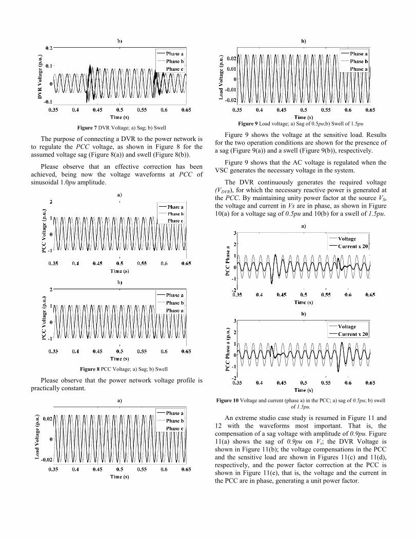
Figure 7 DVR Voltage; a) Sag; b) Swell
The purpose of connecting a DVR to the power network is to regulate the PCC voltage, as shown in Figure 8 for the assumed voltage sag (Figure 8(a)) and swell (Figure 8(b)).
Please observe that an effective correction has been achieved, being now the voltage waveforms at PCC of sinusoidal 1.0pu amplitude.
Figure 8 PCC Voltage; a) Sag; b) Swell
Please observe that the power network voltage profile is practically constant.
Figure 9 Load voltage; a) Sag of 0.5pu;b) Swell of 1.5pu
Figure 9 shows the voltage at the sensitive load. Results for the two operation conditions are shown for the presence of a sag (Figure 9(a)) and a swell (Figure 9(b)), respectively.
Figure 9 shows that the AC voltage is regulated when the VSC generates the necessary voltage in the system.
The DVR continuously generates the required voltage (VDVR), for which the necessary reactive power is generated at the PCC. By maintaining unity power factor at the source VS, the voltage and current in Vs are in phase, as shown in Figure 10(a) for a voltage sag of 0.5pu and 10(b) for a swell of 1.5pu.
Figure 10 Voltage and current (phase a) in the PCC; a) sag of 0.5pu; b) swell
of 1.5pu.
An extreme studio case study is resumed in Figure 11 and 12 with the waveforms most important. That is, the compensation of a sag voltage with amplitude of 0.9pu. Figure 11(a) shows the sag of 0.9pu on Vs; the DVR Voltage is shown in Figure 11(b); the voltage compensations in the PCC and the sensitive load are shown in Figures 11(c) and 11(d), respectively, and the power factor correction at the PCC is shown in Figure 11(e), that is, the voltage and the current in the PCC are in phase, generating a unit power factor.

Figure 11 Waveforms for a sag of 0.9pu; a) Source Voltage Vs; b) DVR
Voltage; c) PCC Voltage; d) Load Voltage; e) Voltage and current in the PCC (phase a) for sag of 0.9pu.
Figure 12 Waveforms for a swell of 1.9pu; a) Source Voltage Vs; b) DVR Voltage; c) PCC Voltage; d) Load Voltage; e) Voltage and current in the PCC
(phase a) for swell of 1.9pu.

Finally, in the Figure 12 the compensation of a swell voltage with amplitude of 1.9pu is presented. Figure 12(a) shows the swell occurs on Vs of 1.9pu; the DVR Voltage is shown in Figure 12(b); the voltage compensations in the PCC in Figures 12(c), the sensitive load voltage are shown and 12(d) and the power factor correction at the PCC with unit power factor is shown in Figure 12(e).
V. CONCLUSIONS
In this contribution, an effective representation and modeling of the power system dynamic operation containing a DVR for sags/swells compensation and power factor correction has been presented.
It has been verified that it is viable and efficient to use a DVR in a distribution network, since it is able to inject the necessary voltage correction in the presence of unbalance and adverse power quality effects, thus improving its stability and power quality.
Simulation results in Matlab/Simulink® demonstrate that the control used in the DVR structure can effectively compensate voltage variations, that is, sags within a range of 0.1pu to 0.9pu and swells with amplitude from 1.1pu to 1.9pu, achieve a load power factor equal to 1, that is, the load voltage and current are in phase.
REFERENCES [1] P. Jayaprakash, B. Singh, D.P. Kothari, A. Chandraand and K. Al-
Haddad, "Control of Reduced-Rating Dynamic Voltage Restorer With a Battery Energy Storage System," Industry Applications, IEEE Transactions on , vol. 50, no.2, pp. 1295,1303, March-April 2014.
[2] I. Pathan Abrarkhan, S S. Vanamane and R.H. Chile, "Different control techniques of Dynamic Voltage Restorer for power quality problems," Automation, Control, Energy and Systems (ACES), 2014 First International Conference on, pp.1,6, 1-2 Feb. 2014.
[3] I. Kasikci, "A new method for power factor correction and harmonic elimination in power systems," Harmonics and Quality of Power, 2000. Proceedings. Ninth International Conference on , vol.3, pp.810,815 vol.3, 2000.
[4] E. Babaei, M.F. Kangarlu and M. Sabahi, "Dynamic voltage restorer based on multilevel inverter with adjustable dc-link voltage," Power Electronics, IET , vol.7, no.3, pp.576,590, March 2014.
[5] Y. Prakash and S. Sankar, "Power quality improvement using DVR in power system," Power and Energy Systems Conference: Towards Sustainable Energy, 2014 , vol., no., pp.1,6, 13-15 March 2014.
[6] V. Jayalakshmiand and N.O. Gunasekar, "Implementation of discrete PWM control scheme on Dynamic Voltage Restorer for the mitigation of voltage sag /swell," Energy Efficient Technologies for Sustainability (ICEETS), 2013 International Conference on , vol., no., pp. 1036,1040, 10-12 April 2013.
[7] A.P. Torres, P. Roncero-Sanchez, X. del Toro Garciaand and V.F. Batlle, "Generalized Proportional-Integral control for voltage-sag compensation in Dynamic Voltage Restorers," Compatibility and Power Electronics (CPE), 2011 7th International Conference-Workshop , vol., no., pp.92,97, 1-3 June 2011.
[8] Wu Fu-Zhuan and Pei Su-ping, "The Research and Implementation of Dynamic Voltage Restorer with Power Factor Correction," Intelligent Systems and Applications (ISA), 2011 3rd International Workshop on , vol., no., pp.1,4, 28-29 May 2011.
[9] K.N.V. Prasad, G.R. Kumar, Y.S.A. Kumarand and G.S. Narayana, "Realization of cascaded H-bridge 5-Level multilevel inverter as Dynamic Voltage Restorer," Computer Communication and Informatics (ICCCI), 2013 International Conference on , vol., no., pp.1,6, 4-6 Jan. 2013.
[10] A. Yazdani and R. Iravani, Voltage-Source Converters in Power Systems: Modeling, Control and Aplications, New Jersey: John Wiley and Son, 2010, pp. 204 – 230. ISBN 978 0 470 52156 4.
BIOGRAPHIES Nadia María Salgado-Herrera Received the B.Eng. And M.Sc. degree
in Electronics Engineering and Electrical Engineering from Instituto Tecnológico de Morelia, Michoacán, México in 2009 and 2011.The research interests include Power electronics, Power Quality and Renewable energy. She is currently working towards her Ph.D. degree in Electrical Engineering at the Universidad Michoacana de San Nicolás de Hidalgo.
Aurelio Medina-Ríos Obtained his Ph.D. from the University of Canterbury, Christchurch, New Zealand in 1992. He has worked as a Post-Doctoral Fellow at the Universities of Canterbury, New Zealand (1 year) and Toronto, Canada (2 years). At present he is a staff member of the Facultad de Ingeniería Eléctrica, UMSNH, Morelia, Mexico where he is the Head of the Division for Posgraduate Studies in Electrical Engineering. His research interests are in the dynamic and steady state analysis is of power systems.
Roberto Tapia-Sánchez He received his PhD from Ecole Centrale de Lille, Lille, France in 2011. He joined the Faculty of Electrical Engineering at the University of Michoacán, Morelia, Mexico in 2011, where he is currently professor in the Division of Graduate Studies. His research interest focuses on the design and control of renewable energy systems.
Olimpo Anaya-Lara (M’98) received the B.Eng. and M.Sc. degrees from the Instituto Tecnológico de Morelia, Morelia, Mexico, in 1990 and 1998, respec- tively, and the Ph.D. degree from the University of Glasgow, Glasgow, U.K., in 2003. His industrial experience includes periods with Nissan Mexicana, Toluca, Mexico, and Construcción y Servicios del Golfo (CSG) Consultants, Coatzacoalcos, Mexico. He is currently on secondment as a Det Norske Veritas Visiting Professor with the Norwegian Research Centre for Offshore Wind Technology, Trondheim, Norway, from his normal position as a Senior Lecturer with the Institute for Energy and Environment, Department of Electronic and Electrical Engineering, University of Strathclyde, Glasgow. His current research interests include wind generation, power electronics, and stability of mixed generation power systems.
Juan Ramón Rodríguez-Rodríguez Received the B.Eng. degree in Electronics Engineering and Ph.D. degree in Electrical Engineering from Instituto Tecnológico de Morelia, Michoacán, México in 2010 and 2015, respectively. He specialized in digital design in the PADTS tenth generation in CINVESTAV GDL. His areas of interest are Power Electronics Converters, Power Quality, FPGA programming and power electronics transformers.