variability in the fabrication process of bivo4 photoanodes
TRANSCRIPT

James Madison UniversityJMU Scholarly Commons
Senior Honors Projects, 2010-current Honors College
Spring 2015
Variability in the fabrication process of BiVO4photoanodesLauren M. PhillipsJames Madison University
Follow this and additional works at: https://commons.lib.jmu.edu/honors201019Part of the Semiconductor and Optical Materials Commons
This Thesis is brought to you for free and open access by the Honors College at JMU Scholarly Commons. It has been accepted for inclusion in SeniorHonors Projects, 2010-current by an authorized administrator of JMU Scholarly Commons. For more information, please [email protected].
Recommended CitationPhillips, Lauren M., "Variability in the fabrication process of BiVO4 photoanodes" (2015). Senior Honors Projects, 2010-current. 53.https://commons.lib.jmu.edu/honors201019/53

Variability in the Fabrication Process of BiVO4 Photoanodes
_______________________
An Honors Program Project Presented to
the Faculty of the Undergraduate
College of Integrated Science and Engineering
James Madison University
_______________________
by Lauren Michelle Phillips
May 2015
Accepted by the faculty of the Department of Engineering, James Madison University, in partial fulfillment of the
requirements for the Honors Program.
FACULTY COMMITTEE:
Project Advisor: S. Keith Holland, Ph.D.,
Assistant Professor, Engineering
Project Advisor: David J. Lawrence, Ph.D.,
Professor Emeritus, Integrated Science and
Technology
Reader: Adebayo A. Ogundipe, Ph.D.,
Assistant Professor, Engineering
HONORS PROGRAM APPROVAL:
Philip Frana, Ph.D.,
Interim Director, Honors Program
PUBLIC PRESENTATION
This work is accepted for presentation, in part or in full, at the Madison Engineering xChange on April 18, 2015 .

2
Table of Contents
List of Figures ................................................................................................................................. 3
List of Tables .................................................................................................................................. 4
Acknowledgements ......................................................................................................................... 5
Abstract ........................................................................................................................................... 6
Introduction ..................................................................................................................................... 7
Literature Review............................................................................................................................ 8
Problem Statement ........................................................................................................................ 17
Procedures ..................................................................................................................................... 18
Results ........................................................................................................................................... 30
Analysis......................................................................................................................................... 37
Conclusion .................................................................................................................................... 41
Citations ........................................................................................................................................ 42

3
List of Figures
Figure 1: Electrolysis using a solar cell and two metal electrodes (7) ____________________ 10
Figure 2: Simple schematic of powdered photocatalyst system (7) ______________________ 11
Figure 3: SCLJ system using two semiconductors (7) ________________________________ 12
Figure 4: energy level requirements (a) Maitra et al 2014 (9) (b) Kudo et al (8) ____________ 13
Figure 5: Sample orientation on the hot plate used during deposition ____________________ 20
Figure 6: Ultrasonic Spray Pyrolysis apparatus _____________________________________ 21
Figure 7:Illustration of the silver epoxy, clear epoxy, and exposed area of a BiVO4 photoanode
that is immersed in Na2SO4 electrolyte solution for PEC testing ________________________ 23
Figure 8: Data Acquisition Control Panel __________________________________________ 26
Figure 9: Photoelectrical chemical testing setup ____________________________________ 27
Figure 10: Surface thickness measurement (a) stylus and (b) locations on slides ___________ 28
Figure 11: Lauren Phillips performing thickness measurements ________________________ 28
Figure 12: Sample exposed area calculation for BiVO4-123b __________________________ 31
Figure 13: Front side illumination current density ___________________________________ 33
Figure 14: Backside illumination current density ____________________________________ 34
Figure 15: SEM image for BiVO4-117b ___________________________________________ 35
Figure 16: Front side illumination, organized from low to high film thickness _____________ 38
Figure 17: back side illumination, organized from low to high film thickness _____________ 38
Figure 18: Front side illumination current density, organized by deposition placement ______ 39
Figure 19: Back side illumination current density, organized by deposition placement ______ 40

4
List of Tables
Table 1: PEC testing sample names .............................................................................................. 30
Table 2: Exposed sample area ....................................................................................................... 31
Table 3: Sample thicknesses raw data .......................................................................................... 32
Table 4: Energy Dispersive X-ray spectroscopy raw data for sample 117b (TEC 7) ................... 35
Table 5: Sample Thicknesses data organized by chemical composition ...................................... 37

5
Acknowledgements
First and foremost I would like to thank my project advisors, Dr. Keith Holland and Dr. David
Lawrence.
I would also like to thank Dr. Sam Morton and Dr. Adebayo Ogundipe for their guidance and
advice throughout my honors project.
My completion of this project could not have been accomplished without the support from my
research mentees-Kylie Britt and Rachel Berry, and my peer- Bartlett Jones. I would like to
thank James Madison University’s Center for Material Science for access to equipment integral
to the completion of my project.

6
Abstract
Hydrogen gas produced from the photoelectrochemical (PEC) decomposition of water, using
sunlight as an energy source, is a promising approach for sustainable fuel production. This
decomposition of water is also called artificial photosynthesis. A device that accomplished this
process is sometimes call an artificial leaf, which mimics nature inasmuch as it stores solar
energy as a chemical fuel (e.g., hydrogen) by splitting water, in this way imitating natural
photosynthesis. In 2009, Dr. Keith Holland and Dr. David Lawrence of James Madison
University (JMU) initiated a research program to investigate materials for the
photoelectrochemical decomposition of water into hydrogen and oxygen, which is a critical
component of the artificial leaf concept for the production of solar derived fuels. Significant
research is still required to develop the efficient and low-cost semiconducting photocatalyst
materials required for PEC water decomposition. Recently, bismuth vanadate, BiVO4, has been
identified as a potential low-cost and stable semiconducting oxide for the photooxidation of
water. While numerous studies regarding the PEC performance of BiVO4 have been reported in
existing literature, few studies about manufacturing variability have been reported. Variability in
the performance of the photoanodes has been observed during previous studies at James Madison
University. This study investigates one potential cause of variability in the manufacturing
process- slight variations in the Bi:V ratio in precursor solutions used to fabricate the thin-film
photoanodes. Small and controlled variations in the precursor solutions during the manufacturing
process were observed to produce no significant effect on the PEC performance.

7
Introduction
With increasing concerns over fossil fuel depletion, rising energy costs, and the cumulative
effects of CO2 emissions, solar energy provides an attractive energy alternative. The challenge
with utilizing solar energy is storing the converted energy. One method of storing solar energy is
to use a photovoltaic (PV) cell to convert sunlight to electricity and using a battery to store the
converted energy. The negative repercussion with this system is the costly and toxic materials,
and short lifetime of the system. An alternative to using batteries to store the energy is to convert
sunlight to a chemical based fuel. The combustion of H2, a chemical based fuel, results in only
pure water as a byproduct, making this a clean fuel. Materials have been researched to convert
sunlight to hydrogen. Previous studies completed at JMU (2) have shown PEC performance
variations. Sources of variability have not yet been identified, but slight variations in precursor
solutions during the manufacturing process could have an effect on the PEC performance. This
project was initiated to investigate the effects of slight variations in the precursor solution
composition on the PEC performance of BiVO4 photoanodes.

8
Literature Review
In less than two hours, the sun delivers more energy to the Earth than all humans will consume
within a year. In 2007, Global energy consumption was estimated to be 13 TW while the sun
supplies the earth with 120,000 TW of unutilized power (3). Being able to capture, store, and
transport this energy would be a step towards meeting worldwide energy concerns. With
increasing concerns over fossil fuel depletion, rising energy costs, and the cumulative effects of
CO2 emissions, solar energy provides an attractive energy alternative. The challenge with
utilizing solar energy is storing the converted energy. One method of storing solar energy is to
use a photovoltaic (PV) cell to convert sunlight to electricity and using an electrochemical
battery to store the converted energy. However, large energy capacity battery systems can be
costly and frequent cycling, resulting from intermittent solar resource availability, reduces the
useful life. Further, since they are often comprised of environmentally toxic materials, significant
costs are incurred in recycling or disposal at the end of life.
An alternative to using electrochemical batteries is to convert captured solar energy to a chemical
based fuel, such as hydrogen (H2). The combustion of H2 with oxygen (O2) results in the release
of energy and the formation of pure water as a byproduct, making it ideal as clean fuel, since no
pollutant or greenhouse gases are released during its combustion (4).
Allen Bard and Marye Anne Fox (1994) described solar energy, when converted to hydrogen, as
the “Holy Grail” of renewable energy. They identified the following set of parameters for a
successful solar energy to hydrogen fuel conversion system:

9
i. Conversion efficiency of at least 10 %
ii. Materials will not be consumed or degraded under irradiation for at least 10 years
iii. Photochemical reactions performed with a recyclable catalyst
iv. Be cost competitive with traditional fossil fuels
Numerous research groups have demonstrated the materials that can produce the desired
conversion efficiencies (5) (6); however, these materials are often consumed or destroyed during
the solar energy to hydrogen fuel conversion process. To date, a suitable combination of
materials that meets all of these criteria has not been discovered.
Solar energy can be converted to a chemical based fuel by splitting water into oxygen, O2, and
hydrogen, H2. The photodriven conversion of liquid water to gaseous hydrogen and oxygen can
be expressed as a general equation (Equation 1).
𝐻2𝑂𝑠𝑢𝑛𝑙𝑖𝑔ℎ𝑡→ 𝐻2 +
1
2𝑂2 (Eq 1)
Solar hydrogen can be derived using three main methods:
i. Electrolysis of water using a solar cell and metal electrodes,
ii. Powdered photocatalyst
iii. Semiconductor Liquid Junction
These methods are briefly described, below.
i. Electrolysis
Electrolysis is the simplest method to harness solar energy. Two metal electrodes, the anode and
the cathode, are immersed in water form an electrolysis cell. A power supply, such as a
photovoltaic panel, provides the voltage bias necessary to decompose water into its constituents

10
and the electrical current necessary to sustain the decomposition reaction. The necessary voltage
required to split water is approximately 1.23 V. Through electrolysis, including photolysis,
oxygen is evolved on the anode, positive electrode, and hydrogen is evolved on the cathode,
negative electrode. Although this system is simple, it is inefficient at converting all of the
incident solar energy into stored hydrogen fuel energy. Furthermore, the photovoltaic (PV)
panels and platinum electrodes are expensive. Figure 1 shows a simple schematic of electrolysis
using a solar cell and two metal electrodes.
Figure 1: Electrolysis using a solar cell and two metal electrodes (7)
ii. Powdered Photocatalyst
Using a powdered photocatalyst, or particles, to decompose water, is a simple task. Unlike the
electrolysis method, solar energy is incident on small semiconductor particles that are suspended
in the water. The oxidation and reduction of water (i.e., the conversion of water into O2 and H2,
respectively), occur at the surface of these particles. This method is easy to scale up to large
application (8). Once the decomposition reaction occurs, hydrogen can be collected by means of

11
selectively permeable membranes. A primary limitation of the powdered photocatalyst system is
that recombination of photogenerated hydrogen and oxygen can occur in the water suspension,
thus reducing the efficiency of the solar energy to hydrogen fuel production rates. Methods are
currently being researched to reduce such recombination. A simple schematic of a particle
photocatalyst system can be seen in Figure 2, below.
Figure 2: Simple schematic of powdered photocatalyst system (7)
iii. Semiconductor liquid junction
A semiconductor liquid junction (SCLJ) combines aspects of the powdered photocatalyst and
electrolysis methods. Ideally, in the SCLJ approach, two electrodes coated with photosensitive
semiconducting materials are submersed in water. Using this approach, solar energy is utilized
by the semiconducting material or photocatalyst to decompose the water at the semiconductor-
liquid interface. In theory, such direct conversion of solar energy, without the reliance on
conversion via PV panels, as in the electrolysis approach, can more effectively utilize the
available photons of solar energy (7). Although the ideal SCLJ system is comprised of two
photoactive semiconductor materials, this is not required. Alternatively, one semiconducting

12
material can be used as the anode or cathode, while the other electrode is a metal, typically
platinum. Figure 3 shows a SCLJ system using two semiconductors.
Figure 3: SCLJ system using two semiconductors (7)
In a practical implementation of this approach, the photoanode and photocathode could be coated
on opposite sides of the same substrate, to create an “artificial leaf”. When immersed in water
and illuminated with sunlight, hydrogen would be evolved on one side of the leaf, and oxygen on
the opposite.
Artificial Photosynthesis or Photoelectrochemical Decomposition
Artificial photosynthesis mimics the process plants use to produce molecular forms of Hydrogen
and Oxygen. This method follows the SCLJ system. Plants perform a conversion through
photosynthesis to convert CO2 and water to oxygen and carbohydrates (9). Carbohydrates are
nature’s way to store the hydrogen from the water splitting reaction (1).
𝐻2𝑂𝑠𝑢𝑛𝑙𝑖𝑔ℎ𝑡→ 𝐻2 +
1
2𝑂2
𝐸0 = 1.23𝑉
13
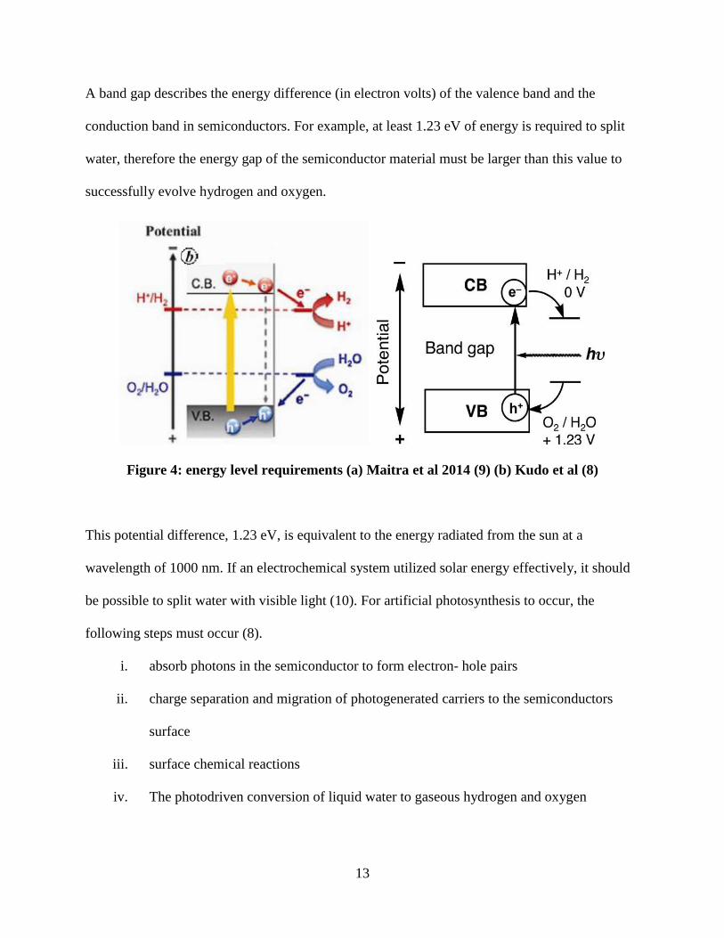
A band gap describes the energy difference (in electron volts) of the valence band and the
conduction band in semiconductors. For example, at least 1.23 eV of energy is required to split
water, therefore the energy gap of the semiconductor material must be larger than this value to
successfully evolve hydrogen and oxygen.
Figure 4: energy level requirements (a) Maitra et al 2014 (9) (b) Kudo et al (8)
This potential difference, 1.23 eV, is equivalent to the energy radiated from the sun at a
wavelength of 1000 nm. If an electrochemical system utilized solar energy effectively, it should
be possible to split water with visible light (10). For artificial photosynthesis to occur, the
following steps must occur (8).
i. absorb photons in the semiconductor to form electron- hole pairs
ii. charge separation and migration of photogenerated carriers to the semiconductors
surface
iii. surface chemical reactions
iv. The photodriven conversion of liquid water to gaseous hydrogen and oxygen
14
The semiconductor material must absorb the sunlight transmitted through the water (5). Once the
light is absorbed, electron-hole pairs will be formed. Charges (electrons and holes) must migrate
from their position in the thin film to the surface of the film. Materials with ideal crystal
structures allow for easy charge migration (6). This will increase carrier lifetime, i.e. the length
of time charges can move without recombining. Once charges reach the surface of their
respective electrodes, surface chemical reactions will occur (11). Electrons and holes at active
sites on the surface of the semiconductor will recombine with each other if reduction and
oxidation (redox) reactions do not occur. Redox reactions occur when electrons are transferred
from one species to another. After redox reactions occur, gaseous hydrogen and oxygen will
form on the cathode and anode, respectively (12).
Materials for SCLJ
Materials suitable to successfully create a SCLJ system are still being researched. Some common
materials that have been identified as potential PEC photoanodes are Titanium Dioxide (TiO2),
Tungsten Oxide (WO3), Iron Oxide (Hematite) (Fe2O3), Bismuth Vanadate (BiVO4). Numerous
other oxide and non-oxide materials have also been considered (5) (6). Each material has its
advantages and disadvantages.
Titanium Dioxide (TiO2)
In 1972, Honda and Fujishima published research using Titanium Dioxide as a material to
decompose water. This novel work sparked interest in the photolysis of water. Due to a large
bandgap, 3.2 eV (8), Titanium Dioxide is only active in the UV region of the solar spectrum. A
small external voltage bias must be applied to the anodes. TiO2 is very stable in all ranges of pH

15
solution (7), making the thin films versatile. Due to its versatility in solutions, it is typically used
to purify water, because it oxidizes organic material (8).
Tungsten Oxide (WO3)
Tungsten Oxide has a smaller band gap than TiO2, 2.8 eV (9), and is active in slightly longer
wavelengths of the solar spectrum. It is, however, not stable in acidic solutions (7). While the
material is limited in its spectral response, and solution stability, research is still being completed
to improve the performance through the use of colored dyes and material additives.
Iron Oxide (Hematite) (Fe2O3)
Hematite has a smaller bandgap, at 2.2 eV (9), and is active in the visible light range. Hematite is
not stable in acidic solutions (7), and lacks the ability to provide a long carrier lifetime. Carrier
lifetime refers to how long the charges (holes and electrons) stay active, until they reach the
surface of the material to react with the solution. This poor carrier lifetime limits the efficiency
of this material. Recent works have suggested that carrier lifetime can be improved with
selective coatings, dye sensitization, and nanostructuring (12).
Bismuth Vanadate (BiVO4)
Bismuth vanadate has recently emerged as a promising material for use as a photoanode (13).
Bismuth vanadate with a monoclinic scheelite structure has a high activity as a visible light
driven photocatalyst (14). The bandgap for bismuth vanadate is 2.4 eV (13), and it has been
shown to have good charge carrier properties and has exhibited stability in a wide variety of
conditions.

16
Fabrication Methods
At JMU, Thin films of Bismuth Vanadate have been deposited using Ultrasonic Spray Pyrolysis
(USP). This method is convenient, fast and economical technique to prepare films (14). The
ultrasonic spray pyrolysis method is one of multiple chemical solution based synthesis
techniques, including metal-organic decomposition, drop casting, spin coating, and dip-coating.
BiVO4 has also been fabricated using electrochemical deposition techniques and vacuum
deposition methods (13).
Conclusion
There are many methods to improve the photoelectrochemical properties of thin films. It has
been shown that high temperature annealing improves PEC performance in BiVO4 thin films
(13). Annealing thin films promotes formation of the monoclinic scheelite crystal structure (2).
Thin films can be annealed in air and also a 3% hydrogen atmosphere. A research group at James
Madison University studied the effects of tungsten doping on bismuth vanadate thin films. While
some groups saw an improvement of PEC performance in the thin films, Holland et al results
showed a decrease of performance. Performance variability was noted throughout the
photoanodes, in the doped and undoped samples. This led to the proposal that the performance
variability should be addressed before further research. It was identified that the source of the
variability might occur during the spray pyrolysis BiVO4 deposition process. Two likely sources
are slight variations in the nozzle height and the chemical composition of the precursor solutions.

17
Problem Statement
In this work, the effect of slight precursor composition variations in the film deposition process
on the PEC performance of BiVO4 photoanodes was investigated. This was done in an attempt to
isolate a potential source of PEC performance variability that may be attributed to the fabrication
process.

18
Procedures
To investigate the effects of precursor solution variability on thin-film BiVO4 photoanodes
produced via the ultrasonic spray pyrolysis method, a total of twelve different photoanodes were
fabricated. These twelve samples were produced according to the fabrication methods outlined in
the following sections. The PEC performance and material characteristics of these twelve
samples were evaluated according to the testing methods described in the following sections.
Bismuth Vanadate Photoanode Fabrication
As previously described, the thin-film photoanodes are produced by nebulizing a precursor
solution containing bismuth and vanadium compounds. To prepare the precursor solution for the
ultrasonic spray deposition process, stock solutions of bismuth nitrate and vanadium oxysulfate
were made. The bismuth source was a solution of 0.04 M Bismuth nitrate (Bi(NO3)3∙5H2O
(99.999%, Alfa Aesar)) in 0.5 M HNO3 (Fisher Scientific). A solution of 0.04 M vanadium
oxysulfate (VOSO4∙3.5H2O (99.9%, Sigma-Aldrich)) in 0.5 M HNO3 was prepared as the
vanadium source. The precursor solutions were then prepared from these stock solutions by
mixing the stock solutions in specific ratios to make the precursor solutions. Once deposited on
the heated substrates, the bismuth nitrate reacts with vanadium oxysulfate, to form bismuth
vanadate, and volatile byproducts that are carried away by exhaust gasses. Three precursor
solution ratios were mixed from stock solutions: 1 Bi: 1 V, 1.005 Bi: 0.995 V, 0.995 Bi: 1.005 V.
The 1 Bi: 1 V stock solution was mixed by combining 20 mL of the of bismuth nitrate and 20
mL vanadium oxysulfate; The 1.005 Bi: 0.995 V stock solution was mixed by combining 20.1
mL of the of bismuth nitrate and 19.9 mL vanadium oxysulfate; The 0.995 Bi: 1.005 V stock
solution was mixed by combining 19.9 mL of the of bismuth nitrate and 20.1 mL vanadium
19
oxysulfate. Approximately 10 mL of the precursor solutions were used for each thin-film
deposition, or fabrication, process. Before every deposition run, the precursor solution was
refilled to ensure trial consistency.
Test samples were produced for characterization using a variety of methods, including PEC
performance, film thickness measurements, film morphology characterizations. For tests that did
not require measurement the photoelectrochemical properties of the samples (i.e. film thickness,
morphology), the thin-film was deposited on glass microscope slides. This was chosen as the
substrate for such tests due to the inexpensive nature of glass slides. For measuring the electrical
properties of the samples, glass substrates coated with a thin, nominally transparent layer of
fluorine doped tin oxide (FTO) were used. In particular, TEC 7, a manufacturer’s designation
for the FTO coated glass substrates, were used for consistency with studies in the literature. In
the past, JMU researchers have determined that FTO provides the best interface with the BiVO4
thin film, as opposed to tin doped indium oxide (ITO), an alternative transparent conducting
material reported in the literature.
In preparation for deposition, all glassware and deposition system components were cleaned.
Substrates on which the BiVO4 was to be deposited were cleaned to ensure that no residue (e.g.
dust or fingerprints) was left on them. To begin the cleaning process, substrates were placed in
an acetone bath. The acetone was agitated by an ultrasonic cleaner for approximately ten
minutes. The substrates were then mechanically scrubbed, using a q-tip, with a solution of Dawn
dish detergent and water. The cleaned substrates were then placed in another ultrasonic bath
20
containing deionized water for approximately ten minutes. Once the substrate cleaning process
was completed, they were stored in isopropyl alcohol (IPA).
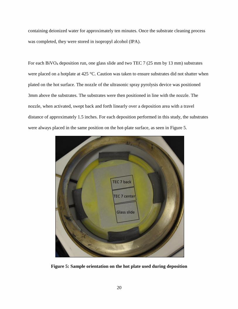
For each BiVO4 deposition run, one glass slide and two TEC 7 (25 mm by 13 mm) substrates
were placed on a hotplate at 425 °C. Caution was taken to ensure substrates did not shatter when
plated on the hot surface. The nozzle of the ultrasonic spray pyrolysis device was positioned
3mm above the substrates. The substrates were then positioned in line with the nozzle. The
nozzle, when activated, swept back and forth linearly over a deposition area with a travel
distance of approximately 1.5 inches. For each deposition performed in this study, the substrates
were always placed in the same position on the hot-plate surface, as seen in Figure 5.
Figure 5: Sample orientation on the hot plate used during deposition
Glass slide
TEC 7 center
TEC 7 back

21
Approximately 10 mL of the precursor solution was then placed over the ultrasonic transducer.
Small droplets of the precursor solution were formed via ultrasonic nebulization, which causes
small vapor droplets to form at the air-liquid interface due to the agitation provided by the
ultrasonic transducer. To date, at JMU, this droplet formation has been achieved by using
ultrasonic nebulizer operating at 1.7 MHz to agitate the liquid precursor. The droplets formed by
the nebulizer are then carried the substrate using dry, bottled air as a carrier gas at a flow rate of
6.9 L/min for 10 minutes. Figure 6 shows the setup for the ultrasonic spray pyrolysis apparatus.
The image on the left shows the ultrasonic transducer and the carrier gas while the image on the
right shows how the precursor solution mist is directed to the substrate through the translating
nozzle above the substrate on the hotplate surface.
Figure 6: Ultrasonic Spray Pyrolysis apparatus
Once the thin films were formed, they were removed from the hot plate carefully (as to not
damage the film formed or induce shattering of the glass substrates) and allowed to cool in
ambient room air. The produced thin films then received two annealing treatments – once in an
22
air environment and then in a reducing hydrogen atmosphere. It has been shown that annealing
BiVO4 thin films in air (at 500 ºC for 3 hours) promotes the formation of the desired photoactive
monoclinic scheelite phase (15). Annealing in a reducing environment (Air + 3 % hydrogen, 375
ºC, 3 hours) has been demonstrated to increase the number of oxygen vacancies in the material,
which is believed to result in increased electron transport through the material (15).
Once annealed, samples for photoelectrochemical testing were prepared by affixing a wire to the
exposed FTO substrate using a two-part silver epoxy (Epoxy Technology EE129-4). Samples
were then baked for 75 minutes at 97 ºC to cure the silver epoxy. Resistance measurements were
performed to ensure conductivity between the conducting substrate and the wire. Finally, the
wires and exposed conducting substrate were coated with clear insulating epoxy (2 Ton
insulating epoxy, Devcon) resulting in a BiVO4 photoanode samples with exposed surface areas
ranging from 0.84 to 1.5 cm2. Figure 7 illustrates the silver epoxy, clear epoxy, and exposed area
of a BiVO4 photoanode.

23
Figure 7:Illustration of the silver epoxy, clear epoxy, and exposed area of a BiVO4
photoanode that is immersed in Na2SO4 electrolyte solution for PEC testing
Photoelectrochemical Testing
Photoelectrochemical (PEC) testing is used to characterize the ability of the material to oxidize
water in the presence of sunlight. The reaction rate for oxygen production is directly proportional
to that for hydrogen production. That is, for every O2 molecule produced, two H2 molecules are
produced. One method of characterizing the PEC performance is to measure the rate and total
amount of oxygen (or hydrogen) produced. However, such a system to capture and monitor gas
evolution rates was not available for this investigation. An alternative method for testing the
photoelectrochemical performance of thin-films is to measure their electrical characteristics in a
three-electrode electrochemical cell. Because the water splitting process results in the transfer of
Silver Epoxy
Clear Epoxy
Exposed Area
24
ions, which in turn requires the transfer of electrons between the anode and cathode of the
electrochemical cell, the electrical current produced is directly proportional to the hydrogen and
oxygen evolution rate. Therefore, higher currents in the presence of sunlight indicate a greater
oxygen evolution rate and a higher light energy to hydrogen conversion efficiency.
Photoelectrochemical measurements were performed in a three electrode cell containing a 0.5 M
Na2SO4 (99.5%, Fisher Scientific) electrolyte with a phosphate buffer (pH 7.00±0.02 at 25 ºC,
Micro Essentials Laboratory). Because pure, deionized water is not electrically conductive, an
electrolyte solution is required for ion transport through the solution. However, the ions within
the electrolyte solution must not be oxidized or reduced at a potential lower than the redox
potential of water. The Na2SO4 solution meets this criterion, unlike NaCl, which will cause the
formation of Cl2, instead of O2 at the photoanode. Photoanodes of the produced BiVO4 films
served as the working electrodes for the electrochemical cell. A 4 M KCl Ag/AgCl electrode
(Accumet, Fisher Scientific) was used as a reference electrode and a platinum mesh served as the
counter electrode. All potential measurements reported herein are with respect to the Ag/AgCl
reference electrode.
A Keithley 2400 SourceMeter configured as a potentiostat was used to perform linear sweep
voltammetry at a sweep rate of 10 mV s-1. A potentiostat is a power supply that maintains a
desired set potential between the sample (or working electrode) and the reference electrode by
continuously adjusting the potential applied across the working electrode and the counter
electrode. For these tests, it was programmed to perform a linear sweep from -0.5 V to 1.5 V
across the working electrode with respect to the reference electrode. Voltammograms, or

25
measurements of current vs. applied potential, were obtained for all of the samples when
illuminated by simulated solar radiation with an intensity of 0.1 W cm2 at the sample surface.
The simulated solar illumination was produced with an Oriel 96000, 150 W solar simulator
(Newport) with an AM1.5 filter. The three electrode cell was placed 25.4 cm away from the solar
simulator to ensure the photoanode would receive approximately 0.1 W/cm2. A pyranometer was
used to confirm that the irradiance from the solar simulator was in fact 0.1 W/cm2, ensuring that
the testing setup mimicked natural sunlight.
Both front side illumination and through-substrate illumination conditions were investigated and
compared to dark current measurements. The front side of the sample is the side with the
exposed thin film. The back side of the sample is the TEC 7 substrate. Illumination from both
sides of the BiVO4 films were performed to study the electron transport through the BiVO4 film.
During each test, as the applied bias was varied from -0.5 V to 1.5 V, the light from the solar
simulator was intermittently blocked using an automated shutter system. The shutter closes and
opens at 0.05 V bias voltage intervals to obtain the dark current of the sample, for a total of 20 on
off cycles. The dark current obtained represents the current that is not produced due to the
incident light. To compare the photoelectrochemical performance of the different size BiVO4
photoanode samples, the measured current was normalized by the area exposed to the electrolyte
solution to obtain photocurrent density, J (mA/cm2).
All electrodes were rinsed in deionized (DI) water and dried with N2 gas prior to PEC testing.
The solar simulator was turned on and allowed to warm up. The three electrodes (BiVO4
photoanode, platinum mesh counter electrode, and reference electrode) were placed in
26
approximately 200 mL of the electrolyte solution. The photoanode was placed directly in the
middle of the beam from the solar simulator. The reference electrode was tested to ensure a flow
of KCl electrode solution through the frit. All electrodes were connected to the Keithley
Sourcemeter. A LabVIEW ™ interface that was programmed to control the Keithley
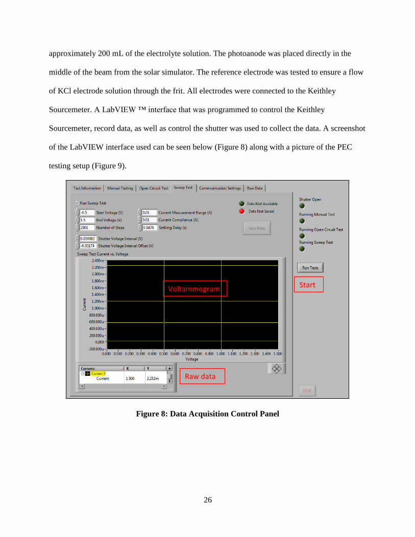
Sourcemeter, record data, as well as control the shutter was used to collect the data. A screenshot
of the LabVIEW interface used can be seen below (Figure 8) along with a picture of the PEC
testing setup (Figure 9).
Figure 8: Data Acquisition Control Panel
Voltammogram Start
Raw data

27
Figure 9: Photoelectrical chemical testing setup
Once data acquisition was completed for a sample, the resulting raw data files were saved. This
procedure was completed for every sample for the front and back side illumination conditions.
Once a PEC test was completed, each electrode was rinsed in DI water and dried in N2 gas. The
electrolyte solution was covered and the solar simulator was turned off.
Material Characterization
Thickness measurements were taken using a KLA Tencor P-7 surface profiler. Glass slides from
deposition runs were used to measure the thickness of the films by removing a tiny portion of the
thin-film to expose the glass substrate. This was done by making a small scratch down the edge
of the sample. This scratch allows the apparatus to measure the thickness of the film with respect
Connection for
Keithley
Solar Simulator
3 electrode cell
shutter

28
to the exposed glass slide. A small stylus is dragged across the surface of the thin film, as
illustrated schematically in Figure 10a, and the height of the stylus is recorded. The difference
between the height of the glass and the height of the rough BiVO4 material is used to determine
the film thickness. Thickness measurements are taken seven times (Figure 10b) per sample, to
ensure that a representative average thickness was obtained for each sample.
Figure 10: Surface thickness measurement (a) stylus and (b) locations on slides
Figure 11: Lauren Phillips performing thickness measurements
A LEO 1430VP scanning electron microscope (SEM) with an Oxford energy dispersive X-ray
spectrometer system (EDS) was used to analyze film morphology and chemical composition. For

29
examination with a SEM, small fragments were broken from a coated glass slide and a coated
TEC7 substrate and attached to a SEM mounting stub. The samples were coated with gold in a
low pressure argon environment. This was done to eliminate sample charging during SEM
imaging. The morphology of samples was investigated at 2000X-5000X magnification.

30
Results
Samples produced fall into one of three categories, based on the liquid precursor stoichiometric
ratios. Sample identification is presented in Table 1.
Table 1: PEC testing sample names
1 Bi: 1 V 1.005 Bi: 0.995 V 0.995 Bi: 1.005 V
BiVOx-115 BiVOx- 118 BiVOx- 121
BiVOx- 116 BiVOx- 119 BiVOx- 122
BiVOx- 117 BiVOx- 120 BiVOx- 123
Three deposition trials were performed for each Bi:V ratio tested. Each trial was given its own
identifier. Samples deposited on TEC7 from the same deposition trial were distinguished by their
location on the hot-plate (b- back, c-center) during the deposition process (see Fig. 5).
Sample Area
Areas of samples were approximated by measuring the length and width of the exposed (not
covered with 2-ton epoxy) BiVO4 surface and assuming the area to be rectangular. Figure 12
illustrates the definition of the exposed BiVO4 surface area.

31
Figure 12: Sample exposed area calculation for BiVO4-123b
𝐴𝑟𝑒𝑎 = 𝐿𝑒𝑛𝑔𝑡ℎ ∗ 𝑤𝑖𝑑𝑡ℎ = 0.8 𝑐𝑚 ∗ 1.5 𝑐𝑚 = 1.2 𝑐𝑚2
The exposed sample areas for all of the fabricated photoanodes are shown in Table 2. Exposed
sample areas ranged from approximately 0.84 cm2 to 1.5 cm2.
Table 2: Exposed sample area
Sample ID Sample Area (cm2) Sample ID Sample Area (cm2)
BiVOx-118c 0.84 BiVOx-123b 1.2
BiVOx-118b 1.12 BiVOx-115b 1.02
BiVOx-121c 0.98 BiVOx-115c 1.12
BiVOx-121b 1.26 BiVOx-117b 0.91
BiVOx-119c 1.26 BiVOx-120b 0.91
BiVOx-116b 1.12 BiVOx-122c 1.5
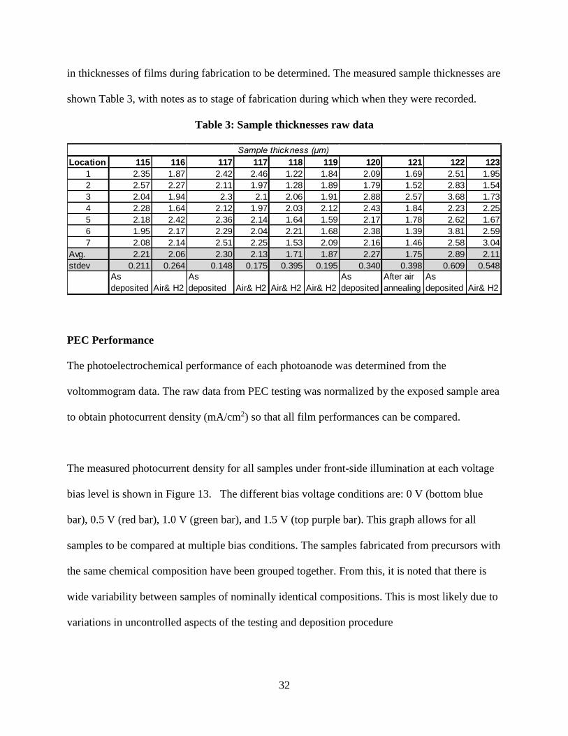
Sample Thickness
Sample thicknesses were determined using a KLA Tencor P-7 surface profiler. Thicknesses were
measured from the thin-films deposited on glass from various times in the fabrication processes
(post deposition, post air annealing, or post air and hydrogen annealing). This allowed for change
1.5 cm 0.8 cm
Epoxy
32
in thicknesses of films during fabrication to be determined. The measured sample thicknesses are
shown Table 3, with notes as to stage of fabrication during which when they were recorded.
Table 3: Sample thicknesses raw data
PEC Performance
The photoelectrochemical performance of each photoanode was determined from the
voltommogram data. The raw data from PEC testing was normalized by the exposed sample area
to obtain photocurrent density (mA/cm2) so that all film performances can be compared.
The measured photocurrent density for all samples under front-side illumination at each voltage
bias level is shown in Figure 13. The different bias voltage conditions are: 0 V (bottom blue
bar), 0.5 V (red bar), 1.0 V (green bar), and 1.5 V (top purple bar). This graph allows for all
samples to be compared at multiple bias conditions. The samples fabricated from precursors with
the same chemical composition have been grouped together. From this, it is noted that there is
wide variability between samples of nominally identical compositions. This is most likely due to
variations in uncontrolled aspects of the testing and deposition procedure
Location 115 116 117 117 118 119 120 121 122 123
1 2.35 1.87 2.42 2.46 1.22 1.84 2.09 1.69 2.51 1.95
2 2.57 2.27 2.11 1.97 1.28 1.89 1.79 1.52 2.83 1.54
3 2.04 1.94 2.3 2.1 2.06 1.91 2.88 2.57 3.68 1.73
4 2.28 1.64 2.12 1.97 2.03 2.12 2.43 1.84 2.23 2.25
5 2.18 2.42 2.36 2.14 1.64 1.59 2.17 1.78 2.62 1.67
6 1.95 2.17 2.29 2.04 2.21 1.68 2.38 1.39 3.81 2.59
7 2.08 2.14 2.51 2.25 1.53 2.09 2.16 1.46 2.58 3.04
Avg. 2.21 2.06 2.30 2.13 1.71 1.87 2.27 1.75 2.89 2.11
stdev 0.211 0.264 0.148 0.175 0.395 0.195 0.340 0.398 0.609 0.548
As
deposited Air& H2
As
deposited Air& H2 Air& H2 Air& H2
As
deposited
After air
annealing
As
deposited Air& H2
Sample thickness (μm)

33
Figure 13: Front side illumination current density
The backside illumination current density graph can be seen in Figure 14. The graph can be read
similarly, i.e., the bias conditions are 0 V (bottom blue bar), 0.5 V (red bar), 1.0 V (green bar),
and 1.5 V (top purple bar). The backside illumination current density is lower than for front side
illumination, as expected due to light absorption and reflection by the glass substrate, and
exhibits even greater variability.
1 Bi: 1 V 1.005 Bi: 0.995 V 0.995 Bi: 1.005 V

34
Figure 14: Backside illumination current density
Scanning Electron Microscopy
A scanning electron microscope (SEM) was used to characterize the morphology of the spray
deposited BiVO4 thin-films. It is typical for bismuth vanadate films to have a high surface
roughness & complex morphology (2), as illustrated in Figure 15, which presents an SEM
images obtained at 2000X-5000X magnification for sample BiVOx-117b. The small, partial
spherical structures are consistent with morphologies of USP deposited films investigated in
prior studies. It is believed that such a complex, highly porous morphology of the resulting films
significantly enhances the surface area available for the photooxidation processes and may help
to explain the state-of-the-art performance obtained from such samples.
1 Bi: 1 V 1.005 Bi: 0.995 V 0.995 Bi: 1.005 V

35
Figure 15: SEM image for BiVO4-117b
Energy dispersive X-ray spectroscopy (EDS) was used to determine the chemical composition of
the resulting BiVO4 films. EDS measurements confirmed that the atomic composition of the
deposited thin films were as expected. Table 4 shows the EDS results from the BiVOx-117b
sample.
Table 4: Energy Dispersive X-ray spectroscopy raw data for sample 117b (TEC 7)
Trial 1 Trial 2 Trial 3
Element Atomic % Element Atomic % Element Atomic %
O 57.09 O 58.41 O 55.92
V 14.66 V 14.85 V 14.24
Sn 12.14 Sn 12.13 Sn 13.52
Au 1.43 - - Au 1.92
Bi 14.67 Bi 14.61 Bi 14.4
36
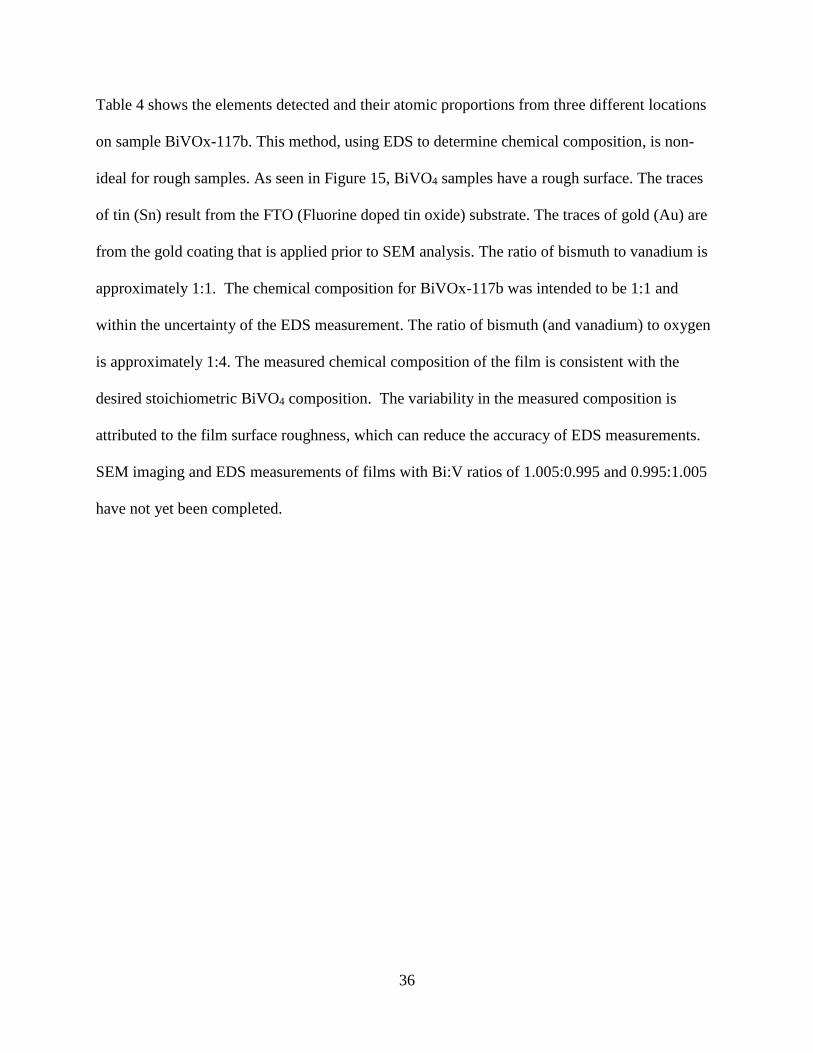
Table 4 shows the elements detected and their atomic proportions from three different locations
on sample BiVOx-117b. This method, using EDS to determine chemical composition, is non-
ideal for rough samples. As seen in Figure 15, BiVO4 samples have a rough surface. The traces
of tin (Sn) result from the FTO (Fluorine doped tin oxide) substrate. The traces of gold (Au) are
from the gold coating that is applied prior to SEM analysis. The ratio of bismuth to vanadium is
approximately 1:1. The chemical composition for BiVOx-117b was intended to be 1:1 and
within the uncertainty of the EDS measurement. The ratio of bismuth (and vanadium) to oxygen
is approximately 1:4. The measured chemical composition of the film is consistent with the
desired stoichiometric BiVO4 composition. The variability in the measured composition is
attributed to the film surface roughness, which can reduce the accuracy of EDS measurements.
SEM imaging and EDS measurements of films with Bi:V ratios of 1.005:0.995 and 0.995:1.005
have not yet been completed.

37
Analysis
After raw data was organized into meaningful charts and graphs, the results were analyzed.
Sample thickness results were organized based on chemical compositions.
Table 5: Sample Thicknesses data organized by chemical composition
Film Thicknesses 1:1 Ratio Bismuth rich Vanadium Rich
Average (μm) 2.18 1.95 2.25
Standard deviation 0.10 0.24 0.48
Variations can be seen in the film thicknesses. This is likely due uncontrolled factors in the
deposition process (e.g. the rate of atomization of the precursor by the ultrasonic transducer).
The PEC current density graphs shown in the results section (Figure 13- Figure 14) showed no
discernable trends with respect to chemical composition. Thus, it was concluded that small,
controlled variations had little effect on the PEC performance. To further investigate the results,
graphs were created based on film thickness and substrate location during deposition.
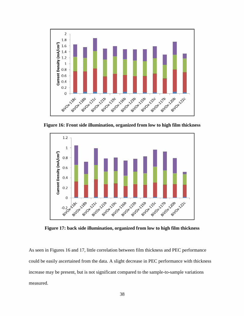
Figures 16 and 17 show PEC performance of films from low thickness (BiVOx-118c) to high
thickness (BiVOx-122c).
38
Figure 16: Front side illumination, organized from low to high film thickness
Figure 17: back side illumination, organized from low to high film thickness
As seen in Figures 16 and 17, little correlation between film thickness and PEC performance
could be easily ascertained from the data. A slight decrease in PEC performance with thickness
increase may be present, but is not significant compared to the sample-to-sample variations
measured.

39
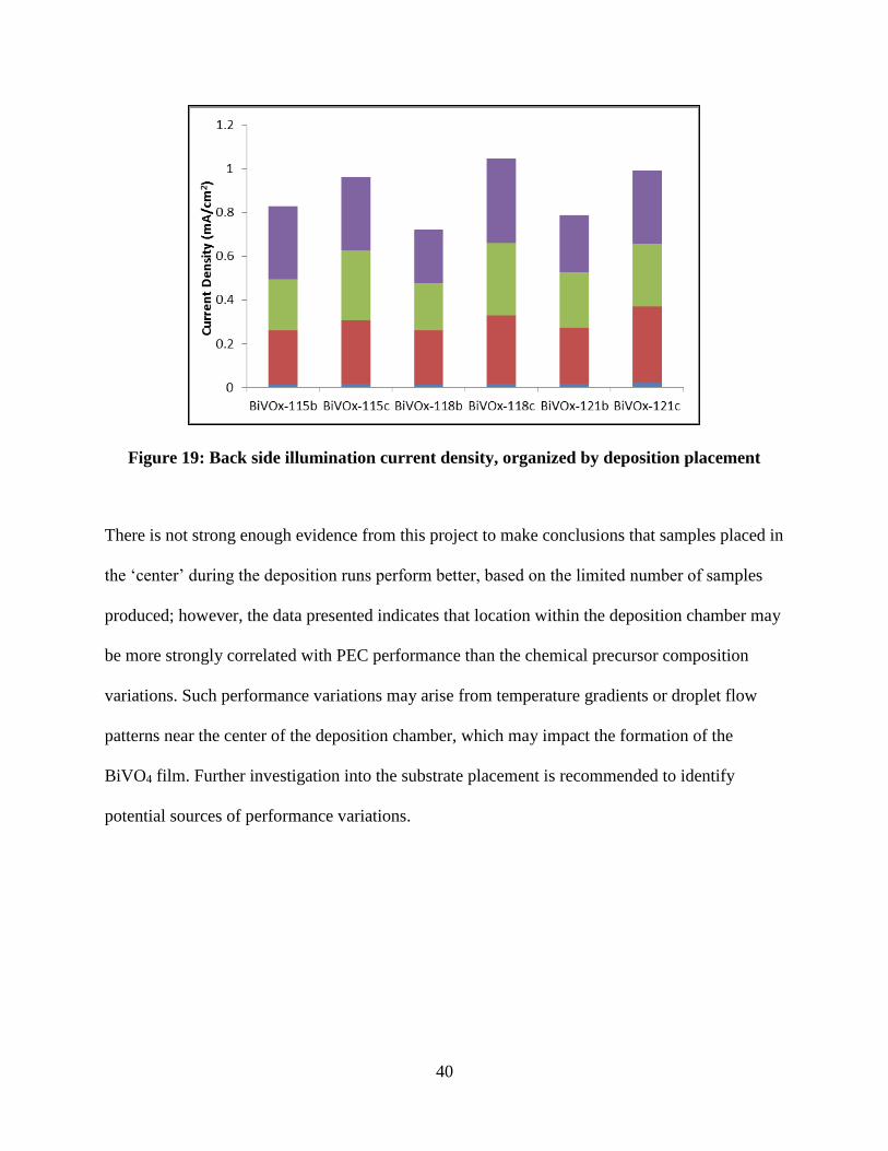
Samples that were created in the same deposition trial were also compared based on their
location in the deposition chamber during the deposition process, as described in Figure 5. It can
be seen in both front side illumination (Figure 18) and back side illumination (Figure 19) that the
TEC 7 substrate placed in the ‘center’ position exhibited slightly higher photocurrents relative to
those placed at the ‘front’ position.
Figure 18: Front side illumination current density, organized by deposition placement
40
Figure 19: Back side illumination current density, organized by deposition placement
There is not strong enough evidence from this project to make conclusions that samples placed in
the ‘center’ during the deposition runs perform better, based on the limited number of samples
produced; however, the data presented indicates that location within the deposition chamber may
be more strongly correlated with PEC performance than the chemical precursor composition
variations. Such performance variations may arise from temperature gradients or droplet flow
patterns near the center of the deposition chamber, which may impact the formation of the
BiVO4 film. Further investigation into the substrate placement is recommended to identify
potential sources of performance variations.

41
Conclusion
Twelve BiVO4 photoanodes were fabricated to investigate the effects of slight precursor
stoichiometry variations on the PEC performance. Precursor ratios of 1 Bi:1V, 1.005 Bi:1 V, and
1 Bi:1.005 V, were investigated. Based on the results presented herein, slight variations in the
Bi:V ratio in the precursor solutions exhibited little to no effect on the PEC performance.
Further investigation is suggested to determine the source of variability. Trends in data indicate
that the position of the substrate within the deposition chamber may be correlated with the
resulting PEC performance of the photoanodes. Specifically, substrates located at the center of
the deposition chamber exhibited slightly increased performance relative to those positioned at
the front of the chamber. Additional suggestions to improve the procedures and, to potentially
identify the sources of sample variability are to standardize the surface area measurement for
photocurrent normalization and to standardize the method in which photoanodes are placed in
the 3 electrode cell and aligned with the solar simulator for PEC testing.

42
Citations
1) Nocera, Daniel G. "The Artificial Leaf." Accounts Of Chemical Research 45.5 (2012):
767-776. Academic Search Complete. Web. 16 Mar. 2014.
2) Holland, S., Dutter, M., Lawrence, D., Reisner, B., and DeVore, C.,
“Photoelectrochemical performance of W-doped BiVO4 thin films deposited by spray
pyrolysis,” Proc. SPIE 8822, 8822- 14 (2013).
3) Armaroli, Nicola, and Vincenzo Balzani. "The future of energy supply: challenges and
opportunities." Angewandte Chemie International Edition 46.1‐2 (2007): 52-66.
4) Bard, A. J., and Fox, M. A., "Artificial photosynthesis: solar splitting of water to
hydrogen and oxygen," Acc. Chem. Res. 28, 141-145 (1995).
5) T. Bak, J. Nowotny, M.Rekas, C. Sorrell, “Photo-electrohemical hydrogen generation
from water using solar energy. Materials-related aspects,” International Journal of
Hydrogen Energy, 27 (2002) 991-1022.
6) F. Osterloh, “Inorganic nanostructures for photoelectrochemical and photocatalytic water
splitting,” Chem. Soc. Rev. (2012) DOI: 10.1039/c2cs35266d.
7) Currao, Antonio. "Photoelectrochemical Water Splitting." CHIMIA International Journal
for Chemistry 61.12 (2007): 815-19. Print
8) Kudo, Akihiko, and Yugo Miseki. "Heterogeneous photocatalyst materials for water
splitting." Chemical Society Reviews 38.1 (2009): 253-278.
9) Maitra, Urmimala, S. R. Lingampalli, and C. N. R. Rao. "Artificial Photosynthesis And
The Splitting Of Water To Generate Hydrogen. "Current Science (00113891) 106.4
(2014): 518-527. Academic Search Complete. Web. 16 Mar. 2014.
43
10) Fujishima, Akira. "Electrochemical photolysis of water at a semiconductor
electrode." nature 238 (1972): 37-38.
11) B. Alexander, P. Kulesza, I. Rutkowska, R. Solarska, J. Augustynski, “Metal oxide
photoanodes for solar hydrogen production,” J. Materials Chemistry (2008), 2298-2303.
12) K. Sivula, F. Le Formal, M. Gratzel, “Solar Water Splitting: Progress using Hematite (α-
Fe2O3) Photoelectrodes,” Chem. Sus. Chem. 4 (2011) 432-449.
13) Park, Yiseul, Kenneth J. McDonald, and Kyoung-Shin Choi. "Progress in Bismuth
Vanadate Photoanodes for use in Solar Water Oxidation." Chemical Society Reviews 42.6
(2013): 2321-37. ProQuest. Web. 16 Mar. 2014.
14) Li, Mingtao, Liang Zhao, and Liejin Guo. "Preparation And Photoelectrochemical Study
Of Bivo4 Thin Films Deposited By Ultrasonic Spray Pyrolysis." International Journal Of
Hydrogen Energy 35.13 (2010): 7127-7133. Academic Search Complete. Web. 16 Mar.
2014.
15) Wang, G., Ling, Y., Xihong, L., et al., “Computational and photoelectrochemical study of
hydrogenated bismuth vanadate,” J. Phys. Chem. C 117, 10957-10964 (2013).
Relevant Sources
Some relevant sources have been included for further investigation.
Abe, Ryu. "Recent Progress On Photocatalytic And Photoelectrochemical Water Splitting
Under Visible Light Irradiation." Journal Of Photochemistry & Photobiology C:
Photochemistry Reviews 11.4 (2010): 179-209. Academic Search Complete. Web. 16
Mar. 2014.

44
Bard, Allen J. "Light, Water, Hydrogen: The Solar Generation Of Hydrogen By Water
Photoelectrolysis." Journal Of The American Chemical Society 130.26 (2008): 8567-
8568. Academic Search Complete. Web. 16 Mar. 2014.
Chen, Xiaobo, et al. "Semiconductor-based photocatalytic hydrogen
generation." Chemical Reviews 110.11 (2010): 6503-6570.
Dunkle, S. S., Helmich, R. J., and Suslick, K. S., " BiVO4 as a Visible-Light
Photocatalyst Prepared by Ultrasonic Spray Pyrolysis," J. Phys. Chem. C 113, 11980-
11983 (2009).
Tributsch, Helmut. "Photovoltaic Hydrogen Generation." International Journal Of
Hydrogen Energy 33.21 (2008): 5911-5930.Academic Search Complete. Web. 16 Mar.
2014.