valve amplifier for proportional directional valves and
TRANSCRIPT

Bosch Rexroth AG, RE 30110-Z, edition: 2013-09
Contents
Configurations for VT-VSPA2-1-2X/V0/... 2Position of jumpers and adjustment elements 3Modification work 4Block diagram/pin assignment VT 3000, VT 3013, VT 3014, VT 3026 5Block diagram/pin assignment VT 3006, VT 3017, VT 3018 6Block diagram/pin assignment VT-VSPA2-1-1X/T1 7Block diagram/pin assignment VT-VSPA2-1-1X/T5 8Block diagram/pin assignment VT-VSPA2-50-1X/T1 9Block diagram/pin assignment VT-VSPA2-50-1X/T5 10Commissioning 11
Considering the prerequisites mentioned in this additional information, the analog amplifiers type VT-VSPA2-1-2X/V0/T1 and VT-VSPA2-1-2X/V0/T5 can be used as replacement for the following amplifier modules:
VT-VSPA2-1-2X/V0/T1 as replacement for: ▶ VT 3000-3X ▶ VT 3013-3X ▶ VT 3014-3X ▶ VT 3026-3X ▶ VT-VSPA2-1-1X/T1 ▶ VT-VSPA2-50-1X/T1
VT-VSPA2-1-2X/V0/T5 as replacement for: ▶ VT 3006-3X ▶ VT 3017-3X ▶ VT 3018-3X ▶ VT-VSPA2-1-1X/T5 ▶ VT-VSPA2-50-1X/T5
You must imperatively comply with the order of the work steps specified in this additional information!
Notices:Assembly of the product requires basic electrical knowledge:
▶ The product may only be re-wired and assembled by qualified personnel.
▶ De-energize the amplifier before any work!
H7125
Valve amplifier for proportional directional valves and proportional pressure valves, additional information
Information regarding the conversion of different amplifi-ers to amplifiers type VT-VSPA2-1-2X/V0/T1, material number R901002090 and amplifier type VT-VSPA2-1-2X/V0/T5, material number R901002095
RE 30110-Z Edition: 2013-09Replaces: 05.13Type VT-VSPA2-1-2X/V0/T1, .../T5
Inhalt
Contents 1Configurations for VT-VSPA2-1-2X/V0/... 2Position of jumpers and adjustment elements 3Modification work 4Block diagram/pin assignment VT 3000, VT 3013, VT 3014, VT 3026 5Block diagram/pin assignment VT 3006, VT 3017, VT 3018 6Block diagram/pin assignment VT-VSPA2-1-1X/T1 7Block diagram/pin assignment VT-VSPA2-1-1X/T5 8Block diagram/pin assignment VT-VSPA2-50-1X/T1 9Block diagram/pin assignment VT-VSPA2-50-1X/T5 10Commissioning 11Notes 12

2/12 VT-VSPA2-1-2X/V0/T1, .../T5 | Valve amplifier
Bosch Rexroth AG, RE 30110-Z, edition: 2013-09
Configurations for VT-VSPA2-1-2X/V0/...
Fact
ory
sett
ing
VT-V
SPA2
-1-2
X/V0
/...
VT
3026
1)
(RE
3009
3)O
bser
ve
foot
note
1)!
VT
3000
1)
(RE
2993
5)V
T 30
06 1
) (R
E 29
926)
Obs
erve
fo
otno
te 1
)!
VT
3013
(R
E 29
937)
VT
3017
(R
E 29
939)
VT
3014
(R
E 29
937)
VT
3018
(R
E 29
939)
VT-
VSPA
2-1-
1X/T
1 V
T-VS
PA2-
1-1X
/T5
(RE
3011
2)
VT-
VSPA
2-50
-1X
/T1
VT-
VSPA
2-50
-1X
/T5
(RE
3011
3)
Confi
gura
tion
for:
A4VG
…EP
2
.WRZ
(t
o co
mpo
nent
se
ries
6X)
D
BEP
6, 3
DRE
P6
(in
each
cas
e co
mpo
nent
se
ries
1X)
4WRA
64W
RA10
4WRA
6
(fro
m c
ompo
-ne
nt s
erie
s 2X
)
4WRA
10
(fro
m c
ompo
-ne
nt s
erie
s 2X
)
3DRE
P6
(fro
m c
ompo
nent
se
ries
2X)
, .W
RZ
(fro
m c
ompo
nent
se
ries
7X)
Inve
rsio
n
J1
Non
-inve
rtin
g Ju
mpe
r op
enJu
mpe
r op
enJu
mpe
r op
enJu
mpe
r op
enJu
mpe
r op
enJu
mpe
r op
enJu
mpe
r op
enJu
mpe
r op
en
Ram
p fu
nctio
n
J2Ra
mp
on
Jum
per
open
Jum
per
open
Jum
per
open
Jum
per
open
Jum
per
open
Jum
per
open
Jum
per
open
Jum
per
open
Ram
p tim
e
J330
ms
to 5
s
Jum
per
open
Jum
per
open
Jum
per
open
Jum
per
open
Jum
per
open
Jum
per
open
Jum
per
open
Jum
per
open
Step
func
tion
J4
Step
func
tion
on
Jum
per
open
Jum
per
open
Jum
per
open
Jum
per
open
Jum
per
open
Jum
per
open
Jum
per
open
Jum
per
open
Clo
ck fr
eque
ncy
J5, J
6 cl
osed
170
Hz
Sett
ing
by m
eans
of
pot
entio
met
er f
100
Hz ±
10%
2)
170
Hz
±10%
190
Hz
±10%
2)
Jum
per 6
ope
n 10
0 H
z ±1
0% 2
)30
0 Hz
±10
% 2)
180
Hz ±
10%
2)22
0 H
z ±1
0% 2
)
Max
imum
cur
rent
se
ttin
g
J7 c
lose
d15
00 m
ASe
ttin
g by
mea
ns
of G
w+
and
Gw
–60
0 m
A 2)
800
mA
2)15
00 m
A15
00 m
A25
00 m
A 2)
2500
mA
2)15
00 m
A
Step
leve
l J8
, J9
clos
ed50
0 m
ASe
ttin
g by
mea
ns
of S
+ an
d S–
200
mA
2)20
0 m
A 2)
500
mA
500
mA
350
mA
2)35
0 m
A 2)
500
mA
Tabl
e 1:
Con
figur
atio
ns V
T-VS
PA2-
1-2X
/V0/
T1 a
nd T
5
1)
Whe
n us
ing
the
ampl
ifier
s VT
-VSP
A2-1
-2X/
V0/.
.. as
rep
lace
men
t fo
r th
e am
plifi
er t
ypes
VT
3000
, VT
3006
and
VT
3026
, the
sup
ply
volta
ge m
ust
lie b
etw
een
28 a
nd 3
0 VD
C!
2)
Thes
e va
lues
mus
t be
set
!
In a
ll m
easu
rem
ents
, you
mus
t m
easu
re fr
om t
he m
easu
ring
soc
ket
"I"
agai
nst
"M0"
!Fo
r m
ore
info
rmat
ion
(cha
ract
eris
tic c
urve
s, e
tc. …
) re
fer
to t
he d
ata
shee
ts s
peci
fied
abov
e.
Plea
se n
ote:
Th
e or
der
of t
he fo
llow
ing
step
s m
ust
impe
rativ
ely
be o
bser
ved!

Valve amplifier | VT-VSPA2-1-2X/V0/T1, .../T5 3/12
RE 30110-Z, edition: 2013-09, Bosch Rexroth AG
�� ��� �����
��
��
�� ��
�����
��
���
�
������������������
������������
��
��
�
��
�
��
��
��
��
�������
Position of jumpers and adjustment elements
Measuring point selec-tor switch

4/12 VT-VSPA2-1-2X/V0/T1, .../T5 | Valve amplifier
Bosch Rexroth AG, RE 30110-Z, edition: 2013-09
Modification work
▶ VT-VSPA2-1-2X/V0/T1 serves as replacement for: – VT 3000, VT 3013, VT 3014, VT 3026,
VT-VSPA2-1-1X/T1, VT-VSPA2-50-1X/T1
▶ VT-VSPA2-1-2X/V0/T5 serves as replacement for: – VT 3006, VT 3017, VT 3018, VT-VSPA2-1-1X/T5,
VT-VSPA2-50-1X/T5
Re-wiring table
Terminal VT30... VT-VSPA2...1XVT-VSPA2-1-2X/V0/T1Terminal
VT-VSPA2-1-2X/V0/T5Terminal
2a Output switch-over ±9 V Not available 1) Not available 1)
2c – Ready for operation d22 d22
4a Call-up command value/ramp 2 d4 d4 and d12
4c Call-up switch-over ±9 V Not available 1) Not available 1)
6a Call-up command value/ramp 3 d6 d6 and d14
6c Call-up command value/ramp 4 d8 d8 and d16
8a Input command value 3 b6 b6
8c Call-up command value/ramp 1 d2 d2 and d10
10a Input command value 2 b4 b4
10c Input command value 1 b2 b2
12a Input command value 4 b8 b8
12c Input command value 5 Not available 1) Not available 1)
14a Ramp external d28 d28
14c Ramp external d24 d24
16a Differential input b14 b14
16c Differential input b16 b16
18a Command value output d30 d30
18c Call-up ramp off b12 b12
20a Measurement zero b28 b28
20c +9 V output b32 b32
22a Pin 1 solenoid B z6 z6
24a Pin 1 solenoid A z2 z2
26a 0 V input voltage z32 z32
26c Output –9 V b30 b30
28a Pin 2 solenoid B z8 z8
28c Call-up voltage relay z30 z30
30a Pin 2 solenoid A z4 z4
30c – Enable external d18 d18
32a +UB operating voltage z30 z30
32c +UB operating voltage – d18 d18
Table 2: Re-wiring
1) If the relevant function has previously been used, please refer to your sales contact partner.
The individual functions that are assigned to the relevant terminals are shown in the block diagrams on the follow-ing pages.
The following modification work must be made before the exact adjustment of the VT-VSPA2-1-2X/V0/T1 or T5:
▶ Card holder replacement: When replacing one of the amplifiers listed on the left by the amplifiers VT-VSPA2-1-2X/V0/T1 and T5, the existing card holder with the DIN female multipoint connector VT 3002-1-2X/32D must be additionally replaced by a card holder with the female multipoint connector VT 3002-1-2X/48F.
▶ Carry out the re-wiring according to the following table.
��
�
��
���
���
�����
���
����
����
����
����
����
����
�
��
�� ����
����
������
����
���
���
���
����
�
���
�������� �����
���
���
���
���
���
�� �
���
����
�
�
�����
���
� �
���
��
���
����
���
���
�
��
�
�
�
� ��
�
�
��
�
��
�
���
���
���
����� ��
�����
���
�
���
��
��
�
�
�
�
�
�
�
�
��
� �
�
��
� � � �
Valve amplifier | VT-VSPA2-1-2X/V0/T1, .../T5 5/12
RE 30110-Z, edition: 2013-09, Bosch Rexroth AG
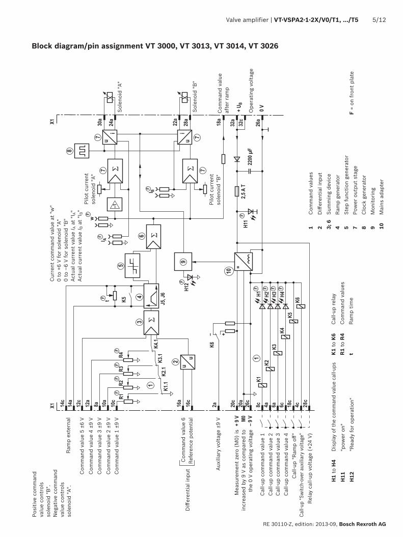
Block diagram/pin assignment VT 3000, VT 3013, VT 3014, VT 3026
H1
to H
4D
ispl
ay o
f the
com
man
d va
lue
call-
ups
H11
"pow
er o
n"
H12
"Rea
dy fo
r op
erat
ion"
Ram
p ex
tern
al
Posi
tive
com
man
d va
lue
cont
rols
so
leno
id "
B".
Neg
ativ
e co
mm
and
valu
e co
ntro
ls
sole
noid
"A"
.
1C
omm
and
valu
es
2D
iffer
entia
l inp
ut
3; 6
Sum
min
g de
vice
4Ra
mp
gene
rato
r
5St
ep fu
nctio
n ge
nera
tor
7Po
wer
out
put
stag
e
8C
lock
gen
erat
or
9M
onito
ring
10M
ains
ada
pter
K1
to K
6C
all-u
p re
lay
R1
to R
4C
omm
and
valu
es
tRa
mp
time
Com
man
d va
lue
5 ±6
V
Com
man
d va
lue
4 ±9
VC
omm
and
valu
e 3
±9 V
Com
man
d va
lue
2 ±9
VC
omm
and
valu
e 1
±9 V
Diff
eren
tial i
nput
Com
man
d va
lue
6 Re
fere
nce
pote
ntia
l
Auxi
liary
vol
tage
±9
V
Mea
sure
men
t ze
ro (
M0)
is
incr
ease
d by
9 V
as
com
pare
d to
th
e 0
V op
erat
ing
volta
ge
Cal
l-up
com
man
d va
lue
1C
all-u
p co
mm
and
valu
e 2
Cal
l-up
com
man
d va
lue
3C
all-u
p co
mm
and
valu
e 4
Cal
l-up
"Ram
p off
"Ca
ll-up
"Sw
itch-
over
aux
iliar
y vo
ltage
"Re
lay
call-
up v
olta
ge (
+24
V)
Cur
rent
com
man
d va
lue
at "
w"
0 to
+6
V fo
r so
leno
id "
A"
0 to
–6
V fo
r so
leno
id "
B"
Actu
al c
urre
nt v
alue
I A a
t "I
A"
Actu
al c
urre
nt v
alue
I B a
t "I
B"
Pilo
t cu
rren
t so
leno
id "
A"
Sole
noid
"A"
Sole
noid
"B
"
Ope
ratin
g vo
ltage
Pilo
t cu
rren
t so
leno
id "
B"
F =
on fr
ont
plat
e
Com
man
d va
lue
afte
r ra
mp

��
�
��
���
���
�����
���
����
����
����
����
����
����
�
��
�� ����
����
������
����
���
���
���
����
�
���
�������� �����
���
���
���
���
���
��
���
����
�
�
����
���
�
���
��
��
���
�
��
�
�
�
� ��
�
�
��
�
��
�
���
���
��� ��
���
���
�
���
��
��
�
�
�
�
�
�
�
��
� �
�
��
� � � �
����
����
����
����
���
���
���
���
���
6/12 VT-VSPA2-1-2X/V0/T1, .../T5 | Valve amplifier
Bosch Rexroth AG, RE 30110-Z, edition: 2013-09
Block diagram/pin assignment VT 3006, VT 3017, VT 3018
H1
to H
4D
ispl
ay o
f the
com
man
d va
lue
call-
ups
H11
"Pow
er o
n"
H12
"Rea
dy fo
r op
erat
ion"
Ram
p ex
tern
al
Posi
tive
com
man
d va
lue
cont
rols
so
leno
id "
B".
Neg
ativ
e co
mm
and
valu
e co
ntro
ls
sole
noid
"A"
.
1C
omm
and
valu
es
2D
iffer
entia
l inp
ut3;
6Su
mm
ing
devi
ce4
Ram
p ge
nera
tor
5St
ep fu
nctio
n ge
nera
tor
7Po
wer
out
put
stag
e8
Clo
ck g
ener
ator
9M
onito
ring
10M
ains
ada
pter
K1
to K
6C
all-u
p re
lay
R1
to R
4C
omm
and
valu
es
t1 to
t5
Ram
p tim
e
Com
man
d va
lue
5 ±6
VC
omm
and
valu
e 4
±9 V
Com
man
d va
lue
3 ±9
VC
omm
and
valu
e 2
±9 V
Com
man
d va
lue
1 ±9
V
Diff
eren
tial i
nput
Com
man
d va
lue
6 Re
fere
nce
pote
ntia
l
Auxi
liary
vol
tage
±9
V
Mea
sure
men
t ze
ro (
M0)
is in
crea
sed
by9
V as
com
pare
d to
the
0 V
ope
ratin
g vo
ltage
Cal
l-up
com
man
d va
lue
1C
all-u
p co
mm
and
valu
e 2
Cal
l-up
com
man
d va
lue
3C
all-u
p co
mm
and
valu
e 4
Cal
l-up
"Ram
p off
"C
all-u
p "S
witc
h-ov
er a
uxili
ary
volta
ge"
Rela
y ca
ll-up
vol
tage
(+2
4 V)
Cur
rent
com
man
d va
lue
at "
w"
0 to
+6
V fo
r so
leno
id "
A"
0 to
–6
V fo
r so
leno
id "
B"
Actu
al c
urre
nt v
alue
I A a
t "I
A"
Actu
al c
urre
nt v
alue
I B a
t "I
B" Pi
lot
curr
ent
sole
noid
"A"
Sole
noid
"A"
Sole
noid
"B
"
Com
man
d va
lue
afte
r ra
mp
Pilo
t cu
rren
t so
leno
id "
B"
F =
on fr
ont
plat
e
Ope
ratin
g vo
ltage

�� ��� �����
��
��
�� ��
�����
��
���
�
������������������
������������
��
��
�
��
�
��
��
��
��
�������
Valve amplifier | VT-VSPA2-1-2X/V0/T1, .../T5 7/12
RE 30110-Z, edition: 2013-09, Bosch Rexroth AG
Block diagram/pin assignment VT-VSPA2-1-1X/T1
H1
to H
4LE
D d
ispl
ay o
f the
com
man
d va
lue
call-
ups
K1
to K
6C
all-u
p re
lay
R1
to R
4C
omm
and
valu
es
Gw
aC
omm
and
valu
e at
tenu
ator
sol
enoi
d "A
"
Gw
bC
omm
and
valu
e at
tenu
ator
sol
enoi
d "B
"
Ram
p ex
tern
al
Posi
tive
com
man
d va
lue
(0 V
to 1
0 V
or
12 m
A to
20
mA)
co
ntro
ls s
olen
oid
"B".
1C
omm
and
valu
es
2D
iffer
entia
l inp
ut
3; 6
Sum
min
g de
vice
4Ra
mp
gene
rato
r
5St
ep fu
nctio
n ge
nera
tor
7PI
cur
rent
con
trol
ler
8O
utpu
t st
age
with
clo
ck g
ener
ator
9Po
wer
sup
ply
unit
10M
onito
ring
11C
able
bre
ak m
onito
ring
(o
nly
with
4 to
20
mA)
Com
man
d va
lue
5 ±6
VC
omm
and
valu
e 4
±9 V
Com
man
d va
lue
3 ±9
VC
omm
and
valu
e 2
±9 V
Com
man
d va
lue
1 ±9
V
Com
man
d va
lue
6 Re
fere
nce
pote
ntia
l
Auxi
liary
vol
tage
±9
V
Mea
sure
men
t ze
ro (
M0)
is in
crea
sed
by 9
V a
s co
mpa
red
to t
he 0
V o
pera
ting
volta
ge
Cal
l-up
com
man
d va
lue
1C
all-u
p co
mm
and
valu
e 2
Cal
l-up
com
man
d va
lue
3C
all-u
p co
mm
and
valu
e 4
Cal
l-up
"Ram
p off
"C
all-u
p "S
witc
h-ov
er a
uxili
ary
volta
ge"
Rela
y ca
ll-up
vol
tage
(+2
4 V)
Cur
rent
com
man
d va
lue
at "
w"
0 to
+6
V fo
r so
leno
id "
A"
0 to
–6
V fo
r so
leno
id "
B"
Actu
al c
urre
nt v
alue
I A a
t "I
A"
Actu
al c
urre
nt v
alue
I B a
t "I
B"
Sole
noid
"A"
Sole
noid
"B
"
"Rea
dy fo
r op
erat
ion"
Ope
ratin
g vo
ltage
F =
on fr
ont
plat
e
Nega
tive
com
man
d va
lue
(–
10 V
to 0
V
or
4 m
A to
12
mA)
co
ntro
ls s
olen
oid
"A".
Diff
eren
tial i
nput
Com
man
d va
lue
afte
r ra
mp
J7: E
nabl
e in
tern
al
Enab
le e
xter
nal (
+UB)
ZwZe
ro p
oint
com
man
d va
lue
Ba
Pilo
t cu
rren
t so
leno
id "
A"B
bPi
lot
curr
ent
sole
noid
"B
"t
Ram
p tim
e

�
����
���
�����
���
�
����
����
����
����
��
�
��
�� ����
��
��
������
����
���
���
���
�����
���
�������� �����
���
���
���
���
���
��� �
���
���
�
��
�
� �
��
�
���
����
���
���
���
��
���
���
����
���
����� ��
�����
����
���
���
�
�
����
�
�
�
� �
�
��
� �
�
�
�
��
� �
��
�
��
��
�
�� ��
�
�
��
��
�
� � � �
�
�
� ��
��
�
�
�
���
��
���
���
����
����
��
����
����
����
����
��
��
�
8/12 VT-VSPA2-1-2X/V0/T1, .../T5 | Valve amplifier
Bosch Rexroth AG, RE 30110-Z, edition: 2013-09
Ope
ratin
g vo
ltage
F =
on fr
ont
plat
e
Block diagram/pin assignment VT-VSPA2-1-1X/T5
H1
to H
4LE
D d
ispl
ay o
f the
com
man
d va
lue
call-
ups
K1
to K
6C
all-u
p re
lay
R1
to R
4C
omm
and
valu
es
Gw
aC
omm
and
valu
e at
tenu
ator
sol
enoi
d "A
"
Gw
bC
omm
and
valu
e at
tenu
ator
sol
enoi
d "B
"
Ram
p ex
tern
al
1C
omm
and
valu
es
2D
iffer
entia
l inp
ut
3; 6
Sum
min
g de
vice
4Ra
mp
gene
rato
r
5St
ep fu
nctio
n ge
nera
tor
7PI
cur
rent
con
trol
ler
8O
utpu
t st
age
with
clo
ck g
ener
ator
9Po
wer
sup
ply
unit
10M
onito
ring
11C
able
bre
ak m
onito
ring
(o
nly
with
4 to
20
mA)
Com
man
d va
lue
5 ±6
VC
omm
and
valu
e 4
±9 V
Com
man
d va
lue
3 ±9
VC
omm
and
valu
e 2
±9 V
Com
man
d va
lue
1 ±9
V
Com
man
d va
lue
6 Re
fere
nce
pote
ntia
l/G
ND
Auxi
liary
vol
tage
±9
V
Mea
sure
men
t ze
ro (
M0)
is in
crea
sed
by 9
V a
s co
mpa
red
to t
he 0
V o
pera
ting
volta
geC
all-u
p co
mm
and
valu
e 1
Cal
l-up
com
man
d va
lue
2C
all-u
p co
mm
and
valu
e 3
Cal
l-up
com
man
d va
lue
4C
all-u
p "R
amp
off"
Cal
l-up
"Sw
itch-
over
aux
iliar
y vo
ltage
"Re
lay
call-
up v
olta
ge (
+24
V)
Cur
rent
com
man
d va
lue
at "
w"
0 to
+6
V fo
r so
leno
id "
A"
0 to
–6
V fo
r so
leno
id "
B"
Actu
al c
urre
nt v
alue
I A a
t "I
A"
Actu
al c
urre
nt v
alue
I B a
t "I
B"
Sole
noid
"A"
Sole
noid
"B
"
"Rea
dy fo
r op
erat
ion"
Diff
eren
tial i
nput
Com
man
d va
lue
afte
r ra
mp
J7: E
nabl
e in
tern
al
Enab
le e
xter
nal (
+UB)
ZwZe
ro p
oint
com
man
d va
lue
Ba
Pilo
t cu
rren
t so
leno
id "
A"B
bPi
lot
curr
ent
sole
noid
"B
"t1
to t
5Ra
mp
times
Posi
tive
com
man
d va
lue
(0 V
to 1
0 V
or
12 m
A to
20
mA)
co
ntro
ls s
olen
oid
"B".
Nega
tive
com
man
d va
lue
(–
10 V
to 0
V
or
4 m
A to
12
mA)
con
-tr
ols
sole
noid
"A"
.

�
���
��
���
���
���
�����
���
����
����
����
����
�����
��
�
�
�� ����
��
��
������
���
� �
� �
���
�����
� �
� ����� �����
���
���
���
���
���
��� �
� �
��
���
��
��
��
�
���
�����
���
���
��
���
���
����
���
����� ��
�����
����
���
���
�
�
����
�
�
�
� �
��
� �
�
�
��
� �
�
��
�
��
��
��
� �
�
�
��
��
�
� � � �
�
�
� ��
��
�
�����
��
�
� �� �
�
Valve amplifier | VT-VSPA2-1-2X/V0/T1, .../T5 9/12
RE 30110-Z, edition: 2013-09, Bosch Rexroth AG
Block diagram/pin assignment VT-VSPA2-50-1X/T1
H1
to H
4LE
D d
ispl
ay o
f the
com
man
d va
lue
call-
ups
K1
to K
6C
all-u
p re
lay
R1
to R
4C
omm
and
valu
es
Ram
p ex
tern
al
1C
omm
and
valu
es
2D
iffer
entia
l inp
ut
3; 6
Sum
min
g de
vice
4Ra
mp
gene
rato
r
5St
ep fu
nctio
n
7PI
cur
rent
con
trol
ler
8O
utpu
t st
age
with
clo
ck g
ener
ator
9Po
wer
sup
ply
unit
10M
onito
ring
11C
able
bre
ak m
onito
ring
(o
nly
with
4 to
20
mA)
Com
man
d va
lue
5 ±6
VC
omm
and
valu
e 4
±9 V
Com
man
d va
lue
3 ±9
VC
omm
and
valu
e 2
±9 V
Com
man
d va
lue
1 ±9
V
Com
man
d va
lue
6 Re
fere
nce
pote
ntia
l/G
ND
Auxi
liary
vol
tage
±9
V
Mea
sure
men
t ze
ro (
M0)
is in
crea
sed
by 9
V a
s co
mpa
red
to t
he 0
V o
pera
ting
volta
ge!
Cal
l-up
com
man
d va
lue
1C
all-u
p co
mm
and
valu
e 2
Cal
l-up
com
man
d va
lue
3C
all-u
p co
mm
and
valu
e 4
Cal
l-up
"Ram
p off
"C
all-u
p "S
witc
h-ov
er a
uxili
ary
volta
ge"
Rela
y ca
ll-up
vol
tage
(+2
4 V)
Cur
rent
com
man
d va
lue
at "
w"
0 to
+6
V fo
r so
leno
id "
A"
0 to
–6
V fo
r so
leno
id "
B"
Actu
al c
urre
nt v
alue
I A a
t "I
A"
Actu
al c
urre
nt v
alue
I B a
t "I
B"
Sole
noid
"A"
Sole
noid
"B
"
"Rea
dy fo
r op
erat
ion"
Ope
ratin
g vo
ltage
Diff
eren
tial i
nput
Com
man
d va
lue
afte
r ra
mp
J7: E
nabl
e in
tern
al
Enab
le e
xter
nal (
+UB)
Zw (
R6)
Zero
poi
nt c
omm
and
valu
e
Ba
(R7)
Pilo
t cu
rren
t so
leno
id "
A"
Bb
(R8)
Pilo
t cu
rren
t so
leno
id "
B"
tRa
mp
time
F =
on fr
ont
plat
e
Posi
tive
com
man
d va
lue
(0 V
to 1
0 V
or
12 m
A to
20
mA)
co
ntro
ls s
olen
oid
"B".
Nega
tive
com
man
d va
lue
(–10
V to
0 V
or
4
mA
to 1
2 m
A)
cont
rols
sol
enoi
d "A
".

�
����
���
�����
���
�
����
����
����
����
�����
��
�
�
�� ����
��
��
������
���
� �
� �
���
�����
� �
� ����� �����
���
���
���
���
���
��� �
� �
��
���
��
��
��
�
���
�����
���
���
��
���
���
����
���
����� ��
�����
����
���
���
�
�
����
�
�
�
� �
��
� �
�
�
��
� �
�
��
�
��
��
��
� �
�
�
��
��
�
� � � �
�
�
� ��
��
�
�����
��
� �� �
���
���
����
����
��
����
����
����
����
��
��
�
10/12 VT-VSPA2-1-2X/V0/T1, .../T5 | Valve amplifier
Bosch Rexroth AG, RE 30110-Z, edition: 2013-09
Ope
ratin
g vo
ltage
H1
to H
4LE
D d
ispl
ay o
f the
com
man
d va
lue
call-
ups
K1
to K
6C
all-u
p re
lay
R1
to R
4C
omm
and
valu
es
Ram
p ex
tern
al
1C
omm
and
valu
es
2D
iffer
entia
l inp
ut
3; 6
Sum
min
g de
vice
4Ra
mp
gene
rato
r
5St
ep fu
nctio
n
7PI
cur
rent
con
trol
ler
8O
utpu
t st
age
with
clo
ck g
ener
ator
9Po
wer
sup
ply
unit
10M
onito
ring
11C
able
bre
ak m
onito
ring
(o
nly
with
4 to
20
mA)
Com
man
d va
lue
5 ±6
VC
omm
and
valu
e 4
±9 V
Com
man
d va
lue
3 ±9
VC
omm
and
valu
e 2
±9 V
Com
man
d va
lue
1 ±9
V
Com
man
d va
lue
6 Re
fere
nce
pote
ntia
l/G
ND
Auxi
liary
vol
tage
±9
V
Mea
sure
men
t ze
ro (
M0)
is in
crea
sed
by 9
V a
s co
mpa
red
to t
he 0
V o
pera
ting
volta
ge!
Cal
l-up
com
man
d va
lue
1C
all-u
p co
mm
and
valu
e 2
Cal
l-up
com
man
d va
lue
3C
all-u
p co
mm
and
valu
e 4
Cal
l-up
"Ram
p off
"C
all-u
p "S
witc
h-ov
er a
uxili
ary
volta
ge"
Rela
y ca
ll-up
vol
tage
(+2
4 V)
Cur
rent
com
man
d va
lue
at "
w"
0 to
+6
V fo
r so
leno
id "
A"
0 to
–6
V fo
r so
leno
id "
B"
Actu
al c
urre
nt v
alue
I A a
t "I
A"
Actu
al c
urre
nt v
alue
I B a
t "I
B"
Sole
noid
"A"
Sole
noid
"B
"
"Rea
dy fo
r op
erat
ion"
Diff
eren
tial i
nput
Com
man
d va
lue
afte
r ra
mp
J7: E
nabl
e in
tern
al
Enab
le e
xter
nal (
+UB)
Zw (
R6)
Zero
poi
nt c
omm
and
valu
e
Ba
(R7)
Pilo
t cu
rren
t so
leno
id "
A"
Bb
(R8)
Pilo
t cu
rren
t so
leno
id "
B"
t1 to
t5
Ram
p tim
es
Block diagram/pin assignment VT-VSPA2-50-1X/T5
F =
on fr
ont
plat
e
Posi
tive
com
man
d va
lue
(0
V to
10
V or
12
mA
to 2
0 m
A)
cont
rols
sol
enoi
d "B
".
Nega
tive
com
man
d va
lue
(–
10 V
to 0
V
or
4 m
A to
12
mA)
co
ntro
ls s
olen
oid
"A".

Valve amplifier | VT-VSPA2-1-2X/V0/T1, .../T5 11/12
RE 30110-Z, edition: 2013-09, Bosch Rexroth AG
Commissioning
Step 1 Set the relevant jumper according to table 1.
Step 2 Set the clock frequency. Use a digital multimeter suitable for frequency measure-ments in order to do so.Connect the digital multimeter with the measuring sockets "I" and "M0" and using the potentiometer f, set the frequency according to table 1.
Step 3: Set the step level.
Step 3.1: Apply +0.1 V at pin b14 at the differential amplifier input and connect pin b16 with 0 V.Using the S+ potentiometer, set the step level according to table 1.
Step 3.2: Apply –0.1 V at pin b14 and connect pin b16 with 0 V.Using the S– potentiometer, set the step level according to table 1.
Step 4: Set the maximum current.
Step 4.1: Apply +10 V at pin b14 and connect pin b16 with 0 V.Using the Gw+ potentiometer, set the maximum current according to table 1.
Step 4.1: Apply –10 V at pin b14 and connect pin b16 with 0 V.Using the Gw– potentiometer, set the maximum current according to table 1.
You must imperatively observe the additional information in the operating instructions RE 30110-B before commis-sioning the amplifier.

Bosch Rexroth AG, RE 30110-Z, edition: 2013-09
12/12 VT-VSPA2-1-2X/V0/T1, .../T5 | Valve amplifier
Bosch Rexroth AG HydraulicsZum Eisengießer 197816 Lohr am Main, Germany Phone +49 (0) 93 52 / 18-0 [email protected] www.boschrexroth.de
© This document, as well as the data, specifications and other information set forth in it, are the exclusive property of Bosch Rexroth AG. It may not be reproduced or given to third parties without its consent.The data specified above only serve to describe the product. No statements concerning a certain condition or suitability for a certain application can be derived from our information. The information given does not release the user from the obligation of own judgment and verification. It must be remembered that our products are subject to a natural process of wear and aging.
Notes