u.s. photovoltaic patents - national renewable energy · pdf file ·...
TRANSCRIPT

NRELlTP-210-4469 UC Category: 270 DE91015013 December 1991
u.s. Photovoltaic Patents: 1988-1990
Produced by the
Photovoltaics Division National Renewable Energy Laboratory 1617 Cole Boulevard Golden. CO 80401-3393
A Division of Midwest Research Institute
Operated for the
U.S. Department of Energy Under Contract No. DE-AC02-83CH10093

Contents
Introduction . . . . . . . . . . . . . . . . . . . . . . . . . . . . . . . . . . . . . . . . . . . . . . . . . . iii
Photovoltaic Patents 1988-1990 .................................. 1
Indexes
Assignee Index . . . . . . . . . . . . . . . . . . . . . . . . . . . . . . . . . . . . . . . 76 Inventor Index . . . . . . . . . . . . . . . . . . . . . . . . . . . . . . . . . . . . . . . . 84 Subject Index . . . . . . . . . . . . . . . . . . . . . . . . . . . . . . . . . . . . . . . . 106
I I
U.S. Patent Oec. 6, 19�J Sheel I or J 4.419.532
FIG. I
U.S. pa.ten�
F'IG.2 ,,, \ 12/!.
It!
ii Contents

Introduction
This document contains U.S. patents on terrestrial photovoltaic (PV) power applications, including systems, components, and materials, as well as manufacturing and support functions.
The patent entries in this document were Issued from 1988 through 1990. The entries were located by searching USPA, the data base of the U.S. Patent Office. The final search retrieved all patents under the class "Batteries, Thermoelectric and Photoelectric" and the subclasses "Photoelectric," "Testing," and IIApplications." The search also located patents that contained the words "photovoltaic(s)" or "solar cell(s)" and their derivatives. A manual search of the patents In the Solar Energy Research Institute (SERI) patent file augmented the data base search. After the initial list was compiled, most of the patents on the following subjects were excluded: space photovoltaic technology, use of the photovoltaic effect for detectors, and SUbjects only peripherally concerned with photovoltaics. Some patents on these three subjects were included when it appeared that those inventions might be of use in terrestrial PV power technologies.
How to Use This Document
The PV patent entries are arranged according to the patent number in ascending order, from the earliest to the most recent, and divided according to the year in which they were Issued. The entries for each patent include the inventor(s), the assignee, the title, the date of issue, and the abstract. Abstracts are reproduced in this document generally as they are found in the patents, except that statements referring to specific diagrams were modified or omitted because the document does not include illustrations.
The patents are indexed in this document by assignee, by inventor(s), and by subject. The three indexes follow the list of patent entries.
The subject index is divided according to 17 categories under three major divisions. Most patents are listed under two categories. The divisions and categories are as follows:
Cells and Materials
• Single-Crystal Silicon Cells • Polycrystalline and Ribbon Silicon Cells • Amorphous Silicon Cells • Cells from III-V Materials (e.g., GaAs) • Cells from 1-III-VI2 or II-VI Materials (e.g., CulnSe2 or
CdTe) • Other PV Devices and Concepts
• Cell Components (metalization, substrates, conductive coatings, anti reflective coatings)
• Cell Enhancement Techniques (surface and grainboundary paSSivation, annealing)
• Materials Production and Processes (purification, deposttion, doping)
• Characterization and Analysis
Collectors
• Flat-Plate Collectors (design, components, production)
• Concentrator Collectors (design, components, production)
• Optics and Trackers (lenses, reflectors, tracking devices, and related components)
Systems
• Utility-Interactive Systems and Interface Technologies (power conditioning)
• Utility-Independent Systems and Storage Technologies
• PV-Hybrid Systems (PV-thermal, photoelectrochemical)
• Systems Support (testing, maintenance, operation, and control)
How to Order a Copy of a U.S. Patent
Copies of patents can be obtained from the Patent and Trademark Office. A check or money order of $1.50 per patent, payable to the Commissioner of Patents and Trademarks, must accompany each order. The request must include the patent number(s); be sure to write clearly. Requests should be addressed to:
U.S. Department of Commerce Patent and Trademark Office Washington, D.C. 20231
Reference collections of U.S. patents are available to the public in Patent Depository Libraries (PDLs). Your local library should be able to refer you to the nearest PDL. The size and scope of these collections vary, and the hours that PDLs are open to the public vary as well. You may therefore want to contact the library for specific information about its collection and its hours to avoid inconvenience.
Introduction iii

Photovoltaic Patents 1988-1990

1988
4,717,790
Gochermann, Hans, inventor; Licentia PatentNerwaltungs GmbH, assignee. Contoured Solar Generator. January 5, 1 988.
A contoured solar generator whose solar cells and their associated electrical terminals and connecting lines are embedded in a laminate including at least the solar cells, an elastic thermosetting adhesive foil and a glass pane. To adapt the solar generator to a given external contour or to fit it into a given contour, the solar generator is configured as a curved laminate including at least one-dimensionally bent solar cells.
4,718,185
Conlin, Kevin L.; Cantrell, Michael P., inventors; Solar Signage, Inc., assignee. Modular Solar Generating System. January 12, 1 9S8.
A modular solar generating system is disclosed. The system includes a plurality of self-contained solar modules which are interconnectedly disposed in an array about the perimeter of a rigid framework housing a sign, light, or other load means necessitating electrical power during the night time hours. The modules themselves consist of a photovoltaic plate sandwiched between two suitable cover plates, including in this arrangement one or more continuous conductors. The modules are linked together by way of male and female plug connect�rs whereby the array may then be electrically connected to a battery. When the modular system is arranged in this fashion and exposed to incident sunlight for an appropriate period of time, power may be provided to a sign, light, or other electrical apparatus for nighttime use.
4,718,947
Arya, Rajeewa R., inventor, Solarex Corporation, assignee. Super/attice Doped Layers for Amorphous Silicon Phatavoltaic Cells. January 12, 1988.
Superlattice doped layers for amorphous silicon photovoltaic cells comprise a plurality of first and second lattices of amorphous silicon alternatingly formed on one another. Each of the first lattices has a first optical bandgap and each of the second lattices has a second optical band gap different from the first optical band gap. A method of fabricating the superlattice doped layers also is disclosed.
4,719,346
Taillebois, Jacques; Renaud, Jean-Marie; Perrot, Jean-Claude; Gambs, Paul, inventors; M.C.B., assignee. Optical Position Locating Apparatus with Bidirectional Ught Transmission. January 12, 1988.
2 U.S. Photovoltaic Patents: 1 988-1990
An optical position locating apparatus is provided which includes a first light reader with several photodetectors for reading the tracks of a disk, a first light emitter excited by the first light reader and a self-contained power supply source. A module is provided which comprises a second light emitter, a second light reader and a processor for processing electric signals from the first light reader. An optical fiber system is provided for transmitting the electric signals to the second light reader. Optical systems are advantageously provided.
4,721,535
Itoh, Haruo; Shimada, Toshikazu; Muramatsu, Shin-!chi; Matsubara, Sunao; Nakamura, Nobuo, inventors; Director-General of the Agency of Industrial Science and Technology, assignee. Safar Celf. January 26, 1988.
A solar cell including at least a thin film formed of an amorphous silicon material and having p-type conductivity. The thin film comprises a multi-layer structure including at least one non-doped layer formed of a material of an amorphous silicon matenal and having a thickness of 1 0 to 300 A and at least one p-Iype doped amorphous silicon layer of a given thickness. The p-type doped amorphous silicon layer is stacked such that at least one face thereof is in contact with said at least one non-doped layer of amorphous silicon material 50 that the thin film of multi-layer structure exhibits in effect p-type conductivity.
4,721,629
Sakai, Souich!; Nakano, Shoichi; Kuwano, Yukinori, inventors; Sanyo Electric Co., Ltd., assignee. Method of Manufacturing Phatovo/taic Device. January 26, 1988.
A transparent conductive film is formed on a glass substrate covering substantially its entire surface area and this transparent conductive film is divided into a plurality of transparent conductive parts per each photoelectric converting region. The photoelectric converting region is of a nearly rectangular shape, and accordingly, in order to divide the transparent conductive film into respective transparent conductive film parts, a laser beam is irradiated along all longitudinal and lateral sides of the rectangle. Thereby, the transparent conductive film parts corresponding to the photoelectric converting regions are formed as island regions. Semiconductor film parts are formed on the transparent conductive film parts divided into island regions corresponding to respective photoelectric converting regions and subsequently aluminum film parts are formed on these semiconductor film parts. Transparent conductive film parts are electrically connected to aluminum film parts of adjacent photoelectric converting regions. Thus, a photovoltaic device is manufactured wherein a plurality of photoelectric converting regions are formed on the substrate and respective photoelectric converting regions are connected in a series fashion.

4,721,986
Kinzer, Daniel M., inventor; International Rectifier Corporation, assignee. Bidirectional Output Semiconductor Field Effect Transistor and Method for Its Manufacture. January 26, 1 988.
A high voltage bidirectional output semiconductor field effect transistor (BOSFET) is disclosed which is turned on from the electrical output of a photDvoltaic stack which is energized from an LED. The process for manufacture of the device is also disclosed. The BOSFET device consists of two lateral field effect transistors formed in an implanted N(-) region in a P(-) substrate. Two spaced drain regions feed inwardly toward a common N( +) source region separated from the drains by respective P type diffusions. The surface of these diffusions can be inverted by application of voltage to the suitably disposed gate electrode. The depletion field between channel and drain regions is well controlled over the suriace of the device. The source contact remains close to the potential of the gate contact at all times so that the device can be used for high voltage switching of either polarity. A diode, PNP transistor and resistor are integrated into the same chip containing the lateral BOSFET device to form a solid state relay circuit having characteristics similar to a reed relay. The diode defines a forward conduction path from a photovoltaic pile voltage source directly to the BOSFET gate so that the BOSFET gate capacitance can be quickly charged during turn·on. The PNP transistor is a high gain transistor coupled to the diode and to the input resistance of the circuit. The input impedance of the circuit is reduced by the gain of the transistor when the photovoltaic output voltage is turned offand its voltage drops to below the gate voltage byabout 0.6 volt to turn an the transistor. This allows the BOSFET to quickly turn off as though the circuit had a relatively lowinput impedance. Another control circuit is disclosed which employs at dV/dt suppression clamp circuit and a regenerative turn-off circuit.
4,724,010
Okaniwa, Hiroshi; Nakatani, Kenji; Suzuki, Kazutomi, inventors; Teijin Limited, assignee_ SoJar Cell Module. February 9, 1988.
A solar cell module is made lightweight without a substantial lass of the periormance of the module by using a transparent hollow multilayer structure in which a plurality of transparent sheets are spaced at a distance by reinforcing members inserted between and connected to the transparent sheets as a window member as well as a supporting member of the module by disposing said transparent hollow multilayer structure on the light receiving side of a solar power generation element.
4,724,011
Turner. Gary B.; Morel, Don L.; Gay, Robert R.; Halani, Arvind; Tarrant, Dale E., inventors; AtlantiC Richfield Company, assignee. Solar Cell Interconnection by
Discrete Conductive Regions. February 9. 1988.
Cells of a thin film solar module having opposed upper and lower electrodes are connected in series by a plurality of discrete conductive regions extending between each upper electrode and the lower electrode of an adjoining cell. In a preferred embodiment, the opposite electrodes of adjoining cells overlap one another and one of the electrodes is a transparent conductive pad with a thickened metal·containing portion to aid in interconnection. In another embodiment, the conductive regions are formed by applying laser pulses to spaced locations along the areas of electrode overlap. after which a conductor may be deposited into cavities formed by the laser pulses.
4,725,558
Yamazaki, Shunpei; Suzuki, Kunia; Kinka. Mikio; Fukada, Takeshi; Abe, Masayoshi; Kobayashi, Ippei; Shibata. Katsuhiko; Susukida, Masato; Nagayama, Susumu; Koyanagi, Kaoru, inventors; Semiconductor Energy Laboratory Co., Ltd., assignee. Semiconductor Defects Curing Method and Apparatus. February 16, 1988.
An improved semiconductor defects curing method and apparatus are disclosed which is free from current leakage due to pin-holes or other defects. Also an improved method for processing a semiconductor device is shown. According to the invention, the gaps or holes in the semiconductor layer produced in the fabrication process are filled with insulator in advance of deposition of electrodes.
4,725,559
Fraas, Lewis M., inventor; Chevron Research Company, assignee. Process for the Fabrication of a Gallium Arsenide Grating Solar Cell. February 16, 1988.
A photovoltaic device is disclosed comprising a p-type conductive substrate. a sandwich of p-type AlyGa(l.y)AS bottom layer/p-Iype GaAs base layer/p'lype AlyGa(1.y�s top layer (wherein the suriace area of the p-type AlyGa(1.y)As top layer is less than the suriace area of the p-type GaAs base layer, a layer of n + -type GaAs emitter contacting the suriace of the p-type GaAs base layer (wherein the suriace area of the layer of n + -type GaAs emitter is less than one·tenth of the surface area of the p-type GaAs base layer). an insulating layer contacting the suriace of the p-type AlyGa(t .y)As top layer. and means for forming electrical contacts to the substrate and the incident surface of the n + ·type GaAs emitter layer.
4,725,740
Nakata, Yukihiko. inventor; Sharp Kabushiki Kaisha, assignee. DC·AC Converti.ng Arrangement for Photovoltaic System. February 16, 1 988.
Patents 3

An improved DC-AC converting arrangement for a photovoltaic system, which makes it possible to supply power at high efficiency by providing a driving control system arranged to stop operation of a DC-AC converter when a load power of the DC-AC converter falls below a predetermined reference value, and to restart the operation of the DC-AC converter when the load power exceeds the predetermined reference value.
4,726,044
Perna, Fred P.; Peterson, Stuart R., inventors; Fred P. Perna, assignee. Writing Instrument with Safar-Powered Electronic Counting and Uquid Crystal Display. February 16, 1 988.
A ballpoint pen of conventional size and shape has a movable ball point that is pressed upwardly in the direction of the housing of the pen when a mark is made. Means is provided for normally biasing the ballpoint outwardly of the housing. However, when the ballpoint is pressed against a writing surface, the refill cartridge having the ball at the lower end thereof is moved upwardly to close a normally open switch which connects a solar cell array in circuit with an electronic counter that counts each time the switch is closed. Controlled by the counter is a liquid crystal display that vi�ually indicates the total number of counts. A second switch is actuated by gravity to reset or clear the counter in preparation for counting a succeeding group of marks.
4,726,849
Murata, Kenji; Kishi, Yasuo, inventors; Sanyo Electric Co., Ltd., assignee. Photovoltaic Device and a Method of Manufacturing Thereof. February 23, 1 988.
A photovoltaic device comprises a glass substrate, and on a surface of the glass substrate, a plurality of transparent electrodes which define each photoelectric conversion cell are arranged at intervals. At one end of each transparent electrode in the direction of width thereof, a conductor and an insulator are formed so as to extend in parallel in the direction of length of the photoelectric conversion cell with a spacing maintained in between, for example, by means of screen printing. On the surface of the glass substrate, a semiconductor photoactive layer composed of amorphous silicon is formed so as to cover the transparent electrode and the conductor and the insulator stripes formed thereon. On the semiconductor photo-active layer, a back electrode composed of aluminum is formed. By irradiating a laser beam onto the insulator from the back electrode side, the irradiated part of the back electrode and the semiconductor photo-active !ayer thereunder are separated at each photoelectric conversion cell. Also, by irradiating the laser beam onto the conductor from the back electrode side, the irradiated part of the back electrode and the semiconductor photo-active layer thereunder are melted, and the back electrode of each photoelectric conversion cell is connected electrically to the adjacent transparent electrode through the
4 U.S. Pho1Dvoltaic Patents: 1988-1 990
conductor.
4,726,850
Wenham, Stuart R.; Green, Martin A., inventors; Unisearch Limited, assignee. Buried Contact Solar Cell. February 23, 1 988.
An electrical contact formed in a groove in the surface of a semiconductor material facilitates an advantageous contact with the material for a given cross-sectional area of contact when compared with a contact of the,same cross-sectional area formed on the surface of the material. The grooved contact significantly reduces shading of the surface of the semiconductor material compared with an equivalent surface contact.
4,726,851
Matsumura, Mitsuo; Yoshida, Toshihiko, inventors; Toa Nenryo Kogyo K.K., assignee. Amorphous Silicon Semiconductor Film and Production Process Thereof. February 23, 1 988.
This invention discloses an amorphous silicon semiconductor film comprising at least hydrogen, nitrogen, and oxygen as impurities and the method of producing it. The film is characterized in that the total quantity of nitrogen and oxygen in said film is at least 1 atom %. Since the film has a small light absorption coefficient and its optical refractive index is controllable, an excellent window material for solar cell can be provided. As adherence of the film with a metal electrode as well as with a transparent electrode is sufficient, good reproducibility in making solar cells using the film of this invention as window material was realized.
4,728,370
Ishii, Masayuki; Fujita, Nobuhiko; Hitotsuyanagi, Hajime, inventors; Sumitomo Electric Industries, Inc., assignee. Amorphous Photovoltaic Elements. March 1 , 1 988.
Disclosed are pin or nip type amorphous photovoltaic elements having the i-type layer comprised of an a-SiGe:H film, which are characterized in that an i-type amorphous silicon buffer layer is disposed between the layers of p-type and i-type and thus, the mutual diffusion of impurities andlor elements added to the i-type and/or the p-type layers through the p/i boundary is effectively restricted due to the presence of the buffer layer. As a result the formation of defects at the pli boundary and the deterioration of the p-type layer are effectively prevented, and the properties important to these kinds of devices, such as V oC' Jsc' FF being substantially improved, thereby making it possible to provide photovoltaic elements such as solar batteries having a practically acceptable long life span and a high reliability.

4,729,962 Campbell, Robert B., inventor; The United States of America as represented by the United States Department of Energy, assignee. Semiconductor Junction Formation by Directed Heat. March 8, , 988.
The process of the invention includes applying precursors with N- and P-type dopants therein to a silicon web, with the web then being baked in an oven to drive off excessive solvents, and the web is then heated using a pulsed high intensity light in a mechanism at 11000 to 1 1 500C for about 1 0 seconds to simultaneously form semiconductor junctions in both faces of the web.
4,730, 1 1 5 Abe, Koza, inventor; Logical Co., Ltd., assignee. Transformer System and Direct Current Power Supply. March 8, 1 988.
The present invention relates to a transformer system and a direct current power supply for obtaining a dc current Including a luminous body disposed on the primary side for converting electric power into a light and a solar cell unit disposed on the secondary side, opposing the luminous body, for receiving light emitted from the luminous body and for converting the light into electric power, thereby constituting a transformer which is further provided with an input control circuit and an output control circuit so as to configure a de power supply. According to this apparatus, a stable dc current can be obtained without generating the magnetic field and noise problems of typical wound core transformers.
4,730,602 Posnansky, Mario; Posnansky, Hernan, inventors. Apparatus for Automatically Directing Solar Radiation Focused by a Reflector. March 15, 1988.
For the tracking control of a reflector focusing the solar radiation on an absorber corresponding to the apparent movement of the sun, an adjusting mechanism of the reflector is driven by means of a direct-current motor. The terminals of the electric motor are connected to a parallel connection consisting of two solar cells. The parallel connection of both solar cells is such that they generate by constant radiation about a similar amount of voltage however with opposite polarity. The driving of the direct current motor takes place with the voltage differential occurring on the parallel connection. Both the solar cells are rigidly mounted to that part of the stationary arranged absorber on which part the solar rays are focused by the reflector. Both the solar cells are arranged symmetrical to the longitudinal axis of the absorber. With the help of the above described apparatus the reflector is automatically always so adjusted that the solar rays are focused on the absorber whereby no additional source of energy is necessary to drive the adjusting mechanism of the reflector.
4,732,621 Murata, Kenji, inventor; Sanyo Electric Co., Ltd., assignee. Method for Producing a Transparent Conductive Oxide Layer and a Photovo/taic Device Including Such a Layer. March 22, 1 988.
A method for processing a transparent conductive oxide (TCO) layer in accordance with the present invention comprises the steps of uniformly depositing the TCO layer on a substantially flat surface of a transparent substrate; and etching the exposed surface of the TCO layer thereof to roughen the exposed surface. The so-treated TCO layer is used as a transparent electrode in photovoltaic devices and has a decreased, substantially constant reflectance throughout the visible light range.
4,734,381 Mitchell, Kim W., inventor; Atlantic Richfield Company, assignee. Method of Making a Thin Film Cadmium Telluride Solar Cell. March 29, 1988.
A phosphorous doped layer of cadmium telluride is deposited onto a conductive window layer to form a thin film cadmium telluride solar cell. Back contacts to the solar cell are made by first depositing a layer of p conductivity type lead telluride upon the cadmium telluride and then depositing the metallic back contacts onto the lead telluride.
4,735,662 Szabo, Louis F.; Biter, William J., inventors; The Standard Oil Company, assignee. Stable Ohmic Contacts to Thin Films of p-type Tellurium-Containing II-VI Semiconductors. AprilS, 1988.
A stable ohmic contact for thin films of p-typs tellurium-containing IJ-VI semiconductors and photovoltaic devices incorporating such contacts. An ohmic contact according to the invention includes a contact-forming layer deposited on a p-type thin film of a tellurium-contacting II-VI semiconductor. Preferably, the contact-forming layer is copper having a thickness of about 2 nanometers. An isolation layer is deposited on the contact-forming to isolate subsequently deposited layers from the thin film. The iSOlation layer may be carbon or a thin layer of nickel. A connection layer for attaching an external electrical conductor is deposited on the isolation layer. The connection layer may be aluminum, chromium or a layer of copper, provided a copper Jayer is covered with one of silver, aluminum or a thin layer of nickel, preferably covered with aluminum. The stable, ohmic contact may be used as a back contact in a photovoltaic device incorporating a thin film of a tellurium-containing II-VI semiconductor as one of the active semiconductor layers in the device.
Patents 5

4,737,196 Yukimoto, Yoshinori, inventor; Mitsubishi Denki Kabushiki Kaisha, assignee. Amorphous Solar Cell. April 12, 1988.
An amorphous solar cell having a p·i�n (or n+p) structure, in which either or both of the p and n layers are of a double layer structure, including an amorphous semiconductor layer and a micro-crystalline semiconductor layer, wherein both layers are of the same conductivity type and the amorphous semiconductor layer is located at the side of the i layer.
4,737,197 Nagahara, Yoshiyuki; Shibata, Akira; Asai. Masahito; Nakajima, Shinichi; Takamori, Nobuyuki, inventors; Sharp Kabushiki Kaisha, assignee. Solar Cell with Metal Paste Contact. April 1 2, 1988.
A solar cell including a semiconductor substrate, a diffused layer provided in the semiconductor substrate by diffusion of dopant impurities, and an organic binder, a solvent, and an element belonging to the fifth group of the periodic table.
4,737,712 Stormont, Robert S.; Buchwald, Randall H.; Hashoian, Ralph S., inventors; General Electric Company, assignee. Isolated Power Transfer and Patient Monitoring System with Interference Rejection Useful with NMR Apparatus_ April 12, 1 988.
There is provided a power source for continuously energizing electrically isolated devices used to monitor the physiological state of a subject undergoing an examination in an NMR scanner having a magnet, RF and gradient coils. The power source is made up of a first element for generating energy of one type and a second element for receiving this energy and converting it to a second energy type used to energize the electrically isolated devices. The first and second elements are operatively coupled to one another through an electrically isolated medium to permit continuous transfer of energy from the first to the second element and to reject interference due to the NMR apparatus subsystems. In one embodiment the first element may be an array of light-emitting diodes, while the second element may be an array of photovoltaic cells. In another embodiment, the first and second elements may be ultrasonic transducers coupled through air or a ceramic substrate.
4,738,729 Yoshida, Toshihiko; Matsumura, Mitsuo; Yamamoto, Hideo; Asai, Kunia; Nakamura, Osamu; Okayasu, Yoshinobu, inventors. Amorphous Silicon Semiconductor Sofar Cell. April 1 9, 1988.
6 U.S. Photovoltaic Patents: 1988-1990
This invention discloses an amorphous silicon semiconductor film containing at least hydrogen, carbon and oxygen as impurities and the method to produce it. The firm is characterized in that the total quantity of carbon and oxygen in said film is at least 0,1 atom %.
Since the film has small light absorption coefficient and its optical refractive index is controllable, an excellent window material for solar cell can be provided. Since adherence of the film with a metal electrode as well as with a transparent electrode is sufficient. good reproducibility in making solar cells using the film of this invention as a window material was realized.
4,739,163 Gambs, Paul; Taillebois, Jacques; Renaud, Jean-Marie; Perrot, Jean-Claude, inventors; M.C.B., assignee. Position Locating Optical Coder Utilizing Optical Fiber. April 1 9, 1 988.
A position locating optical coder is provided formed by a sensor which includes a reader, for reading a code carrying element a pivoting micromirror actuated under the control of the output of the reader and a self contained power supply source. A module is provided which comprises two light emitters, a second reader, a unit for processing the Signals from the second reader, and a power supply source. In addition, a bidirectional coupler and optical fiber transmitting devices serve to transfer the code pulses between the sensor and the module.
4,739,383 Maruska, Paul H.; Hicks, Michael C.; Moustakas, Theodore D., inventors; Exxon Research and Engineering Company, assignee. Optical Detector and Amplifier Based on Tandem Semiconductor Devices. April 19, 1988.
If a semiconductor device is prepared so that it contains a photoconductive region in electrical series with a photovoltaic region, (i.e., a Schottky barrier or p-n junction) it can function as an optical amplifier and detector. When weak ac light plus an intense dc light are focused on this sample in an appropriate manner, the detected ac electric current will correspond to the intensity of the dc light but have the phase of the ac light; thus a weak ac light signal is effectively amplified, or a dc light signal is converted into an ae electrical signal capable of synchronous detection.
4,739,414 Pryor, Roger W.; Hudgens, Stephen J.; Nath, Prem; Mulberger, Ronald G., inventors; Ovanic Imaging Systems, Inc., assignee. Large Area Array of Thin Film Photosensitive Elements for Image Detection. April 1 9, 1 988.
Apparatus for producing electronic signals which are representative of a detectable condition on an image-bearing surface. The apparatus includes an elongated array of distinct thin film photosensitive elements formed on a common flexible large area

substrate. The elongated array of photosensitive elements are fabricated as a large area, photovoltaic structure formed of a plurality of thin film layers, including a first layer of thin film conductive material. The discrete photosensitive elements are defined by patterning of the conductive layer into shaped regions which determine the overall configuration and dimensions of each element.
4,740,431 Uttle, Roger G., inventor; Spire Corporation, assignee. Integrated Solar Cell and Battery. April 26, 1 988.
An Integrated solar cell and battery are described, together with a process of making the same. The integrated solar cell and battery are made by employing thin film deposition techniques on a substrate. Preferably first, a thin film solar cell is deposited on the substrate, as for example, by sputtering. This step is immediately followed by the deposition of a thin film battery, either onto the previously deposited thin film solar cell, or onto the back side of the substrate. The deposition process lends itself to automated production. The process includes the thin film deposition of series�connected arrays forming different types of integrated solar cells and batteries, depending on their electrical connections so as to vary the respective current and voltage characteristics of the resultant integrated units.
4,742,291 Bobier, Joseph A.; Brown, Gerald E., inventors; Bobier Electronics, Inc., assignee. Interface Control for Storage Battery Based Alternate Energy Systems. May 3, 1 988.
An alternate energy interface control for implementation with utility derived power sources and alternate power sources such as are provided by solar panels, windmills, and the like employed with systems utilizing storage batteries. The system monitors the current level of photovoltaic solar panels within intervals during such panels are connected with the battery storage source and further monitors the voltage levels developed by such panels during normal open circuit conditions thereof. A logic control is provided which monitors alternate source currents and voltage as well as storage battery voltage levels to prioritize the use of available alternate energy sources. Battery charging during periods of alternate power source availability is with a pulsed technique to enhance battery lifespans.
4,744,430 McCoy, Thomas R., inventor. Solar Powered Golf Cart. May 17, 1988.
A solar cell array is disclosed having a support structure, cover, and mechanically joined solar cell panels. Each panel, or group of panels, is electrically
connected across a separate battery and a diode is provided to provide separate charging of each battery and to prevent flow of current to the solar cells from the batteries.
4,744,835 Winstel, Guenter; Plaettner, Rolf, inventors; Siemens Aktiengesellschaft, assignee. Arrangement for Avoiding Unwanted Degradation in No-Load Operation of Solar Cell Modules Composed of Amorphous Silicon. May 17, 1988.
In order to avoid unwanted degradation in no-load operation Of solar cell modules composed, in particular, of amorphous silicon, an internal load resistor is integrated in the module and is connected across the output terminals during no-load operation of the module. Disconnection of the resistor during load operation occurs either in a mechanical manner by way of a mechanical switch integrated in a plug extending to the load or occurs automatically by way of an electronic switch. The arrangement is employed in operation of solar cell modules for systems having a non-continuous power consumption such as, for example, appliances in mobile homes, mountain chalets and the like.
4,745,078 Stetter, Walter; Peters, Winfried, inventors; Siemens Aktiengesellschaft, assignee. Method for Integrated Series Connection of Thin Film Solar Celfs. May 17, 1988.
The present invention relates to a method for providing integrated series connections of a plurality of solar cells each of which includes a photovoltaic thin film on a common transparent substrate which involves depositing a strip pattern of a material which is readily removable from the photovoltaic thin film onto the film at intervals dependent on the size of the solar cells, the strips of the pattern being offset laterally relative to the front electrodes lying under the thin film and extending over the regions of the thin film which are not to be covered by the subsequently back electrodes. Separating grooves are then mechanically generated in the film adjacent the strips. An electrically conductive metal is deposited over the entire suriace thus produced and finally the strip pattern is removed by lifting the pattern off the film, leaving gaps in the metallized layer forming the separated back electrodes of the solar cell.
4,746,370 Woolf, Lawrence D., inventor; GA Technologies, Inc., assignee. Photothermophotovoltaic Converter. May 24, 1 988.
A photothermophotovoltaic energy conversion system converts solar energy to electrical energy and includes a radiator and a photovoltaic cell. The photovoltaic cell receives incoming energy, including solar energy, and converts a first portion of the incoming energy to
Patents 7
electrical energy. The photovoltaic cell includes a reflector for reflecting a second portion of the incoming energy to the radiator to heat it. The heated radiator in turn radiates energy back to the photovoltaic cell for subsequent energy conversion therein of a first portion thereof. A second portion is reflected to the radiator, conserving heat.
4,746,371 McLeod, Paul S.; Cape, John A.; Fraas, Lewis M.; Partain, Larry D., inventors; Chevron Research Company, assignee. Mechanically Stacked Photovoftaic Cells, Package Assembly, and Modules. May 24, 1 988.
The present invention is an apparatus of mechanically stacked photovoltaic cells having a bottom heat spreader and a top heat spreader, a bottom photovoltaic cell and a top photovoltaic cell, and means for forming the necessary electrical contacts. The heat spreaders are electrically insulated from each other but are thermally connected to each other. The bottom photovoltaic cell has an anode and a cathode and is thermally bonded to the bottom heat spreader and is thermally connected to the top heat spreader. The top photovoltaic cell has an anode and a cathode, is electrically insulated from the bottom photovoltaic cell, and is thermally bonded to the top heat spreader and is thermally connected to the bottom heat spreader. The means for forming the necessary electrical contacts includes a means for electrically contacting the anode of the bottom photovoltaic cell. a means for electrically contacting the cathode of the bottom photovoltaic cell, a means for electrically contacting the anode of the top photovoltaic cell, and a means for electrically contacting the cathode of the top photovoltaic cell.
4,746,372 Tajika, Jun; Sano, Saijiro; Miyake, Tsuneo; Kuboi, Osamu, inventors; Kabushiki Kaisha Komatsu Seisakusho, assignee. Amorphous Silicon Solar Cel/s. May 24, 1 988.
An amorphous silicon solar cell comprising a glass substrate, a transparent conductive film formed on the glass substrate on one side thereof and having micro-columns or fine crystals irregularly formed on the other side, a plurality of amorphous silicon layers superposed on said other side of the conductive film, and a metal electrode formed on the superposed silicon layer. At the interiace between the transparent conductive film and the amorphous silicon layer is formed an intermediate layer in which both materials of the conductive film and the silicon layer are mixed. The intermediate layer has a refractive index between the conductive film and the silicon layer. The glass substrate may be substituted with a metal substrate, in which case the plurality of silicon layers are formed directly on the metal substrate, on which the transparent conductive film having an irregular suriace on the side opposite to the side where the silicon layers are formed and a metal electrode are
8 U.S. Pho1ovoltaic Patents: 1 988-1990
formed in this order.
4,746,458 Brotz, Gregory R., inventor. Photovo/taic Material. May 24, 1 988.
A photovoltaic material comprises an open-cellular foam material having an internal surface area with a photoelectric semiconductor material formed thereon. The material may further include a phosphor layer on the photoelectric layer.
4,746,618 Nath, Prem; Barnard, Timothy, inventors; Energy Conversion Devices, Inc., assignee. Method of Continuously Forming an Array of Photovoltaic Celfs Electrically Connected in Series. May 24, 1 988.
A method of continuously electrically interconnecting in series a plurality of smaller area photovoltaic cells from a continuous, elongated web of photovoltaic cell material which is maintained in continual motion.
4,748,130 Wenham, Stuart R.; Green, Martin A., inventors; Unisearch Limited, assignee. Method of Making Buried Contact Sotar Cell. May 31, 1 988.
An electrical contact formed in a groove in the suriace of a semiconductor material facilitates an advantageous contact with the material for a given cross-sectional area of contact when compared with a contact of the same cross-sectional area formed on the surface of the material. The grooved contact significantly reduces shading of the surface of the semiconductor material compared with an equivalent surface contact.
4,749,454 Arya, Rajeewa A.; Oswald, Robert S., inventors; Solarex Corporation, assignee. Method of Removing Electrical Shorts and Shunts from a Thin-Film Semiconductor Device. June 7, 1 988.
A method of removing electrical shorts and shunts from a thin-film semiconductor device having pairs of electrodes with exposed contact surfaces wherein each pair of electrodes is separated by a semiconductor film. The disclosed method comprises the steps of coating the exposed contact suriaces with an ionic solution and successively applying a reverse-bias voltage between the exposed contact suriaces of each pair of electrodes . The ionic solution has an etching rate that increases with increased temperature so that the leakage current flowing through shorts and shunts located between each respective pair of electrodes in response to the reverse-bias voltage will create a local temperature increase at the shorts and shunts and selectively etch or oxidize the shorts and shunts, rendering them substantially nonconductive. The exposed contact suriaces can be coated

using a sponge applicator or spray apparatus. The preferred ionic solution comprises an acid mixture diluted to one part in at least five parts water.
4,749,588
Fukuda, Nobuhiro; Ohashi, Yutaka; Miyaji, Kenji, inventors. Process for Producing Hydrogenated Amorphous Silicon Thin Film and a Solar CelJ. June 7, 1988.
The speed of forming a film of a hydrogenated amorphous silicon (a-Si:H) can be increased by controlling the amount of a supplied energy in relation to the film-forming speed. Application of this technique to the production of a solar cell enables a hydrogenated amorphous silicon solar cell (a-Si:H cell) having a high photoelectric conversion efficiency to be produced at high speeds. The aforesaid controlling procedure comprises adjusting the amount (KJ/g-Si2H6) of an energy to be supplied to a film-forming speed depends mainly upon the flow rate of the gas and is not substantially affected by the amount of the energy.
4,749,982
Rikuna, Kenji; Nakano, Harumi; Kara. Kazuya; Shigenaga, Yoshimi; Bito, Hiroyasu; Takeuchi, Elichi; Tamiya, Morita, inventors; Casio Computer Co., Ud., assignee. Intelligent Card. June 7,1988.
In an intelligent card, a keyboard has numeric keys for entering identification information and a collation execution key. A solar cell, a display device and an IC chip for performing arithmetic operations and card identification are incorporated in a case. The IC chip includes a nonvolatile memory for storing predetermined identification information. The predetermined identification information is compared with the input identification information entered at the keyboard upon operation of the key, thereby performing card identification.
4,750,099 Inoue, Yuichi; Ohtawa, Shuji; Ochiai, Hitoshi; Kiyono, Yoshihiko; Nakamura, Chiaki, inventors; Seiko Instruments, Inc., asSignee. Circuit for Charging Capacitors. June 7,1988.
A circuit for charging capacitors having a power source, a plurality of capacitors for accumulating an electric charge from the power source, switching elements with electrically controllable inputs for connecting or disconnecting at least one of the capacitors to or from the power source, and resistors for setting the switching elements to turn off. These resistors are connected to the control inputs of the switching elements and to one of two terminals of the power source directly so that the resistors consume the electric charge only when the power source supplies the electric charge.
4,751,191
Gonsiorawski, Ronald C.; Czernienko, George, inventors; Mobil Solar Energy Corporation, assignee. Method of Fabricating Solar Cells with Silicon Nitride Coating. June 14, 1988.
A process of manufacturing silicon solar cells with efficiencies of between about 12.5% and about 16.0% is described, the method being characterized by forming a PIN junction adjacent the front surface of a silicon substrate, subjecting the front surface of the substrate to a selected plasma surface etch treatment, and then forming a polysilazane coating on the etched front surface by (8) first subjecting the substrate to an ammonia plasma treatment for a predetermined period of time so as to produce hydrogen implantation and (b) subjecting the substrate to a silane and ammonia plasma treatment to obtain additional hydrogen implantation and formation of a polysilazane (hydrogenated silicon nitride) coating. The polysilazane coating is etched to form a grid electrode pattern. An aluminum coating is applied to the rear side of the substrate so as to form a back electrode. The aluminum coating is heated so as to alloy with the silicon substrate and thereby form an ohmic contact. The alloying step also densities the polysilazane so that it is more nearly silicon nitride. The exposed silicon on the front side of the substrate is coated with an adherent coating of a highly conductive metal so as to form a grid electrode.
4,751,413
Izawa, Hideo, inventor; Sharp Kabushiki Kaisha, assignee. Solar Energy Motor. June 14, 1988.
A solar energy motor comprises a plurality of photovoltaic elements, such as solar cells, and armature coils unistructurally secured to a rotatable axis. The photovoltaic elements and the armature coils are electrically connected such that DC electromotive forces generated sequentially in the photovoltaic elements on which light beams are made incident are applied to the armature coils. Currents thus generated in the armature coils produce a torque in the presence of magnets.
4,751,622
Williams, Lloyd E., inventor; Power Plus, Inc., assignee. SoJar Powered Construction Ught. June 14, 1988.
A solar powered construction light including a solar powered battery recharging network that recharges a storage battery at a constant rate and can be selectively operated to burn continuously to produce a continuous light or to burn intermittently to provide a flashing light. A solar cell recharges the storage battery in the light when sunlight is impinging upon the solar cell to provide virtually maintenance free and long term operation of the construction light during the dark or twilight hours when construction lights are commonly employed to warn motorists of road hazards.
Patents 9

4,753,683
Ellion, M. Edmund; Wolff, George, inventors; Hughes Aircraft Company, assignee. Gallium Arsenide Solar Cell System . June 28, 1988.
A solar cell array utilizing geometrically alternating, laterally disposed N-on-P and P-on-N gallium arsenide solar cells is disclosed. Improved array efficiency is achieved by placing adjacent solar cells in substantial contact with each other and eliminating bus connections on H'e top surfaces. This is accomplished by providing the solar cells with a lateral cross-sectional configuration of a parallelogram with the N-on-P solar cells slanted in one lateral direction and the P-on·N solar cells slanted in the opposite direction. The top surfaces of adjace�t, contacting solar cells are electrically connected by extending a connector grid across the top surfaces. Strip connectors are used to join the bases of adjacent solar cells.
4,753,684
Ondris, Miroslav; Pichler, Marty A., inventors; The Standard Oil Company, assignee. Photovoltaic Heterojunction Structures. June 28, 1988.
A three layer, photovoltaic structure having polycrystalline semiconductor layers dispos
-ed in series
optically and in sequential touching contact includes a relatively wide optical bandgap energy window layer, a light-absorbing layer and a third, relatively wide bandgap energy layer that forms a minority carrier mirror with the light-absorbing layer. All three layers have different compositions so that the structure includes two heterojunctions. The light-absorbing layer and third layer are of the same conductivity type. The structure is conveniently realized using II-VI semiconductor compounds such as cadmium sulfide or zinc sulfide window layer, a mercury cadmium telluride, cadmium telluride, zinc cadmium telluride or mercury zinc telluride light-absorbing layer and a third layer of cadmium telluride, zinc telluride, zinc cadmium telluride, mercury cadmium telluride or cadmium manganese telluride. Cadmium is present in at least two of the three layers of the novel structures. Tellurium is present in two of the three layers. Structures according to the invention may be conveniently for�ed by electrodeposition and may employ opaque or transparent substrates depending on the particular semiconductor materials used and their relative positions.
4,754,271
Edwards, Willie, inventor. Uquid Crystal Photograph. June 28, 1988.
A device for electronically generating a plurality of single still pictures which are stored in the device's self-contained programmed digital memory cartridge and which is displayed on a liquid crystal screen. The device is a structure resembling a thin pocket calculator.
10 U.S. Photovoltaic Patents: 1988-1990
4,754,418
Ham, Kazuya, inventor; Casio Computer Co., Ltd., assignee. Combined Electronic Calculator and Credit Card. June 28, 1988.
A key input unit, a display unit and a solar cell are arra�ged on one surface of a card-like electronic calculator. This surface serves as an electronic calculator. The outer shape of the card-like electronic calculator is the same as that of a credit card. Furthermore, a magnetic stripe portion on which predetermined data is recorded, and embossed portions for displaying information are formed on the other surface of the calaculator. Therefore, the calculator also serves as a credit card.
4,754,544
Hanak, Joseph J., inventor; Energy Conversion Devices, Inc., assignee. Extremely Ughtweight, Flexible Semiconductor Device Arrays. July 5, 1988.
An extremely lightweight, interconnected array of semiconductor devices, such as solar cells, is formed from a large continuous area of semiconductor material disposed on an unconventionally thin, electrically conducting substrate. The interconnections are formed by removing portions of the substrate to form substrate islands underlying a layer of semiconductor material which underlies a transparent conductive oxide. The oxide layer may likewise be formed into mutually isolated islands that overlay the areas between the substrate islands. Individual units or cells so formed may be interconnected by depositing a conducting material on, alongside and at least partially between islands of oxide and/or semiconductor, by depoSiting a metal grid on the oxide layer and burning conducting paths to the substrate islands, or by pierCing the layers and disposing a conducting material in the holes pierced.
The unconventionally thin substrate may be a sheet of electroformed nickel or other thin metal or an initially thick substrate that is thinned by chemical etching after other array processing steps are completed. An encapsulant is preferably applied to the exposed surface of the semiconducting material to protect it while the substrate is being thinned or removed. Subsequently, an encapsulant is applied to the rear of substrate side of the array.
4,755,231
Kurland, Richard M.; Allard, Ira L.; Chaky, Rebecca C.; Inouye, George T., inventors; TRW Inc., assignee. Flexible Solar Array Cell and Substrate Therefor. July 5, 1988.
A substrate structure for lightweight, flexible solar cell arrays, in which a plastic substrate is provided with a structure for discharging accumulations of electrons on its rear face and has appropriate heat emmissivity properties. In one embodiment, a Kapton

substrate layer is coated with a grounded aluminum layer, which is suitably painted for emissivity. In another embodiment, a poorly conductive Kapton substrate layer, impregnated with carbon, is used to dissipate the charge, and to provide the approppriate emissivity. In a third embodiment, a grounded VDA layer is sandwiched between two Kapton layers.
4,755,483
Haku, His,ao; Nakashima, Yukio; Matsuoka, Tsugufumi; Watanabe, Kaneo, inventors; Sanyo Electric Co., Ltd., assignee. Method for Producing Semiconductor Device with P-Type Amorphous Silicon Carbide Semiconductor Film Formed by Photo-Chemical Vapor Deposition. July 5,
1988.
A method for producing a semiconductor device uses 1rimethyl boron (B(CH,),) of triethyl boron (B(C2H5h) or a mixture thereof as a p-Iype dopant and/or a band gap widening source material gas in a process for forming a p-type amorphous semiconductor film. Accordingly, the quantity and the number of different gases which are used can be reduced and also the photoconductivity and dark conductivity can be improved, whereby a semiconductor device suitable for photovoltaic cells, photo sensors and the like using a p-type amorphous semiconductor film having a wide optical band gap can be produced.
4,755,804
Levati, Aldo; Siviero, Pietro, inventors; T elettra Telefonia Elettronica e Radio S.p.A., assignee. System for Feeding and Controlling Low Intensity Obstruction Ughts. July 5, 1 988.
A system for feeding and controlling low intensity obstruction lights, involving low power drain especially in radio stations powered by solar cells includes: (1) a SUb-system which not only generates the energy necessary to feed the obstruction light, but also detects solar intensity; (2) a control sub-system which delivers energy to the obstruction lights, triggered in correspondence to a light threshold, generates indicator signals on the operating state of the main onloff switch and the power circuit breaker and generates a lamp failure control for telemetering purposes and fault controls for the individual obstruction lights for local displaying purposesj and a low luminous intensity and low power drain lighting SUb-system.
The installation to actuate the system described includes: (1 ) an electrical energy distributor powered by solar cells and respective batteries via a regulator, a light sensor, a sub-rack equipped with a control module and a switch-over module for each light; (2) 2·filament lamps with lenticular light globe of the oriented Fresnel prisms type.
4,756,074
Lewis, Carol R., inventor; Varian Associates, Inc., assignee. Method of Making a High Conductance Ohmic Junction for Monolithic Semiconductor Devices. July 12, 1988.
In order to increase the efficiency of solar cells, a monolithic stacked device is constructed comprising a plurality of solar sub-cells adjusted for different bands of radiation. The interconnection between these sub-cells has been a Significant technical problem. The invention provides an interconnection which is a thin layer of high ohmic condUctance material formed between the sub-cells. Such a layer tends to form beads which serve as a shorting interconnect while passing a large fraction of the radiation to the lower sub-cells and permitting lattice-matching between the sub-cells to be preserved.
4,758,525
Kida, Yasuhiro; Suda, Koichi; Matsukuma, Kunihiro; Morita, Keiichi, inventors; Hitachi, Ltd., assignee. Method of Making Ught-Receiving Diode. July 19, 1988.
In a method of manufacturing a solar cell including a p-n junction form!;ld in a semiconductor substrate, impurity ions are implanted through a mask in the form of an oxide film covering a light receiving surface of the semiconductor substrate except an electrode forming part, thereby forming a p-n junction which is deep in an area beneath the electrode forming part but shallow in the remaining area. Formation of the shallow p-n junction improves the spectral sensitivity in a short wavelength range. Further, utilization of the oxide film as a passivation film can prevent shortening of the life time of minority carriers in the substrate due to heat treatment, thereby retarding the electron-hole recombination rate at the light receiving surface of the substrate.
4,758,526
Thalheimer, Klaus, inventor; Messerschmitt-Bolkow-Blohm GmbH, assignee. Procedure for Producing an Integrated System of Thin-Film Solar Cells Connected in Series. July 1 9, 1 988.
A process for producing an integrated system of thin"film solar cells connected in series, wherein a first electrode layer is initially large-area deposited
on a substrate and subsequently a photosensitive layer composed of sublayers is applied. Before structuring of the layers, for the purpose of series connecting, a second electrode layer is large·area applied on the photosensitive layer. Predetermined areas are then removed from the three layers to permit connection of the now·insulated individual solar cells. This technique, overall, is particularly economical.
Patents 11

4,759,803
Cohen. Marshall J., inventor; Applied Solar Energy Corporation, assignee. Monolithic Solar Cell and Bypass Diode System. July 26, 1988.
A protected solar cell including a monolithic bypass diode is formed by adding an additional layer of semiconductive material having a type opposite to the outermost semiconductive layer of a solar cell, and the resultant additional layer is cut back to form a small area bypass diode, which is subsequently connected across the solar cell by integrated circuit metallization techniques. The solar cell may be formed of gallium arsenide with the underlying semiconductive material being n-type gallium arsenide, and forming a junction with a thin layer of p-type gallium arsenide covered with a window of p-type aluminum gallium arsenide. The bypass diode is initially formed of a supplemental layer of n-type gallium arsenide, and by successive etching processes, an island is formed extending downward from a small area of n-type gallium arsenide through the two p-type layers. An insulating layer, which may be formed of silicon nitride, is deposited to avoid short circuiting of the output connection, and metallized connections from the bypass diode to the output circuitry of the solar cell, and to the underlying n-type layer are then completed.
4,759,830
GrOniger, Hans R.; Kern, Rudolf; Rys, Paul, inventors; eiba-Geigy AG. assignee. Process for the Production of Polycrystalline Silicon Coatings by Electrolytic Deposition of Silicon. July 26, 1 988.
A novel process for the electrolytic deposition of Silicon from a melt containing covalent silicon compounds, in particular silicon tetrahalides, and furthermore aluminum halides, alkali metal halides and halides of transition metals is carried out at relatively low temperatures of 100° to 350°C, in an inert temperature. The silicon is deposited cathodically or anodically onto electrically conductive material.
The silicon coatings are homogeneous and adhere firmly to the substrate. The coated materials can be used for the production of photoconductive or photovoltaic devices.
4,760,564 Odagiri, Hiroshi, inventor; Seiko Instruments, Inc., assignee. Analog Electronic Timepiece with Charging Function. July 26, 1988.
A timepiece has a stepping motor for intermittently rotating hands to indicate the time, a solar cell for temporarily generating electric charge and capacitors for storing the generated electric charge to supply an operating voltage. A drive circuit repeatedly applies a combination of first and second consecutive driving pulses having electric powers proportional to the
1 2 U.S. Photovoltaic Patents: 1 988-1 990
operating voltage to the stepping motor, while a detector detects the operating voltage. A control circuit is connected between the drive circuit and the detector for controlling the detector to effect the operating voltage detection after the application of the first driving pulse and before the application of the following second driving pulse. When decrease of the operating voltage is detected after the application of the first driving pulse, the operating voltage is increased before the application of the following second driving pulse so as to ensure the rotation of the hands.
4,760,918
Washizuka, Isamu; Tanimoto, Akira, inventors; Sharp Kabushiki Kaisha, assignee. Pocketbook Type Electronic Apparatus. August 2, 1 988.
A pocketbook type electronic apparatus includes a pocketbook which comprises inner and outer covers between which is contained an electronic apparatus. When the covers are in a closed position, operation of said electronic apparatus is nevertheless possible. The covers are provided with transparent sections corresponding to the positions of the operating keys, display apparatus and solar cell of the electronic apparatus. Also disclosed is a pocketbook type electronic apparatus wherein the body of the electronic apparatus comprises one of the covers wherein the operating surface of the electronic apparatus is positioned on the outside of such cover.
4,760,954
Hansen. Allan H., inventor; Danfoss AIS, assignee. Auxiliary Equipment for the Thermostatic Valve of a Radiator. August 2, 1988.
The invention relates to a heating system of the type in which a radiator in a room has the flow of a heated fluid thereto from a central source such as a boiler controlled by a thermostatic valve. The valve normally has a sensor aSsociated therewith to which the valve reacts which senses room temperature. An electrical heating resistor is positioned in close proximity to the sensor. A solar cell positioned as in a window so as to be impinged upon by rays of the sun is electrically connected to the heating resistor and the resulting current developed by the solar cell is utilized to effect a heating of the resistor which is related to the intensity and angle of the sun's rays. The heat generated by the resistor supplements the sensed room temperature so that the valve is operated in a way which takes into account the radiant energy to which a room is subjected by the sun.
4,761 ,211
Peterson, Ian R.; Girling, Ian R., inventors; The General Electric Company. assignee. Method of Improving the Electrical Characteristics of a Thin Film. August 2, 1 988.

A method of improving the electrical characteristics of a thin film formed on a substrate by a Langmuir-Blodgett process. The method comprises immersing the film in a fluid and applying an electrical potential to the substrate such that a self limiting electrochemical reaction within the fluid causes any voids in the film to be preferentially filled.
4,761,302
Weil, Raoul B., inventor; The United States Department of Energy, assignee. FlUorination of Amorphous Thin-Film Materials with Xenon Fluoride. August 2, 1 988.
A method is disclosed for producing fluorine-containing amorphous semiconductor material, preferably comprising amorphous Silicon. The method includes depositing amorphous thin-film material onto a substrate while introducing xenon fluoride during the film deposition process.
4,763,126
Jawetz, Ira, inventor. Mooring Location System. August 9, 1 98a.
A buoy for marine vessels that is responsive to a transmitted RF signal of a set frequency consisting of an RF receiver disposed within the buoy and tuned to a set frequency of the transmitted RF signal and an antenna coupled to the input of the RF receiver. A switching circuit is coupled to the AF receiver, and a lamp is disposed on the buoy so that when the RF/receivers receives a signal at the set frequency, it will operate said switching circuit and tum on said lamp. The buoy may be a pick-up buoy having an elongated stem on the top of the buoy, and containing the antenna. The lamp can also be mounted on the end of the antenna. A sound source coupled to the output of the switching circuit can sound an audible signal in response to the transmitted RF signal.
4,763,31 0
Goetzberger, Adolf, inventor; Fraunhofer-Gesellschaft zur Forderung, assignee. Electronic Clock with Solar Cell and Rechangeable Battery. August 9, 1988.
A solar powered electronic clack has a display, time-keeping electronics, a battery, and a solar cell array. The battery is chargeable from the solar cell array and supplies only the time-keeping electronics while the display is powered only by the solar cell array. A diode connected between the solar cell array and battery permits the battery to be recharged, but prevents the display from drawing energy from the battery.
4,763,602
Madan, Arun; Von Aoedem, Bolko, inventors; Glasstech Solar, Inc., assignee. Thin Film Deposition Apparatus Including a Vacuum Transport Mechanism. August 16, 1988.
An apparatus for depositing thin films on a substrate includes at [east one deposition module, a load lock module, a gate valve and a transportation mechanism for moving a substrate between the load [ock and the at least one deposition module, the transportation mechanism being adapted to operate within ultra high vacuum conditions. The at least one deposition module is capable .of maintaining an ultra high vacuum for depositing materials from reactive gases contained therein on a substrate. The load lock module is connected to the at [east one deposition module by a gate valve and is capable of maintaining an ultra high vacuum. The transportation mechanism for moving the substrate between the load lock and the at [east one deposition module is adapted to operate under ultra high vacuum conditions so that the substrate can be drawn from the load [qck into the deposition solar cells formed fram doped amorphous silicon deposited from a glow discharge.
4,764,261
Ondris, Miros[av; Hich[er, Marty A., inventors; Stemco( Corporation, assignee. Method of Making Improved Photovoltaic Heterojunction Structures. August ' 6, 1 988.
A three layer, photovoltaic structure having polycrystalline semiconductor layers disposed in series opticaUy and in sequential touching contact includes a re[atively wide optical band gap energy window layer, a light-absorbing layer and a third, relatively wide band gap energy layer that forms a minority carrier mirror with the [ighl-absorbing layer. All three [ayers have different compositions so that the structure includes two heterojunctions. The light-absorbing layer and third layer are of the same conductivity type. The structure is conveniently realized using II-VI semiconductor compounds such as a cadmium sulfide or zinc sulfide window layer, a mercury cadmium telluride, cadmium telluride, zinc cadmium telluride or mercury zinc telluride light·absorbing layer and a third layer of cadmium telluride, zinc teUuride, zinc cadmium telluride, mercury cadmium telluride or cadmium manganese telluride. Cadmium is present in at [east two of the three [ayers of the novel structures. Tellurium is present in two of the three layers. Structures according to the invention may be conveniently formed by electrodeposition and may employ opaque or transparent substrates depending on the particular semiconductor materials used and their relative positions.
4,764,439
Gibbons, James F.; Cogan, George W.; Gronet, Christian M.; Lewis, Nathan S., inventors; Sera Solar Corporation, assignee. Photoelectrochemical Celf. August 16, 1 988.
A method for converting solar energy to electricity is provided using solid-[iquid interface photoelectrochemica[ cells wherein the liquid phase comprises a nonaqueous so [vent, an electrolyte dissolved
Patents 13
therein forming an ionically conductive solution and a redox couple suitable to accept and donate electrons from and to the electrodes. The redox couple is present in an amount sufficient to sustain a pretermined current and the concentrations of the electrolyte and redox couple in the solution are sufficient to provide no greater than a selected small voltage drop relative to the output voltage of the cell. The efficiency of conversion of light to electrical energy of such photoelectrochemical cells is 10% and greater.
4,764,850
Albanese, Philip, inventor. Solar-Powered Display Device. August 16, 1988.
A rotating display unit comprises a motor drive for rotating the drive shaft, the motor drive being powered by a solar cell which is operative to generate a voltage in the presence of sunlight sufficient to energize the motor drive to rotate the drive shaft, and a light refracting, multi-faceted crystal is mounted on the drive shaft for rotation with the shaft to refract the available sunlight into light patterns which are projected onto a surrounding wall surface.
4,764,910
Ichikawa, Shingo, inventor; Citizen Watch Co., Ltd., assignee. Electronic Timepiece. August 16, 1 988.
An electronic timepiece includes a plurality of light-receiving elements arranged to receive external light, a light-receiving condition discriminator for discriminating a light-receiving condition of each light-receiving element, and a circuit to be controlled in response to an output signal from the lighHeceiving condition discriminator. The light-receiving condition discriminator discriminates that the light-receiving condition of a central one of three light-receiving elements among the plurality of light-receiving elements is different from those of end light-receiving elements, and thereupon generates an output signal.
4,765,623
Cardillo, Gary J.; Cahill, Douglas R., inventors. Talking Crystal Ball Toy. August 23, 1 988.
A talking crystal ball toy which is activated by a double pass of the operator's hands over a photosensor to give a randomly selected verbal response to a question asked by the operator.
4,768,096
Cannella, Vincent D.; Yaniv, Zvi. inventors; Energy Conversion Devices, Inc., assignee. Contact-Type Portable Digitizing Wand for Scanning Image-Bearing Surfaces. August 30, 1 988.
A manually operable, portable, digitizing wand adapted to replicate an image on an image-bearing surface when moved across said surface. The portable wand
14 U.S. Photovoltaic Patents: 1988-1990
includes an array of photosensitive elements fabricated from thin film semiconductor alloy material. Each of the elements are non-light transmissive, non-apertured, continuous and adapted to receive illumination from a corresponding small area portion of an image-bearing surface and generate detectable electrical Signals representative of the amount of received illumination. Light is proximity focused onto the array of photosensitive elements from corresponding small area portions of the surface and the portable wand is sized and shaped to provide for manual movement across the image on the image-bearing surface.
4,768,738
Weinert, Friedrich, inventor. Flexible Solar Skin in Combination with an Airplane. September 6, 198a.
A flexible solar skin which absorbs radiant solar energy to convert it into electricity, made possible through a conductive plastiC, which conceals a conductive fiber, whereby the fiber directs generated electricity to a terminal in the form of a contact strip hemmed or fused alongside the material. Additionally, an air vehicle covered with this photovoltaic material to collect solar radiant energy during flight which is converted into electricity to assist the propulSion system of the vehicle.
4,769,086
Tanner, David P.; Jester, Theresa L.; Yin, Ming-Jau, inventors; Atlantic Richfield Company, assignee. Thin Film Solar Cell with Nickel Back. September 6, 1 988.
A solar module of the type having at least two series connected solar cells which each include a transparent front-face electrode, a thin film photovoltaic device, and an aluminum back contact. A nickel film is provided over the aluminum back contact to provide improved resistance to degradation.
4,769,107
Helmreich, Dieter; Gessert, Cord; Miller, Hans-Dieter; Zauhar, Helmut; Priewasser, Georg; Schmidhammer, Leonhard, inventors; Heliotronic Forschungs- und Entwicklungsgesellschaft fur Solarzellen-Grundstoffe mbH, assignee. Process and Apparatus for the Cyclical Manufacture of Silicon Shaped Articles. September 6,
1 988.
A process and apparatus for the manufacture of silicon blocks having a columnar structure compriSing monocrystaUine crystal zones having a crystallographic preferred orientation. In a casting process, each mold filled with molten silicon is transferred, before the silicon has solidified completely, to a separate crystallization station where the silicon can then crystallize completely. During this process, the exposed surface of the silicon is maintained in a molten state until the end of the solidification process has almost been reached. The process allows the various, necessary

steps to be carried out simultaneously and yields high-quality solar cell base material.
4,769,682
Yang, Chi C.; Mohr, Ralph; Hudgens, Stephen; Johncock, Annette; Nath, Prem, inventors; Energy Conversion Devices, Inc., assignee. Boron Doped Semiconductor Materials and Method for Producing Same. September 6, 1988.
An improved p-type semiconductor alloy film, an improved substantially intrinsic amorphous semiconductor alloy film, improved photovoltaic and photoresponsive devices incorporating such filmsand d. and microwave glow discharge methods for fabricating same. The improved semiconductor alloy films preferably include at least silicon deposited by the glow discharge of a compound containing at least silicon and a boron species that remains substantially monoatomic as it is incorporated into the silicon matrix. The p-type film is particularly stable, is characterized by a non-narrowed band gap, reduced bulk stress, improved morphology, growth and adhesion and reduced peeling and cracking. The substantially intrinsic film is characterized by substantially reduced Staebler-Wronski degradation. The method includes the novel step of introducing a boron species that does not form higher order boron hydrides or other boron polymers or oligomers in the glow discharge plasma.
4,769,718
Imamura, Kenji, inventor; Ushio Denki Kabushiki Kaisha, assignee. Image Processing Apparatus. September 6, 1988.
An image processing apparatus is equipped with an original document illuminating lamp, a reflector arranged in association with the lamp and having a color-compensating anodic oxidation coating formed on at least a part of a reflecting surface of the reflector, and a photosensitive member adapted to receive light from an original document upon exposure of the original document to light from the lamp and having an oversensitive range in the spectral sensitivity characteristics thereof. The reflector is made of aluminum or an aluminum alloy. Owing to the provision of the color- compensating anodic oxidation coating, the reflectivity of the reflector to light in a wavelength region corresponding to the oversensitive range of the photosensitive member is smaller than its reflectivity to light in wavelength region other than the first-mentioned wavelength region.
4,770,716
Ramaprasad, K.R., inventor; Chronar Corp., assignee. Stabilization of Intraconnections and Interfaces. September 13, 1988.
Stabilization of energy sensitive semiconductor devices by forming initial electrodes which are exposed through an overlying layer of semiconductor dipping the exposed e!ectrodes in solutions containing specified chemicals such as meta!lic ion solutions of nickel, cobalt, chromium and related metals, followed by rinsing, drying, and the final deposition of an overlying electrode by metallization.
4,771,017
Tobin, Stephen P.; Spitzer, Mark B., inventors; Spire Corporation, assignee. Patterning Process. September 13, 1988.
An improved patterning process, useful for the metalization of highly efficient photovoltaic cells, the formation of x-ray lithography masks in the sub half-micron range, and in the fabrication of VLSI and MMIC devices, is disclosed. The improved patterning process includes the steps of providing a substrate with a photoactive layer, patterning the photoactive layer with an inclined profile, depositing on both the substrate and the patterned photo active layer a layer of disjointed metal such that the thickness of the metal layer exceeds that of the patterned photoactive layer and that the metal layer deposited on the substrate is formed with walls normal to the surface of the substrate. Preferably, the deposition of the disjointed metal layer is effected by evaporative metalization in a direction normal to the surface of the substrate. The deposited metal layer on the substrate is characterized by a high aspect ratio, with a rectangular cross section.
4,771 ,321
Lewis, Carol R., inventor; Varian Associates, Inc., assignee. High Conductance Ohmic Junction for Monolithic Semiconductor Devices. September 13, 1988.
In order to increase the efficiency of solar cells, a monolithic stacked device is constructed comprising a plurality of solar sub-cells adjusted for different bands of radiation. The interconnection between these sub-cells has been a significant technical problem. The invention provides an interconnection which is a thin layer of high ohmic conductance material formed between the sub·cells. Such a layer tends to form beads which serve as a shorting interconnect while paSSing a large fraction of the radiation to the lower sub-cells and permitting lattice·matching between the sub-cells to be preserved.
4,771,556
Kim, Young J., inventor; Samwha Co., assignee. Sport Shoe with Melody Emitting Device. September 20, 1988.
A musical shoe comprises an upper portion attached to a sale portion including a heel and a movable band attached to the upper portion of the shoe for holding it to the foot of a wearer when the band is moved to a closed position, and for effecting removal of the shoe from the foot when the band is moved to an opened
Patents 1 5
position. A circuit panel is mounted on the upper portion of the shoe for producing a speaker drive signal when activated. A speaker is mounted on the shoe and is responsive to a speaker drive signal produced by the circuit panel, for producing an audio signal. A power supply, in the form of a photovoltaic cell, is provided for activating the circuit panel only in response to movement of the band to its opened position.
4,771,763
Wetzel, Jr., Otto K., inventor; Wetzel Enterprises, Inc., assignee. Solar Powered Fluid Heating System. September 20, 1 988.
A solar powered fluid heating system includes a thermal collector for vaporizing a refrigerant, a separator for removing any liquid component from the vapor component of the heated refrigerant, and a condenser for transferring heat from the refrigerant vapor to a fluid thereby returning the refrigerant to the liquid phase. Liquid refrigerant is returned from the condenser to the separator. and from the separator to the thermal collector. A pump or a compressor is used to force refrigerant through the refrigerant circuit. The pump or the compressor is actuated by solar energy which is received either from an array of photovoltaic cells or from a generator driven by a turbine which
'is in turn
driven by refrigerant vapor flowing from the separator to the condenser. Secondary refrigerant circuits may be utilized to preheat the refrigerant in the thermal collector, or to exhaust excess heat therefrom, or bath. The thermal collector andlor the photovoltaic cell array may comprise an assembly having an inverted T-shaped configuration for maximizing output throughput all of the entire day.
4,771,764
Cluff, C. Brent, inventor. Water-Borne Azimuth-Altitude Tracking Solar Concentrators. September 20, 1 988.
A water-borne tracking solar energy collecting and converting systems employing multiple lens collectors for redirecting sunlight for concentration on photovoltaic cells.
4,772,335
Huang, Wingo C., inventor; Stemcor Corporation, assignee. Photovoltaic Device Responsive to Ultraviolet Radiation. September 20, 1 988.
An improved, low-cost photovoltaic device responsive to ultraviolet radiation includes a body of amorphous silicon having a front contact formed of a thin film of a transparent, electrically conductive oxide. In order to achieve desired quantum effiCiencies in the spectral region from 200-400 nm, the oxide film is less than 50 nm in thickness and most preferably is about 1 5 to 30 nm in thickness. A metallic current collector may be disposed on part of the oxide film to reduce resistive losses in
1 6 U.S. Photovoltaic Patents: 1988-1990
current collection. The amorphous silicon body may include a P-I-N structure or a doped film disposed on an oppositely doped crystalline silicon layer. In some embodiments of the device, the amorphous silicon region or body disposed in contact with the oxide film is preferably microcrystalline silicon.
4,772,564
Bamett, Allen M.; Hall, Robert B., inventors; Astrasystems, Inc., assignee. Fault Tolerant Thin-Film Photovoltaic Celf Fabrication Process. September 20, 1 988.
A thin-film solar cell on a substrate is fabricated by selectively introducing nucleation sites into the insulator layer which is formed on the substrate material, and activating the nucleation sites during growth of the semiconductor !ayers. The solar cell is made up of semiconductor rayers formed on a substrate. The substrate includes an insulator containing electrically conducting nucleation sites which is interposed between the electrical contact of the substrate and the adjacent semiconductor. The insulator can also be optically transparent. Grain boundaries and voids terminate on the insulator.
4,n2,990
Linehan, Dave M.; Zaderej, Victor V.; Hahs, Jr., Charles A., inventors; CNI, assignee. Solar Powered Warning Flasher. September 20, 1 988.
An improved warning light blinker includes an upper housing member including an integral pedestal extending from an upper surface thereof, the upper housing member being transparent, the upper housing member also including an opening in a lower portion thereof. A lower housing member mates within the upper housing member through the opening. Battery captivating members for captivating a battery so as to substantially eliminate free air from contacting a substantial portion of a battery's outer surface area is provided. A flasher circuit periodically supplies electrical energy to a light bulb. A light dispersing lens is coupled to the pedestal. In the preferred apparatus one or more solar rechargeable batteries are situated within the battery captivating members. The pedestal includes a tapered channel which narrows close to an upper end thereof and a light bulb socket engages in an interference fit near the upper end. The upper housing member includes an upper surface and the upper surface is sloped downward to allow rapid drainage of rain water to enhance the solar efficiency of the solar rechargeable batteries.
4,773,942
Hamakawa, Yoshihiro; Tawada. Yoshihisa; Tsuge, Kazunori; Izumina, Masanobu, inventors; Kanegafuchi Kagaku Kogyo Kabushiki Kaisha, assignee. Flexible Photovoltaic Device. September 27, 1 988.

A flexible photovoltaic device includes a flexible �ubstrate and a photovoltaic device body. The flexible substrate is a metal foil or film provided with an electric insulating layer of a material having an electric conductivity of not more than 1 0.7
(n·cmr' at the time of light impinging and made of an amorphous silicon nitride containing hydrogen.
4,773,943
Yamaguchi, Fuminori; Tomita, Kenji, inventors; Kyacera Corporation, assignee. Photovoltaic' Device and a Method of Producing the Same. September 27, 1 988.
A photovoltaic device including a plurality of power generation regions arranged in alignment with one another on one side of an insulative substrate, the power generation region being composed of an amorphous semiconductor layer, a first electrode formed below the amorphous semiconductor layer, a second electrode formed above the amorphous semiconductor layer, and the first electrode of one of two adjacent power generation regions being electrically connected to the second electrode of the other adjacent power generation region, the photovoltaic devices being characterized by connection sections, facing each other with the amorphous semiconductor layer sandwiched between them, the connection sections, being provided on the first electrode of one of two adjacent power generation regions and the second electrode of the other adjacent power generation region, and a straight groove in the amorphous semiconductor layer sandwiched between the connection sections along the arrangement direction of·the power generation regions to thereby electrically connect the first electrode of one of two adjacent power generation regions to the second electrode of the other adjacent power generation region so that the effective lighHeceiving area and output at the photovoltaic device can be increased and the number of process steps and materials can be decreased for cost reductions. The present invention also relates to the production method of the photovoltaic device.
4,773,944
Nath, Prem; Laarman, Timothy; Vogeli, Craig; Whelan, Kenneth; Kelly, Bernard, inventors; Energy Conversion Devices, Inc., assignee. Large Area, Low Voltage, High Current Photovoltaic Modules and Method of Fabricating Same. September 27, 1 988.
A large area, high current, low voltage photovoltaic module including a common bottom electrode upon which a means adapted to collect and transport photogenerated current is disposed. By electrically interconnecting a plurality of said large area modules in series, the voltage obtained therefrom can be added so as to obtain any desired voltage output therefrom.
4,n3,945
Woolf, Lawrence D.; Bass, John C., inventors; GA Technologies, Inc., assignee. Solar Cell with Low Infra·Red Absorption and Method of Manufacture. September 27, 1988.
A cell for using solar radiation to generate electrical power comprises a direct band gap (or high absorption coefficient) substrate which is formed with at least one hole that extends from one side of the substrate to the other side of the substrate. A p-n junction formed with an emitter and a base is joined to one side of the substrate with the hole allowing means to make electrical contact with the base. A metallic layer is extended through the hole into electrical contact with the base to establish a low resistance path between the base of the p·n junction and the back side of the substrate.
4,773,973
Gruniger, Hans R.; Kern, Rudolf; Rys, Paul, inventors; Ciba-Geigy AG, assignee. Process for the Production of Polycrystalline Silicon Coatings by Electrolytic Deposition of Silicon. September 27, 1988.
A novel process for the electrolytic deposition of silicon from a melt containing covalent silicon compounds, in particular silicon tetrahalides and furthermore aluminium halides, alkali metal halides and halides of transition metals is carried out at relatively low temperatures of 100° to 350°C in an inert atmosphere. The silicon is depOSited cathodically or anodically onto electrically conductive material.
The silicon coatings are homogeneous and adhere firmly to the substrate. The coated materials can be used for the production of photoconductive or photovoltaic devices.
4,n4,193
Juergens, Wilfried, inventor; Siemens Aktiengesellschaft, assignee. Method for Avoiding Shorts in the Manufacture of Layered Electrical Components. September 27, 1988.
A method for avoiding shorts between two separated layer electrodes in a layered electrical component, such as a solar cell having amorphous silicon layers, includes the steps of generating a first electrode layer on a substrate, generating an intermediate non·electrode layer. which may possibly have voids therein, over the first electrode, and generating a photo-resist layer on the intermediate layer which fills any voids which may exist in the intermediate layer. The substrate and the first electrode layer are transmissive for selected radiation, and the intermediate layer is non·transmissive for the selected radiation. The photo-resist is exposed in the voids by irradiation with the selected radiation through the substrate and the first electrode layer, so that the exposed photo-resist in the voids has a different
Patents 1 7

solubility than the unexposed remainder of the photo-resist. If the photo-resist is of the type such that irradiation polymerizes the exposed photo-resist, a polymerized plug will be present in any voids which may exist in the intermediate layer, so that when a second electrode layer is subsequently applied over the intermediate layer, no shorts will result through the voids. If the photo-resist is of the opposition type, the soluble photo-resist is removed from the voids, leaving a mask of polymerized photo-resist over the intermediate layer, and the voids are filled using the mask with an insulating material. The photo-resist mask is then removed and the second electrode layer is generated over the intermediate layer, wIth the insulating plugs again preventing the formation of shorts through the voids.
4,774,194 Hokuyo, Shigeru, inventor: Mitsubishi Denki Kabushiki Kaisha, assignee. Process for Manufacturing a Solar Celf Device. September 27, 1988.
A process for manufacturing a solar cell device, including the steps of ( 1 ) forming, on a semiconductor substrate, a removable layer having a crystal lattice structure identical or similar to that of the substrate; (2) forming, on the removable layer, a solar cell structure having a crystal lattice structure identical or similar to that of the removable layer; (3) forming, on the solar cell structure, a reinforcement layer having a sufficient mechanical strength to support solar cell structure, the removal layer being formed of a material whose rate of etching is higher than that of the solar cell structure and the reinforcement layer; (4) and removing the removable layer by etching, to separate the solar cell structure supported by the reinforcement layer from the substrate, so that the surface of the solar cell structure for receiving incident light is exposed.
4,775,425
Guha, Subhendu; Ovshinsky, Stanford R., inventors; Energy Conversion Devices, INc_, assignee. P and N-Type Microcrystaffine Semiconductor Alloy Material Including Band Gap Widening Elements, Devices Utilizing Same. October 4, t 988.
An n-type microcrystalline semiconductor alloy material including a band gap widening element; a method of fabricating p-type microcrystalline semiconductor alloy material including a band gap widening element; and electronic and photovoltaic devices incorporating said n-type and p-type materials.
4,775,800
Wood, Peter, inventor; Westinghouse Electric Corp., assignee. Power-Supply Apparatus. October 4, 1 988.
Power supply apparatus including a generator of electrical energy, sucn as fuel cells, solar cells, MHO generators or the like, in which a storage battery is connected to the generator when the load exceeds its
1 8 U.S. Photovoltaic Patents: 1988·t 990
output or for storing energy from the generator when the generator output exceeds the load. A differentially rated, current-sourced, dual converter is interfaced between the storage battery and the generator for controlling the flow of power into or out of the battery.
4,775,865 Smith, Michael R.; Davidson, J. Paul; Pfister, Henry L., inventors; E-Lited limited, A California limited Partnership, assignee. Emergency Vehicle Warning And Traffic ContrOl System. October 4, 1988.
A system for providing early warning of the approach and egress of emergency vehicles in which the warning system provides a display to indicate the direction from which the emergency vehicle is approaching and in addition provides preemption control of the traffic signals at an intersection. A transmitter mounted on an emergency vehicle tramsits a signal whenever it is on an emergency call which is received by infrared (I.R.) receivers positioned at an intersection to respond to the transmittal signals. The received signal is then processed by a master controller which in turn pre-empts operation of traffic signals to control traffic flow at the intersection to which the emergency vehicle is approaching. The master controller also provides an output to display signs facing approaching on each road approaching the intersection which displays messages and symbols indicating the direction of the approaching emergency vehicle. Additionally, the display system indicates whether the emergency vehicle has passed through and is departing the intersection. After a predetermined interval when an emergency vehicle has passed through an intersection the display system is deactivated and the traffic signals are returned to the traffic light control system.
4,775,923
Schmid, Jurgen; Schatzle, Rainer, inventors; Fraunhofer-Gesellschaft zur Forderung der angewandten Forschung e V., assignee. Inverter For Converting A Direct Voltage Into An Alternating Voltage. October 4, 1 988.
In an inverter for converting a direct voltage into an alternating voltage, having a number of n circuit units connected in series between two outputs, each circuit unit comprising a series connection, having a direct voltage source and a switch with a switching connection, and a unidirectionally conducting circuit element disposed in parallel with the series connection, the inverter having a control unit which operates the switching connections of the switches to render the switches conductive or non-conductive, in order to minimize the circuitry the voltage values of the direct voltage sources have the values U = Uo.2 v(v =0, . . . not. 0 having any desired value, (and the control unit is an analog-digital converter (1 ) having an analog input and digital outputs (Av), whose analog input receives a reference alternating voltage and from whose

digital outputs the 2v output is connected to the switch connection (Sv) of the switch of the circuit unit containing the voltage source with the voltage value Uv. Application to mains-connected phtovoltaic solar energy installations.
4,776,893 McLeod, Paul S.; Cape, John A; Fraas, Lewis M.; Partain, Larry D., inventors; Chevron Research Company, assignee. GaAs on GaSb Mechanically Stacked Photovoltaic Cells. Package Assembly, and Modules. October 1 1 , 1 988.
The present invention is an apparatus of mechanically stacked photovoltaic cells having two cells. The bottom cell has a layer of GaSb having regions of different conductivity forming a homojunction therein. The GaSb layer is sandwiched between a conductive substrate and a bottom passivating layer. In the bottom cell is a means for forming electrical contacts to the substrate and the incident surface of the bottom passivating layer. The top cell has a layer of GaAs having regions of different conductivity forming a homojunction therein. a top passivating layer contacting the surface of the layer of GaAs which is incident to solar radiation, and a means for forming electrical contacts to the layer of GaAs opposed to solar radiation and the incident surface of the passivating layer.
4,776,894 Watanabe, Kaneo; Nakashima, Yukio, inventors; Sanyo Electric Co., Ltd., assignee. Photovo/taic Device. October 11, 1 988.
A first photovoltaic device according to the present invention comprises a plurality of unit photovoltaic cells layered in optical series, each unit photovoltaic cell including an optically active layer made of amorphous silicon and two impurity doped layers of opposite conductivity types arranged at opposite sides of the optically active layer; wherein a first impurity doped layer of a first unit photovoltaic cell located at the contact interface with a second unit photovoltaic cell is made of a first amorphous silicon alloy of first conductivity type, having an optically forbidden band width wider than that of amorphous silicon, and a second impurity doped layer of said second photovoltaic cell located at said contact interface is made of a second amorphous silicon alloy, different from said first amorphous silicon allOY, of opposite conductivity type from said first conductivity type, having an optically forbidden band width wider than that of the amorphous silicon.
A second photovoltaic device according to the present invention further comprises an additional impurity doper layer of either of the two conductivity types and made of non-monacrystalline silicon, interposed between said first and second impurity layers.
4,776,895 Goldstein, Mark K, inventor; Quantum Group, Inc., assignee. Multiband Emitter Matched to Multilayer Photovoltaic Collector. October 1 1 , 1 988.
A thermophotovoltaic electric generating system provides high thermal to electric conversion efficiency by use of matched radiation emitter and radiation collector. The radiation emitter comprises ceramic materials which emit thermally stimulated quantum radiation in at least two characteristic wavelength bands when heated above a threshold temperature. By employing a low emissivity ceramic doped with rare earth metal oxide, mare than 50% of the radiation emitted from the surface can be concentrated in two or more characteristic wavelength bands. A multilayer photovoltaic device selectively absorbs the radiation at the characteristic wavelength bands for high electric conversion efficiency. An overlying layer of the photovoltaic collector selectively absorbs at least one of such characteristic wavelength bands and is transparent to another wavelength band which is absorbed by an underlying photovoltaic layer. Preferably the emitter is a porous fiber matrix surface combustion burner comprising primarily aluminum oxide, from 8 to 20% yttrium oxide, and a minor amount of rare earth metal oxide. A ceramic tube burner may be used in an embodiment with preheated air, the outside of the tube having such a thermally stimulated quantum emitter.
4,777,023 Fieselmann, Benjamin F., inventor; Solarex Corporation, assignee. Preparation Of Silicon And Germainum Hydrides Containing Two Different Group 4A Atoms. October 1 1, 1988.
A method for preparing a hydride containing at least two different Group 4A atoms wherein at least one of the Group 4A atoms is silicon or germanium. The method includes the steps of reacting an alkali metal and a macrocyclic compound with a silicon or germanium hydride to form a salt. The salt is then reacted with a Group 4A halide. The resulting hydrides are useful as deposition feedstock material for use in the formation of hydrogenated amorphous silicon alloy in the fabrication of photovoltaic devices and other semiconductor devices.
4,777,387
Collins, Howard W., inventor, International Rectifier Corporation, assignee. Fast Turn-Off Circuit For Ph% voitaic Driven MOSFET. October 11 , 1988.
A power MOSFET is controlled by illuminating a single photovoltaic generator which produces an output current which charges the gate capacitance of the power MOSFET to turn on the device. A sensing impedance which may be a diode, MOSFET or other component is connected between the photovoltaic generator and the gate of the power MOSFET. The senSing impedance forces the power MOSFET gate voltage instantaneously to follow the photovoltaic generator output voltage. The diode is connected in
Patents 19
series with the charging circuit and a switching transistor is connected in parallel with the gate capacitance of the MOSFET. The switching transistor base is coupled to the output of the photovoltaic source so that. when the photovoltaic source turns off. and the voltage of the photovoltaic source dacays below a predetermined value, the switching transistor turns on to short-circuit the MOSFET gate capacitance so that it can immediately discharge to provide fast turn-off of the power MOSFET. A dV/dt clamping circuit is provided to prevent false charging of the power MOSFET gate through its drain-to-gate capacitance.
4,777,534 Yaniv, Zvi; Cannella, Vincent D., inventors; Energy Conversion Devices, Inc., assignee. Ught Piping Substrate For Contact Type Image Replication. October 1 1 , 1988.
Apparatus for the photogeneration of electrical signals representative of a detectable condition of an image-bearing surface. The apparatus includes an array of spaced, photosensitive elements formed from semiconductor alloy material and operatively disposed on a substantially [ass-free, light transmitting faceplate preferably formed from a fused array of oriented optical fibers.
4,778,378
Do[nick, Ear[ M.; Goldstein, Mark K, inventors; Quantum Group, Inc., assignee. Self-Powered Intermittent Ignition And Control System for Gas Combustion Appliances. Oclober 1 8, 1 988.
A self-powered control system for a gas-fired appliance having a pilot burner and a main burner includes an emissive surface in the fiame of the pilot burner and a photovoltaic device for irradiation from the emissive surface for providing e[ectrical power for the control system. Two normally closed electromagnetic latching valves are arranged in series between a source of fuel gas and the main burner with a connection to the pilot burner between the two valves. The first valve is latched open when the photovoltaic device is irradiated by the emissive surface and is unlatched to close when the device is not so irradiated. The second valve is unlatched to close when the main burner is not burning. A double acting solenoid or the like is used for sequentially opening the first and second valves for lighting the pilot and main burners. A safe. reliable control system is thereby provided without external electrical power. Similar principles are used for powering a safety flue damper and air flow fan.
4,778,478
Barnett, Allen M., inventor, University of Delaware, assignee. Method Of Making Thin Film Photovo/taic Solar Cell. Octoher 18, 1 988.
20 U.S. Photovoitaic Patents: 1 988-1990
Solar cell quality semiconductors are grown using a constant temperature sliding boat liquid phase process in a continuous or semi-continuous mode. The growth is driven by applying a temperature gradient or other gradient across the melt, with the substrate at a cooler temperature, after thermal equilibrium is obtained between the solution and the substrate. Growthe occurs from the bottom of th solution to prevent contaminati�n of the growth layers by extraneous particles in the solution.
4,779,980
Hulstrom, Roland L.; Cannon, Theodore W., inventors; Midwest Research Institute, assignee. Atmospheric Optical Calibration System. October 25, 1 988.
An atmospheric optical calibration system is provided to compare actual atmospheric optical conditions to standard atmospheric optical conditions on the basis of aerosol optical depth, relative air mass, and diffuse horizontal skylight to global horizontal photon flux ratio. An indicator can show the extent to which the actual conditions vary from standard conditions. Aerosol scattering and absorption properties, diffuse horizontal skylight to global horizontal photon flux ratio, and precipitable water vapor determined on a real-time basis for optical and pressure measurements are also used to generate a computer spectral model and for correcting actual performance response of a photovoltaic device to standard atmospheric optical condition response on a real-time basis as the device is being tested in actual outdoor conditions.
4,781 ,119
Davis. James G., inventor. Sofar-Rapid Mass Transit System. November 1 , 1 988.
A solar-powered rapid transit system is provided. which travels suspended above ground along a horizontal rail, supported by vertical/horizontal supports. The guide rail is basically a parallelogram, with five inner surfaces. It can be configured as either an overhead monorail system, or a birail system. The rail car is attached to and suspended from such rail by power transmission and support shafts. each of which attaches to a wheel box that fits into the horizontal guide rail. Power is transmitted to the wheels in each wheel box from several electric motors by a series of pulleys and belts in a unique configuration. Such wheels then propel the fail car or cars, which can be connected in series, down the rail. Power for electric motors is supplied by rectangular solar panels supported by vertical supports attached to the roof of each rail car, which extend several feet above the rail car and guide rails. Hinges allow the s�lar panels to pivot in the direction of the sun, to receive optimum sunlight for power generation. Storage batteries mounted atop each rail car would store generated solar power for night operation and periods when optimal sunlight is unavailable. An electronic sensor rod extending from each wheel box to a groove in

the inner surface of the rail picks up system control signals and auxiliary power supplied by a municipal power utility from such groove.
4,781,765
Watanabe, Kaneo; Nakashima, Yukio, inventors; Sanyo Electric Co., Ltd., assignee. Photovoltaic Device. November 1 , 1988.
A photovoltaic device comprises a transparent front electrode, an amorphous semiconductor film containing at least one p+n junction and a metallic back electrode, wherein the n-Iayer neighboring on the back electrode includes at least one first type sub-layer of an alloyed amorphous silicon WhiCh contains not only hydrogen and a dopant for n-conductivity type but also at least one element selected from nitrogen, oxygen and carbon, and at least one second type sub-layer of an amorphous silicon which contains hydrogen and a dopant for n conductivity type.
4,781,766
Barnett, Allen M.; Hall, Robert B.; Edington, Jeff W.; Davidson, Alexander; Tiller, William A., inventors; Astrosystems, Inc., assignee. Fault Tolerant Thin-Film Photovoftaic Cell and Method. November 1 , 1988.
A thin-film solar cell is made up of semiconductor layers formed on an aluminum silicon eutectic aUoy substrate. The substrate includes an aluminum oxide insulator containing electrically conducting silicon nucleation sites which is interposed between the electrical contact of the substrate and the adjacent semiconductor. Grain boundaries and voids terminate on the insulator. The solar cell is fabricated by oxidizing the aluminum-silicon substrate to form a layer of aluminum oxide with unactivated silicon site material dispersed therein and activating the silicon nucleation sites during growth of the semiconductor layers.
4,781,767
Toda, Kohji; Takahashi, Kohji; Niwa, Yasuo, inventors; TDK Corporation, assignee. Photoelectric Conversion Device. November 1, 1 988.
A photoelectric conversion device in which a thin crystalline Pb-Cr oxide film is formed on the surface of a substrate and a pair of spaced apart conductive film electrodes are formed on the thin film. The thin crystalline Pb-Cr oxide film is formed by a vacuum evaporation process using a sintered body prepared from PbO and Cr 203 as a target and heat treating the thin film in an atmosphere containing Pb.
4,782,276
Guterman, Charles, inventor; Solems, assignee. Bectrie Signal Generator System And Its Application. November 1 , 1988.
The invention concerns an electrical signal generator system and its applications. According to the invention, the signal generator system includes at least one electric current generator of the photovoltaic cell type and an impulse generator fed by the cell, and delivering a signal which is a function of the electrical energy delivered by the cell. The invention is applicable in particular to driving a step-by-step motor or to feeding a light integrator.
4,782,376
Catalano, Anthony W., inventor; General Electric Company, assignee. Photovoltaic Device With Increased Open Circuit Voltage. November 1 , 1 988.
A photovoltaic device having an increased open circuit voltage includes a body of semiconductor material between layers of opposite conductivity type, one of which has a wide bandgap energy and through which light enters the device. The body includes a first region closest to the wide bandgap layer and a second region with bandgap energy of the first region being greater than that of the second region and less than or equal to that of the wide bandgap layer.
4,782,432
Coffman, Stephen L., inventor; ME Generations Inc., assignee. Multi-Function Ught. N9vember 1 , 1988.
A multi-function portable illuminating device in which plural lamps, such as a spotlight, a fluorescent Hght and a strobe light, are disposed within a housing and are selectively connected to a rechargeable battery. The battery may be charged by conventional charging current generators which may be connected to a charging circuit within the housing or, alternatively, solar cells disposed within the housing may be used to supply a charging current to the battery. Advantageously, the housing is waterproof; and a remote switching device is used to select one of the lights for illumination. Preferably, the remote switching device is formed of plural magnetic reed switches and one or more magnets which may be moved to proximity with a selected one of the switches, thereby completing a circuit to a respective light.
4,782,617
Peikin, Aaron J., inventor; None, assignee. Water Temperature Measurement Apparatus. November 8, 1988.
A water temperature measuring device includes a temperature sensor which is located adjacent one end of an elongated member such as a hiking/wading staff or a fishing rod. A temperature readout device is located in the vicinity of the other end of the elongated member. The output of the temperature sensor is electrically coupled to the temperature readout device which is powered by an electric storage battery or a solar power supply contained in a handle of the hiking/wading staff or fish rOd. In another embodiment, the temperature
Patents 21

readout device is located in a fishing reel which is mounted on the handl� of the fishing rod. Mounting of the reel on the rod causes the making of electrical contact between the readout device and the temperature sensor and power source.
4,782,628
Gaddis, John J., inventor. Gate Opening Apparatus. November 8, 1 988.
A housing and telescoping arm are supported by a shaft pivot pivotally mounted in the ground. The telescoping arm includes a rotating rod actuator journalled for rotation in a bearing mounted atop the shaft. The rod includes a threaded portion extending longitudinally from the shaft to the gate. A traveling tubular member is mounted concentncally with the rod and includes a block having a threaded bore for receiving the threads of the rod. The arm is connected to the gate through a pinned connection between one end of the traveling member and a lower rail of the gate. Relative rotation between the rod and the traveling member is prevented by the pinned connection. As a result, the traveling member extends outwardly and retracts inwardly in response to the counter-clockwise and clockwise rotation respectively of the rod. A motor an� transmission for driving the rod in rotation are mounted in the housing along with a motor control circuit The motor control circuit receives a start switch signal and shuts the motor off after the gate has swung to either the open or closed positions by receiving a stop signal from a limit switch. The direction of the motor is reversed each time a signal is received from a limit switch so that the gate is alternately opened and closed by the apparatus. The apparatus can be used in areas not supplied with commercial power, since it is battery powered. A solar cell panel recharges the battery so that a completely self-sufficient operation is provided.
4,783,373
Baumeister, Philip W.; Krrsl. Matthew E., inventors; Optical Coating Laboratory, Inc .• assignee. Article With Thin Film Coating Having An Enhanced Emissivity And Reduced Absorption Of Radiant Energy. November 8, 1 988.
A coating useful for. a solar cell is formed by concurrent deposition of two materials, such as silicon dioxide and magnesium fluoride, on a substrate within a single vacuum chamber. The deposition is monitored to enable control of the ratio of the materials and the thickness of the coating. An alternative embodiment of a coating employs alternating layers of different materials which form pairs or periods, each having a very small optical thickness. By virtue of the coatings, emissivity is enhanced by suppression of the reststrahlen reflectance and solar absorption is reduced by external reflection of the ultraviolet portion of the solar spectrum.
22 U.S. Photovoltaic Patents: 1988·1990
4,783,421
Carlson. David E.; Dickson, Charles R.; D'Aiello, Robert V" inventors; Solarex Corporation, assignee. Method For Manufacturing Electrical Contacts For A Thin-Film Semiconductor Device. November 8, 1988.
A method of fabricating spaced-apart back contacts on a thin film of semiconductor materials by farming strips of buffer material on top of the semiconductor material in locations corresponding to the desired dividing lines between back contacts, forming a film of metal substantially covering the semiconductor material and buffer strips, and scribing portions of the metal film overlying the buffer strips with a laser without contacting the underlying semiconductor material to separate the metal layer into a plurality of back contacts. The buffer material serves to protect the underlying semiconductor- material from being damaged during the laser scribing. Back contacts and multi-cell photovoltaic modules incorporating such back contacts also are disclosed.
4,783,589
And6, Hideo, inventor; Kabushiki Kaisha Toshiba, assignee. Focus And TraCking Detection Apparatus For Optical Head Employing Ught Guide Means Having Different Radii of Curvature. November 8, 1 988.
In an optical head, a laser beam emitted from a semiconductor laser is collimated by a collimator lens and is incident on a beam splitter. The laser beam passing through the beam splitter is and a quarter wave plate converged by an objective lens onto an optical disk and reflected by the optical disk. The reflecte� laser beam passing through the objective lens and the quarter wave plate is returned to the beam splitter and is reflected from a polarizing surface of the splitter. The reflected laser beam is guided to a beam emerging surface of the prism. the surface being defined by a flat surface and a semicylindrical concave surface. The laser beam is separated at the surfaces and converged by a projection lens onto a photodetector.
4,783,598
McAdams. Charles K., inventor; Teles Computer Products, Inc., assignee. Optically Coupled Interface For Portable Semi-Conductor Data Media. November 8, 1988.
An optically coupled data interface formed of a host device having apparatus to receive data in optical format. the host device having apparatus to impart optical data initiating signals. a portable module adaptable to interface with the host device and having an optically responsive window adapted to receive optical data initiating signals from the host device and means self-contained in the portable module controlling the optically responsive window to impart data onto optical signals receivable by the host device.
�,783,799
Maass, Joachim A" inventor. Electronic Communications And Control System. November 8, 1988.
A fully distributed, disposable. self-organizing, independently powered communications system is described capable of providing a radio- communications channel in environments that may prove dangerous or inaccessible to humans and may be hostile to communications systems by exposing them to electromagnetic interference. obstacles to line-of-sight operation and threats to survival.
4,784,215
Sing, Peter, inventor. Thermal Insulating Shades. November 15, 1 9S8.
A thermal insulating shade is made up of a plurality of panels, spaced apart and defining a serpentine air flow path between them. A blower connected to the airflow path ventilates the shade to augment its insulating effect As least one of the panels has a highly reflective surface to reflect heat. The shade is reversible and removable and useful for insulating building windows and vehicle windows and windshields.
4,784,700
Stern, Theodore G.; Cornwall, Mickey; Kaincz, Bela; Mildice, James W., inventors; General Dynamics Corp.lSpace Systems Div., assignee. POint Focus Solar Concentrator Using Reflector Strips at Various Geometries to Form Primary and Secondary Reflectors. November 15, 1 988.
A point focus solar concentrator which uses various geometries of cylindrical reflector strips some of which are tilted to simulate·.a point focus by overlaying the line focii of each segment at a coincident point. Several embodiments of the invention are disclosed that use cylindrical parabolic, cylindrical hyperbolic or flat reflector strips to concentrate incident solar energy for use by a solar dynamic engine located at the focal point Also disclosed is a combined photovoltaiclsolar dynamic engine concentrator energy system that uses this arrangement of mirrors.
4,784,701
Sakai, Hiroshi; Wakamatsu, Seiji; Ikeda, Shigeru, inventors; Fuji Electric Corporate Research and Development Ltd.; Seiji Wakamatsu; Shigeru Ikeda, assignee. Multi-Layered Thin Film Solar Cel/. November 15, 1 988.
A multi-layered thin film solar cell is provided, which includes a substrate, a plurality of transparent electrodes, and a plurality of groups of photoelectric conversion elements formed of semiconductor material and forming successive photoelectric conversion layers. The layers have optical band gaps which decrease successively in a direction away from a side of the cell adapted to receive incident light. The groups of elements forming
the layers are laminated on the substrate. Each of the elements belonging to one of the groups is connected in series with one of the elements belonging to another of the groups and is connected in parallel with other elements in the group to which it belongs.
4,784,702
Henri, Yves, inventor; Thomson-CSF, assignee. PIN Photodiode Formed From an Amorphous Semiconductor. November 15, 1 988.
The invention provides a PIN photodiode in which a1 least one of the P, I, N layers is formed by a composition multHayer including undoped superimposed layers of amorphous semiconductor and undoped insulator. In one embodiment, the P and N layers are formed by an amorphous multi-layer, with five periods for the P layer and nine periods for the N layer, and the I layer is formed from an amorphous semiconductor.
4,785,226
Fujisawa, Hidetaka; Wakita, Katsuhiro, inventors; Casio Computer Co., Ltd., assignee. Powder Supply Device With Solar Cell. November 1 5, 1988.
A power supply device with a solar cell is made up of a solar cell, a secondary battery, and a voltage control unit. The voltage control unit controls the output voltage of the solar cell, and produces first and second output voltages. The first output voltage is for charging the secondary battery. The second output voltage is for driving a circuit, such as the logic circuit of an electronic calculator.
4,785,435
Inoue, Yuichi; Nakamura, Chiaki; Ohtawa, Shuji; Masaki, Hiroyukl, inventors; Seiko Instruments, Inc., assignee. Self-Chargeable Electronic Timepiece with Operating Voltage CheCking. November 15, 1988.
A self-chargeable timepiece includes a pair of small and large capacitors having respective small and large capacities and selectively disconnectably connected at their respective terminals to time-keeping circuitry and a solar cell. The pair of small and large capacitors cooperate with each other during the momentary operation of the solar cell for selectively receiving and storing the electric charge to develop respective terminal voltages across their respective terminals even after the momentary operation of the solar cell. A detector periodically detects the terminal voltages of the small and large capacitors during the time-keeping operation. A switching circuit responds to the detected terminal voltages for selectively connecting and disconnecting the small and large capacitors to and from the time-keeping circuitry to enable the small and large capacitors to selectively power the time-keeping circuitry. A regulating circuit operates when the time-keeping circuitry is powered by the small capacitor for regulating the detector to effect the periodical
Patents 23

detection of the terminal voltages as relatively short time intervals and operates when the time-keeping circuit is powered by the large capacitor for regulating the detector to effect the periodical detection of the terminal voltages at relatively long time intervals.
4,785,436 Sase, Masahiro, inventor; Citizen Watch Co., Ltd., assignee. Photovo/taic Electronic Timepiece. November 1 5, 1 988.
In an electronic timepiece powered by a photovoltaic cell, the supply voltage fluctuates a great deal due to the varying amounts of light received by the photovoltaic cell. This presents special considerations for a low voltage alarm circuit. The present invention combines two alarms. First, there is a charging alarm which responds to voltage and which indicates that voltage is low and that the amount of light should be increased. If the light is increased, the circuit will continue to operate and no reset operation is needed. If on the other hand the voltage drops to the point where the circuit actually stops, a stop alarm is activated. The stop alarm is not responsive to voltage level. Instead, it is responsive to the fact that the circuit's oscillator has stopped. Furthermore, the stop alarm is provided with a memory and it will not automatically be reset if the voltage is increased.
4,786,607 Yamazaki, Shumpei; Suzuki, Kunia; Fukada, Takeshi; Abe, Masayoshi; Kobayashi, Ippei; Shibata, Katsuhiko; Susukida, Masato; Negayama, Susumu; Koyanagi, Kaoru, inventors; SemicondUctor Energy Laboratory Co., Ltd., assignee. Method for Manufacturing A Semiconductor Device Free From Current Leakage Through A Semiconductor Layer. November 22, 1988.
An improved semiconductor device is disclosed which is free from current leakage due to pin-holes or other gaps. Also an improved method for processing a semiconductor device is shown. According to the invention, gaps produced in fabricating process of the semiconductor layer are filled with insulator in advance of deposition of electrodes.
4.786,795 Kurashima, Shozo; Umezawa, Yasuhiko, inventors; Kyocera Corporation, assignee. Sun Tracking Device Floating Upon Uquid Surface. November 22, 1 988.
This invention relates to a sun tracking device which provides efficient utilization of sun light by tracking the motion of the sun, so that the light of the sun may be received in a sun light utilization device for performing solar power generation or solar power collection. Efficient utilization of solar power is achieved by using a rotatable table floatingly supported on the surface of a liquid, with a pair of solar cells mounted on this table which also carries the solar power
24 U.S. Photovoltaic Patents: 1 988-1 990
utilization device. The solar cells have different light receiving directions, and function as a sun light position detecting means". The table is rotated according to the output of the solar cells by means of screws, pumps, drive belts, or the like.
4,786,851 Fuji, Sadao; Yamawski, Takeharu; Takamatsu, Osamu; Kuwamura, Shinji; Suenobu, Kazuhiro; Nakano Hiroshi, inventors; Kanegafuchi Kagaku Kogyo Kabushiki Kaisha, assignee. Battery Charger. November 22, 1 988.
This invention relates to a battery charger which supplementally charges a secondary battery such as a battery and so forth in an automobile with use of a solar cell in which a diffusion-blocking layer is formed between a semiconductor and a reverse electrode for the purpose of preventing deterioration of a semicondcutor layer. and in which electriC potential of the secondary battery can be measured and displayed, and in which the solar cell can be securely provided in a compartment of an automobile in such a manner that the solar cell always faces sunbeams, and which can be freely attached and detached.
4,787,167 Wroclawski, Michel T., inventor. Apparatus Artificial Fishing Lures Having Variable Characteristics. November 29, 1 988.
Apparatus is disclosed for an artificial fishing lure and, more particularly, to such a lure in which various characteristics of the lure, such as color, operating depth and/or scent, can be varied by a user.
4,787,580 Ganssle, Eugene R., inventor; General Electric Company, assignee. Large Solar Arrays with High Natural Frequencies. November 29, 1988.
A solar array structure for use with satellites requiring large areas of solar arrays. Each array is a single continuous structure having continuous longitudinal members which in a stowed condition enable the panel to be wrapped around the satelite within its launch vehicle. In a deployed configuration, the longitudinal members are reconfigured to provide substantially increased stiffness in the direction of winding.
4,788,582 Yamamoto, Hideaki; Seki, Koichi; Tanaka, Toshihiro; Sasano, Akira; Tsukada, Toshihisa; Shimomoto, Yasuharu; Nakano, Toshio; Kanamori, Hideto. inventors; Hitachi. Ltd., assignee. Semiconductor Device and Method of Manufacturing the Same. November 29, 1988.
A semiconductor device such as a solar cell, photodiode and solid state imaging device comprises a semiconductor layer made of amorphous silicon formed on a

given substrate, and a transparent conductive layer formed by an interfacial reaction between the amorphous silicon and a metallic film directly formed on the amorphous silicon. This transparent conductive layer is used as a transparent electrode of the device and if necessary the remainder after having partially removed the metallic film for the transparent conductive layer is used as a conductive layer and right shielding film.
4,788,593
Ovshinsky, Stanford R.; Norris, Lawrence G., inventors; Energy Conversion Devices, Inc., assignee. High Resolution Scanning System Including Optical Enlargement. November 29, 1 988.
A method for the high resolution sensing of a pattern of information so as to provide an output signal corresponding thereto includes the novel steps of optically generating an enlarged image of the pattern of information and sensing that enlarged image with a thin film photosensor array. By the use of optical enlargement, the effective resolution of the sensor array is increased. Apparatus utilizing this method may be employed in conjunction with printers or display devices to provide high resolution images of information being scanned.
4,788,594
Ovshinsky, Stanford R.; Norris, Lawrence G., inventors; Energy Conversion Devices, Inc., assignee. Sofid State Electronic Camera Including Thin Film Matrix of Photosensors. November 29, 1.988.
A thin film photosensor array for an electronic camera, said array adapted to provide an electrical signal corresponding to an image projected thereon. The photosensor array is preferably fabricated as a large area matrix of thin film, small area photosensitive elements capable of providing high resolution output in response to input from conventional camera optical system. The photosensor array can be specifically tailored to provide color output or particular spectral sensitivity.
4,788,899
Chandler, Charles E., inventor; AAI Corporation, assignee. Ammunition With Internal Ught-Settable Pickup Arrangement For Digital Memory Storage. December 6, 1 988.
A projectile having a Jight�settable photodetector assembly, in the form of � plurality of photovoltaic cell units mounted internally of the projectile, with corresponding respective light passageways, formed preferably by optical fibers, connecting between the exterior of the projectile and the photocell units. Circumferential angular position indexing means is provided on the projectile for index location of an external light source setting device therewith. Each photodetector also electrically connects with an
electrical signal storage unit, in the form of a capacitor, which is activated by light acting on the photodetector, thereby enabling inputting and storage of a selected composite digital signal.
4,788,904
Radtke, Wolfgang, inventor; Siemens AktiengeselJschaft, assignee. Assembly for Cooling Vehicle Parts. December 6, 1988.
A solar energy collector for an automotive vehicle comprises an absorber panel and a cover panel spaced from one another to form an air flow channel. The passenger compartment of the vehicle communicates with air flow channel via one or more openings, while the air flow channel communicates at a down-stream side with the ambient atmosphere via one or more air outlets. The cover panel is made of a material transparent solar energy and transfers the heat energy so produced to air flowing through the air flow channel from the passenger compartment. The absorber panel is provided with support ribs on which the cover panel rests and with deflection ribs for deflecting the air stream and thereby enhancing heat transfer characteristics. The cover panel is advantageously connected to the absorber panel in a form lock fit which facilitates cleaning and maintenance of the absorber panel.
4,789,408
Fitzsimmons, James W., inventor. Solar Co{fector. December 6, 1988.
A solar collection device and method including a corrugated front suriace and a plurality of fins for refracting and concentrating solar radiation on a photovoltaic cell. The device uses a clear material to refract and concentrate solar radiation and conductively cool the system. A modular system of solar collecting devices which employs a plurality of devices connected to one another to provide a large power output, simple assembly, replaceability, and expandability is also disclosed.
4,789,641
Inuzuka, Takahiko, inventor; Mitsubishi Denki Kabushiki Kaisha, assignee. Method of Manufacturing Amorphous Photovoltaic-Cell Module. December 6, 1988.
In this invention a unitary amorphous photovoltaie cell is first formed, the unitary amorphous photovoltaic cell is subsequently cut into sections each including at least one digitated collector, thereby to form individual amorphous photovoltaie cells, and lastly the digitated collector of each individual amorphous photovoltaic cell and the exposed narrow portions of a lower electrode Of the adjacent individual amorphous photovoltaic cell are connected in electrical series.
Patents 25

4,790,883 Sichanugrist, Porponth; Knapp, Karl E., inventors. Low Ught Level Solar Cell. December 13, 1 988.
A photovoltaic cell of the thin film silicon p-i-n class in which a microcrystalline silicon film is used in place of the p or n region of the p-i-n structure and is simultaneously used as the corresponding current collecting film.
4,791,413 Lyczek, Kazimierz E., inventor. Soil Moisture Detector With Ught Activated Audio Alarm Inhibitor. December 13, 1 988.
The soil moisture alarm device comprising of a conductivity sensor, a photoelectric light sensor, an ON-OFF controllable audio generator, a buzzer and a DC battery as a source of power. The device can be placed in the pot permanently. It will not work without ambient light, so that it will not disturb people at night when they are sleeping.
4,791,467 Amingual, Daniel; Felix, Pierre, inventors; Commissariat A L'Energie Atomique, assignee. Heterojunction HgCdTe Photovoltaic Detector and its Production Process. December 13, 1 988.
Heterojunction HgCdTe detector has in order, a first type P Hgl .xlCdxiTe monocrystalline semiconductor layer, Xl being a number between 0 and 1 , containing a first type P region, a second type P H9l•xlCd)/2 Te monocrystalline semiconductor layer, X2 being a number higher than Xl between 0 and 1 , containing a second type N region which faces and is in contact with the first region, an electrical insulant for collecting the electric signal produced in said first region, said contact element having a part traversing the second region and partly penetrating the first region with application to infrared radiation detection.
4,791,621 Wild, Gerhard; Haller, Edgar, inventors; Junghans Uhren GmbH, assignee. Solar Cell Powered Clock Having A Decorative Pendulum. December 13, 1 988.
A solar powered electric clock of the type configured as a traditional 40Q·day clock with a torsional pendulum includes a housing in which the clockworks, dial face and hands are disposed. The housing is supported over a base by means of vertical columns. Solar cells are mounted in a top surface of the base, along with a storage capacitor. No battery is required. A radio signal receiver mechanism for setting the time in response to external radio sIgnals can be provided and mounted in the house or base. A pendulum drive mechanism can be mounted in the housing or base. The clockworks is driven by a motor which can be mounted in the housing or base.
26 U.S. Photovoltaic Patents: 1988·1990
4,792,749 Kitagawa, Nobutaka; Ito, Makoto, inventors; Kabushiki Kaisha Toshiba, assignee. Power Source Voltage Detector Device Incorporated in LSI Circuit. December 20, 1 988.
A voltage regulator for an output voltage of a solar cell is formed together with an LSI circuit on a single chip. The voltage regulator includes a bias circuit as a CMOS current mirror circuit constituted by MOS transistors designed to operate in weak inversion regions. a constant current circuit constituted by a parasitic bipolar transitor, a voltage divider having a plurality of MOS tranSistors whose current paths are connected in series with each other, a comparator constituted by a CMOS differential amplifier, and a current path of CMOS transistor, thereby assuring low current consumption, a highly stable regulated output, and a high packing density of the LSI circuit
4,793,799 Goldstein, Mark K.; Dolnick, Earl M., inventors; Quantum Group, Inc., assignee. Photovoltaic Control System. December 27, 1 988.
An apparatus is disclosed for contrOlling oxidation of a fuel in an oxidation source. The apparatus includes photovoltaic means for receiving electromagnetic radiation from the oxidation source and for producing electric power having a given electric power magnitude. An oxidation control is coupled to, and driven, by the photovoltaic means for controlHng the oxidation. The oxidation is adjusted when the electric power is less than the given electric power magnitude. Oxidation may also be adjusted when a hazardous gas is detected. The apparatus may also be used to maintain the efficiency of the combustion source. A novel arrangement for operating a fuel control valve is also disclosed. An apparatus for controlling a portable heater is also disclosed.
4,794,027 Hering, Reinhard F., inventor. Process for Coating A Base Material With An Elastomer and Product Produced By Such Process. December 27, 1988.
A process is provided herein for coating a preformed, porous base material comprising a mineral fibrous or particle material or an organic fibrous or particle material or mixtures thereof to provide a novel preformed base material. The process comprises applying at atmospheric pressure a coating of a vulcanizable elastomeric material in unvulcanized farm to a surface of such preformed, porous base material. The e!astomeric material is permanently adhered to the performed porous base material by a hot press, hot vulcanization step. In this way the elastomeric material is substantially simultaneously both adhered securely to one outer surface of the base material and is penetrated and impregnated below and into the same surface of the base material to be within the porous structure of the base material, and

is vulcanized therein in situ by the joint action of a pressure of about 50 to about 500 Newton/cm
2 at a
temperature of about 1 200 C, to about 3000 C.
4,794,247
Stineman, Jr., John A., inventor; Santa Barbara Research Center, assignee. Read-Out Amplifier For Photovoltaic Detector. December 27, 1 988.
A read-out amplifier for a phatovoltaic detector employs an integrating amplifier with capacitor feedback during a self-calibrating active load to minimize debiasing of the photovoltaic detector during its operation. The self-calibrating active load reduces the effect of noise and threshold nonuniformities of the semiconductor devices used in the read-out amplifier circuitry.
4,794,305
Matsukawa, Takyuki, inventor; Mitsubishi Denki Kabushiki Kaisha, assignee. Substrate Support Structure For Ion Implanta
.tion Device. December 27, 1 988.
A substrate support structure for an ion implantation device comprises a plurality of substrate holders supporting sample substrates so that each sample substrate can be rotated around an axis perpendicular to its main surface and so that the angle of inclination of said main surface with respect to ion beams can be changed, a rotary drive for rotatively driving the sample substrates, an inclination angle adjuster for changing the angle of inclination of the sample substrate with respect to ion beams, and a rotary disk rotatably installed and supporting the plurality of substrate holders on the same circumference with the center at its rotary axis.
1989
H667 Bedair, Salah M.; Markunas, Robert J.; Timmons, Michael L.; Hutchby, James A.; Hauser, John A., inventors; The United States of America as represented by the Secretary of the Air Force, assignee. Patterned Tunnel Junction. September 5, 1989.
A multijunction solar cell is disclosed which uses a patterned intercell ohmic connection as the tunnel junction to connect a top solar cell in electrical and optical series with a bottom solar cell. By confirming this patterned tunnel junction to shadowed areas directly beneath the top surface metallization grid, the tunnel junction is set free from the requirement that it be transparent and have band gaps greater than or equal to those of the top solar cell.
This is a Statutory Invention Registration. A statutolY invention registration is not a patent. It has the defensive attributes of a patent but does not have the enforceable attributes of a patent. No article or advertisement or the like may use the term patent, or any term suggestive of a patent, when referring to a statutolY invention registration. For more specific information on the rights associated with a statutOIY invention registration, see 35 U.S.C. 157.
303,244
Hanak, Joseph J., inventor; Energy Conversion Devices, Inc., assignee. Combined Flexible Solar Cell Panel and Deployment/Storage Mast. September 5, 1989.
Fig. 1 is a top, front perspective view of a combined flexible solar cell panel and deploymenVstorage mast showing my new design, the solar cell cell panel and deploymenVstorage mast showing my new design, the solar cell panel being in stowed condition; Figs. 2 and 3 are respectively top front perspective views thereof showing the solar cell panel in the partially and the fully deployed conditions. Figs. 4, 5, and 6 are respectively, top rear perspective views thereof showing the solar cell panel in the stowed, partially deployed, and fully deployed conditions; and Figs. 7, 8, and 9 are respectively, top plan views thereof showing the solar cell panel in the stowed, partially deployed and fully deployed conditions, the bottom being a mirror image of the top in all conditions.
4,794,715
Cherwin, Charles, inventor. Motor-Driven Map Holder. January 3, 1989.
A roller-type map or shade holder is provided which is operated by an electric motor. In one embodiment, a simple drive clutch arrangement decouples the motor drive shaft from the map roller when the map is fully unwound or rewound.
4,795,500
Kishi, Vasuo; Inoue, Hiroshi; Tanaka, Hiroyuki, inventors; Sanyo Electric Co., Ltd., assignee. Photovo/taic Device. January 3, 1989.
A photovoltaic device comprises a transparent insulating substrate, a transparent front electrode layer on the substrate, a semiconductor layer for photoelectric conversion on the front electrode layer, and a metallic back electrode layer on the semiconductor layer, wherein at least the back electrode layer has a plurality of holes for transmission of light.
4,795,501
StanbelY, Billy J., inventor; The Boeing Company, assignee. Single Crystal, Heteroepitaxial, GaAIAsiCulnSe2 Tandem Solar Cell and Method of Manufacture_ JanualY 3, 1989.
Patents 27

Solar cells having high efficiency and high specific power are prepared in an "upside-down" process by depositing a lattice mismatch transition zone of ZnS}(Se)( and CdyZn1_ySzSel_z on a CLEFT, double-heterostructure, single crystal, GaaAl1_aAs/GaAs thin film followed by deposition of a CulnSe2 thin film on the transition zone.
4,796,370 Chang, Kwangling, inventor. Numerical Display Module. January 10, 1 989.
The relatively large size seven-segmented numerical display module consists of six peripheral segments having the same shape and size. Each segment is operated by a transmission mechanical gear assembly and a low voltage direct current motor. Only a low energy solar cell and/or battery is required to operate all the segments so as to provide a selected numerical display.
4,797,535 Martin, Wayne A., inventor. Tungsten-Halogen Heater. January 10, 1989.
A method and apparatus for heating by use of tungsten-halogen heating elements. A space heater for use with a radiator or other heat using apparatus employs the principle of collecting heat emitted by a tungsten-halogen element by use of a heat transfer fluid, be it gaseous, liquid or liquid-emulating solids, and transferring the heat therefrom to a reseNoir, other storage means or radiator. A specially devised " pancake element" is employed in the preferred embodiment so as to provide a maximum surface area for the radiation and subsequent transfer of heat, which emanates from the element, to a transfer fluid. With the exception of the disc-shaped outer envelope, the heating element of the instant invention resembles the conventional tungsten-halogen lamp. Adjunct DC power generation is acquired through use of photovoltaic cellular arrays.
4,798,660 Ermer, James H.; Love, Robert B., inventors; Atlantic Richfield Company, assignee. Method for Forming CulnSe2 Films. January 17, 1989.
A method for fabricating a copper indium diselenide semiconductor film comprising use of DC magnetron sputtering apparatus to sequentially deposit a first film of copper on a substrate and a second film of indium on the copper film. Thereafter the substrate with copper and indium films is heated in the presence of gas containing selenium at a temperature selected to cause interdiffusion of the elements and formation of a high quality copper indium diselenide film. In a preferred form, an insulating substrate is used and an electrical contact is first deposited thereon in the same DC magnetron sputtering apparatus prior to deposition of the copper and indium films.
28 U.S. Photovolta;c Patents: 1 988-1990
4,798,808 Berman, Elliot inventor; Atlantic Richfield Company, assignee. Photoconductive Device Containing Electroless Metal Deposited Conductive Layer. January 17, 1 989.
A photoconductive device having an electroless metal deposited conductive layer is provided. The conductive layer is deposited upon n + Si:H alloy. The electroless metal deposited Jayer can be used as the back contact of a solar cell or as a metal contact for other types of photoconductive devices.
4,799,778 Jebens, Robert W., inventor; General Electric Company, assignee. Fresnel Lens Concentrator. January 24, t 989.
The Fresnel lens concentrator is formed by a specially designed Fresnel lens and a solar cell located on the axis of the lens at its focal plane. The lens is designed so that its central facets project the light from the sun towards the outer periphery of the cell and facets progressively toward the periphery of the lens project light progressively toward the center of the cell to obtain a uniform distribution of light on the cell. Adjacent groups of facets of the lens project the light alternately in front and beyond the cell to maintain a constant tight intenSity for a certain depth of focus of the lens.
4,799,968 Watanabe, Kaneo; Iwamoto, Masayuki; Minami, Koji, inventors; Sanyo Electric Co., Ltd., assignee. Photovo/taic Device. January 24, 1989.
A photovoltaic device comprises a semiconductor layer of hydrogenated amorphous silicon for photoelectric conversion, in which the proportion of silicon atoms bonded to two hydrogen atoms to all the silicon atoms is not more than 1 %.
4,800,803 Farmont. Rolf, inventor; Farmont Production GmbH & Co., KG, assignee. Ventilation Device. January 31 , 1 989.
A ventilation device for a vehicle roof window disposed in a window opening having a light-permeable cover. The cover is adjustably movable between at least one open and one closed position. The ventilation device consists of at least one motor-driven fan. At least one support can be fastened stationary on the vehicle body, for the arrangement of the fan on the vehicle interior side of the cover, within the window opening. A power SOurce is provided for the fan motor_ The power source is at least one solar cell and this solar cell is arranged between the light-permeable cover and the at least one support.

4,801,822
Idaka, Yukio; Yamaguchi, Shuichiroh; Matsumoto, Takeshi. inventors; Matsushita Electric Works, Ltd., assignee. Semiconductor Switching Circuit. January 31, 1989.
A semiconductor switching circuit comprises an output FET receiving a photovoltaic output generated by a diode array responsive to a light signal from a light emitting element, a depression mode driving FET connected at the drain and source to the gate and source of the output FET, and a constant voltage conduction element connected in parallel with a resistor connected across the gate and source of the driving FET. The sensitivity of the circuit is elevated by setting the value of this resistor relatively high, whereas high speed operation can be assured by having discharge current of an accumulated charge across the drain and gate of the output FET bypassed through the resistor.
4,804,858 Jorlov, Richard; Nystrom, Lars; Lewenhaupt, Sixten, inventors; Aimpoint AB, assignee. Power Supply Circuit For A Diode Adapted To Emit Ught In Dependence Of The Prevailing Surrounding Ugh!. February 14, 1989.
A power supply circuit for a light emitting diode may be adjusted automatically by the voltage of a solar cell which is a power source in the circuit by including in the circuit a series connected current regulator governed by said voltage of said solar cell.
4,804,866 Akiyama, Sigeo, inventor; Matsushita Electric Works, Ltd., assignee. Solid State Relay. February ' 4, 1 989.
A solid state relay includes a MOS FET receiving a photovoltaic output generated across a photovoltaic diode array responsive to a light signal from a light·emitting element, and a normally ON driving transistor connected to the MOS FET, the driving transistor being connected at control electrode to a connection point between the photovoltaic diode array and an impedance element to be biased by a voltage generated across the impedance element during generation of the photovoltaic output across the photovoltaic diode array to have a high impedance state, whereby the relay can be prevented from providing at output terminals any intermediate state between ON and OFF states even when an input current to the relay is in lower range, and a high speed relay operation is realized.
4,804,992
Moriyama, Motonor!; Fujimura, Ikuo; Tanaka, Tsutomu; Watanabe, Takeshi, inventors; Fuji Photo Film Co., Ltd., assignee. Photographic Film Package. February 14, 1 989.
A disposable film package of the type having a taking lens comprises a film casing; a film cartridge containing a high speed film therein in said film casing; a
viewfinder, and a scene brightness indicating member disposed in the viewfinder. The indicating member becomes visible or invisible according to scene brightness conditions. When the indicating member becomes visible, the photographer is thus given warning that an improper exposure would result.
4,806,095 Goldstein, Mark K.; Dolnick, Earl M., inventors; Quantum Group, Inc., assignee. Fuel Valve Control System. February 21 , 1 989.
A fail safe gas shut off system is provided for a gas appliance. Two normally closed valve stages are provided in series, with each stage operated by a bidirectional solenoid armature. When the armature moves in one direction, the first stage of the valve is opened to supply gas to a pilot burner and to the seocnd stage of the valve. When the pilot flame heats an emissive element to produce sufficient radiation, a photovoltaic device illuminated by the emissive element produces current for an electromagnet which latches the first stage of the valve in its open position. The armature can then move in the opposite direction and open the second stage of the valve to supply gas to the main burner. In the event of pilot flame failure, the emissive element darkens, and current from the photovoltaic device ends. The electromagnet releases the first stage of the valve which is biased closed and cuts off gas ffow to both the pilot and main burners.
4,806,436 Tada, Kiyoshi; Tsukamoto, Kenji; Otsuka, Tatsuo, inventors; Showa Aluminum Corporation, assignee. Substrate For Amorphous Silicon Solar Cells. February 21 , 1 989.
A substrate for amorphous silicon solar cells comprises an aluminum or aluminum allay plate which is formed on at least one surface thereof with an oxalic acid anodized film in an unsealed state and having a thickness of 1 to 20 !-1m. A plurality of amorphous silcion solar cells provided on the substrate include lower electrodes of chrominum or the like which are formed on the anodized film. The lower electrodes are electrically insulated from one another by the anodized film.
4,806,495 Levine, Jules D.; Jensen, Millard J.; Haney, Ronald E., inventors; Texas Instruments Incorporated, assignee. Method of Making Solar Array With Aluminum Foil Matrix. February 21 , 1 989.
The disclosure relates to a method of making solar cell arrays and modules and the arrays and modules wherein the arrays are formed of semiconductor spheres of p·type interior having an N·type skin housed in a pair of aluminum foil members which form the contacts to the P·type and N·type regions. The foils are electrically
Patents 29

insulated from each other and are flexible. Multiple arrays can be interconnected to form a module of solar cell elements for converting light energy into electrical energy.
4,806,855 Davis, Murray W., inventor. System For Rating Electric Power Transmission Unes and Equipment. February 21, 1989.
A system for determining the current carrying capability of one or more overhead power transmission lines monitor one or more spans of each line on real-time basIs and identifies the span having the lowest current carrying capacity which in turn establishes the maximum capacity of the entire line. The thermal state of each monitored line span is determined by measuring the conductor temperature, line current, solar radiation, ambient temperature, and in some cases wind speed and wind direction. These parameters are monitored by a sensor-transmitter unit that may be removably clamped on the line conductor which may range in size from one to several inches in diameter, and includes a radio transmitter for transmitting sensed data to a receiving substation. The data from the sensor-transmitter is multiplexed and transmitted by a telecommunications link to a computer which automatically determines line capacity using the real-time data and also calculates the time required for the "critical span" having the lowest current capacity to reach its maximum safe temperature based on any of a number of step changes in load demands. Each sensor-transmitter may include sensors for monitoring the current level, conductor temperature, solar radiation impinging on the conductor, ambient temperature, wind direction and velocity and conductor sag, These sensors and the transmitter are enclosed in a corona-free housing and are powered by a power supply that includes a transformer core which surrounds and is inductively coupled with the monitored conductor. The core is formed in an upper and lower portion which are shiftable relative to each other upon opening and closing a pair of conductor clamping jaws in order to permit the conductor to be introduced into and withdrawn from the core and to allow the clamping jaws to fit a range of conductor diameters while maintaining constant air gaps between the upper and lower core portions.
4,806,873 Nagano, Katsumi, inventor; Kabushiki Kaisha Toshiba, assignee. Laser Diode Driving Circuit. February 21, 1 989.
A laser diode Circuit has a photodiode which monitors the light output which is outputted by the laser diode and generates a photovoltaic current that corresponds to the level of the light output, a reference current selection device which selects a required reference current by switching among a plurality of reference current sources that are set to values of mutually different current values, and an amplifying appartaus
30 U. S. Photovoitaic Patents: 1988-1990
which, by receiving a signal that corresponds to the photovoltaic current, controls the forward current of the laser diode so as to bring the photovoltaic current to a selected reference current. Instead of the above construction, there may be employed a construction which has a voltage transforming selector which generates a photovoltaic current signal voltage that corresponds to the photovoltaic current, a reference voltage selection device which selects a required reference voltage by switching among a_plurality of reference voltage sources that are set to values of mutually different reference voltages, and an amplifying apparatus which. by receiving the photovoltaic current signal voltage and a selected reference voltage, controls the forward current of the laser diode so as to bring the photovoltalc current signal voltage equal to the selected reference voltage.
4,806,993 Voisin, Paul; Brum, Jose A .• inventors; Centre National de la Recherche Scientifique (C.N,A.S.), assignee. Method And Device For Rapid Photo-Detection By Means Of A Super-Lattice. February 21 , 1989,
To detect a temporal variation, in particular an ultra-short pulse, in a beam of electromagnetic radiation, this beam is applied to a super-lattice of type II, along its axis of growth. and the voltage between the opposite sides of the network along the same axis is determined. The super-lattice is preferably a composite super-lattice. in particular, with alternate layers of indium arsenide and of gallium antiomonide. The method is, in particular, applied in the infrared range.
4,807,686 Schnebly, John; Marusak. Thomas J" inventors; Comfortex Corporation, assignee. Shade System. February 28, 1 989.
A motorized header element for extending and retracting an accordian-type shade along a pair of rectalinear and curvilinear mounted side tracks and for effecting an environmental seal in the plenum formed between the shade and the surface which it covers. The invention is adaptable to both automatic and manual operation and contains within its automatic/motorized drive system electrical circuitry for recharging its battery power source.
4,808,242 Murata, Kenji; Kishi, Yasuo. inventors; Sanyo Electric Co., Ltd., assignee. Photovoltaic Device and a Method of Manufacturing Thereof. February 28, 1989.
A photovoltaic device includes a substrate on which a plurality of transparent electrodes for each photoelectric conversion cell are arranged. On each transparent electrode, a coupling conductor and a plurality of collecting electrodes connected to the coupling conductor are formed. On the substrate, an insulator layer is further formed, which includes a first

' portion extending in parallel with the coupling conductor and second portions covering the collecting conductors. A semiconductor photo-active layer and a back electrode are formed in this order so as to cover the respective components previously formed. By irradiating a Jaser beam onto the respective first portions above the back electrodes, the irradiated part of the back electrode and the semiconductor photo-active layer thereunder are separated into the respective photoelectric conversion cells. By irradiating the laser beam onto the respective second portions above the back electrode, the irradiated part of the back electrode and the semiconductor photo-active layer thereunder are melted, and the back electrode of each photoelectric conversion cell is connected to the adjacent transparent electrode through the coupling conductor.
4,808,462 Yaba, Susumu; Walker, Christopher; Muhl, Stephen; Madan, Arun, inventors; Glasstech Solar, Inc., assignee. Solar Cell Substrate. February 28, 1989.
A solar cell substrate comprising a glass substrate and a transparent electrically conductive layer formed thereon, said conductive layer having a plurality of polygonal projections, having approximate diameters of from 0.1 to 0.3 �m and height/diameter ratios of at least 0.6.
4,808,904 Ricaud, Alain M.; Artigliere, Fiore, inventors; Solarex Corporation, assignee. Portable Photovoltaic Battery Recharger. February 28, 1 989.
A portable photovoltaic battery recharger for simultaneously recharging a plurality of rechargeable batteries having different sizes and respective optimum charging current levels. The battery recharger includes a plurality of photovoltaic solar cells having a plurality of different selectively chosen surface areas for generating the respective optimum charging current levels when insolated, and battery receptacles for holding the plurality of rechargeable batteries in a recharging position. The plurality of solar cells are connected to the battery receptacles to transmit the charging current generated by each photovoltaic cell to respective ones of the plurality of battery receptacles such that batteries held in the battery receptacles are charged at respective optimum charging current levels.
4,809,458 Tanikuro, Hideo; Nagamatsu, Kimiaki, inventors; Nichimo Co., Ltd., assignee. Self·Luminous Buoy. March 7, 1 989.
A self·luminous buoy thereof comprises a solar generator, a battery for storing therein the electrical energy generated by said solar generator, a light emitting element which emits the light by the energy supplied from the storage battery and an energy control
means which permits the supply of the electrical energy from said storage battery and an energy control means which permits the supply of the electrical energy from said storage battery to said light-emitting element only when illumination drops below a predetermined level.
4,81 1,694 Holmquist, Melvin L., inventor. Bird Feeder With Scale. March 14, 1 989.
A bird feeder having a movable perch that is coupled to a scale or weight indicator to provide the weight of a bird that rests on the perch adjacent the feeder for permitting the study of bird feeding habits and weight. The scale can be used with different types of weighing mechanisms, but upon lighting on the perc�, a signal is provided to sound an alarm, and/or give an indication that a bird has alighted, and then to provide a weight signal that can be on a meter or a chart recorder, or the like.
4,812,415 Yamazaki, Shunpei; Suzuki, Kunio; Kinka, Mikio; Fukada, Takeshi; Masayoshi, Abe; Kobayashi, Ippei; Shibata, Katsuhiko; Susukida, Masato; Nagayama, Susumu; Koyanagi, Kaoru, inventors; Semiconductor Energy Laboratory Co., Ltd., assignee. Method For Making Semiconductor Device Free From Electrical Short Circuits Through A Semiconductor Layer. March 14, 1989.
An improved semiconductor device is disclosed which is free from current leakage due to pin·holes or other gaps. Also an improved method for processing a semiconductor device is shown. According to the invention, gaps produced during the fabricating process of the semiconductor layer are filled with insulator in advance of deposition of electrodes. By virtue of this configuration, short current paths do not result when electrodes are provided on the semiconductor layer.
4,812,416 Hewig, Gerd; Schum, Berthold; Worner, Jorg, inventors. Method For Executing A Reproducible Glow Discharge. March 14, 1 989.
In order to be able to check whether or not a glow procedure is executed properly, i.e. reproducibly, the temporal course of the formation of characteristic stable reaction products is traced mass spectrometrically.
4,812,737 Fleck, Gerald W., inventor; TRW Inc., assignee. Voltage Regulator For Solar Cell Arrays. March 14, 1989.
An improved switch controller and related method for regulating the supply voltage of a solar cell array. The switch controller includes at least two shift registers, with additional shift registers concatenated as required by the size of the array. Each of the shift registers
Patents 31

controls segments of the solar cell array having increasingly larger outputs, with the first shift register providing increasingly-coarser resolution control of the supply voltage. The improved switch controller provides improved switching characteristics for the regulation of the supply voltage of a solar cell array.
4,813,771 Handdschy, Mark A.; Clark, Noel A., inventors; Displaytech Incorporated, assignee. Electro-Optic Switching Devices Using Ferroelectric Uquid Crystals. March 21, 1989.
An electro-optic switching device using ferroelectric liquid crystals to either transmit or reflect the incident light depending upon the molecular orientation of the ferroelectric liquid crystal molecules. An applied voltage causes the ferroelectric molecules to switch from a first stage in which the incident light is substantially transmitted to a state in which the incident light is substantially reflected. This is accomplished by effectively changing the refractive index of the ferroelectriC liquid crystal in the different states. The ferroelectric Iquid crystal is disposed between two dielectric mediums such as glass so as to define a boundary which either causes incident light to change direction or its complex amplitude to change, and the smectic layers of the ferroelectric liquid crystals are oriented such that the incident light is selectively switched to one or more outputs. The molecules are also oriented so as to rotate in a plane perpendicular to the applied field, thereby reducing the switching time between the first and second molecular orientations. In addition. the switching effect may be made operative solely by the presence or absence of light by generating the applied electric field from the incident light
4,816,082 Guha, Subhendu; Yang, Chi·Chung; Ovshinsky, Stanford R., inventors; Energy Conversion Devices, Inc., assignee. Thin Film Solar Cell Including a Spatially Modulated IntrinSiC Layer. March 28, 1989.
One or more thin film solar cells in which the intrinsic layer of substantially amorphous semiconductor alloy material thereof includes at least a first band gap portion and a narrower band gap portion. The band gap of the intrinsic layer is spatially graded through a portion of the bulk thickness, said graded portion including a region removed from the intrinsic layer-dopant layer interfaces. The band gap of the intrinsic layer is always less than the band gap of the doped layers. The gradation of the intrinsic layer is effected such that the open circuit voltage and/or the fill factor of the one or plural solar cell structure is enhanced.
32 U.S. Photovoltaic Patents: 1988·1990
4,816,120 Ondris, Miroslav; Pichler, Marty A.; Brownfield, Richard E., inventors; The Standard Oil Company, assignee. Electrodeposited Doped II-VI Semiconductor Films And Devices Incorporating Such Films. March 28, 1989.
A method of electrodepositing a doped compound semiconductor film including tellurium and a metal selected from Group liB of the Period Table of Elements by adding an effective concentration of dopant ions to the electrolyte bath. Cadmium telluride, mercury cadmium telluride and zinc cadmium telluride may be doped with copper, silver and gold. The conductive type of the electrodeposited doped layers may be changed by a heat treatment. Thin film photovoltaic ceUs incorporating the doped layer to form a heterojunction with a semiconductor layer of the opposite conductivity type show substantial improvements in open circuit voltage, fill factor and efficiency over similar devices employing undoped electrodeposited [ayers.
4,816,324 Berman, Elliot, inventor; Atlantic Richfield Company, assignee. Flexible Photovo/taic Device. March 28, 1989.
A photovoltaic device of improved flexibility is provided by using a tetrafluoroethylene·perfluoroalkoxy resin substrate.
4,816,420 Bozler, Carl O.; Fan, John C.C.; McClelland, Robert W., inventors; Massachusetts Institute of Technology, assignee. Method Of Producing Tandem Solar Cell Devices From Sheets Of Crystalline Material. March 28, 1 989.
A method of producing sheets of crystalline material is disclosed which is employed in the construction of tandem solar cells. In the method, a a growth mask is formed upon a substrate and crystalline material is grown at areas of substrate exposed through the mask and laterally over the surtace of the mask to form a sheet of crystalline material. This sheet is then separated and used to form a tandem solar cell while the substrate can be reused to form additional sheets.
4,818,337 Barnett, Allen M.; Mauk, Michael G., inventors; University of Delaware, assignee. Thin Active-Layer Solar Cell with Multiple Internal Reflections. April 4, 1 989.
High efficiency, thin active-layer silicon solar cells and a process for their fabrications have been provided. The cells are characterized by a capability of employing a low-cost, metallurgical grade silicon for the substrate. The substrate has a silicon dioxide barrier coating with electrical conductivity to the active

semiconductor layers provided by a multiplicity of fine holes through the oxide. The holes have silicon therein to afford electrical continuity between the active layers and the silicon of the substrate. The process comprises in situ formation of silicon dioxide on the silicon, formation of the holes in the oxide by photolithography, and etching enabling nucleation and growth of silicon in the holes by epitaxy.
4,818,636 Michel, Christian G.; Schachter, Rozalie; Kuck, Mark A.; Baumann, John A.; Raccah, Paul M., inventors; Stauffer Chemical Company, assignee. Films of Catenated Phosphorus Materials, Their Preparation and Use, and Semiconductor and Other Devices Emploving Them. April 4. 1 989.
High phosphorus polyphosphides, namely M P x' where M is an alkali metal (U, Na, K, Rb, and Cs) or metals mimicking the bonding behavior of an alkali metal, and x = 7 to 1 5 or very much greater than 15 (new forms of phosphorus) are useful semiconductors in their crystalline, polycrystaHine and amorphous forms (boules and films). MP'5 appears to have the best properties and KP, 5 is the easier to synthesize. P may include other pnictides as we!! as other trivalent atomic species. Resistance lowering may be accomplished by doping with Ni, Fe, Cr, and other metals having occupied d or f outer electronic levels; or by incorporation of As and other pnictides. Top contacts forming junction devices doped with Ni and employing Ni as a back contact comprise Cu, AI, Mg, Ni, Au, Ag, and Ti. Photovoltaic, photo resistive, and photoluminescent devices are also disclosed. All semiconductor a�plications appear feasible.
These semiconductors belong to the class of polymer forming, trivalent atomic species forming homatomic, covalent bonds having a coordination number slightly less than 3. The predominant local order appears to be all parallel pentagonal tubes in all forms, including amorphous, "except for the monoclinic and twisted fiber allotropes of phosphorus.
Large crystal monoclinic phosphorus (a birefringent material) in two habits, a twisted fiber phosphorus allotrope and a star shaped fibrous high phosphorus material are also disclosed.
Single and multiple source vapor transport, condensed phase, melt quench, flash evaporation, chemical vapor deposition, and molecular flow depOSition may be employed in synthesizing these materials. Vapor transport may be employed to purify phosphorus.
The materials may be employed as protective coatings, optical coatings, fire retardants, fillers and reinforcing fillers for plastics and glasses, antireflection coatings for .infrared optiCS, infrared transmitting windows, and optical rotators.
4,818,867
Hayashi, Yutaka; Ishihara, Seiichi; Hiraishi, Hisato, inventors; Agency of Industrial Science and Technology; Ministry of International Trade and Industry; Citizen Watch Co., Ltd., assignee. Optical Information Processing Device Using Optical Shutter Elements. April 4, 1989.
An optical information processing device includes a light receiving and driving circuit including photovoltaic elements adapted to receive an incident light and to produce a drive voltage, and an optical shutter driven by the drive voltage produced by the light receiving and driving circuit. With this structure, various basic logical operations are performed by the device according to the present invention. As a feature of the invention, the device receives a pair of incident lights having a complementary relation in strength with each other and produces a pair of output lights from the optical shutters which also are complementary in strength with each other. Thus, the possibility of errors in logical operations is greatly reduced.
4,819,121
Saito, Suzuo; Higaki, Shigetoshi, inventors; Kabushiki Kaisha Toshiba, assignee. Security Apparatus for Power Converter. April 4, 1989.
A security apparatus adapted to a power converter, including a power converting circuit connected between a DC power source and an AC system; a phase detector circuit for detecting the voltage phase of the AC system to provide a phase detection signal; a reference signal generator circuit for generating a voltage reference in accordance with the phase detection signal; a control circuit for controlling an output voltage of the power converting circuit in accordance with the voltage reference. The security apparatus is characterized by a disturbance generator circuit for applying a disturbance to the phase detector circuit; and a detector circuit for detecting an abnormal state in which the phase or frequency of the output voltage of the power converting circuit deviates from a normal one.
4,819,241
Nagano, Katsumi, inventor; Kabushiki Kaisha Toshiba, assignee. Laser Diode Driving Circuit. April 4, 1 989.
The laser diode driving circuit comprises (a) a forward current circuit for driving the laser diode for generating a light output that corresponds to the forward current, (b) a photodiode for detecting current having a value corresponding to the level of the light ouput, (c) a reference current source connected on the output side of said photodiode and having a prescribed reference current value, (d) inverting and amplifying means for inverting and amplifying the difference burrent between the photovoltaic current from said photodiode and the reference current from said reference current source,and
Patents 33

(e) a feedback circuit for feeding back the inverted and amplified output from said inverting and amplifying means to said forward current circuit, for controlling saiq forward current to a current value corresponding to the reference current.
4,822,581
Michel, Christian G.; Schachter, Rozalie; Kuck, Mark A.; Baumann, John A.; Raccah, Paul M., inventors; Stauffer Chemical Company, assignee. Catenated Phosphorus Materials and Their Preparation. April 18, 1 989.
High phosphorus polyphosphides, namely MP x' where M is an alkali metal (U, Na, K, Rb, and Cs) or metals mimicking the bonding behavior of an alkali metal, and x = 7 to 1 5 or very much greater than 1 5 (new forms of phosphorus) are useful semiconductors in their crystalline, polycrystaHine and amorphous forms (boules and films). MP 1 5 appears to have the best properties and KP 1 5 is the easier to synthesize. P may include other pnictides as well as other trivalent atomic species. Resistance lowering may be accomplished by doping with Ni, Fe, Cr, and other metals having occupied d or f outer electronic levels; or by incorporation of As and other pnictides. Top contacts forming junction devices doped with Ni and employing Ni as a back contact comprise Cu, AI, Mg, Ni, Au, Ag, and Ti. PhotovoJtaic, photoresistive, and photoluminescent devices are also disclosed. All semiconductor applications appear feasible.
These semiconductors belong to the class of polymer forming, trivalent atomic species forming homatomic, covalenfbonds having a coordination number slightly less than 3. The predominant local order appears to be all parallel pentagonal tubes in all forms, including amorphous, except for the monoclinic and twisted fiber allotropes of phosphorus.
Large crystal monoclinic phosphorus (a birefringent material) in two habits, a twisted fiber phosphorus allotrope and a star shaped fibrous high phosphorus material are also disclosed.
Single and multiple source vapor transport, condensed phase, melt quench, flash evaporation. chemical vapor deposition. and molecular flow deposition may be employed in synthesizing these materials. Vapor transport may be employed to purify phosphorus.
The materials may be employed as protective coatings, optical coatings. fire retardants, fillers and reinforcing fillers for plastics and glasses, antireflection coatings for infrared optics, infrared transmitting windows, and optical rotators.
4,823,241
Trattner, Burton, inventor; Harvey-Westbury Corp., assignee. Portable Solar Charged Operated Lamp Having Orientation Switch For Sel,ectively Energizing Lamp Based Upon Its Physical Orientahon. April 18, 1 989.
34 U.S. Photovoltaic Patents: 1 988-1 990
A portable lamp unit having adhesive strips for mounting upon the interior surface of a hatch back automobile window. A mercury switch permits the lamp to be lit only when the hatch back lid is open. A solar cell aligned with and receiving sunlight through the window charges the batteriers. The lamp housing is swingably mounted and a detent enables the lamp to be retained in one of a number of different orientations to direct light to a selected region, and may be releasably locked in any one of a variety of positions to compensate for various open hatch angles to direct the focussed light rays upon the desired region of the storage space. A switch selectively opens the power loop to prevent unnecessary drainage of the batteries when the hatch back is open for a long periods of time. A light transmissive adhesive may be utilized to mount the unit upon a window. Alternatively. a frame may be mounted to the window to snap fittingly releasably retain the lamp unit in position upon the hatch back window.
4,823,928
Speas. Gary W., inventor; POM, Incorporated, assignee. Electronic Parking Meter System. April 25, 19a9.
An electronic parking meter system for receving at least one type of coin or other payment device and having an electronic parking meter and an auditor. The electronic parking meter comprises a power source which may be a solar type power source, as well as having terminals for connection to an external source of power. The meter also has a microprocessor with a memory connected to the power supply. An electronic display is connected to the microprocessor and displays pertinent information for the meter. The auditor may be connected to the microprocessor in the electronic meter by means of a direct cable link or by infrared transmission. The electronic parking meter system may have a sonar range tinder connected to the microprocessor in the meter which detects the presence or absence of a vehicle in an associated parking space with the parking meter.
4,824,488
Sakai, Souichi; Kuwano, Yukinori. inventors; Sanyo Electric Co., Ltd . • assignee. PhotovoJtaic Device. April 25, 1 989.
A transparent conductive film is formed on a glass substrate covering substantially its entire surface area and this transparent conductive film is divided into a plurality of transparent conductive parts per each photoelectric converting region. The photoelectric converting region is of a nearly rectangular shape, and accordingly. in order to divide the transparent conductive film into respective transparent conductive film parts, a laser beam is irradiated along all longitudinal and lateral sides of the rectangle. Thereby, the transparent conductive film parts corresponding to the photoelectric converting regions are formed as island regions. Semiconductor film parts are formed on the
transparent conductive film parts divided into island regions corresponding to respective photoelectric converting regions and subsequently aluminum film parts are formed on these semiconductor film parts. Transparent conductive film parts are electrically connected to aluminum film parts of adjacent photoelectric converting regions. Thus, a photovoltaic device is manufactured wherein a plurality of photoelectric converting regions are formed .on the substrate and respective photoelectric converting regions are connected in a series fashion.
4,824,489
Cogan, George W.; Christel, Lee A.; Merchant, J. Thomas; Gibbons. James F., inventors; Sera Solar Corporation, assignee. Ultra-Thin Solar Cell and Method. April 25, 1 989.
A method for processing solar cens, and particularly thin solar cells is disclosed. The method contemplates processing the front suriace of the cell on a wafer of normal thickness. A transparent substrate is adhered to the front of the processed cell. The bulk semiconductor layer is then thinned to the desired thickness. An amorphous doped semiconductor material is applied to the back suriace of the thinned wafer and exposed to pulsed laser energy having a duration and intensity long enough to melt the amorphous material, but short enough to prevent thermal damage to the bondline. A back surface dielectric, backside contact mask and back suriace reflector metal complete the cell.
4,827,206
Speas, Gary W., inventor; POM, Incorporated, assignee. Solar Power System For Electronic Parking Meter. May 2, 1989.
A solar power system for an electronic parking meter. At least one solar cell array is connected to the anode of a first diode and at least one current regulating diode has its anode connected to a cathode of the first diode. At least one storage capacitor is connected between a cathode of the current regulating capacitor and ground. At least one second diode has its anode connected to the storage capacitor and has its cathode connected to an input of a voltage regulator. An output of the voltage regulator provides a supply voltage for the electronic parking meter. The input of the voltage regulator is also connected to the cathode of the first diode. A monitor circuit monitors a voltage level at the input of the volage regulator. A microprocessor is connected to the, monitor and when the voltage level decreases below a first threshold, the microprocessor shuts down the electronic parking meter in an orderly manner. When the electronic parking meter is shut down, the voltage regulator outputs a reset signal when the voltage level at the input of the voltage regulator exceeds a second threshold level, the reset signal is received by the microprocessor.
4,827,246
Dolan, James P.; Dolan, Patrick M., inventors. Hydrocarbon and Water Level Sensor System Used To Monitor Underground· Storage Sites. May 2, 1989.
Combination hydrocarbon and water level sensor systems for use in connection with underground storage sites, such as gasoline storage tanks, industrial waste sites, and the like, with a solar cell power source and an LCD display located above ground and providing directly viewable indication of the presence or absence in the underground environment of "HYDROCARBON" and/or "WATER", is with the absence of such being indicated by "OK". In the preferred form, a pod conhtaining an adsorptive type hydrocarbon gas sensor and galvanic cell type liquid water sensor is suspended by electrical cable means from a well cap in which the solar cell and LCD display are installed.
4,827,534
Haugen, Alvin E., inventor. Sun-Powered Vest. May 9, 1 989.
A vest garment to be worn by persons working out of doors and which has an array of photovoltaic cells mounted on the back panel thereof. The individual cells are connected in series relationship with one another across a pair of output terminals which are brought out through a belt attached along the waistband of the vest to an output jack. The voltage developed across the photocell array may then be used to charge rechargeable batteries suspended from the belt or, alternatively, they be coupled to an input jack of a power tool having a self-contained rechargeable battery whereby charging current is generated when the vest is being worn out of doors.
4,827,645
Stamps, Jr., William E., inventor; Clean Scene Advertising, Inc., assignee. J/Iuminated Trash Receptacle. May 9, 1 989.
A trash and waste material receptacle which includes outer Side panels adapted for back-lit advertising and informational display. The receptacle includes an inner trash collection compartment designed to receive a disposable collection bag or a fe-usable collection container. The trash collection compartment is spaced inwardly from the outer side panels of the receptacle thereby forming an annular space between the side panels and collection compartment for receiving lighting equipment for back-lighting the side panels. Electrical control equipment is provided within the trash receptable below the trash collection compartment for controlling the lighting equipment. Electrical power for energizing the lighting equipment is provided from a source external to the receptacle or by one or more solar cell panels in replacement of one or more of the side advertising panels.
Patents 35

4,828,628 Hezel, Rudolf; Hackstein, Karl G., inventors; Nukem GmbH, assignee. Sofar Cell. May 9, 1 989.
A solar cell, preferably of silicon, having a semiconductive substrate on one side of which an electrical field is provided by, for example, an MIS contact to cause a separation of charge carriers generated by light energy. The minority charge carriers are drawn into the metal of the MIS contact, whereas the majority charge carriers are discharged via ohmic contact zones arranged an the opposite side of the semiconductive substrate.
4,828,814 Sanjurjo, Angel; PressaccQ, Sylvia, inventors; SRI International, assignee. Process for Purification of Solid Material. May g, 1989.
A process is disclosed for producing a solid material which, in some cases, may have a resultant purity of 99.999% or better which comprises contacting the solid material at a temperature approaching the melting point of the solid material with a purifying agent which is substantially nonreactive with the solid material to cause the impurities in the solid material to enter the material. After cooling, the purified solid material may be separated from the purifying agent and the impurities therein by leaching.
4,828,875 1m, Ho-Bin; Park, Kyu-Charn, inventors; Korea Advanced Institute of Science & Tech., assignee. Process for the Production of Sintered Films of Cd,.pxS. May 9, 1989.
Sintered films of Cdt.xZnxS (0 � x < 1) with high optical transmittance are provided. These films are produced by applying a pas1e composed of powdered CdS or CdCl, or of a mixture of CdS, ZnS, and CdCl, onto an appropriate substrate such as borosilicate glass, under an inert gas atmosphere containing ZnCI2 vapor or thereafter resintering the paste on the substrate under a nitrogen atmosphere.
The ZnCI2 vapor is produced by heating ZnCI2 at 400°C or higher but below the temperature of 500°·700°C to which the specimen is heated.
The resulting sintered films have optical ' transmittance of 80% at long wavelength ranges or higher and can be used as a window layer having a superior optical transmittance in solar cells.
4,830,038 Anderson, A. Jerome; Beze, Norman L., inventors; Atlantic Richfield Company, assignee. Photovoltaic Module. May 16, 1 989.
36 U.S. Photovoltaic Patents: 1988-1990
A photovoltaic panel is supported, sealed and isolated from the environment by being encased in a reaction injection molded elastomer which encapsulates the back, sides, and a portion of the front side of the photovoltaic panel.
4,830,606 Dillinger, Bill R., inventor. Gas Lamp and Control Thereof. May 16, 1989.
An outdoor·type gas lamp is provided with a photovoltaic solar cell means, a rechargeable battery connected to the solar cell means, a normally- opened electromagnetic gas valve means, and an ignitor means connected to both the photovoltaic solar cell means and the rechargeable battery means, with the photovoltaic solar cell means generating a bins voltage that closes the flow of illuminating gas through the gas valve means and blocks the flow of energy from the battery means to the ignitor means when energized by daylight.
4,830,6n Geisler, Jr., Herbert A., inventor. Solar Generator. May 16, 1 989.
A solar generator utilizing both direct and diffused solar radiation to generate electrical and thermal energy comprising a diamond shaped enclosure, a spheroid solar cell array internal to the diamond shaped enclosure, air circulation means to cool the spheroid solar cell array and vent the hot air exhaust to a water storage tank or other facility and various control devices.
4,830,678 Todorof, William J.; Murphy, Mark, inventors. Uquid-Cooled Sealed Enclosure for Concentrator SoJar Cell and Secondary Lens. May 16, 1 989.
The sealed enclosure for an electrical power generation solar concentrator holds and protects the photovoltaic cell from ambient conditions and thermal shock, while multiple fingers of front and rear electrical contact terminals accommodate thermal expansion and contraction of the cell and minimize mechanical stresses on the cell. This sealed enclosure also holds the secondary lens and protects the internally reflective truncated conical rear surface of the lens. A base member has a socket for receiving the cell and its associated front and rear terminal members together with an insulator alignment disc having an opening receiving the cell and for aligning the cell with the axis of the concentrator. A front housing removably screws onto the base member with an inturned front lip gripping a peripheral flange on the secondary lens, thereby aligning it with the cell and firmly pressing it against the cell front for causing thermal mass and inertial of the lens to moderate temperature changes in the cell. The base member screws onto a pedestal of a finned heat sink of good thermal conductivity fitting into a pre·punched hole in a panel of the concentrator thus aligning the sealed

enclosure with the concentrator axis. The pressure of the secondary lens on the cell causes the cell back to press onto its multiple-fingered rear contact member of good electrical and thermal conductivity which in turn is pressing against a thin electrical insulator in good thermal conductivity with the heat sink pedestal.
4,832,755
Barton, John R.; Reiss, Amy C.; Silverman, Sidney, inventors; The Boeing Company, assignee. Glass Encapsulation of Solar Cell Arrays to Minimize Voltage/Plasma Interaction Effects in a Space Environment. May 23, 1 989.
The solar cells of a photovoltaic solar cell array are protected from the effects of voltage/plasma interaction in a space environment. The solar array includes a glass enclosure having a substrate and superstrate with integral cell support ridges. The solar cells are held in place, without bonding, by the integral cell support ridges. The solar array is capable of withstanding severe temperature cycling, as the solar cells can freely expand and contract independent of the substrate or superstrate. In addition, a conductive grid is provided on the outer surface of the solar array to provide a zero-potential ground plane to reduce the electric field. The conductive grid provides additional protection against voltage/plasma interaction should the glass enclosure develop holes or cracks, for example, by the penetration of a micrometer.
4,833,340
Dominguez, Richard L., inventor; Solar Lighting Research, Inc., assignee. Solar Ughting Reflector Apparatus Having Slatted Mirrors and Improved Tracker. November 28, 1 989.
A solar lighting apparatus for illuminating the interior of a roofed building includes a reflector assembly rotatable about a vertical axis for tracking daily movements of the sun. The reflector assembly includes multiple planar reflector panels each extending about a horizontal axis and supported between a pair of opposing, parallel side frame members inclined upwardly toward their rear ends at approximately a 250 angle to the horizontal. The reflector panels are oriented in their operative position at right angles to the side frame members and are inclined at approximately a 650
angle to the horizontal. The reflector panels are spaced apart from one another by a distance approximating the width of each panel to prevent leading reflector panels from shading trailing reflector panels. Each of the reflector panels is secured to the side frame members about a pivotal connection for allowing the reflector panels to be rotated to a compact shipping position lying substantially within the plane defined by the side frame members. The reflector assembly is supported by a rotatable support ring geared to a drive motor selectively powered from a storage battery that is in turn charged by a first photovoltaic panel. A solar
tracking circuit selectively couples the storage battery to the drive motor for rotating the reflector assembly. A second smaller photovoltaic panel directly powers the tracking circuitry to avoid draining the storage battery. The tracking Circuitry prevents false tracking under cloudy-bright conditions, and automatically seeks the sun following extended hours of overcast conditions.
4,833,515
Baker, Ian M., inventor; U.S. Philips Corp., assignee. Imaging Devices Comprising Photovoltaic Detector Elements. May 23, 1989.
In an imaging device, photocurrent generated by photovoltaic detector elements, e.g. cadmium mercury telluride photodiodes, is integrated in resettable capacitors, and an output signal is derived by reading the potential of the capacitor at the end of its integration period, e.g. using a source-follower MOST. In accordance with the invention, blooming-protection means is coupled to each capacitor to inhibit foward·biasing of the detector elements and inverSion of the capacitor potential when the capacitor becomes fully discharged by excessive photocurrent. The blooming- protection means comprises a further gate which has substantially the same threshold voltage as the injection gate via which the photocurrent is injected into the capacitor. The further gate which is connected at substantially the same control potential as the injection gate, is most conveniently formed together with the injection gate as alternate integral parts of a common gate stripe extending at one side of the capacitors. When a capacitor becomes fully discharged, the further gate couples it to a source which supplies current to the capacitor to stabilize the potential of both the capacitor and its detector element and so to protect against signal blooming.
4,833,697 Perna, Fred P.; Peterson, Stuart A., inventors; Fred P. Perna, assignee. Writing Instrument for Electronic Counting and Gravity Switch Reset. May 23, 1 989.
A ballpoint pen of conventional size and shape has a movable ball point that is pressed upwardly in the direction of the housing of the pen when a mark is made. Means is provided for normally biasing the ballpoint outwardly of the housing. However, when the ballpoint is pressed against a writing surface, the refill cartridge having the ball at the lower end thereof is moved upwardly to close a normally open switch which connects a solar cell array in circuit with an electronic counter that counts each time the switch is closed. Controlled by the counter is a liquid crystal display that visually indicates the total number of counts. A gravity switch is contained in the housing and is actuated to reset or clear the counter in preparation for counting a succeeding group of marks when the pen is inverted.
Patents 37

4,834,062 Frank, Walter; Palma, Gerhard. inventors; Wacker Chemitronic, assignee. Multiblade Inner Hole Saw for the Sawing of Crystal Rods Into Thin Blades. May 3D, 1 989.
A multi-blade inner hole saw for the sawing of crystal rods or blocks, such as solar cell base material on a silicon base, into thin wafers has saw blades arranged mirror-symmetrically with respect to the bearing on either side of a common drive cylinder. In the sawing operation, the workpieces are sawn synchronously by the saw blades.
4,834,805
Erbert, Virgil, inventor; WaUsun, Inc., assignee. Photovoltaic Power Modules and Methods for Making Same. May 3D, 1989.
A solar concentrator photovoltaic power module of small scale wherein a plurality of pre-fabricated photovoltaic solar cells reside in a matrix array in a substrate comprised of a pair of thin sheet conductors separated by an insulator sheet. A fens sheet on which a multiplicity of lenses have been formed is disposed in a fixed spaced relation to the substrate and operates to focus radiation (sunlight) onto the photo active surfaces of the cells in order to generate electricity. The overall thickness of the module including the substrate, lens sheet and space between the two is less than two inches. The laminated substrate is formed by disposing a plurality of pre-fabricated solar cells in a matrix array onto a back conductor, overlaying onto the back conductor an insulator which surrounds each of the cells and overlaying onto the insulator a top conductor. After electrical and mechanical heat activated bonding materials are.disposed between the elements of the substrate, the laminate is heated until the substrate is bonded into a single rigid module substrate.
4.834.832 Stock, Horst; Huber, Lothar; Priewasser, Georg, inventors; Wacker-Chemitronic Gesellschaft fur Elektronik-Grundstoffe mbH, assignee. Process And Apparatus For The Manufacture of Silicon Rods. May 30, 1 989.
A process and apparatus for the manufacture of silicon rods having a columnar structure comprising monocrystalline crystal zones with a crystallographic preferred orientation. Molten silicon is transferred from a silicon reservoir into a cyrstallization chamber which is formed by rollers arranged in a leak-proof manner in the shape of the desired rod cross-section. There the silicon first forms a stable outer shell of solidified material and, while it continues to crystallize, it is withdrawn at the bottom and released by the rollers. Owing to the short period of contact with a vessel wall a silicon rod is obtained that is particularly free of impurities.
38 U.S. Photovoltaic Patents: 1 988·1 990
4,835,664
Wen, Hung-Sheng, inventor. Solar Lighting Device For Garden Or Driveway. May 30. 1989.
A solar lighting device for garden or driveway according to this invention transforms solar energy into electric energy using a solar energy absorbing pla�e and stores the electric energy into an electric battery. A light sensor turns on the lighting circuit during dark hours. The solar lighting device of this invention comprises a solar energy absorbing plate, a shell, an electric battery,a focusing reflector, a lens, and a set of connecting links. The shell has two openings, one opening is inclined with respect to the shell and adapted for the insertion of the solar energy absorbing plate. The other opening is for inserting the lens. The shell holds an electric battery, a board, and a focusing reflector. Also the solar energy absorbing plate engages with the inclined opening of the shell using lugs formed on the rim of the plate, and the frame of the lens is pivotally mounted on the other opening of the shell.
4,835,918 Dippel, Hans-Jurgen, inventor; MWB Messwandler-Bau AG, assignee. Device for Shading Spaces. June 6, 1989.
A device for shading areas, in particular for shading areas or plazas where people can walk, in desert areas, comprising a roofing surface which extends on carrier elements at a spacing from the surface to be shaded, preferably with a roof skin or membrane stretched on supports, to provide for shading of larger spaces with a minimum amount of obstruction by the supports, while at the same time using the effect of sunlight, which is abosrbed in producing the shade. For that purpose the outward side of the roofing surface is occupied with photovoltaic elements or is provided with a photovoltaic layer. The latter preferably comprises amorphous silicon or cadmium derivatives.
4,836,012 Doty, Mitchell E.; Schmidt, Ferenc J., inventors; Ametek, Inc., assignee. Gas Sensor. June 6, 1 989.
A gas sensor comprises a photovoltaic cell which, upon exposure to light. develops a photovoltage or photocurrent which varies as a function of the type of gas sorbed. The cell includes in order a conductor, an N-type light-absorbing semiconductor, and a thin lighHransmitting gas-absorbing metal Schottky layer having electrical properties which vary with the type of gas sorbed therein.
4,836,786
Wong, Robert P., inventor; Joseph Leeb Enterprises, Inc., assignee. Demonstration Calculator. July 6, 1 989.

A hand-held calculator for use in conducting �Iassroom demonstrations of the operation thereof, including use of the operation instruction key means. The calculator comprises a frame, a keyboard section, data processing means and a display section and where both the keyboard and display sections are transparent to permit images thereof to be projected on a screen for teaching purposes.
4,836,861
Peltzer, Douglas L.; Bechtel, Richard L.; Ko, Wen C.; Liggett, William T., inventors; Tactical Fabs, Inc., assignee. Solar Cell And Cell Mount. June 6, 1989.
A point contact solar cell structure and method of manufacturing which provides metal contact from positive and negative bus bars to alternating n-wells and p-wells in a solar cell crystal. The solar cell spans two side-by-side metal bus bars. On the bottom surface of the cell crystal two side-by-side perforated metal layers contact wells of only one conductivity type. Holes in the periorated metal layers are located beneath wells of the opposite conductivity type. An insulated junction between the two perforated metal layers is located directly above the junction between the two side-by-side metal bus bars. Fingers from the perforated metal layer above one bus bar reach across and down to contact the opposite bus bar. Metal lines also reach from the bus bars up through the holes in the perforated contact layers and contact wells within the crystal. This way, all n-wells and p-wells have electrical contact to their respective bus bars. A preferred embodiment includes a passivation layer applied to top and sides of the solar cell after dicing thus providing an anti-reflection coating on the top surface and means for reducing recombination of electrons and holes at edges of the solar crystal back to the interior of the crystal for capture by a p-well or n-well. Benefits include increased cell efficiency, reduced number of masking steps in the manufacturing process as compared to other point contact structures, and improved thermal conductivity through the cell, resulting in lowering manufacturing cost and longer cell life.
4,836,862
Pelka, David G.; Popovich, John M.; Fleishman, Roc V., inventors. Thermophotovoltaic System. June 6, 1 989.
A highly efficient combustor/reactor for a thermophotovoltaic process is provided.
It includes: (a) an insulated combustion chamber containing a combustion zone, (b) first and second beds of refractory particles exposed to that zone, (c) structure for supplying a first combustion reactant to that zone, (d) structure for flowing a second combustion reactant to the zone via one of the beds during time TI and via the other of the beds during time T 2' (e) structure for removing combustion products from the zone via the other of the beds during time TI, and via the one bed during time T 2' (f) and
thermophotovoltaic cell apparatus exposed to heat radiated from the zone.
4,838,952
Dill, Hans G.; Lillington, David R., inventors; Spectrolab, Inc., assignee. Controlled Reflectance Solar Cell. June 13, 1989.
A solar cell is disclosed wherein both the emitter and the base electrical contacts for a solar cell are disposed on the back major surface. Holes extend through the back major surface and the base layer to the emitter layer. The walls of the holes are doped to the same conductivity as the front emitter layer. Emitter contacts are deposited on the back major surface of the cell and extend into the holes making electrical contact to the emitter layer for collecting light generated current carriers. The base contacts are also disposed on the back major surface, and antireflection coatings are deposited on the emitter front major layer. Consequently, the front of the solar cell can be made smooth and therefore, a specularly reflective (non-scattering) solar cell results.
4,839,039
Parsons, Natan E.; Novak, Joel S., inventors; Recurrent Solutions Limited Partnership, assignee. Automatic Flow-Control Device. June 13, 1 989.
An add-on device for converting a conventional manual faucet to an automatic faucet includes a body that includes an adapter by which the add-on device is mounted onto the outlet of the manual faucet. A conduit provides a fluid path from the faucet outlet to a device outlet, and an electrically operable valve is interposed in the conduit. A control circuit operates an ultrasonic transducer to sense objects in a target region near the device outlet, and it operates the valve to permit water to flow out the device outlet when the transducer detects a moving object in the target region.
4,839,1116
Steiner, Gregory, inventor; Gregory A. Steiner, assignee. Portable MisUng Fan. June 13, 1 989.
There is disclosed a portable fan device including atomizing means associated therewith, particularly adapted for cooling sunbathers. The device is formed by a base which is adapted to contain a source of fluid, an intermediate neck portion-extending upwardly from the base and terminating in a head portion, the head portion carrying a fan and atomizing means associated therewith. The portable electrical means, such as a battery pack, are carried in the base, and electrically wired to the fan with a switch interposed in said circuit in order to permit the fan to be actuated to blow air. The atomizing means is positioned in the head portion immediately below the fan means- and may be manually manipulated in order to create a mist which blows out immediately in the path of the fan. The subject fan device permits the user to actuate the fan and the atomizing means at any given time
Patents 39
in order to create a misting cooling effect, especially in the environment of sunbathing.
4,839,512 Speck, Richard P., inventor; Tactilitics, Inc., assignee. Tactile Sensing Method And Apparatus Having Grids As A Means To Detect A Physical Parameter. June 1 3 , 1989.
Apparatus for sensing locations and magnitudes of forces applied on a surface includes a grid comprised of energy input devices running in one direction and energy output devices running another direction with the input and output devices crossing each other. Transducers that meter energy from the input devices to the output devices as a function of the magnitude of forces applied thereon are positioned at the intersections of the input devices with the output devices. Interrogation apparatus is also included, along with energy output detectors and measuring devices, for sensing and determining locations, as well as magnitudes, of forces applied on the grid. Several embodiments of energy input and energy output devices are shown and described, as well as several embodiments of transducers.
4,839,833 Parhiskari, Mustafa, inventor. Programmable Display Engineering Scale. June 13, 1 989.
A programmable display engineering scale instrument includes a scale base such as a drafting machine type scale, an electronic display device including a plurality of rows of columnn aligned display elements, scale selection switches, and circuitry interpreting the operation of the selection switches to cause the display of corresponding linear scales. The circuitry includes a switch encoder which generates unique binary addresses corresponding to each of the switches. A memory device stores bit patterns which when addressed cause the activation of patterns of display elements to display a corresponding linear scale. The display elements are interconnected in selected groups for simultaneous activation to simplify the circuitry of the programmable scale instrument
4,841,157 Downing, Jr., John P., inventor. Optical Backscatter Turbidimeter Sensor. June 20, 1 989.
There is disclosed a turbidimeter with an optical sensor having an fRED surrounded by four radiation detecting safar celfs mounted on a printed circuit board which is encapsulated by a transparent potting material in a cavity of a housing. Additionally, the printed circuit board has a temperature sensor mounted theron which is utilized by a sensor operating circuit to control the magnitude of the diode energizing current to compensate for variations in component response due to temperature variations.
40 U.S. Photovoitaic Patents: 1 988-1 990
4,841,278 Tezuka, Hirofumi; Nogami, Kouji; Koyano, Toshihide, inventors; Kyocera Corporation, assignee. Se/Nlluminant Delineator And Delineator System By Use Thereof. June 20, 1 989.
A self·iHuminant delineator including a plurality of light-emitting diodes being flickerably disposed on the sign surface of the delineator and covered by a transparent cover, a solar cell module being disposed on the top suriace of the delineator and covered by a transparent caver, a transmission means and/or a receiving means for a signal which controls the flickering of the light-emitting diodes. Also a self·illuminant delineator system including a plurality of the above self-illuminant delineators which are installed to form a line-up of an eye-guiding, traffic or other sign along a shoulder of a road.
4,841,416 Doss, Todd, inventor. Solar Charging Lamp. June 20, 1989.
A safar charging lamp is set forth wherein a twelve-volt direct current lamp is illuminated by means of a wet-cell battery recharged by solar cells integrally secured to said lamp. An optional cord for attachment to an automotive cigarette lighter is available to enable charging of an automotive battery by means of the solar cells or alternatively, illuminate the lamp during continuous overcast conditions from an auxiliary battery source, as in an automobile. A photo-electric eye is operative to automaticaHy illuminate the light in evening hours with an optional infra-red sensor operative to activate by operation in response to physical movement proximate the infra-red sensor.
4,841,731 Tindell, Gene, inventor; Electrical Generation Technology, Inc., assignee. Bectrical Energy Production Apparatus. June 27, 1 989.
A solar-powered system for supplying large quantities of usable power consists of an array of photovoltaic cells which drive an electrolysis generator in which water is converted into oxygen and hydrogen gases. The oxygen and hydrogen gases are initially stored and then mixed in stoichiometric amounts and delivered by means of a water-cooled discharge nozzle to a burner chamber in which the gases are recombined. High pressure steam produced by the oxygen/hydrogen recombination is discharged from the burner to a turbine generator. Condensed water is collected from the turbine and used as distilled water for domestic uses or returned to the electrolysis generator.
4,841,946 Marks, Alvin M., inventor. Solar Col/ector, Transmitter and Heater. July 27, 1 989.

A Solar Power collector, sunfollower, power ,transmitter and receiver is described. The Solar power collector is a Cassegrain Reflector optical system mounted on a carriage travelling on a semicircular track. A small photovoltaic cell and rechargeable battery provide the power to position the collector. A computer, sensors, electronic Circuit and two servomotors provides accurate alignment of the collector with the sun's rays during the d.ay and returns it to follow the sun again the next morning. Sun-power is preferably transmitted from the collector via a light-pipe to a cavity where it is converted to heat-power. The heat-power may be stored as heat energy in a phase change material at a suitable temperature for cooking or other uses, such as heat-electric power generation. A plurality of collector-sunfollowers may transmit light-power to a single cavity heat storage depot, from which heat-power may be supplied on demand to various utilities.
4,843,451 Watanabe, Kaneo; Matsuoka, Tsugufumi; Nakashima, Yukio; Haku. Hisao, inventors; Sanyo Electric Ca., Ltd., assignee. Photovoltaic Device With 0 and N Doping. June 27, 1989.
A photovoltaic device has at least one set of amorphous semiconductor layers forming a p-i-n junction structure, wherein at least one of the semiconductor layers having a given thickness, is doped with nitrogen and oxygen to a depth forming at least part of said given thickness. Such a photovoltaic device is fabricated by depositing on a substrate at least one set of amorphous semiconductor layers which form a p-i-n junction structure, and by doping at least one of the layers with nitrogen and oxygen to a depth forming at least part of the thickness of the doped layer.
4,843,525 Williams, Lloyd E.. inventor, Power Plus, Inc., assignee. Solar Powered Yard Marker. June 27, 1989.
A solar powered illuminated yard marker including a solar powered battery recharging network that recharges a storage battery at a constant rate and can be selectively operated to burn continuously to produce a continuous light or to burn intermittently to provide a flashing light. A solar cell recharges the storage battery in the light when sunlight is impinging upon the solar cell to provide virtually maintenance free and long term operation of the illuminated yard marker during the dark or twilight hours.
4,845,043 Catalano, Anthony W., inventor. Method for Fabricating Photo voltaic Device Having Improved Short Wavelength Photoresponse. July 4, 1989.
Amorphous p-i-n silicon photovoltaic cells with improved short wavelength photoresponse are fabricated with reduced p-dopant contamination at the pli interface.
Residual p-dopants are removed by flushing the deposition chamber with a gaseous mixture capable of reacting with excess doping contaminants prior to the deposition of the i-layer and subsequent to the deposition of the p-Iayer.
4,846,425 Champetier, Robert J., inventor; Hughes Aircraft Company, assignee. Method and Apparatus for Atomic Beam Irradiation. July 1 1 , 1989.
Method and apparatus are disclosed for automatically and remotely removing unwanted organic films from surfaces of vehicles and satellites in space. A particle beam generator draws molecular oxygen from an on-board supply chamber and develops a stream of positively charged oxygen ions. These ions are directed towards a surface or component of a spacecraft such as a solar cell, radiation emission aperture, or sensor objective lens which has been coated by an opacifying, organic contaminant layer that impairs the efficacy of the spacecraft. The ions bombard the contaminant layer and remove it by both kinetic interaction and chemical oxidation. Spacecraft surfaces and components may be restored and renewed to their original operational capabilities through this method of volatizing debilitating occluding residues which have been hardened by solar radiation away from the spacecraft as harmless gases.
4,846,896 Hokuyo. Shigeru, inventor; Mitsubishi Denki Kabushiki Kaisha, assignee. Solar Cell with Integral Reverse Voltage Protection Diode. July 1 1 , 1 989.
In the fabrication processes of a solar cell, a first p-n junction having the function of supplying electric power to the exterior of the solar cell is formed in the vicinity of the light receiving surface, while a second p-n junction is provided in a position separated from the light receiving surface. The two p-n junctions are interconnected in anti-parallel, so that. when a reverse voltage is applied to the first p-n junction, the second p-n junction is forward biased to permit Current flow therein, thereby preventing the solar cell from breaking down. Since the first and second p-n junctions are integrated �ith each other, the cost of fabricating the solar cell is decreased and the reliability thereof is improved.
4,847,546 Bobier, Joseph A.; Brown, Gerald E., inventors; Bobier Electronics, Inc., assignee. Solar Panel Output Enhancement Circuit. July 1 1 . 1989.
A circuit for operation with solar panels exhibiting constant current and variable voltage characteristics. The power output of the panels is maximized by the circuit through the use of a step-down farm of regulator which functions to monitor the peak voltage level of the panel and regulate with a switching type regulator in
Patents 41

accordance therewith. Thus, peak voltage levels are maintained while current output to the load driven by the panels is enhanced. When employed for battery charging, the circuit includes a threshold selection network which identifies the nominal voltage rating of the battery under charge and provides appropriate adjustments to carry out a pulse charging technique. For start·up conditions wherein battery voltages may be below levels requisite to evaluate nominal rated voltages, a higher level charging voltage is applied for a predetermined short interval until adequate threshold is achieved to make appropriate determinations of rated voltage values. In one embodiment of the current boosting circuit, the gate capacitance of a field effect transistor type regulator switching component is taken advantage of to simplify circuit structure.
4,849,028 Krause, Stanley J., inventor; Hughes Aircraft Company, assignee. Solar Cell with Integrated Interconnect Device and Process for Fabrication Thereof. July 1 8, 1989.
A solar cell assembly wherein a solar cell is provided with electrical layer contacts for both the p·type semiconductor layer and the n·type semiconductor layer which are exposed on a top side of the solar cell, so that electrical contact to both layers can be made from the top side of the cell, and a glass cover overlying the solar cell includes a pair of U·shaped electrical cell contacts extending over the sides of the glass cover so that one leg of each U makes contact with one of the layer contacts and the other leg is accessible from the top of the cover glass. External electrical contact to the cell is easily and conveniently made, and cells can be electrically joined to adjacent cells in an array using a connector bar. The glass cover also supports the solar cell so that excess material on the substrate of the solar cell can be etched away to reduce the weight of the solar cell assembly.
4,850,660 Jones, David P.; Mullaney, Kevin, inventors; Pilkington P. E. Limited, assignee. High Emissivity Article Having Multiple Layers Of A Material Of High Internal Stress. July 25, 1989.
The article, typically for use in man·made satellites, has high emissivity and low reflectance in the thermal infra·red wavebands between 6 and 30 microns, and also in the visible wavebands. The article is employed either to cover individual solar·cells, thereby protecting the cells from ionizing radiation and micro·meteoroids, and to protect the adhesive bonding the article to the solar cell from u·v light, or as a thermal control mirror to prevent heat build· up. The article has good emissivity in the thermal waveband regions, so the cell can be maintained at a relatively tow temperature. The article employs a high internal stress material and a preferred embodiment comprises a glass substrate having a high
42 U.S. Photovoltaic Patents: 1988-1990
emissivity coating comprising a stack of multiple relatively thin alternate layers of dysprosium fluoride and silicon oxide disposed immediately adjacent the substrate, and on the other hand, disposed above these layers, remote from the substrate, an anti·reflection coating comprising alternate layers of erbium oxide and dysprosium fluoride and an upper layer of silicon oxide.
4,851,302 Nakagawa, Katsumi; Ishihara, Shunichi; Arao, Kozo; Fujioka, Yasushi; Sakai, Akira; Kanai, Masahiro, inventors; Canon Kabushiki Kaisha, assignee. Functional ZnSe:H Deposited Films. July 25, 1 989.
There is provided a functional ZnSe:H deposited film composed of zinc atoms, selenium atoms, and at least hydrogen atoms, with the content of hydrogen atoms being 1 to 4 atomiC % and the ratio of crystal grains per unit volume being 65 to 85 vol %. It is capable of efficient doping and is stable to irradiation. It can be made into a high conductivity p·type of n-type ZnSe:H:M film by doping. It can be efficiently deposited on a non·sinQle crystal substrate such as metal, glass, and synthetic resin which was incapable of efficient depositing. Thus the invention makes it possible to form a high· functional device such as a photovoltaic element of ZnSe film on a non·single crystal substrate.
4,851,308 Akhtar, Masud, inventor; Chronar Corp., assignee. Solid-State Energy Storage Celf Wherein The Electrolyte Comprises An Organic Support And An Inorganic Salt. July 25, 1989.
Thin film solid state batteries and electrochromic devices are prepared in which one of the electrodes is an electronic organic polymeric material. The counter electrode is an alkali metal ion acceptor and releaser in an appropriate electrolyte containing an alkali metal salt. The counter electrode can also be a non-alkali metal with its salt in the electrolyte. The organic polymer can also be replaced by sulfides, oxides, or selenides. The devices operate at ambient temperatures. The batteries can also be combined with photovoltaic devices to form a single unit which can store solar energy.
4,854,974 Carlson, David E.; Dickson, Charles R.; D'Alello, Robert V., inventors; Solarex Corporation, assignee. Electrical Contacts for a Thin-Film Semiconductor Device. August 8, 1989.
A method of fabricating spaced-apart back contacts on a thin film of semiconductor material by forming strips of buffer material an top of the semiconductor material in locations corresponding to the desired dividing lines between back contacts, forming a film of metal substantially covering the semiconductor material and buffer strips, and scribing portions of the metal film

overlying the buffer strips with a laser without contacting the underlying semiconductor material to separate the metal layer into a plurality of back contacts. The buffer material selVes to protect the underlying semiconductor material from being damaged during the laser scribing. Back contacts and multi-cell photovoltaic modules incorporating such back contacts also are disclosed.
4,854,975 Krause, Stanley J., inventor; Hughes Aircraft Company, assignee. Solar Cell with Integrated Interconnect Device and Process for Fabrication Thereof. August 8, 1989.
A solar cell assembly wherein a solar cell is provided with electrical layer contacts for both the p-type semiconductor layer and the n-type semiconductor layer which are exposed on a top side of the solar cell, so that electrical contact to both layers can be made from the top side of the cell, and a glass cover overlying the solar cell includes a pair of U-shaped electrical cell contacts extending over the sides of the glass cover so that one leg of each U makes contact with one of the layer contacts and the other leg is accessible from the top of the cover glass. External electrical contact to the cell is easily and conveniently made, and cells can be electrically joined to adjacent cells in an array using a connector bar. The glass cover also supports the solar cell so that excess material on the substrate of the solar cell can be etched away to reduce the weight of the solar cell asse'mbly.
4,856,605 Cornelius, Klaus; Exner, Rainer, inventors; Sartorius GmbH, assignee. Nonsystem-Connected Electronic Balance. August 15. 1 989.
Solar cells for the supply of electric energy are located in an electronic balance in a manner suitable for the requirements of the balance and storage means for storing the electric current generated by the solar cells are present. The ,solar cells are located. for example, in a folding cover which protects the balance when it is not in use and which is folded up at the start of operation. In addition, a display for the state of charge of the storage means is present.
4,857,115 Iwamoto, Masayuki: Minami, Kouji; Watanabe, Kaneo, inventors; Sanyo Electric Co., Ltd., assignee. Photovoltaic Device. August 15, 1 989.
The present invention relates to a photovoltaic device using hydrogenated amorphous silicon as a photoactive layer wherein the ratio of the number of silicon atoms bonded to hydrogen atoms to the total number of silicon atoms (expressed as a percentage) is 1 % or less and the density of dangling bonds is 1 x 1 0 t 7 cm-3 or less. Accordingly, the device of the present
invention has the following advantages: the cost can be reduced for forming a thinner layer, the area of the photo-active layer can be increased, the efficiency of photo-electric conversion is improved, and photo-deterioration is reduced.
4,857,976 Overhauser, Albert W.; Maserjian, Joseph, inventors; California Institute of Technology, assignee. Hydrogen-Stabilized Semiconductor Devices. August 15, 1 989.
Semiconductor devices, such as silicon-base MOS devices and solar cens degrade as a result of a variety of reasons, such as hot carriers, photons, and ionizing radiations. Degradation in such devices is cured by the presence of atomic hydrogen during processing. However, a source of atomic hydrogen is not available to heal damage over the lifetime of the device. In accordance with the invention, a source of atomic hydrogen is provided in cooperative relationship with the devices. In a preferred embodiment, the source comprises a layer of palladium, disposed at an appropriate location. The palladium is charged with atomic hydrogen during packaging or encapsulating by exposure to a hyqrogen-containing species. The palladium cracks the species to generate atomic hydrogen, which it stores and provides to the device on a real-time basis.
4,860,509 Laaly, Heshmat 0.; Stevenson, Edward J., inventors. Photovoltaic Cells In Combination With Single Ply Roofing Membranes. August 29, 1989.
A combination form of flexible roofing material including a reinforced single-ply membrane base for being adhered to the roof substrate. On the base is laminated a structurally flexible layer of solar cells encapsulated and sealed in a flexible intermediate layer of solar radiation transparent plastic protected by a cover layer of weather-proof solar transparent plastic. The roofing is constructed for being manufactured in elongate sheets, rolled up for transport to the site and installed by conventional methods including sealing to adjacent sheets of similar single-ply membrane material which may or may not incorporate solar cells. This is continued until the roof covering is complete. Examples are given for reinforced plastic sheet. modified bituminous sheet, and elastomeric sheet roofing materials as well as for a wide variety of solar cells materials together with methods for fabricating these materials into the roofing system disclosed.
4,861,387 Matsumoto, Hideo, inventor; Mitsubishi Denki Kabushiki Kaisha. assignee. Solar Cell and Method of Fabricating Solar Cell. August 29, 1989.
Patents 43

In the adhesive layer for adhering the solar cell ,body and the cover glass, convexly-shaped adhesive convex members are applied and hardened before application of the adhesive layer. The convex adhesive members support the cover glass parallel to the upper surface of the solar cell body, whereby the thickness of the adhesive layer on the solar cell body is substantially uniform.
4,864,01 6 DuPont, Preston S.; Bilow, Norman, inventors; Hughes Aircraft Company, assignee. Polyimide Composition and Method for Protecting Photoreactive Cells. September 5, 1989.
A protective coating for solar cells. particularly solar cells positioned in space and which coating is a polyimide which is colorless, transparent, relatively non-brittle, has a high degree of thermal stability and readily transmits solar radiation without appreciable degradation. The coating is heat resistant and does not degrade significantly when exposed to ultraviolet radiation, and is highly effective in repelling low energy proton particles. In a preferred embodiment, the protective polyimide coating is a polymer having the following recurring structural unit: (diagram included),
4,864,100 Cicak, Michael J., inventor; Glasstech International, L.P., assignee. Controfled Zone Defrosting System. September 5, 1989.
A controlled zone defrosting system is provided for disbursing electrical energy, according to predetermined priorities, to a plurality of defrosting devices, formed of an electrically conductive glass coating material, in an automobile or the like. The defrosting devices could, for example, be effectively located to melt ice formed on such areas as the driver and passenger sides of a windshield, a rear window, etc. The disbursement of electrical energy may, in addition to being dependent on preselected priorities, be made dependent on a number of factors such as time, temperature and the remaining amount of energy. The electrical energy may be supplied by an associated automobile's battery, an independent battery, or an electrical energy generating mechanism such as a photovoltaic device. Available remaining electrical energy may be monitored and, as it is diminished, be disbursed only to zones given top priorities. If a photovoltaic device is used, electrical energy supplied thereby may be disbursed to maintain the charge of an associated battery.
4,864,763 Peikin, Aaron J., inventor. Temperature Measurement Apparatus for Use in Recreational and Sporting Activities. September 12, 1 989.
A temperature measuring device includes a temperature sensor which is locaied adjacent one end of an elongated member such as a hiking/wading staff or a fishing rOd. A
44 U.S. Photovoltaic Patents: 1988-1990
temperature measurement display device is located in the vicinity of the other end of the elongated member. Selectable predetermined temperature alarm limits are included to provide visual, or audible and/or tactile alarms when the temperature measured by the temperature sensor exceeds the predetermined alarm limits. In another embodiment, the temperature sensor is electrically connected to the temperature measurement display through a connector disposed in a fishing reel which, when mounted on the handle of the fishing rod, effects the electrical connection between the temperature sensor and temperature measurement display to be made.
4,865,999 Xi, Jianping; Madan, Arun, inventors; Glasstech Solar, Inc., assignee. Solar Cell Fabrication Method. September 12, 1989.
A solar cell fabrication method and solar cell made by the method wherein a grid of point electrical connections is made to a transparent first electrode layer of the cell through a layer of a-8i semiconductor material which is sandwiched between the first electrode layer and a second back electrode layer. A dielectric , layer electrically insulates the back electrode layer and the grid of point electrical connections. An electrically conducting network is deposited on the dielectric layer and electrically interconnects the grid of point electrical connections. The resulting cell has a relatively low active area loss and a relatively low electrical power loss due to the electrical connections in the cell.
4,867,191 Walters, Jon S., inventor; American General Products, Inc., assignee. Solar Activated Gas Ught Control Module. September 19, 1989.
A self-contained gas light control module is disclosed as including a tubular housing with a main tubular gas line extending through the housing and a normally open electro-mechanical valve in the gas line to permit flow of gas therethrough at night During day light hours, a solar cell is activated to close the normally open electro-mechanical valve and shut-off the main tubular gas line; however, a smaller by-pass gas passageway or line is connected around the electro-mechanical valve to permit a smaller amount of continuous gas flow around the electro-mechanical valve, when closed, for [ow pilot flame burning of the gas light during day light hours.
4,867,574 Jenkofsky, John J., inventor. Ultra High Speed Infrared Temperature Measuring Device. September 19, 1989.
A high speed infrared temperature measuring device which consists of a lens barrel in an instrument housing, a sensor in the lens barrel to read an infrared target

signal, a processing circuit for the signal, an automatic circuit for the thermoelectric cooler and a black body compensation circuit and means to read and record the processed signal.
4,867,801
Stanbery, Billy J., inventor; The Boeing Company, assignee. Triple-Junction Heteroepitaxial AIGa/CulnSe2 Tandem Solar Cell and Method of Manufacture. September 19, 1989.
An ultra-high-efficiency, monolithic, heteroepitaxial solar cell having a high specific power is disclosed. The solar cell includes three photoactive regions connected in series by their structure as a substantially single crystal multilayer film. The three photoactive junctions are in tandem optically. The upper cell, having the highest bandgap, is exposed to the entire solar spectrum, wherein those wavelengths whose energy is less than the upper cell's bandgap are transmitted to the two underlying cells. The intermediate cell similarly filters the solar spectrum transmitted to the lower cell which has the lowest bandgap.
4,868,376
Lessin, Arlen A.; Gruppuso, Frank M.; Harrison, Shelley A.t inventors; SmartCard International Inc., assignee. Intelligent Portable Interactive Personal Data System. September 19, 1 989.
An intelligent portable interactive personal data system is disclosed. A microprocess�r with memory is contained with a transaction card-shaped housing. An alphanumeric keypad and alphanumeric display is located on a surface of the housing. At least one port within the housing is provided for the input and output of information. An operating system is stored in the memory to control the operation of the system through the microprocessor. The operating system provides a means for generating a plurality of messages on the-display that prompts the user during the operation of the system.
4,868,379
West. Rick, inventor; Utility Power Group, assignee. Photovoltaic Array With Two-Axis Power Maximization Tracking. September 19, 1 989.
A control system for maximizing the power supplied by an array of solar cells senses the current and voltage produced and multiplies these to determine the instantaneous power. The array is tilted slightly in a first direction and the effect on the instantaneous power is noted. If an increase in power "",85 produced, a further movement in the same direction is executed; but if the first movement produced a reduction in power, a movement in the opposite direction is executed. The process continues until no increase in power is obtained in either direction. Thereafter, the same process is carried out with respect to a second axis of the solar array.
4,868,664
Yaniv, Zvi; Cannella, Vincent D.; McGill, John, inventors; Energy Conversion Devices, Inc., assignee. Contact Tvpe Image Replication Employing A Light Piping Faceplate. September 19, 1989.
Apparatus for the photogeneration of electrical signals representative of a detectable condition of an image-bearing surface. The appartatus includes a transparent substrate upon which an array of spaced, thin film photosensitive elements is deposited. A substantially loss·1ree, light transmitting faceplate, preferably formed from a fused array of oriented optical fibers is operatively spaced from that array of photosensitive elements by a layer of optical grease.
4,869,755
Huschka, Hans; Hoffman, Winfried, inventors; Nukem GmbH, assignee. Encapsulation of a Photovoltaic Element. September 26, 1989.
The encapsulation of a photovoltaic element is described in which the outer suriace is provided with a two layer protective film comprising a carbon film and a dielectriC silicon compound film.
4,871,042
Hsu, Chi-chu; Yu, Chin-ching; Chao, Suyueh; Huang, Miguel C.J., inventors. Bectric Bicycle. October 3, 1 989.
An electric bicycle which includes an electric power driving mechanism in combination with a manual pedal driving system. The electric bicycle may be actuated by manual pedalling of the user, or through electrical power actuation or a combination of electrical power and manual operation. The power driving system includes a motor coupled to reduction gears for driving a set of bevel gears. The bevel gears are coupled to a shaft member having secured thereto a transmission gear to engage with a sprocket wheel to displace a standard chain member. The motor is supplied with DC electricity by a battery which may either be charged by solar cells or alternating current passing through a rectifier supplied by an external power system. Still further, the electric bicycle may have its speed controlled with a user's hand actuated speed .controller mechanism.
4,871,517
Falckenberg, Richard; Hoyler, Gerhard; Grabmaier, Josef, inventors; Siemens Aktiengesellschatt, assignee. Apparatus For Parting Wafer-Shaped Silicon Bodies, Useful For Sofar Celfs, From A Silicon Tape Manufactured In A Horizontal Tape-Drawing Method. October 3, 1989.
A method and apparatus for producing disk-shaped or wafer-shaped silicon bodies from a silicon tape produced in a horizontal tape-drawing process, utilizing a woven fabric of graphite threads as a carrier for the silicon to be crystallized. The crystallization of the molten
Patents 45

silicon is initiated by heating sources positioned about the melt crucible. Radiation losses are reduced by providing shielding members in predetermined, prescribed intervals corresponding to the areas at which the parting lines are to be provided in the tape. The shielding members reduce the radiation losses to such an extent that a readily frangible line is produced in the area of the shielding members enabling the tape to be broken up at regular, predetermined intervals on a continuous basis.
4,871,959 Gali, Carl E., inventor. Solar Trickle Charger for Lead Acid Batteries. October 3, 19S9.
Multi-solar cell panel powered trickle chargers are provided for lead acid batteries with the solar cell panel power connected to a DC to AC inverter multi-vibrator having a center tap and opposite end connections to a primary coil of a transformer. The secondary coil of the transformer has opposite end connections to two opposite termmals of a four diode rectifier bridge. The other opposite connections of the four diode AC to DC rectifier bridge are connected to like polarity terminals of a battery with connection via an insert into a cigarette lighter holder in a vehicle, or into a receptacle with two wires with end cljps connectable to the terminals of a battery. In one embodiment the connection is a steady state trickle chargers while in another embodiment the circuitry out of the four diode AC to DC rectifier bridge includes a relatively small value capacitor connected across the bridge output terminals and, in one line, a zener diode, silicon controlled rectifier (SCR) and resistor network is included such that when the small capacitor reaches a discharge triggering voltage .the zener diode is fired activating the SCR discharging at approximately 4 to 5 amps across the battery every few milliseconds.
4,872,149 Speas, Gary W., inventor; POM, Incorporated, assignee. Electronic Advertising System for Solar Powered Parking Meter. October 3, 1 989.
An advertising system for use with an electronic parking meter. A microprocessor is connected to a memory for storing a predetermined message and a liquid crystal display displays the message and is connected to the microprocessor. The electronic parking meter also displays time remaining on the meter during a first time period, and displays the message during a second time period. The microprocessor also causes the message to scroll across the display.
4,872,679 Bohaski, Frank L.; Horner, Jr., Jack L., inventors. Combination Table Top Football And Hockey Game. October 10, 1989.
46 U.S. Phatavollaic Patenls: 1988-1 990
A combination table top football and hockey game utilizes a rectangular board formed by two rectangular sections connected along a central line by a hinge for movement between open and closed positions. The board has front and back surfaces designed respectively as a football field game area and a hockey rink game area. By inverllng the game board, either table top football or table top hockey may be played. A scoreboard is removably received in an invertible fashion in mounting brackets provided on a side wall of the board, for use with either the football game area or the hockey game area. Two pairs of spaced aligned notches are formed in interior portions on opposed side walls of the game board for removable insertion of a pair of elongated rectangular slats. The slats are disposed in a common plane upon movement of the game board to a closed position and form a retaining wall of the closed case. The invention provides a standardized format and rules for two games which have been played in casual fashion utilizing improvised pieces,by school Children for many years.
4,872,925 McMaster, Harold A., inventor; Glasstech, Inc., assignee. Photovoltaic Cell Fabrication Method and Panel Made Thereby. October 10, 1989.
A photovoltaic cell fabrication method and photovoltaic cell including a layer of amorphous silicon sandwiched between a transparent sheet electrode and a back sheet electrode. A third sheet electrode is insulated from the back sheet electrode and makes an electrical connection with the transparent sheet electrode at isolated areas by penetrating a dielectric layer which insulates the back and third sheet electrodes. The third sheet electrode also penetrates the back sheet electrode and the amorphous silicon layer at the isolated areas which, preferably, form an array of dots or paint contacts with the transparent sheet electrode. The transparent sheet electrode is preferably disposed on a glass substrate and the point contacts result in an increase in the active area on the light incident surface of the cell. The frequent electrical connections of the third sheet electrode to the transparent sheet elec�rode result in lower power losses in the cell. The cell can be formed in a single, continuous production machine. A photovoltaic panel is made of a series of at least two of the cells wherein the third sheet electrode of one cell is serially connected to the back sheet electrode of an adjacent cell.
4,873,118 Elias, Eric; Knapp, Karl E., inventors; Atlantic Richfield Company, assignee. Oxygen Glow Treating Of ZNO Electrode For Thin Film Silicon Solar Cell. October 10, 1989,
An improved method for making solar cells of the type wherein a thin film silicon hydrogen alloy structure is deposited upon a transparent zinc oxide conductive film. Before deposition of the TFS film, the zinc oxide film is

treated with a glow discharge comprising oxygen.
4,873,198 Meyers, Peter V.; Liu, Chung-Heng; Frey, Timothy J., inventors; Ametek, Inc., assignee. Method Of Making Phatovaltaic Cell With Chloride Dip. October 1 0, 1 9a9.
A method of making a mUlti-layer phatovaltaic cell containing a heat-treated layer including Cd and Te, comprising the sequential steps of applying a chloride to the layer, heat-treating the layer with the chlorid.e theron, and subsequently depositing another semiconductor layer theron.
4,873,202 Akiyama, Sigeo, inventor; Matsushita Electric Works, Ltd., assignee. Solid State Relay And Method Of Manufacturing The Same. October 10, 19a9.
A solid state relay includes a MOS FET receiving a photovoltaic output generated across a photavoltaic diode array responsive to a light signal from a light-emitting element, and a normally ON driving transistor connected to the MOS FET, the driving transistor being connected at control electrode to a connection point between the photovoltaic diode array and an impedance element to be biased by a voltage generated across the impedence element during generation of the photovoltaic output across the photovoltaic diode array to have a high impedance state, whereby the relay can be prevented from providing at output terminals any intermediate state ON and OFF states even when an input current to the relay is in lower range, and a high speed relay operation is realized.
4,873,480 Lafferty, Donald L., inventor. Coupling Network for Improving Conversion Efficiency of Photovoltaic Power Source. October 1 0, 19a9.
A switching network for improving the conversion efficiency of a photovoltaic power supply comprises a variable coupling circuit for coupling an array of photovoltaic cells to a load resistance. The combined effective impedance of the network and load is varied to match the value required for maximum output power. A switching transistor which connects the source module to the load is pulse-width modulated with a variable duty cycle determined by the control signal from the sensor circuit. A photovoltaic cell similar to those comprising the photovoltaic power module is used to track variations in the ambient light intensity. The open-circuit voltage of a sensor cell is used to determine the proper value of duty cycle required for maximum power transfer. The output voltage of the module is sampled and compared with the proper value to produce a control signal.
4,873,790 Laterza, Joseph, inventor. Plant Spinner. October 17, 1989.
This plant spinner is designed to rotate potted plants, so as to evenly expose them to the rays of the sun. Primarily, it consists of a simulated flower that is adhered to a window pane, and the petals of the flower are provided with a multiple number of solar cells that convert the rays of the sun to electric current that drives a motor that slowly rotates a potted plant that is suspended from the plant spinner. Each solar cell in the flower is capable of powering a separate plant spinner, and the rotation of such potted plants provides for better growth because of them being evenly exposed to the rays of the sun.
4,874,920 Yamazaki, Shunpei; Itoh, Kenji; Nagayama, Susumu, inventors; Semiconductor Energy Laboratory Co., Ltd., assignee. ElectroniC Device Manufacturing Methods. October 17, 1989.
In a method of making an electronic device having at least a transparent conductive layer, which includes at least a step of forming a transparent conductive layer member and a step of forming a transparent conductive layer by patterning the transparent conductive layer member using a spot�shaped or linear laser beam or beams, each of which has a short wavelength of 400 nm or less and optical energy greater than the optical energy gap of the transparent conductive layer.
4,875,031 Filippi, Ernest A.; Miller, Kenneth L., inventors. Vapor Monitoring System. October 17, 1989.
A hazardous gases detector that is completely self contained and small enough to fit into small diameter pipe bores. The system is housed in two sealed enclosures, one housing the detection circuits and batteries and the other the signal output. The two components are connected by a length of electrical cable. The invention detects BTX vapors in monitor well bores or piping connected to the detection volume of dual walled underground fuel storage tanks. The signal output end of the invention caps the well or conduit and suspends the sensor end in the well bore or conduit. The detection circuit and battery end is suspended ten feet or more below the ground level and thusly ensures uniform temperature, and thus stable performance of the detector. Circuits that time vapors sampling interval provide long term operation from a battery comprised of six standard "0" size cells, leak detection is signaled by blinding lights and horn, with two weeks of signal capacity in the battery, a minimum. Internal non�reversible indication of leak detection is also provided. The lower housing is intrinsic safe by pressure containment and the upper housing by current limitation. The system can be varied to function from a solar cell battery combination and
Patents 47

transmit signals by radio. Installation does not require electrical or signal wiring, thus is not susceptable to technician error for installation and service.
4,875,101 Endo, Yukio; Harada, Nozomu, inventors; Kabushiki Kaisha Toshiba, assignee. Solid State Photovoltaic Imaging Device With Excess Charge Eliminator. October 17, 1989.
A multilayered CGD image sensor having semiconductive cells aligned on a substrate to define picture elements of the image sensor, and a photosensitive layer, which is provided above the substrate, is conducted to the semiconductive cells, and photovoltaicly generates charges of light radiation thereon. A vertical charge transfer section is provided on the substrate and is elongated to be parallel to a linear cell array. A horizontal charge transfer section is coupled to one end portion of the vertical charge transfer section, and a drain layer for sweeping out excess charges is coupled to the other end portion of the vertical charge transfer section. In a normal signal charge readout mode, signal charges from the cells are normally transferred to the horizontal charge transfer section through the vertical charge transfer section. A sweep-out operation of excess charges is periormed during a vertical blanking period. I n this case, excess charges left in the vertical charge transfer section are transferred through the vertical charge transfer section in a direcb'on opposite to that in the normal signal charge readout mode, and are discharged to the drain layer. No excess charges flow into the horizontal charge transfer section.
4,875,943 Hamakawa, Yoshihiro; Tawada, Yoshihisa; Tsuge, Kazunori; Izumina, Masanobu, inventors; Kanegafuchi Kagaku Kogyo Kabushiki Kaisha, assignee. Flexible Photovoltaic Device. October 24, 1 989.
A flexible photovoltaic device includes a flexible substrate and a photovoltaic device body. The flexible substrate is a metal foil or film provided with an electric insulating layer of a material having an electric conductivity of not more than 1 0·7(n-cmr' at the time of light impinging and selected from a heat resistant polymer, a metal oxide, a crystalline or amorphous silicon compound and an organometallic compound.
4,875,944 Yoshida, Takashi, inventor; Fuji Electric Corporate Research and Development, Ltd., assignee. Amorphous Photoelectric Converting Device. October 24, 1 989.
An amorphous photoelectric converting device that remains efficient despite exposure to heat over long periods of time is formed by placing one on top of the other a plurality of photovoltaic elements each comprising a thin film of p-i-n structure. The p-type layer and the n-type layer of adjacent elements are made
48 U.S. Photovoltaic Patents: 1 988·1990
of microcrystalline silicon so that good ohmic contact is established, and the p-type layer of microcrystalline silicon contains boron in an amount sufficient to neutralize the donor atoms which diffuse from the adjacent n-type layer when the device is left to stand at high temperatures for a long period of time. The amount of boron, however, is limited to such an extent that the boron atoms do not adversely affect the initial desired characteristics of the device. A preferred range of boron levels is 3 x 10²⁰ to 1 x 10²¹ atoms/cm3.
4,876,210 Barnett, Allen M.; Zolper, John C., inventors; The University of Delaware, assignee. Solution Growth Of Lattice Mismatched And Solubility Mismatched Heterostructures. October 24, 1 989.
The effects of excessive lattice mismatch in solution grown heterostructures are reduced by incorporating a lattice graded interiace layer between the substrate and the heteroepitaxial layer. The effects of lattice mismatch are also reduced by reducing the contact area with a selective growth mask which controls where growth initiates on the substrate. The effect of mismatched solubility is reduced by double saturation of the solvent and selective supersaturation of the solvent.
4,876,430 Herschitz, Roman; Bogorad, Alexander; Harhigh, Robert N., inventors; General Electric Company, assignee. Preweld Test Method. October 24, 1989.
A method for welding together the broad faces of two conductive sheets increases the reliability and consistency from weld to weld. The sheets are accessible from only one side for parallel electrical resistance welding. The electrical resistance between one sheet and the other is measured and taken as an indication of the amount of dirt or corrosion in the interface between the sheets. The measured resistance is compared with a predetermined standard. If the resistance exceeds the standard. the faces are cleaned. If the resistance is below the standard, electrical power is applied to fuse the sheets together.
4,876,444 Field. Bruce F., inventor; Tennant Company, assignee. Protection From Extraneous Ught For Ught Guided Vehicle. October 24, 1 989.
An automated guided vehicle uses a scanning laser unit having a laser transmitter and receiver to transmit laser signals and receive them reflected back from a series of targets. The reflected signals are used to guide the vehicle along a desired path. The laser unit includes a photodetector mounted near the laser receiver such that any extraneous light, such as sunlight, that strikes the laser receiver will also strike the photodetector. The photodetector converts the extraneous light into an electrical signal proportional to the

amount of such light. The photodetector signal is compared to a threshold value which generally is slightly below an amount of extraneous light sufficient to confuse the laser unit. If the threshold value is exceeded, the photoodetector signal is used to stop the vehicle or take other appropriate action.
4,878,043 Heusquin. Guy; Heusquin, Anke, inventors. Device for Indicating Hydroculture-ReJated Values. October 31, 1 989.
A device for indicating values which are of interest in hydroculture applications is characterized in that the device Includes a tube open at one end thereof and attached to a vessel at another end thereof. A probe including a sensor is disposed proximate the one end of the tube for responding to liquid. An IC connected to the sensor includes an electronic system and an optical or acoustic signal transmitter is connected to the electronic system galvanically or in a wireless manner. This arrangement makes it possible to reliably indicate any absence of liquid and to read the indication with ease.
4,879,251 Kruehler, Wolfgang; Milia, Peter, inventors; Siemens Aktiengesellschaft, assignee. Method of Making Series-Connected, Thin-Film Solar Module Formed of Crystalline Silicon. November 7, 1 9S9.
Method for manufacturing a series-connected thin-film solar module of crystalline Silicon upon which is formed an electrically conductive layer upon which is formed a p-doped polycrystalline silicon layer which is about 50 microns thick both being deposited on a large area of glass or ceramic substrate and a pn junction is formed in the p-doped polycrystalline silicon layer. Individual cells that have a width between one to two centimeters are formed by forming trenches so as to electrically insulate them from each other in the silicon layer and the trenches are filled with an insulator material. Front electrodes and electrodes for series interconnecting the individual cells are formed over the cells and into holes formed by that purpose and the method saves up to SO% of silicon material as compared to prior art methods.
4,879,760 Kroll, Mark W.; Pommrehn, Mark A., inventors; Cherne Medical, Inc., assignee. Optical Fiber Transmissive Signal Modulation System. November 7, 1 9S9.
The device of the present invention provides a signal modulation system. The system has a first station communicatively connected to at least first and second optical fibers. The first station has a transmitter to produce an unmodulated light carrier signal through the first optical fiber and a receiver to convert a modulated light signal from the second optical fiber to a demodulated electrical signal for output. The system also
has a second station communicatively connected to the first and second optical fibers. The second station has an amplifier and power source which receive input carrier modulating Signals, a modulation circuit, and an electro-optical modulator constructed and arranged to modulate transmission of the light carrier signal from the first optical fiber to the second optical fiber.
4,881 ,979 Lewis, Carol L. A., inventor; Varian Associates, Inc., assignee. Junctions For Monolithic Cascade Solar Cells And Methods. November 21 , 1 9S9.
In order to increase the efficiency of solar cells, a monolithic stacked device is constructed comprising a pluraJity of solar sub-cells adjusted for different bands of radiation. The interconnection between these sub-cells has been a significant technical problem. The invention provides an interconnection which is an extremely thin layer of gold formed between the sub-cells by organometallic chemical vapor deposition. Such a layer tends to form beads which serve as a low resistance shorting interconnect while passing a large fraction of the radiation to the lower sub-cells.
4,882,239 Grimmer, Derrick P.; Wenz, Robert P., inventors; Minnesota Mining and Manufacturing Company, assignee. Ught-Rechargeable Battery. November 21, 1 9S9.
A light rechargeable battery includes a rechargeable cell having an elongated, tubular case characterized by a longitudinal axis, and a pair of terminals extending therefrom. Two or more thin-film solar cells fabricated on a flexible substrate and interconnected in a series circuit between the terminals are circumferentially positioned around the rechargeable cell on the exterior of the case. A blocking diode is connected in the series circuit with the solar cells. The solar cells are coupled to the terminals by bus bars. A transparent shrink wrap cover secures the solar cells to the case of the rechargeable cell.
4,882,471 Kai, Tomoko, inventor; Canon Kabushiki Kaisha, assignee. Electronic Equipment Using A Cover. November 2 1 , 1 989.
Electronic equipment includes a keyboard portion arranged on an electronic equipment body, for inputting data, a solar cell, arranged on the electronic equip,ment body, for supplying power, a cover for protecting the solar cell, and a display portion arranged on the cover.
4,884,017 Williams, Lloyd E., inventor; Power Plus, Inc., assignee. Solar Powered Construction Ught. November 2S, 1 9S9.
Patents 49

A recharging network for a solar powered construction light, including a solar powered battery, that recharges a storage battery at a constant rate and can be selectively operated to burn the light continuously to produce a continuous light or to burn intermittently to provide a flashing light. The network allows a solar cell to recharge the storage battery when sunlight is impinging upon the solar cell to provide virtually maintenance free and long term operation of the construction light during the dark or twilight hours when construction lights are commonly employed to warn motorists of road hazards.
4,885,995 Antosh, Mark J., inventor. Solar Induction Monorail System and Method of Using. December 12, 1 9a9.
A transportation system including a solar energy collecting monorail structure formed with a photovoltaic surface layer having a solar energy converting means for converting the collected solar energy to electrical energy. A power distribution means for distributing stored energy to transit vehicles being propelled along the monorail structure or distributing excess energy to a remote power utility source. The monorail structure includes means for propelling a transit vehicle according to magnetic principals associated with transverse flux motors. The system also includes a computer controlled, elevation compensating monorail structure extrUSion machine comprising a fabrication chamber which continuously fabricates the monorail structure along a monorail construction right-of-way.
4,886,554 Woodring, William J.; Horner Jr., Charles J., inventors; GAF Corporation, assignee. Solar Roofing Assembly. December 12, 1989.
A solar roofing assembly is provided including a roofing membrane, a plurality of insulation blocks disposed as a layer on top of the roofing membrane, a plurality of pavers disposed as a layer on top of the plurality of insulation blocks, and a plurality of photovoltaic cells, each supported on a respective paver. In a second embodiment, each paver has a respective photovoltaic cell bonded to the top surface of the paver and has a respective insulation block bonded to the bottom surface of the paver forming a shop assembled, three-layer unit. The insulation block is also tapered with one side edge being thicker than an opposite side edge so that rain water will run off the top surface of the photovoltaic cell. The three-layer paver units are arranged on top of the roofing membrane, so that the top surfaces of the photovoltaic cells face south or in the direction of increased sun exposure. The insulation blocks have interlocking side surfaces.
The joints between the pavers and the insulation blocks permit drainage therethrough of rain water for flow of rain water over the top of the roofing membrane.
50 U.S. Photovoltaic Patents: 1988-1990
A method of manufacture is provided, wherein three-layer units of insulation block, paver and photovoltaic cell are made in the shop, and wherein the three-layer units are installed in the field over a field-installed roofing membrane.
4,886,555 Hackstein, Karl-Gerhard; Hezel, Rudolf, inventors; Nukem GmbH, assignee. Solar Cell. December 12, 1 989.
Proposed is a silicon solar cen with a substrate body on one side of which an electrical field is generated by an MIS contact to cause separation of charge carriers generated by radiation energy. The minority charge carriers are drawn off in the metal of the MIS contact, whereas the majority charge carriers are conducted away by ohmic contacts arranged on the opposite side. The ohmic contacts are located on elevelated areas relative to the substrate surface. Moreover, the side of the substrate body bearing the ohmic contacts is completely covered with at least one passivation layer.
4,888,061 Wenz, Robert P., inventor; Minnesota Mining and Manufacturing Company, assignee. Thin-Film Solar Cells Resistant to Damage During Flexion. December ' 9, 1989.
An improved method for manufacturing solar cell tape including depositing a thin-film photovoltaic device on a flexible polymeric substrate, encapsulating the photovoltaic device with a layer of encapsulant, and applying a layer of adhesive to the substrate opposite the photovoltaic device. The improvement is characterized by selecting thickness of the substrate, layer of encapsulant and/or layer of adhesive as a function of their respective flexural moduli to locate a neutral plane of the electronic device near the photovoltaic device. Damaging stress on the photovoltaic device which may be caused when the electroniC device is flexed can be reduced.
4,888,062 Nakagawa. Katsumi; Kanai, Masahiro; Ishihara, Shunichi; Arao, Kozo; Fujioka, Yasushi; Sakai, Akira; Murakami, Tsutomu, inventors; Canon Kabushiki Kaisha, assignee. PIN Junction Photovoltaic Element Having ,-Type Semiconductor Layer Comprising Non-Single Crystal Material Containing at Least Zn, Se, and H in an Amount of 1 to 4 Atomic %. December 19, 19a9.
An improved pin junction photovoltaic element which generates photoelectromotive force by the junction of a p-type semiconductor layer, an i-type semiconductor layer and an n-type semiconductor layer, characterized in that at least said i-type semiconductor layer comprises a member selected from the group consisting of a ZnSe:H depOSited film containing the hydrogen atoms in an amount of 1 to 4 atomic % and crystal grain domains in a proportion of 65 to 85 vol % per unit volume and a ZnSe1.xTex:H deposited film containing the

hydrogen atoms in an amount of 1 to 4 atomic % and crystal grain domains in a proportion 65 to 85 vol % per unit volume and also containing the selenium atoms and the tellurium atoms in a Seffe quantitative ratio of 1 :9 to 3:7.
The pin junction photovoltaic element exhibits an improved photoelectric conversion efficiency for short-wavelength light and has a high open-circuit voltage. The pin junction photovoltaic element does not exhibit any undesirable light-induced fatigue even upon continuous use for a long period of time.
4,888,063 Powell, Roger A., inventor. Variable Aperture, Variable Flux Density, Aerospace Solar Col/ector. December 19, 1989.
A trough-type reflecting solar concentrator and receiver system for aerospace use is disclosed. The reflecting surface is a thin flexible sheet attached to an disposed between curved ribs. The amount of the sheet reflecting sunlight can be changed by winding the unnecessary quantity of sheet + I onto a roll. The focal length of the curved ribs and therefore the sheet can be changed by flexurally deforming the curved ribs by applying end loads, causing a change in the flux density at the receiver. The receiver is a photovoltaic array, thBrmal absorber, or a combination of both. Means for proportioning the amount of energy incident on each type of receiver is disclosed. A spectral splitting thermal absorber with scattering capability is disclosed as a pre-filter for the photovoltaic array.
4,888,702 Gerken, Kenneth F., inventor; Integrated Power Corporation, assignee. Photovoltaic System Controller. December 19, 1 9a9.
A photovoltaic system controller particularly adapted for utilization with a photovoltaic power system including a photovoltaic array, system battery, load and, optionally, an auxiliary generator. The controller utilizes a microprocessor to monitor various paramters of the system and to perform system control functions. The microprocessor is provided with a plurality of setpoints corresponding to desired system parameters for utilization as reference points for the conducting of control functions. The setpoints are adapted to be easily field adjustable to cover a wide range of parameters. The controller is particularly suited for adaption to an entire spectrum of system designs merely by replacing the programmable nt + I memory component of the controller. The controller derives its power from a tap off the system battery and is designed by withstand the harsh environment associated with remote site locations. All of the control functions are temperature compensated. The controller is provided with timing control means which allows the controller to be inactive between operating cycles so as to reduce power requirements.
4,889,565 Fan, John C.C.; Zavracky, Paul M., inventors; Kopin Corporation, assignee. High Temperature Photovoltaic System. December 26, 1 989.
A photovoltaic device utilizing compound semiconductor materials that are stable when operated at high temperatures. Hostile environments, and in particular, thermally stressful environments such as those generated by use of light concentrating systems, require encapsulation of the device. Sealing of the photoactive junction, the conductive grid, the exposed semiconductor surfaces, and the pads contacting the grid away from the junction area provide such thermal stability. A heterojunction structure can be used along with barrier materials providing a conductive grid in contact with the photo-active surface thereby reducing interdiffusion of that surface with the conductive grid.
4,890,093 Allison, James R.; Bolin, Garry J., inventors; Schlage Lock Company, assignee. Solar Powered Proximity Triggered Light. December 26, 1989.
Disclosed is a self-contained Solar Powered Proximity Security Device which operates both local devices, such as lamps, and remote devices through its internal encoder/transmitter. In its automatic mode the device may be operated and triggered by its own internal motion detector or from other local external devices connected to it, or by any combination of internal or external detection devices or switches. Response may be further conditioned by detected ambient or other conditions. For example, the light may not turn on during daylight hours or under conditions of low battery charge to conserve power for priority functions.
1 990
HB55 Otto, William F.; Milton, Richard D.; Jordan, Debbee J., inventors; The United States of America as represented by the Secretary of the Army, assignee. Optical Beam Switching Circuit for Photovoltaic Energy Conversion. December 4, 1 990.
Optical power is supplied to a remote location and switched between conversion circuits for converting the optical power to electrical power to remotely power a system or device. Laser light is guided by a fiber OPtic to illuminate photovoltaic cells to produce the electrical power. The electrical current from the cells is made to alternate by switching the light between the cells and using a transformer to step up the voltage. This allows power to be supplied to a remote area without disrupting the existing electromagnetic fields in the area and where space and voltage requirements are limited
Patents 51

such that the use of many photovoltaic cells is prohibitive.
307,032
Sawada, Masaji; Takahashi, Toshiya, inventors; Sharp Corporation, assignee. Electronic Calculator with Solar Cell. April 3, 1 990.
No abstract
308,693
Sakaguchi, Hiroshi; lida. Katsuhiro, inventors; Sharp Corporation, assignee. Electronic Calculator with Solar Cell. June 19, 1990.
No abstract
309,747
Sakaguchi, Hiroshi; Saimen, Tadahiko, inventors; Sharp Corporation, assignee. Electronic Calculator with Solar Cell. August 7, 1990.
No abstract
310,093
Sakaguchi, Hiroshi; lida, Katsuhiro, inventqrs; Sharp Corporation, assignee. Bectronic Calculator with Solar Cell. August 21, 1990.
33,208
Yamazaki, Shunpei, inventor; Semiconductor Energy Laboratory Co., ltd., assignee. Photoelectric Conversion Panel and Assembly Thereof. May 1 , 1 990.
A photoelectric conversion panel which includes a PIN type non-single-crystal semiconductor laminated photoelectric conversion member formed on a substrate, the substrate is formed by a thin. flexible, chemically reinforced glass sheet.
A plurality of such photoelectric conversion panels are arranged side by side by means of a flexible plastiC frame minforced with carbon fibers.
4.942,629
Stadlmann, GOnter, inventor; Optyl Eyewear Fashion International Corporation, assignee. Ski Goggles with Heated Lens. July 24, t990.
SPECIAL? Ski goggles are provided having circuitry for heating the lens by means of at least one solar cell held by the headband of the goggles to prevent or eliminate fogging and condensation on the surface of the lens of the goggles facing the wearer.
4.965,225
Yamagishi, Hideo; Nevin, William A.; Nishio, Hitoshi; Miki, Kelko; Tsuge, Kazunori; Tawada, Yoshihisa, inventors; Kanegafuchi Chemical Industry Co., ltd., assignee. Method of Stabilizing Amorphous
52 U.S. Photovoltaic Patents: 1988-1990
Semiconductors. October 23, 1 990.
An amorphous semiconductor film is prepared by the usual procedure and, then, established by exposing it to sufficient light intermittently to age the same. The degradation of the electrical characteristiCS of the semiconductor film on prolonged exposure to Jight is minimized by the above technique. The preferred intermittent light is a pulsed light. The above light treatment may be applied to an individual semiconductor film a laminated assembly including at least the pin layers, a finished semiconductor device such as a solar cell or a semiconductor device prior to attachment of an electrode.
4,891,074
Ovshinsky, Stanford R.; Adler, David, inventors; Energy Conversion Devices, Inc., assignee. Multiple Cell Photoresponsive Amorphous Alloys and Devices. January 2, 1 990.
The production of improved multiple cell photoresponsive amorphous devices, such as photovoltaic, photoreceptive devices and the like; having improved wavelength threshold characteristics is made possible by adding one or more band gap adjusting elements to the alloys in one or more cells of the device. The adjusting element or elements are added at least to the active photoresponSive regions of amorphous cells containing silicon and fluorine. and preferably hydrogen. One adjusting element is germanium which narrows the band gap from that of the materials without the adjusting element incorporated therein. Other adjusting elements can be used such as carbon or nitrogen to increase the band gap. The silicon and adjusting elements are concurrently combined and deposited as amorphous alloys by vapor deposition, sputtering or glow discharge decomposition. The addition of fluorine bonding and electronegativity to the cell alloy acts as a compensating or altering element to reduce the density of states in the energy gap thereof. The fluorine bond strength allows the adjusting element(s) to be added to the alloy cells to adjust the band gap without reducing the electronic qualities of the cell alloy. Hydrogen also acts as a compensating or altering element to compliment fluorine when utilized therewith. The compensating or altering element(s) can be added to the alloy during deposition of the cells or following deposition. The addition of the adjusting element(s) to the cell alloys adjusts the band gap to a selected optimum wavelength threshold for particular cells to increase the photoabsorption efficiency to enhance the device photo responsive without adding states in the gap of the cells which decrease the efficiency of the devices. The adjusting element(s) can be added in varying amounts, in discrete layers or in substantially constant amounts in the cell alloys.
4,891 ,075 Dakubu, Salifu, inventor; Golight, Inc., assignee. Photovoftaic Cell Including Wavelength Shifter Comprising Lanthanide Chelate Fluorophores Based on Dihydropyridine Condensation Products. January 2, 1990.
Photovo!taic cell and wavelenth-shifting device, comprising a dihydropyridine condensation product chelated to a ianthanide metal ion, to expand the solar spectrum available to the cell for conversion into electricity. Method to detect an amine or an aldehyde for forming a dihydropyridine condensation product chelated to a lanthanide metal ion and measuring the long life fluorescence of the chelated metal ion to determine the amount of amine or aldehyde present.
4,891,325 Hezel, Rudolf; Hoffman, Winfried; Schum, Berthold, inventors; Nukem GmbH, assignee. Method for Reusing Silicon Base Material of a Metal Insulator Semiconductor (MIS) Inversion�Layer Solar Cell. January 2, 1 990.
A method is proposed for re-using silicon base material of defective MIS inversion�layer solar cells, where at least MIS solar cell�specific layers are stripped off and replaced by corresponding new layers.
4,892,592 Dickson, Charles R.; Johnson, Barry J.; Gerhardt, David B., inventors; Solarex Corporation, assignee. Thin Film Semiconductor Solar Cell Arrav and Method of Making. January 9, 1990.
A method of forming laser-patterned conductive elements on a thin film of semiconductor material in a semiconductor device by fabricating a thin film of metal on the semiconductor material and scribing the semiconductor film along a desired pattern with a laser operated at a power density sufficient to ablate the semiconductor material along the desired pattern. The ablation of the semiconductor material produces gases that structurally weaken and burst through the metal film along the desired pattern to form gaps separating the metal film into a plurality of conductive elements, for example, back electrodes on a thin�film photovoltaic module. In a second embodiment, a method of forming a multi-cell thin-film semiconductor device with laser�patterned back electrodes includes the steps of fabricating a plurality of spaced-apart front electrodes on a substrate, fabricating a thin film of semiconductor material on the front electrodes, fabricating a thin film of metal on the semiconductor film, and scribing the metal film along a pattern of lines with a laser operated at a power density sufficient to melt the metal through the underlying semiconductor film and form electrical connections between the metal film and the front electrodes along the scribe lines. Multi-cell, thin�film amorphous silicon photovoltaic modules having back electrodes formed by the above methods also are disclosed.
4,892,593 Lew, Hyok S., inventor. Solar Trap. January 9, 1990.
The solar energy collector of the present invention comprises a light funneling through including a pair of light reflecting surfaces extending from an apex line in a oblique angle, a two dimensional Fresnel lens covering the opening of the trough at the diverging end and a photovoltaic panel disposed in the light funneling trough adjacent to the apex line and generally parallel to the chord line connecting the diverging extremities of the two light reflecting surfaces, which combination may further include one or more dual sided light reflecting sheets or panels disposed radially intermediate the two light reflecting surfaces and a transparent partition disposed parallel to the apex line intermediate the Fresnel lens and the photovoltaic panel, wherein the solar energy entering the solar energy collector is collected in the form of electricity by the photovoltaic panel and in the form of thermal energy by the fluid Circulated through the space between the transparent partition and the photovoltaic panel.
4,892,594 Fujiwara, Ryoji; Yamaguchi, Minori; Shimizu, Isamu, inventors; Canon Kabushiki Kaisha; Kanegafuchi Chemical Industry Co., Ltd., assignee. Photovoltaic Element. January 9, 1 990.
A photovoltaic element comprises a p-type layer comprising a p-type transition metal oxide, an active layer comprising an amorphous silicon, a n-type layer comprising an amorphous silicon containing a n-type impurity, and an electrode.
4,893,356 Waters, William A., inventor. Air Conditioned Headwear Having Convertible Power Module. January 16, 1 990.
Headwear, including all forms of caps, hats, hard hats, visor type caps, to include a switchable power module capable of converting an electric motor driven air moving means from battery power to solar power wherein the solar power panel is removable.
4,894,508 Glenn, Gregory S.; Mont jar, YViliiam 0., inventors; Hughes Aircraft Company, assignee. Welder Control System. January 16, 1 990.
A control system for parallel gap welders typically employed to weld contacts to solar cells or wires to integrated Circuit chips is disclosed. The system monitors the temperature generated by the welder at the work pieces. The system automatically terminates the weld operation should the weld temperature reach a maximum predetermined temperature, thereby preventing overheating the weld joint and adjacent parts. Alternatively, if the weld temperature does not reach a minimum predetermined temperature the system automatically signals the weld
Patents 53
operator that the joint must be rewelded to avoid an incomplete or cold weld. A quality weld can therefore be repeated.
4,896,305
Gimbal, Eric A., inventor. Animal Luring Device. January 23, 1990.
An animal luring device is set forth wherein a microphone is operatively associated with a recording and play-back mechanism to initially record and then broadcast an animal sound through a selected frequency. The device is operative through an associated photovoltaic cells and circuitry arrangement.
4,896,452
Smith, Harry D.; Sapp, Fletcher D., inventors. Solar Powered Bait Box. January 30, 1 990.
Improvements in the use of solar cell panels with respect to certain fishing equipment; providing solar cell panel power for aerators used in water containing live bait held in bait buckets or containers; a solar cell panel or panels mounted on, in or in conjunction with top closure I members of live bait containers for fishing wherein the position of the top can be adjusted tram horizontal to receive maximum solar energy by tilting the top closure and properly positioning the live bait container with respect to the position of the sun; live fishing bait containers utilizing an aerator therein for the water receiving the live bait inside the container wherein the aerator is alternately driveable by a solar cell panel incorporated into the top closure member of the bait container or a separate battery, said battery being rechargeable and also rechargeable from energy provided by the solar cell panel array.
4,897,123
Mitsui, Kotara, inventor; Mitsubishi Denki Kabushiki Kaisha, assignee. Solar Cells and Method for Producing Solar Cells. January 30, 1990.
A solar cell includes a semiconductor substrate of one conductivity type, at least one separation region of opposite conductivity type extending through the substrate, a first semiconductor layer disposed on the front of the substrate, an opposite conductivity type second semiconductor layer disposed on the first layer to form a rectifying junction, the second layer being in electrical communication with the separation region, a first electrode disposed on the rear surface of the substrate and a second electrode in electrical communication with the second layer and extending to the rear of the substrate. The solar cell may be made by diffusing the separation region in the substrate, epitaxially growing the first and second layers successively on the front of the substrate, establishing electrical communication between the second layer and the separation region at the front, and forming the first and second electrodes. The solar cell has both electrodes on
54 U.S. Photovoitaic Patents: 1 988-1990
the rear surface, more than one of the solar cells can be made from a single substrate, and the depth of the rectifying junction can be controlled, all producing cells suitable for space applications.
4,898,531
Goldstein, Mark K.; Dolnick, Earl M., inventors; Quantum Group, Inc., assignee. Photosensitive Control of Electrically Powered Emissive Ignition Devices. February 6, 1990.
The system utilizes a radiation sensing device which views an electrically heated emissive igniter to provide proof-of-ignitabiJity detection of the igniter. Optimally a photovoltaic array may be employed to self-power the electronic circuity and fuel intake valve to the burner of a combustion device. In one embodiment there is also provided a second emission device viewed by the first photovoltaic arraY,or a second photavoltaic device which views a second emissive device which is thermally heated upon activation of the burner. The electronic signals generated by the second light sensing device can be used to prove ignition of the combustion gases. When the seond light sensing device is a photovoltaic array, power may be generated for recharging a storage battery, which in turn, can be used to electrically heat the emissive igniter. In the simpler case where the second emissive device is powered by the gas flame, means are p(Ovided for turning off the igniter. Thermal senSing may be provided to verify temperature of the system. The system thereby provides a means for affording the significant safety features of proof-of-ignitability and proof-at-ignition to a combustion apparatus.
4,899,044
Hansen, J. Richard; Asars, Juris A.; Oates, Robert M., inventors; Westinghouse Electric Corp., assignee. Opticaffy Coupled Remote Sensor Apparatus and System. February 6, 1 990.
An optically coupled remote sensor apparatus comprises a tuned circuit incorporating a sensor and a light emitting diode (LED) connected in parallel with the tuned Circuit. The natural resonant frequency of the tuned circuit is determined by the sensor whose electrical parameter is a function of the condition to be sensed. The sensed condition correlates to a frequency of light pulses emitted f(Om the LED, which light pulses are only emitted when the pulsed light source frequency coincides with the natural resonant frequency of the tuned circuit.
4,899,645
Wolfe, Philip A.; Callaghan, John K.; Pidgeon, Simon, inventors; Intersolar Ltd., assignee. Solar Powered Ventilator. February 13, 1 990.
A solar ventilator is fittable to an edge having tirst and second sides corresponding to first and second regions. The edge can be of a barrier, e.g. of a movable
window of a motor vehicle or of a building. The ventilator has a suspension for suspending the ventilator from the edge so that the ventilator will be adjacent the first region. The ventilator has a housing having inlet and outlet portions for enabling air to be transferred therebetween from a region to the other region. A fan is comprised by the housing so as to enable the transfer of air. A solar generator drives the fan. The ventilator may be arranged for direct or i�direct reception of solar radiation.
4,900,368 Bratz, Gregory R., inventor. Foamed Energy Cell. February 13, 1 990.
A photovoltaic material having an open-cellular foamed nature incorporated into an electric current generating cell activated by a material Circulated through the open cells of the foam.
4,900,369 Hezel, Rudolf; Hackstein, Karl G., inventors; Nukem GmbH, assignee, Solar Cell, February 13, 1 990.
A solar cell is proposed, particularly of silicon, having a semiconductive substrate on one side of which an electrical field is provided by, for example, an MIS contact to cause a separation of charge carriers generated by light energy. The minority charge carriers are drawn into the metal of the MIS contact, whereas the majority charge carriers are discharged via ohmic contact zones arranged on the opposite side of the semiconductive substrate. At least one passivation layer is arranged on the semiconductive substrate between the ohmic contact zones, whereby the recombination velocity of the charge carriers in the area of the ohmic contact zones is considerably reduced.
4,900,370 Itoga, Kazusue: Ichimura, Takeshige, inventors; Fuji Electric Corporate Research and Development, Ltd., assignee. Solar Battery. February 13, 1 990,
A method of manufacturing a high efficiency solar battery and a high efficiency solar battery comprising a transparent electrode of Sn02 and a semiconductor layer and a metal electrode formed on the transparent electrode in the stated order. The surface unevenness of the transparent electrode is controlled by forming a dual layer structure. The layer adjacent the transparent substrate comprises an undoped Sn02 layer, having crystal grains growing substantially perpendicular to the substrate, producing an uneven surface. A doped layer containing impurities, such as F, GI, and Sb is deposited over the undoped layer.
4,900,432 Arnold, Aaron L.; Woodward, Daniel A., inventors. Pool Surface Cleaner. February 13, 1990.
A cleaner for removing floating debris from the surface of pools has a floating body with a central chamber within which is positioned a screen. An impeller at the front of the cleaner propels water rearward into the chamber, and propels the cleaner. The water passes through the screen and exits from the chamber. In one example, the screen is mounted in a removable support structure, which can be removed through the rear of the body for emptying. The impeller is driven by a motor powered by a solar cell array and batteries.
4,901,295 Taguezout, Daho; Xuan, Mal T., inventors; Asulab S,A., assignee, Device Comprising a Solar Cell for Winding a Barrel Spring, February 13, 1990.
A barrel spring winding device comprises a solar cell arranged to receive ambient light, a capacitor connected to the terminals of the cell, a stepping motor and a control circuit. The input of the circuit is connected to the terminals of the capacitor and its output to the terminals of the motor, The rotor of the motor is operatively connected to wind a barrel spring, for example of a watch. The cell charges the capacitor and when the voltage thereof, measured by a differential amplifier, reaches a reference voltage (V r)' the capacitor is connected to the terminals of the motor by a switching transistor, Discharge of the capacitor supplies to the motor a drive pulse whose duration is determined by a one-shot flip-flop. After the pulse, the capacitor is one again charged by the cell. To prevent the motor from receiving a drive pulse before it has stopped, i.e., in the event of intense lighting of the cell, another one-shot flip-flop inhibits control of the switching transistor during a period of time corresponding to the time needed for the rotor to make one complete step.
4,902.967 Flesner, Larry D., inventor; The United States of America as represented by the Secretary of the Navy, assignee. Scanning Electron Microscopy by Photovoltage Contrast Imaging. February 20, 1 990.
A process and apparatus are disclosed for remotely determining electrical properties of a semiconductor. A surface of the semiconductor is simultaneously irradiated with an electron beam to generate secondary electrons from the irradiated surface and with a modulated light beam. Secondary electrons emitted by the semiconductor are filtered by an electron energy analyzer. An electron detector receives the filtered electrons an9 provides an output corresponding to electrical properties of the irradiated area. The output is provided to a computer which calculates the difference in output between periods when the semiconductor is being Illuminated with the light beam and when it is not so illuminated. The time dependence of the output may also be measured.
Patents 55

,4,903,172 Schoniger. Karl-Heinz; Scheid, Winfried, inventors. Display Construction. February 20, 1 990.
An illuminated display unit such as a house number. traffic sign, advertisement carrier and the like comprises a fluorescing or photoconductive plate adjacent an edge of which is fitted at least one light-emitting element, in particular a light-emitting diode. The edge is provided with a reflecting layer to prevent emergence of light. Display symbols or their negatives are arranged, as viewed by the onlooker, on the rear face of the photoconductive plate. As a result of the total reflection for a photoconductive plate on the front and back and on the reflecting layer at the edges, the light produced by the light-emitting diode can issue only at the contact surface with the display symbols, so that the light is concentrated very strongly there and a great display brightness is produced. This is even more effective when a contrast surface is arranged behind the plate. In this way great display brightness can be produced with very low electric power, permitting continuous operation or operation with a small number of solar cells.
4,904,998
Niimi, Kikuo, inventor; Kictec Incorporation, assignee. Ughting Peg with Variable Pulsation Rate. February 27, 1990.
In a lighting peg with a variable pulsation rate including a square outer casing provided with a solar cell and a battery and adapted to be installed at an intersection of two roads, light emitting diodes and a photoelectric conversion element are provided on each side surface of the square outer casing. An ambient light sensor for detecting ambient light and a pulse signal generating circuit for generating pulse signals are further provided together with vehicle sensors, each including the photoelectric conversion element, a differential circuit and a comparator. A control circuit including OR gates for receiving the outputs of the vehicle sensors, discriminating circuits for discriminating the outputs of the OR gates and pulsation rate control circuits for controlling the rate of pulsation are further provided in the lighting peg so that, when a vehicle approaches the road intersection along a first road is detected by one of the vehicle sensors, the rate of pulsation of light emitted from the light-emitting diodes into the second road is varied in a predetermined manner.
4,905,579 Dame, Richard E., inventor. Radon Gas Ventilation Pump System and Method. March 6, 1990.
An apparatus and method for exchanging air within building in order to exhaust air contaminated with radon gas or other pollutants. The apparatus includes a heat reclaim exchanger to recapture building heat which is
56 U.S. Photovoltaic Paten1s: 1 988-1 990
dimensioned to be mountable between standard spaced and sized floor joists of a dwelling basement ceiling. A solar panel is used to produce electric power for system operation and cooperates with a trickle charge unit including a storage battery to provide power when there is insufficient light energy available to operate the device. A control unit operates one or more fans or blowers to provide a positive differential pressure within a basement area with respect to outside air pressure so as to inhibit and arrest the influx of radon or other gaseous JX>Hutant into the basement or other confined space of device use.
4,906,178
Goldstein, Mark K.; Dolnick, Earl M.; Bass, John C., inventors; Quantum Group, Inc., assignee. Self-Powered Gas Appliance. March 6, 1 990.
Embodiments of gas-fired appliances which generate sufficient electricity to be self-powered include water heaters, space heaters, air conditioning units, and electric power and steam cogeneration systems. In such apparatus, gas is burned in a porous ceramic surface combustion burner. The high temperature surtace of the burner includes a narrow band quantum emitting substance such as a rare earth metal oxide and preferably ytterbium oxide. Relatively shorter wavelength radiation from this quantum emitting surtace illuminates photovoltaic cells having an absorption spectrum matched to the emission spectrum of the burner surface for generating sufficient electricity for powering the appliance. An infrared absorbing filter removes relatively longer wavelength radiation which would otherwise heat the photovoltaic ceUs. The cells are cooled, preferably by a portion of the utility fluid heated by the appliance. This enhances both the thermal efficiency of the appliance and the photavoltaic conversion efficiency of the ceHs.
4,907,052 Takada, Jun; Yamaguchi, Minori; Tawada, Yoshihisa, inventors; Kanegafuchi Kagaku Kogyo Kabushiki Kaisha, assignee. Semiconductor Tandem Solar Cells with Metal Silicide Barder. March 6, 1990.
A heat-resistant multijunction semiconductor device comprising a p-Iayer, a n-Iayer and a diffusion-blocking layer, the diffusion-blocking layer being provided between the p-Iayer and the n-Iayer. The semiconductor device can reduce the deterioration in quality which is caused by the diffusion of dopant atoms in the p-Iayer and n-Iayer, respectively, into the other layer.
4,907,864 Hagerty, James J.; Danziger, Leslie A., inventors; John E. Fetzer Foundation, assignee. Macro-Gradient Optical Density Transmissive Ught Concentrators, Lenses and Compound Lenses of Large Geometry. March 1 3, 1990.
Gradient optical density transmissive light directing devices and fabrication thereof are disclosed herein. Example of such devices include concentrators, lenses and compound lenses. The present invention teaches a process for the fabrication of glass light transmitting devices having a chosen gradient in index of refraction either bidirectionally (radiaJly and longitudinally relative to an optical axis) or in three dimensions. The present invention further describes the design of several interesting optical devices by particular choices of the gradient in the index of refraction thereof. Such articles have numerous uses in the optics, optical fiber and solar technology industries for the purposes of designing compound lens systems using a single, integral lens, coupling light into fibers and for concentrating and directing light from a source having a significant angular variation to an energy collecting andlor conversion devices such as a photovoltaic cell, to name but a few applications.
4,907,915 Nicholson, Robert D. ; Kaake, Steven A.F.; Smith, Robert F., inventors; Glasstech, Inc., assignee. Template for Installing Photovoftatc Panel Assembly and Method. March 13, 1990.
Provided is a method and apparatus for installing in the ground an array of posts of a photovoltaic panel support'assembly. According to the invention, there is provided an adjustable template which comprises a rigid frame having a plurality of adjustable post guides and a plurality of guide rails, which are used in cooperation with an impact driver to install a plurality of support posts quickly and easily. The template is portable and provided with clamping means and a plurality of laser targets for use in cooperation with an alignment laser and an elevation laser to secure and align the template to previously installed posts.
4,909,856 Ralph, Eugene L., inventor; Hughes Aircraft Company, assignee. Composite Covergfass for Sofar Cel/. March 20, 1990.
A photovoltaic device is formed of a module of photovoltaic material, the module including electrodes disposed on the material for extraction of electric power produced by interaction of the material with radiation, particularly solar radiation. A coverglass system is disposed an a surface of the module facing incident radiation to protect the module from high energy particles. The coverglass system is formed of a glass sheet disposed parailel to a surface of the module, and a slab or a plurality of glass slabs which are disposed in a side·by-side array along the module surface between the module and the sheet. The slabs are thicker than the sheet, typically by a factor of twa, and are formed of fused silica to provide a sufficient mass for stopping high energy particles such as those which may be encountered in a spaceship traveling through a Van Allen
belt. Adhesive layers may be employed for bonding the slabs together as well as to the module and to the sheet, in which case, the sheet is formed of a borosilicate glass which attenuates ultraviolet radiation so as to protect the adhesive layers from degradation by ultraviolet radiation.
4,909,857 Ondris, Miroslav; Pichler, Marty A.; Brownfield, Richard E., inventors; Standard Oil Company, assignee. Electrodeposited Doped II·VI Semiconductor Films and Devices Incorporating Such Films. March 20. 1990.
A method of electrodepositing a doped compound semiconductor film including tellurium and a metal selected from Group liB of the Period Table of Elements by adding an effective concentration of dopant ions to the electrolyte bath. Cadmium telluride, mercury cadmium telluride and zinc cadmium telluride may be doped with copper, silver and gold. The conductivity type of the electrode posited doped layers may be changed by a heat treatment. Thin film photovoltaic cells incorporating the doped layer to farm a heterojunction with a semiconductor layer of the oppOSite conductivity type show substantial improvements in open circuit voltage, fill factor and efficiency over similar devices employing undoped electrodeposited layers.
4,909,863 Birkmire, Robert W.; McCandless, Brian E., inventors; University of Delaware, assignee. Process for Levelling Film Surfaces and Products Thereof. March 20, 1990.
Semiconductor films and photovoltaic devices prepared therefrom are provided wherein the semiconductor films have a specular surface with a texture less than about 0.25 micron greater than the average planar film surface and wherein the semiconductor films are surface modified by exposing the surface to an aqueous solution of bromine containing an acid or salt and continuing such exposure for a time sufficient to etch the surface.
4,910,153 Dickson, Charles R., inventor; Solarex Corporation, assignee. Deposition Feedstock and Dopant Materials Useful in the Fabrication of Hydrogenated Amorphous Silicon Alloys for Photovoltaic Devices and Other Semiconductor Devices . . March 20, 1990.
Compounds having the formula (MX3)nM'X4.n wherein M and M' are different Group 4A atoms, at least one of M and M' is silicon, X is hydrogen, halogen or mixtures thereof, and n is an integer between 1 and 4, inclusive, are useful as deposition feedstock materials in the formation of hydrogenated amorphous silicon alloys useful in the fabrication of photovoltaic and other electronically active devices.
Patents 57

Dopants having the formula (SiXS)mLXS.m wherein L is a Group SA atom selected from the group of phosphorous, arsenic, antimony and bismuth, X is hydrogen, halogen or mixtures thereof and m is an integer between 1 and 3, inclusive, are useful in the fabrication of negatively-doped hydrogenated amorphous silicon alloys useful in the fabrication of photovortaic and other electronically active devices.
Dopants having the formula Y JX2 wherein Y is halogen or carbonyl, J is a Group 3A atom and X is hydrogen, halogen or mixtures thereof, are useful in the formation of positively-doped hydrogenated amorphous silicon alloys useful in the fabrication of photovoltaic and other electronically active devices.
4,910,415 Yoshimura, Yutaka, inventor; Sharp Kabushiki Kaisha, assignee. Interconnection Between a Battery Cell and a Printed Circuit Board in an Electric Apparatus. March 20, 1990.
An electronic apparatus comprising a power supply device such as a safar cell having at least one electrode for supplying power, a printed circuit board having at least one electrode for inputting the power from the power supply device, and an elastic, electrically conducting connector for connecting the electrode of the power supply device with the electrode of the printed circuit board. The electrically conducting elastic connector is made of silicone rubber containing carbon filler dispersed therein.
4,910,963 Vanzo, Gordon F., inventor. Solar Energy Process. March 27, 1 990.
Solar energy produces electric current which powers an electrolysis unit and a cryogenic coofing unit. Gaseous hydrogen and gaseous oxygen are liquified in the cooling unit and pumped into cryogenic transport vehicles (railroad cars or highway trailers). An end user of the liquids has a boiler and vaporizing equipment for burning the reactants (H2 and 02) to produce electrical energy or mechanical power. The broiler may be part of a stationary electrical facility power plant or part of a vehicle propulsion system.
4,91 1 ,257 Kajimoto, Shinshi; Niitani, Tooru; Michihara, Osamu; Kuroiwa, Mitsutoshi, inventors; Mazda Motor Corporation, assignee. Vehicle Having a Solar Battery System. March 27, 1 990.
A solar battery system for a vehicle comprises a solar battery mounted on a body of the vehicle, an actinometer provided on the body for detecting the quantity of solar radiation supplied to the body, a controller for comparing an output of the solar battery with a detection output of the actinometer to obtain a
58 U.S. Ph010voltaic Pa1ents: 1 988-1990
result of comparison and generating an alarm signal when the result of comparison is out of a predetermined condition, and a warning device provided in a cabin formed in the vehicle for giving a warning in response to the alarm signal obtained from the controller.
4,913,199 Falckenberg, Richard; Hoyler, Gerhard; Freienstein, Bernhard; Grabmaier, Josef, inventors; Siemens Aktiengesellschaft, assignee. Arrangement for the Complete Emptying of Quartz Tanks or CrUCibles Filled with a Silicon Melt Following Silicon Band Drawing. April 3, 1 990.
A method and device for the complete emptying of flat quartz tanks or crucibles filled with silicon melt is provided. The apparatus includes an open outret nozzle located in a floor of the tank and a tube-shaped, rod-shaped, or channel-shaped member composed of a material that is well-wettable by silicon melt that is brought into contact with the outlet nozzle after the conclusion of the drawing process. The member is in fluid communication with a collecting vessel. The outlet nozzle is so constructed and arranged that the silicon melt adjacent at the nozzle aperture is prevented from running out during the band drawing due to the curvature pressure of its down,wardly, convexly arced surface. The apparatus can be used in continuous, horizontal band-drawing of silicon for solar cells.
4,913,744 Hoegl, Helmut; Kern, Ralf M., inventors. Solar Cell Arrangement. April 3, 1 990.
In a solar cell arrangement comprising a plurality of solar cell elements having a photovoltaic layer around an elongate center electrode, each solar cell element as a whole forms an individual separate voltage cell with a counterelectrode. The construction may comprise different photovoltaically operative inorganic and organic materials and may assume various configurations. An electrode assembly for such a cell arrangement provides that center electrodes in wire or thread form which are disposed in parallel juxtaposed or superposed relationship are electrically connected together by way of photoactive layers encasing same. The solar cell arrangement may be produced by a continuous process of passing center electrode material through a plurality of working stations to provide the finished construction with photoactive layer structure thereon.
4,914,044 Grabmaier, Josef; Kruehler, Wolfgang; Endroes, Arthur, inventors; Siemens Aktiengeselischaft, assignee. Method of Making Tandem Solar Cell Module. April 3, 1990.
A tandem solar module and method for the manufacture thereof. The tandem solar module has a first. large-area, lower solar sub-module of polycrystalline silicon (c-Si),

has an electrically insulating, transparent intermediate layer functioning as an optical coupler, and also has a second, transparent, upper sub-module of amorphous, hydrogenated silicon (a-Si:H). Both sub-modules are provided with mutually independent electrical contacts and each is functional in and of itself. An active material in the first sub-module that is preferably structured strip-shaped can be composed of silicon strips produced in a band drawing method. The second Sub-module is executed in thin-film technology in a known way and
'has a p+n structure. lis substrate serves as a covering for the overall module. The tandem solar module exhibits high efficiency and is cost-effective to be manufactured. It can be manufactured with a large-area and exhibits high long-term stability.
4,915,743 Schilling, Roland, inventor; Talefunken Electronic GmbH, assignee. Space Solar Cell. April 10 , 1990.
A space solar cell comprising a doped semiconductor basic element and metallic contacts on the front and rear, and a cover glass with contacts. To draw off the electrostatic charge generated on the surface of the cover glass of the solar cell, either a part of a connector contact homogeneously integrated with the contacts and projecting from the semiconductor element extends in a shapeable manner onto the cover glass of the solar cell, or a connector contact homegeneously integrated with the contact of the cover glass and projecting from the cover glass is connected to an electric contact of the solar cell.
4,915,744 Ho, Fra�k F.; Yeh, Milton Y., inventors; Applied Solar Energy Corporation, assignee. High Efficiency Solar Cell. April 10, 1 990.
A gallium-arsenide solar cell has a germanium substrate cut at a special angle, with its surface generally perpendicular to the 001 axis, but tilted by about six to fifteen degrees toward the direction generally about half-way between the 0 1 1 and the 1 1 1 axial directions. To avoid the cascade effect the junction with the substrate may be passivated or photovoltaically inhibited by initiating vapor deposition of GaAs at a temperature below 700°C and rapidly ramping the temperature up to normal vapor deposition temperatures. POisoning of the GaAs layer by germanium may be prevented inexpensively by using a silicon dioxide coating on one side of the germanium substrate.
4,915,745 Pollock, Gary A.; Mitchell, Kim W.; Ermer, James H., inventors; Atlantic Richfield Company, assignee. Thin Film Solar Cell and Method of Making. April 10, 1990.
A structure for, and method of making, thin films of Group I-Ill-VI compound semiconductors such as copper indium diselenide for use in heterojunction photovoltaic
devices fabricated on metal substrates. An interlacial film containing gallium is first depOSited upon the substrate. Thereafter, copper and indium films are deposited and the resulting stacked film is heated in the presence of a source of seleniUm to form copper indium diselenide semiconductor material with improved adhesion to the substrate and improved performance.
4,916,035 Yamashita, Akio; Sekido, Satoshi; Takeda, Takeshi; Tsuchiya, Sohji, inventors; Matsushita ElectriC Industrial Co., assignee. Photoelectrochemical Cells Having Functions as a Solar Cell and a Secondary Cel/. April 10, 1 990.
Photoelectrochemical cells comprising a positive electrode comprised of an n-type conductive semiconductor and a compound capable of reversibly intercalating or deintercalating metal atoms or ions, an ion conductive solid electrolyte layer, a negative electrode, and current collectors for the positive and negative electrodes. The intercalating or deintercalating compound is a Chevrel compound or vornite. The photoelectrochemical cell serves as both solar and secondary cells. Various cell constructions are also described including a multi-layered structure and a two-cell construction.
4,916,296 Streck, Donald A., inventor; Jerry R. Iggulden, assignee. Ught Modulating Smart Card. April 10, 1 990.
A smart card which transmits its stored data by means of light modulated by a spatial light modulating device. I n one embodiment, the reader for the smart card includes apparatus for producing the beam of light and for directing it on the smart card and the card includes provision for directing the beam of light through the light modulator. For medical alert device use, and the like, the reader includes a slot for receiving the card directly therein. Optionally, reflectors or optic fibers can direct the light beam on the smart card. In one version, solar cell(s) carried by the smart card convert light incident thereon into power for the card. In a variation thereof, there is a light splitter for splitting the beam of light into a portion directed onto the solar cell(s) for producing power and a portion directed through the light modulator. In an active embodiment, the light modulator includes light producing apparatus for producing the beam of light as a modulated beam such as an infrared diode. Also disclosed is a smart card traffic enforcement system wherein a plurality of the smart cards are carried by the automobiles on the highway and contain information about the respective automobiles. The sensing apparatus adapted to be disposed adjacent the highway for reading the smart cards for checking the legality of the associated automobile against preestablished !egal conditions, and for causing a citation to be issued against automobiles operating in violation of legal conditions.
Patents 59

4,916,382 Kent, William A., inventor; Harner Equipment of Florida, Inc., assignee. System for Maximizing Efficiency of Power Transfer. April 10, 1 990.
A system for maximizing the efficiency of power transfer from a photDvoltaic source to a load element, such as a fluid pump to circulate fluid in a swimming pool system. The system is operative to maximize the power output by the photovoltaic power source, or, alternatively, to maximize the amount of work periormed by the load element. A microprocessor controller receives input information concerning the voltage and current levels of the electrical power generated by the photovoltaic source, and input information concerning the work performed by the load element. When the load element is a fluid pump, the input information includes the flow rate of the fluid pumped by the fluid pump. The controller generates an output signal causing a power converter to increase the current of the signal output by the power converter until the output power is maximized, or, alternatively, until the effciency of the work performed by the load element is maximized. The controller provides overload protection to the load element by responding to an appropriate sensor output with an appropriate control signal.
4,917,752 Jensen, Millard J.; Levine, Jules D., inventors; Texas Instruments Incorporated, assignee. Method of Forming Contacts on Semiconductor Members. April 1 7, 1 990.
The disclosure relates to a method of forming adherent contacts to oxide coated semiconductor material wherein the oxide coating and a portion of the semiconductor material are mechanically removed, such as by abrading. to provide a roughened surface on the semiconductor material. The contact material is then applied over the mechanically roughened surface and bonded at elevated temperatures to provide the adherent contact.
4,918,030 Lamb, Walter R.; Lawrence, John E., inventors; Electric Power Research Institute, assignee. Method of Forming Ught-Trapping Surface for Photovoltaic Cell and Resulting Structure. April 17, 1 990.
An improved textured surface of a photovaltaic device is provided by an anisotropic etching process in which pyramidal structures are formed on a silicon surface having a (100) crystallographic orientation. An aqueous solution of an alkali metal hydroxide is heated to approximately 85°C whereupon isopropyl alcohol is added. Separated silicon wafers are immersed in the solution for approximately 45 minutes. The wafers can be agitated for a limited time in the solution, and preferably the wafers and solution are covered during the etching step. The resulting pyramids are on the order of 14 microns high
60 U.S. Photavaltaic Patents: 1988-1990
and 20 microns on each side of the base. The overlap of the pyramids provides desired random locations for the pyramids.
4,918,357 Waterbury, Nelson J., inventor. Combination Incandescent and Solar-Electric Light Bulb with Automatic Switching Device and Charging Means Therefor. April 1 7, 1 990.
A dual-filament light bulb with associated adapter apparatus which uses photovoltaic cells mounted within the light bulb to charge a battery which powers one of the filaments. The adapter apparatus is designed to mount in an ordinary light socket which provides external current to the other filament. The adapter apparatus includes circuitry which alternately switches from the filament powered by the battery to the filament powered by external current in a manner which reduces the amount of electricity needed to produce a given amount of light.
4,919,913 Kurz, Gunter; Abels, Martin; Schwirtlich, Ingo; Woditsch, Peter, inventors; Bayer Aktiengesellschaft, assignee. Process for the Production Of Solar Silicon. April 24, 1990.
The process for producing silicon suitable for use in safar cells is improved by reacting a gaseous silicon compound with aluminum wherein a finely dispersed molten surface of pure aluminum or an aluminum/silicon alloy is intensively contacted with the gaseous silicon compound during the reaction.
4,920,067 Knapp, Jamie, inventor. Process for /I-VI Compound Epitaxy. April 24, 1990.
H9t.xCdxTe, H91•xZnxTe and other related II-VI ternary semiconductor compounds are-, important strategic materials for photavoltaic infrared detector applications. Liquid phase epitaxy employing a tellurium-rich molten nonstoichiometric solution is an accepted technology for thin film epitaxial crystal growtl1.
This present invention describes a crystal growth process employing specially encapsulated graphite components which directly facilitate a high volume, high quality large area epitaxial layer production.
4,920,917 Nakatani, Kenji; Okaniwa, Hiroshi; Yano, Mitsuaki, inventors; Teijin Limited, assignee. Reactor for Depositing a Layer on a Moving Substrate. May 1, 1 990.
A solar cell having a layered structure with improved characteristics can be manufactured in plasma assisted CVD at a high rate deposition. In one aspect, separators are arranged between discharge electrodes to control a

distribution of the composition of a reaction gas in a reaction chamber giving a desired composition profile of a layer in the direction of the layer thickness. In another aspect, a grid electrode is inserted between a substrate and one of discharge electrodes only near an entrance portion thereof so that a high power can be appJied to discharge electrodes to increase a deposition rate without plasma damage to an interface between a layer to be deposited and an underlying substrate. In a further aspect, an electric-field-adjusting means such as a metal wire is provided with an opening of a mask arranged between a substrate and one of the discharge electrodes for controlling the quality and layer thickness of a layer to be deposited. This electric-field adjusting means makes the electric field distribution uniform in the mask opening, thereby preventing a nonuniformity of the characteristics of a deposited layer.
4,922,088 Kasuya, Satoshi, inventor; Technology Network, Inc., assignee. Automatic Solar Ughting Apparatus Having a Solar Following Sensor. May 1 , 1 990.
An automatic solar lighting apparatus having a reflecting means for reflecting the sunlight and a solar following sensor composed of an X-shape cross member having four side grooves, a light shielding top plate disposed on the front end of the X-shape cross member, and photosensors located in the side grooves of the X-shape cross member. The solar following sensor is controlled to be always pointed toward the sun, and the reffecting means can automatically be driven so as to reflect and direct the sunlight toward a prescribed portion for lighting.
4,922,218 Watanabe, Kaneo; Iwamoto, Masayuki; Minami, KOji, inventors; Sanyo Electric Co., Ltd., assignee. Photovoltaic Device. May 1 , 1990.
A photovoltaic device comprises a photo active layer for generating carriers when light is applied thereto, and a window layer containing at least silicon and hydrogen and provided on the light incidence side of the photoactive layer. Hydrogen concentration in the window layer is higher in the layer's light incidence side than in the side facing the photoactive layer. Thus, the light incidence side of the window layer has a rough surface.
4,923,524 Kiss, Zoltan J., inventor; Chronar Corp., assignee. Wide Ranging Photovo�taic Laminates Comprising Particulate Semiconductors. May 8, 1990.
A photovoltaic laminate of different semiconductor layers for providing a wide range of photovoltaic characteristics. One of the layers is an amorphous semiconductor and at [east one other of the layers is of crystalline particles. Additional semiconductor layers, both amorphous and non-amorphous, may be included. The
amorphous layers have a thickness of about a few microns and the crystalline layers have a thickness above about 60 microns. The various semiconductor layers can include p, N, and intrinsic regions. In accordance with a method aspect of the invention, the particulate layers are produced by blowing a molten semiconductor through a nozzle or by the spin coating of emulsions. The particles are desirably accompanied by a binder in the form of a silicate, an acrylic, or a cycloaliphatic epoxy.
4,924,096 Mroczkowski, Jacek A.; Reine, Marion B.; Butler, Neal R., inventors. Non-Contact Testing of Photovoltaic Detector Arrays. May 8, 1 990.
The present method for non-contact testing of infrared photovoltaic detectors employs a probe Which is positioned a distance " d" from a detector contact to form a capacitance between the probe and the detector. The probe signal is amplified by a preamplifier and the diode is excited both electrically, through the common contact, and optically with a known infrared signal. The probe position is controlled by measuring the probe to detector capacitance. Electrical and electro-optical detector parameters can be determined using standard AC circuit analysis techniques.
4,925,335 Eigenmann, Ludwig, inventor. Prefabricated Continuous Roadmarking Tape Having Optical and Electromagnetic Function. May 15, 1990.
A prefabricated continuous multilayer road-marking tape is described, which includes retroreflecting optical components, light emitting diodes (LEOs), solar cells, storage batteries, and reflectors and transmitters of electromagnetic waves. There are given examples of the use of the reflectors in order to control the speed of a vehicle which travels far from the tape, and examples of Ille use of EPROMs (erasable programmable read only memory) where messages are recorded, with the purpose of giving information about the conditions of the road, the presence of ice or of traffic jams, and so on, said messages being transmitted by a radio transmitter.
4,926.229 Nakagawa, Katsumi; Ishihara, Shunichi; Kanai, Masahiro; Arao, Kozo; Fujioka, Yasushi; Sakai, Akira, inventors; Canon Kabushiki Kaisha, assignee. PIN Junction Photovoltaic Element with P or N-Type Semiconductor Layer Comprising Non-Single Crystal Material Containing Zn, Se, H in an Amount of 1 to 4 Atomic % and a Dopant and I-Type Semiconductor Layer Comprising Non-Single Crystal Si(H,F) Material. May 15, 1 990.
An improved pin junction photovoltaic element which causes photoelectromotive force by the junction of a p-type semiconductor layer, an i-type semiconductor layer and an n-type semiconductor layer, characterized in that at least one of said p-type semiconductor layer and said
Patents 61

oOtype semiconductor layer comprises a p-typed or n-typed ZnSe:H:M film, where M is a dapant af p-type ar n-type: the amount of the H is in the range of from 1 to 4 atomic %: and said film contains crystal grain domains in a proportion of 65 to 85 vol % per unit volume; and said i-type semiconductor layer comprises a non-single crystal Si(H,F) film ar a nan-single crystal Si(C,Ge)(H,F) film.
4,926,230
Yamagishi, Hideo; Yamaguchi, Minori; Asaoka, Keizo; Hiroe, Akihiko; Kondo, Masataka; Tsuge, Kazunori; Tawada, Yoshihisa, inventors; Kanegafuchi Kagaku Kogyo Kabushiki Kaisha, assignee, Multiple Junction Solar Power Generation Cells. May 15, 1990.
A photovoltaic device of amorphous or microcrystalline semiconductor having multijunction wherein one or more layer including high concentration impurities is interposed between p-type conductive layer and n-type conductive layer. A tunnel junction is formed by the interposed layer to elevate the photoelectric conversion rate.
4,927,489
Campbell, Rabert B.; Kochka, Edgar L.; Piotrowski, Paul A., inventors; Westinghouse Electric Corp., assignee. Method for Doping a Melt. May 22, 1 990.
A method for doping a silicon melt for growing Silicon dendritic web crystals is disclosed, The melt is doped with antimony prior to commencing web growth, which allows the crystals to be grown without the need for replenishing the dopant, and producing crystals having uniform resistivities. Photovoltaic cells produced from crystals grown from the antimony doped melt exhibit superior properties relative to those doped according to other methods.
4,927,721
Gratzel, Michael; Liska, PaUl, inventors. Photo-Electrochemical Cell. May 22, 1 990.
The regenerative photo-electrochemical cell comprises a polycrystalline metal oxide semiconductor layer having a substantially monomolecular chromophore layer in a surface zone. The surface of the metal oxide semiconductor layer has a roughness factor of more than 20, preferably more than 200. Photo-electrochemical cells having such metal oxide semiconductors have good monochromatic efficiency using redox systems with iodides or bromides,
4,927,770
Swanson, Richard M., inventor; Electric Power Research Inst. Corp. of District of Columbia; Board of Trustees of the Leland Stanford California Corporation, assignee. Method of Fabricating Back Surface Point Contact Solar Cells. May 22, 1 990.
62 U.S. Photovoltaic Patents: 1 988-1 990
A back surface point contact silicon solar cell having improved characteristics is fabricated by hydrogenating a silicon-silicon oxide interface where hydrogen atoms are diffused through silicon nitride and silicon oxide passivating layers on the surface of a silicon substrate. In carrying out the hydrogenation, the substrate and passivation layers are placed in a hydrogen atmosphere at an elevated temperature of at least 90QoC whereby hydrogen atoms diffuse through the two passivation layers. Self·alignment techniques are employed in forming small-geometry doped regions in the suriace of the silicon substrate for the p-n junctions of the solar cell. Openings are formed through the passivation layers to expose first suriace areas on the substrate, and a doped Silicon oxide layer is then formed over the passivation layers and on the exposed surface areas. Portions of the first doped layer on the two passivation layers are removed and then second portions of the two passivation layers are removed, thereby exposing second surface areas, A second doped silicon oxide layer is then formed over the pa,ssivation layers and on the second exposed surface areas. Dopants from the two doped silicon oxide layers are then diffused into the first and second surface layers to form p and n diffused regions in the surface of the substrate. Thereafter, the first and second doped silicon oxide layers are removed by a preferential etchant which does not remove the silicon nitride layer, thereby exposing the first and second surtace areas. A two-level metal interconnect structure is then formed for separately contacting the first surface areas and the second surface areas,
4,928,154
Umeno, Masayoshi; Sakai, Shiro; Yahagi, Shinichiro, inventors; Daido Tokushuko Kabushiki Kaisha; Nagoya Institute of Technology, assignee, Epitaxial Gallium Arsenide Semiconductor on Silicon Substrate with Gallium Phosphide and Super/attice Intermediate Layers. May 22,
1990.
A semiconductor wafer having an epitaxial GaAs layer, including a monocrystalline Si substrate having a major ' surface which is inclined at an off angle between 0.50 and 50 with respect to ( 1 00); and at least one intermediate layer epitaxially grown on the major surface of the monocrystalline Si substrate, as a buffer Jayer for accommodating a lattice mismatch between the Si substrate and the epitaxial GaAs layer which is epitaxially grown on a major surface of a top layer of the at least one intermediate layer. The at least one intermediate layer may comprise one or more GaP/GaAsP, GaAsP/GaAs superlattice layers. The wafer may be used to produce a semiconductor light emitting element which has a plurality of crystalline GaAs layers including a light emitting layer epitaxially grown on the GaAs layer on the intermediate layer. The wafer may also be used to produce a compound semiconductor device such as amplifying and switching elements, light emitting and receiving elements and photovoltaic elements. MethodS for producing the semiconductor wafer, light emitting element and compound

semiconductor devices are also disclosed.
4,929,281
Worner, J6rg, inventor; Nukem GmbH, assignee. Method for Producing Thin-Film Solar Cells in a Series-Connected Array. May 29, 1 990.
Disclosed is a method for producing an array of thin-film solar cells so that the individual solar cells are electrically connected in series. Individual solar cells are manufactured by depositing and structuring the layers required by each solar cell on a large-area substrate. According to the invention, a first electrode layer is structured before subsequent layers, including a semiconductive material layer and a second electrode layer, are deposited. Preferably, the structures of the subsequently depOSited layers are determined by simultaneously applying matefial in paste form to the first electrode layer.
4,929,842·
ter Hasebrg, Jan L.; Nedwig, Joachim; Kruse, Klaus-Dieter, inventors; Licentia Patent-Verwaltungs GmbH, assignee. Electro-Optical Measuring and Transmission Device Using Overload and Overvoltage Protection Circuits. May 29, 1 990.
The present invention relates to a miniaturized, isotropic electro-optical measuring and transmission device including a measuring head having small exterior dimensions which is supplied only by means of optical conductors and includes an overload protection in the transducer supply and a frequency compensated overvoltage protection in the signal branch.
4,929,942
Niimi, Kikuo, inventor; Klctec Incorporation, assignee. Ughting Peg. May 29, ' 990.
A lighting peg having a solar cell and a battery installed in a casing including a number of sensors each including a photoelectric conversion element mounted on a side surface of the casing, a differential circuit provided on the subsequent stage of the conversion element, and a comparator which delivers a high level output when the output of the differential circuit exceeds a predetermined value. A multivibrator generating a series of pulses are also provided, so that when either of the sensors detect light having a variation rate larger than a predetermined value. the multivibrator starts generating pulse for energizing a number of light-emitting elements also provided on the side suriace of the casing, and the flashing operation of the light-emitting elements continues even after the termination of the detection of the aforementioned condition, until the counter starting the operation at that terminating instant completes the counting of the predetermined nu�ber of pulses.
4.931,412
Fischer, Roland; Grabe, Gerhard; Niemann, Ekkehard, inventors; Licentia Patent-Verwaltungs GmbH, assignee. Method of Producing a Thin Film Solar Cell Having a N-I-P Structure. June 5, 1 990.
A thin film solar cell with an n-i-p structure has roughened substrate surface and to achieve an improved fill factor, the substrate surface and to achieve an improved fiU factor, the substrate surface of the solar cell is a multiply concave surface and has no sharp points.
4,933,020
Wenzel, Joachim, inventor. Solar Installation. June 12, 1990.
A solar installation having a collector field having at least one of planar absorbers and solar cells, the collector field being fixed in non-trackable manner of the roof, reflecting surfaces extending laterally over and beyond the absorber surfaces in shading free manner with respect to the absorbers andlor solar cells, the reflecting surfaces having associated carrier members, the reflecting surfaces with the associated carrier members being subdivided into at least two reflecting surfaces in a plane extending horizontally from the absorbers andlor solar cells, the inclinations of the reflecting suriaces increasing with increase in distance of the absorbers or solar cells from the horizontal, and a spacing between at least two of the reflecting surfaces.
4,933,021
Swanson, Richard M., inventor; Electric Power Research Institute, assignee. Monolithic Series-Connected Solar Cells Employing Shorted P-N Junctions for Electric Isolation. June 12, 1990.
Electrical isolation between cells in a dual metal layer contact solar cell or an interdigitated contact solar cell structure is provided interconnecting adjacent cells. The shorted p-n junctions function as minority carrier traps for minority carriers flowing between the cells.
4,933,022
Swanson, Richard M., inventor; Board of Trustees of the Leland Stanford University; Electric Power Research Institute, assignee. Solar Cell having Interdigitated Contacts and Internal Bypass Diodes. June 12, 1 990.
A solar cell structure having dual metal layer contacts or interdigitated metal contact fingers on one surface is provided with internal bypass diodes in each cell. Each bypass diode comprises doped regions in contact with the metal spaced from the doped regions of the active solar cell. The doped regions of the bypass diodes are of opposite conductivity type from the doped regions of the active solar cell for each contact. The bypass diode is spaced from the active region and is
Patents 63
shaded from irradiation during normal operation.
4,933,618 Ortlieb, Johann F., inventor. Chair for Sunbathing. June 12, 1990.
A chair for sunbathing has a stationary base carrying a rotatable support for a seating or lying surface. A motor is controlled by a control unit in a chamber which also contains sensors responsive to ambient sunlight whereby the motor is caused to rotate until it has aligned the chair with the sun's rays. The motor can also be powered by means responsive to solar energy.
4,934,338 Hollick, John C.; Peter, Rolf W., inventors; Solarwall International limited, assignee. Method and Apparatus for Preheating Ventilation Air for a Building. June 19, 1990.
Ventilation air for a building is preheated by providing on a south�facing wall a solar-energy absorbent collector panel with a plurality of air-inlet openings which communicate with air collection channels behind the pane!. Outside air paSSing upwardly along the panel is heated by the heat of the panel which itself is heated by a combination of solar radiation and heat being lost from the interior of the building. The outside air, passing upwardly a short distance along the panel to the closest air inlet opening, is withdrawn therethrough into the air collection channel and expelled into the interior of the building.
4,935,067 Sato, Katsumi; Hokuyo, Shigeru; Matsumoto, Hideo, inventors; Mitsubishi Oenki Kabushiki Kaisha, assignee. Solar Cell and Fabrication Method Thereof. June 19, 1 990.
In the fabrication processes of a solar cell, a first p-n junction having a function required for supplying electric power to the exterior of the solar cell is formed in the vicinity of the light receiving surface, while a second p-n junction is provided in a position not reached by incident light The two p-n junctions are interconnected in anti-parallel, so that, when a reverse voltage is applied to the first p-n junction, the second p-n junction is forward biased to have a current flow therein, thereby to prevent the solar cell from breaking down. Since the first and second p-n junctions are integrated with each other, the cost for fabricating the solar cell is decreased and the reliability thereof is increased.
4,935,383 Nouhi, Akbar; Stirn, Richard J., inventors; The United States of America as represented by the Administrator of the National Aeronautics and Space Administration, assignee. Preparation of Dilute Magnetic Semiconductor Films by Meta/organic Chemical Vapor Deposition. June
64 U.S. Photovoltaic Patents: 1988-1990
1 9, 1 990.
A method for preparation of a dilute magnetic semiconductor (OMS) film ;s provided, wherein a Group II metal source, a Group VI metal source and a transition metal magnetic ion source are pyrolyzed in the reactor of a metalorganic chemica! vapor deposition (MOCVO) system by contact with a heated substrate. As an example, the preparation of films of Cd1 •xMnxTe, wherein 0.5.X.5.0.7, on suitable substrates (e.g. GaAs) is described as a source of manganese, tricarbonyl (methycyc!opentadienyl) maganese (TCPMn) is employed. To prevent TCPMn condensation during the introduction thereof into the reactor, the gas lines, valves and reactor tubes are heated. A thin-film solar cell of n-i-p structure, wherein the i-type layer comprises a OMS, is also described; the i-type layer is suitably prepared by MOeVD.
4,935,742 Marin, Jonathan, inventor. Automatic Radar Generator. June 19, 1 990.
An autonomous radar transmitting system transmits radar signals which simulate the presence of a police-manned radar station. A controller runs pseudo-randomizing programs to select the width of a radar pulse transmitted as well as the time lapse between subsequent pulses. The radar output of the system is therefore sufficiently random to prevent a detecting circuit from identifying it in the time it takes for a motorist with a radar detector to reach the radar source. The system is battery powered and a photovoltaic panel is provided to recharge the battery, thus giving the system a long lifespan. Also provided is an infrared detector through which infrared signals may be input to the controller. Thus, external control is provided without making the system susceptible to tampering or vandalism. Most of the electrical components are enclosed in a weatherproof casing capable of being mounted in a number Of discrete convenient locations. The casing includes a drainage hole with a downwardly extending tube for allowing the drainage of condensation buildup within the casing.
4,936,043 Steele, John J., inventor. Uve Bait Container Incorporating Aerator and Power Supply. June 26, 1990.
A bait container in the form of a foamed plastic chest and lid is disclosed. A solar cell assembly is positioned on the lid; conductors extend to the lid to metal foil contact strips on the nether side of the lid. A pair of matching metal strips for contact purposes is located on the upper peripheral lip of the chest. The metal contacts connect with conductors to a motor and the motor connects with a pump to remove pump from the chest, to pump the water through a feedline and into a header to be sprayed into the chest.

4,936,924 Inuzuka, Takahiko, inventor; Mitsubishi Denki Kabushiki Kaisha, assignee. Thin-Film Solar Battery and Its Manufacturing Method. June 26, 1990.
This invention relates to a method of manufacturing a thin-film solar battery comprising a plurality of photoelectric power generating elements connected in series. It comprises a process of arranging two or more photoelectric power generating elements each including a junction electrode back electrode, semiconductive layer, light-permeable electrode (and current collecting electrode) laminated in this order on an insuiative and light-permeable substrate and a process of irradiating a laser beam from the substrate side to the junction electrode of one of adjacent photoelectric power generating elements with the coagulation of the melt. Accordingly, since the back electrode can be patterned prior to the formation of the semiconductive layer and since the series connection of adjacent photoelectric generating elements can be made by laser bonding from the substrate side, the photovoltaic characteristics of the semiconductive layer are never impaired.
4,937,651 Yamazaki, Shunpei; Suzuki, Kunia; Kinka, Mikio; Fukada, Takeshi; Abe, Masayoshi; Kobayashi, Ippei; Shibata, Katsuhiko; Susukida, Masato; Nagayama, Susumu; Koyanagi, Kaoru, inventors; Semiconductor Energy Laboratory Co., Ltd., assignee. Semiconductor Device Free from the Current Leakage Through a Semiconductor Layer and Method for Manufacturing Same. June 26, 1990.
An improved semiconductor device is disclosed which is free from current leakage due to pin· holes or other gaps. Also an improved method for processing a semiconductor device is shown. According to the invention, gaps produced in fabricating process of the semiconductor layer are filled with insulator in advance of deposition of electrodes.
4,939,986 Turner, Charles R, inventor; John C. Garvin, Jr. and Harold W. Hilton, assignee. Exhaust Ventilator. July 10, 1 990.
A ventilator assembly for attachment in an opening in a partition such as a ceiling of a structure such as a dwelling. The ventilator assembly includes a housing having an elongated body portion of sufficient length to extend through insulation which may be disposed adjacent the partition. A first removable cap member having a central opening therethrough is disposed on a first end of the housing and a second removable cap member is secured to a second end of the housing. The second cap member is provided with air inlet means having a grill secured thereover. In one embodiment of the invention, a filter is provided in the grill of the air inlet means and in the removable first cap member. Additionally, activated carbon filters are provided in the interior of
the housing. In a second embodiment, the removable first cap member supports an electric motor and exhaust fan therein and a movable baffle is mounted in the housing adjacent the air inlet means of the second cap member. This assembly may be powered by solar energy or other readily available electrical sources.
4,940,495 Weber, Michael F.; Tran, Nang T.; Jeffrey, Frank R.; Gilbert, James R.; Aspen, Frank E., inventors; Minnesota Mining and Manufacturing Company, assignee. Photovoitaic Device Having Light Transmitting Electrically Conductive Stacked Films. July 1 0, 1990.
A light transmitting electrically conductive stacked film, useful as a light transmitting electrode, including a first light transmitting electrically conductive layer, having a first optical thickness, a second light transmitting layer, having a second optical thickness different from the optical thickness of the first layer, and an electrically conductive metallic layer interposed between and in intimate contact with the first and second layers.
4,940,496 Matsumoto, Hideo; Sato, Katsumi; Hokuyo, Shigeru, inventors; Mitsubishi Denki Kabushiki Kaisha, assignee. Solar Battery Device. July 1 0, 1990.
According to the present invention, an electrode is formed on a first region of a light receiving surface of a solar battery element and an end portion of an interconnector is connected to a part of the surface region of the electrode, while an adhesive layer is provided on the light receiving surface, the surface of the electrode and the end portion of the interconnector. Further, one or more through holes are provided in a region of the interconnector being adjacent to the end portion. Thus, even if an adhesive agent forming the adhesive layer flows out during formation of the adhesive layer, the outflow parts of the adhesive agent are trapped in the through holes, whereby the solar battery device can be reduced in size.
4,940,568 Hoyler, Gerhard; Grabmaier, Josef; Falckenberg, Richard; Freienstein, Bernhard, inventors; Siemens Aktiengesellschaft, assignee . . Arrangement for the Continuous Melting of Granulated Silicon for a Band-Drawing Method. July 10, 1 990.
For the continuous melting of silicon granulate for a band drawing method, a melt reservoir in communication with the melt crucible based on the accelerated is arranged, the speed thereof being continuously varied. Two pipe parts connected to one another at an angle between approximately 45° to about 90° are secured on the rotary plate, the one, vertical pipe part thereof serving as admission in the rotational axis and the other pipe part thereof forming the acceleration path for the
Patents 65

granulate particles in the direction toward the angular melt crucible. On the basis of this arrangement, a uniform delivery and melting of the granulate particles in the melt surface is achieved and, thus, a continuous silicon band drawing with uniform layer thickness is enabled. The arrangement is used in the manufacture of silicon bands for solar cells.
4,940,604 Suyama, Naoki; Ueno, Noriyuki; Omura, Kuniyoshi; Takada, Hazime; Kita, Vuutaro; Murozono, Mikio, inventors; Matsushita Electric Industrial Co., Ltd., assignee. Method for Production of Copper Indium Diselenide. July 10, 1990.
A polycrystalJine CulnSe2 film is produced by adding a liquid cooling medium to a mixture of Cu, In, and Se powders, grinding the resulting composition by means of a ball-mill to provide a slurry containing CulnSe, of low crystallinity, drying and adding a binding agent to the slurry to form a paste, coating a substrate with the paste, and sintering the paste so applied under a nitrogen atmosphere.
The starting materials that can be used are nat limited to respective powders of the above-mentioned elements but may be Cu-Se and In-Se compounds and the method provides CulnSez of excellent quality on a mass production scale at low cost.
4,941 ,032 Kobayashi, Kenji; Kondo, Masataka; Tsuge, Kazunori; Tawada, Voshihisa, inventors; Kanegafuchi Kagaku Kogyo Kabushiki Kaisha, assignee. Semiconductor Device. July 10, 1990.
A semiconductor device comprising an amorphous semiconductor which might contain microcrystal therein, and a metal electrode electrically connected to the amorphous semiconductor and containing AI as a first component; wherein at least one element selected from the group cansisling of (i) Ag, (ii) Au, (iii) Ca, Mg, Mn, W, Cr, or Cu, (iv) Zn or Ge, and (v) Fe, Mo, Ni, Pd, PI, Ti, V, or Zr is added, as an additional component of the metal electrode, to the first component. According the present invention, there can be prevented the diffusion of an element of a metal electrode into a semiconductor layer during the production and the use of a semiconductor device. Thereby, the degradation of properties of the semiconductor device can be substantially prevented. Further, the yield of products can be improved and the lifetime of products can be greatly lengthened.
4,942,723 Wassell, Stephen R., inventor. SoJar Powered Lawnmower. July 24, 1990.
66 U.S. Phalovoltaic Palents: 1988·1990
A solar powered lawn mower is disclosed comprising an electric motor, a rechargeable battery pack, and a panel of photovoltaic cells built into the handle of the lawnmower. The angle of the handle is arranged to ensure that the photovoltaic cells will receive nearly maximal solar exposure when the lawn mower is left in the sun with the angle of the handle approximately perpendicular to the sun's rays. In case of insufficient photovoltaic recharging, the solar powered lawnmower comprises the means to employ standard AC current to recharge the battery pack. The solar powered lawnmower is used to mow a lawn without generating air pollution or excessive noise pollution.
4,942,865 Pierce-Bjorklund, Patricia, inventor. Compound Solar Collector Bui/ding Construction. July 24, 1990.
A compound convective construction matrix having an anterior half-matrix disposed to form the first radiation receiving surfaces of the compound matrix and a posterior half�matrix disposed to form the last radiation receiving surfaces of the compound matrix, each of the said halfmatrices consisting of two identical frame members arranged in a stacked relation and each frame member having inclined frame elements disposed in intersecting relation to form a grid having grid intersections forming a plurality of compartments, each compartment housing a transparent component cushioned securely therein. The two identical half-matrices are arranged in paired and opposed mirror-image relation and having opposed halfcompartments cooperate to form a plurality of internal hollow chambers. Two opposed half-matrices are joined by compressive devices at grid extending the full length and breadth of the matrix and intersecting in each chamber. The joined half-matrices form a single structural member having two distinct thermal gradients, an external gradient in the anterior half-matrix and an interior gradient in the posterior half-matrix.
4,943,325 Levy, Sheldon L., inventor; Black & Veatch, Engineers-Architects, assignee. Reflector Assembly. July 24, 1 990.
A reflector assembly for a solar energy system including a circular dish-shaped concentrator which may be oriented towards the sun. The concentrator provides a conical flux concentration with a circular, cross-sectional image. A photovoltaic receiver with a square surface is positioned partly within the flux concentration. The reflector assembly includes reflector elements for redirecting concentrated flux from marginal portions of the flux concentration image to corner portions of the receiver surface.
4,945,065 Gregory, James A.; Hanoka, Jack I.; Vayman, Zinovy V., inventors; Mobil Solar Energy Corporation, assignee. Method of Passivating Crystalline Substrates. July

31, 1 990.
A method of bulk passivating a crystalline or polycrystalline substrate made from silicon, germanium, gallium arsenide or other IfIN compounds, and II-VI compounds by exposing the substrate to a fluorine ion beam created by a Kaufman ion source. The Kaufman ion source is controlled so that the intensity of and duration of exposure to the fluorine ion beam is sufficient to bulk passivate the substrate. Preferably, the substrate is preheated to a selected temperature prior to the ion beam exposure.
4,946,512 Fukuroi, Takeo; Yoshida, Shinichirou; Ohmura, Akira, inventors; Yoshida Kogyo K. K., assignee. Solar Energy Collector Device. August 7. 1990.
A so!ar energy collector device is disclosed for selectively collecting an electrical energy and a thermal energy at the same time from a solar energy. The device comprises an inorganic-and-metal composite in the form of a roof tile or a wall-forming member which includes a solar battery exposed to sun rays and a heat medium passageway disposed underneath the battery. The density of distribution of a particulate inorganic substance within a metal mass is varied through the areas of the tile or wall member so as to effectively collect the respective energies without adversely affecting the interior conditions of a building in which the device is installed.
4,946,514 Nakagawa, Katsumi; Shimizu, Isamu, inventors; Canon Kabushiki Kaisha, assignee. Thin Film Photoelectromotive Force Bement Having Multi-Thin Films Stacked Semiconductor Layer. August 7, 1990.
Improved pin type and Schottky time thin film photoelectromotive force elements which exhibit desired effects in short-circuit current (lsc), open-circuit. voltage (V 0')' fill factor (FF), photoelectric conversion efficiency and SIN ratio, characterized in that at least one of the n-type semiconductor layer and the p-type semiconductor layer is constituted with a non-single-crystal silicon semiconductor layer comprised of a plurality of stacked non-single-crystal silicon films of 100 A or less thickness containing 1 to 10 atomic % of hydrogen atoms.
4,947,219 Boehm, Marcus, inventor; Chronar Corp., assignee. Particulate Semiconductor Devices and Methods. August 7, 1 990.
Particulate semiconductor devices and method of preparation by a low temperature process. A particulate layer is screen printed on a metallized substrate and a rear contact is formed by alloying the semiconductor particules to the substrate. The layer is fired and a
front Schottky contact applied. The resulting device has sharp diode IV-characteristics, low leakage current, and significant reverse break-down voltages. In the manufacture of efficient and red-enhanced particulate silicon pn-junction solar cells, prediffused particles are used, offering major advantages compared to other techniques, such as where the junction is formed atter completion of a particulate layer.
4,948,436 Juergens, Wilfried, inventor; Siemens AktiengeseiJschaft, assignee. Thin-Film Solar Cell Arrangement. August 14, 1990.
A thin-film solar cell arrangement is provided. The thin-film solar cell contains at least two pin (nip) solar cells that are arranged relative to one another as a tandem cell, the neighboring layers of the two solar cells being of the same conductivity type. The two solar cells are interconnected to one another in a parallel circuit. The thin-film solar cell arrangement is suitable for module structure comprising series interconnection, whereby the parallel circuit of the respectively two solar cells in the tandem cell ensues together with the series interconnection.
4,948,688 Kitatani, Katsuji; Hoshi,. Satoshi, inventors; Fuji Photo Film Co., Ltd., assignee. Layered Electrophotographic Photoreceptor Comprises B/S-AZO Charge Generator Compound. August 14, 1990.
A electrophotographic photoreceptor comprising: (1) an electrophotographic photosensitive layer which comprises a charge carrier transporting compound and a charge carrier generating compound, or (2) an electrophotographic photosensitive layer which comprises a charge carrier transporting compound layer and a charge carrier generating compound layer, on an electrically conductive support, wherein said charge carrier generating compound is a bis-azo compound.
4,948,740 Plaettner, Rolf, inventor; Siemens Aktiengesellschaft, assignee. Method for the Integrated Series-Interconnection of Thick-Film Solar Celfs and Method for the Manufacture of Tandem Solar Cells. August 14, 1 990.
A method is provided for the series-interconnection of a plurality of thick-film solar cells. Separating grooves in the thick-film semiconductor layer necessary for farming conductive connections between the cells are produced through a lift-off technique. The stripe pattern needed for the lift-off technique is applied onto a substrate having structure base electrodes. The stripe pattern is applied thereto as a paste in a silk-screening method before the surface-wide deposition of the thick-film semiconductor and is removed before the deposition of the cover electrode layer. Involved
Patents 67

mechanical parting methods are avoided through the method of the present invention. According to an embodiment of the present invention, a polycrystaltine silicon layer can be used as a thick-film and the solar cell manufactured therewith can be combined via an optional coupler with a solar celt based on amorphous, hydrogenated silicon (a-Si:H), whereby an a·Si:H cell comprising two transparent electrodes can be wired as the front cell. The method is cost·beneficial because it can be easily automated and allows a high throughput.
4,948,750 Kausche, Helmold; Plaettner, Rolf, inventors; Siemens AktiengeseUschaft, assignee. Method and Apparatus for Producing Semiconductor Layers Composed of Amorphous Silicon-Germanium Alloys Through Glow Discharge Technique Particularly for Solar Cells. August 14, 1 990.
A method and apparatus are provided for improving the dangling-bond saturation in amorphous silicon-germanium semiconductor layers. The depositon from the vapor phase of germane, Silane, and hydrogen proceeds on the basis of different plasma excitations in the same reactor, that are spatially separated. Capacitive and inductively coupled plasmas are generated at different locations, in such a manner that the two plasmas superimpose in a central substrate region. For increasing the ionization density, the inductively excited plasma has a dc magnetic field for resonance excitation superimposed on it perpendicular to the radio frequency magnetic field. Amorphous silicon-germanium layers containing hydrogen are produced that have a low density of states and are particularly suitable for thin·film tandem solar cells.
4,950,615 Basal, Bulent M.; Kapur, Vijay K., inventors; International Solar Electric Technology, Inc., assignee. Method and Making Group liB Metal-Telluride Films and Solar Cells. August 21, 1 990.
A technique is disclosed forming thin films of group UB metal-telluride, such as CdxZn1.xTe (O�X�l), on a substrate which comprises depositing Te and at least one of the elements of Cd, Zn, and Hg onto a substrate and then heating the elements to form the telluride. A tech nique is also provided for doping this material by chemically forming a thin layer of a dopant on the surface of the unreacted elements and then heating the elements along with the layer of dopant. A method is disclosed of fabricating a thin film photovoltaic cell which comprises depositing Te and at least one of the elements of Cd, Zn, and Hg onto a substrate which contains on its surface a semiconductor film and then heating the elements in the presence of a halide of the Group liB metals, causing the formation of solar cell grade Group liB metal·telluride film and also causing the formation of a rectifying junction, in situ, between the semconductor film on the substrate and the Group liB metal· telluride layer which has been formed.
68 U.S. Photovoltaic Patents: 1988-1990
4,953,577 Marshall, Jack, inventor; Solarex Corporation, assignee. Spray Encapsulation of Photovoltaic Modules. September 4, 1 990.
A method for encapsulating a photovoltaic module and an encapsulated photovoltaic module. The photovoltaic module includes a superstrate and one or more photovoltaic cells disposed on the superstrate. A barrier coating is applied to the exposed side of the photovoltlaic mooule. The barrier coating is a mixture of a two component-fluorinated polyurethane with 3'glycidoxy propyltrimethoxy silane. The photovoltaic module may also include an isolation scribe located around the perimeter of the exposed surface of the module.
4,954,181 Nishiura, Masaharu; Ichimura, Takeshige; Kamiyama, Michinari, inventors; Fuji Electric Company Ltd.; Fuji Electric Corporate Research and Development Ltd., ?lssignee. Solar Cell Module and Method of Manufacture. September 4, 1 990.
A solar ceH module and method of manufacture in which the cell has a transparent substrate, an overlying transparent electrode, a layer of amorphous Silicon and a metal electrode. Adjacent ceUs are connected in series by using a laser to divide the transparent electrode into strips and similarly dividing the metal electrode into overlying strips to define gaps between adjacent strips, with the layer of amorphous sHicon lying across the gaps. That overlying portion is then crystallized by a laser beam so as to form a connection between the transparent electrode of one strip and the metal electrode of an adjacent strip.
4,954,182 Ovshinsky, Stanford R.; Adler, David, inventors; Energy Conversion Devices, Inc., assignee. Multiple Cell Phoforesponsive Amorphous Photo Voltaic Devices Including Graded Band Gaps. September 4, 1990.
The production of improved multiple cel! photovoltaic amorphous silicon devices having improved wavelength threshold characteristics is made possible by adding one or more band gap adjusting elements to the silicon alloy material in one or more cells of the device. The adjusting element or elements are added at least to the active photo responsive regions of constituent amorphous silicon cells, which regions preferably further include at least one of fluorine and hydrogen. One adjusting element is germanium which narrows the band gap from that of the silicon alloy materials without the adjusting element incorporated thereinto. Other adjusting elements can be used, such as carbon or nitrogen to widen the band gap. The silicon and adjusting elements are concurrently combined and deposited as amorphous silicon aUoys by glow discharge decomposition techniques.

4,954,856
Yamazaki, Shunpei, inventor; Semiconductor Energy Laboratory Co., Ltd., assignee. Semiconductor Photoelectric Conversion Device and Method of Making the Same. September 4, 1 990.
A photosensitive device including a laminate member incorporating a PIN junction where at least the portions of the I layer adjacent the P and N layers are crystallized and the P and N layers are non-single-crystalline where the degree of crystallization of the portions of the I layer is greater than that of the P and N layers. At least one of the P and N layers is made of silicon carbide and the I layer is photoannealed and contains one atom % or less oxygen. In one embodiment, the device is a tandem device including first and second photoelectric conversion devices where the second device is formed on the first device and where the first device has the same characteristics as the above described laminate member.
4,955,982
Paulos, Harry D., inventor; Olympic Machines, Inc., assignee. Raised Depressible Pavement Marker. September 1 1 , 1 990.
A depressible pavement marker is provided and includes a base receptacle, a piston assembly with a reflector and a resilient, compressible water impervious mass. The base receptacle is mounted in the pavement with a portion of the piston assembly protruding above the pavement so that the reflector can be seen. The piston assembly and base are of a piston-in-cylinder arrangement with the piston assembly depressible into the base. The mass fills substantially the entire cavity formed between the inner surfaces of the piston assembly and the base . . In another embodiment a self illuminating marker is provided and includes a solar cell, rechargeable battery, light source and sensor. The solar cell recharged the battery during daylight hours. The sensor energized and de-energized the light source in response to external indications. A further embodiment is also provided which includes a locational traffic marker having a transmitter in the piston assembly for sending a locational signal to a remote receiver such as for example a suitable equipped emergency vehicle.
4,956,023
Tsuge, Kazunori; Endo, Toshihito; Kobayashi, Kenji; Tawada, Yoshihisa, inventors; Kanegafuchi Kagaku Kogyo Kabushiki Kaisha, assignee. Integrated Solar Cell Device. September 1 1 , 1 990.
An integrated solar cell device characterized in that a plurality of amorphous silicon solar cells, each having a transparent electrode on the light impinging side and a metal electrode on the side opposite of the light impinging side, are placed on a transparent substrate. The plurality of solar cells are connected in series or series-parallel using the transparent electrodes and the
metal electrodes thereof, wherein at least a conductive anti-oxidation film is formed at the series connection part between the transparent electrode and the metal electrode. According to the integrated solar cell device of the present invention, the transparent electrode is prevented from oxidizing the metal electrode, so that the contact resistance is prevented from increasing and the output of the solar cell device can be prevented from decreasing. Consequently, the life of the solar cell device is extended, such that the output of the solar cell device can be maintained in the designed range for a long period.
4,956,601
Levine, Jules D.; Jensen, Millard J., inventors; Texas Instruments Incorporated, assignee. Method of Forming an Array of Apertures in an Aluminum Foil. September 18, 1990.
The disclosure relates to a method of forming an array of small apertures in an aluminum foil for receiving semiconductor spheres in said aperture. The apertures are formed by embossing the foil at the locations of the apertures to provide worked metal regions of reduced thickness at said locations. The foil is then etched in toto, etching taking place more rapidly at the worked metal region. Also, due to the reduced thickness of the foil at the embossed regions, such regions are etched away to provide apertures before the remainder of the foil undergoes material metal loss to provide the desired aperture array.
4,956,603
Russo, Vincenzo, inventor, SGS·Thomson Microelectronics S.r.L., assignee. Method and Apparatus for Measuring the Ufetime on PAN Semiconductor Junctions by Photovoltaic Effect. September 1 1 , 1 990.
A method for measuring the lifetime of P .N. semiconductor junctions which includes subjecting one side of the junction to monochromatic radiation of a pre-established intensity and measuring the voltage V p generated by the photovoltaic effect at the ends of the junction in order to calculate the lifetime tau because of a correlation between tau and V p which can be expressed by means of a function tau(V p) that takes into account the data relating to the measuring conditions and the structural parameters of the junction.
4,956,685
Fischer, Roland; Grabe, Gerhard; Niemann, Ekkard, inventors; Licentia Patent-Verwaltungs GmbH, assignee. Thin Film Solar Cell Having a Concave N-J-P Structure. September 1 1 , 1 990.
A thin film solar cell with an n-i-p structure has a roughened substrate surface, and, to achieve an improved fill factor, the substrate surface of the solar cell is a multiply concave surface and has no sharp points.
Patents 69

.,956,877 Kroll, Mark W.; Pommrehn, Mark R.t inventors; Cherne Medical, Inc., assignee. Optical Fiber Reflective Signa/ Modu/alion System. September 1 1 , 1990.
The device of the present invention provides a signal modulation system. The system has a first station communicatively connected to an optical fiber. The first station has a transmitter to produce an unmodulated light carrier signal through the optical fiber and a receiver to convert a modulated light signal received from the optical fiber to a demodulated electrical signal for output. The system also has a second station communicatively connected to the optical fiber. The second station has an amplifier and power source which receive input carrier modulating signals via the optical fiber.
4,957,772 Saitoh, Keishi; Hashizume, Junichiro; lida, Shigehira; Takei, Tetsuya; Arai, Takayoshi, inventors; Canon Kabushiki Kaisha, assignee. Method for Forming Functional Deposited Films by Means of Microwave Plasma Chemical Vapor Deposition Method. September 1 8, 1 990.
An improved method for forming a functional deposited film by introducing a raw material gas into a substantially enclosed reaction chamber containing a substrate onto which the functional deposited film is to be deposited and coupling microwave energy from a source of microwave energy thereinto to thereby form a glow discharge plasma causing decomposition of the raw material gas whereby forming the functional deposited film on the substrate. the improvement comprising supplying microwave of a power equivalent to 1 . 1 times or more over that of microwave with which the deposition rate for the decomposed products from the raw material gas being deposited onto the substrate to be saturated to the raw material gas in the reaction chamber and regulating the inner pressure of the reaction chamber to a vacuum of 1 0 m Torr or less.
According to the method of this invention, there can be formed a desired functional deposited film having a wealth of many practically applicable characteristics and having an improved response speed against photocurrent at an improved deposition rate with a raw material gas utilization efficiency of hundred percent or nearly hundred percent. And the method of this invention makes it possible to mass-produce various functional elements comprising such deposited film usable in electrophotographic photosensitive member. photosensor, thin-film transistor, solar cell, etc. on an industrial scale thereby enabling low cost production.
4,958,575 Antosh, Mark J., inventor. Transit Vehicle Apparatus and Method for Sali:lr Induction Monorails. September 25, 1990.
70 U.S. Photovoltaic Patents: 1988-1 990
A transportation system including a solar energy collecting monorail structure formed with a photovoltaic surface layer having a solar energy converting means for converting the collected solar energy to electrical energy. A power distribution means for distributing stored energy to transit vehicles being propelled along the monorail structure or distributing excess energy to a remote power utility source. The monorail structure includes means for propelling a transit vehicle according to magnetic principals associated with transverse flux motors. The system also includes a computer controlled, elevation compensating monorail structure extrusion machine comprising a fabrication chamber which continuously fabricates the monorail structure along a monorail construction right-of-way.
4,959,106 Nakagawa, Katsumi; Kanai, Masahiro; Ishihara, Shunichi; Arao, Kozo; Fujioka, Yasushi; Sakai, Akira; Murakami, Tsutomu, inventors; Canon Kabushiki Kaisha, assignee. Photovoltaic Element With a Semiconductor Layer Comprising Non-Single Crystal Material Containing at Least Zn, Se and H in An Amount of 1 to 4 Atomic %. September 25, 1990.
A photovoltaic element which generates photoelectromotive force by the contact of a p-type semiconductor layer and an n-type semiconductor layer, characterized in that at least one of said semiconductor !ayers is made up from a deposited film composed of zinc atoms, selenium atoms, optional tellurium atoms, and at least hydrogen atoms, said deposited film containing a p-type or n-type doping agent, containing 1 to 4 atomic % of hydrogen atoms, containing selenium atoms and tellurium atoms in a ratio of 1 :9 to 3:7 (in terms of number of atoms), and also containing crystal grains in a ratiO of 65 to 85 vol % per unit volume.
4,959,603 Yamamoto, Shigeo; Noda, Toshio, inventors: Osaka Titanium Co., Ltd., assignee. Solar Battery Equipment. September 25, 1 990.
A solar battery system characterized by at least one solar cell for converting light energy to electrical energy which is stored in the system is provided. The solar cell is formed of a semiconductor selected from the group consisting of single crystal, polycrystalline and amorphous substrates and is coupled in parallel to an energy-storage capacitor, which capacitor is also connected in parallel with a loading circuit. The capacitor is formed of compressed particles of activated carbon which stores electrical energy charged to it by the solar cell at a selected voltage level. A diode is coupled in series to an output terminal of said solar cell to prevent the flow of a reverse current to the solar cell during discharge of the capacitor to the loading circuit.

4,960,468 Sinton, Ronald A.; Swanson, Richard M., inventors; The Board of Trustees of the Leland Stanford Junior University, assignee. Photovo/taic Converter Having Apertured Reflective Enclosure. October 2, 1 990.
A photavoltaic converter includes a photovoltaic cell and an enclosure around the cell with a reflective inner surface that reflects light to the cell. An aperture through the wall of the enclosure has a size smaller than the size of the photDvoltaic cell. Light enters the enclosure through the aperture and falls upon the cell. Some light is reflected o'r nat absorbed by the cell. This light is re-reflected back to the cell by the reflective inner surface of the enclosure. The small size of the' aperture minimizes the escape of reflected light back out of the enclosure.
4,962,461 Meyer, Meinhard; Stormer, Oswald, inventors; Messerschmitt-Bolkow-Blohm GmbH, assignee. Method for the Reproducable Formation of Material Layers and/or the Treatment of Semiconductor Materials Layers. October 9, 1990.
A method and apparatus for process control in both the production of uniform material layers using vapor deposition, sputtering, chemical deposition etc. and the treating of material layers. In particular, the process and apparatus are particularly useful in semiconductor fabrication where ion implantation or diffusion is used. A brief test signal of preset shape, frequency spectrum, or frequency sequence is applied at given time intervals to the material layer whose production characteristics need to be monitored. The measuring signal is applied to a digital evaluation circuit in a process control computer. The signal has various components whose time constants and/or conductivities are different from one another and which together are characteristics of the current flowing through the layer being monitored. In particular, the current flowing over the surface layer i" the current flowing through particle boundary areas ia, and the current through homogeneous material ranges i2 can be distinguished from one another. The results from the measuring signal can be compared to stored reference values for the layer. Discrepancies between the actual and desired values are measured and used to adjust the process in a known fashion.
4,963,196 Hashimoto, Yuichi. inventor; Canon Kabushiki Kaisha, assignee. Organic Solar Cell. October 16. 1990.
An organic solar cell, comprising an organic photoconductive layer comprising a charge generating substance and a charge transporting substance, and a protective layer covering the organic photoconductive layer blocking low-wavelength light of below 450 nm. Because of the presence of the protective layer, a change
in photo-current due to photo-degradation of the charge transporting substance is suppressed while maintaining a high photo-electric conversion efficiency.
4,963,811 Weber, Hans R., inventor. Method and Apparatus for Powering Electrical and Electronic Consuming Devices with Solar Energy. October 1 6, 1990.
In order to provide the required electric power uninterruptedly to an electrical or electronic consuming device powered by solar cells, the supply of power to the consuming deviGe must be assured even under inadequate illumination conditions and/or during brief failures of the solar collector, an electronic system is proposed wherein a control circuit is provided between the solar collector, the consuming device, and an electrical energy storage device. The control circuit functions at least as a connecting and com mutating switching device which, subject to the priority of maintaining the operational readiness of the consuming device. The control circuit makes these various connections in dependence on ( 1 ) the voltage at the solar collector, (2) the voltage required for operation of the consuming device, and (3) the state of charge of the storage device. In this way, it is possible to maintain desired conditions (i.e., operation of the consuming device) during brief failures of the solar collector when the illumination is inadequate. At the same time a situation can be avoided wherein the consuming device can only receive adequate electric power after the capacitor has been charged to the specified operating voltage of the consuming device by the solar collector. Thus, the invention makes it possible to avoid the drawbacks of previously known solar power delivery circuits and at the same time enables optimum utilization of the incident light as an energy source for electrical consuming devices.
4,964,713 Goetzberger, Adolf, inventor; Fraunhofer-Gesellschaft zur Forderund der Forschung E. V., assignee. Concentrator Arrangement. October 23, 1 990.
A concentrator arrangement consists of a plate to which there is coupled a plurality of first stages with parabolic side walls, arranged parallel to one another. The first stages are optically coupled with second stages whose coupling surfaces with. the first stages and whose coupling surfaces with the solar cells are square. The side walls as well as the front and rear walls of the second stages are parabolically curved.
4,964,793 Antosh. Mark J., inventor. Solar Induction Monorail Fabrication Apparatus. October 23. 1990.
A transportation system including a solar energy collecting monorail structure formed with a photovoltaic surface layer having a solar energy convertor for converting the collected solar energy to electrical
Patents 71

energy. A power distribution device for distributing stored energy to transit vehicles being propelled along the monorail structure or distributing excess energy to a remote power utility source. The monorail structure includes a device for propelling a transit vehicle according to magnetic principals associated with transverse flux motors. The system also includes a computer controlled, elevation compensating monorail structure extrusion machine comprising a fabrication chamber which continuously fabricates the monorail structure along a monorail construction right-of-way.
4,965,655 Grimmer, Derrick P.; Paulson, Kenneth R.; Gilbert, James R., inventors; Minnesota Mining and Manufacturing Company, assignee. Interconnected Semiconductor Devices. October 23, 1 990.
Semiconductor layer and conductive layer formed on a flexible substrate, divided into individual devices and interconnected with one another in series by interconnection layers and penetrating terminals.
4,966,631 Matlin, Ronald W.; Lenskold, Richard K.; Rangarajan, Anand, inventors; Chronar Corp., assignee. Suppart far Photovaltaic Arrays. October 30, 1990.
A supported photavaltaic array and method in which support elements are in raws spaced from one another and are bi-directionally spanned by members which mount photovoltaic modules that are separated from one another and are secured to the spanning members by cushioned load-spreading attachments positioned in the spaces between adjacent modules.
4,967,895 Speas, Gary W., inventor; POM, Incorporated, assignee. Parameter Control System for Electronic Parking Meter. November 6, 1 990.
An electronic parking meter system for receiving at least one type of coin or other payment device and including circuits for controlling Changeable parameters, such as temperature drift, low voltage levels, aging, etc. The electronic parking meter has a power source which may be a solar type power source with a low voltage control circuit. The meter also has a microprocessor with a memory connected to the power supply. The microprocessor has a power-up mode, a standby mode and an operational mode. An electronic display is connected to the microprocessor and displays pertinent information. A coin received in the meter causes a signal to be generated upon receipt of the Cain by a sensor. The meter also has a coin detector and a microprocessor controlled circuit for adjusting a set-point of the coin detector.
72 U.S. Photovoltaic Patents: 1 988-1990
4,968,354 Nishiura, Masaharu; Yamada, Katsumi, inventors; Fuji ElectriC Co., Ltd., assignee. Thin Film Solar Cell Array. November 6, 1 990.
The present invention pertains to a thin film solar cell array that has an increased durability to high temperatures and high humidity. The thin film solar cell includes a transparent insulating substrate on which unit cells are made of a paste material containing conductive particles and baked at about 1 50 °C. Further, the present invention achieves low contact resistance to the a-Si layer.
4,968,355 Johnson, Kenneth C., inventor. Twa-Axis Tracking Solar Collector Mechanism. November 6, 1 990.
This invention is a novel solar tracking mechanism incorporating a number of practical features that give it superior environmental resilience and exceptional tracking accuracy. The mechanism comprises a light-weight space-frame assembly supporting an array of paint-focus Fresnel lenses in a two-axis tracking structure. The system is enclosed under a glass cover which isolates it from environmental exposure and enhances tracking accuracy by eliminating wind loading. Tracking accuracy is also enhanced by the system's broad-based tracking support. The system's primary intended application would be to focus highly concentrated sunlight into optical fibers for transmission to core building illumination zones, and the system may also have potential for photovoltaic or photothermal solar energy conversion.
4,968,372 Maass, Heinz, inventor; Licentia Patent-Verwaltungs GmbH, assignee. Method of Producing a Flexible Carrier Substrate. November 6, 1990.
A method of producing a flexible carrier substrate for a phatovoltaic solar generator wherein a polyimide film disposed on a heatable lamination table is coated with an adhesive and hardened whereupon, after the application of an adhesion promoting layer, a glass filament faMe is placed onto the polyimide film and is subsequently saturated with a silicone adhesive. Resistance of the generator to atomic oxygen is obtained by performing the following method steps: (a) during the production of the substrate, a tear-away fabric is introduced into the not-yet-hardened silicone adhesive; (b) the laminate composed of polyimide film glass filament fabric and tear-away fabric is hardened under vacuum; and (c) before the solar cells are glued onto the flexible carrier substrate, the tear-away fabric is removed in such a manner that a torn-open, structured silicone surface is produced onto which the solar cells of the generator can be glued.

4,970,453 Oogita, Yoshinori, inventor; Sharp Kabushiki Kaisha, assignee. Solar Charging System for an Ie Card Having Voltage Current Regulation. November 13, 1 990.
An electronic apparatus such as an Ie card is comprised of a power source including a secondary cell and solar cells which are connected in parallel to the secondary cell, an Ie and a plurality of terminal$ inclusive of a power receiving terminal for contacting an extemal power source, and is characterized as also having voltage regulating diodes connected between the power receiving termInal and the secondary cell for regulating voltage applied to the secondary cell, and a current regulating diode connected between the power receiving terminal and the secondary cell and in parallel to the voltage regulating diodes for preventing the secondary cell from becoming directly recharged by an external power source connected to the apparatus through the power receiving terminal.
4,971 ,633 Beavis, Leonard C.; Panitz, Janda K.G.; Sharp, Donald J., inventors; The United States of America as represented by the Department of Energy, assignee. Photovoltaic Cell Assembly. November 20, 1 990.
A photDvoltaic assembly for converting high intenSity solar radiation into electrical energy in which a solar cell is separated from a heat sink by a thin layer of a composite material which has excellent dielectric properties and good thermal conductivity. This composite material is a thin film of porous A1203 in which the pores have been substantially filled with an electrophoretically deposited layer of a styrene·acrylate resin. This composite provides electrical breakdown strengths greater than that of a layer consisting essentially of AI203 and has a higher thermal conductivity than a layer of styrene·acrylate alone.
4,972,094 Marks, Alvin M., inventor. Ughting Devices with Quantum 8ectriclUght Power Converters. November 20, 1990.
Lighting devices are described in which the light source comprises a plurality of light emitting structures utilizing the direct conversion of electron energy to photon energy, at high efficiency. Structures are described which will emit color or white light. The lighting devices include thin light sources which emit polarized light in a radiation lobe pattern or as a parallel beam of light, useful for ceiling panels for general polarized nonglare lighting, street lighting, polarized automobile nonglare systems, and long life white light electric lighting lightbulbs with screw·in sockets for 1 20v AC, which are self rectifying. A solar powered street lamp system is also described.
4,973,518 Kida, Michio; Sahira, Kensho; Nozoe, Akikuni, inventors; Mitsubishi Kinzoku Kabushiki Kaisha, assignee. Monocrystal Rod Pulled From a Melt. November 27, 1 990.
A monocrystal rod utilized for producing the semiconductor device or solar cell includes a neck section, a main rod section and a shoulder section. The neck section is smaller in diameter than a seed crystal. The main rod section is formed integrally with the neck section and is larger in diameter than the neck section. The shoulder section is tapered for linking the neck section to the main rod section. The main rod section has a stopper section at the top portion of the main rod section, and the stopper section is larger than the main rod section.
Also, an apparatus for preparing the monocrystal rod has a safety member for supporting 'upwards the stopper section of the falling monocrystal rod.
Further, a method of preparing the monocrystal rod includes the steps as follows. The seed crystal is pulled out from a melt in a crucible while rotating it. The speed of pulling the seed crystal is at first increased to grow the neck section whose diameter is smaller than the seed crystal, and then is gradually decreased to grow the shoulder section. Subsequently, the pulling speed is increased again so as to prevent further increase in diameter to grow the stopper section at the lower end of the shoulder section or at the top portion of the main rod section, and then is decreased again to grow the main rod section whose diameter is equal to a required diameter.
4,974,126 Hwang, Feng·Lin, inventor. Lamp With Power Source Supply For Fan. November 27, 1 990.
A lamp with a power source to supply a fan, comprising a light installation, a solar cell connected inside of the lampshade, a rechargeable battery to be charged with electrical power by means of the solar cell, and a small fan or other small electrical apparatus attached to the rechargeable battery. As the light installation uses alternating·current, radiation energy sent from the light bulb, is converted by the solar cell's photoelectric effect to provide current again to charge a rechargeable battery, thereby supplying the small fan or any other electrical apparatus (such as shaver, transistor radio) with the required power source to operate, and thereby save energy.
4,975,133 Gochermann, Hans, inventor, Licentia Patent·Verwaltungs GmbH, assignee. Apparatus for Welding Components Together with the Use of Ultrasound. December 4, 1 990.
Patents 73

An apparatus for receiving components having overlapping surfaces and welding the components together with the use of ultrasound. An ultrasound emitter receives a high frequency current and converts it into mechanical ultrasonic vibrations having the same frequency. A transmitter transmits the ultrasonic vibrations to a sonotrode which focuses the ultrasonic vibrations on the components to be welded together. The sonotrode is provided with a Circumferential collar and means are provided for lowering the coliar during the welding process so that a part of the collar tangentially contacts the overlapping surface of one of the components. The part of the collar which tangentially contacts the overlapping surface introduces ultrasonic energy into the components. The ultrasonic emitter, transmitter and sonotrode are rotatably mounted via a vibration node of the transmitter. Means are provided for rotation of the sonotrode and movement of the sonotrode relative to the components such that the coliar rolls over the components during the welding process.
4,975,584 Benjamin, Thomas L.; Robillard, Jean J., inventors; Mountain Ocean, Ltd., assignee. Method and Apparatus far Collecting, Processing and Displaying Ultraviolet Radiation Data. December 4, 1 990.
A system for public display of ultraviolet radiation levels wherein said radiation is collected and measured by one or several optical collectors or sensor assemblies at remote sensing stations. Optical fibers receive and then convey the radiation of the sun through a filter and onto a photovoltaic sensor, measuring the intensity of the ultraviolet radiation. An electrical signal proportional to the ultraviolet radiation is produced with the signal being amplified and either used directly as analog data or converted to a digital signal for the modulation of a radio transceiver. The signal is transmitted to a transceiver of a central data processing station, where it is processed. The processed signal is retransmitted to a receiver in which the processed signal carrier is demodulated and the signal fed to a display station providing the level of exposure to the public.
4,975,816 Frost, John S.; Erickson, Mark R.; Seegan, Kimberly E.; Felder, Bethanne; Wallace, Lloyd V., inventors; Siemens Solar Industries, assignee. Lens for Low Ught Level Lamp. December 4, 1 990.
A lens for use in a stand alone lamp utilizing low wattage light bulbs. The lamp is powered through the utilization of photovoltaic cells which charge a battery which then provides power to the bulb in the absence of the sun. The lens is constructed of a hollow body having horizontally disposed ribs formed on the exterior surface thereof with a clear, unobstructed lower portion closing the bottom of the lens.
74 U.S. Photovoltaic Palent.: 1 988-1990
4,976,606 Nelson, Robert E., inventor; TPV Energy Systems, Inc., assignee. Thermophotavaftaic Technology. December 1 1 , 1 990.
A high output, narrow band thermally energized radiation source comprises a rare earth oxide radiator member that has a cross-sectional dimenSion in the range of five to thirty micrometers, the rare earth oxide radiator member, when heated to about 1 700°C, having a concentrated radiated flux over the 400-2500 nanometer wavelength range such that at least 50% of the radiated flux is within a spectral band that is less than 400 nanometers wide.
4,977,097 Meyers, Peter V.; Liu, Chung-Heng; Frey, Timothy J., inventors; Ametek, Inc., assignee. Method of Making Heterojunction P+N Photovo/taic Cell. December 1 1 , 1 990.
A heterojunction p+n photovoltaic cell having at least three difference semiconductor layers formed of at least four different elements comprises a p-type relatively wide band gap semiconductor layer, used as an absorber of light radiation, and an n-type relatively wide band gap semiconductor layer. The intrinsic is in electrically conductive contact on one side with the p-type layer and on an opposite side with the n-type layer. First and second ohmic contacts are in electrically conductive contact with the p-type layer and the n-type layer, respectively.
4,980,574 Cirrito, William J., inventor; Photocomm, Inc., assignee. Solar Irrigation D.C. to A.C. Power System Supplying A.C. Voltage at a Precise Power Frequency. December 25, 1 990.
A solar power system supplying A.C. voltages at 60 Hz as required for irrigation control with frequency precision and voltage levels in accordance with specifications for off-the-shelf irrigation timers and controls.

Indexes
Patents 75

ASSIGNEE
AAI Corporation 1 988: 4,788,899
Agency of Industrial Science and Technology; Ministry of International Trade and Industry; Citizen Watch Co., Ltd.
1 989: 4,8 1 8,867
Aimpoint AB 1 989: 4,804,858
American General Products, Inc. 1 989: 4,867, 19 1
Ametek, Inc. 1 989: 4,836,012
4,873, 1 98 1 990: 4,977,097
Applied Solar Energy Corporation 1 988: 4,759,803 1 990: 4,91 5,744
Astrosystems, Inc. 1 988: 4,772,564
4,781 ,766
Asulab SA 1 990: 4,901 ,295
Atlantic Richfield Company 1 988: 4,724,01 1
4,734,381 4,769,086
1 989: 4,798,660 4,798,808 4,8 1 6,324 4,830,038 4,873,1 1 8
1990: 4, 9 15, 745
Bayer Aktiengesellschaft 1 990: 4,91 9,913
Black & Veatch, Engineers-Architects 1 990: 4,943,325
Board of Trustees of the Leland Stanford University; Electric Power Research Institute
1 990: 4,933,022
Bobier Electronics, Inc. 1 988: 4,742,291 1 989: 4,847,546
76 U.S. Photovoltaic Patents: 1988 - 1990
California Institute of Technology 1 989: 4,857,976
Canon Kabushiki Kaisha 1 989: 4,851 ,302
4,882,471 4,888,062
1 990: 4,926,229 4,946,5 1 4 4,957,772 4,959, 1 06 4,963,196
Canon Kabushiki Kaisha; Kanegafuchi Chemical Industry Co., Ltd.
1 990: 4,892,594
Casio Computer Co., Ltd. 1 988: 4,749,982
4,754,418 4,785,226
Centre National de la Recherche Scientifique (C.N.R.S·l
1 989: 4,806,993
Cherne Medical, Inc. 1 989: 4,879,760 1 990: 4,956,877
Chevron Research Company 1 988: 4,725,559
4,746,371 4,776,893
Chronar Corp. 1 988: 4,770,71 6 1 989: 4,851,308 1 990: 4,923,524
4,947,21 9 4,966,631
Ciba-Geigy AG 1 988: 4,759,830
4,773,973
Citizen Watch Co., Ltd. 1 988: 4,764,91 0
4,785,436
Clean Scene Advertising, Inc. 1 989: 4,827,645

CNI 1 988: 4,772,990
Comfortex Corporation 1 989: 4,807,686
Commissariat A L'Energie Atomique 1 988: 4,791 ,467
Daido Tokushuko Kabushiki Kaisha; Nagoya Institute of Technology
1 990: 4,928,154
Danfoss AlS 1 988: 4,760,954
Director-General of Agency of Industrial Science and Technology
1 988: 4,721 ,535
Display tech Incorporated 1 989: 4,813,771
E-Lited Limited, A California Limited Partnership
1 988: 4,775,865
Electric Power Research Ins!. Corp. of District of Columbia; Board of Trustees of the Leland Stanford California Corporation
1 990: 4,927,770
Electric Power Research Institute 1 990: 4,91 8,030
4,933,021
Electrical Generation Technology, Inc. 1 989: 4,841 ,731
Energy Conversion Devices, Inc. 1 988: 4,746,6 1 8
4,754,544 4,768,096 4,769,682 4,773,944 4,775,425 4,777,534 4,788,593 4,788,594
1 989: 4,8 1 6,082 303,244 4,868,664
1 990: 4,891,074 4,954,1 82
Exxon Research and Engineering Company 1 988: 4,739,383
Farmont Production GmbH & Co., KG 1 989: 4,800,803
Fraunhofer-Gesellschaft zur Forderund der Forschung E. V.
1 990: 4,964,713
Fraunhofer-Gesellschaft zur Forderung 1 988: 4,763,31 0
Fraunhofer-Gesellschaft zur Forderung der angewandten Forschung e V.
1 988: 4,775,923
Perna, Fred P. 1 988: 4,726,044
Fred P. Perna 1 989: 4,833,697
Fuji Electric Co., Ltd. 1 990: 4,968,354
Fuji Electric Company Ltd.; Fuji Electric Corporate Research and Development Ltd.
1 990: 4,954, 1 81
Fuji Electric Corporate Research and Development Ltd.; Seiji Wakamatsu; Shigeru Ikeda
1 988: 4,784,701
Fuji Electric Corporate Research and Development, Ltd.
1 989: 4,875,944 1 990: 4,900,370
Fuji Photo Film Co., Ltd. 1 989: 4,804,992 1 990: 4,948,688
GA Technologies, Inc. 1 988: 4,746,370
4,773,945
GAF Corporation 1 989: 4,886,554
General Dynamics Corp.lSpace Systems Div. 1 988: 4,784,700
General Electric Company 1 988: 4,737,712
4,782,376 4,787,580
1 989: 4,799,778 4,876,430
Assignee Index 77
Glasstech International, L. P. 1 989: 4,864,100
Glasstech Solar, Inc. 1 988: 4,763,602 1 989: 4,808,462
4,865,999
Glasstech, Inc. 1 989: 4,872,925 1 990: 4,907,915
Golight, Inc. 1 990: 4,891 ,075
Gregory A. Steiner 1 989: 4,839,106
Harvey-Westbury Corp. 1 989: 4,823,241
Heliotronic Forschungs- und Entwicklungsgesellschaft fur Solarzellen-Grundstoffe mbH
1 988: 4,769,107
Hitachi, ltd. 1 988: 4,758,525
4,788,582
Horner Equipment of Florida, Inc. 1 990: 4,91 6,382
Hughes Aircraft Company 1 988: 4,753,683 1 989: 4,846,425
4,849,028 4,854,975 4,864,01 6
1 990: 4,894,508 4,909,856
Integrated Power Corporation 1 989: 4,888,702
•
International Rectifier Corporation 1 988: 4,721 ,986
4,777,387
International Solar Electric Technology, Inc. 1 990: 4,950,61 5
Intersolar Ltd. 1 990: 4,899,645
Jerry R. Iggulden 1 990: 4,91 6,296
78 U.S. Photovoltaic Patents: 1988 - 1990
John C. Garvin, Jr. and Harold W. Hilton 1 990: 4,939,986
John E. Fetzer Foundation 1 990: 4,907,864
Joseph Leeb Enterprises, Inc. 1 989: 4,836,786
Junghans Uhren GmbH 1 988: 4,791 ,621
Kabushiki Kaisha Komatsu Seisakusho 1 988: 4,746,372
Kabushiki Kaisha Toshiba 1 988: 4,783,589
4,792,749 1 989: 4,806,873
4,8 1 9, 1 21 4,81 9,241 4,875, 101
Kanegafuchi Chemical Industry Co., Ltd. 1 990: 4.965,225
Kanegafuchi Kagaku Kogyo Kabushiki Kaisha 1 988: 4,773,942
4,786,851 1 989: 4,875,943 1 990: 4,907,052
4,926,230 4,941 ,032 4,956,023
Kictec Incorporation 1 990: 4,904,998
4,929,942
Kopin Corporation 1 989: 4,889,565
Korea Advanced Institute of Science & Tech. 1 989: 4,828,875
Kyocera Corporation 1 988: 4,773,943
4,786,795 1 989: 4,841 ,278
Licentia Patent-Verwaltungs GmbH 1 988: 4,71 7,790 1 990: 4,929,842
4,931 ,41 2 4,956,685 4,968,372 4,975,133

Logical Co., Ltd. 1 988: 4,730, 1 15
M.C.B. 1 988: 4,71 9,346
4,739, 1 63
Massachusetts Institute of Technology 1 989: 4,81 6,420
Matsushita Electric Industrial Co. 1 990: 4,91 6,035
Matsushita Electric Industrial Co., Ltd. 1 990: 4,940,604
Matsushita Electric Works, Ltd. 1 989: 4,801 ,822
4,804,866 4,873,202
Mazda Motor Corporation 1 990: 4,91 1 ,257
ME Generations Inc. 1 988: 4,782,432
Messerschmitt-B6Ikow-Blohm GmbH 1 988: 4,758,526 1 990: 4,962,461
Midwest Research Institute 1 988: 4,779,980
Minnesota Mining and Manufacturing Company 1 989: 4,882,239
4,888,061 1 990: 4,940,495
4,965,655
Mitsubishi Denki Kabushiki Kaisha 1 988: 4,737, 1 96
4,774, 1 94 4,789,641 4,794,305
1 989: 4,846,896 4,861 ,387
1 990: 4,897, 123 4,935,067 4,936,924 4,940,496
Mitsubishi Kinzoku Kabushiki Kaisha 1 990: 4,973,5 18
Mobil Solar Energy Corporation 1 988: 4,751 , 1 91 1 990: 4,945,065
Mountain Ocean, Ltd. 1 990: 4,975,584
MWB Messwandler-Bau AG 1 989: 4,835,91 8
Nichimo Co., Ltd. 1 989: 4,809,458
None 1 988: 4,782,6 1 7
Nukem GmbH 1 989: 4,828,628
4,869,755 4,886,555
1 990: 4,891 ,325 4,900,369 4,929,281
Olympic Machines, Inc. 1 990: 4,955,982
Optical Coating Laboratory, Inc. 1 988: 4,783,373
Optyl Eyewear Fashion International Corporation
1 990: 4.942,629
Osaka Titanium Co., Ltd. 1 990: 4,959,603
Ovonic Imaging Systems, Inc. 1 988: 4,739,41 4
Photocomm, Inc. 1 990: 4,980,574
Pilkington P. E. Limited 1 989: 4,850,660
POM, Incorporated 1 989: 4,823,928
4,827,206 4,872, 1 49
1 990: 4,967,895
Power Plus, Inc. 1 988: 4,751 ,622 1 989: 4,843,525
4,884,01 7
Quantum Group, Inc. 1 988: 4,776,895
4,778,378 4,793,799
1 989: 4,806,095 1 990: 4,898,531
4,906, 1 78
Assignee Index 79

Recurrent Solutions Limited Partnership 1 989: 4,839,039
Samwha Co. 1 988: 4,771 ,556
Santa Barbara Research Center 1 988: 4,794,247
Sanyo Electric Co., Ltd. 1 988: 4,721 ,629
4,726,849 4,732,621 4,755,483 4,776,894 4,781 ,765
1 989: 4,795,500 4,799,968 4,808,242 4,824,488 4,843,451 4,857, 1 1 5
1 990: 4,922,21 8
Sartorius GmbH 1 989: 4,856,605
Schlage Lock Company 1 989: 4,890,093
Seiko Instruments, Inc. 1 988: 4,750,099
4,760,564 4,785,435
Semiconductor Energy Laboratory Co., ltd. 1 988: 4,725,558
4,786,607 1 989: 4,812,415
4,874,920 1 990: 33,208
Semiconductor Energy Laboratory 1 990: 4,937,651
Semiconductor Energy Laboratory Co., ltd. 1 990: 4,954,856
Sera Solar Corporation 1 988: 4,764,439 1 989: 4,824,489
SGS-Thomson Microelectronics S.r.L. 1 990: 4,956,603
80 U.S. Photovoltaic Patents: 1988 · 1990
Sharp Corporation 1 990: 307,032
308,693 309,747 31 0,093
Sharp Kabushiki Kaisha 1 988: 4,725,740
4,737, 1 97 4,75 1 ,413 4,760,9 1 8
1 990: 4,91 0,415 4,970,453
Showa Aluminum Corporation 1 989: 4,806,436
Siemens Aktiengesellschaft 1 988: 4,744,835
4,745,078 4,774, 1 93 4,788,904
1 989: 4,871 ,517 4,879,251
1 990: 4,913, 1 99 4,91 4,044 4,940,568 4,948,436 4,948,740 4,948,750
Siemens Solar Industries 1 990: 4,975,8 1 6
SmartCard International Inc. 1 989: 4,868,376
Solar Lighting Research, Inc. 1 989: 4,833,340
Solar Signage, Inc. 1 988: 4,7 18, 1 85
Solarex Corporation 1 988: 4,718,947
4,749,454 4,777,023 4,783,421
1 989: 4,808,904 4,854,974
1 990: 4,892,592 4,910 , 153 4,953,577
Solarwall International Limited 1 990: 4,934,338
Solems 1 988: 4,782,276

Spectrolab, Inc. 1 989: 4,838,952
Spire Corporation 1 988: 4,740,431
4,771 ,0 17
SRI International 1 989: 4,828,81 4
Standard Oil Company 1 990: 4,909,857
Stauffer Chemical Company 1 989: 4,81 8,636
4,822,581
Stemcor Corporation 1 988: 4,764,261
4,772,335
Sumitomo Electric Industries, Inc. 1 988: 4,728,370
Tactical Fabs, Inc. 1 989: 4,836,861
Tactilitics, Inc. 1 989: 4,839,512
Talefunken Electronic GmbH 1 990: 4,9 15,743
TDK Corporation 1 988: 4,781,767
Technology Network, Inc. 1 990: 4,922,088
Teijin Limited 1 988: 4,724,010 1 990: 4,920,9 1 7
Teles Computer Products, Inc. 1 988: 4,783,598
Telettra Telefonia Elettronica e Radio S.pA 1 988: 4,755,804
Tennant Company 1 989: 4,876,444
Texas Instruments Incorporated 1 989: 4,806,495 1 990: 4,91 7,752
4,956,601
The Board of Trustees of the Leland Stanford Junior University
1 990: 4,960,468
The Boeing Company 1 989: 4,795,501
4,832,755 4,867,801
The General Electric Company 1 988: 4,761 ,21 1
Standard Oil Company 1 988: 4,735,662
The Standard Oil Company 1 988: 4,753,684 1 989: 4,816 , 120
The United States Department of Energy 1 988: 4,761 ,302
The United States of America as represented by the Administrator of the National Aeronautics and Space Administration
1 990: 4,935,383
The United States of America as represented by the Department of Energy
1 990: 4,971 ,633
The United States of America as represented by the Secretary of the Air Force
1 989: H667
The United States of America as represented by the Secretary of the Army
1 990: H855
The United States of America as represented by the Secretary of the Navy
1 990: 4,902,967
United States of America as represented by the United States Department of Energy
1 988: 4,729,962
The University of Delaware 1 989: 4,876,210
Thomson-CSF 1 988: 4,784,702
Toa Nenryo Kogyo K.K. 1 988: 4,726,851
TPV Energy Systems, Inc. 1 990: 4,976,606
Assignee Index 81

TRW Inc. 1 988: 4,755,231 1 989: 4,81 2,737
U.S. Philips Corp. 1 989: 4,833,515
Unisearch Limited 1 988: 4,726,850
4,748,130
University of Delaware 1 988: 4,778,478 1 989: 4,81 8,337 1 990: 4,909,863
Ushio Denki Kabushiki Kaisha 1 988: 4,769,7 18
Utility Power Group 1 989: 4,868,379
Varian Associates, Inc. 1 988: 4,756,074
4,771,321 1 989: 4,881 ,979
Wacker Chemitronic 1 989: 4,834,062
Wacker-Chemitronic Gesellschaft fur Elektronik-Grundstoffe mbH
1 989: 4,834,832
Wattsun, Inc. 1 989: 4,834,805
Westinghouse Electric Corp. 1 988: 4,775,800 1 990: 4,899,044
4,927,489
Wetzel Enterprises, Inc. 1 988: 4,771 ,763
Yoshida Kogyo K. K. 1 990: 4,946,51 2
82 U.S. Photovoltaic Patents: 1988 - 1990

ASSignee Index 83

Abe, Kozo 1 988: 4,730, 1 1 5
Abe, Masayoshi 1 988: 4,725,558
4,786,607 1 990: 4,937,651
Abels, Martin 1 990: 4,91 9,913
Adler, David 1 990: 4,891 ,074
4,954, 1 82
Akhtar, Masud 1 989: 4,851 ,308
Akiyama, Sigeo 1 989: 4,804,866
4,873,202
Albanese, Philip 1 988: 4,764,850
Allard, Ira L. 1 988: 4,755,231
Allison, James R. 1 989: 4,890,093
Amingual, Daniel 1 988: 4,791 ,467
And6, Hideo 1 988: 4,783,589
Anderson, A. Jerome 1 989: 4,830,038
Antosh, Mark J. 1 989: 4,885,995 1 990: 4,958,575
4,964,793
Arai, Takayoshi 1 990: 4,957,772
Arao, Kozo 1 989: 4,851 ,302
4,888,062 1 990: 4,926,229
4,959, 1 06
INVENTOR
84 U.S. Photovoltaic Patents: 1988 · 1990
Arnold, Aaron L. 1 990: 4,900,432
Artigliere, Fiore 1 989: 4,808,904
Arya, Rajeewa R. 1 988: 4,71 8,947
4,749,454
Asai, Kunio 1 988: 4,738,729
Asai, Masahito 1 988: 4,737, 1 97
Asaoka, Keizo 1 990: 4,926,230
Asars, Juris A. 1 990: 4,899,044
Aspen, Frank E. 1 990: 4,940,495
Baker, Ian M. 1 989: 4,833,515
Barnard, Timothy 1 988: 4,746,6 1 8
Barnett, Allen M . 1 988: 4,772,564
4,778,478 4,78 1 , 766
1 989: 4,81 8,337 4,876,21 0
Barton, John R. 1 989: 4,832,755
Basol, Bulent M. 1 990: 4,950,615
Bass, John C. 1 988: 4,773,945 1 990: 4,906, 1 78
Baumann, John A. 1 989: 4,81 8,636
4,822,581
Baumeister, Philip W. 1 988: 4,783,373
Beavis. Leonard C. 1 990: 4.971 .633
Bechtel. Richard L. 1 989: 4.836.861
Bedair. Salah M. 1 989: H667
Benjamin. Thomas L. 1 990: 4.975.584
Berman. Elliot 1 989: 4.798.808
4,81 6.324
Beze. Norman L. 1 989: 4.830.038
Bilow. Norman 1 989: 4.864.016
Birkmire. Robert W. 1 990: 4.909.863
Biter. William J. 1 988: 4.735.662
Bito. Hiroyasu 1 988: 4.749.982
Bobier. Joseph A. 1 988: 4.742.291 1 989: 4.847.546
Boehm. Marcus 1 990: 4.947.21 9
Bogorad. Alexander 1 989: 4.876,430
Bohaski. Frank L. 1 989: 4.872.679
Bolin. Garry J. 1 989: 4.890.093
Bozler. Carl O. 1 989: 4.8 1 6,420
Brotz. Gregory R. 1 988: 4.746,458 1 990: 4.900.368
Brown. Gerald E. 1 988: 4.742.291 1 989: 4.847.546
Brownfield. Richard E. 1 989: 4.81 6, 120 1 990: 4.909.857
Brum. Jose A. 1 989: 4.806.993
Buchwald. Randall H. 1 988: 4.737.712
Butler. Neal R. 1 990: 4.924.096
Cahill. Douglas R. 1 988: 4,765.623
Callaghan. John K. 1 990: 4.899.645
Campbell. Robert B. 1 988: 4.729.962 1 990: 4.927,489
Cannella. Vincent D. 1 988: 4.768.096
4.777,534 1 989: 4.868.664
Cannon. Theodore W. 1 988: 4.779.980
Cantrell. Michael P. 1 988: 4.7 18 . 185
Cape. John A. 1 988: 4.746.371
4.776.893
Cardillo. Gary J. 1 988: 4.765.623
Carlson. David E. 1 988: 4.783,421 1 989: 4.854.974
Catalano. Anthony W. 1 988: 4.782.376 1 989: 4.845.043
Chaky. Rebecca C. 1 988: 4.755.231
Champetier. Robert J. 1 989: 4.846,425
Chandler. Charles E. 1 988: 4.788.899
Inventor Index 85

Chang, Kwangling 1 989: 4,796,370
Chao, Suyueh 1 989: 4,871 ,042
Cherwin, Charles 1 989: 4,794,715
Christel, Lee A. 1 989: 4,824,489
Cicak, Michael J. 1 989: 4,864, 1 00
Cirrito, William J. 1 990: 4,980,574
Clark, Noel A. 1 989: 4,813,771
Cluff, C. Brent 1 988: 4,771 ,764
Coffman, Stephen L. 1 988: 4, 782,432
Cogan, George W. 1 988: 4,764,439 1 989: 4,824,489
Cohen, Marshall J. 1 988: 4,759,803
Collins, Howard W. 1 988: 4,777,387
Conlin, Kevin L. 1 988: 4,7 18 , 185
Cornelius, Klaus 1 989: 4,856,605
Cornwall, Mickey 1 988: 4,784,700
Czernienko, George 1 988: 4,751 , 1 91
D'Aiello, Robert V. 1 988: 4,783,421 1 989: 4,854,974
Dakubu, Salifu 1 990: 4,891 ,075
Dame, Richard E. 1 990: 4,905,579
86 u.s. Photovaitaic Patents: 1988 · 1 990
Danziger, Leslie A. 1 990: 4,907,864
Davidson, Alexander 1 988: 4,781,766
Davidson, J. Paul 1 988: 4,775,865
Davis, James G. 1 988: 4,781 , 1 1 9
Davis, Murray W. 1 989: 4,806,855
Dickson, Charles R. 1 988: 4,783,421 1 989: 4,854,974 1 990: 4,892,592
4,91 0 , 153
Dill, Hans G. 1 989: 4,838,952
Dillinger, Bill R. 1 989: 4,830,606
Dippel, Hans-Jurgen 1 989: 4,835,9 1 8
Dolan, James P. 1 989: 4,827,246
Dolan, Patrick M. 1 989: 4,827,246
Dolick, Earl M. 1 988: 4,793,799
Dolnick, Earl M. 1 988: 4,778,378 1 989: 4,806,095 1 990: 4,898,531
4,906,1 78
Dominguez, Richard L. 1 989: 4,833,340
Doss, Todd 1 989: 4,841 ,41 6
Doty, Mitchell E. 1 989: 4,836,012
Downing, Jr., John P. 1 989: 4,841 , 1 57
DuPont, Preston S. 1 989: 4,864,01 6

Edington, Jeff W. 1 988: 4,78 1 ,766
Edwards, Willie 1 988: 4,754,271
Eigenmann, Ludwig 1 990: 4,925,335
Elias, Eric 1 989: 4,873, 1 1 8
Ellion, M. Edmund 1 988: 4,753,683
Endo, Toshihito 1 990: 4,956,023
Endo, Yukio 1 989: 4,875, 1 01
Endroes, Arthur 1 990: 4,91 4,044
Erbert, Virgil 1 989: 4,834,805
Erickson, Mark R. 1 990: 4,975,81 6
Ermer, James H. 1 989: 4,798,660 1 990: 4,9 15,745
Exner, Rainer 1 989: 4,856,605
Falckenberg, Richard 1 989: 4,871 ,51 7 1 990: 4,913, 199
4,940,568
Fan, John C.C. 1 989: 4,816 ,420
4,889,565
Farmont, Rolf 1 989: 4,800,803
Felder, Bethanne 1 990: 4,975,8 1 6
Felix, Pierre 1 988: 4,791 ,467
Field, Bruce F. 1 989: 4,876,444
Fieselmann, Benjamin 1988: 4,777,023
Filippi, Ernest A. 1 989: 4,875,031
Fischer, Roland 1 990: 4,931 ,412
4,956,685
Fitzsimmons, James W. 1 988: 4,789,408
Fleck, Gerald W. 1 989: 4,81 2,737
Fleishman, Roc V. 1 989: 4,836,862
Flesner, Larry D. 1 990: 4,902,967
Fraas, Lewis M. 1 988: 4,725,559
4,746,371 4,776,893
Frank, Walter 1 989: 4,834,062
Freienstein, Bernhard 1 990: 4,91 3, 1 99
4,940,568
Frey, Timothy J. 1 989: 4,873, 1 98 1 990: 4,977,097
Frost, John S. 1 990: 4,975,81 6
Fuji, Sadao 1 988: 4,786,851
Fujimura, Ikuo 1 989: 4,804,992
Fujioka, Yasushi 1 989: 4,851 ,302
4,888,062 1 990: 4,926,229
4,959,1 06
Fujisawa, Hidetaka 1 988: 4,785,226
Inventor Index 87

Fujita, Nobuhiko 1 988: 4,728,370
Fujiwara, Ryoji 1 990: 4,892,594
Fukada, Takeshi 1 988: 4,725,558
4,786,607 1 989: 4,812,415 1 990: 4,937,651
Fukuda, Nobuhiro 1 988: 4,749,588
Fukuroi, Takeo 1 990: 4,946,51 2
Gaddis, John J. 1 988: 4,782,628
Gali, Carl E. 1 989: 4,871 ,959
Gambs, Paul 1 988: 4,71 9,346 .
4,739, 1 63
Ganssle, Eugene R. 1 988: 4,787,580
Garvin, Jr., John C. 1 990: 4,939,986
Gay, Robert R. 1 988: 4,724,01 1
Geisler, Jr., Herbert A. 1 989: 4,830,677
Gerhardt, David B. 1 990: 4,892,592
Gerken, Kenneth F. 1 989: 4,888,702
Gessert, Cord 1 988: 4,769, 1 07
Gibbons, James F. 1 988: 4,764,439 1 989: 4,824,489
Gilbert, James R. 1 990: 4,940,495
4,965,655
Gimbal, Eric A. 1 990: 4,896,305
88 U.S. Photovoltaic Patents: 1 988 - 1990
Girling, Ian R. 1 988: 4,761 ,21 1
Glenn, Gregory S. 1 990: 4,894,508
Gochermann, Hans 1 988: 4,71 7,790 1 990: 4,975,133
Goetzberger, Adolf 1 988: 4,763,31 0 1 990: 4,964,713
Goldstein, Mark K. 1 988: 4,776,895
4,778,378 4,793,799
1 989: 4,806,095 1 990: 4,898,531
4,906,178
Gonsiorawski, Ronald C. 1 988: 4,75 1 , 1 9 1
Gruniger, Hans R. 1 988: 4,759,830
4,773,973
Grabe, Gerhard 1 990: 4,931 ,412
4,956,685
Grabmaier, Josef 1 989: 4,871 ,51 7 1 990: 4,913, 1 99
4,91 4,044 4,940,568
Gratzel, Michael 1 990: 4,927,721
Green, Martin A. 1 988: 4,726,850
4,748,1 30
Gregory, James A. 1 990: 4,945,065
Grimmer, Derrick P. 1 989: 4,882,239 1 990: 4,965,655
Gronet, Christian M. 1 988: 4, 764,439

Gruppuso, Frank M. 1 989: 4,868,376
Guha, Subhendu 1 988: 4,775,425 1 989: 4,81 6,082
Guterman, Charles 1 988: 4,782,276
Hackstein, Karl G. 1 989: 4,828,628 1 990: 4,900,369
Hackstein, Karl-Gerhard 1 989: 4,886,555
Hagerty, James J. 1 990: 4,907,864
Hahs, Jr., Charles A. 1 988: 4,772,990
Haku, Hisao 1 988: 4,755,483 1 989: 4,843,451
Halani, Arvind 1 988: 4,724,01 1
Hall, Robert B. 1 988: 4,772,564
4,781 ,766
Haller, Edgar 1 988: 4,79 1 ,621
Hamakawa, Yoshihiro 1 988: 4,773,942 1 989: 4,875,943
Hanak, Joseph J . 1 988: 4,754,544 1 989: 303,244
Handdschy, Mark A. 1 989: 4,813,771
Haney, Ronald E. 1 989: 4,806,495
Hanoka, Jack I. 1 990: 4,945,065
Hansen, Allan H. 1 988: 4,760,954
Hansen, J. Richard 1 990: 4,899,044
Hara, Kazuya 1 988: 4,754,41 8
Harada, Nozomu 1 989: 4,875, 1 01
Harhigh, Robert N . 1 989: 4,876,430
Harrison, Shelley A. 1 989: 4,868,376
Hashimoto, Yuichi 1 990: 4,963, 1 96
Hashizume, Junichiro 1 990: 4,957,772
Hashoian, Ralph S. 1 988: 4,737,7 12
Haugen, Alvin E. 1 989: 4,827,534
Hauser, John R. 1 989: H667
Hayashi, Yutaka 1 989: 4,818,867
Helmreich, Dieter 1 988: 4,769, 1 07
Henri, Yves 1 988: 4,784,702
Hering, Reinhard F. 1 988: 4,794,027
Herschitz, Roman 1 989: 4,876,430
Heusquin, Anke 1 989: 4,878,043
Heusquin, Guy 1 989: 4,878,043
Hewig, Gerd ' 1 989: 4,812,416
Hezel, Rudolf 1 989: 4,828,628
4,886,555 1 990: 4,891 ,325
4,900,369
Inventor Index 89

Hichler, Marty A. 1 988: 4,764,261
Hicks, Michael C. 1 988: 4,739,383
Higaki, Shigetoshi 1 989: 4,8 1 9, 12 1
Hilton, Harold W. 1 990: 4,939,986
Hiraishi, Hisato 1 989: 4,818,867
Hiroe, Akihiko 1 990: 4,926,230
Hitotsuyanagi, Hajime 1 988: 4,728,370
Ho, Frank F. 1 990: 4,915,744
Hoegl, Helmut 1 990: 4,913,744
Hoffman, Winfried 1 989: 4,869,755 1 990: 4,891 ,325
Hokuyo, Shigeru 1 989: 4,846,896 1990: 4,935,067
4,940,496
Hokuyou, Shigeru 1 988: 4,774, 1 94
Hollick, John C. 1 990: 4,934,338
Holmquist, Melvin L. 1 989: 4,81 1 ,694
Horner Jr., Charles J. 1 989: 4,886,554
Horner, Jr., Jack L. 1 989: 4,872,679
Hoshi, Satoshi 1 990: 4,948,688
Hoyler, Gerhard 1 989: 4,871 ,51 7 1 990: 4,91 3, 1 99
4,940,568
90 U.S. Photovoltaic Patents: 1 988 · 1990
Hsu, Chi-chu 1 989: 4,871 ,042
Huang, Miguel C.J. 1 989: 4,871 ,042
Huang, Wingo C. 1 988: 4,772,335
Huber, Lothar 1 989: 4,834,832
Hudgens, Stephen 1 988: 4,769,682
Hudgens, Stephen J. 1 988: 4,739,414
Hulstrom, Roland L. 1 988: 4,779,980
Huschka, Hans 1 989: 4,869,755
Hutchby, James A. 1 989: H667
Hwang, Feng-Lin 1 990: 4,974, 1 26
Ichikawa, Shingo 1 988: 4,764,91 0
Ichimura, Takeshige 1 990: 4,900,370
4,954, 1 81
Idaka, Yukio 1 989: 4,801 ,822
lida, Katsuhiro 1 990: 308,693
31 0,093
lida, Shigehira 1 990: 4,957,772
Ikeda, Shigeru 1 988: 4,784,701
1m, Ho-Bin 1 989: 4,828,875
Imamura, Kenji 1 988: 4,769,71 8
Inoue, Hiroshi 1 989: 4,795,500
Inoue, Yuichi 1 988: 4,750,099
4,785,435
Inouye, George T. 1 988: 4,755,231
Inuzuka, Takahiko 1 988: 4,789,641 1 990: 4,936,924
Ishihara, Seiichi 1 989: 4,8 1 8,867
Ishihara, Shuniehi 1 989: 4,851 ,302
4,888,062 1 990: 4,926,229
4,959, 106
Ishii, Masayuki 1 988: 4,728,370
Ito, Makoto 1 988: 4,792,749
Itoga, Kazusue 1 990: 4,900,370
Itoh, Haruo 1 988: 4,721 ,535
Itoh, Kenji 1 989: 4,874,920
Iwamoto, Masayuki 1 989: 4,799,968
4,857, 1 1 5 1 990: 4,922,218
Izawa, Hideo 1988: 4,75 1 ,413
Izumina, Masanobu 1988: 4,773,942 1 989: 4,875,943
Jiirliiv, Richard 1 989: 4,804,858
Jawetz, Ira 1988: 4,763,126
Jebens, Robert W. 1 989: 4,799,778
Jeffrey, Frank R. 1 990: 4,940,495
Jenkofsky, John J . 1 989: 4,867,574
Jensen, Millard J. 1 989: 4,806,495 1 990: 4,91 7,752
4,956,601
Jester, Theresa L. 1 988: 4,769,086
Johncock, Annette 1 988: 4,769,682
Johnson, Barry J. 1 990: 4,892,592
Johnson, Kenneth C. 1 990: 4,968,355
Jones, David P. 1 989: 4,850,660
Jordan, Debbee J. 1 990: H855
Juergens, Wilfried 1 988: 4,774, 1 93 1 990: 4,948,436
Kaake, Steven A.F. 1 990: 4,907,915
Kai, Tomoko 1 989: 4,882,471
Kainez, Bela 1 988: 4,784,700
Kajimoto, Shins hi 1 990: 4,91 1 ,257
Kamiyama, Miehinari 1 990: 4,954, 1 81
Kanai, Masahiro 1 989: 4,851 ,302
4,888,062 1 990: 4,926,229
4,959,106
Kanamori, Hideto 1 988: 4,788,582
Kapur, Vijay K. 1 990: 4,950,61 5
Kara, Kazuya 1 988: 4,749,982
Inventor Index 91

Kasuya, Satoshi 1 990: 4,922,088
Kausche, Helmold 1 990: 4,948,750
Kelly, Bernard 1 988: 4,773,944
Kent, William A. 1 990: 4,91 6,382
Kern, Ralf M. 1 990: 4,913,744
Kern, Rudolf 1 988: 4,759,830
4,773,973
Kida, Michio 1 990: 4,973,51 8
Kida, Yasuhiro 1 988: 4,758,525
Kim, Young J. 1 988: 4,771,556
Kinka, Mikio 1 988: 4,725,558 1 989: 4,812,415 1 990: 4,937,651
Kinzer, Daniel M. 1 988: 4,721 ,986
Kishi, Yasuo 1 988: 4,726,849 1 989: 4,795,500
4,808,242
Kiss, Zoltan J. 1 990: 4,923,524
Kita, Yuutaro 1 990: 4,940,604
Kitagawa, Nobutaka 1 988: 4,792,749
Kitatani, Katsuji 1 990: 4,948,688
Kiyono, Yoshihiko 1 988: 4,750,099
92 U.S. Photovoltaic Patents: 1 988 - 1990
Knapp, Jamie 1 990: 4,920,067
Knapp, Karl E. 1 988: 4,790,883 1 989: 4,873, 1 1 8
Ko, Wen C. 1 989: 4,836,861
Kobayashi, Ippei 1 988: 4,725,558
4,786,607 1 989: 4,812,41 5 1 990: 4,937,651
Kobayashi, Kenji 1 990: 4,941,032
4,956,023
Kochka, Edgar l. 1 990: 4,927,489
Kondo, Masataka 1 990: 4,926,230
4,941 ,032
Koyanagi, Kaoru 1 988: 4,725,558
4,786,607 1 989: 4,812,41 5 1 990: 4,937,651
Koyano, Toshihide ' 1 989: 4,841,278
Krause, Stanley J. 1 989: 4,849,028
4,854,975
Krisl, Matthew E. 1 988: 4,783,373
Kroll, Mark W. 1 989: 4,879,760 1 990: 4,956,877
Kruehler, Wolfgang 1 989: 4,879,251 1 990: 4,914,044
Kruse, Klaus-Dieter 1 990: 4,929,842
Kuboi, Osamu 1 988: 4,746,372
Kuck, Mark A. 1 989: 4,81 8,636
4,822,581

Kurashima, Shozo 1 988: 4,786,795
Kurland, Richard M. 1 988: 4,755,231
Kuroiwa, Mitsutoshi 1990: 4,91 1 ,257
Kurz, Gunter 1 990: 4,91 9,913
Kuwamura, Shinji 1 988: 4,786,851
Kuwano, Yukinori 1 988: 4,721 ,629 1 989: 4,824,488
Laaly, Heshmat O. 1 989: 4,860,509
Laarman, Timothy 1 988: 4,773,944
Lafferty, Donald L. 1 989: 4,873,480
Lamb, Walter R. 1 990: 4,91 8,030
Laterza, Joseph 1 989: 4,873,790
Lawrence, John E. 1990: 4,91 8,030
Lenskold, Richard K. 1 990: 4,966,631
Lessin, Arlen R. 1 989: 4,868,376
Levati, Aldo 1 988: 4,755,804
Levine, Jules D. 1 989: 4,806,495 1990: 4,91 7,752
4,956,601
Levy, Sheldon L. 1 990: 4,943,325
Lew, Hyok S. 1 990: 4,892,593
Lewenhaupt, Sixten 1 989: 4,804,858
Lewis, Carol L. R. 1 989: 4,881,979
Lewis, Carol R. 1 988: 4,756,074
4,771 ,321
Lewis, Nathan S. 1 988: 4,764,439
Liggett, William T. 1 989: 4,836,861
Lillington, David R. 1 989: 4,838,952
Linehan, Dave M. 1 988: 4,772,990
Liska, Paul 1 990: 4,927,721
Little, Roger G. 1 988: 4,740,431
Liu, Chung-Heng 1 989: 4,873, 1 98 1 990: 4,977,097
Love, Robert B. 1 989: 4,798,660
Lyczek, Kazimierz E. 1 988: 4,791 ,413
Maass, Heinz 1 990: 4,968,372
Maass, Joachim A. 1 988: 4,783,799
Madan, Arun 1 988: 4,763,602 1 989: 4,808,462
4,865,999
Marin, Jonathan 1 990: 4,935,742
Marks, Alvin J. 1 989: 4,841 ,946
Marks, Alvin M. 1 990: 4,972,094
Inventor Index 93

Markunas, Robert J. 1 9S9: H667
Marshall, Jack 1 990: 4,953,577
Martin, Wayne A. 1 9S9: 4,797,535
Marusak, Thomas J. 1 9S9: 4,S07,686
Maruska, Paul H. 1 9S5: 4,739,3S3
Masaki, Hiroyuki 1 988: 4,785,435
Masayoshi, Abe 1 9S9: 4,S12,415
Maserjian, Joseph 1 989: 4,S57,976
Matlin, Ronald W. 1 990: 4,966,631
Matsubara, Sunao 1 985: 4,721 ,535
. Matsukawa, Takyuki 1 9S8: 4,794,305
Matsukuma, Kunihiro 1 988: 4,75S,525
Matsumoto, Hideo 1 9S9: 4,861 ,387 1 990: 4,935,067
4,940,496
Matsumoto, Takeshi 1 989: 4,801 ,S22
Matsumura, Mitsuo 1 988: 4,726,851
4,738,729
Matsuoka, Tsugufumi 1 985: 4,755,483 1 989: 4,S43,451
Mauk, Michael G. 1 9S9: 4,81 8,337
McAdams, Charles K. 1988: 4,783,598
94 U.S. Photovoltaic Patents: 1988 - 1990
McCandless, Brian E. 1 990: 4,909,S63
McClelland, Robert W. 1 9S9: 4,S1 6,420
McCoy, Thomas R. 1 9S5: 4,744,430
McGill, John 1 989: 4,868,664
McLeod, Paul S. 1 9S5: 4,746,371
4,776,893
McMaster, Harold A. 1 9S9: 4,872,925
Merchant, J . Thomas 1 989: 4,S24,489
Meyer, Meinhard 1 990: 4,962,461
Meyers, Peter V. 1 989: 4,873,1 98 1 990: 4,977,097
Michel, Christian G . 1 989: 4,81 S,636
4,822,581
Michihara, Osamu 1 990: 4,91 1 ,257
Miki, Keiko 1 990: 4.965,225
Mildice, James W. 1 988: 4,784,700
Milia, Peter 1 9S9: 4,879,251
Miller, Hans-Dieter 1 988: 4,769 , 107
Miller, Kenneth l. 1 989: 4,875,031
Milton, Richard D. 1 990: HS55
Minami, Koji 1 9S9: 4,799,968 1 990: 4,922,21 8

Minami, Kouji 1 989: 4,857, 1 1 5
Mitchell, Kim W. 1 988: 4,734,381 1 990: 4,91 5,745
Mitsui, Kotaro 1 990: 4,897,123
Miyaji, Kenji 1 988: 4,749,588
Miyake, Tsuneo 1 988: 4,746,372
Mohr, Ralph 1 988: 4,769,682
Mont jar, William O. 1 990: 4,894,508
Morel, Don l. 1 988: 4,724, 01 1
Morita, Keiichi 1 988: 4,758,525
Moriyama, Motonori 1 989: 4,804,992
Moustakas, Theodore D, 1 988: 4,739,383
Mroczkowski, Jacek A, 1 990: 4,924,096
Muhl, Stephen 1 989: 4,808,462
Mulberger, Ronald G. 1 988: 4,739,41 4
Mullaney, Kevin 1 989: 4,850,660
Murakami, Tsutomu 1 989: 4,888,062 1 990: 4,959,106
Muramatsu, Shin-ichi 1 988: 4,721,535
Murata, Kenji 1 988: 4,726,849
4,732,621 1 989: 4,808,242
Murozono, Mikio 1 990: 4,940,604
Murphy, Mark 1 989: 4,830,678
Nagahara, Yoshiyuki 1 988: 4,737, 1 97
Nagamatsu, Kimiaki 1 989: 4,809,458
Nagano, Katsumi 1 989: 4,806,873
4,819,241
Nagayama, Susumu 1 988: 4,725,558 1 989: 4,81 2,41 5
4,874,920 1 990: 4,937,651
Nakagawa, Katsumi 1 989: 4,851 ,302
4,888,062 1 990: 4,926,229
4,946,5 1 4 4,959, 1 06
Nakajima, Shinichi 1 988: 4,737,197
Nakamura, Chiaki 1 988: 4,750,099
4,785,435
Nakamura, Nobuo 1 988: 4,721 ,535
Nakamura, Osamu 1 988: 4,738,729
Nakano Hiroshi 1 988: 4,786,851
Nakano, Harumi 1 988: 4,749,982
Nakano, Shoichi 1 988: 4,721 ,629
Nakano, Toshio 1 988: 4,788,582
Nakashima, Yukio 1 988: 4,755,483
4,776,894 4,78 1 , 765
1 989: 4,843,451
Inventor Index 95

Nakata, Yukihiko 1 988: 4,725,740
Nakatani, Kenji 1 988: 4,724,010 1 990: 4,920,91 7
Nath, Prem 1 988: 4,739,414
4,746,618 4,769,682 4,773,944
Nedwig, Joachim 1 990: 4,929,842
Negayama, Susumu 1 988: 4,786,607
Nelson, Robert E. 1 990: 4,976,606
Nevin, William A. 1 990: 4.965,225
Nicholson, Robert D. 1 990: 4,907,915
Niemann, Ekkard 1 990: 4,956,685
Niemann, Ekkehard 1 990: 4,93 1 ,412
Niimi, Kikuo 1 990: 4,904,998
4,929,942
Niitani, Tooru 1 990: 4,91 1 ,257
Nishio, Hitoshi 1 990: 4.965,225
Nishiura, Masaharu 1 990: 4,954,181
4,968,354
Niwa, Yasuo 1 988: 4,781 ,767
Noda, Toshio 1 990: 4,959,603
96 u.s. Photovoitaic Patents: 1 988 - 1990
Nogami, Kouji 1 989: 4,841 ,278
Norris, Lawrence G. 1 988: 4,788,593
4,788,594
Nouhi, Akbar 1 990: 4,935,383
Nozoe, Akikuni 1 990: 4,973,5 18
Nystrom, Lars 1 989: 4,804,858
Oates, Robert M. 1 990: 4,899,044
Ochiai, Hitoshi 1 988: 4,750,099
Odagiri, Hiroshi 1 988: 4,760,564
Ohashi, Yutaka 1 988: 4,749,588
Ohmura, Akira 1 990: 4,946,512
Ohtawa, Shuji 1 988: 4,750,099
4,785,435
Okaniwa, Hiroshi 1 988: 4,724,010 1 990: 4,920,917
Okayasu, Yoshinobu 1 988: 4,738,729
Omura, Kuniyoshi 1 990: 4,940,604
Ondris, Miroslav 1 988: 4,753,684
4,764,261 1 989: 4,816,120 1 990: 4,909,857
Oogita, Yoshinori 1 990: 4,970,453
Ortlieb, Johann F. 1 990: 4,933,618
Oswald, Robert S. 1 988: 4,749,454

Otsuka, Tatsuo 1 989: 4,806,436
Otto, William F. 1 990: H855
Overhauser, Albert W. 1 989: 4,857,976
Ovshinsky, Stanford R. 1 988: 4,775,425
4,788,593 4,788,594
1 989: 4,81 6,082 1 990: 4,891 ,074
4,954, 1 82
Palme, Gerhard 1 989: 4,834,062
Panitz, Janda K.G. 1 990: 4,971 ,633
Parhiskari, Mustafa 1 989: 4,839,833
Park, Kyu-Charn 1 989: 4,828,875
Parsons, Natan E. 1 989: 4,839,039
Partain, Larry D. 1 988: 4,746,371
4,776,893
Paulos, Harry D. 1 990: 4,955,982
Paulson, Kenneth R. 1 990: 4,965,655
Peikin, Aaron J. 1 988: 4,782,617 1 989: 4,864,763
Pelka, David G. 1 989: 4,836,862
Peltzer, Douglas L. 1 989: 4,836,861
Perna; Fred P. 1 988: 4,726,044 1 989: 4,833,697
Perrot, Jean-Claude 1 988: 4,71 9,346
4,739, 1 63
Peter, Rolf W. 1 990: 4,934,338
Peters, Win fried 1 988: 4,745,078
Peterson, Ian R. 1 988: 4,761 ,21 1
Peterson, Stuart R. 1 988: 4,726,044 1 989: 4,833,697
Pfister, Henry L. 1 988: 4,775,865
Pichler, Marty A. 1 988: 4,753,684 1 989: 4,816,120 1 990: 4,909,857
Pidgeon, Simon 1 990: 4,899,645
Pierce-Bjorklund, Patricia 1 990: 4,942,865
Piotrowski, Paul A. 1 990: 4,927,489
Plaettner, Rolf 1 988: 4,744,835 1 990: 4,948,740
4,948,750
Pollock, Gary A. 1 990: 4,915,745
Pommrehn, Mark R. 1 989: 4,879,760 1 990: 4,956,877
Popovich, John M. 1 989: 4,836,862
Posnansky, Hernan 1 988: 4,730,602
Posnansky, Mario 1 988: 4,730,602
Powell, Roger A. 1 989: 4,888,063
Inventor Index 97

Pressacco, Sylvia 1 989: 4,828,814
Priewasser, Georg 1 988: 4,769, 1 07 1 989: 4,834,832
Pryor, Roger W. 1 988: 4,739,414
Raccah, Paul M. 1 989: 4,81 8,636
4,822,581
Radtke, Wolfgang 1 988: 4,788,904
Ralph, Eugene L. 1 990: 4,909,856
Ramaprasad, K. R. 1 988: 4,770,7 16
Rangarajan, Anand 1 990: 4,966,631
Reine, Marion B. 1 990: 4,924,096
Reiss, Amy C. 1 989: 4,832,755
Renaud, Jean-Marie 1 988: 4,719,346
4,739, 1 63
Ricaud, Alain M. 1 989: 4,808,904
Rikuna, Kenji 1 988: 4,749,982
Robillard, Jean J. 1 990: 4,975,584
Russo, Vincenzo 1990: 4,956,603
Rys, Paul 1 988: 4,759,830
4,773,973
Sahira, Kensho 1990: 4,973,51 8
Saimen, Tadahiko 1 990: 309,747
98 U.S. Photovoltaic Patents: 1988 - 1990
Saito, Suzuo 1 989: 4,8 1 9, 121
Saitoh, Keishi 1990: 4,957,772
Sakaguchi, Hiroshi 1 990: 308,693
309,747 31 0,093
Sakai, Akira 1 989: 4,851 ,302
4,888,062 1990: 4,926,229
4,959, 1 06
Sakai, Hiroshi 1 988: 4,784,701
Sakai, Shiro 1 990: 4,928, 1 54
Sakai, Souichi 1 988: 4,721 ,629 1 989: 4,824,488
Sanjurjo, Angel 1 989: 4,828,814
Sano, Seijiro 1 988: 4,746,372
Sapp, Fletcher D. 1 990: 4,896,452
Sasano, Akira 1 988: 4,788,582
Sase, Masahiro 1 988: 4,785,436
Sato, Katsumi 1 990: 4,935,067
4,940,496
Sawada, Masaji 1 990: 307,032
Schatzle, Rainer 1 988: 4,775,923
Sch6niger, Karl-Heinz 1 990: 4,903, 1 72
Schachter, Rozalie 1 989: 4,81 8,636
4,822,581

Scheid, Winfried 1 990: 4,903, 1 72
Schilling, Roland 1 990: 4,915,743
Schmid, Jurgen 1 988: 4,775,923
Schmidhammer, Leonhard 1 988: 4,769, 1 07
Schmidt, Ferenc J. 1 989: 4,836,012
Schnebly, John 1 989: 4,807,686
Schum, Berthold 1 989: 4,812,41 6 1 990: 4,891 ,325
Schwirtlich, Ingo 1 990: 4,91 9,9 1 3
Seegan, Kimberly E. 1 990: 4,975,8 1 6
Seki, Koichi 1 988: 4,788,582
Sekido, Satoshi 1 990: 4,91 6,035
Sharp, Donald J. 1 990: 4,971 ,633
Shibata, Akira 1 988: 4,737, 1 97
Shibata, Katsuhiko 1 988: 4,725,558
4,786,607 1 989: 4,81 2,415 1 990: 4,937,651
Shigenaga, Yoshimi 1 988: 4,749,982
Shimada, Toshikazu 1 988: 4,721 ,535
Shimizu, Isamu 1 990: 4,892,594
4,946,514
Shimomoto, Yasuharu 1 988: 4,788,582
Sichanugrist, Porponth 1 988: 4,790,883
Silverman, Sidney 1 989: 4,832,755
Sing, Peter 1 988: 4,784,215
Sinton, Ronald A. 1 990: 4,960,468
Siviero, Pietro 1988: 4,755,804
Smith, Harry D. 1 990: 4,896,452
Smith, Michael R. 1 988: 4,775,865
Smith, Robert F. 1 990: 4,907,91 5
Speas, Gary W. 1 989: 4,823,928
4,827,206 4,872, 1 49
1 990: 4,967,895
Speck, Richard P. 1 989: 4,839,51 2
Spitzer, Mark B. 1 988: 4,771 ,017
Stormer, Oswald 1 990: 4,962,461
Stadlmann, Gunter 1 990: 4.942,629
Stamps, Jr., William E. 1 989: 4,827,645
Stanbery, Billy J. 1 989: 4,795,501
4,867,801
Steele, John J. 1 990: 4,936,043
Steiner, Gregory 1 989: 4,839, 1 06
Stern, Theodore G. 1 988: 4,784,700
Inventor Index 99

Stetter, Walter 1988: 4,745,078
Stevenson, Edward J. 1 989: 4,860,509
Stineman, Jr., John A. 1 988: 4,794,247
Stirn, Richard J. 1 990: 4,935,383
Stock, Horst 1989: 4,834,832
Stormont, Robert S. 1 988: 4,737,712
Streck, Donald A. 1 990: 4,91 6,296
Suda, Koichi 1988: 4,758,525
Suenobu, Kazuhiro 1 988: 4,786,851
Susukida, Masato 1 988: 4,725,558
4,786,607 1989: 4,812,415 1990: 4,937,651
Suyama, Naoki 1 990: 4,940,604
Suzuki, Kazutomi 1988: 4,724,01 0
Suzuki, Kunio 1 988: 4,725,558
4,786,607 1989: 4,812,415 1990: 4,937,651
Swanson, Richard M. 1 990: 4,927,770
4,933,021 4,933,022 4,960,468
Szabo, Louis F. 1988: 4,735,662
Tada, Kiyoshi 1 989: 4,806,436
Taguezout, Daho 1 990: 4,901,295
100 u.s. Photovoitaic Patents: 1988 - 1 990
Taillebois, Jacques 1 988: 4,71 9,346
4,739,1 63
Tajika, Jun 1 988: 4,746,372
Takada, Hazime 1 990: 4,940,604
Takada, Jun 1 990: 4,907,052
Takahashi, Kohji 1 988: 4,781,767
Takahashi, Toshiya 1 990: 307,032
Takamatsu, Osamu 1 988: 4,786,851
Takamori, Nobuyuki 1 988: 4,737, 1 97
Takeda, Takeshi 1 990: 4,91 6,035
Takei, Tetsuya 1 990: 4,957,772
Takeuchi, Eiichi 1 988: 4,749,982
Tamiya, Morito 1 988: 4,749,982
Tanaka, Hiroyuki 1 989: 4,795,500
Tanaka, Toshihiro 1 988: 4,788,582
Tanaka, Tsutomu 1 989: 4,804,992
Tanikuro, Hideo 1 989: 4,809,458
Tanimoto, Akira 1 988: 4,760,918
Tanner, David P. 1 988: 4,769,086
Tarrant, Dale E. 1 988: 4,724,01 1

Tawada, Yoshihisa 1 988: 4,773,942 1 989: 4,875,943 1 990: 4.965,225
4,907,052 4,926,230 4,941 ,032 4,956,023
ter Hasebrg, Jan L. 1 990: 4,929,842
Tezuka, Hirofumi 1 989: 4,841 ,278
Thalheimer, Klaus 1 988: 4,758,526
Tiller, William A. 1 988: 4,781 ,766
Timmons, Michael L. 1 989: H667
Tindell, Gene 1 989: 4,841,731
Tobin, Stephen P. 1 988: 4,771 ,01 7
Toda, Kohji 1 988: 4,781,767
Todorof, William J. 1 989: 4,830,678
Tomita, Kenji 1 988: 4,773,943
Tran, Nang T. 1 990: 4,940,495
Trattner, Burton 1 989: 4,823,241
Tsuchiya, Sohji 1 990: 4,91 6,035
Tsuge, Kazunori 1 988: 4,773,942 1 989: 4,875,943 1 990: 4.965,225
4,926,230 4,941 ,032 4,956,023
Tsukada, Toshihisa 1 988: 4,788,582
Tsukamoto, Kenji 1 989: 4,806,436
Turner, Gary B. 1 988: 4,724,01 1
Ueno, Noriyuki 1 990: 4,940,604
Umeno, Masayoshi 1 990: 4,928, 1 54
Umezawa, Yasuhiko 1 988: 4,786,795
Vanzo, Gordon F. 1 990: 4,91 0,963
Vayman, Zinovy Y. 1 990: 4,945,065
Vogeli, Craig 1 988: 4,773,944
Voisin, Paul 1 989: 4,806,993
Von Roedern, Bolko 1 988: 4,763,602
Worner, Jorg 1 989: 4,81 2,416 1 990: 4,929,281
Wakamatsu, Seiji 1 988: 4,784,701
Wakita, Katsuhiro 1 988: 4,785,226
Walker, Christopher 1 989: 4,808,462
Wallace, Lloyd V. 1 990: 4,975,8 1 6
Walters, Jon S. 1 989: 4,867, 191
Washizuka, Isamu 1 988: 4,760,9 1 8
Wassell, Stephen R. 1 990: 4,942,723
Inventor Index 101

Watanabe, Kaneo 1 988: 4,755,483
4,776,894 4,78 1 ,765
1 989: 4,799,968 4,843,451 4,857, 1 1 5
1 990: 4,922,21 8
Watanabe, Takeshi 1 989: 4,804,992
Waterbury, Nelson J. 1 990: 4,91 8,357
Waters, William A. 1 990: 4,893,356
Weber, Hans R. 1 990: 4,963,81 1
Weber, Michael F. 1 990: 4,940,495
Weil, Raoul B. 1 988: 4,761 ,302
Weinert, Friedrich 1 988: 4,768,738
Wen, Hung-Sheng 1 989: 4,835,664
Wenham, Stuart R. 1 988: 4,726,850
4,748,130
Wenz, Robert P. 1 989: 4,882,239
4,888,061
Wenzel, Joachim 1 990: 4,933,020
West, Rick 1 989: 4,868,379
Wetzel, Jr., Otto K. 1 988: 4,771 ,763
Whelan, Kenneth 1 988: 4,773,944
Wild, Gerhard 1 988: 4,791 ,621
Williams, Lloyd E. 1 988: 4,751 ,622 1 989: 4,843,525
4,884,01 7
102 U.S. Photovol!aic Patents: 1988 - 1990
Winstel, Guenter 1 988: 4,744,835
Woditsch, Peter 1 990: 4,919,913
Wolfe, Philip R. 1 990: 4,899,645
Wolff, George 1 988: 4,753,683
Wong, Robert P. 1 989: 4,836,786
Wood, Peter 1 988: 4,775,800
Woodring, William J. 1 989: 4,886,554
Woodward, Daniel A. 1 990: 4,900,432
Woolf, Lawrence D. 1 988: 4,746,370
4,773,945
Wroclawski, Michel T. 1 988: 4,787, 1 67
Xi, Jianping 1 989: 4,865,999
Xuan, Mai T. 1 990: 4,901 ,295
Yaba, Susumu 1 989: 4,808,462
Yahagi, Shinichiro 1 990: 4,928, 1 54
Yamada, Katsumi 1 990: 4,968,354
Yamagishi, Hideo 1 990: 4.965,225
4,926,230
Yamaguchi, Fuminori 1 988: 4,773,943
Yamaguchi, Minori 1 990: 4,892,594
4,907,052 4,926,230

Yamaguchi, Shuichiroh 1 989: 4,801 ,822
Yamamoto, Hideaki 1 988: 4,788,582
Yamamoto, Hideo 1 988: 4,738,729
Yamamoto, Shigeo 1 990: 4,959,603
Yamashita, Akio 1 990: 4,91 6,035
Yamawski, Takeharu 1 988: 4,786,851
Yamazaki, Shumpei 1 988: 4,786,607
Yamazaki, Shunpei 1 988: 4,725,558 1 989: 4,812,415
4,874,920 1 990: 33,208
4,937,651 4,954,856
Yang, Chi C. 1 988: 4,769,682
Yang, Chi-Chung 1989: 4,8 1 6,082
Yaniv, Zvi 1 988: 4,768,096
4,777,534 1 989: 4,868,664
Yano, Mitsuaki 1 990: 4,920,91 7
Yah, Milton Y. 1 990: 4,915,744
Yin, Ming-Jau 1 988: 4,769,086
Yoshida, Shinichirou 1 990: 4,946,51 2
Yoshida, Takashi 1 989: 4,875,944
Yoshida, Toshihiko 1 988: 4,726,851
4,738,729
Yoshimura, Yutaka 1 990: 4,910,415
Yu, Chin-ching 1 989: 4,871 ,042
Yukimoto, Yoshinori 1 988: 4,737, 1 96
Zaderej, Victor V. 1 988: 4,772,990
Zauhar, Helmut 1 988: 4,769, 1 07
Zavracky, Paul M. 1 989: 4,889,565
Zolper, John C. 1 989: 4,876,21 0
Inventor Index 103

Subject Index
This subject index lists the patents according to 17 categories under three major divisions. The divisions and categories are as follows.
Cells and Materials
• Single-Crystal Silicon Cells
• POlycrystaliine and Ribbon Silicon Celis • Amorphous Silicon Celis • Celis from II i-V Materials (e.g., GaAs) • Cells from 1-III-VI2 or II-VI Materials (e.g., CulnSe2 or CdTe) • Other PV Devices and Concepts • Cell Components (metalization, substrates, conductive coatings, anti reflective coatings) • Cell Enhancement Techniques (surface and grain-boundary passivation, annealing) • Materials Production and Processes (purification, deposition, doping) • Characterization and Analysis
Collectors
• Flat-Plate Collectors (design, components, production) • Concentrator Collectors (design, components, production) • Optics and Trackers (lenses, reflectors, tracking devices, and related components)
Systems
• Utility-Interactive Systems and Interface Technologies (power conditioning) • Utility-Independent Systems and Storage Technologies • PV-Hybrid Systems (PV-thermal, photoelectrochemical) • Systems Support (testing, maintenance, operation, and control)
Subject Index 105

CELLS AND MATERIALS
Single-Crystal Silicon Cells
1 988
4,737,197 Solar Cell with Metal Paste Contact. Nagahara, Yoshiyuki; Shibata, Akira; Asai, Masahito; Nakajima, Shinichi; Takamori, Nobuyuki Sharp Kabushiki Kaisha
4,751,191 Method of Fabricating Solar Cells with Silicon Nitride Coating. Gonsiorawski, Ronald C.; Czernienko, George Mobil Solar Energy Corporation
4,758,525 Method of Making Light-Receiving Diode. Kida, Yasuhiro; Suda, Koichi; Matsukuma, Kunihiro; Morita, Keiichi Hitachi, Ltd.
1989
4,818,337 Thin Active-Layer Solar Cell with Multiple Internal Reflections. Barnett, Allen M.; Mauk, Michael G. University of Delaware
4,824,489 Ultra-Thin Solar Cell and Method. Cogan, George W.; Christel, Lee A.; Merchant, J. Thomas; Gibbons, James F. Sera Solar Corporation
4,828,628 Solar Cell. Hezel, Rudolf; Hackstein, Karl G. Nukem GmbH
4,836,861 Solar Cell And Cell Mount. Peltzer, Douglas L.; Bechtel, Richard L.; Ko, Wen C.; Liggett, William T. Tactical Fabs, Inc.
106 U.S. Photovoltaic Patents: 1 988 - 1 990
SUBJECT
4,838,952 Controlled Reflectance Solar Cell. Dill, Hans G.; Lillington, David R. Spectrolab, Inc.
4,886,555 Solar Cell. Hackstein, Karl-Gerhard; Hezel, Rudolf Nukem GmbH
1990
4,927,710 Method of Fabricating Back Surface Point Contact Solar Cells. Swanson, Richard M. Electric Power Research Ins!. Corp. of District of Columbia; Board of Trustees of the Leland Stanford California Corporation
4,933,021 Monolithic Series-Connected Solar Cells Employing Shorted P-N Junctions for Electric Isolation. Swanson, Richard M. Electric Power Research Institute
4,933,022 Solar Cell having Interdigitated Contacts and Internal Bypass Diodes. Swanson, Richard M. Board of Trustees of the Leland Stanford University; Electric Power Research Institute
4,973,518 Monocrystal Rod Pulled From a Melt. Kida, Michio; Sahira, Kensho; Nozoe, Akikuni Mitsubishi Kinzoku Kabushiki Kaisha
Polycrystalline and Ribbon Silicon Cells
1 988
4,729,962 Semiconductor Junction Formation by Directed Heat. Campbell, Robert B. The United States of America as represented by the United States Department of Energy

4,758,525 Method of Making Light-Receiving Diode. Kida, Yasuhiro; Suda, Koichi; Matsukuma, Kunihiro; Morita, Keiichi Hitachi, Ltd.
4,759,830 Process for the Production of Polycrystalline Silicon Coatings by Electrolytic Deposition of Silicon. GrOniger, Hans R.; Kern, Rudolf; Rys, Paul Ciba-Geigy AG
4,773,973 Process for the Production of Polycrystalline Silicon Coatings by Electrolytic Deposition of Silicon. GrOniger, Hans R.; Kern, Rudolf; Rys, Paul Ciba-Geigy AG
4,778,478 Method Of Making Thin Film Photo voltaic Solar Cell. Barnett, Allen M. University of Delaware
1 989
4,871 ,517 . Apparatus For Parting Wafer-Shaped Silicon Bodies, Useful For Solar Cells, From A Silicon Tape Manufactured In A Horizontal Tape-Drawing Method. Falckenberg, Richard; Hoyler, Gerhard; Grabmaier, Josef Siemens Aktiengesellschaft
4,879,251 Method of Making Series-Connected, Thin-Film Solar Module Formed of Crystalline Silicon. Kruehler, Wolfgang; Milia, Peter Siemens Aktiengesellschaft
4,886,555 Solar Cell. Hackstein, Karl-Gerhard; Hezel, Rudolf Nukem GmbH
1 990
4,891,325 Method for Reusing Silicon Base Material of a Metal Insulator Semiconductor (MIS) Inversion-Layer Solar Cell. Hezel, Rudolf; Hoffman, Winfried; Schum, Berthold Nukem GmbH
4,900,369 Solar Cell. Hezel, Rudolf; Hackstein, Karl G. Nukem GmbH
4,913,199 Arrangement for the Complete Emptying of Quartz Tanks or Crucibles Filled with a Silicon Melt Following Silicon Band Drawing. Falckenberg, Richard; Hoyler, Gerhard; Freienstein, Bernhard; Grabmaier, Josef Siemens Aktiengesellschaft
4,927,489 Method for Doping a Melt. Campbell, Robert B.; Kochka, Edgar L.; Piotrowski, Paul A. Westinghouse Electric Corp.
4,945,065 Method of Passivating Crystalline Substrates. Gregory, James A.; Hanoka, Jack I . ; Vayman, Zinovy Y. Mobil Solar Energy Corporation
4,947,219 Particulate Semiconductor Devices and Methods. Boehm, Marcus Chronar Corp.
4,956,601 Method of Forming an Array of Apertures in an Aluminum Foil. Levine, Jules D.; Jensen, Millard J. Texas Instruments Incorporated
Amorphous Silicon Cells
1 988
4,718,947 Super/attice Doped Layers for Amorphous Silicon Photovoltaic Cells. Arya, Rajeewa R. Solarex Corporation
4,721,535 Solar Cell. Itoh, Haruo; Shimada, Toshikazu; Muramatsu, Shin-ichi; Matsubara, Sunao; Nakamura, Nobuo Director-General of the Agency of Industrial Science and Technology
Subject Index '07

4,721,629 Method of Manufacturing Photo voltaic Device. Sakai, Souichi; Nakano, Shoichi; Kuwano, Yukinori Sanyo Electric Co., Ltd.
4,724,010 Solar Cell Module. Okaniwa, Hiroshi; Nakatani, Kenji; Suzuki, Kazutomi Teijin Limited
4,724,01 1 Solar Cell Interconnection by Discrete Conductive Regions. Turner, Gary B.; Morel, Don L.; Gay, Robert R.; Halani, Arvind; Tarrant, Dale E. Atlantic Richfield Company
4,725,558 Semiconductor Defects Curing Method and Apparatus. Yamazaki, Shunpei; Suzuki, Kunio; Kinka, Mikio; Fukada, Takeshi; Abe, Masayoshi; Kobayashi, Ippei; Shibata, Katsuhiko; Susukida, Masato; Nagayama, Susumu; Koyanagi, Kaoru Semiconductor Energy Laboratory Co., Ltd.
4,726,849 Photo voltaic Device and a Method of Manufacturing Thereof. Murata, Kenji; Kishi, Yasuo Sanyo Electric Co., Ltd.
4,726,851 Amorphous Silicon Semiconductor Film and Production Process Thereof. Matsumura, Mitsuo; Yoshida, Toshihiko Toa Nenryo Kogyo K.K.
4,728,370 Amorphous Photovoltaic Elements. Ishii, Masayuki; Fujita, Nobuhiko; Hitotsuyanagi, Hajime Sumitomo Electric Industries, Inc.
4,732,621 Method for Producing a Transparent Conductive Oxide Layer and a Photo voltaic Device Including Such a Layer. Murata, Kenji Sanyo Electric Co., Ltd.
4,737,196 Amorphous Solar Cell. Yukimoto, Yoshinori Mitsubishi Denki Kabushiki Kaisha
108 U.S. Photovoltaic Patents: 1988 · 1990
4,738,729 Amorphous Silicon Semiconductor Solar Cell. Yoshida, Toshihiko; Matsumura, Mitsuo; Yamamoto, Hideo; Asai, Kunio; Nakamura, Osamu; Okayasu, Yoshinobu
4,740,431 Integrated Solar Cell and Battery. Little, Roger G. Spire Corporation
4,744,835 Arrangement for Avoiding Unwanted Degradation in No-Load Operation of Solar Cell Modules Composed of Amorphous Silicon. Winstel, Guenter; Plaettner, Rolf Siemens Aktiengesellschaft
4,746,372 Amorphous Silicon Solar Cells. Tajika, Jun; Sano, Seijiro; Miyake, Tsuneo; Kuboi, Osamu Kabushiki Kaisha Komatsu Seisakusho
4,746,618 Method of Continuously Forming an Array of Photovoltaic Cells Electrically Connected in Series. Nath, Prem; Barnard, Timothy Energy Conversion Devices, Inc.
4,749,588 Process for Producing Hydrogenated Amorphous Silicon Thin Film and a Solar Cell. Fukuda, Nobuhiro; Ohashi, Yutaka; Miyaji, Kenji
4,754,544 Extremely Lightweight, Flexible Semiconductor Device Arrays. Hanak, Joseph J . Energy Conversion Devices, Inc.
4,755,483 Method for Producing Semiconductor Device with P- Type Amorphous Silicon Carbide Semiconductor Film Formed by Photo-Chemical Vapor Deposition. Haku, Hisao; Nakashima, Yukio; Matsuoka, Tsugufumi; Watanabe, Kaneo Sanyo Electric Co., Ltd.
4,761 ,302 Fluorination of Amorphous Thin-Film Materials with Xenon Fluoride. Weil, Raoul B. The United States Department of Energy

4,763,602 Thin Film Deposition Apparatus Including a Vacuum Transport Mechanism. Madan, Arun; Von Roedern, Bolko Glasstech Solar, Inc.
4,769,086 Thin Film Solar Cell with Nickel Back. Tanner, David P. ; Jester, Theresa L.; Yin, Ming-Jau Atlantic Richfield Company
4,769,682 Boron Doped Semiconductor Materials and Method for Producing Same. Yang, Chi C. ; Mohr, Ralph; Hudgens, Stephen; Johncock, Annette; Nath, Prem Energy Conversion Devices, Inc.
4,770,716 Stabilization of Intraconnections and Interfaces. Ramaprasad, K.R. Chronar Corp.
4,773,942 Flexible Photovoltaic Device. Hamakawa, Yoshihiro; Tawada, Yoshihisa; Tsuge, Kazunori; Izumina, Masanobu Kanegafuchi Kagaku Kogyo Kabushiki Kaisha
4,773,943 Photo voltaic Device and a Method of Producing the Same. Yamaguchi, Fuminori; Tomita, Kenji Kyocera Corporation
4,773,944 Large Area, Low Voltage, High Current Photovoltaic Modules and Method of Fabricating Same. Nath, Prem; Laarman, Timothy; Vogeli, Craig; Whelan, Kenneth; Kelly, Bernard Energy Conversion Devices, Inc.
4,774,193 Method for Avoiding Shorts in the Manufacture of Layered Electrical Components. Juergens, Wilfried Siemens Aktiengesellschaft
4,775,425 P and N-Type Microcrystalline Semiconductor Alloy Material Including Band Gap Widening Elements, Devices Utilizing Same. Guha, Subhendu; Ovshinsky, Stanford R. Energy Conversion Devices, INc.
4,776,894 Photo voltaic Device. Watanabe, Kaneo; Nakashima, Yukio Sanyo Electric Co., Ltd.
4,781 ,765 Photo voltaic Device. Watanabe, Kaneo; Nakashima, Yukio San yo Electric Co., Ltd.
4,782,276 Electric Signal Generator System And Its Application. Guterman, Charles Solems
4,782,376 Photovoltaic Device With Increased Open Circuit Voltage. Catalano, Anthony W. General Electric Company
4,783,421 Method For Manufacturing Electrical Contacts For A Thin-Film Semiconductor Device. Carlson, David E.; Dickson, Charles R.; D'Aiello, Robert V. Solarex Corporation
4,784,701 Multi-Layered Thin Film Solar Cell. Sakai, Hiroshi; Wakamatsu, Seiji; Ikeda, Shigeru Fuji Electric Corporate Research and Development Ltd.; Seiji Wakamatsu; Shigeru Ikeda
4,784,702 PIN Photodiode Formed From an Amorphous Semiconductor. Henri, Yves Thomson-CSF
4,786,607 Method for Manufacturing A Semiconductor Device Free From Current Leakage Through A Semiconductor Layer. Yamazaki, Shumpei; Suzuki, Kunio; Fukada, Takeshi; Abe, Masayoshi; Kobayashi, Ippei; Shibata, Katsuhiko; Susukida, Masato; Negayama, Susumu; Koyanagi, Kaoru Semiconductor Energy Laboratory Co., Ltd.
4,788,582 Semiconductor Device and Method of Manufacturing the Same. Yamamoto, Hideaki; Seki, Koichi; Tanaka, Toshihiro; Sasano, Akira; Tsukada, Toshihisa; Shimomoto, Yasuharu; Nakano, Toshio; Kanamori, Hideto Hitachi, Ltd.
Subject lndex 109

4,789,641 Method of Manufacturing Amorphous Photo voltaic-Cell Module. Inuzuka, Takahiko Mitsubishi Denki Kabushiki Kaisha
4,790,883 Low Light Level Solar Cell. Sichanugrist, Porponth; Knapp, Karl E.
1989
4,795,500 Photovoltaic Device. Kishi, Yasuo; Inoue, Hiroshi; Tanaka, Hiroyuki Sanyo Electric Co., Ltd.
4,798,808 Photoconductive Device Containing Electro/ess Metal Deposited Conductive Layer. Berman, Elliot Atlantic Richfield Company
4,799,968 Photovoltaic Device. Watanabe, Kaneo; Iwamoto, Masayuki; Minami, Koji Sanyo Electric Co., Ltd.
4,808,242 Photo voltaic Device and a Method of Manufacturing Thereof. Murata, Kenji; Kishi, Yasuo Sanyo Electric Co., Ltd.
4,808,462 Solar Cell Substrate. Yaba, Susumu; Walker, Christopher; Muhl, Stephen; Madan, Arun Glasstech Solar, Inc.
4,812,415 Method For Making Semiconductor Device Free From Electrical Short Circuits Through A Semiconductor Layer. Yamazaki, Shunpei; Suzuki, Kunio; Kinka, Mikio; Fukada, Takeshi; Masayoshi, Abe; Kobayashi, Ippei; Shibata, Katsuhiko; Susukida, Masato; Nagayama, Susumu; Koyanagi, Kaoru Semiconductor Energy Laboratory Co., Ltd.
1 1 0 u.S. Photovoitaic Patents: 1988 · 1990
4,81 6,082 Thin Film Solar Cell Including a Spatially Modulated Intrinsic Layer. Guha, Subhendu; Yang, Chi-Chung; Ovshinsky, Stanford R. Energy Conversion Devices, Inc.
4,81 6,324 Flexible Photovoltaic Device. Berman, Elliot Atlantic Richfield Company
4,824,488 Photo voltaic Device. Sakai, Souichi; Kuwano, Yukinori San yo Electric Co., Ltd.
4,843,451 Photovoitaic Device With 0 and N Doping. Watanabe, Kaneo; Matsuoka, Tsugufumi; Nakashima, Yukio; Haku, Hisao Sanyo Electric Co., Ltd.
4,845,043 Method for Fabricating Photo voltaic Device Having Improved Short Wavelength Photoresponse. Catalano, Anthony W.
4,854,974 Electrical Contacts for a Thin-Film Semiconductor Device. Carlson, David E.; Dickson, Charles R.; D' Aiello, Robert V. Solarex Corporation
4,857,1 1 5 Photo voltaic Device. Iwamoto, Masayuki; Minami, Kouji; Watanabe, Kaneo Sanyo Electric Co., Ltd.
4,857,976 Hydrogen-Stabilized Semiconductor Devices. Overhauser, Albert W.; Maserjian, Joseph California Institute of Technology
4,872,925 Photovoltaic Cell Fabrication Method and Panel Made Thereby. McMaster, Harold A. Glasstech, Inc.
4,873,1 1 8 Oxygen Glow Treating Of ZNO Electrode For Thin Film Silicon Solar Cell. Elias, Eric; Knapp, Karl E. Atlantic Richfield Company

4,875,943 Flexible Photo voltaic Device. Hamakawa, Yoshihiro; Tawada, Yoshihisa; Tsuge, Kazunori; Izumina, Masanobu Kanegafuchi Kagaku Kogyo Kabushiki Kaisha
4,875,944 Amorphous Photoelectric Converting Device. Yoshida, Takashi Fuji Electric Corporate Research and Development, Ltd.
4,888,061 Thin-Film Solar Cells Resistant to Damage During Flexion. Wenz, Robert P. Minnesota Mining and Manufacturing Company
1 990
4.965,225 Method of Stabilizing Amorphous Semiconductors. Yamagishi, Hideo; Nevin, William A.; Nishio, Hitoshi; Miki, Keiko; Tsuge, Kazunori; Tawada, Yoshihisa Kanegafuchi Chemical Industry Co., Ltd.
4,891 ,074 Multiple Cell Photoresponsive Amorphous Alloys and Devices. Ovshinsky, Stanford R.; Adler, David Energy Conversion Devices, Inc.
4,892,592 Thin Film Semiconductor Solar Cell Array and Method of Making. Dickson, Charles R.; Johnson, Barry J. ; Gerhardt, David B. Solarex Corporation
4,892,594 Photovoltaic Element. Fujiwara, Ryoji; Yamaguchi, Minori; Shimizu, Isamu Canon Kabushiki Kaisha; Kanegafuchi Chemical Industry Co., Ltd.
4,900,370 Solar Battery. Itoga, Kazusue; Ichimura, Takeshige Fuji Electric Corporate Research and Development, Ltd.
4,907,052 Semiconductor Tandem Solar Cells with Metal Silicide Barrier. Takada, Jun; Yamaguchi, Minori; Tawada, Yoshihisa Kanegafuchi Kagaku Kogyo Kabushiki Kaisha
4,91 0,153 Deposition Feedstock and Dopant Materials Useful in the Fabrication of Hydrogenated Amorphous Silicon Alloys for Photo voltaic Devices and Other Semiconductor Devices. Dickson, Charles R. Solarex Corporation
4,914,044 Method of Making Tandem Solar Cell Module. Grabmaier, Josef; Kruehler, Wolfgang; Endroes, Arthur Siemens Aktiengesellschaft
4,920,917 Reactor for Depositing a Layer on a Moving Substrate. Nakatani, Kenji; Okaniwa, Hiroshi; Yano, Mitsuaki Teijin. Limited
4,922,218 Photo voltaic Device. Watanabe, Kaneo; Iwamoto, Masayuki; Minami, Koji Sanyo Electric Co., Ltd.
4,923,524 Wide Ranging Photo voltaic Laminates Comprising Particulate Semiconductors. Kiss, Zoltan J. Chronar Corp.
4,926,229 PIN Junction Photovoltaic Element with P or N-Type Semiconductor Layer Comprising Non-Single Crystal Material Containing Zn, Se, H in an Amount of 1 to 4 Atomic % and a Dopant and I-Type Semiconductor Layer Comprising Non-Single Crystal Si(H,F) Material. Nakagawa, Katsumi; Ishihara, Shunichi; Kanai, Masahiro; Arao, Kozo; Fujioka, Yasushi; Sakai, Akira Canon Kabushiki Kaisha
4,926,230 Multiple Junction Solar Power Generation Cells. Yamagishi, Hideo; Yamaguchi, Minori; Asaoka, Keizo; Hiroe, Akihiko; Kondo, Masataka; Tsuge, Kazunori; Tawada, Yoshihisa Kanegafuchi Kagaku Kogyo Kabushiki Kaisha
Subject Index 1 1 1

4,931,412 Method of Producing a Thin Film Solar Cell Having a N-I-P Structure. Fischer, Roland; Grabe, Gerhard; Niemann, Ekkehard Licentia Patent-Verwaltungs GmbH
4,936,924 Thin-Film Solar Battery and Its Manufacturing Method. Inuzuka, Takahiko Mitsubishi Denki Kabushiki Kaisha
4,937,651 Semiconductor Device Free from the Current Leakage Through a Semiconductor Layer and Method for Manufacturing Same. Yamazaki, Shunpei; Suzuki, Kunio; Kinka, Mikio; Fukada, Takeshi; Abe, Masayoshi; Kobayashi, Ippei; Shibata, Katsuhiko; Susukida, Masato; Nagayama, Susumu; Koyanagi, Kaoru Semiconductor Energy Laboratory Co., Ltd.
4,940,495 Photovoltaic Device Having Light . Transmitting Electrically Conductive Stacked Fifms. Weber, Michael F.; Tran, Nang T.; Jeffrey, Frank R.; Gilbert, James R.; Aspen, Frank E. Minnesota Mining and Manufacturing Company
4,941 ,032 Semiconductor Device. Kobayashi, Kenji; Kondo, Masataka; Tsuge, Kazunori; Tawada, Yoshihisa Kanegafuchi Kagaku Kogyo Kabushiki Kaisha
4,946,514 Thin Fifm Photoelectromotive Force Element Having Multi-Thin Fifms Stacked Semiconductor Layer. Nakagawa, Katsumi; Shimizu, Isamu Canon Kabushiki Kaisha
4,948,436 Thin-Fifm Solar Cell Arrangement. Juergens, Wilfried Siemens Aktiengesellschatt
4,948,740 Method for the Integrated Series-Interconnection of Thick-Fifm Solar Cells and Method for the Manufacture of Tandem Solar Cells. Plaettner, Rolf Siemens Aktiengesellschatt
1 12 U.S. Photovoltaic Patents: 1988 - 1 990
4,948,750 Method and Apparatus for Producing Semiconductor Layers Composed of Amorphous Sificon-Germanium Alloys Through Glow Discharge Technique, Particularly for Solar Cells. Kausche, Helmold; Plaettner, Rolf Siemens Aktiengesellschaft
4,954, 181 Solar Cell Module and Method of Manufacture. Nishiura, Masaharu; Ichimura, Takeshige; Kamiyama, Michinari Fuji Electric Company Ltd. ; Fuji Electric Corporate Research and Development Ltd.
4,954,182 Multiple Cell Photoresponsive Amorphous Photo Voltaic Devices Including Graded Band Gaps. Ovshinsky, Stanford R.; Adler, David Energy Conversion Devices, Inc.
4,954,856 Semiconductor Photoelectric Conversion Device and Method of Making the Same. Yamazaki, Shunpei Semiconductor Energy Laboratory Co., Ltd.
4,956,023 Integrated Solar Cell Device. Tsuge, Kazunori; Endo, Toshihito; Kobayashi, Kenji; Tawada, Yoshihisa Kanegafuchi Kagaku Kogyo Kabushiki Kaisha
4,956,685 Thin Fifm Solar Cell Having a Concave N-I-P Structure. Fischer, Roland; Grabe, Gerhard; Niemann, Ekkard Licentia Patent-Verwaltungs GmbH
4,957,772 Method for Forming Functional Deposited Fifms by Means of Microwave Plasma Chemical Vapor Deposition Method. Saitoh, Keishi; Hashizume, Junichiro; lida, Shigehira; Takei, Tetsuya; Arai, Takayoshi Canon Kabushiki Kaisha
4,965,655 Interconnected Semiconductor Devices. Grimmer, Derrick P.; Paulson, Kenneth R.; Gilbert, James R. Minnesota Mining and Manufacturing Company

4,968,354 Thin Film Solar Cell Array. Nishiura, Masaharu; Yamada, Katsumi Fuji Electric Co., Ltd.
Cells from I II-V Materials (e.g., GaAs)
1988
4,725,559 Process for the Fabrication of a Gallium Arsenide Grating Solar Cell. Fraas, Lewis M. Chevron Research Company
4,746,371 Mechanically Stacked Photovoltaic Cells, Package Assembly, and Modules. McLeod, Paul S.; Cape, John A.; Fraas, Lewis M.; Partain, Larry D. Chevron Research Company
4,753,683 Gallium Arsenide Solar Cell System. Ellion, M. Edmund; Wolff, George Hughes Aircraft Company
4,756,074 Method of Making a High Conductance Ohmic Junction for Monolithic Semiconductor Devices. Lewis, Carol R. Varian Associates, Inc.
4,759,803 Monolithic Solar Cell and Bypass Diode System. Cohen, Marshall J. Applied Solar Energy Corporation
4,771,321 High Conductance Ohmic Junction for Monolithic Semiconductor Devices. Lewis, Carol R. Varian Associates, Inc.
4,773,945 Solar Cell with Low Infra-Red Absorption and Method orManufacture. Woolf, Lawrence D. ; Bass, John C. GA Technologies, Inc.
4,774, 194 Process for Manufacturing a Solar Cell Device. Hokuyo, Shigeru Mitsubishi Denki Kabushiki Kaisha
4,776,893 GaAs on GaSb Mechanically Stacked Photovoltaic Cells, Package Assembly, and Modules. McLeod, Paul S.; Cape, John A.; Fraas, Lewis M. ; Partain, Larry D . Chevron Research Company
1 989
H667 Patterned Tunnel Junction. Bedair, Salah M.; Markunas, Robert J . ; Timmons, Michael L . ; Hutchby, James A.; Hauser, John R. The United States of America as represented by the Secretary of the Air Force
4,795,501 Single Crystal, Heteroepitaxial, GaAIAs/CulnSe2 Tandem Solar Cell and Method of Manufacture. Stanbery, Billy J. The Boeing Company
4,816,420 Method Of Producing Tandem Solar Cell Devices From Sheets Of Crystalline Material. Bozler, Carl a. ; Fan, John C.C.; McClelland, Robert W. Massachusetts Institute of Technology
4,846,896 Solar Cell with Integral Reverse Voltage Protection Diode. Hokuyo, Shigeru Mitsubishi Denki Kabushiki Kaisha
4,849,028 Solar Cell with Integrated Interconnect Device and Process for Fabrication Thereof. Krause, Stanley J. Hughes Aircraft Company
4,854,975 Solar Cell with Integrated Interconnect Device and Process for Fabrication Thereof. Krause, Stanley J. Hughes Aircraft Company
4,861 ,387 Solar Cell and Method of Fabricating Solar Cell. Matsumoto, Hideo Mitsubishi Denki Kabushiki Kaisha
Subject Index 1 1 3

4,867,801 Triple-Junction Heteroepitaxial AIGaiCulnSe2 Tandem Solar Cell and Method of Manufacture. Stanbery, Billy J. The Boeing Company
4,881,979 Junctions For Monolithic Cascade Solar Cells And Methods. Lewis, Carol L. R. Varian Associates, Inc.
4,889,565 High Temperature Photovoltaic System. Fan, John C.C.; Zavracky, Paul M. Kopin Corporation
1990
4,897,123 Solar Cells and Method for Producing Solar Cells. Mitsui, Kotaro Mitsubishi Denki Kabushiki Kaisha
4,91 5,744 High Efficiency Solar Cell. Ho, Frank F.; Yeh, Milton Y. Applied Solar Energy Corporation
4,928,154 Epitaxial Gallium Arsenide Semiconductor on Silicon Substrate with Gallium Phosphide and Superlattice Intermediate Layers. Umeno, Masayoshi; Sakai, Shiro; Yahagi, Shinichiro Daido Tokushuko Kabushiki Kaisha; Nagoya Institute of Technology
4,935,067 Solar Cell and Fabrication Method Thereof. Sato, Katsumi; Hokuyo, Shigeru; Matsumoto, Hideo Mitsubishi Denki Kabushiki Kaisha
4,935,383 Preparation of Dilute Magnetic
. . Semiconductor Films by Metalorgamc Chemical Vapor Deposition. Nouhi, Akbar; Stirn, Richard J. The United States of America as represented by the Administrator of the National Aeronautics and Space Administration
1 14 U.S. Photovoltaic Patents: 1988 · 1 990
Cells from 1-II I-VI2 or I I-VI Materials (e.g., CulnSe2 or CdTe)
1 988
4,734,381 Method of Making a Thin Film Cadmium Telluride Solar Cell. Mitchell, Kim W. Atlantic Richfield Company
4,735,662 Stable Ohmic Contacts to Thin Films of p-type Tellurium-Containing II-VI Semiconductors. Szabo, Louis F.; Biter, William J. The Standard Oil Company
4,753,684 Photovoltaic Heterajunction Structures. Ondris, Miroslav; Pichler, Marty A. The Standard Oil Company
4,764,261 Method of Making Improved Photo voltaic Heterajunction Structures. Ondris, Miroslav; Hichler, Marty A. Stemcor Corporation
4,791 ,467 Heterajunction HgCdTe Photovoltaic Detector and its Praduction Process. Amingual, Daniel; Felix, Pierre Commissariat A L'Energie Atomique
1 989
4,795,501 Single Crystal, Heteroepitaxial, GaAIAsiCulnSe2 Tandem Solar Cell and Method of Manufacture. Stanbery, Billy J. The Boeing Company
4,798,660 Method for Forming CulnSe2 Films. Ermer, James H.; Love, Robert B. Atlantic Richfield Company
4,812,41 6 Method For Executing A Reproducible Glow Discharge. Hewig, Gerd; Schum, Berthold; Worner, Jorg
4,816,120 Electrodeposited Doped II-VI Semiconductor Films And Devices Incorporating Such Films.

Ondris, Miroslav; Pichler, Marty A.; Brownfield, Richard E. The Standard Oil Company
4,867,801 Triple-Junction Heteroepitaxial AIGa/CulnSe2 Tandem Solar Cell and Method of Manufacture. Stanbery, Billy J. The Boeing Company
4,873,198 Method Of Making Photo voltaic Cell With Chloride Dip. Meyers, Peter V.; Liu, Chung-Heng; Frey, Timothy J. Ametek, Inc.
4,888,062 PIN Junction Photovoltaic Element Having 1-Type Semiconductor Layer Comprising Non-Single Crystal Material Containing at Least Zn, Se, and H in an Amount of 1 to 4 Atomic %. Nakagawa, Katsumi; Kanai, Masahiro; Ishihara, Shunichi; Arao, Kozo; Fujioka, Yasushi; Sakai, Akira; Murakami, Tsutomu Canon Kabushiki Kaisha
1 990
4,909,857 Electrodeposited Doped II-VI Semiconductor Films and Devices Incorporating Such Films. Ondris, Miroslav; Pichler, Marty A.; Brownfield, Richard E. Standard Oil Company
4,909,863 Process for Levelling Film Surfaces and Products Thereof. Birkmire, Robert W.; McCandless, Brian E. University of Delaware
4,915,745 Thin Film Solar Cell and Method of Making. Pollock, Gary A.; Mitchell, Kim W.; Ermer, James H. Atlantic Richfield Company
4,920,067 Process for II· VI COmpound Epitaxy. Knapp, Jamie
4,926,229 PIN Junction Photovoitaic Element with P or N-Type Semiconductor Layer Comprising Non·Single Crystal Material Containing Zn, Se, H in an Amount of 1 to 4 Atomic % and a
Dopant and I-Type Semiconductor Layer Comprising Non-Single Crystal Si(H,F) Material. Nakagawa, Katsumi; Ishihara, Shunichi; Kanai, Masahiro; Arao, Kozo; Fujioka, Yasushi; Sakai, Akira Canon Kabushiki Kaisha
4,935,383 Preparation of Dilute Magnetic Semiconductor Films by Metalorganic Chemical Vapor Deposition. Nouhi, Akbar; Stirn, Richard J. The United States of America as represented by the Administrator of the National Aeronautics and Space Administration
4,940,604 Method for Production of Copper Indium Diselenide. Suyama, Naoki; Ueno, Noriyuki; Omura, Kuniyoshi; Takada, Hazime; Kita, Yuutaro; Murozono, Mikio Matsushita Electric Industrial Co., Ltd.
4,950,615 Method and Making Group liB Metal-Telluride Films and Solar Cells. 8asol, Bulent M.; Kapur, Vijay K. International Solar Electric Technology, Inc.
4,959,106 Photo voltaic Element With a Semiconductor Layer Comprising Non-Single Crystal Material Containing at Least Zn, Se and H in An Amount of 1 to 4 Atomic % . Nakagawa, Katsumi; Kanai, Masahiro; Ishihara, Shunichi; Arao, Kozo; Fujioka, Yasushi; Sakai, Akira; Murakami, Tsutomu Canon Kabushiki Kaisha
4,977,097 Method of Making Heterojunction P-I-N Photovoltaic Cell. Meyers, Peter V.; Liu, Chung-Heng; Frey, Timothy J. Ametek, Inc.
Other PV Devices and Concepts
1988
4,718,947 Superlattice Doped Layers for Amorphous Silicon Photo voltaic Cells. Arya, Rajeewa R. Solarex Corporation
Subject Index t t 5

4,721,535 Solar Cel/. Itoh, Haruo; Shimada, Toshikazu; Muramatsu, Shin-ichi; Matsubara, Sunao; Nakamura, Nobuo Director-General of the Agency of Industrial Science and Technology
4,721 ,986 Bidirectional Output Semiconductor Field Effect Transistor and Method for Its Manufacture. Kinzer, Daniel M. International Rectifier Corporation
4,726,850 Buried Contact Solar Cel/. Wenham, Stuart R.; Green, Martin A. Unisearch Limited
4,737,712 Isolated Power Transfer and Patient Monitoring System with Interference Rejection Useful with NMR Apparatus. Stormont, Robert S.; Buchwald, Randall H.; Hashoian, Ralph S. General Electric Company
4,739,163 Position Locating Optical Coder Utilizing Optical Fiber. Gambs, Paul; Taillebois, Jacques; Renaud, Jean-Marie; Perrot, Jean-Claude M.C.B.
4,739,383 Optical Detector and Amplifier Based on Tandem Semiconductor Devices. Maruska, Paul H. ; Hicks, Michael C.; Moustakas, Theodore D. Exxon Research and Engineering Company
4,739,41 4 Large Area Array of Thin Film Photosensitive Elements for Image Detection. Pryor, Roger W.; Hudgens, Stephen J.; Nath, Prem; Mulberger, Ronald G. Ovonic Imaging Systems, Inc.
4,746,370 Photothermophotovoltaic Converter. Woolf, Lawrence D. GA Technologies, Inc.
4,746,458 Photovoitaic Material. Bratz, Gregory R.
1 1 6 U.S. Photovoltaic Patents: 1988 · 1990
4,751 ,413 Solar Energy Motor. Izawa, Hideo Sharp Kabushiki Kaisha
4,764,439 Photoelectrochemical Cel/. Gibbons, James F. ; Cogan, George W.; Gronet, Christian M.; Lewis, Nathan S. Sera Solar Corporation
4,768,096 Contact-Type Portable Digitizing Wand for Scanning Image-Bearing Surfaces. Cannella, Vincent D.; Yaniv, Zvi Energy Conversion Devices, Inc.
4,769,71 8 Image Processing Apparatus. Imamura, Kenji Ushio Denki Kabushiki Kaisha
4,771,556 Sport Shoe with Melody Emitting Device. Kim, Young J. Samwha Co.
4,772,335 Photovoltaic Device Responsive to Ultraviolet Radiation. Huang, Wingo C. Stem cor Corporation
4,775,865 Emergency Vehicle Warning And Traffic Control System. Smith, Michael R.; Davidson, J. Paul; Pfister, Henry L. E-Lited Limited, A California Limited Partnership
4,776,895 Multiband Emitter Matched to Multilayer Photovoltaic Col/ector. Goldstein, Mark K. Quantum Graup, Inc.
4,777,023 Preparation Of Silicon And Germainum Hydrides Containing Two Different Group 4A Atoms. Fieselmann, Benjamin F. Solarex Corporation
4,777,387 Fast Turn-Off Circuit For Photovoltaic Driven MOSFET. Collins, Howard W. International Rectifier Corporation

4,777,534 Light Piping Substrate For Contact Type Image Replication. Yaniv, Zvi; Cannella, Vincent D. Energy Conversion Devices, Inc.
4,778,378 Self-Powered Intermittent Ignition And Control System for Gas Combustion Appliances. Dolnick, Earl M. ; Goldstein, Mark K. Quantum Group, Inc.
4,781,766 Fault Tolerant Thin-Film Photo voltaic Cell and Method. Barnett, Allen M. ; Hall, Robert B.; Edington, Jeff W.; Davidson, Alexander; Tiller, William A. Astrosystems, Inc.
4,781,767 Photoelectric Conversion Device. Toda, Kohji; Takahashi, Kohji; Niwa, Yasuo TDK Corporation
4,782,276 Electric Signal Generator System And Its Application. Guterman, Charles Sol ems
4,783,589 Focus And Tracking Detection Apparatus For Optical Head Employing Light Guide Means Having Different Radii of Curvature. And6, Hideo Kabushiki Kaisha Toshiba
4,783,598 Optically Coupled Interface For Portable Semi-Conductor Data Media. McAdams, Charles K. Teles Computer Products, Inc.
4,788,593 High Resolution Scanning System Including Optical Enlargement. Ovshinsky, Stanford R.; Norris, Lawrence G. Energy Conversion Devices, Inc.
4,788,594 Solid State Electronic Camera Including Thin Film Matrix of Photosensors. Ovshinsky, Stanford R.; Norris, Lawrence G. Energy Conversion Devices, Inc.
4,788,899 Ammunition With Internal Light·Settable Pickup Arrangement For Digital Memory Storage. Chandler, Charles E. AAI Corporation
4,791,413 Soil Moisture Detector With Light Activated Audio Alarm Inhibitor. Lyczek, Kazimierz E.
4,791 ,467 Heterojunction HgCdTe Photovoltaic Detector and its Production Process. Amingual, Daniel; Felix, Pierre Commissariat A L' Energie Atomique
4,794,247 Read-Out Amplifier For Photo voltaic Detector. Stineman, Jr., John A. Santa Barbara Research Center
1 989
4,801 ,822 Semiconductor Switching Circuit. Idaka, Yukio; Yamaguchi, Shuichiroh; Matsumoto, Takeshi Matsushita Electric Works, Ltd.
4,804,866 Solid State Relay. Akiyama, Sigeo Matsushita Electric Works, ltd.
4,804,992 Photographic Film Package. Moriyama, Motonori; Fujimura, Ikuo; Tanaka, Tsutomu; Watanabe, Takeshi Fuji Photo Film Co., Ltd.
4,806,873 Laser Diode Driving Circuit. Nagano, Katsumi Kabushiki Kaisha Toshiba
4,806,993 Method And Device For Rapid Photo-Detection By Means Of A Super-Lattice. Voisin, Paul; Brum, Jose A. Centre National de la Recherche Scientifique (C.N.R.S.l
Subject Index 1 1 7

4,813,771 Electro-Optic Switching Devices Using Ferroelectric Liquid Crystals. Handdschy, Mark A.; Clark, Noel A. Display tech Incorporated
4,81 6,420 Method Of Producing Tandem Solar Cell Devices From Sheets Of Crystalline Material. Bozler, Carl O. ; Fan, John C.C.; McClelland, Robert W. Massachusetts Institute of Technology
4,818,636 Films of Catenated Phosphorus Materials, Their Preparation and Use, and Semiconductor and Other Devices Employing Them. Michel, Christian G.; Schachter, Rozalie; Kuck, Mark A.; Baumann, John A.; Raccah, Paul M. Stauffer Chemical Company
4,818,867 Optical Information Processing Device Using Optical Shutter Elements. Hayashi, Yutaka; Ishihara, Seiichi; Hiraishi, Hisato Agency of Industrial Science and Technology; Ministry of International Trade and Industry; Citizen Watch Co., Ltd.
4,81 9,241 Laser Diode Driving Circuit. Nagano, Katsumi Kabushiki Kaisha Toshiba
4,822,581 Catenated Phosphorus Materials and Their Preparation: .
. Michel, Christian G.; Schachter, Rozalle; Kuck, Mark A.; Baumann, John A.; Raccah, Paul M. Stauffer Chemical Company
4,824,489 Ultra-Thin Solar Cell and Method. Cogan, George W.; Christel, Lee A.; Merchant, J. Thomas; Gibbons, James F. Sera Solar Corporation
4,830,606 Gas Lamp and Control Thereof. Dillinger, Bill H.
4,833,515 Imaging Devices Comprising Photo voltaic Detector Elements. Baker, Ian M. U.S. Philips Corp.
1 1 8 U.S. Photovoltaic Patents: 1988 - 1990
4,836,012 Gas Sensor. Doty, Mitchell E.; Schmidt, Ferenc J. Ametek, Inc.
4,839,512 Tactile Sensing Method And Apparatus Having Grids As A Means To Detect A Physical Parameter. Speck, Richard P. Tactilitics, Inc.
4,841, 157 Optical Backscatter Turbidimeter Sensor. Downing, Jr., John P.
4,841,731 Electrical Energy Production Apparatus. Tindell, Gene Electrical Generation Technology, Inc.
4,851,302 Functional ZnSe:H DepOSited Films. Nakagawa, Katsumi; Ishihara, Shunichi; Arao, Kozo; Fujioka, Yasushi; Sakai, Akira; Kanai, Masahiro Canon Kabushiki Kaisha
4,857, 1 1 5 Photovoltaic Device. Iwamoto, Masayuki; Minami, Kouji; Watanabe, Kaneo Sanyo Electric Co., Ltd.
4,867, 191 Solar Activated Gas Light Control Module. Walters, Jon S. American General Products, Inc.
4,867,574 Ultra High Speed Infrared Temperature Measuring Device. Jenkofsky, John J.
4,868,664 Contact Type Image Replication Employing A Light Piping Faceplate. Yaniv, Zvi; Cannella, Vincent D. ; McGill, John Energy Conversion Devices, Inc.
4,873,202 Solid State Relay And Method Of Manufacturing The Same. Akiyama, Sigeo Matsushita Electric Works, Ltd.

4,875,101 Solid State Photo voltaic Imaging Device With Excess Charge Eliminator. Endo, Yukio; Harada, Nozomu Kabushiki Kaisha Toshiba
4,876,210 Solution Growth Of Lattice Mismatched And Solubility Mismatched Heterostructures. Barnett, Alien M.; Zolper, John C. The University of Delaware
4,876,444 Protection From Extraneous Light For Light Guided Vehicle. Field, Bruce F. Tennant Company
4,881,979 Junctions For Monolithic Cascade Solar Cel/s And Methods. Lewis, Carol L. R. Varian Associates, Inc.
4,888,062 PIN Junction Photovoltaic Element Having 1-Type Semiconductor Layer Comprising Non-Single Crystal Material Containing at Least Zn, Se, and H in an Amount of 1 to 4 Atomic % . Nakagawa, Katsumi; Kanai, Masahiro;
.
Ishihara, Shunichi; Arao, Kozo; Fujioka, Yasushi; Sakai, Akira; Murakami, Tsutomu Canon Kabushiki Kaisha
1 990
4,891,075 Photovoltaic Cell Including Wavelength Shifter Comprising Lanthanide Chelate Fluorophores Based on Dihydropyridine Condensation Products. Dakubu, Salifu Golight, Inc.
4,900,368 Foamed Energy Cell. Brotz, Gregory R.
4,910,963 Solar Energy Process. Vanzo, Gordon F.
4,91 6,035 Photoelectrochemical Cells Having Functions as a Solar Cell and a Secondary Cel/. Yamashita, Akio; Sekido, Satoshi; Takeda, Takeshi; Tsuchiya, Sohji Matsushita Electric Industrial Co.
4,923,524 Wide Ranging Photovoltaic Laminates Comprising Particulate Semiconductors. Kiss, Zoltan J. Chronar Corp.
4,927,721 Photo-Electrochemical Cel/. Gratzel, Michael; Liska, Paul
4,947,219 Particulate Semiconductor Devices and Methods. Boehm, Marcus Chronar Corp.
4,948,688 Layered Electrophotographic Photoreceptor Comprises BIS-AZO Charge Generator Compound. Kitatani, Katsuji; Hoshi, Satoshi Fuji Photo Film Co., Ltd.
4,963,196 Organic Solar Cel/. Hashimoto, Yuichi Canon Kabushiki Kaisha
4,976,606 Thermophotovoltaic Technology. Nelson, Robert E. TPV Energy Systems, Inc.
Cell Components (metalization, substrates, conductive coatings, anti reflective coatings)
1 988
4,726,850 Buried Contact Solar Cell. Wenham, Stuart R.; Green, Martin A. Unisearch Umited
4,726,851 Amorphous Silicon Semiconductor Film and Production Process Thereof. Matsumura, Mitsuo; Yoshida, Toshihiko Toa Nenryo Kogyo K.K.
4,732,621 Method for Producing a Transparent Conductive Oxide Layer and a Photo voltaic Device Including Such a Layer. Murata, Kenji Sanyo Electric Co., Ltd.
Subject Index 1 1 9

4,735,662 Stable Ohmic Contacts to Thin Films of p-type Tellurium-Containing II-VI Semiconductors. Szabo, Louis F.; Biter, William J. The Standard Oil Company
4,737,197 Solar Cell with Metal Paste Contact. Nagahara, Yoshiyuki; Shibata, Akira; Asai, Masahito; Nakajima, Shinichi; Takamori, Nobuyuki Sharp Kabushiki Kaisha
4,738,729 Amorphous Silicon Semiconductor Solar Cell. Yoshida, Toshihiko; Matsumura, Mitsuo; Yamamoto, Hideo; Asai, Kunio; Nakamura, Osamu; Okayasu, Yoshinobu
4,745,078 Method for Integrated Series Connection of Thin Film Solar Cells. Stetter, Walter; Peters, Winfried Siemens Aktiengesellschaft
4,746,372 Amorphous Silicon Solar Cells. Tajika, Jun; Sana, Seijiro; Miyake, Tsuneo; Kuboi, Osamu Kabushiki Kaisha Komatsu Seisakusho
4,748,130 Method of Making Buried Contact Solar Cell. Wenham, Stuart R.; Green, Martin A. Unisearch Limited
4,751 ,191 Method of Fabricating Solar Cells with Silicon Nitride Coating. Gonsiorawski, Ronald C.; Czernienko, George Mobil Solar Energy Corporation
4,755,231 Flexible Solar Array Cell and Substrate Therefor. Kurland, Richard M.; Allard, Ira L.; Chaky, Rebecca C.; Inouye, George T. TRW Inc.
4,756,074 Method of Making a High Conductance Ohmic Junction for Monolithic Semiconductor Devices. Lewis, Carol R. Varian Associates, Inc.
120 U.S. Photovoltaic Patents: 1 988 - 1 990
4,759,803 Monolithic Solar Cell and Bypass Diode System. Cohen, Marshall J. Applied Solar Energy Corporation
4,761,21 1 Method of Improving the Electrical Characteristics of a Thin Film. Peterson, Ian R.; Girling, Ian R. The General Electric Company
4,771 ,017 Patterning Process. Tobin, Stephen P. ; Spitzer, Mark B. Spire Corporation
4,771,321 High Conductance Ohmic Junction for Monolithic Semiconductor Devices. Lewis, Carol R. Varian Associates, Inc.
4,772,564 Fault Tolerant Thin-Film Photovoltaic Cell Fabrication Process. Barnett, Allen M. ; Hall, Robert B. Astrosystems, Inc.
4,773,942 Flexible Photo voltaic Device. Hamakawa, Yoshihiro; Tawada, Yoshihisa; Tsuge, Kazunori; Izumina, Masanobu Kanegafuchi Kagaku Kogyo Kabushiki Kaisha
4,781,766 Fault Tolerant Thin-Film Photovoltaic Cell and Method. Barnett, Allen M.; Hall, Robert B . ; Edington, Jeff W. ; Davidson, Alexander; Tiller, William A. Astrosystems, Inc.
4,783,373 Article With Thin Film Coating Having An Enhanced Emissivity And Reduced Absorption Of Radiant Energy. Baumeister, Philip W.; Krisl, Matthew E. Optical Coating Laboratory, Inc.
1989
H667 Patterned Tunnel Junction. Bedair, Salah M. ; Markunas, Robert J. ; Timmons, Michael L.; Hutchby, James A; Hauser, John R. The United States of America as represented by the Secretary of the Air Force

4,798,808 Photoconductive Device Containing Electroless Metal Deposited Conductive Layer. Berman. Elliot Atlantic Richfield Company
4.806,436 Substrate For Amorphous Silicon Solar Cells. Tada. Kiyoshi; Tsukamoto. Kenji; Otsuka. Tatsuo Showa Aluminum Corporation
4,808,462 Solar Cell Substrate. Yaba. Susumu; Walker. Christopher; Muhl. Stephen; Madan. Arun Glasstech Solar. Inc.
4,834.805 Photo voltaic Power Modules and Methods for Making Same. Erbert. Virgil Wattsun. Inc.
4,838,952 Controlled Reflectance Solar Cell. Dill. Hans G.; Lillington, David R. Spectrolab. Inc.
4,846,896 Solar Cell with Integral Reverse Voltage Protection Diode. Hokuyo, Shigeru Mitsubishi Denki Kabushiki Kaisha
4,850,660 High Emissivity Article Having Multiple Layers Of A Material Of High Internal Stress. Jones. David P.; Mullaney. Kevin Pilkington P. E. Limited
4,851,302 Functional ZnSe:H Deposited Films. Nakagawa. Katsumi; Ishihara. Shunichi; Arao. Kozo; Fujioka. Yasushi; Sakai. Akira; Kanai. Masahiro Canon Kabushiki Kaisha
4,861 ,387 Solar Cell and Method of Fabricating Solar Cell. Matsumoto, Hideo Mitsubishi Denki Kabushiki Kaisha
4,864.016 Polyimide Composition and Method for Protecting Photoreactive Cells. DuPont. Preston S.; Bilow. Norman Hughes Aircraft Company
4,869,755 Encapsulation of a Photovoltaic Element. Huschka. Hans; Hoffman. Winfried Nukem GmbH
4,875,943 Flexible Photovoltaic Device. Hamakawa. Yoshihiro; Tawada. Yoshihisa; Tsuge. Kazunori; Izumina. Masanobu Kanegafuchi Kagaku Kogyo Kabushiki Kaisha
4,889.565 High Temperature Photovoltaic System. Fan. John C.C.; Zavracky. Paul M. Kopin Corporation
1 990
4.900.370 Solar Battery. Itoga, Kazusue; Ichimura, Takeshige Fuji Electric Corporate Research and Development. Ltd.
4,909,856 Composite Coverglass for Solar Cell. Ralph, Eugene L. Hughes Aircraft Company
4,910,415 Interconnection Between a Battery Cell and a Printed Circuit Board in an Electric Apparatus. Yoshimura, Yutaka Sharp Kabushiki Kaisha
4.91 5,743 Space Solar Cell. Schilling. Roland Talefunken Electronic GmbH
4,91 7,752 Method of Forming Contacts on Semiconductor Members. Jensen. Millard J.; Levine. Jules D. Texas Instruments Incorporated
4,928,154 Epitaxial Gallium Arsenide Semiconductor on Silicon Substrate with Gallium Phosphide and Super/attice Intermediate Layers. Umeno, Masayoshi; Sakai. Shiro; Yahagi. Shinichiro Daido Tokushuko Kabushiki Kaisha; Nagoya Institute of TeChnology
Subject Index 1 2 1

4,933,021 Monolithic Series-Connected Solar Cells Employing Shorted P-N Junctions for Electric Isolation. Swanson, Richard M. Electric Power Research Institute
4,933,022 Solar Cell having Interdigitated Contacts and Internal Bypass Diodes. Swanson, Richard M. Board of Trustees of the Leland Stanford University; Electric Power Research Institute
4,940,495 Photovoltaic Device Having Light Transmitting Electrically Conductive Stacked Films. Weber, Michael F. ; Tran, Nang T. ; Jeffrey, Frank R.; Gilbert, James R.; Aspen, Frank E. Minnesota Mining and Manufacturing Company
4,941,032 Semiconductor Device. Kobayashi, Kenji; Kondo, Masataka; Tsuge, Kazunori; Tawada, Yoshihisa Kanegafuchi Kagaku Kogyo Kabushiki Kaisha
4,959,106 Photo voltaic Element With a Semiconductor Layer Comprising Non-Single Crystal Material Containing at Least Zn, Se and H in An Amount of 1 to 4 Atomic % . Nakagawa, Katsumi; Kanai, Masahiro; Ishihara, Shunichi; Arao, Kozo; Fujioka, Yasushi; Sakai, Akira; Murakami, Tsutomu Canon Kabushiki Kaisha
4,968,372 Method of Producing a Flexible Carrier Substrate. Maass, Heinz Licentia Patent-Verwaltungs GmbH
4,971,633 Photovoltaic Cell Assembly. Beavis, Leonard C.; Panitz, Janda K.G.; Sharp, Donald J. The United States of America as represented by the Department of Energy
122 U.S. Photovoltaic Patents: 1988 - 1990
Cell Enhancement Techniques (surface and gr�in-boundary passivation, annealing)
1 988
4,725,558 Semiconductor Defects Curing Method and Apparatus. . Yamazaki, Shunpei; Suzuki, Kunio; Kinka, Mikio; Fukada, Takeshi; Abe, Masayoshi; Kobayashi, Ippei; Shibata, Katsuhiko; . Susukida, Masato; Nagayama, Susumu; Koyanagl, Kaoru Semiconductor Energy Laboratory Co., Ltd.
4,744,835 Arrangement for Avoiding Unwanted Degradation in No-Load Operation of Solar Cell Modules Composed of Amorphous Silicon. Winstel, Guenter; Plaettner, Rolf Siemens Aktiengesellschaft
4,749,454 Method of Removing Electrical Shorts and Shunts from a Thin-Film Semiconductor Device. Arya, Rajeewa R.; Oswald, Robert S. Solarex Corporation
4,770,71 6 Stabilization of Intraconnections and Interfaces. Ramaprasad, K.R. Chronar Corp.
1989
4,812,415 Method For Making Semiconductor Device Free From Electrical Short Circuits Through A Semiconductor La}'er. Yamazaki, Shunpei; Suzuki, Kunio; Kinka, Mikio; Fukada, Takeshi; Masayoshi, Abe; Kobayashi, Ippei; Shibata, Katsuhiko; . Susukida, Masato; Nagayama, Susumu; Koyanagl, Kaoru Semiconductor Energy Laboratory Co., Ltd.
4,828,628 Solar Cell. Hezel, Rudolf; Hackstein, Karl G. Nukem GmbH
4,857,976 Hydrogen-Stabilized Semiconductor Devices. Overhauser, Albert W.; Maserjian, Joseph California Institute of Technology
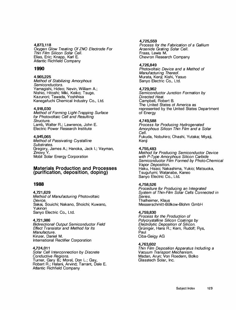
4,873,1 1 8 Oxygen Glow Treating Of ZNO Electrode For Thin Film Silicon Solar Cel/. Elias, Eric; Knapp, Karl E. Atlantic Richfield Company
1 990
4.965,225 Method of Stabilizing Amorphous Semiconductors. Yamagishi, Hideo; Nevin, William A. ; Nishio, Hitoshi; Miki, Keiko; Tsuge, Kazunori; Tawada, Yoshihisa Kanegafuchi Chemical Industry Co., Ltd.
4,918,030 Method of Forming Light-Trapping Surface for Photo voltaic Cel/ and Resulting Structure. Lamb, Walter R.; Lawrence, John E. Electric Power Research Institute
4,945,065 Method of Passivating Crystalline Substrates. Gregory, James A.; Hanoka, Jack I. ; Vayman, Zinovy Y. Mobil Solar Energy Corporation
Materials Production and Processes (purification, deposition, doping)
1988
4,721 ,629 Method of Manufacturing Photo voltaic Device. Sakai, Souichi; Nakano, Shoichi; Kuwano, Yukinori Sanyo Electric Co., Ltd.
4,721 ,986 Bidirectional Output Semiconductor Field Effect Transistor and Method for Its Manufacture. Kinzer, Daniel M. International Rectifier Corporation
4,724,01 1 Solar Cel/ Interconnection by Discrete Conductive Regions. Turner, Gary B.; Morel, Don L. ; Gay, Robert R.; Halani, Arvind; Tarrant, Dale E. Atlantic Richfield Company
4,725,559 Process for the Fabrication of a Gallium Arsenide Grating Solar Cel/. Fraas, Lewis M. Chevron Research Company
4,726,849 Photovoltaic Device and a Method of Manufacturing Thereof. Murata, Kenji; Kishi, Yasuo Sanyo Electric Co., Ltd.
4,729,962 Semiconductor Junction Formation by Directed Heat. Campbell, Robert B. The United States of America as represented by the United States Department of Energy
4,749,588 Process for Producing Hydrogenated Amorphous Silicon Thin Film and a Solar Cel/. Fukuda, Nobuhiro; Ohashi, Yutaka; Miyaji, Kenji
4,755,483 Method for Producing Semiconductor Device with P-Type Amorphous Silicon Carbide Semiconductor Film Formed by Photo-Chemical Vapor Deposition. Haku, Hisao; Nakashima, Yukio; Matsuoka, Tsugufumi; Watanabe, Kaneo Sanyo Electric Co., Ltd.
4,758,526 Procedure for Producing an Integrated System of Thin-Film Solar Cel/s Connected in Series. Thalheimer, Klaus Messerschmitt-B6Ikow-Blohm GmbH
4,759,830 Process for the PrOduction of Polycrystalline Silicon Coatings by Electrolytic Deposition of Silicon. Gruniger, Hans R.; Kern, Rudolf; Rys, Paul Ciba-Geigy AG
4,763,602 Thin Film Deposition Apparatus Including a Vacuum Transport Mechanism. Madan, Arun; Von Roedern, Bolko Glasstech Solar, Inc.
Subject Index 123

4,764,261 Method of Making Improved Photo voltaic Heterojunction Structures. Ondris, Miroslav; Hichler, Marty A. Stem cor Corporation
4,769,107 Process and Apparatus for the Cyclical Manufacture of Silicon Shaped Articles. Helmreich, Dieter; Gessert, Cord; Miller, Hans-Dieter; Zauhar, Helmut; Priewasser, Georg; Schmid hammer, Leonhard Heliotronic Forschungs- und Entwicklungsgesellschaft fur Solarzellen-Grundstoffe mbH
4,769,682 Boron Doped Semiconductor Materials and Method for Producing Same. Yang, Chi C.; Mohr, Ralph; Hudgens, Stephen; Johncock, Annette; Nath, Prem Energy Conversion Devices, Inc.
4,771 ,017 Patterning Process. Tobin, Stephen P.; Spitzer, Mark B. Spire Corporation
4,772,564 Fault Tolerant Thin-Film Photovoltaic Cell Fabrication Process. Barnett, Allen M.; Hall, Robert B. Astrosystems, Inc.
4,773,973 Process for the Production of Polycrystalline Silicon Coatings by Electrolytic Deposition of Silicon. Gruniger, Hans R.; Kern, Rudolf; Rys, Paul Ciba-Geigy AG
4,774,193 Method for Avoiding Shorts in the Manufacture of Layered Electrical Components. Juergens, Wilfried Siemens Aktiengesellschaft
4,774, 194 Process for Manufacturing a Solar Cell Device. Hokuyo, Shigeru Mitsubishi Denki Kabushiki Kaisha
4,777,023 Preparation Of Silicon And Germainum Hydrides Containing Two Different Group 4A Atoms. Fieselmann, Benjamin F. Solarex Corporation
124 U.S. Photovoltaic Patents: 1988 - 1990
4,778,478 Method Of Making Thin Film Photovoltaic Solar Cell. Barnett, Allen M. University of Delaware
4,786,607 Method for Manufacturing A Semiconductor Device Free From Current Leakage Through A Semiconductor Layer. Yamazaki, Shumpei; Suzuki, Kunio; Fukada, Takeshi; Abe, Masayoshi; Kobayashi, Ippei; Shibata, Katsuhiko; Susukida, Masato; Negayama, Susumu; Koyanagi, Kaoru Semiconductor Energy Laboratory Co., Ltd.
4,788,582 Semiconductor Device and Method of Manufacturing the Same. Yamamoto, Hideaki; Seki, Koichi; Tanaka, Toshihiro; Sasano, Akira; Tsukada, Toshihisa; Shimomoto, Yasuharu; Nakano, Toshio; Kanamori, Hideto Hitachi, Ltd.
4,789,641 Method of Manufacturing Amorphous Photo voltaic-Cell Module. Inuzuka, Takahiko Mitsubishi Denki Kabushiki Kaisha
4,794,305 Substrate Support Structure For Ion Implantation Device. Matsukawa, Takyuki Mitsubishi Denki Kabushiki Kaisha
1989
4,806,495 Method of Making Solar Array With Aluminum Foil Matrix. Levine, Jules D.; Jensen, Millard J.; Haney, Ronald E. Texas Instruments Incorporated
4,812,416 Method For Executing A Reproducible Glow Discharge. Hewig, Gerd; Schum, Berthold; Worner, Jorg
4,816,120 Electrodeposited Doped /I-VI Semiconductor Films And Devices Incorporating Such Films. Ondris, Miroslav; Pichler, Marty A.; Brownfield, Richard E. The Standard Oil Company

4,81 8,337 Thin Active-Layer Solar Cell with Multiple Internal Reflections. Barnett, Allen M.; Mauk, Michael G. University of Delaware
4,818,636 Films of Catenated Phosphorus Materials, Their Preparation and Use, and Semiconductor and Other Devices Employing Them. Michel, Christian G.; Schachter, Rozalie; Kuck, Mark A.; Baumann, John A.; Raccah, Paul M. Stauffer Chemical Company
4,822,581 Catenated Phosphorus Materials and Their Preparation. Michel, Christian G.; Schachter, Rozalie; Kuck, Mark A.; Baumann, John A.; Raccah, Paul M. Stauffer Chemical Company
4,828,814 Process for Purification of Solid Material. Sanjurjo, Angel; Pressacco, Sylvia SRI International
4,828,875 Process for the Production of Sintered Films of Cd1 _xZnxS. 1m, Ho-Bin; Park, Kyu-Charn Korea Advanced Institute of Science & Tech.
4,834,062 Multiblade Inner Hole Saw for the Sawing of Crystal Rods Into Thin Blades. Frank, Walter; Palme, Gerhard Wacker Chemitronic
4,834,832 Process And Apparatus For The Manufacture of Silicon Rods. Stock, Horst; Huber, Lothar; Priewasser, Georg Wacker-Chemitronic Gesellschaft fur Elektronik-Grundstoffe mbH
4,845,043 Method for Fabricating Photo voltaic Device Having Improved Short Wavelength Photoresponse. Catalano, Anthony W.
4,849,028 Solar Cell with Integrated Interconnect Device and Process for Fabrication Thereof. Krause, Stanley J. Hughes Aircraft Company
4,865,999 Solar Cell Fabrication Method. Xi, Jianping; Madan, Arun Glasstech Solar, Inc.
4,871 ,517 Apparatus For Parting Wafer-Shaped Silicon Bodies, Useful For Solar Cells, From A Silicon Tape Manufactured In A Horizontal Tape-Drawing Method. Falckenberg, Richard; Hoyler, Gerhard; Grabmaier, Josef Siemens Aktiengesellschaft
4,873,198 Method Of Making Photovoltaic Cell With Chloride Dip. Meyers, Peter V.; Liu, Chung-Heng; Frey, Timothy J. Ametek, Inc.
4,873,202 Solid State Relay And Method Of Manufacturing The Same. Akiyama, Sigeo Matsushita Electric Works, Ltd.
4,874,920 Electronic Device Manufacturing Methods. Yamazaki, Shunpei; Itoh, Kenji; Nagayama, Susumu Semiconductor Energy Laboratory Co., Ltd.
4,876,21 0 Solution Growth Of Lattice Mismatched And Solubility Mismatched Heterostructures. Barnett, Allen M.; Zolper, John C. The University of Delaware
4,876,430 Preweld Test Method. Herschitz, Roman;. Bogorad, Alexander; Harhigh, Robert N. General Electric Company
4,879,251 Method of Making Series-Connected, Thin-Film Solar Module Formed of Crystalline Silicon. Kruehler, Wolfgang; Milia, Peter Siemens Aktiengesellschaft
Subject Index 1 25

1 990
4,891,074 Multiple Cell Photoresponsive Amorphous Alloys and Devices. Ovshinsky, Stanford R.; Adler, David Energy Conversion Devices, Inc.
4,891,325 Method for Reusing Silicon Base Material of a Metal Insulator Semiconductor (MIS) Inversion-Layer Solar Cell. Hezel, Rudolf; Hoffman, Winfried; Schum, Berthold Nukem GmbH
4,894,508 Welder Control System. Glenn, Gregory S. ; Mont jar, William O. Hughes Aircraft Company
4,897,123 Solar Cells and Method for Producing Solar Cells. Mitsui, Kotaro Mitsubishi Denki Kabushiki Kaisha
4,909,863 Process for Levelling Film Surfaces and Products Thereof. Birkmire, Robert W.; McCandless, Brian E. University of Delaware
4,910,153 Deposition Feedstock and Dopant Materials Useful in the Fabrication of Hydrogenated Amorphous Silicon Alloys for Photo voltaic Devices and Other Semiconductor DeVIces. Dickson, Charles R. Solarex Corporation
4,913,199 Arrangement for the Complete Emptying of Quartz Tanks or Crucibles Filled with a Silicon Melt Following Silicon Band Drawing. Falckenberg, Richard; Hoyler, Gerhard; Freienstein, Bernhard; Grabmaier, Josef Siemens Aktiengesellschaft
4,913,744 Solar Cell Arrangement. Hoegl, Helmut; Kern, Ralf M.
4,918,030 Method of Forming Ught-Trapping Surface for Photovoltaic Cell and Resulting Structure. Lamb, Walter R. ; Lawrence, John E. Electric Power Research Institute
126 U.S. Photovoltaic Patents: 1988 · 1 990
4,91 9,913 Process for the Production of Solar Silicon. Kurz, Gunter; Abels, Martin; Schwirtlich, Ingo; Woditsch, Peter Bayer Aktiengesellschaft
4,920,067 Process for 11-VI Compound Epitaxy. Knapp, Jamie
4,927,489 Method for Doping a Melt. Campbell, Robert B.; Kochka, Edgar L.; Piotrowski, Paul A. Westinghouse Electric Corp.
4,940,568 Arrangement for the Continuous Melting of Granulated Silicon for a Band-Drawing Method. Hoyler, Gerhard; Grabmaier, Josef; Falckenberg, Richard; Freienstein, Bernhard Siemens Aktiengesellschaft
4,940,604 Method for Production of Copper Indium Diselenide. Suyama, Naoki; Ueno, Noriyuki; Omura, Kuniyoshi; Takada, Hazime; Kita, Yuutaro; Murozono, Mikio Matsushita Electric Industrial Co., Ltd.
4,950,615 Method and Making Group liB Meta/-Telluride Films and Solar Cells. Basol, Bulent M. ; Kapur, Vijay K. International Solar Electric Technology, Inc.
4,957,772 Method for Forming Functional Deposited Films by Means of Microwave Plasma Chemical Vapor Deposition Method. Saitoh, Keishi; Hashizume, Junichiro; lida, Shigehira; Takei, Tetsuya; Arai, Takayoshi Canon Kabushiki Kaisha
4,962,461 Method for the Reproducable Formation of Material Layers andlor the Treatment of Semiconductor Materials Layers. Meyer, Meinhard; Stormer, Oswald Messerschmitt-Bolkow-Blohm GmbH

4,973,518 Monocrystal Rod Pulled From a Melt. Kida, Michio; Sahira, Kensho; Nozoe, Akikuni Mitsubishi Kinzoku Kabushiki Kaisha
Characterization and Analysis
1988
4,779,980 Atmospheric Optical Calibration System. Hulstrom, Roland L.; Cannon, Theodore W. Midwest Research Institute
1990
4,902,967 Scanning Electron Microscopy by Photo voltage Contrast Imaging. Flesner, Larry D. The United States of America as represented by the Secretary of the Navy
4,924,096 Non-Contact Testing of Photovoltaic Detector Arrays. Mroczkowski, Jacek A.; Reine, Marion B.; Butler, Neal R.
4,956,603 Method and Apparatus for Measuring the Lifetime on P-N Semiconductor Junctions by Photo voltaic Effect. Russo, Vincenzo SGS-Thomson Microelectronics S.r.L.
4,962,461 Method for the Reproducable Formation of Material Layers ' andlor the Treatment of Semiconductor Materials Layers. Meyer, Meinhard; Stormer, Oswald Messerschmitl-Biilkow-Blohm GmbH
COLLECTORS
Flat-Plate Collectors (design, components, productIon)
1 988
4,717,790 Contoured Solar Generator.
Gochermann, Hans Licentia Patent-Verwaltungs GmbH
4,724,010 Solar Cell Module. Okaniwa, Hiroshi; Nakatani, Kenji; Suzuki, Kazutomi Teijin Limited
4,745,078 Method for Integrated Series Connection of Thin Film Solar Cells. Stetler, Walter; Peters, Winfried Siemens Aktiengesellschaft
4,746,618 Method of Continuously Forming an Array of Photo voltaic Cells Electrically Connected in Series. Nath, Prem; Barnard, Timothy Energy Conversion Devices, Inc.
4,749,454 Method of Removing Electrical Shorts and Shunts from a Thin-Film Semiconductor Device. Arya, Rajeewa R.; Oswald, Robert S. Solarex Corporation
4,753,683 Gallium Arsenide Solar Ceff System. Ellion, M. Edmund; Wolff, George Hughes Aircraft Company
4,754,544 Extremely Lightweight, Flexible Semiconductor Device Arrays. Hanak, Joseph J. Energy Conversion Devices, Inc.
4,755,231 Flexible Solar Array Cell and Substrate Therefor. Kurland, Richard M.; Allard, Ira L.; Chaky, Rebecca C.; Inouye, George T. TRW Inc.
4,758,526 Procedure for Producing an Integrated System of Thin-Film Solar Ceffs Connected in Series. Thalheimer, Klaus Messerschmitl-Biilkow-Blohm GmbH
4,769,086 Thin Film Solar Cell with Nickel Back. Tanner, David P.; Jester, Theresa L.; Yin, Ming-Jau Atlantic Richfield Company
Subject Index 127

4,773,943 Photo voltaic Device and a Method of Producing the Same. Yamaguchi, Fuminori; Tomita, Kenji Kyocera Corporation
4,773,944 Large Area, Low Voltage, High Current Photo voltaic Modules and Method of Fabricating Same. Nath, Prem; Laarman, Timothy; Vogeli, Craig; Whelan, Kenneth; Kelly, Bernard Energy Conversion Devices, Inc.
4,783,421 Method For Manufacturing Electrical Contacts For A Thin-Film Semiconductor Device. Carlson, David E.; Dickson, Charles R. ; D'Aiello, Robert V. Solarex Corporation
4,787,580 Large Solar Arrays with High Natural Frequencies. Ganssle, Eugene R. General Electric Company
4,794,027 Process for Coating A Base Material With An Elastomer and Product Produced By Such Process. Hering, Reinhard F.
1 989
303,244 Combined Flexible Solar Cell Panel and Deployment/Storage Mast. Hanak, Joseph J. Energy Conversion Devices, Inc.
4,795,500 Photovoltaic Device. Kishi, Yasuo; Inoue, Hiroshi; Tanaka, Hiroyuki Sanyo Electric Co., Ltd.
4,806,436 Substrate For Amorphous Silicon Solar Cells. Tada, Kiyoshi; Tsukamoto, Kenji; Otsuka, Tatsuo Showa Aluminum Corporation
4,806,495 Method of Making Solar Array With Aluminum Foil Matrix. Levine, Jules D. ; Jensen, Millard J.; Haney, Ronald E. Texas Instruments Incorporated
128 U.S. Photovoltaic Patents: 1988 - 1990
4,808,242 Photovoltaic Device and a Method of Manufacturing Thereof. Murata, Kenji; Kishi, Yasuo San yo Electric Co., Ltd.
4,81 6,324 Flexible Photo voltaic Device. Berman, Elliot Atlantic Richfield Company
4,824,488 Photo voltaic Device. Sakai, Souichi; Kuwano, Yukinori Sanyo Electric Co., Ltd.
4,830,038 Photovoltaic Module. Anderson, A. Jerome; Beze, Norman L. Atlantic Richfield Company
4,832,755 Glass Encapsulation of Solar Cell Arrays to Minimize Voltage/Plasma Interaction Effects in a Space Environment. Barton, John R.; Reiss, Amy C. ; Silverman, Sidney The Boeing Company
4,854,974 Electrical Contacts for a Thin-Film Semiconductor Device. Carlson, David E.; Dickson, Charles R.; D' Aiello, Robert V. Solarex Corporation
4,854,975 Solar Cell with Integrated Interconnect Device and Process for Fabrication Thereof. Krause, Stanley J. Hughes Aircraft Company
4,869,755 Encapsulation of a Photo voltaic Element. Huschka, Hans; Hoffman, Winfried Nukem GmbH
4,872,925 Photo voltaic Cell Fabrication Method and Panel Made Thereby. McMaster, Harold A. Glasstech, Inc.
4,876,430 Pre weld Test Method. Herschitz, Roman; Bogorad, Alexander; Harhigh, Robert N. General Electric Company

4,886,554 Solar Roofing Assembly. Woodring, William J.; Horner Jr., Charles J. GAF Corporation
4,888,061 Thin·Film Solar Cells Resistant to Damage During Flexion. Wenz, Robert P. Minnesota Mining and Manufacturing Company
1 990
4,892,592 Thin Film Semiconductor Solar Cell Array and Method of Making. Dickson, Charles R.; Johnson, Barry J.; Gerhardt, David B. Solarex Corporation
4,900,369 Solar Cell. Hezel, Rudolf; Hackstein, Karl G. Nukem GmbH
4,907,915 Template for Installing Photovoltaic Panel Assembly and Method. Nicholson, Robert D.; Kaake, Steven A.F.; Smith, Robert F. Glasstech, Inc.
4,909,856 Composite Coverglass for Solar Cell. Ralph, Eugene l. Hughes Aircraft Company
4,910,415 Interconnection Between a Battery Cell and a Printed Circuit Board in an Electric Apparatus. Yoshimura, Yutaka Sharp Kabushiki Kaisha
4,913,744 Solar Cell Arrangement. Hoegl, Helmut; Kern, Ralf M.
4,914,044 Method of Making Tandem Solar Cell Module. Grabmaier, Josef; Kruehler, Wolfgang; Endroes, Arthur Siemens Aktiengesellschaft
4,915,745 Thin Film Solar Cell and Method of Making. Pollock, Gary A.; Mitchell, Kim W.; Ermer, James H. Atlantic Richfield Company
4,917,752 Method of Forming Contacts on Semiconductor Members. Jensen, Millard J.; Levine, Jules D. Texas Instruments Incorporated
4,920,917 Reactor for Depositing a Layer on a Moving Substrate. Nakatani, Kenji; Okaniwa, Hiroshi; Yano, Mitsuaki Teijin Limited
4,929,281 Method for Producing Thin-Film Solar Cells in a Series-Connected Array. Worner, Jorg Nukem GmbH
4,931,412 Method of Producing a Thin Film Solar Cell Having a N-I-P Structure. Fischer, Roland; Grabe, Gerhard; Niemann, Ekkehard Licentia Patent-Verwaltungs GmbH
4,933,020 Solar Installation. Wenzel, Joachim
4,935,067 Solar Cell and Fabrication Method Thereof. Sato, Katsumi; Hokuyo, Shigeru; Matsumoto, Hideo Mitsubishi Denki Kabushiki Kaisha
4,936,924 Thin-Film Solar Battery and Its Manufacturing Method. Inuzuka, Takahiko Mitsubishi Denki Kabushiki Kaisha
4,937,651 Semiconductor Device Free from the Current Leakage Through a Semiconductor Layer and Method for Manufacturing Same. Yamazaki, Shunpei; Suzuki, Kunia; Kinka, Mikio; Fukada, Takeshi; Abe, Masayoshi; Kobayashi, Ippei; Shibata, Katsuhiko; Susukida, Masato; Nagayama, Susumu; Koyanagi, Kaoru Semiconductor Energy Laboratory Co., ltd.
Subject Index 129
4,940,496 Solar Battery Device. Matsumoto, Hideo; Sato, Katsumi; Hokuyo, Shigeru Mitsubishi Denki Kabushiki Kaisha
4,942,865 Compound Solar Collector Building Construction. Pierce-Bjorklund, Patricia
4,948,740 Method for the Integrated Series-Interconnection of Thick-Film Solar Cells and Method for the Manufacture of Tandem Solar Cells. Plaettner, Rolf Siemens Aktiengesellschaft
4,953,577 Spray Encapsulation of Photo voltaic Modules. Marshall, Jack Solarex Corporation
4,954,181 . Solar Cell Module and Method of Manufacture.
.
Nishiura, Masaharu; Ichimura, Takeshige; Kamiyama, Michinari Fuji Electric Company Ltd. ; Fuji Electric Corporate Research and Development Ltd.
4,956,023 Integrated Solar Cell Device. Tsuge, Kazunori; Endo, Toshihito; Kobayashi, Kenji; Tawada, Yoshihisa Kanegafuchi Kagaku Kogyo Kabushiki Kaisha
4,956,601 Method of Forming an Array of Apertures in an Aluminum Foil. Levine, Jules D.; Jensen, Millard J. Texas Instruments Incorporated
4,965,655 Interconnected Semiconductor Devices. Grimmer, Derrick P.; Paulson, Kenneth R.; Gilbert, James R. Minnesota Mining and Manufacturing Company
4,966,631 Support for Photo voltaic Arrays. Matlin, Ronald W.; Lenskold, Richard K.; Rangarajan, Anand Chronar Corp.
130 U.S. Photovoltaic Patents: 1988 - 1990
4,968,354 Thin Film Solar Cell Array. Nishiura, Masaharu; Yamada, Katsumi Fuji Electric Co., Ltd.
4,968,372 Method of Producing a Flexible Carrier Substrate. Maass, Heinz Licentia Patent-Verwaltungs GmbH
4,975,133 Apparatus for Welding Components Together with the Use of Ultrasound. Gochermann, Hans Licentia Patent-Verwaltungs GmbH
Concentrator Collectors (design, components, production)
1988
4,746,371 Mechanically Stacked Photo voltaic Cells, Package Assembly, and Modules. McLeod, Paul S.; Cape, John A.; Fraas, Lewis M.; Partain, Larry D. Chevron Research Company
4,748,130 Method of Making Buried Contact Solar Cell. Wenham, Stuart R.; Green, Martin A. Unisearch Limited
4,776,893 GaAs on GaSb Mechanically Stacked Photovoltaic Cells, Package Assembly, and Modules. McLeod, Paul S.; Cape, John A.; Fraas, Lewis M.; Partain, Larry D. Chevron Research Company
4,784,700 Point Focus Solar Concentrator Using Reflector Strips of Various Geometries to Form Primary and Secondary Reflectors. Stern, Tbeodore G.; Cornwall, Mickey; Kaincz, Bela; Mildice, James W. General Dynamics Corp.lSpace Systems Div.
4,789,408 Solar Collector. Fitzsimmons, James W.

1989
4,830,678 Liquid·Cooled Sealed Enclosure for Concentrator Solar Cell and Secondary Lens. Todorof, William J.; Murphy, Mark
4,834,805 Photovoltaic Power Modules and Methods for Making Same. Erbert, Virgil Wattsun, Inc.
4,836,861 Solar Cell And Cell Mount. Peltzer, Douglas L.; Bechtel, Richard L.; Ko, Wen C. ; Liggett, William T. Tactical Fabs, Inc.
4,888,063 Variable Aperture, Variable Flux Density, Aerospace Solar Collector. Powell, Roger A.
1990
4,960,468 Photo voltaic Converter Having Apertured Reflective Enclosure. Sinton, Ronald A.; Swanson, Richard M. The Board of Trustees of the Leland Stanford Junior University
4,971 ,633 Photo voltaic Cell Assembly. Beavis, Leonard C.; Panitz, Janda K.G.; Sharp, Donald J. The United States of America as represented by the Department of Energy
Op.tics and Trackers (lenses, reflectors, tracking devices, and related componenls)
1988
4,730,602 Apparatus for Automatically Directing Solar Radiation Focused by a Reflector. Posnansky, Mario; Posnansky, Hernan
4,771,764 Water-Borne Azimuth-Altitude Tracking Solar Concentrators. Cluff, C. Brent
4,786,795 Sun Tracking Device Floating Upon Liquid Surface. Kurashima, Shozo; Umezawa, Yasuhiko Kyocera Corporation
4,789,408 Solar Collector. Fitzsimmons, James W.
1 989
4,799,778 Fresnel Lens Concentrator. Jebens, Robert W. General Electric Company
4,833,340 Solar Lighting Reflector Apparatus Having Slatted Mirrors and Improved Tracker. Dominguez, Richard L. Solar Lighting Research, Inc.
4,868,379 Photo voltaic Array With Two-Axis Power Maximization Tracking. West, Rick Utility Power Group
1 990
33,208 Photoelectric Conversion Panel and Assembly Thereof. Yamazaki, Shunpei Semiconductor Energy Laboratory Co., Ltd.
4,891 ,075 Photo voltaic Cell Including Wavelength Shifter Comprising Lanthanide Chelate Fluorophores Based on Dihydropyridine Condensation Products. Dakubu, Salifu Golight, Inc.
4,892,593 Solar Trap. Lew, Hyok S.
4,907,864 Macro-Gradient Optical Density Transmissive Light Concentrators, Lenses and Compound Lenses of Large Geometry. Hagerty, James J.; Danziger, Leslie A. John E. Fetzer Foundation
4,933,020 Solar Installation. Wenzel, Joachim
Subject Index 131

4,943,325 Reflector Assembly. Levy, Sheldon L. Black & Veatch, Engineers-Architects
4,960,468 Photovoltaic Converter Having Apertured Reflective Enclosure. Sinton, Ronald A.; Swanson, Richard M. The Board of Trustees of the Leland Stanford Junior University
4,964,713 Concentrator Arrangement. Goetzberger, Adolf Fraunhofer-Gesellschaft zur Forderund der Forschung E. V.
4,968,355 Two-Axis Tracking Solar Collector Mechanism. Johnson, Kenneth C.
4,975,816 Lens for Low Light Level Lamp. Frost, John S.; Erickson, Mark R. ; Seegan, Kimberly E.; Felder, Bethanne; Wallace, Lloyd V. Siemens Solar Industries
SYSTEMS
Utilitv-Interactive Systems and Interface Technologies (power conditioning) .
1988
4,725,740 DC-AC Converting Arrangement for Photovoltaic System. Nakata, Yukihiko Sharp Kabushiki Kaisha
4,775,865 Emergency Vehicle Warning And Traffic Control System. Smith, Michael R.; Davidson, J. Paul; Pfister, Henry L. E-Lited Limited, A California Limited Partnership
132 u.S. Photovoltaic Patents: 1988 - 1990
4,781 , 1 1 9 Solar-Rapid Mass Transit System. Davis, James G.
1 989
4,819,121 Security Apparatus for Power Converter. Saito, Suzuo; Higaki, Shigetoshi Kabushiki Kaisha Toshiba
4,823,928 Electronic Parking Meter System. Speas, Gary W. POM, Incorporated
4,827,206 Solar Power System For Electronic Parking Meter. Speas, Gary W. POM, Incorporated
4,888,702 Photovoltaic System Controller. Gerken, Kenneth F. Integrated Power Corporation
1 990
H855 Optical Beam Switching Circuit for Photo voltaic Energy Conversion. Otto, William F.; Milton, Richard D.; Jordan, Debbee J. The United States of America as represented by the Secretary of the Army
4,91 6,382 System for Maximizing Efficiency of Power Transfer. Kent, William A. Horner Equipment of Florida, Inc.
4,91 8,357 Combination Incandescent and Solar-Electric Light Bulb with Automatic Switching Device and Charging Means Therefor. Waterbury, Nelson J.
4,958,575 Transit Vehicle Apparatus and Method for Solar Induction Monorails. Antosh, Mark J.
4,972,094 Lighting Devices with Quantum Electric/Light Power Converters. Marks, Alvin M.

4,974,126 Lamp With Power Source Supply For Fan. Hwang, Feng-Lin
Utility· Independent Systems and Storage Technologies
1 988
4,71 8,185 Modular Solar Generating System. Conlin, Kevin l.; Cantrell, Michael P. Solar Signage, Inc.
4,71 9,346 Optical Position Locating Apparatus with Bidirectional Light Transmission. Taillebois, Jacques; Renaud, Jean-Marie; Perrot, Jean-Claude; Gambs, Paul M.C.B.
4,726,044 Writing Instrument with Solar-Powered Electronic Counting and Liquid Crystal Display. Perna, Fred P.; Peterson, Stuart R. Fred P. Perna
4,730,1 1 5 Transformer System and Direct Current Power Supply. Abe, Kozo Logical Co., Ltd.
4,737,712 Isolated Power Transfer and Patient Monitoring System with Interference Rejection Useful with NMR Apparatus. Stormont, Robert S.; Buchwald, Randall H.; Hashoian, Ralph S. General Electric Company
4,739, 163 Position Locating Optical Coder Utilizing Optical Fiber. Gambs, Paul; Taillebois, Jacques; Renaud, Jean-Marie; Perrot, Jean-Claude M.C.B.
4,740,431 Integrated Solar Cell and Battery. Little, Roger G. Spire Corporation
4,744,430 Solar Powered Golf Cart. McCoy, Thomas R.
4,749,982 Intelligent Card. Rikuna, Kenji; Nakano, Harumi; Kara, Kazuya; Shigenaga, Yoshimi; Bito, Hiroyasu; Takeuchi, Eiichi; Tamiya, Morito Casio Computer Co., Ltd.
4,750,099 Circuit for Charging Capacitors. Inoue, Yuichi; Ohtawa, Shuji; Ochiai, Hitoshi; Kiyono, Yoshihiko; Nakamura, Chiaki Seiko Instruments, Inc.
4,751,622 Solar Powered Construction Light. Williams, Lloyd E. Power Plus, Inc.
4,754,271 Liquid Crystal Photograph. Edwards, Willie
4,754,418 Combined Electronic Calculator and Credit Card. Hara, Kazuya Casio Computer Co., Ltd.
4,755,804 System for Feeding and Controlling Low Intensity Obstruction Lights. Levati, Aldo; Siviero, Pietro Telettra Telefonia Elettronica e Radio S.p.A.
4,760,564 Analog Electronic Timepiece with Charging Function. Odagiri, Hiroshi Seiko Instruments, Inc.
4,760,918 Pocketbook Type Electronic Apparatus. Washizuka, Isamu; Tanimoto, Akira Sharp Kabushiki Kaisha
4,760,954 Auxiliary Equipment for the Thermostatic Valve of a Radiator. Hansen, Allan H. Danfoss AlS
4,763,126 Mooring Location System. Jawetz, Ira
Subject Index 133

4,763,310 Bectronic Clock with Solar Cell and Rechangeable Battery. Goetzberger, Adolf Fraunhofer·Geselischaft zur Forderung
4,764,850 Solar-Powered Display Device. Albanese, Philip
4,764,910 Bectronic Timepiece. Ichikawa, Shingo Citizen Watch Co., Ltd.
4,765,623 Talking Crystal Ball Toy. Cardillo, Gary J.; Cahill, Douglas R.
4,771 ,556 Sport Shoe with Melody Emitting Device. Kim, Young J. Samwha Co.
4,772,990 Solar Powered Warning Flasher. Linehan, Dave M.; Zaderej , Victor V.; Hahs, Jr., Charles A. CNI
4,775,800 Power· Supply Apparatus. Wood, Peter Westinghouse Electric Corp.
4,778,378 Self-Powered Intermittent Ignition And Control System for Gas C(jmbustion Appliances. Dolnick, Earl M. ; Goldstein, Mark K. Quantum Group, Inc.
4,782,432 Multi-Function Light. Coffman, Stephen L. ME Generations Inc.
4,782,617 Water Temperature Measurement Apparatus. Peikin, Aaron J. None
4,782,628 Gate Opening Apparatus. Gaddis, John J.
134 U.S. Photovoltaic Patents: 1988 · 1 990
4,783,799 Electronic Communications And Control System. Maass, Joachim A.
4,784,215 Thermal Insulating Shades. Sing, Peter
4,785,226 Powder Supply Device With Solar Cell. Fujisawa, Hidetaka; Wakita, Katsuhiro Casio Computer Co., Ltd.
4,785,435 Self-Chargeable Bectronic Timepiece with Operating Voltage Checking. Inoue, Yuichi; Nakamura, Chiaki; Ohtawa, Shuji; Masaki, Hiroyuki Seiko Instruments, Inc.
4,785,436 Photovoltaic Electronic Timepiece. Sase, Masahiro Citizen Watch Co., Ltd.
4,786,851 Battery Charger. Fuji, Sadao; Yamawski, Takeharu; Takamatsu, Osamu; Kuwamura, Shinji; Suenobu, Kazuhiro; Nakano Hiroshi Kanegafuchi Kagaku Kogyo Kabushiki Kaisha
4,787,167 Apparatus Artificial Fishing Lures Having Variable Characteristics. Wrociawski, Michel T.
4,788,904 Assembly for Cooling Vehicle Parts. Radtke, Wolfgang Siemens Aktiengesellschaft
4,791,413 Soil Moisture Detector With Light Activated Audio Alarm Inhibitor. Lyczek, Kazimierz E.
4,791,621 Solar Cell Powered Clock Having A Decorative Pendulum. Wild, Gerhard; Haller, Edgar Junghans Uhren GmbH
4,794,305 Substrate Support Structure For Ion Implantation Device. Matsukawa, Takyuki Mitsubishi Denki Kabushiki Kaisha

1 989
4,794,715 Motor-Driven Map Holder. Cherwin, Charles
4,796,370 Numerical Display Module. Chang, Kwangling
4,797,535 T ungsten·Halogen Heater. Martin, Wayne A.
4,800,803 Ventilation Device. Farmont, Rolf Farmont Production GmbH & Co., KG
4,804,858 Power Supply Circuit For A Diode Adapted To Emit Light In Dependence Of The Prevailing Surrounding Light. Jorlov, Richard; Nystrom, Lars; Lewenhaupt, Sixten Aimpoint AB
4,806,095 Fuel Valve Control System. Goldstein, Mark K.; Dolnick, Earl M. Quantum Group, Inc.
4,806,855 System For Rating Electric Power Transmission Lines and Equipment. Davis, Murray W.
4,807,686 Shade System. Schnebly, John; Marusak, Thomas J. Comfortex Corporation
4,808,904 Portable Photovoltaic Battery Recharger. Ricaud , Alain M.; Artigliere, Fiore Solarex Corporation
.
4,809,458 Self-Luminous Buoy. Tanikuro, Hideo; Nagamatsu, Kimiaki Nichimo Co., Ltd.
4,811,694 Bird Feeder With Scale. Holmquist, Melvin L.
4,823,241 Portable Solar Charged Operated Lamp Having Orientation Switch For Selectively Energizing Lamp Based Upon Its Physical Orientation. Trattner, Burton Harvey-Westbury Corp.
4,823,928 Electronic Parking Meter System. Speas, Gary W. POM, Incorporated
4,827,206 Solar Power System For Electronic Parking Meter. Speas, Gary W. POM, Incorporated
4,827,246 Hydrocarbon and Water Level Sensor System Used To Monitor Underground Storage Sites. Dolan, James P. ; Dolan, Patrick M.
4,827,534 Sun-Powered Vest. Haugen, Alvin E.
4,827,645 Illuminated Trash Receptacle. Stamps, Jr., William E. Clean Scene Advertising, Inc.
4,830,606 Gas Lamp and Control Thereof. Dillinger, Bill R.
4,833,697 Writing Instrument for Electronic Counting and Gravity Switch Reset. Perna, Fred P.; Peterson, Stuart R. Fred P. Perna
4,835,664 Solar Lighting Device For Garden Or Driveway. Wen, Hung-Sheng
4,835,918 Device for Shading Spaces. Dippel, Hans-Jurgen MWB Messwandler-Bau AG
4,836,012 Gas Sensor. Daly, Mitchell E.; Schmidt, Ferenc J. Ametek, Inc.
Subject Index 135

4,836,786 Demonstration Calculator. Wong, Robert P. Joseph Leeb Enterprises, Inc.
4,839,039 Automatic Flow-Control Device. Parsons, Natan E.; Novak, Joel S. Recurrent Solutions Limited Partnership
4,839,106 Portable Misting Fan. Steiner, Gregory Gregory A. Steiner
4,839,833 Programmable Display Engineering Scale. Parhiskari. Mustafa
4,841,157 Optical Backscatter Turbidimeter Sensor. Downing, Jr., John P.
4,841,278 Self-lIIuminant Delineator And Delineator System By Use Thereof. . Tezuka, Hirofumi; Nogami, Kouji; Koyano. Toshihide Kyocera Corporation
4,841 ,41 6 Solar Charging Lamp. Doss, Todd
4,843,525 Solar Powered Yard Marker. Williams, Lloyd E. Power Plus, Inc.
4,847,546 Solar Panel Output Enhancement Circuit. Bobier, Joseph A.; Brown, Gerald E. Bobier Electronics, Inc.
4,851,308 Solid-State Energy Storage Cell Wherein The Electrolyte Comprises An Organic Support And An Inorganic Salt. Akhtar, Masud Chronar Corp.
4,856,605 Nonsystem-Connected Electronic Balance. Cornelius. Klaus; Exner, Rainer Sartorius GmbH
4,864, 100 Controlled Zone Defrosting System. Cicak, Michael J. Glasstech International, loP.
136 U.S. Photovoltaic Patents: 1 988 · 1990
4,864,763 Temperature Measurement Apparatus for Use in Recreational and Sporting Activities. Peikin, Aaron J.
4,867, 191 Solar Activated Gas Light Control Module. Walters, Jon S. American General Products, Inc.
4,868,376 Intelligent Portable Interactive Personal Data System. Lessin. Arlen R.; Gruppuso, Frank M.; Harrison. Shelley A. SmartCard International Inc.
4,871,042 Electric Bicycle. Hsu, Chi-chu; Yu, Chin-ching; Chao, Suyueh; Huang, Miguel C.J.
4,871 ,959 Solar Trickle Charger for Lead Acid Batteries. Gali, Carl E.
4,872,149 Electronic Advertising System for Solar Powered Parking Meter. Speas, Gary W. POM, Incorporated
4,872,679 Combination Table Top Football And Hockey Game. Bohaski, Frank lo; Horner, Jr .• Jack lo
4,873,790 Plant Spinner. Laterza, Joseph
4,875,031 Vapor Monitoring System. Filippi, Ernest A.; Miller. Kenneth lo
4,878,043 Device for Indicating Hydroculture-Related Values. Heusquin. Guy; Heusquin, Anke
4,879,760 Optical Fiber Transmissive Signal Modulation System. Kroll, Mark W.; Pommrehn, Mark R. Cherne Medical, Inc.

4,882,239 Light-Rechargeable Battery. Grimmer, Derrick P.; Wenz, Robert P. Minnesota Mining and Manufacturing Company
4,882,471 Electronic Equipment Using A Cover. Kai, Tomoko Canon Kabushiki Kaisha
4,884,017 Solar Powered Construction Light. Williams, Lloyd E. Power Plus, Inc.
4,890,093 Solar Powered Proximity Triggered Light. Allison, James R.; Bolin, Garry J . Schlage Lock Company
1990
307,032 Electronic Calculator with Solar Cell. Sawada, Masaji; Takahashi, Toshiya Sharp Corporation
308,693 Electronic Calculator with Solar Cell. Sakaguchi, Hiroshi; lida, Katsuhiro Sharp Corporation
309,747 Electronic Calculator with Solar Cel/. Sakaguchi, Hiroshi; Saimen, Tadahiko Sharp Corporation
31 0,093 Electronic Calculator with Solar Cel/. Sakaguchi, Hiroshi; lida, Katsuhiro Sharp Corporation
4_942,629 Ski Goggles with Heated Lens. Stadlmann, Gunter Optyl Eyewear Fashion International Corporation
4,893,356 Air Conditioned Headwear Having Convertible Power Module. Waters, William A.
4,896,305 Animal Luring Device. Gimbal, Eric A.
4,896,452 Solar Powered Bait Box. Smith, Harry D.; Sapp, Fletcher D.
4,898,531 Photosensitive Control of Electrically Powered Emissive Ignition Devices. Goldstein, Mark K.; Dolnick, Earl M. Quantum Group, Inc.
4,899,044 Optically Coupled Remote Sensor Apparatus and System. Hansen, J. Richard; Asars, Juris A.; Oates, Robert M. Westinghouse Electric Corp.
4,899,645 Solar Powered Ventilator. Wolfe, Philip R.; Callaghan, John K.; Pidgeon, Simon Intersolar Ltd.
4,900,432 Pool Surface Cleaner. Arnold, Aaron L.; Woodward, Daniel A.
4,901,295 Device Comprising a Solar Cell for Winding a Barrel Spring. Taguezout, Daho; Xuan, Mai T. Asulab SA
4,903,1 72 Display Construction. Sch6niger, Karl-Heinz; Scheid, Winfried
4,904,998 Lighting Peg with Variable Pulsation Rate. Niimi, Kikuo Kictec Incorporation
4,905,579 Radon Gas Ventilation Pump System and Method. Dame, Richard E.
4,906,178 Self-Powered Gas Appliance. Goldstein, Mark K.; Dolnick, Earl M.; Bass, John C. Quantum Group, Inc.
4,91 1 ,257 Vehicle Having a Solar Battery System. Kajimoto, Shinshi; Niitani, Tooru;. Michihara, Osamu; Kuroiwa, Mitsutoshi Mazda Motor Corporation
Subject Index 137

4,916,296 Light Modulating Smart Card. Streck, Donald A. Jerry R. Iggulden
4,922,088 Automatic Solar Lighting Apparatus Having a Solar Following Sensor. Kasuya, Satoshi Technology Network, Inc.
4,925,335 Prefabricated Continuous Roadmarking Tape Having Optical and Electromagnetic Function. Eigenmann, Ludwig
4,929,842 Electro-Optical Measuring and Transmission Device Using Overload and Overvoltage Protection Circuits. ter Hasebrg, Jan l.; Nedwig, Joachim; Kruse, Klaus-Dieter Licentia Patent-Verwaltungs GmbH
4,929,942 Lighting Peg. Niimi, Kikuo Kictec Incorporation
4,933,618 Chair for Sunbathing. Ortlieb, Johann F.
4,934,338 Method and Apparatus for Preheating Ventilation Air for a Building. Hollick, John C.; Peter, Rolf W. Solarwall International Limited
4,935,742 Automatic Radar Generator. Marin, Jonathan
4,936,043 Live Bait Container Incorporating Aerator and Power Supply. Steele, John J.
4,939,986 Exhaust Ventilator. Turner, Charles R. John C. Garvin, Jr. and Harold W. Hilton
4,942,723 Solar Powered Lawnmower. Wassell, Stephen R.
138 U.S. PhOlovoltaic Patents: 1988 · 1990
4,955,982 Raised Depressible Pavement Marker. Paulos, Harry D. Olympic Machines, Inc.
4,959,603 Solar Battery Equipment. Yamamoto, Shigeo; Noda, Toshio Osaka Titanium Co., Ltd.
4,963,811 Method and Apparatus for Powering Electrical and Electronic Consuming Devices with Solar Energy. Weber, Hans R.
4,967,895 Parameter Control System for Electronic Parking Meter. Speas, Gary W. POM, Incorporated
4,970,453 Solar Charging System for an IC Card Having Voltage Current Regulation. Oogita, Yoshinori Sharp Kabushiki Kaisha
4,975,584 Method and Apparatus for Collecting, Processing and Displaying Ultraviolet Radiation Data. Benjamin, Thomas l.; Robillard, Jean J . Mountain Ocean, Ltd.
4,975,816 Lens for Low Light Level Lamp. Frost, John S.; Erickson, Mark R.; Seegan, Kimberly E.; Felder, Bethanne; Wallace, Lloyd V. Siemens Solar Industries
4,980,574 Solar Irrigation D.C. to A.C. Power System Supplying A. C. Voltage at a Precise Power Frequency. Cirrito, William J. Photocomm, Inc.

PV-Hybrid Systems (PV-thermal, photoelectrochemical) 1988
4,730,602 Apparatus for Automatically Directing Solar Radiation Focused by a Reflector. Posnansky, Mario; Posnansky, Hernan
4,746,370 Photothermophotovoltaic Converter. Woolf, Lawrence D. GA Technologies, Inc.
4,751,413 Solar Energy Motor. Izawa, Hideo Sharp Kabushiki Kaisha
4,768,738 Flexible Solar Skin in Combination with an Airplane. Weinert, Friedrich
4,771,763 Solar Powered Fluid Heating System. Wetzel, Jr., Otto K. Wetzel Enterprises, Inc.
4,771,764 Water-Borne Azimuth-Altitude Tracking Solar Concentrators. Cluff, C. Brent
4,776,895 Multiband Emitter Matched to Multilayer Photo voltaic Collector. Goldstein, Mark K. Quantum Group, Inc.
4,784,215 Thermal Insulating Shades. Sing, Peter
4,784,700 Point Focus Solar Concentrator Using Reflector Strips of Various Geometries to Form Primary and Secondary Reflectors. Stern, Theodore G.; Cornwall, Mickey; Kaincz, Bela; Mildice, James W. General Dynamics Corp.lSpace Systems Div.
4,793,799 Photovoltaic Control System. Goldstein, Mark K.; Dolnick, Earl M. Quantum Group, Inc.
1989
4,797,535 Tungsten-Halogen Heater. Martin, Wayne A.
4,830,677 Solar Generator. Geisler, Jr., Herbert A.
4,836,862 Thermophotovoltaic System. Pelka, David G. ; Popovich, John M.; Fleishman, Roc V.
4,841,731 Electrical Energy Production Apparatus. Tindell, Gene Electrical Generation Technology, Inc.
4,841,946 Solar Collector, Transmitter and Heater. Marks, Alvin M.
4,860,509 Photo voltaic Cells In Combination With Single Ply Roofing Membranes. Laaly, Heshmat 0.; Stevenson, Edward J.
4,885,995 Solar Induction Monorail System and Method of Using. Antosh, Mark J.
4,888,063 Variable Aperture, Variable Flux Density, Aerospace Solar Collector. Powell, Roger A.
1990
4,892,593 Solar Trap. Lew, Hyok S.
4,898,531 Photosensitive Control of Electrically Powered Emissive Ignition Devices. Goldstein, Mark K.; Dolnick, Earl M. Quantum Group, Inc.
4,906,178 Self-Powered Gas Appliance. Goldstein, Mark K.; Dolnick, Earl M.; Bass, John C. Quantum Group, Inc.
4,91 0,963 Solar Energy Process. Vanzo, Gordon F.
Subject Index 1 39

4,916,035 Photoelectrochemical Cel/s Having Functions as a Solar Cel/ and a Secondary Cel/. Yamashita, Akio; Sekido, Satoshi; Takeda, Takeshi; Tsuchiya, Sohji Matsushita Electric Industrial Co.
4,91 8,357 Combination Incandescent and Solar-Electric Light Bulb with Automatic Switching Device and Charging Means Therefor. Waterbury, Nelson J.
4,934,338 Method and Apparatus for Preheating Ventilation Air for a Building. Hollick, John C.; Peter, Rolf W. Solarwall International Limited
4,946,512 Solar Energy Col/ector Device. Fukuroi, Takeo; Yoshida, Shinichirou; Ohmura, Akira Yoshida Kogyo K. K.
4,956,877 Optical Fiber Reflective Signal Modulation System. Kroll, Mark W.; Pommrehn, Mark R. Cherne Medical, Inc.
4,964,793 Solar Induction Monorail Fabrication Apparatus. Antosh, Mark J.
4,976,606 Thermophotovoltaic Technology. Nelson, Robert E. TPV Energy Systems, Inc.
Systems SUPP'ort (testing, maintenance operation, ani:l control)
1988
4,742,291 Interface Control for Storage Battery Based Alternate Energy Systems. Bobier, Joseph A.; Brown, Gerald E. Bobier Electronics, Inc.
140 U.S. Photovoltaic Patents: 1 988 - 1990
4,775,800 Power-Supply Apparatus. Wood, Peter Westinghouse Electric Corp.
4,775,923 Inverter For Converting A Direct Voltage Into An Alternating Voltage. Schmid, Jurgen; Schatzle, Rainer Fraunhofer-Gesellschaft zur Forderung der angewandten Forschung e V.
4,792,749 Power Source Voltage Detector Device Incorporated in LSI Circuit. Kitagawa, Nobutaka; Ito, Makoto Kabushiki Kaisha Toshiba
4,793,799 Photovottaic Control System. Goldstein, Mark K.; Dolnick, Earl M. Quantum Group, Inc.
1 989
303,244 Combined Flexible Solar Cel/ Panel and Deployment/Storage Mast. Hanak, Joseph J. Energy Conversion Devices, Inc.
4,812,737 Voltage Regulator For Solar Cel/ Arrays. Fleck, Gerald W. TRW Inc.
4,81 9,121 Security Apparatus for Power Converter. Saito, Suzuo; Higaki, Shigetoshi Kabushiki Kaisha Toshiba
4,846,425 Method and Apparatus for Atomic Beam Irradiation. Champetier, Robert J. Hughes Aircraft Company
4,847,546 Solar Panel Output Enhancement Circuit. Bobier, Joseph A.; Brown, Gerald E. Bobier Electronics, Inc.
4,851,308 Solid-State Energy Storage Cell Wherein The Electrolyte Comprises An Organic Support And An Inorganic Salt. Akhtar, Masud Chronar Corp.

4,868,379 Photovoltaic Array With Two-Axis Power Maximization Tracking. West, Rick Utility Power Group
4,873,480 Coupling Network for Improving Conversion Efficiency of Photo voltaic Power Source. Lafferty, Donald L.
1 990
4,963,81 1 Method and Apparatus for Powering Electrical and Electronic Consuming Devices with Solar Energy. Weber, Hans R.
Subject Index 141

142 U.S. Photovoltaic Patents: 1988 - 1 990 *U,S. GOVERNMENT PRINTING OFFICE: 1992-312-687165609