university of vaasa faculty of technology automation
TRANSCRIPT
UNIVERSITY OF VAASA
FACULTY OF TECHNOLOGY
AUTOMATION TECHNOLOGY
Kim Berg
EVALUATION OF SYSTEMVERILOG AND CONSTRAINED RANDOM
VERIFICATION FOR DIGITAL DESIGNS
Vaasa 2018
Supervisor Jarmo Alander
Instructor Petri Ylirinne

2
FOREWORD
The purpose of this thesis was to evaluate verification methods for Field Programmable
Gate Arrays with an aim to improve the testing of digital designs at Danfoss Drives. I
want to thank the supervisor of this thesis, professor Jarmo Alander, and the instructor,
MSc Petri Ylirinne, for providing valuable guidance and support throughout the process
of writing this study.

3
TABLE OF CONTENTS
FOREWORD 2
TABLE OF CONTENTS 3
1 INTRODUCTION 9
2 THEORY AND BACKGROUND 12
3 VERIFICATION CONCEPTS OF THIS STUDY 17
3.1 Constrained Random Verification and Coverage Driven Verification 17
3.1.1 The Hardwave Verification Language features of SystemVerilog 18
3.1.2 Transaction Level Modeling 19
3.1.3 The Universal Verification Methodology 20
3.1.4 Self-checking test benches 24
3.2 Temporal Logic verification 28
3.2.1 SystemVerilog Assertions 29
3.2.2 Assertions used as protocol checkers 32
3.2.3 Using assertions to complement test benches 32
4 PRESENT TESTING METHODS OF THE COMPANY 34
4.1 Simulation-based test types in use 34
4.2 Verification methods in use 35
4.3 Test reporting with code coverage 36
5 VERIFICATION STRATEGY 39
5.1 Verification strategies for the IP-block test 39
5.1.1 Full IP test bench 40
4
5.1.2 Divide and conquer test bench 43
5.2 Verification strategy for the integration test 44
5.3 Functional coverage 47
6 CASE STUDIES 48
6.1 Testing the Discrete Root Mean Square and Spectrum Analyser co-processing
IP 48
6.1.1 Functional description of the IP 48
6.1.2 The verification plan 50
6.1.3 The full IP test bench 53
6.1.4 Test cases of the full IP test bench 53
6.1.5 Building the full IP test bench 55
6.1.6 Building the divide and conquer test benches 66
6.2 Testing the priority arbitrated full-duplex communication SUT 71
6.2.1 Functional description of the SUT 72
6.2.2 The verification plan 74
6.2.3 Building the NBNA-test 76
7 RESULTS 84
7.1 Results of the full IP test bench case study 84
7.2 Results of the divide and conquer method 87
7.3 Results of the system level test case study 91
8 CONCLUSIONS 93
LIST OF REFERENCES 98

5
SYMBOLS AND ABBREVIATIONS
MHz Megahertz
ms
ABV
Millisecond
Assertion Based Verification
AC
AD
Alternating Current
Analog to Digital
ADC Analog to Digital Converter
ALU Arithmetic Logic Unit
ASIC Application Specific Integrated Circuit
AXI Advanced Extensible Interface
BFM Bus Functional Model
CDV Coverage Driven Verification
CRV Constrained Random Verification
DC Direct Current
DMA Direct Memory Access
DRMS Discrete Root Mean Square
DUT Design Under Test
FEC Focused Expession Coverage
FIFO First In First Out
FPGA Field Programmable Gate Array
FSM Finite State Machine
6
HDL Hardware Description Language
HVL Hardware Verification Language
IP Intellectual Property
MMUR Memory Mapped User Register
OOP Object-Oriented Programming
PSL Property Specification Language
PWM Pulse Width Modulation
RTL Register Transfer Level
SA Spectrum Analyser
SoC System on a Chip
SUT System Under Test
SVA
TDD
SystemVerilog Assertions
Test Driven Development
TLM Transaction Level Modeling
UVM Universal Verification Methodology
VFD Variable Frequency Drive
VIF Virtual Interface
VIP Verification Intellectual Property
VHDL Very High Speed Integrated Circuit Hardware Description
Language
7
UNIVERSITY OF VAASA
Faculty of technology
Author: Kim Berg
Topic of the Thesis: Evaluation of SystemVerilog and Constrained Ran-
dom Verification for Digital Designs
Supervisor: Professor Jarmo Alander
Instructor: MSc Petri Ylirinne
Degree: Master of Science in Technology
Major of Subject: Automation Technology
Year of Entering the University: 2012
Year of Completing the Thesis: 2018 Pages: 100
The Field Programmable Gate Array is a device that consists of configurable logic, on
chip-memory and often functionality that is fixed into silicon, such as hardware multi-
pliers or transceivers for peripheral communication. The Field Programmable Gate Ar-
ray is a configurable and reprogrammable digital circuit that can be designed to imple-
ment functionality that is deterministic and parallel. Due to these qualities the Field
Programmable Gate Array is also an energy efficient choice of hardware for many digi-
tal designs.
Technological advancements in the semiconductor industry have resulted in a continu-
ous decrease in transistor sizes, which in turn has allowed for an increased transistor
density in semiconductor devices. For Field Programmable Gate Arrays the develop-
ment has led to increasingly complex designs, as an increased amount of programmable
resources are available. Consequently, the time and effort spent in verification of the
digital designs has increased. Discovering design flaws before end products are released
is not only economically crucial, but a failure to do so might damage the reputation of a
company. In this thesis current verification trends are evaluated in three case studies
made for Danfoss Drives. The objective of the thesis is to determine whether the quality
of testing of Field Programmable Gate Array designs at the company can be improved
by using Constrained Random Verification and the SystemVerilog language. Test
benches for behavioral simulations are built using SystemVerilog in conjunction with
the Universal Verification Methodology.
Constrained Random Verification based on the SystemVerilog language and the Uni-
versal Verification Methodology was evaluated for unit level testing in two case studies
for one Intellectual Property core. A third case study was made for a system level design
of multiple Intellectual Property cores as a SystemVerilog test bench utilizing neither
constrained randomization nor the Universal Verification Methodology. Improved test
coverage and an increased degree of automatization was achieved for the unit level test-
ing, although at the cost of an increased verification effort. In the system level testing
the capabilities of the SystemVerilog language proved beneficial, especially for creating
transaction level stimulus, writing self-checking mechanisms for the test bench and
modularizing its structure.
KEYWORDS: Field Programmable Gate Array, Verification, Constrained Ran-
dom Verification, SystemVerilog, The Universal Verification Methodology

8
VAASAN YLIOPISTO
Teknologian ja innovaatiojohtamisen yksikkö
Tekijä: Kim Berg
Diplomityön nimi: SystemVerilogin ja Painotetun
Satunnaistamistestauksen Arviointi Digitaalipiireille
Valvoja: Professori Jarmo Alander
Ohjaaja: DI Petri Ylirinne
Tutkinto: Diplomi-insinööri
Pääaine Automation Technology
Opintojen aloitusvuosi: 2012
Diplomityön valmistumisvuosi: 2018 Sivumäärä: 100
Field Programmable Gate Array on laite joka koostuu ohjelmoitavasta logiikasta,
sisäisestä muistista ja usein myös toiminnallisuudesta joka on kiinteästi sidottu
laitteistoon, kuten kertolaskupiirit tai lähetin-vastaanotimmet ulkoista viestintää varten.
Field Programmable Gate Array on konfiguroitava ja uudelleenohjelmoitava
digitaalinen piiri joka voidaan suunnitella toteuttamaan toiminnallisuutta joka on
determinististä ja rinnakkaista. Näistä ominaisuuksista johtuen, Field Programmable
Gate Array on myös energiatehokas laitteistovalinta monen digitaalipiirin
mallinnukseen.
Tekninen kehitys puolijohdeteollisuudessa on johtanut jatkuvaan transistorikokojen
pienenemiseen, mikä puolestaan on sallinut suuremman transistoritiheyden
puolijohdelaitteissa. Piireille mahtuvien resurssien kasvaessa myös Field Programmable
Gate Array laitteiden mallit ovat monimutkaistuneet. Tästä johtuen, suunniteltujen
digitaalipiirien verifiointiin kuluva aika ja vaiva on kasvanut. Suunnitteluvirheiden
löytäminen tuotteesta ennen sen julkistamista ei ole valmistajalle ainoastaan
taloudellisesti tärkeää, vaan saattaa epäonnistuessaan myös olla haitaksi valmistajan
maineelle. Tässä tutkimuksessa ajankohtaisia verifiointitrendejä on arvioitu kolmessa
Danfoss Drivesille toteutetussa tapaustutkimuksessa. Tutkimuksen tavoitteena on
arvioida Painotetun Satunnaistamistestauksen ja SystemVerilog-kielen hyödyn Danfoss
Drivesille toteutettujen Field Programmable Gate Array mallien verifioinnissa.
Käyttäytmissimulointeja varten mallinnetut testipenkit toteutetaan SystemVerilog-
kielellä käyttäen metodologiana Universal Verification Methodologya.
SystemVerilogiin ja Universal Verification Methodologyyn pohjautuvaa Painotettua
Satunnaistamistestausta on arvioitu yksikkötestaukselle kahdessa tapaustutkimuksessa
yhdelle Intellectual Property lohkolle. Kolmas tapaustutkimus on toteutettu
järjestelmätason testaukselle useamman Intellectual Property lohkon järjestelmälle
ilman painotettua satunnaistamista tai Universal Verification Methodologya.
Yksikkötason testauksessa testikattavuuksia onnistuttiin kohottamaan ja
testiautomaation aste kasvoi. Verifiointiin panostettu aika kuitenkin kasvoi.
Järjestelmätason testauksessa SystemVerilogin kieliominaisuudet osoittautuivat
hyödylliseksi, etenkin transaktiotason testisyötteen kirjoittamisessa, automaattisessa
vasteentarkistuksessa ja testipenkin modulaarisen rakenteen mallintamisessa.
KEYWORDS: Field Programmable Gate Array, Verifiointi, Painotettu Satunnais-
tamistestaus, SystemVerilog, The Universal Verification Methodology

9
1 INTRODUCTION
The Field Programmable Gate Array, or FPGA, is a digital circuit that contains configu-
rable logic blocks, on-chip memory and often functionality that is fixed into silicon,
such as hardware multipliers or transceivers for peripheral communication. The config-
urable logic of the FPGA can be designed to implement functionality that is determinis-
tic and parallel. As a result of this parallelism, FPGAs can achieve high throughput for
data handling in tasks such as digital signal processing. An essential feature of the
FPGA is that it is not only configurable, but also reconfigurable. Compared to conven-
tional integrated circuit architectures, such as the Application Specific Integrated Circuit
(ASIC), the FPGA offers a solution that is cheaper and faster to design (Maxfield 2004:
xiii-xiv). On the other hand, the unit cost of an FPGA chip is generally higher than for a
non-reconfigurable integrated circuit. FPGA designs are modelled using Hardware De-
scription Languages (HDL), such as Verilog or the Very High Speed Integrated Circuit
Hardware Description Language (VHDL). These languages have features to model con-
current behavior, which is most often synchronized by a clock. A processor, in contrast,
is inherently sequential and performs tasks over multiple clock cycles. Although the
processor generally achieves higher clock speeds than an FPGA, it usually underper-
forms in comparison with the FPGA when throughput, parallelism and energy efficien-
cy is concerned.
A drawback of programmable logic is the effort that goes into modeling a functional
design. Reduced transistor sizes have resulted in increased resource availability in
FPGA chips, which in turn has allowed for a greater amount of design units and signals
to be fit into a system-wide design. Consecutively, the complexity of the digital designs
has increased. This trend has also affected the verification process. Verification, by def-
inition, is the process of validating that a product or system meets the requirements and
specifications that have been set for it. Verification is therefore an important part of
quality control, and if done poorly, might be economically damaging for a company.
For digital designs finding design flaws as early as possible is vital. In the development
process a bug that goes unnoticed during unit tests is likely to be much harder to find
once the tests move to the system level. In the worst case the bug is not found until the
10
product has been released onto the market, in which case the reputation of the company
is in high risk to suffer. For safety critical designs there is an additional concern as there
might even be life-threatening consequences of poorly performed verification.
The verification of FPGA designs can be performed as either testing with the real hard-
ware, with the design running on the target device, or as a simulation that is performed
in a simulator tool. The former has the benefit of being able to validate that the actual
design works as intended. However, what hardware testing lacks is the visibility into the
design. When a bug is discovered and the debugging work is started, the effectiveness
of the process will be limited by the amount of signals that can be made visible through
the external pins of the target device or by the amount of signals supported by an inter-
nal logic analyzer. Simulations, on the other hand, are generally capable of accessing all
signals of the design, whether they are peripheral signals or internal to the design. An-
other benefit of simulation-based testing is the increased ability to model stimulus that
extensively covers the functionality of the Design Under Test (DUT). For a simulation a
test bench is made that resembles its counterpart in hardware testing – it creates stimu-
lus to the DUT while also monitoring the response from it. The test bench of the simula-
tion is, however, written as code and is not dependent on hardware. The challenge of
simulation-based testing is, naturally, to create a test bench of good quality. A test
bench can be considered of good quality if it stimulates the design with realistic stimu-
lus, creates stimulus that extensively covers the functionality of the design and reliably
reports the results of the response generated by the DUT.
The objective of this thesis is to evaluate the use of Constrained Random Verification
(CRV) and the SystemVerilog language for simulation-based verification of FPGA de-
signs. The methodology of choice for the CRV evaluation is the Universal Verification
Methodology (UVM), which has become increasingly common for verification of ASIC
and FPGA designs. Verification strategies will be made for the proposed verification
methodologies, after which case studies will be performed for unit and system level
testing. The goal of these strategies is to improve the quality of testing by suggesting
methods that will raise test coverages while automating the test process. In order to es-
tablish a theoretical framework for this thesis, previously written papers related to eval-

11
uation of CRV methods are used for reference. Guidelines for writing the test benches
of the case studies in this thesis have mainly been acquired from the UVM cookbook by
Mentor Graphics (2012) and SystemVerilog for Verification by Chris Spear and Greg
Tumbush (2012). The expectations for this thesis have been established by reviewing
three theses that were all studies of CRV evaluation done with SystemVerilog. In all of
these theses CRV testing was evaluated, either for a company or as a university study.
The findings of these studies will be discussed in Chapter 2, where further information
of the verification concepts of this study are presented. Finally, the feasibility of the ver-
ification strategies, the SystemVerilog language and CRV testing will be discussed. The
results of the verification case studies will also be assessed.
12
2 THEORY AND BACKGROUND
A study of functional verification trends for ASIC and FPGA designs was conducted in
2016 by the Wilson Research Group. The findings of this study suggest that verification
amounts to an increased percentage of the total time spent on both ASIC and FPGA de-
signs (Mentor Graphics 2016). According to the study, in 2016 the amount of time spent
on verification was 48% of the total amount of time spent on system implementation.
Results from earlier years of the same study state that in 2014 the percentage of time
spent on verification was 46% of the total time, and further back in 2012 it was 43%.
Not surprisingly, this trend has also led to an increased number of verification engineers
that are by average involved in FPGA projects. The average number of engineers per
FPGA project was 6.6 in 2012, while in 2016 it had risen to 7.9. In 2012 only 2.6 out of
the total 6.6 engineers were verification engineers. In 2016 the figure was 3.6 verifica-
tion engineers versus 4.3 design engineers. However, although there is an increased ef-
fort into verification, bugs are still common. The study reveals that for safety critical
FPGA designs, which can be assumed to undergo extensive verification, bugs escape
into production in 75% of all cases. Another interesting finding by the study is that in
2016, 59% of all FPGA projects included one or more embedded processors.
The functional verification study also details trends related to the languages used for
functional verification, the testing methodologies and the use of assertions. According
to the study, as of 2016 SystemVerilog was the most preferred verification language.
Among the methodologies, UVM, which defines a test bench architecture, as well as a
set of classes and functions for it, has become the most popular verification methodolo-
gy. In 2016, almost 50% of the companies participating in the study claimed to have
used UVM in their test benches, and the projection for 2017 was that the percentage
would rise over the 50% mark. Perhaps as a result of the increasing amount of compa-
nies that are implementing CRV methodologies such as UVM, the usage of code cover-
age and functional coverage, both of which will be discussed during this thesis, have
also increased. Property checking assertions have also become increasingly common in
verification. In 2016 the companies participating in the study claimed to have used as-
sertions for over 45% of the FPGA designs they were verifying. In 2012 assertions were
13
used for only about 35% of the FPGA designs. The study suggests that the favored as-
sertion language for FPGA designs is the SystemVerilog Assertions (SVA) subset of
SystemVerilog.
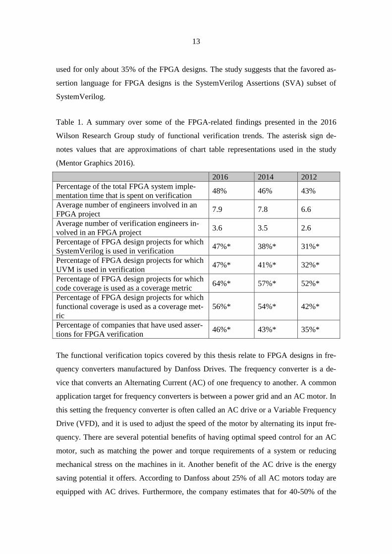
Table 1. A summary over some of the FPGA-related findings presented in the 2016
Wilson Research Group study of functional verification trends. The asterisk sign de-
notes values that are approximations of chart table representations used in the study
(Mentor Graphics 2016).
2016 2014 2012
Percentage of the total FPGA system imple-
mentation time that is spent on verification 48% 46% 43%
Average number of engineers involved in an
FPGA project 7.9 7.8 6.6
Average number of verification engineers in-
volved in an FPGA project 3.6 3.5 2.6
Percentage of FPGA design projects for which
SystemVerilog is used in verification 47%* 38%* 31%*
Percentage of FPGA design projects for which
UVM is used in verification 47%* 41%* 32%*
Percentage of FPGA design projects for which
code coverage is used as a coverage metric 64%* 57%* 52%*
Percentage of FPGA design projects for which
functional coverage is used as a coverage met-
ric
56%* 54%* 42%*
Percentage of companies that have used asser-
tions for FPGA verification 46%* 43%* 35%*
The functional verification topics covered by this thesis relate to FPGA designs in fre-
quency converters manufactured by Danfoss Drives. The frequency converter is a de-
vice that converts an Alternating Current (AC) of one frequency to another. A common
application target for frequency converters is between a power grid and an AC motor. In
this setting the frequency converter is often called an AC drive or a Variable Frequency
Drive (VFD), and it is used to adjust the speed of the motor by alternating its input fre-
quency. There are several potential benefits of having optimal speed control for an AC
motor, such as matching the power and torque requirements of a system or reducing
mechanical stress on the machines in it. Another benefit of the AC drive is the energy
saving potential it offers. According to Danfoss about 25% of all AC motors today are
equipped with AC drives. Furthermore, the company estimates that for 40-50% of the

14
motors not yet equipped with drives there would be a potential for energy savings if AC
drives were installed (Danfoss Drives 2016). The basic operation principle of an AC
drive is to rectify an AC, store it as Direct Current (DC) to a capacitor and then invert it
back to AC with a desired frequency. One of the main tasks of the FPGA in frequency
converters is to generate the Pulse Width Modulation (PWM) signal that is used to in-
vert DC to AC. As the FPGA is a deterministic and parallel device it is suitable for this
task. FPGAs are also used for other time-critical tasks of the drives, such as low latency
communication between various nodes of the device. Valid behavior of the FPGA de-
signs is therefore crucial for the overall performance of the AC drive. Faulty PWM gen-
eration could cause motor failure in AC motors connected to the drive, while logical
bugs in communication logic could lead to distorted data or data being lost.
At this stage of the study, some assumptions of the coming work are made. These as-
sumptions are based on observations that are made in three studies that were chosen as a
reference for the evaluation done in this paper. According to one of the papers, con-
strained randomized tests were able to discover obscure bugs that would have been hard
to find with conventional directed tests. In this study from 2008 a verification team at
the company in question was evaluating the use of SystemVerilog with a CRV method-
ology that can be considered a predecessor to UVM. The verification team was able to
achieve greater automatization of testing and was eventually finding bugs that would
have been challenging to find with their pre-existing test methodology, which was based
on self-checking directed tests. According to the study there were no time penalties dur-
ing the introduction of these new methods, however, it must be stated that the company,
Rockwell Collins, already had a verification team that was doing testing for safety criti-
cal designs. It can therefore be assumed that the verification was already at a reasonably
high level (Keithan, Landoll, Logan & Marriott 2008).
In the second paper, which was written as a company evaluation case study for Nokia
Networks, an introduction of CRV with UVM is presented. In this paper the writer de-
scribes the verification process for a co-processor designed by the company. Although
the verification effort is not described in great detail, the impression is that for a design-
er with no previous knowledge of CRV and UVM there will be a learning process that

15
is time consuming. In the study a team of two engineers were verifying the co-processor
for a time well over one year and the testing was still not complete. However, the DUT
of the study is a system-wide design that can be considered complex. The writer’s esti-
mation is that at the time of writing the study, the time spent in verification is already
greater than 50% of the total time spent on the system implementation (Ihanajärvi
2016).
The third paper referenced for this thesis describes an introduction to UVM for unit test-
ing. The study provides valuable insight into what challenges may be faced by a design-
er that is new to UVM. According to the paper the biggest challenge was the implemen-
tation of verification components that require synchronization between the class-based
test bench and the DUT. Nonetheless, the raised level of abstraction that comes with
UVM was regarded as an advantage, especially for speeding up the creation of test se-
quences by hiding away low-level signal specific details of the test bench. In addition, it
is concluded that after the initial challenges faced in the implementation of the first test
bench, the following test bench implementations are significantly easier and benefit
from the reusability provided by UVM (Francesconi, Rodriguez & Julian 2014).
One of the theorized challenges of creating CRV test benches is the DUT predictor
model implementation. The predictor model, which is the self-checking mechanism of
the CRV test bench, will be discussed further in Chapter 3.1.4. Nevertheless, it is essen-
tially the component of the test bench that automates the checking of response against
the predicted response. Based on the experiences of Francesconi et. al., the theory is that
the creation of a predictor model that is completely synchronized with the DUT and
faultless could for some designs be a challenging task that requires plenty of design ef-
fort. The challenge is not only limited to functional verification of digital designs, as in
fact the digital twin, a digital model of a physical object or system, is a concept that
has gained popularity throughout various fields of technology (Marr, Bernard 2017).
Furthermore, another expectation for the work is that it will be challenging to define
general rules for what is sufficient test coverage for a DUT. The role of functional cov-
erage, which is a term related to Coverage Driven Verification (CDV), should be dis-
cussed in the context of the verification strategy together with code coverage. Although

16
the designs that are tested vary in their purpose, it would be beneficial to have metrics
for what can be considered a sufficient amount of testing.
17
3 VERIFICATION CONCEPTS OF THIS STUDY
3.1 Constrained Random Verification and Coverage Driven Verification
The functional verification methods that are evaluated throughout this thesis are associ-
ated with two fundamental verification concepts – Coverage Driven Verification (CDV)
and Constrained Random Verification (CRV). These two are linked with each other as
they are often applied together. The definitions of these concepts are described in the
following paragraphs.
In CDV the quality measure of the test is coverage. The idea of CDV is to create tests
that cover as much of the DUT’s functionality as possible, which is measured with code
coverage and functional coverage. Code coverage, presented in Chapter 4.3, represents
the implicit properties of the DUT, such as the amount of statements in the code that
have been exercised throughout the simulation. Functional coverage, however, is explic-
itly defined by the designer of the test bench. Functional coverage should be based on
the requirements of the DUT, and it is therefore unique for each verification environ-
ment. Functional coverage for a digital filter could be defined as a set of sine wave fre-
quencies that have to be driven as stimulus to the filter in order to ascertain that the de-
sign was adequately tested. A communication protocol implemented in a digital design,
however, requires functional coverage that is based on its protocol specifications. The
Advanced Extensible Interface, or AXI, for example, has modes for single data word
transmission and burst transmission, and therefore requires functional coverage for dif-
ferent transmission sizes (ARM Holdings 2018). Functional coverage will further be
described in Chapter 5.3.
What is not defined by the CDV ideology, but what a successful implementation of it
requires, is a method of being able to write a large amount of relevant test stimulus.
This is where CRV complements CDV. In CRV the stimulus is randomized within lim-
its that are specified by constraints. Throughout this thesis CRV will be used to refer to
tests that not only utilize constrained randomization, but also fulfill the CDV principles.

18
The AXI-protocol implementation mentioned in the previous paragraph required func-
tional coverage for its transmission sizes. In CRV a constraint could be defined as a
range that corresponds to the length of data transmissions that are written to the DUT.
The constraints are optional and can be specified for each variable in the test bench. In a
CRV verification environment stimulus is randomized prior to each transaction, and if
the stimulus has constraints, the randomization will conform to these. As randomization
automates the stimulus generation, a randomized test bench is also able to drive a great-
er amount of stimulus than a directed test bench, in which the designer has written the
stimulus manually. What a CRV test bench therefore requires is a self-checking mecha-
nism for the response from the DUT. The self-checking component is usually imple-
mented as a comparator that compares the predicted response of the DUT with the actu-
al response received from it. Chapter 3.1.4 describes such implementations in more de-
tail.
3.1.1 The Hardwave Verification Language features of SystemVerilog
A language that has become widely popular for verification of digital designs is Sys-
temVerilog, which is based on the Verilog HDL language, but also includes language
constructs that are intended for verification. In other words, SystemVerilog is not only a
HDL, but also a Hardware Verification Language, or HVL. HVLs include features from
high-level programming languages that are useful for the creation of test benches. As
test benches do not have to be synthesizable, they do not have to be limited to the syn-
tax of HDLs. HVL features are well suited to the CDV and CRV concepts, as functional
coverage, for example, is supported by SystemVerilog through its use of cover-groups,
cover points and cross-coverage. Randomization and constraints are also basic features
of the SystemVerilog verification language. In SystemVerilog the test bench architec-
tures are often associated with the use of Object-Oriented Programming (OOP). In ob-
ject-oriented test benches classes correspond to verification components that all have a
specified purpose. Furthermore, in these test benches bundles of signals representing
interfaces are instantiated and handled as objects. Due to these properties, a test bench
structure is achieved that is not only modular, but also reusable for designs with the
same interfaces. This reusability has the potential of reducing test bench creation time.
19
Additionally, as bundles of signals are treated as objects in the test bench, stimulus can
easily be written for transactions instead of single signals. This is well suited with the
verification concept of Transaction Level Modeling (TLM) that will be described in
Chapter 3.1.2. SystemVerilog also includes another beneficial feature for verification,
which is unrelated to the features mentioned above: the SystemVerilog Assertions
(SVA) subset language.
3.1.2 Transaction Level Modeling
TLM, in the context of verification, builds on the idea that stimulus is written to a bun-
dle of signals concurrently, and that the randomization of these signals can be per-
formed as one operation. The purpose of TLM is to create an abstraction layer that is
above the signal level of the design. Digital designs that are modular, such as those that
are built on IP-cores, often consist of interfaces of coherent signals. In verification of
digital designs, identifying these interfaces of the DUT is a prerequisite for building
transaction level object-oriented test benches, as transactions in these test benches are
instantiated as objects.
Raising the abstraction layer not only makes it easier to simultaneously randomize
stimulus, it also saves time during simulation (Bowyer 2006). In CRV test benches cer-
tain classes are modeled on the transaction level and are therefore not dependent on the
cycle-accurate behavior of the DUT. Consequentially, the procedures of these classes
are event-based and do not have to execute unless the specified event is triggered. Addi-
tionally, making test bench classes dependent on events rather than cycle-accurate be-
havior will arguably make the operations of the said classes easier to comprehend. The
classes modeled on the transaction level naturally require that there is an underlying set
of classes that handle the cycle-accurate behavior of the test bench, but in general, TLM
is not intended to verify cycle-accurate behavior of the DUT. Instead, TLM better suits
the DUT specifications that are written as higher level requirements, not as cycle-
accurate behavior. In other words, the response from the DUT is not assumed to be of
importance on every clock cycle of the simulation. Instead, in TLM test benches events
20
are triggered by specified events of the DUT. The triggered test bench events can be re-
lated to self-checking of DUT response or coverage collection.
TLM requires that the self-checking component of the test bench is modeled on a higher
abstraction layer than the DUT. The self-checker is therefore programmed with HVL
features rather than as HDL code. The DUT functionality determines the level of effort
that goes into modeling an equivalent predictor model of the DUT. For example, if the
DUT implements an algorithm that was originally modeled and tested in a software lan-
guage, the software model can be used as a predictor model in the test bench. In such
cases the stimulus written to the DUT calls a function that updates the predictor model,
which is then compared to the actual response received from the DUT. The predictor
model exported from the original software implementation would therefore be reusable
for the CRV test bench as it is modeled on the transaction level.
3.1.3 The Universal Verification Methodology
UVM is a methodology that implements the concepts presented in the previous sub-
chapters of Chapter 3. The methodology is upheld by Accellera Systems Initiative, a
standards organization, and is therefore not tied to a simulator tool distributed by one
designated vendor. UVM defines a class-based test bench architecture that is intended to
standardize the way that coverage driven constrained random test benches are built. In
addition to defining a set of classes for the test bench architecture, UVM also defines a
set of phases of testing, such as the build phase, the connect phase, the run phase and
the report phase. Out of all UVM phases only the run phase consumes simulation time,
and it is therefore the only phase that implements SystemVerilog tasks. The other UVM
phases might for example build the test bench prior to the test and gather the coverage
report after the test.
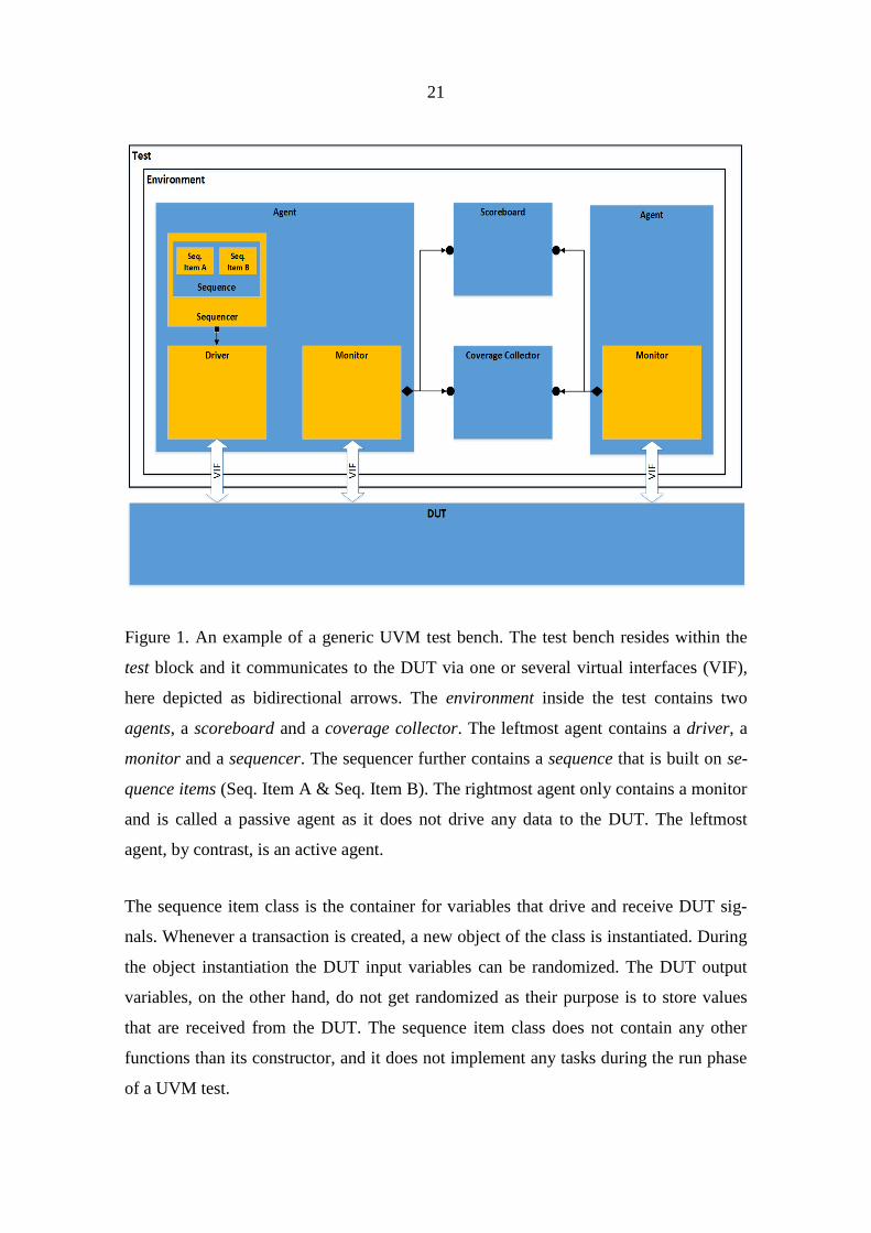
An example of a UVM test bench architecture is depicted in Figure 1. The block dia-
gram contains classes that are generally found in UVM test benches. The exact architec-
ture of a test bench will always depend on the DUT and its interfaces. The following
paragraphs will describe the UVM classes in a bottom-up order.
21
Figure 1. An example of a generic UVM test bench. The test bench resides within the
test block and it communicates to the DUT via one or several virtual interfaces (VIF),
here depicted as bidirectional arrows. The environment inside the test contains two
agents, a scoreboard and a coverage collector. The leftmost agent contains a driver, a
monitor and a sequencer. The sequencer further contains a sequence that is built on se-
quence items (Seq. Item A & Seq. Item B). The rightmost agent only contains a monitor
and is called a passive agent as it does not drive any data to the DUT. The leftmost
agent, by contrast, is an active agent.
The sequence item class is the container for variables that drive and receive DUT sig-
nals. Whenever a transaction is created, a new object of the class is instantiated. During
the object instantiation the DUT input variables can be randomized. The DUT output
variables, on the other hand, do not get randomized as their purpose is to store values
that are received from the DUT. The sequence item class does not contain any other
functions than its constructor, and it does not implement any tasks during the run phase
of a UVM test.

22
The sequence class is used to model sequences that consist of sequence items. For ex-
ample, if a communication protocol implements a burst mode for data transmission, the
sequence item could represent a data word and the sequence the complete data frame. A
UVM sequence is usually parametrized with the type of sequence item it consists of. A
sequence can only be built of objects of the parametrized sequence item class and ob-
jects of its extended classes. However, it is also possible that a sequence is built on oth-
er sequences. Such sequences are called nested sequences.
The sequencer is the container for sequences and sequence items. The sequencer is the
class that is called when generation of sequences is desired, and it contains functions for
transmitting the sequences towards the DUT. This class usually does not require actions
by the designer of the test bench as its functions are provided by the UVM package.
The driver class receives sequences from the sequencer and drives them to the DUT.
The driver converts the received sequences, one sequence item at a time, into signal lev-
el assignments that are driven to the DUT, after which it gives back control to the se-
quencer. The driver only drives signals to the DUT and does not monitor received re-
sponse. An exception to this is handshake communication that requires that a response
event from the DUT activates before subsequent signals can be driven to the DUT. Be-
cause the driver operates on the signal level it is a part of the UVM test bench environ-
ment that is cycle-accurate. The driver therefore contains a task with clock-
synchronized logic. The logic of the driver depends on the functionality of the DUT in-
terface that it communicates with.
The monitor class is a component of the UVM test bench that monitors communication
to and from the DUT. The monitor also operates on the signal level, however, it usually
only triggers on certain events. A triggering event activates assignments that write data
to a monitoring stream. The assignments write signal values from the virtual interface to
variables of the test bench. In UVM the monitoring stream that is connected to a moni-
tor is known as an analysis port. The analysis port is connected to classes in the test
bench that handle monitored data. The receiving end of an analysis port is called an

23
analysis export. A monitor never drives data to the DUT and it can contain multiple
analysis ports that are triggered by separate events.
The classes mentioned so far are all contained in an agent class. In UVM the agent is
intended to be a reusable verification component and therefore it is recommended that
the classes inside it are designed in a generic manner that allows for reuse. The agent is
only a container class and its only purpose is to build the components inside it and route
analysis ports to its outer boundary. An agent can be either active or passive. An active
agent contains a driver and a sequencer while a passive agent does not. The latter can be
used for example if an internal signal of the DUT is monitored with a SystemVerilog
bind statement and used for coverage collection. Figure 1 contains an active and a pas-
sive agent.
The class that encapsulates UVM agents is called the environment. The role of the envi-
ronment, similarly to the agent, is to build classes inside itself but also to connect analy-
sis ports from outer boundaries of agents to analysis exports of other classes contained
within itself. Classes that are not suitable for reuse are generally placed in the environ-
ment instead of being placed inside the agents. In the block diagram of Figure 1 two
such classes are present in the environment.
The scoreboard class implements the self-checking of the test. It compares the response
of a predictor model with the actual response of the DUT. The predictor model is an
equivalent of the DUT that is generally modeled on a higher level of abstraction than
the real design. It can be considered as the golden reference for the design that conforms
to the design specifications. The predictor model can either be implemented inside the
scoreboard or it can be an independent class outside of it. In Figure 1 it is assumed that
the predictor model has been implemented internally. The scoreboard can be connected
to multiple agents, as can be seen in Figure 1, and it has several methods for handling
monitoring events. The functionality of a UVM scoreboard will be described in more
detail in Chapter 3.1.4.
24
In addition to the scoreboard, the environment depicted in Figure 1 also contains a cov-
erage collector. While UVM does not actually define a coverage collector class, it has
been named so in Figure 1 for clarity. The UVM cookbook by Mentor Graphics pre-
sents two UVM classes that are suitable for coverage collection: the subscriber class
and the component class (Mentor Graphics 2012). The subscriber class extends the
component class and offers a simplified method for writing monitored data from one
monitor to the coverage collector. The subscriber implements a write-function that is
automatically called whenever monitored data is received. However, the subscriber is
restricted to only one monitoring stream. For coverage collectors that require multiple
monitoring streams the UVM cookbook recommends the use of the component class.
The coverage collector is the class that contains the SystemVerilog covergroup, cover-
point and cross-coverage statements that gather functional coverage during a test.
Whenever a transaction is received from a monitoring stream the functional coverage is
updated.
The final class to be presented in this chapter is the test class. The test class is a contain-
er for the environment class, which it builds prior to the run phase of a test. Once the
simulation proceeds to the run phase, sequencers contained within the agents of the en-
vironment are called from the test class. In UVM test completion is controlled with ob-
jections. Generally, an objection is raised before the sequencers are started in the test
class, and dropped once all sequencers have finished their stimulus generation. A
dropped objection signals the UVM test bench to proceed from the run phase to its fol-
lowing phases, at which point test reports are gathered and written to files.
3.1.4 Self-checking test benches
A successful UVM test requires a self-checking component that automates the task of
checking the validity of the DUT response. When building the test bench the self-
checking activities of it are arguably the most challenging to design. For the implemen-
tation of the predictor model there are not many common guidelines, as the DUT im-
plementations are all unique. What can however be generalized are the methods of how
to store the predicted responses, when to trigger a scoreboard comparison and how to do

25
it. All of these depend on the nature of the transaction stream from the DUT. When de-
signing a self-checking test bench it is important to identify the conditions for when a
scoreboard comparison should be made. In this chapter three useful methods for differ-
ent types of DUTs are presented in Figures 3-5. In the figures the predictor models are
not shown and are assumed to be separate from the scoreboards. However, the predic-
tors can also be implemented internally into the scoreboard, in which case the predicted
response in the figures would arrive from an internal predictor.
Figure 3. An In Order Scoreboard. A transaction that is written to the DUT results in a
predicted response, which is stored in an Analysis FIFO in the scoreboard. Once the ac-
tual response of the DUT is received, it triggers a comparison with the predicted re-
sponse. The predicted response is popped from the Analysis FIFO upon being triggered
by the actual response.
Figure 3 depicts an In Order Scoreboard for which the order of stimulus and response is
known. In its simplest form the scoreboard contains one Analysis FIFO for the predict-
ed response. In this model the Compare-function is called once the response is re-
ceived from the DUT. If multiple transactions have been stored in the FIFO, the one that
was stored first in the buffer is popped. An example use case for the In Order Score-
board could be an Arithmetic Logic Unit (ALU) that calculates the sum of two numbers.
26
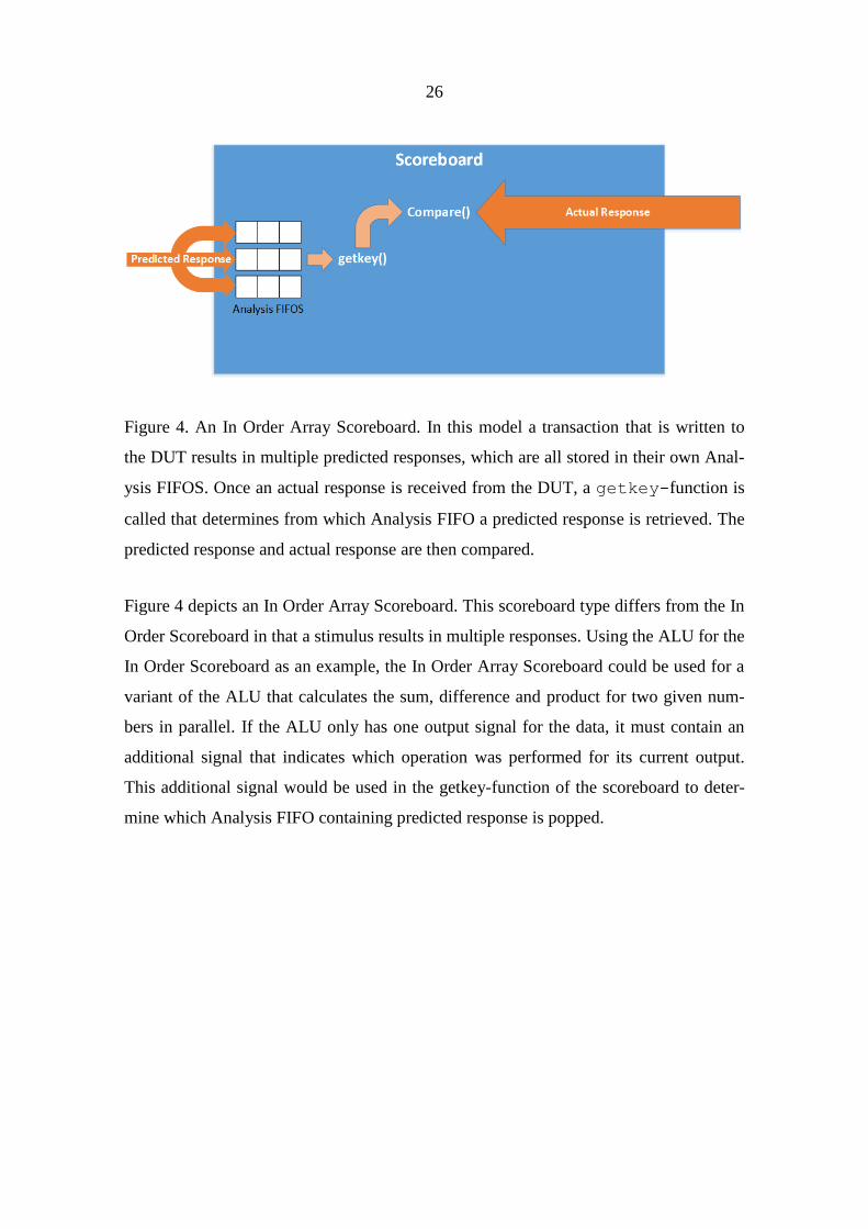
Figure 4. An In Order Array Scoreboard. In this model a transaction that is written to
the DUT results in multiple predicted responses, which are all stored in their own Anal-
ysis FIFOS. Once an actual response is received from the DUT, a getkey-function is
called that determines from which Analysis FIFO a predicted response is retrieved. The
predicted response and actual response are then compared.
Figure 4 depicts an In Order Array Scoreboard. This scoreboard type differs from the In
Order Scoreboard in that a stimulus results in multiple responses. Using the ALU for the
In Order Scoreboard as an example, the In Order Array Scoreboard could be used for a
variant of the ALU that calculates the sum, difference and product for two given num-
bers in parallel. If the ALU only has one output signal for the data, it must contain an
additional signal that indicates which operation was performed for its current output.
This additional signal would be used in the getkey-function of the scoreboard to deter-
mine which Analysis FIFO containing predicted response is popped.
27
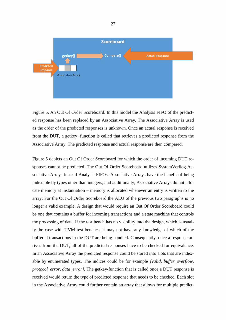
Figure 5. An Out Of Order Scoreboard. In this model the Analysis FIFO of the predict-
ed response has been replaced by an Associative Array. The Associative Array is used
as the order of the predicted responses is unknown. Once an actual response is received
from the DUT, a getkey-function is called that retrieves a predicted response from the
Associative Array. The predicted response and actual response are then compared.
Figure 5 depicts an Out Of Order Scoreboard for which the order of incoming DUT re-
sponses cannot be predicted. The Out Of Order Scoreboard utilizes SystemVerilog As-
sociative Arrays instead Analysis FIFOs. Associative Arrays have the benefit of being
indexable by types other than integers, and additionally, Associative Arrays do not allo-
cate memory at instantiation – memory is allocated whenever an entry is written to the
array. For the Out Of Order Scoreboard the ALU of the previous two paragraphs is no
longer a valid example. A design that would require an Out Of Order Scoreboard could
be one that contains a buffer for incoming transactions and a state machine that controls
the processing of data. If the test bench has no visibility into the design, which is usual-
ly the case with UVM test benches, it may not have any knowledge of which of the
buffered transactions in the DUT are being handled. Consequently, once a response ar-
rives from the DUT, all of the predicted responses have to be checked for equivalence.
In an Associative Array the predicted response could be stored into slots that are index-
able by enumerated types. The indices could be for example {valid, buffer_overflow,
protocol_error, data_error}. The getkey-function that is called once a DUT response is
received would return the type of predicted response that needs to be checked. Each slot
in the Associative Array could further contain an array that allows for multiple predict-

28
ed responses to be active for each enumerated type. If a valid output would be received
from the DUT, all predicted responses inside the valid slot of the Associative Array
would be checked. If no valid entries exist in the Associative Array, an error would be
raised.
3.2 Temporal Logic verification
In addition to verification on the transaction level, verification can also be performed at
a lower level of the design with temporal logic statements. Temporal logic verification
is the validation of a design’s behavior in terms of time, which in digital designs most
often is related to a clock. The following two statements are examples of temporal logic.
“I am tired until I rest” and “If I don’t eat I will eventually get hungry”. The words “un-
til” and “eventually” are modal operators that specify a relation in time between the first
part of the statement and the second part of the statement. A digital design can similarly
be described by statements that should always, eventually or never hold true. Further-
more, statements can be combined to form layers of temporal logic, for which the valid-
ity can be checked with assertions. In this thesis verification for temporal logic will not
be evaluated, however, as research shows that assertions have become increasingly
common in digital design verification, it was decided that an introduction to this topic
would be provided. Assertions have been used in conjunction with CRV testing to en-
hance the quality of testing, and therefore assertions will be discussed in Chapter 8 in
the context of potential future research. Two publications are used for reference
In verification of digital designs or software temporal logic is regarded as a type of for-
mal verification. Common languages used for temporal logic verification of digital de-
sign are the Property Specification Language (PSL) and the SystemVerilog subset lan-
guage SystemVerilog Assertions (SVA). The languages are similar in that they both de-
fine a layered structure for modeling a design behavior, often illustrated as a pyramid.
An illustration will be given in Figure 6. In both languages the bottommost layer is a
Boolean layer that defines statements such as A and B. Boolean statement by adding a
time relation to it and making an assertion of the resulting temporal statement. In Chap-

29
ter 3.2.1, an SVA assertion is demonstrated. In this thesis two publications are used as
reference on Assertion Based Verification (ABV)(Foster, Krolnik 2008)(Foster,
Krolnik, Lacey 2010).
3.2.1 SystemVerilog Assertions
SVA is an assertion language that has gained popularity in digital design verification. It
separates assertions into two types: immediate assertions and concurrent assertions.
Of these two types the former is a non-temporal assertion while the latter is temporal.
Immediate assertions can only be placed within procedural statements, such as always-
blocks in SystemVerilog, and they evaluate in zero-time. Concurrent assertions, in con-
trast, are evaluated over several clock cycles and can be triggered by a certain condition.
Out of these two types of assertions, the concurrent assertions are of greater interest for
in this study. Assertions, whenever referenced from now on in this study, are therefore
assumed to be of the concurrent type.
As described in Chapter 3.2, SVA defines a layered structure for building assertions for
temporal statements. The structure is depicted in Figure 6 below.

30
Figure 6. An illustration of the temporal layers of SystemVerilog concurrent assertions.
The bottommost layer defines boolean expressions without time relations. The layer
above expands the boolean expressions by creating event sequences of them. The event
sequences are specified in terms of clock cycles. Sequences are further used by proper-
ties on a layer above. Properties can also be built on properties consisting of sequences.
On the topmost layer assertions are made of properties.
The following paragraphs will give an example of an assertion that is built by the multi-
layered approach. The example describes a handshake protocol with a request and
acknowledge signal. The concurrent assertion is based on the timing diagram of Figure
7.

31
Figure 7. A timing diagram of a handshake protocol. When the request signal req ris-
es, the acknowledge signal ack must rise after two clock cycles.
The Boolean expression of this concurrent assertion is not actually necessary, but it will
be defined explicitly in this example. The Boolean expression is described by the fol-
lowing line of code.
req == 1
The Boolean expression can also be simply expressed as req. The following lines of
code describe the sequence that is built on top of the Boolean expression. The sequence
states that the ack signal must be asserted two clock cycles after req is asserted.
sequence req_ack_seq;
req ##2 ack;
endsequence
The layer above the sequence layer makes a property of the above sequence. The result-
ing property is described by the following code segment.
property handshake;
@(posedge clk) req_ack_seq;
endproperty
The property defined above evaluates the sequence that was modeled on the positive
edge of the clock. Below is the code segment that makes an assertion of this property.
handshake_assertion: assert property(handshake)
else $error(“Handshake error”);
32
A concurrent assertion and its underlying temporal statements can either be defined in
an interface or a module.
3.2.2 Assertions used as protocol checkers
Assertions are valuable in verification whenever design behavior can be described in
detail on a cycle-accurate level. The use of assertions therefore requires a knowledge of
the design often only possessed by the designer of the DUT. Design documentation of
an IP rarely describes the design in detail with timing diagrams that can be used to
model assertions. However, interfaces are usually well understood as documents gener-
ally contain their timing information. Consequently, assertions can be modeled for these
with a relatively small effort and be used as checkers that monitor interaction between
the modules of an individual IP-block or the interaction between IP-blocks in a system
level design. These checkers increase the visibility into the DUT and may be beneficial
for discovering the root cause of a bug. In a test bench without assertions the debugging
process arguably requires more effort as the problem cause must first be established be-
fore the design can be fixed.
3.2.3 Using assertions to complement test benches
Assertions can be used to complement CRV test benches, but if assertions are used in
conjunction with a UVM test bench, they must be defined outside of the UVM classes.
An assertion IP can be made of a module, or alternatively the assertions can be placed
inside a SystemVerilog interface. While the UVM scoreboard checks the response of
the DUT on the transaction level, the assertions can check cycle-accurate behavior. The
assertions can be of additional value as they can be used to off-load some of the check-
ing that would otherwise have to be implemented in the predictor model. Assertions
could also be made during the design phase of the DUT by the designer that has
knowledge of the IP.
Assertion IPs can also be used together with test benches created in Verilog or VHDL if
a simulator tool is used that supports concurrent assertions. Verilog and VHDL do not

33
have concurrent assertions and are therefore limited to assertions in procedural blocks.
Presumably many companies already have an existing system level test bench that is
implemented in one of the two aforementioned languages. In such case assertion IPs can
be added to the testing without any modifications to the existing test bench. The asser-
tion IPs can be instantiated as additional test bench modules that are simulated in paral-
lel with the top-level module of the system level test bench.
34
4 PRESENT TESTING METHODS OF THE COMPANY
4.1 Simulation-based test types in use
At Danfoss Drives the FPGA design team implements three types of simulated tests: the
IP-block level test, the system level test and the release test. Out of these three tests only
the first two will be covered with case studies in this paper. The release test, which will
be excluded from this thesis, is a test that is applied to a system level design before it is
handed over to the software team. At present, the purpose of this test is not to extensive-
ly test the behavior of the design, but to perform directed tests at features that are known
to cause problems in the integration phase of the firmware on the embedded processor
and the FPGA. An example of such a feature is the polarity of the reset-signal. Howev-
er, the actual test coverage of the FPGA designs is gathered by the IP-block level test
and the system level test. The latter validates the behavior of a system level design that
contains multiple IP-blocks. Before an IP-block is tested in the system level test it is as-
sumed that it has already been tested with an IP-block level test bench. The system-level
test will also be referred to as the integration test throughout this thesis.
The lowest level of testing is performed at the IP-block level. The IP-block can consist
of one or several modules, but it’s the smallest unit of reusable logic in an integrated
digital design. In the context of testing, the IP-block is easier to test than an integrated
system. Apart from containing less logic and having better interface access into the de-
sign, the IP-block usually implements a function that is clearly defined. It is also in gen-
eral easier to gather extensive coverage for an IP-block than during a later phase in the
system level test, as the simulation time of an IP is likely to be less than for a larger de-
sign. It is customary that the designer of the IP-block, or one of its designers, writes the
design specification for the IP-block in question. As the IP-block level test is considered
a part of the design process, it is usually implemented by one of the designers responsi-
ble for the Register Transfer Level (RTL) logic of the IP.

35
4.2 Verification methods in use
The tests described in Chapter 4.1 are written in the VHDL language and are mostly
performed as test cases with predefined stimulus for which results are validated with
VHDL assertions. Procedures and functions are used to generate reusable code for re-
curring tasks such as generic write and read tasks for certain interfaces. For such inter-
faces the level of abstraction can be considered to have been raised to the transaction
level. Randomization with VHDL has been used for some tests, but in general the cur-
rent testing methodology can be reviewed as directed testing (Bartley, Galpin & Black-
more 2002). In directed testing the DUT is driven to states with known responses. The
behavior for the intended functions of the DUT are known by the designer and should
also be documented in the design specification. With directed tests so called corner cas-
es of the design’s behavior are generally targeted with dedicated test cases. Corner cases
of a design can usually be predicted as they are cases for which bugs are likely to be
found. An example of a corner case is the overflow condition for a buffer. As the se-
quence of events is known in directed testing, and the amount of driven stimulus is gen-
erally less than for a random stimulus test bench, debugging also requires less effort
than for a randomized test. If extensive coverage of the design is desired, however, the
amount of test cases will increase and cause an overhead in the effort required for de-
signing and maintaining the test bench. Directed testing is also potentially hazardous as
bugs may remain uncovered for obscure DUT behaviors.
The test benches of the FPGA design team usually consist of a series of test cases that
target some functionality of the design. The amount of test cases depends on the com-
plexity of the design. The system level test bench, which has been expanded over time
as more features have been designed, currently consists of approximately 30 test cases.
For reporting test results, code coverage, which will be described in Chapter 4.3, has
been introduced as a metric of testing quality. Code coverage is not intended to indicate
whether certain design requirements have been validated through testing or not, it is
merely used as an approximation of how much of the RTL code of the design has been
covered by the test. The coverage in terms of functionality is currently not reported.

36
4.3 Test reporting with code coverage
The test results are reported for each IP-block as a percentage of achieved code cover-
age. The code coverage of an IP-block is the combined sum of the coverage gained from
the IP-block test and the system level test, which the simulator tool is able to merge.
The tool does not raise the total coverage if there are overlaps in covered features, and
for example, a statement that is executed in multiple tests is only added once to the total
statement coverage. Code coverage is a concept that defines a set of metrics that are
measured during a simulation of software, or in this case RTL code. The code coverage
that is measured by the FPGA design team at Danfoss Drives is presented in the follow-
ing paragraphs. As there are variations between the definitions provided by the vendors
of the simulator tools, it is worth to notice that the definitions presented here are derived
from the Questasim User Manual written by Mentor Graphics (Mentor Graphics 2015:
815-843). The Questasim simulator is the simulator tool that is used during the evalua-
tion of the CRV tests presented this thesis.
Statement coverage counts the execution of statements in the source code. Statement
coverage resembles line coverage, with the difference that a line in the source code can
consist of several statements. The Mentor Graphics simulators Modelsim and Questasim
do not measure line coverage, only statement coverage.
Branch coverage counts the execution of branches in if/else and case branch
statements. An if-statement with multiple nested else if-statements and an else-
statement must have all of its branches executed at least once in order to have been fully
covered by branch coverage.
Toggle coverage, in standard mode, regards signals in HDL source code as bit vectors
and counts the amount of times each bit has been toggled from 0 to 1 and from 1 to 0.
There is also an extended mode of toggle coverage for tri-state signals. These signals
have an additional state – the high impedance state Z. The extended mode counts all
variations of toggles between 0, 1 and Z. The toggle coverage that is used by default by
the FPGA design team at Danfoss Drives is the standard mode.

37
Finite State Machine coverage counts the amount of times each state and state transi-
tion of a Finite State Machine (FSM) has been executed. FSM coverage is useful in
RTL design verification as it might reveal logical bugs related to FSMs. Common FSM
related bugs include states that are unreachable and state transitions that cannot occur.
Condition coverage counts the execution of each variation of a subexpression in a con-
dition statement, such as an if-statement. For example, the following if-statement
written in VHDL contains a subexpression, where signals A and B are one-bit wide sig-
nals.
if(A and B)then
C <= C+1;
end
The subexpression A and B contains two bits and therefore has four unique input en-
tries. A condition coverage of 100 % would require that all of these have been covered
during the simulation. However, an increased amount of input bits leads to an exponen-
tial increase in the amount of unique input entries. Standard condition coverage is there-
fore not an option for subexpressions consisting of bit vectors. As a solution, several
vendors offer Focused Expression Coverage (FEC) as its default condition coverage.
This is also the case with Modelsim and Questasim, the tools used at Danfoss Drives.
The following definition of FEC is cited from the Questasim User Manual.
In FEC, an input is considered covered only when other inputs are in a state that
allow it to control the output of the expression. Further, the output must be seen
in both 0 and 1 states while the target input is controlling it. If these conditions
occur, the input is said to be fully covered. The final FEC coverage number is
the number of fully covered inputs divided by the total number of inputs (Men-
tor Graphics 2015).
If a conditional statement contains an expression that consists of several subexpressions,
FEC makes a simplification of the full expression before it evaluates each input. For

38
example, in order to evaluate the FEC condition coverage of input A in the following
VHDL if-statement, the expression is first simplified.
if(A and B and C and D)then
The simplified statement of the above if-statement is
if(A and Expression_1)then
The logic expression B and C and D has now been reduced to Expression_1. In
order to fully cover input A, Expression_1 must be true. When the expression is
true, A has exclusive control over the output. Input B is according to the principle of
FEC only evaluated when A is true, as the evaluation of the conditional statement
moves from left to right. The FEC condition coverage for B is therefore evaluated with
the following simplified statement, assuming that A is true.
if(B and Expression_2)then
In the above statement Expression_2 corresponds to C and D of the original ex-
pression.
Expression coverage is the last of the coverage metrics generated by Questasim and
Modelsim that is used by the FPGA design team. Expression coverage is similar to con-
dition coverage, except that the statement is a Right Hand Side (RHS) statement of a
signal assignment, such as in the following example written in VHDL.
A <= B or C and D;
The same problem occurs with expression coverage as with condition coverage. The
state space for the input entries can be too vast to cover if the inputs are bit vectors. Ex-
pression coverage is therefore by default also gathered as FEC in Modelsim and Ques-
tasim.
39
5 VERIFICATION STRATEGY
In this chapter verification strategies for the IP-block test and the integration test will be
presented. The presented strategies are intended as guides for creating tests that are
based on the functional verification methodologies presented in this thesis. The strategy
defines what kind of tests are performed for either the IP-block or the integrated system,
what the objective of each test is, how self-checking is implemented and whether ran-
domization and functional coverage is used. Three strategies are introduced in total –
two for the IP-block test and one for the integration test. The presented strategies as-
sume a bottom-up order of verification, in which an IP-block is tested before the inte-
gration test is performed.
5.1 Verification strategies for the IP-block test
The proposed strategies for IP-block testing are based on a black-box approach and are
implemented as CRV test benches, UVM being the methodology of choice. In black-
box testing it is assumed that the internal functionality of the DUT is non-visible. There-
fore, the verification is performed on a higher level of abstraction that only validates the
behavior of the DUT through its peripheral signals. White-box verification, on the other
hand, assumes that the internal functionality of a design is visible. In white-box verifica-
tion the behavior of the DUT is validated on a lower level of abstraction within the
DUT and on its periphery.
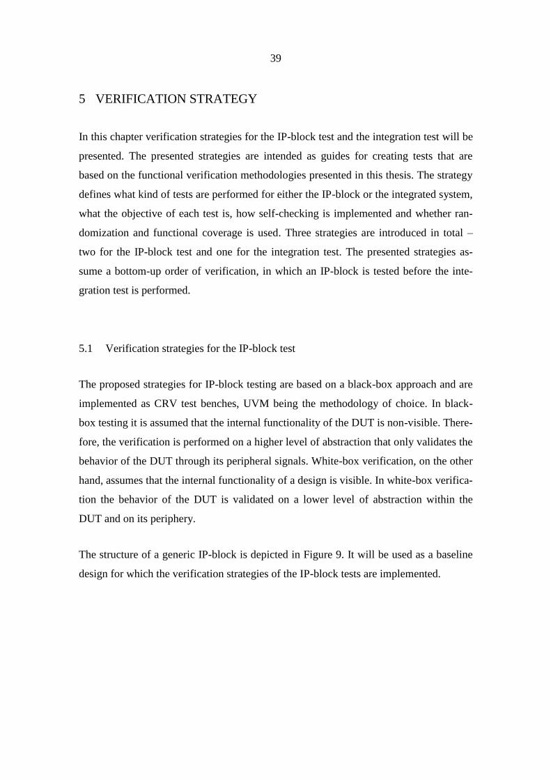
The structure of a generic IP-block is depicted in Figure 9. It will be used as a baseline
design for which the verification strategies of the IP-block tests are implemented.
40
Figure 9. An example of a generic IP-block that contains a submodule for user registers
and a submodule for user logic. The peripheral interface, if one exists, usually interacts
with the user registers of the IP. The user logic acquires configurations from the user
registers through internal signals of the IP. Input and output signals not part of a periph-
eral interface may also be mapped from the top module directly to the user registers or
the user logic.
5.1.1 Full IP test bench
In the first proposed strategy the full IP-block will be regarded as the smallest unit that
is tested. In designs that interact with software of an embedded processor, IP-blocks can
be accessed through a peripheral interface that is usually based on a protocol such as
AXI. A commonly used practice is to configure the IP-block from the software with
write operations to the user registers of the design. Additionally, if the IP is a co-
processing block that is used in conjunction with processes in the software, registers of
the IP-block are read by the software, usually by polling the status registers of the IP.
The input and output signals of the DUT that are not a part of its peripheral interface are

41
routed to other IP-blocks in a system-wide design and are therefore not necessarily ac-
cessible by the software. The full IP test bench implements a predictor model for the
user logic of the IP that also contains a register model for the user registers in the IP.
In Chapter 3.1.4 fundamental self-checking mechanisms of CRV methodologies were
introduced. Common for all self-checkers is that there must be a condition that signals
the start of an event and another condition to signal a finalized event. The latter will
here be referred to as the stop condition. For an IP-block such as the one depicted in
Figure 9, the start and stop conditions can be obscure as they are marked by signals that
are hidden inside the DUT. A challenge that was encountered at the start of the thesis
work was indeed related to these signals. A full IP test bench sends a transaction to a
user register that signifies the start of an event. However, the actual start condition can
be received by the user logic of the DUT after a delay of a few clock cycles. As the pre-
dictor model of the test bench must be synchronized with the DUT in order to be valid,
the delay before the event is registered by the predictor model must be equivalent to the
delay inside the DUT. This will inevitably mean that the designer of the test bench must
have timing specific knowledge of internal logic of the DUT. What can potentially pre-
sent an even greater challenge for the verification engineer, however, is the stop condi-
tion. In designs with a similar design hierarchy as the one depicted in Figure 9, the test
bench must poll a status register of the IP that contains a bit that marks a finalized
event. Furthermore, if the bit is asserted and the event was finalized, the design might
require that one or several user registers containing data are read before the test bench
prediction and actual response can be compared. If the test bench stimulates the DUT
with a known sequence of transactions, the comparison of the prediction and the re-
sponse can be triggered from a predetermined read operation that reads the last data
item that is required for a comparison. However, if the test bench stimulates the design
with a randomized sequence of transactions, the test bench must implement a checking
mechanism that assures that a start condition has preceded a stop condition, and that af-
ter the stop condition has occured, all registers containing response data must be read
before the comparison is performed in the test bench. Consecutively, the complexity of
the predictor model in the test bench increases, and with it the time required to design
the test bench.

42
As the write and read operations to the user registers control the behavior of an IP such
as the one depicted in Figure 9, limitations can be made for what stimulus would realis-
tically be written to the design. It is therefore proposed that the sequences of the full IP
test bench are not fully randomized but split into dedicated test cases. Data can still be
randomized as well as the occurrence of certain stimulating events, but the sequencers
of the test bench will be more constrained. For example, randomized toggling of the re-
set signal can be left out of most tests cases. Also, randomized write operations to user
registers of the design can be implemented in one dedicated test. Table 1 describes test
cases that are generic and that could be implemented instead of one fully randomized
test.
Table 1. Examples of generic test cases that can be implemented by the proposed full IP
test bench.
Test type Purpose of the test
User register write/read test Verify that the write and read rights to the
user registers of the IP conform to the de-
sign specifications
Reset test Verify the behavior of the DUT after a re-
set condition occurs. The reset can occur
at a random time during an active event.
Reconfiguration test Verify the behavior of the DUT after user
register configurations are changed during
an active event.
Data error test Verify the behavior of the DUT when an
input is received that contains erroneous
data.
Protocol error test Verify the behavior of the DUT when an
erroneous message is sent to a communi-
cation bus of the DUT.
Buffer overflow test Verify that the DUT can handle buffer
overflows that are caused by peripheral
communication.
Base test Verify the behavior of the DUT under
normal conditions, if such conditions can
be specified. For a co-processing IP that
communicates with software the transac-
tion sequence might follow a predeter-
mined order.

43
5.1.2 Divide and conquer test bench
Another testing approach that is proposed as an alternative for the full IP test bench is
the divide and conquer method. In this method there are three separate test benches: one
for the user registers of the IP, another for the user logic of the IP and a third for the full
IP. The idea is that the DUT can be tested more extensively with the user register and
user logic test benches, and that the final full IP test bench only implements trivial test
cases that validate correct mapping of signals within the IP. The stimulus written in the
final full IP tests could be predetermined, therefore not requiring a register model and
predictor model. Although the divide and conquer method requires several test benches,
it assumedly requires less effort for creating the predictor model. It is also theorized in
this thesis that it will achieve higher coverage of the DUT than the full IP test bench.
This is due to the fact that the fully randomized test should be able to explore a greater
amount of the state space than tests that are constrained to predetermined event se-
quences.
The user logic test bench is where most of the design will be covered. In the previous
chapter the visibility challenges of the full IP test bench were presented. Because the
user logic module has input and output ports that are mapped to the user registers of the
IP, one of them being the signal that marks a finalized event, it is proposed that the user
logic test bench should stimulate the DUT with a randomized sequence of transactions.
This type of randomization can drive the DUT into a state that uncovers unpredictable
logical bugs. The user logic test bench simplifies the comparison between the predicted
response and the DUT response – the comparison can be made as soon as the stop con-
dition is seen by the test bench. Additionally, the behavior of the DUT after a reset con-
dition is easier to validate as the responses are visible in the output ports of the DUT. In
the full IP test bench the user registers would have to be read one by one after a reset
has occurred.
The divide and conquer method also includes a user register test bench. This test bench
contains a register model that is based on design specifications. The purpose of the reg-
ister model is to validate write- and read-rights to the registers. The register model can

44
also contain registers that are self-clearing or read-only. In this test bench fully random-
ized write or read operations are driven to the DUT, and the comparison can occur ei-
ther when a read operation has been performed or after a fixed amount of clock cycles
has passed since a write operation. If the aforementioned comparison scheme is chosen,
the comparison is only made for the register that was read. If the latter is chosen, the
whole register model is compared to the output ports of the user register module. This
comparison scheme requires that all user registers are mapped to output ports in the user
register module.
After having tested the user logic and user registers separately, the divide and conquer
method still requires a test bench for the full IP-block with a few directed test cases. The
purpose of the tests in this phase is not to raise coverages, only to validate that signals
from the user logic and user registers are mapped correctly and accessible by the top
module. Once these tests have been completed the coverages of all tests in the three test
benches can be merged.
5.2 Verification strategy for the integration test
The verification strategy that is proposed for the integration test relies on capabilities of
the SystemVerilog language that are lacking in a reference integration test bench of the
Danfoss FPGA team. The existing integration test bench is modeled entirely in VHDL
and therefore lacks features that are available in HVLs such as SystemVerilog. HVLs
often include features from high-level programming languages that are practical for in-
stance when modeling the high-level abstraction equivalent of the DUT in the test
bench. Such features are generally not synthesizable in hardware but are functional in
simulation.
A review was made of the existing test bench in order to establish what improvements
could be made in system level testing. However, before these items are listed, it is im-
portant to specify the objectives of testing at this layer. As has been previously stated in
this thesis, the testing follows a bottom-up order where IPs are extensively tested before

45
integration tests are performed. The main priorities of the integration tests are therefore
to ensure that added features work as intended in the system wide design and that no
existing features were broken. As such, there is no need to design tests on this layer that
extensively gather coverage. Because of this limitation it was decided that the case
study of Chapter 5.2 would be implemented without using functional coverage. An add-
ed reason for this decision was that functional coverage would require a license for an
advanced simulator with an expensive license. The deficiencies that were identified with
the existing VHDL test bench are listed in the following paragraphs.
The first observation is the structure of the test bench. Each time a new feature is intro-
duced to the SUT at least one new test case needs to be introduced to the system level
test bench. Understandably the test bench will continue to grow, and consequentially
maintenance of the test bench will become more time-consuming. Modularizing the test
bench will not decrease the amount of code, but it will increase its readability. Sys-
temVerilog supports classes and OOP and can therefore offer a better solution for mod-
ularization than VHDL. The objective of the modularization is to split source code into
files that represent a similar class-based architecture than the one presented in Figure 1.
In VHDL classes and OOP are not supported. The goal of the modularization is to sim-
plify the continuous maintenance of the system level test bench, and to increase the
readability of the code.
The second observation is the stimulus process. In the existing test bench stimulus is
written sequentially. This is a problem for functionalities that require parallel stimulus.
If, for example, an IP performs priority-based arbitration for multiple data channels, but
transactions can only be sent to one channel at a time, the functionality of the IP will
remain untested. Multiple processes can of course be modeled in VHDL, and in this
case, each of these processes would call a procedure that writes to a specified channel.
However, what is argued here is that when there is a significant amount of DUT func-
tionalities that require parallel stimulus, the implementation of a test bench with a class-
based architecture is easier to synchronize and maintain. In a class based SystemVerilog
test bench, for example, an object is first created for a test class, which in turn creates
objects that start the stimulus writing activities for multiple interfaces. A designer not

46
familiar to the test bench, but familiar to a generic class-based test bench architecture,
should be able to identify the functionality of the test bench by inspecting the test class.
The third observation is the monitoring and self-checking of response. As already men-
tioned in the first paragraph of this chapter, SystemVerilog offers high-level program-
ming features that are practical for modeling the predictor of the DUT. Additionally, if
the DUT behavior requires clock cycle accurate checking, SystemVerilog offers concur-
rent assertions. In VHDL assertions are all immediate.
The fourth and final observation is that the integration test lacks the communication be-
tween the processor and the FPGA. In the existing test bench the processors have been
excluded as they are either not portable to the simulators, or there are no methods for
writing stimulus from them or receiving it. In the context of testing, the most important
part of the processor is the AXI bus. To include the AXI communication in the simula-
tion, Bus Functional Models (BFM) are available that simulate the communication be-
tween the processor and the FPGA. The BFMs will also be referred to as Verification
Intellectual Property (VIP) throughout the following chapters. The BFMs act similarly
to agents in any SystemVerilog or UVM test bench and can be used either to initiate
communication, in master mode, or to react on communication, in slave mode. As Sys-
temVerilog is a hardware verification industry trend, BFMs are also well available for
the language. The ability to spawn multiple threads in SystemVerilog is also a function-
ality that is well suited to the use of BFMs.
The inclusion of AXI BFMs is also an interesting aspect as it covers an area of testing
that has previously been left out of the integration test. In Chapter 4.1 the release test
was briefly mentioned, and although it was not chosen as a topic for this thesis, it might
perhaps be possible to combine the two separate tests into one. For the FPGA team it
would mean that testing would only have to be performed in two phases instead of
three.
47
5.3 Functional coverage
Of the three proposed verification strategies, only the IP level tests would utilize func-
tional coverage. However, as it is proposed that the full IP test bench consists of multi-
ple test cases that are directed at certain DUT requirements, the functional coverage can
be somewhat less specified for the full IP test bench than for the divide and conquer
method. For example, if the full IP test bench contains a test case that writes a protocol
error transaction to the DUT, there is no need to write a functional coverage item for
this event. The divide and conquer method, on the other hand, is a single randomized
test case and would therefore require that a functional coverage item is implemented
that checks all transactions for protocol violations. Another example could be a buffer
overflow condition. With the full IP test bench a buffer overflow would likely be tested
with a directed test case for which a transaction sequence ensures that the overflow oc-
curs. The divide and conquer method, in contrast, would likely have access to a periph-
eral signal of the DUT that signals an active overflow. For the latter a functional cover-
age item corresponding to this DUT signal would be included in the coverage collector.
Although the functional coverage for the two proposed methods differ, there should be a
minimum requirement for what is sufficient testing. The design requirements must of
course be validated, but corner cases for each user register should also be tested. A user
register corner case could be, for example, the assertion and deassertion of a single bit
that enables or disables a DUT feature. Other corner cases could be the maximum and
minimum values for a configuration that has a range wider than one bit. An example of
functional coverage used in the case studies will be provided in Chapter 7.1. The func-
tional coverage of the full IP test bench will consist of checkers for the user register
configurations. The divide and conquer test bench will additionally contain coverage
checkers to assure that certain events have occurred during testing.

48
6 CASE STUDIES
In this Chapter case studies related to the IP-block level testing and integration testing
are presented. For the IP-block level testing the DUT that was chosen is a Discrete Root
Mean Square (DRMS) and Spectrum Analyser (SA) co-processing IP. The DRMS and
SA co-processing IP was tested with the full IP test bench method and the divide and
conquer method. For the integration test the case that was chosen is a priority encoded
communication between two FPGA nodes. The SUT consists of multiple IPs that im-
plement a full-duplex communication. As both of the FPGA nodes contain an embedded
processor, the case study also describes how the interface between the processor and the
FPGA is included in simulation. The DRMS module will also be referred to simply as
the Root Mean Square (RMS) module throughout this thesis.
6.1 Testing the Discrete Root Mean Square and Spectrum Analyser co-processing IP
In this chapter the functional description of the DUT will be given and the methods of
the two separate case studies for the IP-block level testing will be presented. Both case
studies rely on CRV and UVM. The results of the case studies will be presented in
Chapter 7 and the implementation methods will further be discussed in Chapter 8.
6.1.1 Functional description of the IP
The DRMS and SA co-processing IP implements parts of the DRMS and the Goertzel
algorithm. The IP is used in conjunction with software, which configures the IP and
reads the results from it. The DRMS and SA calculations are independent of each other,
and although the user registers are common for the modules, they can be used concur-
rently or separately. The bit fields inside the user registers are separate for the modules
and therefore each of the two can be configured without affecting the other. Formula 1
describes the complete DRMS calculation while Formula 2 is the actual calculation that
is performed in the co-processing IP.
49
𝐼𝑅𝑀𝑆 = √1
𝑛(𝐼1
2 + 𝐼22 + ⋯ + 𝐼𝑛
2) (1)
𝐼𝑇𝑂𝑇 = 𝐼12 + 𝐼2
2 + ⋯ + 𝐼𝑛2 (2)
The result of Formula 2 is stored into user registers that are read by the software. The
software handles the division and square root of Formula 1 upon reading the registers.
The SA is described by the following pseudocode. The part that is implemented in the
IP has been highlighted by a bolded font.
ω = 2 * π * K / N;
cr = cos(ω);
ci = sin(ω);
coeff = 2 * cr;
z_1 = 0;
z_2 = 0;
for each index n in range 0 to N-1
z_0 = x[n] + coeff * z_1- z_2;
z_2= z_1;
z_1= z;
end
p = z_2* z_2+ z_1* z_1- coeff * z_1* z_2;
In the pseudocode above the input to the IP is denoted by x[n]. The input is a current
sample that has been measured by another IP. The coefficient coeff is written to the
IP by the software prior to a computation. The outputs of the algorithm z_0, z_1
and z_2 are stored to user registers that the software reads after a finalized computa-
tion. The power density p is then calculated with the values that were read. A block
diagram representation of the DRMS and SA co-processing IP is given in Figure 10.
The block diagram illustrates the inputs to the IP-block and the internal signals of the IP
that are of interest for the verification of the IP. The IP-block interacts with three inter-
faces – the Memory Mapped User Register (MMUR) interface and two Analog to Digi-
tal (AD) measurement channels. The AD-measurement channels will be referred to as
the Idc channel and the Icm channel.
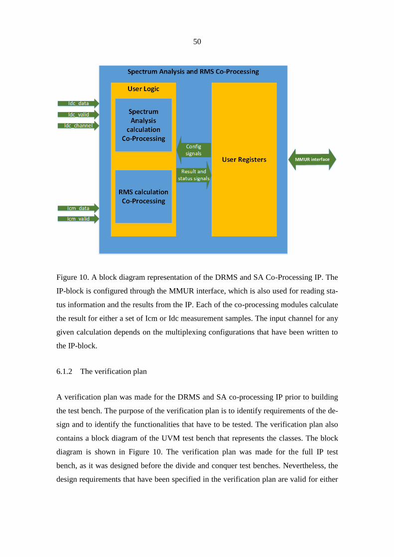
50
Figure 10. A block diagram representation of the DRMS and SA Co-Processing IP. The
IP-block is configured through the MMUR interface, which is also used for reading sta-
tus information and the results from the IP. Each of the co-processing modules calculate
the result for either a set of Icm or Idc measurement samples. The input channel for any
given calculation depends on the multiplexing configurations that have been written to
the IP-block.
6.1.2 The verification plan
A verification plan was made for the DRMS and SA co-processing IP prior to building
the test bench. The purpose of the verification plan is to identify requirements of the de-
sign and to identify the functionalities that have to be tested. The verification plan also
contains a block diagram of the UVM test bench that represents the classes. The block
diagram is shown in Figure 10. The verification plan was made for the full IP test
bench, as it was designed before the divide and conquer test benches. Nevertheless, the
design requirements that have been specified in the verification plan are valid for either
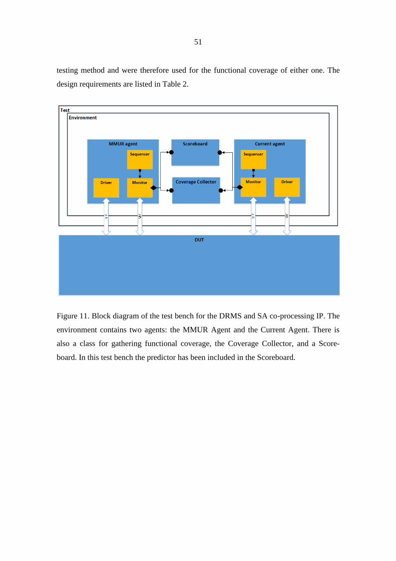
51
testing method and were therefore used for the functional coverage of either one. The
design requirements are listed in Table 2.
Figure 11. Block diagram of the test bench for the DRMS and SA co-processing IP. The
environment contains two agents: the MMUR Agent and the Current Agent. There is
also a class for gathering functional coverage, the Coverage Collector, and a Score-
board. In this test bench the predictor has been included in the Scoreboard.
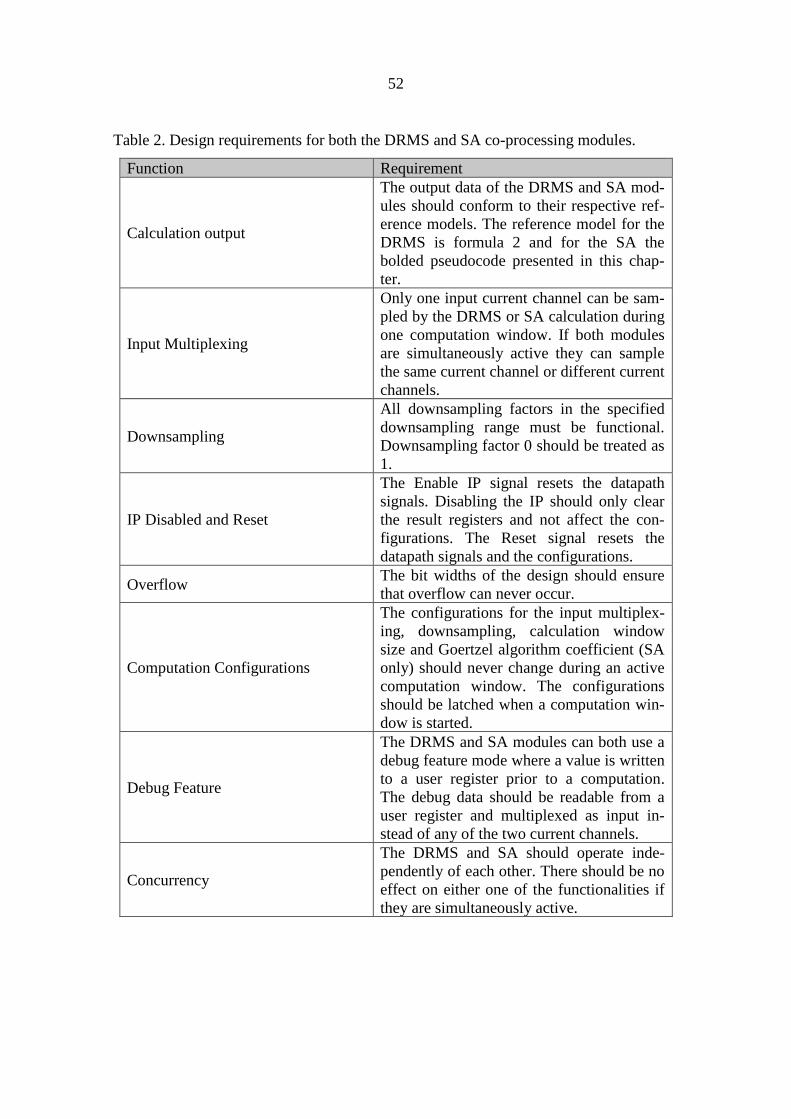
52
Table 2. Design requirements for both the DRMS and SA co-processing modules.
Function Requirement
Calculation output
The output data of the DRMS and SA mod-
ules should conform to their respective ref-
erence models. The reference model for the
DRMS is formula 2 and for the SA the
bolded pseudocode presented in this chap-
ter.
Input Multiplexing
Only one input current channel can be sam-
pled by the DRMS or SA calculation during
one computation window. If both modules
are simultaneously active they can sample
the same current channel or different current
channels.
Downsampling
All downsampling factors in the specified
downsampling range must be functional.
Downsampling factor 0 should be treated as
1.
IP Disabled and Reset
The Enable IP signal resets the datapath
signals. Disabling the IP should only clear
the result registers and not affect the con-
figurations. The Reset signal resets the
datapath signals and the configurations.
Overflow The bit widths of the design should ensure
that overflow can never occur.
Computation Configurations
The configurations for the input multiplex-
ing, downsampling, calculation window
size and Goertzel algorithm coefficient (SA
only) should never change during an active
computation window. The configurations
should be latched when a computation win-
dow is started.
Debug Feature
The DRMS and SA modules can both use a
debug feature mode where a value is written
to a user register prior to a computation.
The debug data should be readable from a
user register and multiplexed as input in-
stead of any of the two current channels.
Concurrency
The DRMS and SA should operate inde-
pendently of each other. There should be no
effect on either one of the functionalities if
they are simultaneously active.
53
6.1.3 The full IP test bench
Before building the classes of the UVM test bench the architecture of the test bench was
planned. The first action was to identify interfaces of coherent signals in the DUT.
Three interfaces were identified, as already described in Chapter 6.1.1. However, for
this case study both of the AD-measurement channels were combined to one agent – the
Current agent. The second agent of the test bench is the MMUR agent, which is used for
writing and reading to and from the user registers of the IP-block. The Current agent
drives samples from two separate measuring systems to the DUT in real hardware, and
could therefore also have been split into two agents. The amount of signals per current
interface, two for the Icm channel and three for the Idc channel, was however the reason
for combining the two interfaces into one agent. Figure 11 also shows that for this test
bench it was decided that the predictor model would reside inside the scoreboard.
Before implementing any classes, the requirements for the self-checking of the test
bench were determined. The scoreboard in this case is based on the In-Order Array
Scoreboard that was presented in Chapter 3.1.4. The In-Order type is preferred as the IP
always returns a response for one computation before another can be started. The In-
Order scoreboard furthermore requires the array as the results of both co-processing cal-
culations are split and stored in multiple registers of the IP. For this reason the predictor
model must also make multiple predictions per calculation. The implementation of this
case study does however differ slightly from the representation of Figure 4. Because the
full IP test bench requires that user registers containing the calculation results are
polled, the getkey()-function was excluded. The function is of no use in this case as
the register that is read is known and can directly be matched with the corresponding
prediction in the scoreboard.
6.1.4 Test cases of the full IP test bench
Before starting to build the test bench, test cases that validate the requirements of Table
2 were planned. The test cases, which will be described in the following paragraphs,
were all applicable to both co-processing modules. A user register write and read test
54
case was omitted in this case study as it had already been done for the IP with another
test bench.
A base test was implemented for both the DRMS and SA that follows the recommended
instructions for using either of the co-processing modules. In the base test the input mul-
tiplexing, downsampling factor, calculation window size and Goertzel algorithm coeffi-
cient (SA only) are all configured, after which a computation window is started by tog-
gling a start-bit in a control register. A status register is then polled that contains a bit to
signify a completed computation. The results are then read from the user registers and
compared to the predicted results.
A reset test was implemented to test the DUT when the reset signal is asserted at a ran-
dom time during a computation. The result registers are read after the reset and once
again after an invalid computation that hasn’t received new configurations has been
started. The latter computation should confirm that no configurations have been stored
in the user registers.
An IP disabling test was implemented to test the DUT when the IP is disabled at a
random time during a computation. The result registers are read after the IP is disabled.
The IP disabling sequence is followed by a normal computation window to confirm that
the DUT has recovered as expected.
The overflow test is intended to test that neither the DRMS or SA result registers over-
flow when worst case data is driven to either module. For the DRMS the worst case
scenario is when the maximum calculation window size is used and all current samples
have the value -215 . The value corresponds to the maximum negative value in the two’s
complement range for 16-bit signed values. For the SA the worst case scenario is
achieved when a maximal amplitude sine wave in the passband of the Goertzel algo-
rithm is driven to the DUT. For the Goertzel algorithm the passband equals the frequen-
cy bin that is analyzed, and it is dependent on the coefficient.

55
The reconfiguration test tests that the latching of computation window configurations
works as intended. The reconfiguration test randomly writes changed configurations to
the DUT once a computation window is already active. The DUT should ignore these
configurations.
The debug feature is tested with a debug data test. The test is identical to the base test
with the exception that the input multiplexers are configured to route the debug channel
into the DUT.
The final test that was implemented is a concurrency test where each of the co-
processing modules are simultaneously active. The test validates that the co-processing
modules can be used in parallel, either by starting the computation windows at the same
time or at separate times. The test also covers the case in which both co-processing
modules complete their computations at the same clock cycle.
Constrained randomization has been used in the tests for the DUT configurations, while
a simpler uniform randomization has been used for randomizing the time at which re-
configuration or disabling of the IP occurs. While all of the test cases are directed at a
design requirement, they all gather code coverage and functional coverage that is com-
mon and eventually merged. Because of the randomization the tests can be called multi-
ple times to raise coverage. Each test also has an arbitrary iteration count that can be
modified by the user. For instance, if high coverages are desired, a test could be as-
signed a high iteration count and be run outside working hours.
6.1.5 Building the full IP test bench
The designing phase of the test bench followed much of the same bottom-up order that
was introduced in Chapter 3.1.3. The classes seen in Figure 11 are described in the fol-
lowing paragraphs. Code segments have also been provided to give an insight of how
the functionality of each class has been implemented. The agent and environment clas-
ses have been excluded as they merely connect classes to each other.
56
The first classes that were designed were the sequence items. To understand how to
build the sequence item, however, the designer should first determine what sequences
the agent should drive. For the MMUR interface there is a write sequence, a read se-
quence and an idle sequence. The sequences are of variable length in terms of clock cy-
cles, but do not differ much in signal activity. In fact, it was determined that one se-
quence item could be used to build all sequences. The write enable and read enable
signals of the sequence item are assigned fixed values upon being created in the se-
quencer. The read sequence, for example, consists of three sequence items – one se-
quence item with an asserted read enable signal followed by two sequence items with
both write enable and read enable deasserted. The idle time of the sequence assures that
the DUT has enough time to handle the read request. The same functionality could also
have been implemented by the driver with a handshake task that waits for an
acknowledge input from the DUT to be asserted.
In the current agent the sequence models the behavior of the current measurement inter-
faces between the DUT and the Analog to Digital Converters (ADC). In the DUT of this
case study there are two separate current measurement interfaces. Both interfaces con-
tain two similar signals – a 16-bit signed type bit vector representing data and a one-bit
signal representing valid data. In addition, the Idc interface contains a signal that repre-
sents the AD-channel that the sample was measured from. Consequentially, the se-
quences of the two interfaces differ. The code segment below represents the task that
drives a sequence for the two current interfaces. In this example the signals of the Idc
interface have a prefix of Meas_.
//Omit class definition, constructor and irrelevant
//variables from this example
bit [3:0] channel;
int meas_ch_counter;
//For sampling frequency of 1.25 MHz when system clock
//is 100MHz: 100 MHz/1.25 MHz = 80.
const int Fs_period = 80;
//16 channels in the ADC of the Idc channel
const int Num_channel = 16;
task body();
57
Current_transaction tx;
channel = 0;
meas_ch_counter = 0;
for(int i=0; i<Fs_period; i++)
begin
if(i == 0)
begin
//Icm_vld_in asserted, Meas_vld_in asserted
tx = Current_transaction
::type_id::create(.name("tx "),
.contxt(get_full_name()));
start_item(tx);
assert(tx.randomize() with {
Meas_vld_in == 1;
Meas_ch_in == channel;
Icm_vld_in == 1;}
);
finish_item(tx);
end
else
begin
//Icm_vld_in deasserted, Meas_vld_in asserted
tx = Current_transaction
::type_id::create(.name("tx"),
.contxt(get_full_name()));
start_item(tx);
assert(tx.randomize() with {
Meas_vld_in == 1;
Meas_ch_in == channel;
Icm_vld_in == 0;}
);
finish_item(tx);
end
//Create Idc channel switching frequency of
//Fs_period/Num_channel clock cycles
if(meas_ch_counter == Fs_period/Num_channel-1)
begin
meas_ch_counter = 0;
if(channel== 15)
channel= 0;
else
channel++;
end
else
begin
meas_ch_counter++;
end
end
endtask: body

58
The preceding code segment creates the sequences that can be seen in Figure 12.
Figure 12. The sequences of the Icm and Idc current channels. The Icm channel drives a
valid sample at a frequency of 1.25 MHz. For the Idc channel the valid-signal stays as-
serted and a channel switching frequency of 78.125 kHz switches the sampling channel.
The sampling frequency for all Idc channels is therefore also 1.25 MHz. The DUT
stores the first Idc sample it detects after a channel switch and ignores other samples.
As there are no handshake requirements for either agent in this design, the drivers for
both agents are simple. In fact, both agents can share one driver implementation with
the only difference being the signals that are driven. The following code segment repre-
sents the task inside the driver of the current agent.
task drive();
Current_transaction tx;
forever begin
//Fetch the transaction from the sequencer
seq_item_port.get_next_item(tx);
vif.length = tx.length;
vif.delay = tx.delay;
//Initial delay before driving transaction
repeat(tx.delay)
@(posedge vif.Clk);
//Drive transaction
repeat(tx.length)begin
@(posedge vif.Clk)
vif.Meas_data_in <= tx.Meas_data_in;
vif.Meas_ch_in <= tx.Meas_ch_in;

59
vif.Meas_vld_in <= tx.Meas_vld_in;
vif.Icm_data_in <= tx.Icm_data_in;
vif.Icm_vld_in <= tx.Icm_vld_in;
end
//End transaction after tx.length clock cycles
seq_item_port.item_done();
end
endtask: drive
In the code segment above the length and delay variables have been added to the
driver to add flexibility. The delay variable can be used to insert an initial delay before
the transaction is driven. The length variable can be used to drive the transaction for
multiple clock cycles. Both of these are optional and can be constrained in the sequence
item to 0 and 1 respectively.
The next classes to be implemented were the monitors. Although the block diagram of
figure 10 only contains one monitor per agent, two monitors were actually implemented
for the MMUR agent. The MMUR agent contains one monitor that monitors transac-
tions when write enable or read enable are asserted and another that monitors transac-
tions when a read acknowledge signal is high. The aforementioned monitor writes to
both the coverage collector and the predictor in the scoreboard. The latter monitor
writes the actual DUT response to the scoreboard when the result registers are read. The
current agent only contains a monitor that writes to the coverage collector and the pre-
dictor. As there are two current interfaces there are also two monitoring threads that are
executed in a task. The threads trigger a write to the coverage collector and scoreboard
when their respective monitoring events occur. The two code segments below are, in
order, the run_phase task of the reading side MMUR monitor and the run_phase task
of the current monitor.
task run_phase(uvm_phase phase);
MMUR_transaction tx;
tx = MMUR_transaction
::type_id
::create(.name("tx"),
.contxt(get_full_name())
);
60
forever begin
@(posedge vif.Clk)
begin
if(vif.Mmur_re_ack_out == 1'b1)
begin
//Assign signals from virtual interface
//to the transaction tx
tx.Mmur_addr_in = vif.Mmur_addr_in;
//...
//Send the transaction to the analysis port
mon_ap_read.write(tx);
end
end
end
endtask: run_phase
In the above excerpt the monitoring event occurs when the read acknowledge signal is
asserted. The mon_ap_read.write(tx)statement writes the monitored event to the
analysis port that in turn forwards the transaction to the scoreboard.
task run_phase(uvm_phase phase);
tx_Idc = Current_transaction
::type_id
::create(.name("tx_Idc"),
.contxt(get_full_name())
);
tx_Icm = Current_transaction
::type_id
::create(.name("tx_Icm"),
.contxt(get_full_name())
);
int prev_ch;
fork
begin
//Monitoring thread for Idc
forever
begin
@(posedge vif.Clk)
if(vif.Meas_vld_in==1'b1&&(prev_ch!=vif.Meas_ch_in))
begin
//Delay for one clock cycle and sample data
@(posedge vif.Clk)
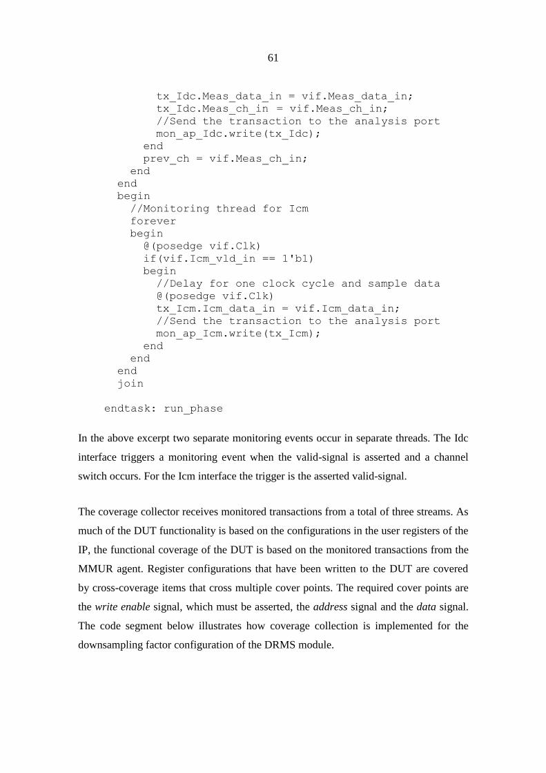
61
tx_Idc.Meas_data_in = vif.Meas_data_in;
tx_Idc.Meas_ch_in = vif.Meas_ch_in;
//Send the transaction to the analysis port
mon_ap_Idc.write(tx_Idc);
end
prev_ch = vif.Meas_ch_in;
end
end
begin
//Monitoring thread for Icm
forever
begin
@(posedge vif.Clk)
if(vif.Icm_vld_in == 1'b1)
begin
//Delay for one clock cycle and sample data
@(posedge vif.Clk)
tx_Icm.Icm_data_in = vif.Icm_data_in;
//Send the transaction to the analysis port
mon_ap_Icm.write(tx_Icm);
end
end
end
join
endtask: run_phase
In the above excerpt two separate monitoring events occur in separate threads. The Idc
interface triggers a monitoring event when the valid-signal is asserted and a channel
switch occurs. For the Icm interface the trigger is the asserted valid-signal.
The coverage collector receives monitored transactions from a total of three streams. As
much of the DUT functionality is based on the configurations in the user registers of the
IP, the functional coverage of the DUT is based on the monitored transactions from the
MMUR agent. Register configurations that have been written to the DUT are covered
by cross-coverage items that cross multiple cover points. The required cover points are
the write enable signal, which must be asserted, the address signal and the data signal.
The code segment below illustrates how coverage collection is implemented for the
downsampling factor configuration of the DRMS module.

62
cp_DOWNSAMPLING_RMS_data:
coverpoint tx_MMUR.Mmur_w_data_in[4:0]
{
//bins for the whole downsampling range
//all bins must be covered
bins corner_min = {0};
bins corner_1 = {1};
bins data = {[2:29]};
bins corner_29 = {30};
bins corner_max = {31};
}
cp_Mmur_we_in:
coverpoint tx_MMUR.Mmur_we_in
{
//only the TRUE-value of the write-enable signal
bins TRUE = {1};
}
cp_Mmur_addr_in:
coverpoint tx_MMUR.Mmur_addr_in
{
//bins for all enumerated type values
//corresponding to user register addresses
bins DOWNSAMPLING_FACTOR_REG =
{DOWNSAMPLING_FACTOR};
bins INPUT_SELECT_REG =
{INPUT_SELECT};
bins CALC_WINDOW_SIZE_REG =
{CALC_WINDOW_SIZE};
bins SPECTRUM_ANALYSIS_COEFF =
{SPECTRUM_ANALYSIS_COEFF};
}
Downsampling_RMS_cross:
cross
//this cross-coverage item crosses the following
//three coverpoints
cp_DOWNSAMPLING_RMS_data,
cp_Mmur_addr_in,
cp_Mmur_we_in
{
//cross-coverage that covers the minimum
//downsampling factor of the RMS calculation
bins RMS_cross_min =
binsof(cp_DOWNSAMPLING_RMS_data.corner_min) &&
binsof(cp_Mmur_addr_in.DOWNSAMPLING_FACTOR_REG)&&
binsof(cp_Mmur_we_in.TRUE);
}
In the above code three cover points are defined and a cross-coverage item is created for
downsampling factor 0. The cross-coverage item covers data that is written to the enu-
merated type address DOWNSAMPLING_FACTOR_REG.
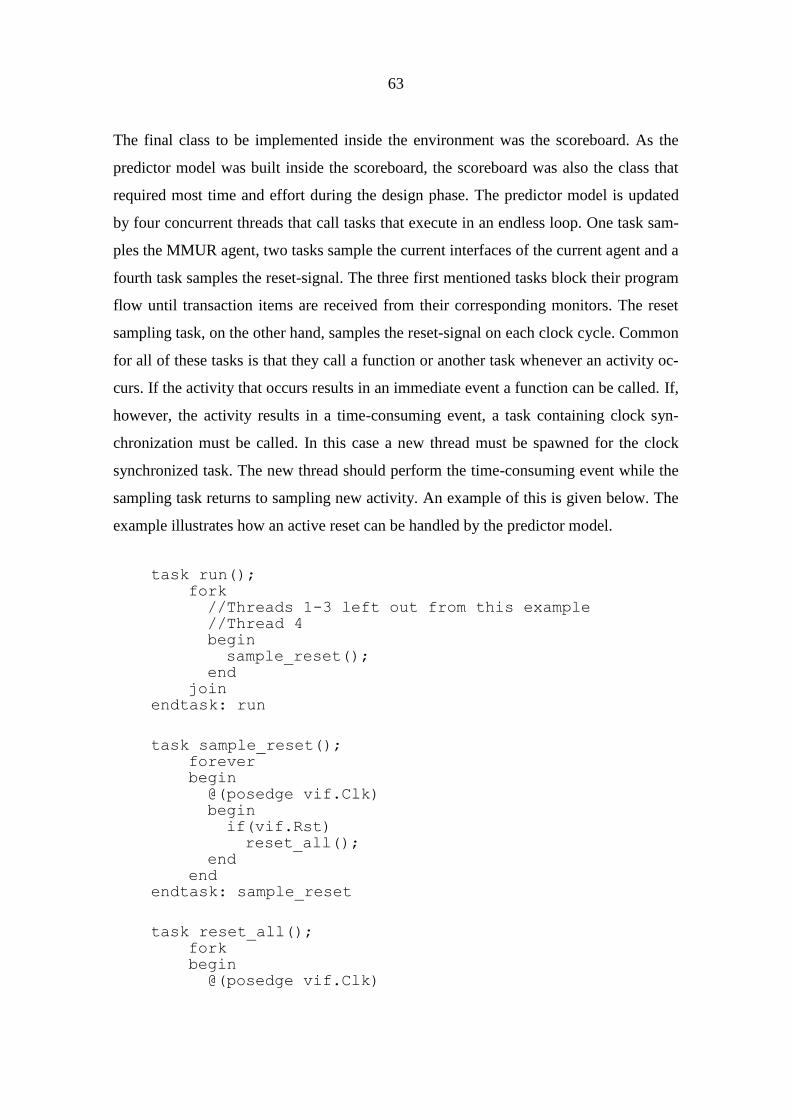
63
The final class to be implemented inside the environment was the scoreboard. As the
predictor model was built inside the scoreboard, the scoreboard was also the class that
required most time and effort during the design phase. The predictor model is updated
by four concurrent threads that call tasks that execute in an endless loop. One task sam-
ples the MMUR agent, two tasks sample the current interfaces of the current agent and a
fourth task samples the reset-signal. The three first mentioned tasks block their program
flow until transaction items are received from their corresponding monitors. The reset
sampling task, on the other hand, samples the reset-signal on each clock cycle. Common
for all of these tasks is that they call a function or another task whenever an activity oc-
curs. If the activity that occurs results in an immediate event a function can be called. If,
however, the activity results in a time-consuming event, a task containing clock syn-
chronization must be called. In this case a new thread must be spawned for the clock
synchronized task. The new thread should perform the time-consuming event while the
sampling task returns to sampling new activity. An example of this is given below. The
example illustrates how an active reset can be handled by the predictor model.
task run();
fork
//Threads 1-3 left out from this example
//Thread 4
begin
sample_reset();
end
join
endtask: run
task sample_reset();
forever
begin
@(posedge vif.Clk)
begin
if(vif.Rst)
reset_all();
end
end
endtask: sample_reset
task reset_all();
fork
begin
@(posedge vif.Clk)
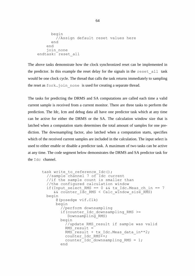
64
begin
//Assign default reset values here
end
end
join_none
endtask: reset_all
The above tasks demonstrate how the clock synchronized reset can be implemented in
the predictor. In this example the reset delay for the signals in the reset_all task
would be one clock cycle. The thread that calls the task returns immediately to sampling
the reset as fork…join_none is used for creating a separate thread.
The tasks for predicting the DRMS and SA computations are called each time a valid
current sample is received from a current monitor. There are three tasks to perform the
prediction. The Idc, Icm and debug data all have one predictor task which at any time
can be active for either the DRMS or the SA. The calculation window size that is
latched when a computation starts determines the total amount of samples for one pre-
diction. The downsampling factor, also latched when a computation starts, specifies
which of the received current samples are included in the calculation. The input select is
used to either enable or disable a predictor task. A maximum of two tasks can be active
at any time. The code segment below demonstrates the DRMS and SA predictor task for
the Idc channel.
task write_to_reference_Idc();
//sample channel 7 of Idc current
//if the sample count is smaller than
//the configured calculation window
if(Input_select_RMS == 0 && tx_Idc.Meas_ch_in == 7
&& counter_Idc_RMS < Calc_window_size_RMS)
begin
@(posedge vif.Clk)
begin
//perform downsampling
if(counter_Idc_downsampling_RMS >=
Downsampling_RMS)
begin
//update RMS_result if sample was valid
RMS_result =
RMS_result + tx_Idc.Meas_data_in**2;
counter_Idc_RMS++;
counter_Idc_downsampling_RMS = 1;
end
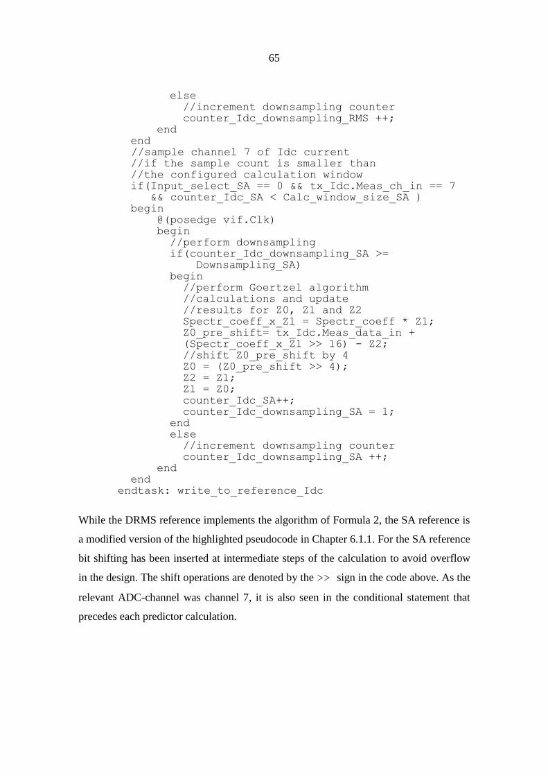
65
else
//increment downsampling counter
counter_Idc_downsampling_RMS ++;
end
end
//sample channel 7 of Idc current
//if the sample count is smaller than
//the configured calculation window
if(Input_select_SA == 0 && tx_Idc.Meas_ch_in == 7
&& counter_Idc_SA < Calc_window_size_SA )
begin
@(posedge vif.Clk)
begin
//perform downsampling
if(counter_Idc_downsampling_SA >=
Downsampling_SA)
begin
//perform Goertzel algorithm
//calculations and update
//results for Z0, Z1 and Z2
Spectr_coeff_x_Z1 = Spectr_coeff * Z1;
Z0_pre_shift= tx_Idc.Meas_data_in +
(Spectr_coeff_x_Z1 >> 16) - Z2;
//shift Z0_pre_shift by 4
Z0 = (Z0_pre_shift >> 4);
Z2 = Z1;
Z1 = Z0;
counter_Idc_SA++;
counter_Idc_downsampling_SA = 1;
end
else
//increment downsampling counter
counter_Idc_downsampling_SA ++;
end
end
endtask: write_to_reference_Idc
While the DRMS reference implements the algorithm of Formula 2, the SA reference is
a modified version of the highlighted pseudocode in Chapter 6.1.1. For the SA reference
bit shifting has been inserted at intermediate steps of the calculation to avoid overflow
in the design. The shift operations are denoted by the >> sign in the code above. As the
relevant ADC-channel was channel 7, it is also seen in the conditional statement that
precedes each predictor calculation.

66
6.1.6 Building the divide and conquer test benches
The main interest of the divide and conquer method was to determine whether a fully
randomized test could be made with a reasonable design effort. As stated previously, the
full randomization in this context would mean a single test case in which the sequence
of events is randomized. A fully randomized test case minimizes the amount of time
required for writing test cases and can be adjusted by modifying the constraints of the
sequences. A fully randomized test should also be able to reveal corner cases not con-
sidered by the designer of the test bench. The divide and conquer method of this case
study was performed after the full IP test bench case study had been completed.
During the design phase of the full IP test bench it was identified that a full randomiza-
tion would require additional functionality in some of the test bench classes, namely for
reset awareness. Other changes that would be beneficial for the test bench structure
were also observed, such as creating an agent for the reset signal, splitting the Idc and
Icm interfaces into two agents and creating predictors for the DRMS and SA modules in
classes outside the scoreboard. It was also decided that clock synchronization would be
excluded from the predictors and instead implemented at a lower level in the monitors.
The case study of the divide and conquer method has been implemented for the user
logic test bench as it was deemed to be adequate for demonstrating a fully randomized
test. The following paragraphs will detail the added functionalities that are required by a
fully randomized test bench. The block diagram of the test bench is depicted in Figure
13. Figure 14 shows the connections to the classes outside of the agents that reside in
the environment: the RMS predictor, the SA predictor, the coverage collector and the
scoreboard.

67
Figure 13. Block diagram for the user logic test bench of the DRMS and SA co-
processing IP. In this figure the analysis ports from the monitors to the four classes in
the environment have been left out for the sake of clarity. The connections to these four
classes have been illustrated in Figure 14. As in Figure 11, some monitors have been
depicted as one block although two monitor classes have been designed in the agent.
The agents with two monitors are the RMS agent and the SA agent.
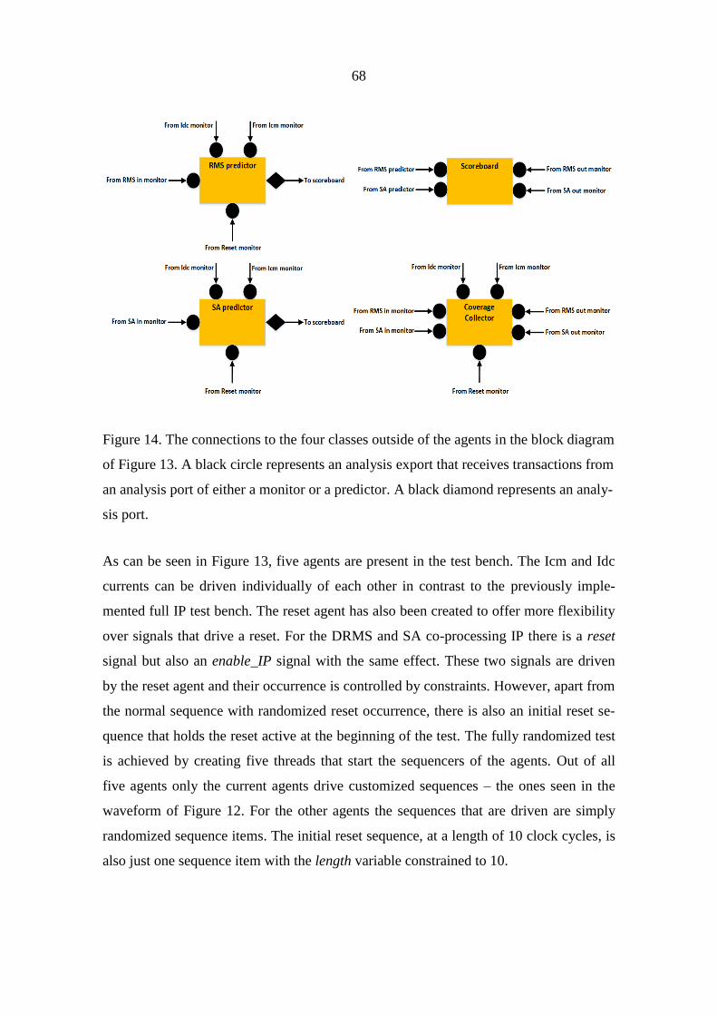
68
Figure 14. The connections to the four classes outside of the agents in the block diagram
of Figure 13. A black circle represents an analysis export that receives transactions from
an analysis port of either a monitor or a predictor. A black diamond represents an analy-
sis port.
As can be seen in Figure 13, five agents are present in the test bench. The Icm and Idc
currents can be driven individually of each other in contrast to the previously imple-
mented full IP test bench. The reset agent has also been created to offer more flexibility
over signals that drive a reset. For the DRMS and SA co-processing IP there is a reset
signal but also an enable_IP signal with the same effect. These two signals are driven
by the reset agent and their occurrence is controlled by constraints. However, apart from
the normal sequence with randomized reset occurrence, there is also an initial reset se-
quence that holds the reset active at the beginning of the test. The fully randomized test
is achieved by creating five threads that start the sequencers of the agents. Out of all
five agents only the current agents drive customized sequences – the ones seen in the
waveform of Figure 12. For the other agents the sequences that are driven are simply
randomized sequence items. The initial reset sequence, at a length of 10 clock cycles, is
also just one sequence item with the length variable constrained to 10.

69
In the divide and conquer case study more design effort was put into the monitors of the
agents. The objective was to create monitors that would allow clock synchronization to
be excluded from the predictors. By doing so the classes outside of the agents would all
be modeled on the transaction level, which would arguably be easier to comprehend for
an engineer not familiar with the specific timing of the DUT. In the full IP test bench
the reset awareness of the test bench has been implemented in the predictor model of the
scoreboard. In this case study the same functionality has been moved to the monitors.
An example of this is given in the following code segment from the RMS output moni-
tor. In the code segment the analysis port corresponding to the DUT response can be
written to only when the reset is deasserted. A task inside the RMS output monitor con-
tinuously monitors the state of the reset signal. An active reset will nullify a calculation
event in the DUT and therefore it is not desired that a DUT response is written to the
scoreboard when the reset is asserted. In the predictor the predicted response for the
same calculation event will similarly be cleared once the monitor of the reset agent sig-
nals that the reset is asserted.
task run_phase(uvm_phase phase);
RMS_transaction tx;
tx = RMS_transaction
::type_id
::create(.name("tx"),
.contxt(get_full_name())
);
fork
begin
forever
begin
@(posedge vif.Clk)
begin
if(vif.Rms_done_out &&
Rms_done_out_prev != vif.Rms_done_out &&
!reset_asserted && Rms_calc_size > 0)
begin
//Monitor signals that are received from the DUT
tx.Rms_result_msb_out
= vif.Rms_result_msb_out;
tx.Rms_result_lsb_out
= vif.Rms_result_lsb_out;
//Send the transaction to the analysis port
mon_ap_out.write(tx);
end
70
//Edge detection for ‘done_out’ signal
//Only write to analysis port on rising edge
Rms_done_out_prev = vif.Rms_done_out;
end
end
end
begin
forever
begin
@(posedge vif.Clk)
begin
fork
//Call task that monitors reset
//and enable_IP signal
//Reset is asserted/deasserted
//with a latency of 3 clock cycles
assert_reset();
join_none
end
end
end
join_any
endtask: run_phase
In this case study the predictors for the DRMS and SA modules were created as separate
classes outside the scoreboard. The reason behind this decision was modularity. During
the full IP test bench case study it was observed that the amount of code in the score-
board grew significantly when the predictors of both the DRMS and SA modules were
implemented inside the scoreboard class. In addition, the purpose of the tasks and func-
tions inside the scoreboard were not trivial – tasks and functions for both prediction and
comparison were written inside the same class. In this case study the scoreboard only
does the comparison and keeps track of the amount of successful and erroneous compar-
isons. The comparisons have been implemented as in Figure 3 and they are triggered
when either the RMS out or SA out monitors send a transaction to the scoreboard.
As stated in Chapter 5.3, fully randomized tests require functional coverage items for
events that must be tested. As one calculation window for either the DRMS or SA co-
processing may last for as much as 20 ms, the probability for an asserted reset or deas-
serted enable_IP has been set to 1 in 10000000 sequence items. This probability was
chosen once it was discovered that higher probabilities caused too many interrupts, es-
pecially for calculation events with longer calculation windows. However, at this prob-

71
ability the time before a reset occurs may be as much as several hours of simulation, and
there is no guarantee that such event occurs for one iteration of the test. Functional cov-
erage items are therefore written to ensure that resets have been tested when a calcula-
tion is active for the DRMS or the SA module, but also when either of the modules are
idle. The method for implementing such coverage is cross-coverage. In this case two
cross-coverage items were created – one for the reset signal and another for the ena-
ble_IP signal. The cover points for these signals are crossed with two local variables in
the coverage collector that signify whether a calculation is active or not in the DRMS or
the SA module. The calculation_active_RMS and calculation_active_SA variables are
set to true whenever a transaction signaling a starting calculation is received from the
RMS_in or SA_in analysis exports depicted in Figure 14. Conversely, the variables are
set to false whenever a transaction signaling a completed calculation is received from
the RMS_out or SA_out analysis exports. The variables are also set to false if a transac-
tion is received from the Reset analysis export. The reset functionality of the DUT can
be considered fully tested only when the functional coverage for the reset and enable_IP
cross-coverage items is 100%.
6.2 Testing the priority arbitrated full-duplex communication SUT
The case study of the system wide test is implemented as a SystemVerilog test bench
for which randomization and the utilization of UVM has been excluded. As mentioned
in Chapter 5.2, the communication with the embedded processors of two separate FPGA
nodes has been modeled with AXI BFMs provided by FPGA manufacturer Xilinx. In
order to simulate a system wide FPGA design, the embedded processors of the design
are removed from the system and replaced by BFMs. The amount of BFMs and their
type depend on the processors. In the SUT of this case study three types of AXI BFMs
are used: the AXI4-Lite BFM, the AXI4-Stream BFM and the AXI3 BFM. The BFMs
are provided as agents and are similar in structure to the UVM agent described in Chap-
ter 2.1.3. Although UVM is not used in this case study, the objective is to create a test
bench that benefits from a test bench architecture that is common for object-oriented
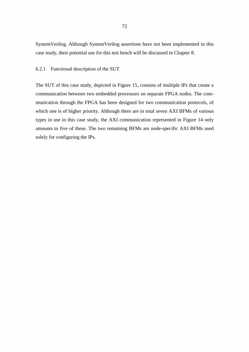
72
SystemVerilog. Although SystemVerilog assertions have not been implemented in this
case study, their potential use for this test bench will be discussed in Chapter 8.
6.2.1 Functional description of the SUT
The SUT of this case study, depicted in Figure 15, consists of multiple IPs that create a
communication between two embedded processors on separate FPGA nodes. The com-
munication through the FPGA has been designed for two communication protocols, of
which one is of higher priority. Although there are in total seven AXI BFMs of various
types in use in this case study, the AXI communication represented in Figure 14 only
amounts to five of these. The two remaining BFMs are node-specific AXI BFMs used
solely for configuring the IPs.
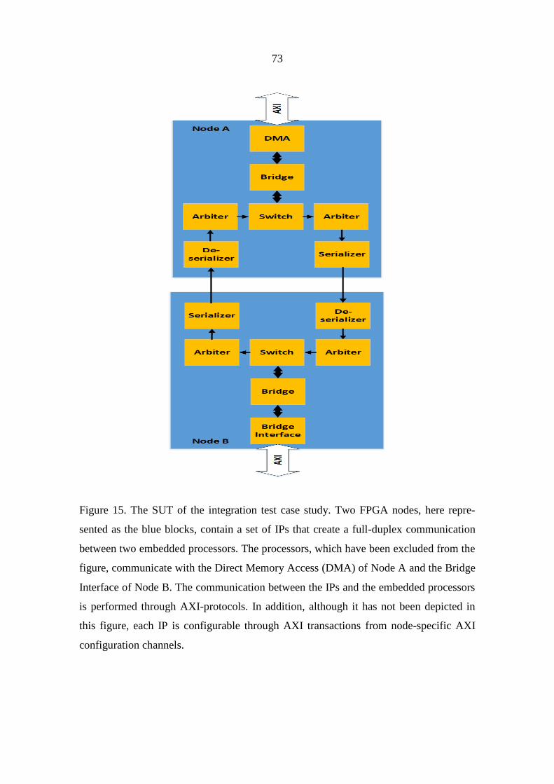
73
Figure 15. The SUT of the integration test case study. Two FPGA nodes, here repre-
sented as the blue blocks, contain a set of IPs that create a full-duplex communication
between two embedded processors. The processors, which have been excluded from the
figure, communicate with the Direct Memory Access (DMA) of Node A and the Bridge
Interface of Node B. The communication between the IPs and the embedded processors
is performed through AXI-protocols. In addition, although it has not been depicted in
this figure, each IP is configurable through AXI transactions from node-specific AXI
configuration channels.

74
The DMA of the Node A in Figure 15 communicates with an AXI3 BFM that is config-
ured as a slave agent. The DMA, being the master of a master-slave communication be-
tween itself and the processor, would in the real design initiate read requests to access
the cache of the processor. In the simulation, however, the cache has been modeled by a
SystemVerilog associative array that is indexed by the address signal of the AXI trans-
action. The data is initialized into the array before the simulation is run and it is a task
of the driver component of the AXI3 slave agent to respond to read requests with valid
data. The DMA is configured by a node-specific AXI4-Lite master agent and contains,
among other registers, a register that is written to whenever DMA transmissions are de-
sired. Other IPs inside Node A are configured by the same AXI4-Lite master agent.
The embedded processor of Node B has in this case study been modeled by five sepa-
rate BFMs. As for Node A, an AXI4-Lite master agent writes configurations to the var-
ious IPs inside the node. The actual communication of Node A embedded processor is
modeled by four AXI4-Stream BFMs. Two of these are configured as master agents
while the other two are configured as slave agents. In contrast to the AXI3 or AXI4 pro-
tocols, the dataflow of the AXI4-Stream protocol is unidirectional. Consecutively, the
two master agents of Node B transmit data towards the FPGA while the slave agents
receive data from it.
6.2.2 The verification plan
As for the IP-block tests, requirements of the design were determined before starting the
building phase of the test bench. Performance-related requirements such as throughput
or latency of the communication have not been addressed at this verification layer. In-
stead, such metrics are tested and verified on a higher level that includes the firmware of
the device. The requirements of the design that are addressed by the test bench of this
case study are listed in Table 4.
75
Table 4. Design requirements for the priority arbitrated full-duplex communication of
the SUT.
Function Requirement
Message validity
The content of a received message should
match with that of a message that has been
sent.
Concurrency
The system should be able to transmit or
receive multiple simultaneously active mes-
sages with the same destination.
Message routing
Messages received at either the DMA of
Node A or the Bridge Interface of Node B
should be stored in the correct buffer of ei-
ther IP. The buffer selection is based on
routing configurations that are software
configurable.
Uninterrupted communication
Deadlocks, which for this system could oc-
cur as a result of faulty buffer multiplexing,
should never occur.
Priority arbitration
If two messages of different priorities are
sent simultaneously, the message with the
higher priority should be received at the
destination first.
Out of all requirements listed in Table 4, the priority arbitration is perhaps a require-
ment that should have been tested on the IP block level. Arbitration is done by the arbi-
ter IP that can be seen in Figure 15, however, a priority multiplexing is also implement-
ed on the Bridge Interface of Node B. These are features that would arguably be easier
to test extensively on the IP-block level with constrained randomization and assertions.
In a system level test visibility into the SUT is limited, and in addition, the propagation
delay through the IPs preceding the arbiter is nondeterministic. Testing the priority arbi-
tration will therefore not be a focus of this case study. For the remaining design re-
quirements, two system level tests were designed – one for transmitting messages from
Node A to Node B and another for transmitting messages in the other direction. The re-
quirement of concurrency would of course dictate that a third test should be designed
with communication occurring in both directions concurrently. This test was however
left out of this case study to limit the workload. Although tests have been implemented
for communication in either direction, Node A to Node B and vice versa, only the Node
B to Node A test will be described in detail. The second test case relies on the same de-
76
sign principles and its implementation details have therefore been excluded from this
thesis. The Node B to Node A test will from here on be referred to simply as the
NBNA-test. The other test case will be referred to as the NANB-test.
6.2.3 Building the NBNA-test
To achieve a communication from the embedded processor of Node B to the embedded
processor Node A, a test bench with the structure depicted in Figure 16 was built. The
various AXI agents inside the test bench block of the figure simulate the processors.
Figure 16. The block diagram depiction of the NBNA test bench. For this test a total of
five AXI BFMs are required to model the behavior of the embedded processors. In the
NANB-test the only difference in the test bench architecture is in the two AXI4-Stream
agents communicating with the Node B, which are instead slave agents.

77
As in the UVM test benches of the IP-block level tests, the top module of this case
study has been made simple. The top module oscillates a clock at 50 MHz and toggles
the initial reset. These signals are also connected to the top module of the SUT. The
tests, however, are initiated as objects. One object is initiated for the NBNA class, an-
other for the NANB class. The configuration of the SUT as well as the driving and mon-
itoring of stimulus is performed inside the test classes. The test classes also contain
tasks for self-checking received messages against messages that have been sent. A test
is run inside a test object until all messages are received or until a timeout error occurs.
The following code segment illustrates how the top module declares the test objects and
starts the test. The top module contains an initial block with a test sequence that is easy
to comprehend.
//Declare an object for each test
NANB test_1; //Node A to Node B
NBNA test_2; //Node B to Node A
initial
begin
$display("Starting Node A to Node B transmit
test\n");
test_1 = new;
test_1.run_test();
$display("Finishing Node A to Node B
transmit test\n");
$display("Starting Node B to Node A
transmit test\n");
test_2 = new;
test_2.run_test();
$display("Finishing Node B to Node A
transmit test\n");
end
As can be seen in the code segment above, the object is created with a call to the con-
structor of the test class. In many programming languages the constructor initializes var-
iables with default values. In this case, however, the variable initializations have been
made in a separate package that is specific for the test. The main reason behind this de-
cision is the amount of variables that are required by the five AXI interfaces of the test
bench. In addition, for most variables zero suffices as a default value. The constructor is
instead used for initializing two parametrizable arrays with data. The data inside the ar-
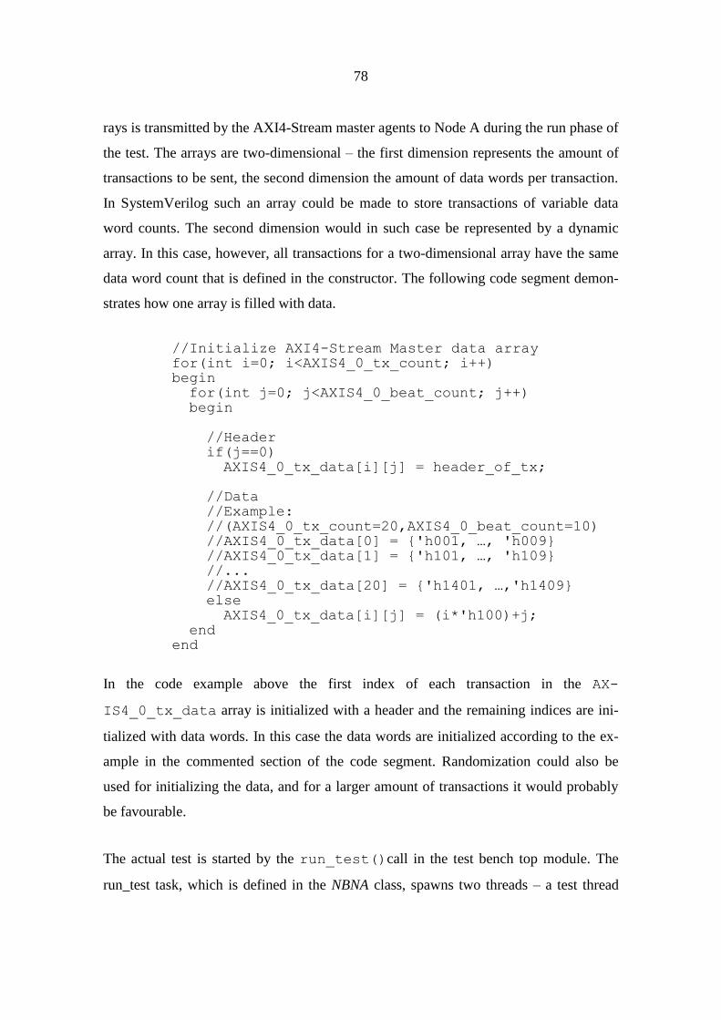
78
rays is transmitted by the AXI4-Stream master agents to Node A during the run phase of
the test. The arrays are two-dimensional – the first dimension represents the amount of
transactions to be sent, the second dimension the amount of data words per transaction.
In SystemVerilog such an array could be made to store transactions of variable data
word counts. The second dimension would in such case be represented by a dynamic
array. In this case, however, all transactions for a two-dimensional array have the same
data word count that is defined in the constructor. The following code segment demon-
strates how one array is filled with data.
//Initialize AXI4-Stream Master data array
for(int i=0; i<AXIS4_0_tx_count; i++)
begin
for(int j=0; j<AXIS4_0_beat_count; j++)
begin
//Header
if(j==0)
AXIS4_0_tx_data[i][j] = header_of_tx;
//Data
//Example:
//(AXIS4_0_tx_count=20,AXIS4_0_beat_count=10)
//AXIS4_0_tx_data[0] = {'h001, …, 'h009}
//AXIS4_0_tx_data[1] = {'h101, …, 'h109}
//...
//AXIS4_0_tx_data[20] = {'h1401, …,'h1409}
else
AXIS4_0_tx_data[i][j] = (i*'h100)+j;
end
end
In the code example above the first index of each transaction in the AX-
IS4_0_tx_data array is initialized with a header and the remaining indices are ini-
tialized with data words. In this case the data words are initialized according to the ex-
ample in the commented section of the code segment. Randomization could also be
used for initializing the data, and for a larger amount of transactions it would probably
be favourable.
The actual test is started by the run_test()call in the test bench top module. The
run_test task, which is defined in the NBNA class, spawns two threads – a test thread
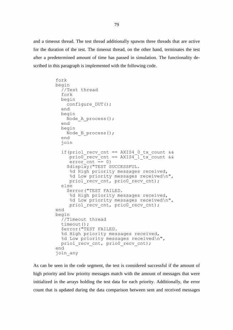
79
and a timeout thread. The test thread additionally spawns three threads that are active
for the duration of the test. The timeout thread, on the other hand, terminates the test
after a predetermined amount of time has passed in simulation. The functionality de-
scribed in this paragraph is implemented with the following code.
fork
begin
//Test thread
fork
begin
configure_DUT();
end
begin
Node_A_process();
end
begin
Node_B_process();
end
join
if(prio1_recv_cnt == AXIS4_0_tx_count &&
prio0_recv_cnt == AXIS4_1_tx_count &&
error_cnt == 0)
$display("TEST SUCCESSFUL.
%d High priority messages received,
%d Low priority messages received\n",
prio1_recv_cnt, prio0_recv_cnt);
else
$error("TEST FAILED.
%d High priority messages received,
%d Low priority messages received\n",
prio1_recv_cnt, prio0_recv_cnt);
end
begin
//Timeout thread
timeout();
$error("TEST FAILED.
%d High priority messages received,
%d Low priority messages received\n",
prio1_recv_cnt, prio0_recv_cnt);
end
join_any
As can be seen in the code segment, the test is considered successful if the amount of
high priority and low priority messages match with the amount of messages that were
initialized in the arrays holding the test data for each priority. Additionally, the error
count that is updated during the data comparison between sent and received messages

80
must be null. If the transaction counts do not match or if the error count differs from ze-
ro, the test is considered unsuccessful and an error message is printed. The same is true
if the test does not finish within the time specified in the timeout task. The data com-
parison is performed in the Node_A_process task.
The Node_B_process and Node_A_process are, in order, the tasks that send and
receive messages. They will from here on be referred to as the node tasks. The con-
figure_DUT task is where all configurations are written to the nodes. The DUT con-
figurations are written to each node concurrently, and in this case, a SystemVerilog
event is used to synchronize the configuration commands of Node B with its node task
that drives the stimulus. The task should wait until the node configurations are written
before starting to send data. This information is made available to the task through the
activation of Node B configuration event. The Node_A_process task, on the other hand,
starts its activity at the moment the test is started. Both of the node tasks are based on
functions provided by the AXI BFMs. The full syntax inside the tasks is not important
in order to understand the functionality of the test, and therefore much of the code has
been removed from the following code segments. The code segments represent the key
features of the node tasks.
@(Node_B_configured);
#15000; //Wait for system to stabilize.
fork
begin
//AXI4-STREAM MASTER 0 DRIVER
//Thread for driving high priority
//transactions from AXI4-STREAM master agent 0.
for(int i=0; i<AXIS4_0_tx_count; i++)
begin
#delay;
for(int j=0; j<AXIS4_0_beat_count; j++)
begin
wr_transaction_0 =
mst_agent_axis4_0_power.driver.
create_transaction
("MST AXI4-STREAM VIP 0 write tx");
wr_transaction_0.

81
set_data_beat(AXIS4_0_tx_data[i][j]);
wr_transaction_0.set_delay(0);
if(j==AXIS4_0_beat_count-1)
wr_transaction_0.set_last(1);
end
end
end
begin
//AXI4-STREAM MASTER 1 DRIVER
//Thread for driving low priority
//transactions from AXI4-STREAM master agent 1.
//Transactions sent as for AXI4-STREAM MASTER 0.
//See for-loop above.
end
begin
//AXI4 STREAM MASTER 0 MONITOR
//Thread for monitoring high priority
//transactions sent from
//AXI4-STREAM MASTER 0 DRIVER
while(mst_agent_axis4_0_tx_queue_size <
AXIS4_0_tx_count)
begin
mst_agent_axis4_0_power.monitor.
item_collected_port.
get(mst_agent_axis4_0_tx);
mst_agent_axis4_0_tx_queue.
push_back(mst_agent_axis4_0_tx);
mst_agent_axis4_0_tx_queue_size++;
end
end
begin
//AXI4 STREAM MASTER 1 MONITOR
//Thread for monitoring low priority
//transactions sent from
//AXI4-STREAM MASTER 0 DRIVER
//Transactions monitored as for
//AXI4-STREAM MASTER 0.
//See while-loop above.
end
join
$display("Node B Process finished\n");
The above code segment demonstrates how two AXI4-Stream drivers are used in master
mode to drive data to the SUT, and how two monitors store the transactions that are sent
to a queue. In this example the AXI4-Stream Master 0 Driver drives the high priority

82
messages at an time interval equivalent to the delay time-variable. The monitor for the
same master agent stalls the execution of its while-loop with the get-statement until a
transaction is sent from the driver. The Node_B_process task finishes once all transac-
tions have been sent from the drivers and all transactions have been stored into the mon-
itor queues.
The purpose of the Node_A_process task, as has already been stated, is to receive the
messages and to do the comparison. For receiving the messages through the AXI3 inter-
face, a thread must be spawned for a monitor, but one should also be spawned for a
slave driver. In addition, a third thread is spawned for the data comparison, here referred
to as the scoreboard thread. This thread utilizes methods of the AXI BFM package as it
needs to extract the data payload as well as other information from the transactions that
are received by the monitor. The code below demonstrates the key features of the
Node_A_process task.
fork
begin
//AXI3 SLAVE DRIVER
//Thread for sending a reactive handshake
//transaction to the DMA controller
//of Node A.
while(prio1_received + prio0_received <
mst_agent_axis4_0_tx_queue_size +
mst_agent_axis4_1_tx_queue_size)
begin
slv_agent_axi3_control.wr_driver.
get_wr_reactive(reactive_transaction);
fill_reactive(reactive_transaction);
slv_agent_axi3_control.wr_driver.
send(reactive_transaction);
end
end
begin
//AXI3 SLAVE MONITOR
//Thread for monitoring the high priority and
//low priority transactions received from the
//DMA controller.
while(prio1_received + prio0_received <
mst_agent_axis4_0_tx_queue_size +
mst_agent_axis4_1_tx_queue_size)
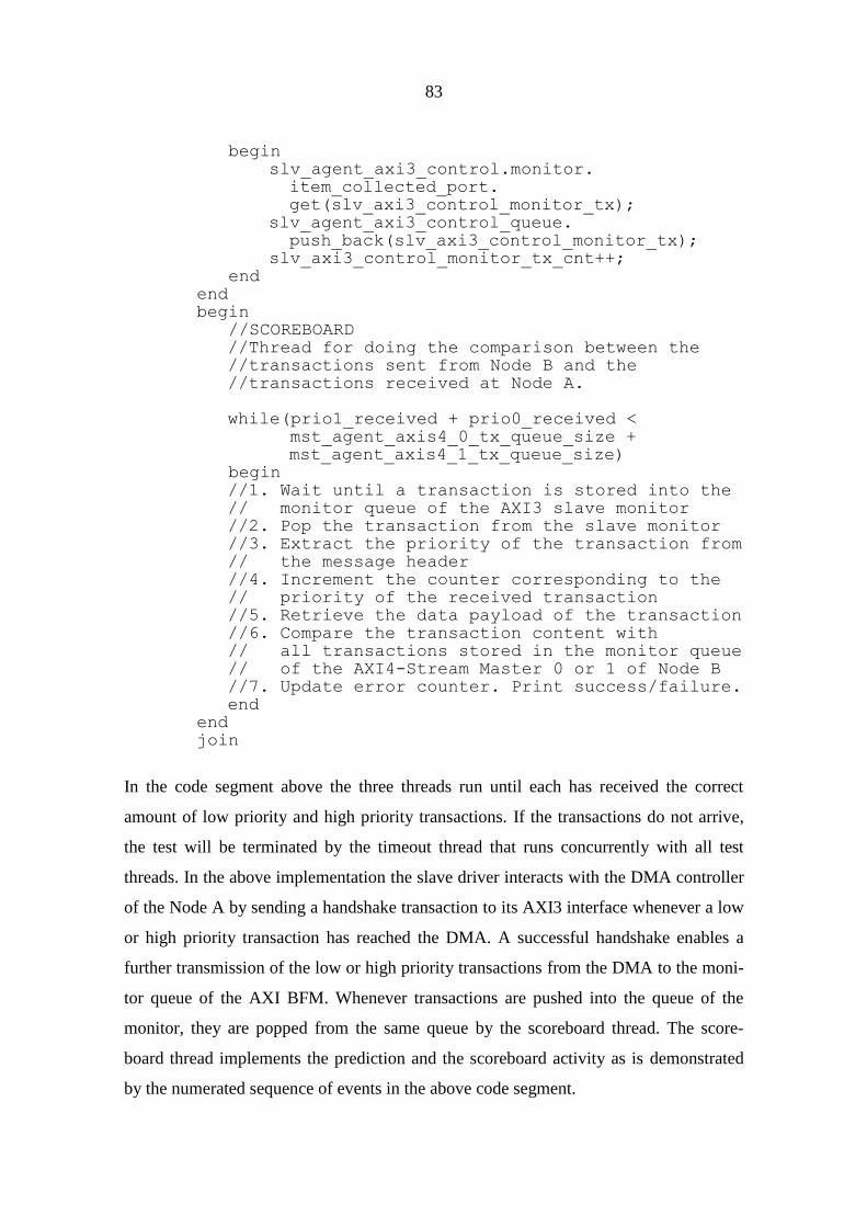
83
begin
slv_agent_axi3_control.monitor.
item_collected_port.
get(slv_axi3_control_monitor_tx);
slv_agent_axi3_control_queue.
push_back(slv_axi3_control_monitor_tx);
slv_axi3_control_monitor_tx_cnt++;
end
end
begin
//SCOREBOARD
//Thread for doing the comparison between the
//transactions sent from Node B and the
//transactions received at Node A.
while(prio1_received + prio0_received <
mst_agent_axis4_0_tx_queue_size +
mst_agent_axis4_1_tx_queue_size)
begin
//1. Wait until a transaction is stored into the
// monitor queue of the AXI3 slave monitor
//2. Pop the transaction from the slave monitor
//3. Extract the priority of the transaction from
// the message header
//4. Increment the counter corresponding to the
// priority of the received transaction
//5. Retrieve the data payload of the transaction
//6. Compare the transaction content with
// all transactions stored in the monitor queue
// of the AXI4-Stream Master 0 or 1 of Node B
//7. Update error counter. Print success/failure.
end
end
join
In the code segment above the three threads run until each has received the correct
amount of low priority and high priority transactions. If the transactions do not arrive,
the test will be terminated by the timeout thread that runs concurrently with all test
threads. In the above implementation the slave driver interacts with the DMA controller
of the Node A by sending a handshake transaction to its AXI3 interface whenever a low
or high priority transaction has reached the DMA. A successful handshake enables a
further transmission of the low or high priority transactions from the DMA to the moni-
tor queue of the AXI BFM. Whenever transactions are pushed into the queue of the
monitor, they are popped from the same queue by the scoreboard thread. The score-
board thread implements the prediction and the scoreboard activity as is demonstrated
by the numerated sequence of events in the above code segment.

84
7 RESULTS
7.1 Results of the full IP test bench case study
In this case study the DUT was considered sufficiently tested once all tests were per-
formed and the functional coverage was 100%. To reach full functional coverage the
initial implementation for the coverage collector of the test bench had to be modified, as
it was discovered early during the testing that simulation of the DUT would be time
consuming. Large calculation window sizes with high downsampling factors resulted in
computations that lasted for as much as one day. Corner cases for the computation con-
figurations were therefore identified to ensure that critical features of the DUT would be
tested. Additionally, the amount of coverage bins per computation configuration was
reduced for configurations with a wide range of possible values. In order to achieve suf-
ficient functional coverage, the constraints for the randomized stimulus also had to be
modified. The functional coverage for the computation configurations are listed in Table
5 below. Unless otherwise stated, the bins for each computation configuration in the ta-
ble are valid for both the DRMS and the SA co-processing modules.
Table 5. Functional coverage for each computation configuration. Bins representing
ranges are represented as minimum:maximum. Due to time consuming simulations the
amount of hits required per bin is simply one. It is however identified that the amount of
required hits, especially for bins with a range of values, should have been larger.

85
Computation Configuration Functional Coverage
Input Select 1 cover point with 4 bins : {0, 1, 2, 3}
(0 = Idc, 1 = Icm, 2 = Debug input, 3 = Idc)
Calculation Window Size 1 cover point with 5 bins :
{0, 1, 2:24998, 24999, 25000}
Downsampling Factor 1 cover point with 5 bins :
{0, 1, 2:29, 30, 31}
Goertzel Algorithm Coefficient
(17-bit signed, two’s complement)
Spectrum Analyzer only
1 cover point with 7 bins :
{-65536, -65535:(-2), -1, 0, 1, 2:65534,
65535}
As demonstrated in Chapter 6.1.5, the computation configurations are actually cross-
coverage items. However, for simplicity, the functional coverage of Table 5 has been
represented in terms of the cover points corresponding to the data of each configuration.
These cover points are crossed with the address of the register and the write enable sig-
nal.
The other coverage metric, code coverage, was also assessed for the DUT. Once 100%
functional coverage was reached for the DRMS and SA co-processing modules, the
merged code coverage was 92.5%. The code coverage could likely have increased even
after 100% functional coverage was reached, however, at this point testing was no long-
er continued. The merged code coverage is depicted in Figure 17.

86
Figure 17. The code coverage for the full IP test bench case study after 100% functional
coverage was reached. The merged code coverage is 92.5%. Coverages higher than 90%
are highlighted by the light green color cells.
Due to strict project timetables it was decided that while there would be a UVM test
bench for the IP, a test bench written in VHDL containing some randomization would
also be implemented by another person. This VHDL test bench would allow the design-
er of the IP to discover trivial bugs in the design before the more extensive tests with
UVM would be performed. It is also for this reason that it is theorized that only one bug
was found for the design during the UVM tests. The bug that was found occurred when
the calculation window size was configured as 0. With this configuration the intended
behavior for the DUT is to not start a computation. What the test showed was that the
DUT started a computation and produced a result for the calculation window size 1.
While this bug is not so serious, it proves that the initial work of defining corner cases
for the DUT is crucial.
The design effort of the test bench is also a subject worth to discuss. For the full IP test
bench directed test cases with randomization were implemented. Compared to purely
directed test cases, where the stimulus is predefined and the output is known, the test

87
cases of this case study were able to cover more DUT functionality. For example, the
base test described in Chapter 6.1.4 is capable of covering numerous corner cases of the
DUT that would have required plenty of directed test cases. Consequently, the amount
of test cases is reduced. The design effort is, however, shifted towards the implementa-
tion of a predictor model, and this was also something that was discovered during the
case study. In retrospect a lot of the challenges faced during the implementation and de-
bugging of the predictor model were related to the synchronization between the DUT
and the test bench. If, for example, a register in the predictor model is updated one clock
cycle before the DUT, a faulty prediction will sooner or later occur during the tests.
Once the issues with the test bench were resolved and the testing could be started, the
benefits of constrained random testing were clear. The simulations were running for
long time periods without the need of human interaction. The testing was combined
with a script that was able to switch between each test case and gather and merge cover-
ages acquired from each test run. It is worth to note, however, that once an error oc-
curred, the debugging process for a constrained random test case implemented in UVM
is greater than for a purely directed test.
7.2 Results of the divide and conquer method
What is of particular interest for this case study, compared to the full IP test bench case,
is whether the testing can be considered more extensive or not. The functional coverage
for the computation configurations was the same as for the full IP test bench, but as
mentioned in Chapter 5.3, additional functional coverage items are required for events.
In this case study functional coverage items for the reset and enable_IP signals were
implemented. Another event for which functional coverage items could have been writ-
ten is the concurrency function in Table 2. In the full IP test bench case study concur-
rency was tested with a dedicated test case. While it is most certain that the DRMS and
SA co-processing modules are active simultaneously in the fully randomized test, there
is no guarantee that both co-processing modules start or complete a computation at the
exact same clock cycle. This is a corner case that not only requires a functional cover-

88
age item, but also an effort in writing randomization constraints. These operations were
not implemented in this case study, but they will be discussed in Chapter 8.
In terms of design effort, the complexity of the predictor model for the divide and con-
quer method can be considered equal to the full IP test bench, if not easier. The fully
randomized test of this case study did not need to implement the register model of the
DUT that was required for the full IP test bench. However, the randomized test cases of
the full IP test bench had already been designed in a manner that required an accurate
synchronization between the DUT and the test bench. Therefore, almost all of the pre-
dictor functionality had been designed by the time the divide and conquer case study
was performed. For the coverage collector, however, the effort was higher than for the
full IP test bench. As DUT events often occur as a result of transactions from multiple
agents in the test bench, conventional cross-coverage between cover points is not suffi-
cient. In SystemVerilog, cross-coverage can be implemented within a cover-group that
consists of cover points. However, a cover-group is tied to one sequence item class,
which means that a cover-group only measures functional coverage for one agent. DUT
events therefore require explicitly written functions in the coverage collector that must
be implemented by the designer. Although an explicitly written cross-coverage item
was written for the reset condition, it would likely have been much easier to implement
as a SVA property that is covered and asserted. The inclusion of assertions and cover
properties will be discussed in Chapter 8.
The degree of automatization introduced by the divide and conquer method of this case
study is comparable to the full IP test bench. In both cases coverage of multiple test runs
is likely to be merged into one final coverage report with a script that automates the
task. The full IP test bench might require human interaction when one test finishes and
another should be started. That is, unless there is a script that automatically handles the
task. For a fully randomized test, on the other hand, the designer might have to modify
the randomization constraints if there are events that still haven’t occurred during the
simulation. For this task it is not very likely that an automated solution is found. What is
true for both the full IP test bench and the divide and conquer method is, that once an
error is encountered, the debugging will be a time-consuming task for the designer. For

89
the fully randomized test there might be an additional effort in examining the exact con-
ditions that led to the error.
When 100% functional coverage was reached by the test of this case study, the code
coverage for the user logic submodule was somewhat less than for the full IP test bench.
This was a little surprising as the opposite was predicted prior to implementing the case
study. However, one of the major causes for this smaller figure proved to be a design
modification that introduced four new FEC conditions to the design. These FEC condi-
tions remained uncovered as they were dependent on generic values that were fixed by
generic mappings within the design. As can be seen in the uppermost table in Figure 18,
the merged code coverage for the user logic module of the IP-block was 91,95%. Had it
not been for the four new FEC conditions the merged code coverage would have been
over 93%. Figure 18 also depicts the merged code coverage from the full IP test bench
case study in the lower table.
As there had already been two testing processes for the DUT, one with a VHDL test
bench that included randomization and another with the full IP test bench, it was per-
haps not so surprising that no bugs were found. The process of building the fully ran-
domized test bench with the architecture depicted in Figure 13 did however reveal some
good practices for future tests. The increased modularity of the test bench architecture
used in this case study proved to be more practical than the one depicted in Figure 11.
For example, separating the current interfaces into two agents made it easier to write
sequences for each interface. It was also more intuitive to have only one active thread in
the monitor of each agent. A reset agent was also introduced in this test which was ben-
eficial for creating separate reset sequences for the initial reset and for random resets
during the test.

90
Figure 18. A comparison between the achieved code coverages at 100% functional cov-
erage for the user logic submodule of the DRMS and SA Co-Processing IP. The upper
table is derived from the divide and conquer case study and the table below is a recur-
sive hierarchical code coverage representation from the full IP test bench. As small
changes were made to the design after the full IP test bench case study, some bin counts
differ. Coverages higher than 90% are highlighted by the light green color cells.
91
7.3 Results of the system level test case study
Compared to the UVM test benches of the IP block level case studies, the purpose of the
system wide test bench of this case study was different. As the test bench of this case
study was a lot less complex it was also earlier available. This proved to be beneficial
during the design process as trivial bugs in the IP blocks were found early. Several bugs
were found or confirmed while using the test bench. The test bench revealed, for exam-
ple, that buffer multiplexing of the Bridge Interface IP in Node B was faulty, which in
turn led to corrupted data payloads in transactions sent from Node B to Bode A. There
were also cases of abnormal behaviors for the SUT that had been encountered in hard-
ware testing that were confirmed as bugs in simulation. Such a situation occurred for the
DMA controller of Node A when one of its buffers became full. Although there were
still several buffers that were available, the DMA controller was not able to give access
to these for transactions arriving from Node B. The DMA controller, in other words,
caused a deadlock in the systemwide communication. Both of the bugs mentioned in
this paragraph were observed while running the NBNA-test. The aforementioned bug
was discovered as there were mismatches between sent and received transactions. The
latter bug was discovered as the timeout thread of the test bench terminated the test and
raised an error.
Results in terms of the objectives stated in Chapter 5.2 are harder to assess, as they are
more subjective. The test bench that was implemented does however present a model
for how object-oriented SystemVerilog test benches can be implemented. The modulari-
ty of the test bench could have been further improved by splitting the threads of the
node process tasks into separate classes. This is true especially for the scoreboard
threads, which might require further tasks and functions that would best be placed into a
separate source file.
The directed tests that were performed for the SUT were able to discover some trivial
bugs, but there was still a feeling that the system should have been tested more exten-
sively. Randomizing the amount of transactions, the delay between them and the length
and content of their data payloads are a few things that come to mind. While this should

92
in theory have been performed already on the IP block level, it would still not have giv-
en the same confidence in the system wide design as the tests of this case study would.
Another observation was that once again, as for the IP block level tests, much time was
spent debugging when an error occurred. Because the stimulus of the tests was directed,
it was easier to identify the condition that led to an error. However, inspecting the wave-
forms of the interfaces between the IPs in the SUT is inefficient and should probably
instead be automated by concurrent assertions that monitor the interfaces. Assertions in
the context of this systemwide test bench will be discussed in Chapter 8.
93
8 CONCLUSIONS
In this thesis the verification capabilities of SystemVerilog and CRV have been evaluat-
ed. In Chapter 2 three studies were reviewed in order to establish the expectations for
this thesis. Keithan et al. (2008) described a great improvement in testing, especially as
new obscure bugs were found that would have been hard to find with the existing test-
ing strategy of the team. In this thesis merely one bug was discovered by the UVM
tests, but on the other hand, tests had already been performed on the DUT once the
UVM test benches were operational. The bug that was found could have been found by
a directed test as it was caused by a corner case configuration. The DUT of the UVM
case studies does, however, arguably implement a fairly unambiguous co-processing
operation without complex control logic. The benefit of constrained randomization for
finding obscure bugs remains undemonstrated, nevertheless, it would be interesting to
examine in future research for designs with more complexity.
The findings by Ihanajärvi (2016) were confirmed in this thesis. CRV undoubtedly has
the potential of yielding high code coverage and functional coverage, however, the crea-
tion of a fully functional CRV test bench is unarguably time consuming. As Ihanajärvi
estimated in his work (2016), the verification process of this thesis is also likely to have
consumed over 50% of the total time spent on system implementation for the DUT of
the UVM case studies. Before this thesis no CRV test bench implementation had previ-
ously been tried at the company. The UVM evaluation therefore required the creation of
the low-level verification components that would ideally be available at any time a veri-
fication process is started. Nonetheless, even with these reusable verification compo-
nents available, a CRV test bench requires that a set of DUT-specific components, such
as the coverage collector and the predictor model, are designed and fully debugged.
During the UVM case studies the synchronization of low-level DUT events with their
corresponding test bench events were particularly challenging and time consuming to
implement, as had been documented by Francesconi et. al. (2014). It is suggested that
simple directed tests should first be performed to establish the correctness of simple
DUT features as well as the test bench. These tests could also be performed with a fully
94
randomized test case that is constrained to stimulate the design with trivial input. How-
ever, other methods for quickly receiving feedback of the validness of a DUT’s behav-
ior should also be considered. Assertion Based Verification is one approach. Foster et.
al. describe assertion patterns that could be used for recurring digital design features
(2010: 161-210). Such assertions could be modeled for internal DUT features by the
designer himself, thereby potentially revealing the root causes of bugs once they occur.
As one of the objectives of this thesis was to evaluate the use of SystemVerilog for veri-
fication, the object-oriented approach and high-level programming features of the lan-
guage were also of interest and should be discussed. In the case study for the system
level test bench modularity of the architecture was achieved by splitting test bench func-
tionality into separate classes. Within these classes tasks were separated into the ones
writing the configurations and the ones driving stimulus and receiving response. The
execution in the latter type of tasks was additionally split into multiple threads that uti-
lized third party SystemVerilog AXI BFMs. The threads in these tasks essentially repre-
sent a test bench in which some of the de-facto standard verification components pre-
sented in Chapter 3.1.3 interact concurrently with the DUT. The high-level program-
ming features of SystemVerilog, such as the different array types of the language, were
also useful for handling the transactions on the transaction level.
The test bench structure was not only considered in the system level test bench, but also
in the UVM case studies. UVM does offer standardized classes for building a test
bench, however, the exact implementation of these classes may still vary. In the case
study for the divide and conquer method, which was the latter of the UVM case studies
to be implemented, modularity was increased as the current interfaces were split in two,
a reset agent was modeled and the predictor model was done separately of the score-
board. The clock synchronization of the predictor model was also moved to the moni-
tors in an effort to make a transaction level predictor model. The structure of the result-
ing test bench architecture in the divide and conquer case study was indeed preferable to
the one used for the full IP test bench.

95
The UVM case studies demonstrated two approaches to CRV testing. For the full IP test
bench multiple test cases aimed at specific DUT requirements were modeled. Part of the
reason for doing so was the lack of visibility into the DUT, which in turn would have
required more design effort for the test bench if one fully randomized test case had been
designed instead. The divide and conquer method, on the contrary, was modeled for the
user logic of the DUT and was implemented as one fully randomized test case. One of
the main issues with the divide and conquer method is that verification components
need to be designed for a set of signals that will not be present in a system level design.
In the full IP test bench these signals receive their values through the user registers,
which in turn have been configured by an interface that is in system-wide use, in this
case the MMUR-interface. It should perhaps instead be considered if the internal signals
necessary for the self-checking should be read through a hierarchical access into the
DUT. Another benefit of accessing internal signals of the DUT is that certain events can
be monitored more carefully. For example, an overflow condition for a FIFO could be
monitored by binding a test bench signal to the full signal of the FIFO, which would al-
low for functional coverage to be written for this event.
In the UVM case studies of this thesis constrained randomization has been used for the
randomization of DUT configurations, but also for the randomization of event occur-
rence. Testing has been implemented as either a set of dedicated test cases or as one ful-
ly randomized test case. With the knowledge that has been gathered throughout the case
studies of this thesis, it is now the belief that if desired, a fully randomized test case
could also be implemented for a full IP-block. This would likely require, as stated in the
previous paragraph, that some of the internal signals of the DUT are accessed hierarchi-
cally. However, as discussed in Chapter 5.3 and 6.1.6, the fully randomized tests require
that the occurrence of events must be measured using functional coverage. In Chapter
6.1.6 the method of measuring events by using cross-coverage is described, but it re-
quires design effort and changes to the structure of the test bench. A better solution
would instead be to use the SVA subset of the SystemVerilog language in conjunction
with internal signals of the DUT. In Chapter 3.2.1 an assertion is modeled of a request-
acknowledge handshake. If, for example, the DUT would have to monitor that such an
event occurs, a cover statement could also be made for the handshake property. Func-
96
tional coverage does not only have to be modeled using the cover-groups of SystemVer-
ilog, and for DUT events temporal logic statements could instead be used.
Finally, the debugging effort related to the case studies should be discussed. In all of the
cases a predictor model was implemented as a means of checking the validness of the
DUT. For the system level test bench, with its simpler stimulus, not as much time had to
be spent on debugging the predictor model as for the UVM tests. However, as stated in
Chapter 7, it did uncover bugs in the design either through a mismatch between the pre-
dicted response and the actual response or through a timeout in the test. The design fea-
tures for which the bugs were found are both good examples of design patterns for
which assertions could have been written. The data mismatch in the test was caused by
a faulty priority multiplexer that switched its input although the active transaction was
still being sent. The timeout was caused by a deadlock in an FSM. Had assertions been
used on the IP-block level, the root cause of these design flaws would likely have been
discovered immediately.
In conclusion, high code coverages were achieved with the CRV approach, as demon-
strated in Tables 17 and 18, when functional coverage was sufficient. The UVM test
benches did, however, require a high level of knowledge to be successfully implement-
ed. Consequentially, the test benches were functional at a late stage of the development
cycle. While CRV could be used to run exhaustive testing for design features that bene-
fit from constrained random stimulus, other more agile testing approaches could per-
haps be utilized during the development process of IPs and system wide designs. One
such approach is Test Driven Development (TDD), in which verification is performed
iteratively with small tests that incrementally cover the functionality of a DUT (Beck
2003: xii). TDD could benefit from the verification concepts introduced in this study by,
for example, being used in conjunction with existing UVM agents to achieve transaction
level modeling. Compared to a more conventional CRV approach, the initial tests would
be more directed and functionality of the DUT would be incrementally tested. In addi-
tion, as TDD emphasizes the use of testing to support the design work, RTL level tem-
poral statements and assertions could be designed that would gather functional coverage
and check for design flaws. This would likely reduce the overhead for writing verifica-

97
tion components such as the predictor model, the scoreboard and the coverage collector.
Design features in the verification plan that require randomization could be run at a later
stage of the testing, at which point most of the functionality of the design would already
have been tested.

98
LIST OF REFERENCES
ARM Holdings (2018). AMBA AXI and ACE Protocol Specification AXI3, AXI4, and
AXI4-Lite, ACE and ACE-Lite [online]. ARM Holdings [cited 8.9.2018]. Available
from World Wide Web: https://developer.arm.com/docs/ihi0022/d/amba-axi-and-
ace-protocol-specification-axi3-axi4-and-axi4-lite-ace-and-ace-lite
Bartley, Mike G., Galpin, Darren, Blackmore, Tim (2002). A comparison of Three Veri-
fication Techniques: Directed Testing, Pseudo-Random Testing and Property
Checking. Design Automation Conference, 2002. Proceedings. 39th, 819-823
Beck, Kent (2003). Test-Driven Development: By Example. Boston, USA: Pearson Ed-
ucation, Inc.
Danfoss Drives (2016). Energy efficiency, for a better tomorrow driven by drives
[online]. Danfoss [cited 21 April 2018]. Available from World Wide Web:
http://danfoss.ipapercms.dk/Drives/DD/Global/SalesPromotion/Articles/uk/thought-
leadership/energy-efficiency/?page=1
Foster, Harry D., Krolnik, Adam C., Lacey, David J. (2010). Assertion-Based Design
2nd Edition. Massachusetts, USA: Kluwer Academic Publishers
Foster, Harry D., Krolnik, Adam C. (2008). Creating Assertion-Based IP. New York,
USA: Springer
Francesconi, Juan, Rodriguez, J. Agustin Julian, Pedro (2014). UVM based Test Bench
Architecture for Unit Verification [online]. Researchgate [cited 28 July 2018].
Available from World Wide Web:
https://www.researchgate.net/publication/286723541_UVM_based_testbench_archit
ecture_for_unit_verification
99
Ihanajärvi, Miika (2016). Universal Verification Method and Environment for RISC
Processor. Tampere University of Technology. Faculty of Computing and Electri-
cal Engineering. Master of Science Thesis.
Keithan, James P., Landoll, David, Logan, Bill & Marriott, Paul (2008). The Use of
Advanced Verification Methods to Address DO-254 Design Assurance. IEEE Aer-
ospace Conference, April 2008.
Marr, Bernard (2017). What is Digital Twin Technology – Andy Why Is It So Im-
portant? Forbes [cited 10.9.2018]. Available from World Wide Web:
https://www.forbes.com/sites/bernardmarr/2017/03/06/what-is-digital-twin-
technology-and-why-is-it-so-important/#e47ab092e2a7
Maxfield, Clive (2004). The Design Warrior’s Guide to FPGAs: Devices, Tools and
Flows. Burlington, MA: Newnes
Mentor Graphics (2012). UVM Cookbook [online].
Mentor Graphics [cited 28.7.2018]. Available from World Wide Web:
https://verificationacademy.com/cookbook/uvm
Mentor Graphics (2015). Questa SIM User’s Manual. Software Version 10.4c [online].
Mentor Graphics [cited 1 May 2018]. Available from World Wide Web:
https://documentation.mentor.com/en/docs/201507004/questa_sim_user/pdf

100
Mentor Graphics (2016). The 2016 Wilson Research Group ASIC/IC and FPGA Func-
tional Verification Study [online]. Mentor Graphics [cited 21 April 2018]. Availa-
ble from World Wide Web:
https://www.mentor.com/products/fv/multimedia/player/the-2016-wilson-research-
group-asic-ic-and-fpga-functional-verification-study-46fb08b4-ed02-4b3f-adbb-
a42a19b71f98