university of tehran 1 interface design transforms omid fatemi
TRANSCRIPT
University of Tehran 1
Interface DesignTransforms
Omid Fatemi
University of Tehran 2
Transform
“The output is like the input but different.”
University of Tehran 3
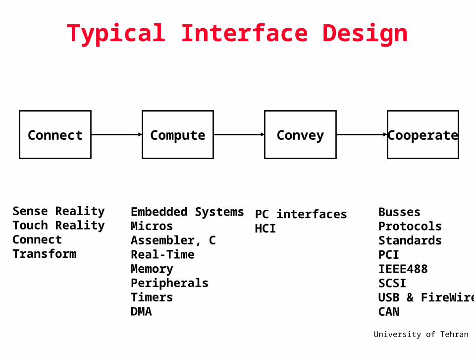
Typical Interface Design
Connect Compute Convey Cooperate
Sense RealityTouch RealityConnectTransform
Embedded SystemsMicrosAssembler, CReal-TimeMemoryPeripheralsTimersDMA
PC interfacesHCI
BussesProtocolsStandardsPCIIEEE488SCSIUSB & FireWireCAN
University of Tehran 4
University of Tehran 5
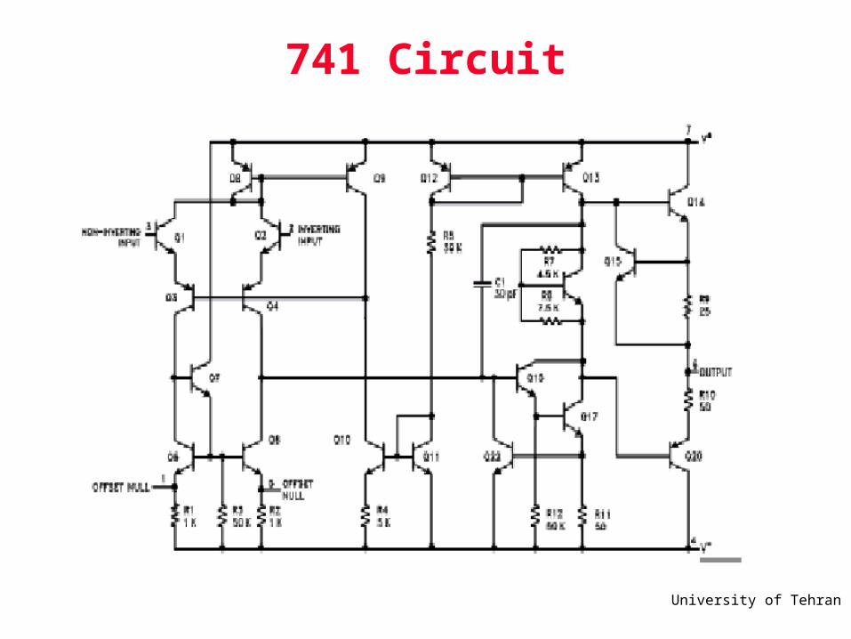
741 Circuit
University of Tehran 6
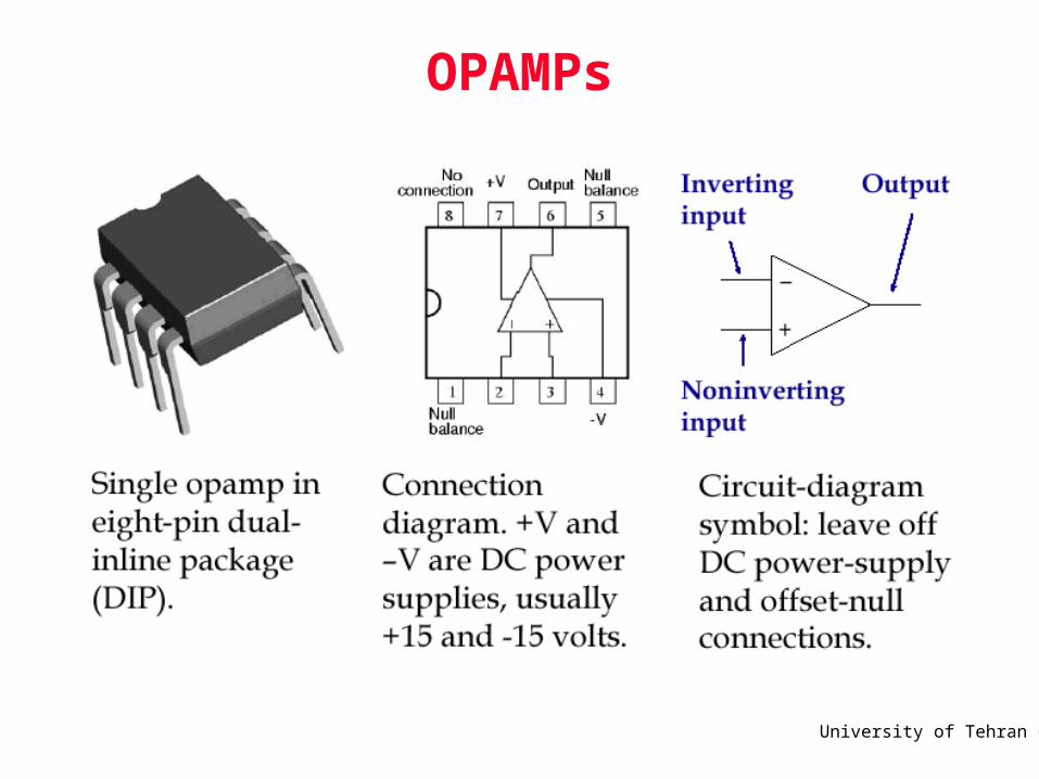
OPAMPs
University of Tehran 7
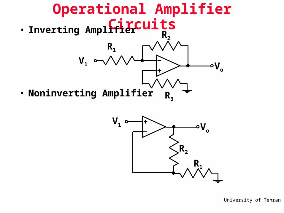
Operational Amplifier Circuits• Inverting Amplifier
• Noninverting Amplifier
V1 Vo
R1
R2
R3
V1
R1
R2
Vo
University of Tehran 8
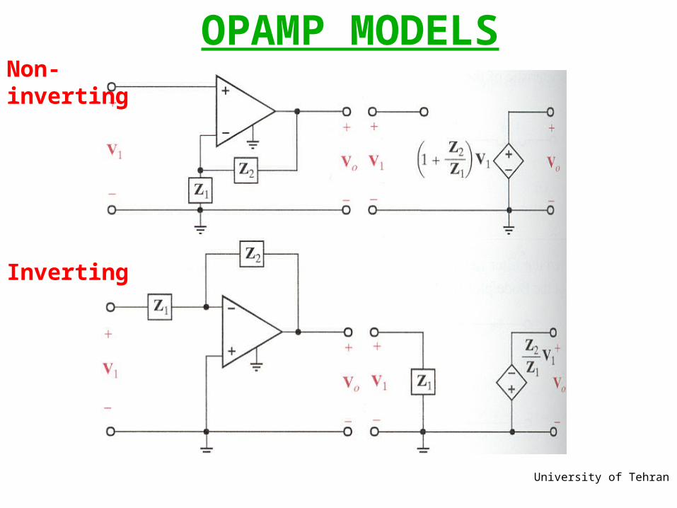
OPAMP MODELSNon-inverting
Inverting
University of Tehran 9
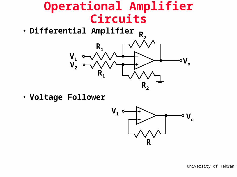
Operational Amplifier Circuits
• Differential Amplifier
• Voltage Follower
Vo
V1
R
Vo
V1
R1
R2
R2
V2R1
University of Tehran 10
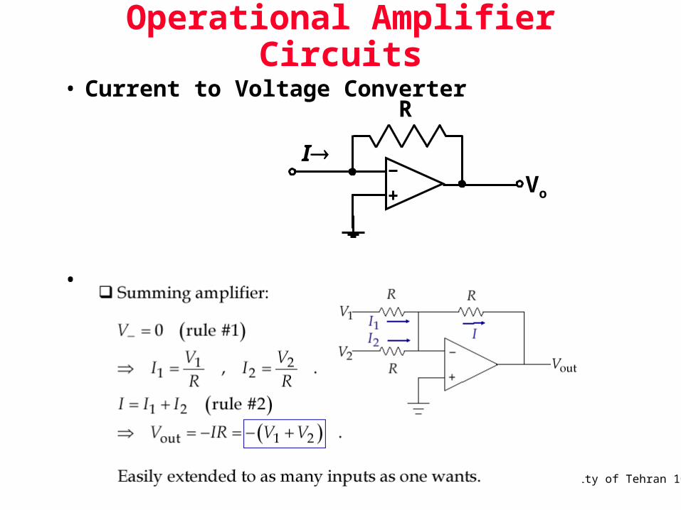
Operational Amplifier Circuits
• Current to Voltage Converter
• Summing Amplifier
R
IVo
VoV2
R2
R
V3
R3
V1
R1
University of Tehran 11
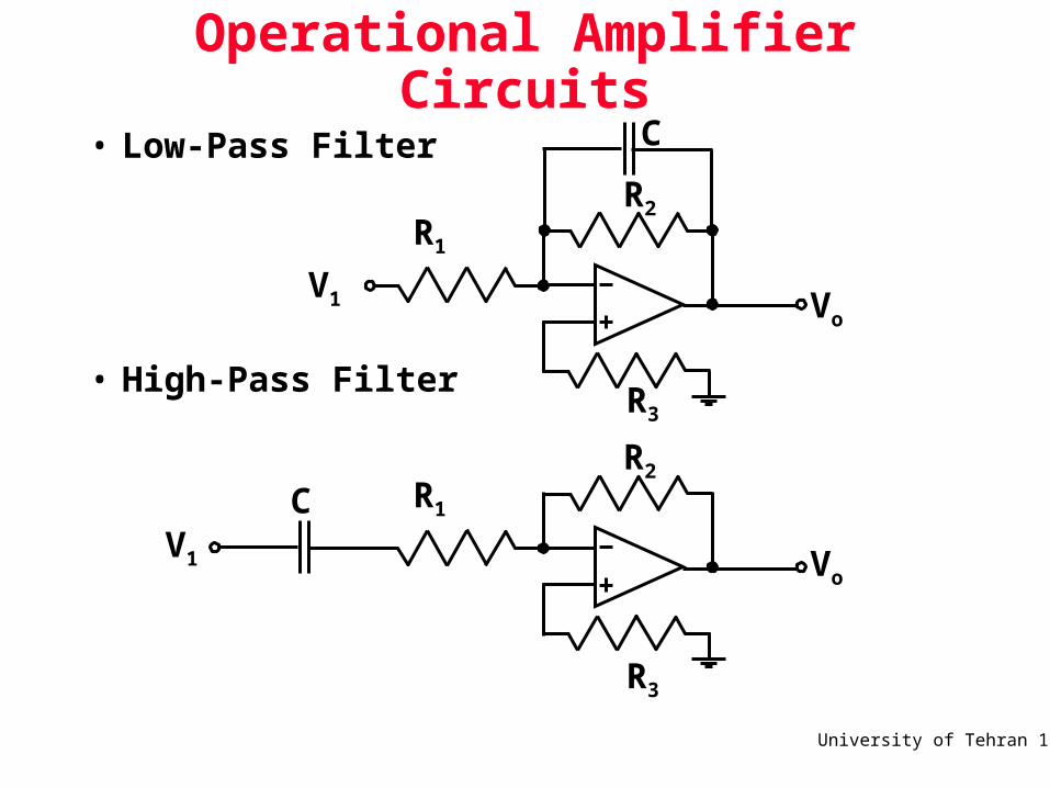
Operational Amplifier Circuits
• Low-Pass Filter
• High-Pass Filter
V1 Vo
R1
R2
R3
C
R2
V1 Vo
R1
R3
C
University of Tehran 12
Operational Amplifier Circuits
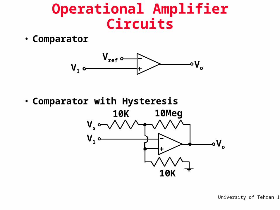
• Comparator
• Comparator with Hysteresis
V1Vo
Vref
10Meg
Vo
10K
10K
V1
Vs
University of Tehran 13
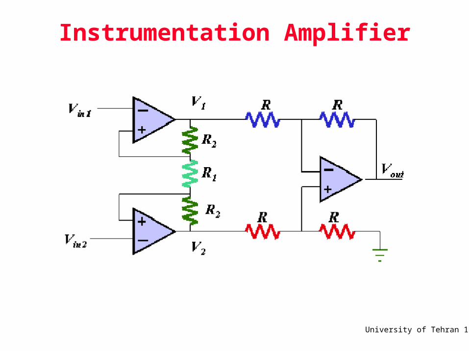
Instrumentation Amplifier
University of Tehran 14
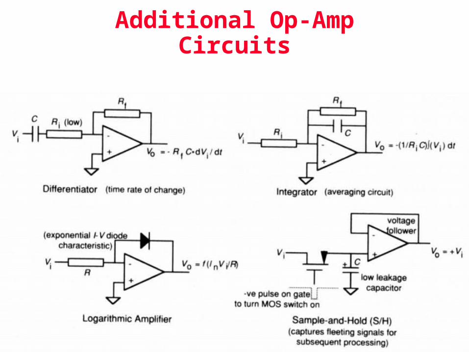
Additional Op-Amp Circuits
University of Tehran 15
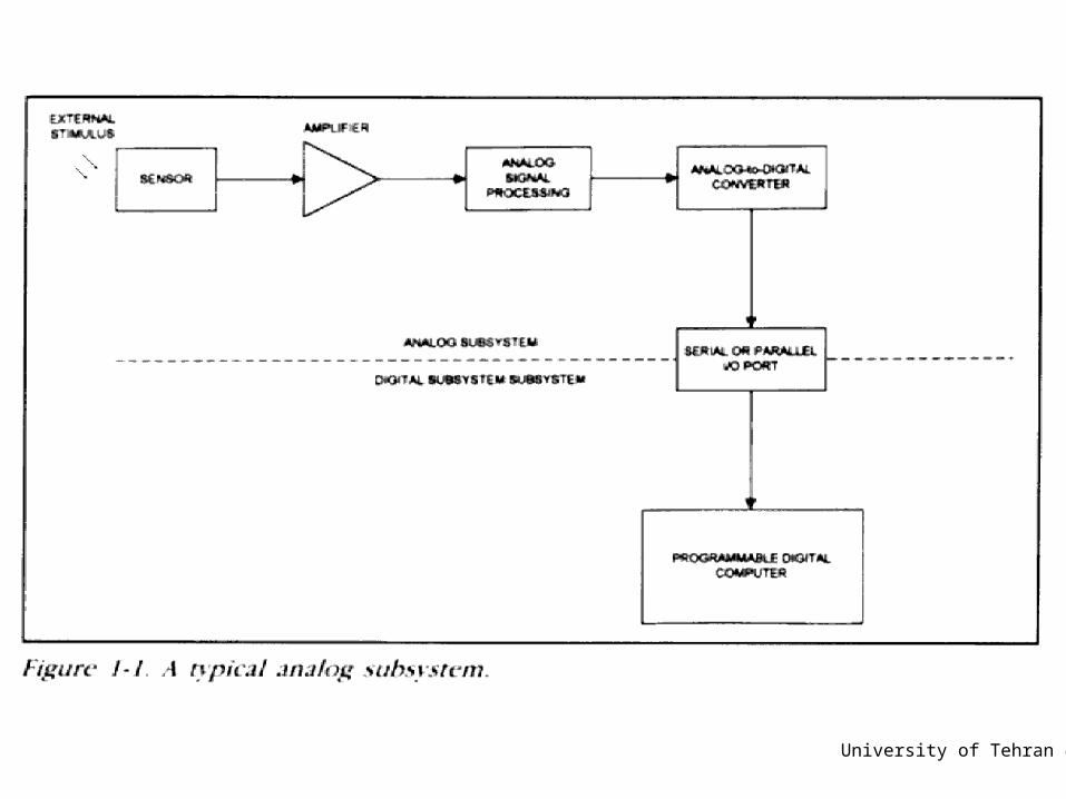
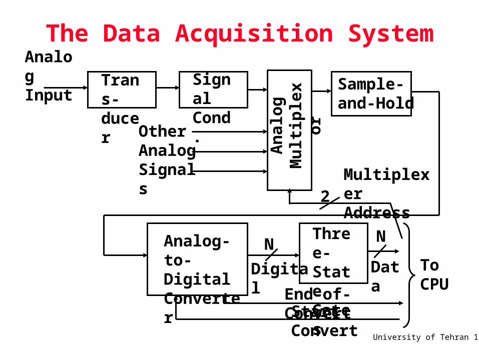
The Data Acquisition System
Trans-ducer
Analog Input Signal
Cond.
An
alog
Mu
ltip
lexo
r Sample-and-Hold
OtherAnalogSignals Multiplexer
Address2
Analog-to-DigitalConverter
N
Digital
Three-StateGates
N
Data ToCPU
End-of-ConvertStart Convert
University of Tehran 16
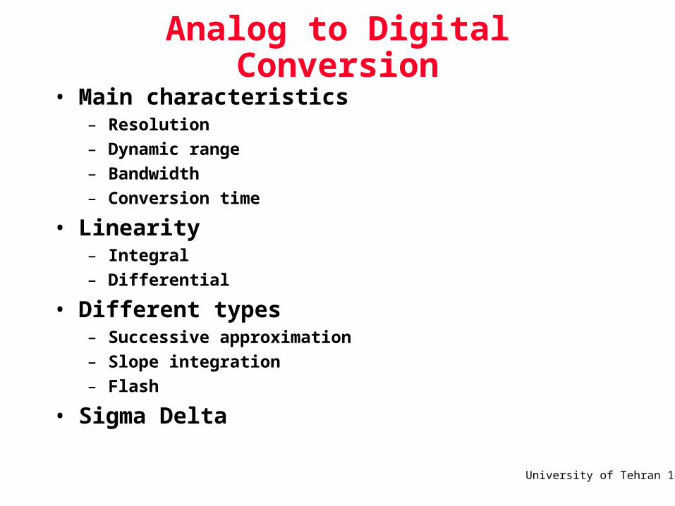
Analog to Digital Conversion• Main characteristics
– Resolution
– Dynamic range
– Bandwidth
– Conversion time
• Linearity– Integral
– Differential
• Different types– Successive approximation
– Slope integration
– Flash
• Sigma Delta
University of Tehran 17
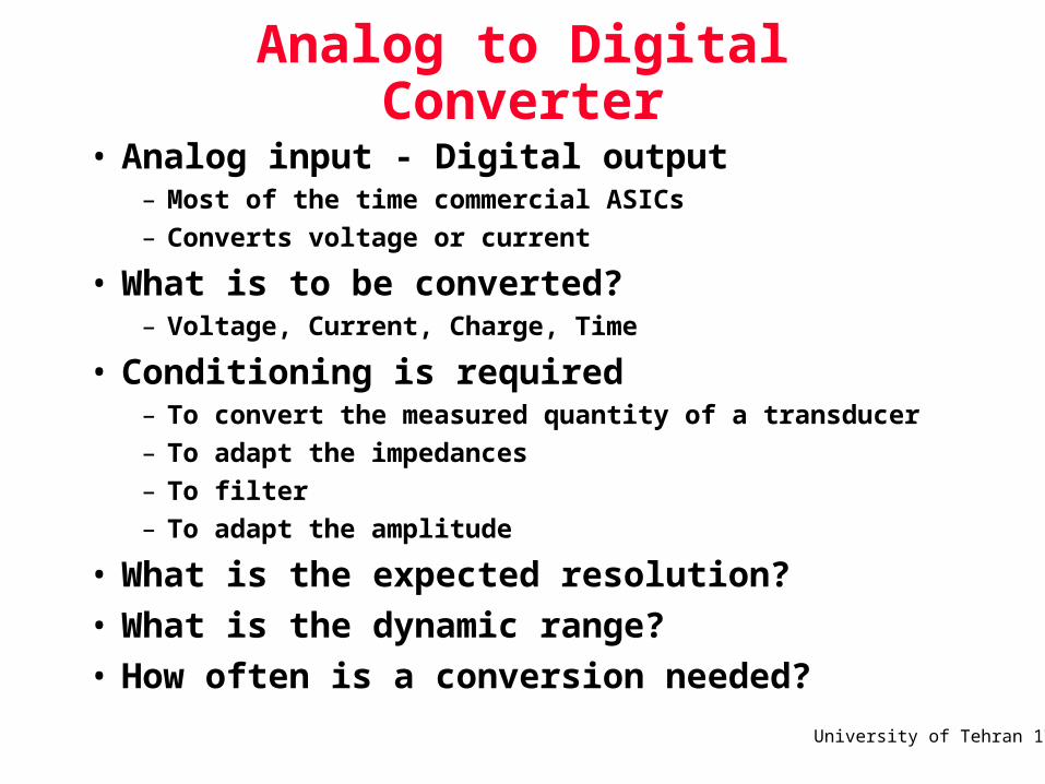
Analog to Digital Converter
• Analog input - Digital output– Most of the time commercial ASICs
– Converts voltage or current
• What is to be converted?– Voltage, Current, Charge, Time
• Conditioning is required– To convert the measured quantity of a transducer
– To adapt the impedances
– To filter
– To adapt the amplitude
• What is the expected resolution?
• What is the dynamic range?
• How often is a conversion needed?
University of Tehran 18
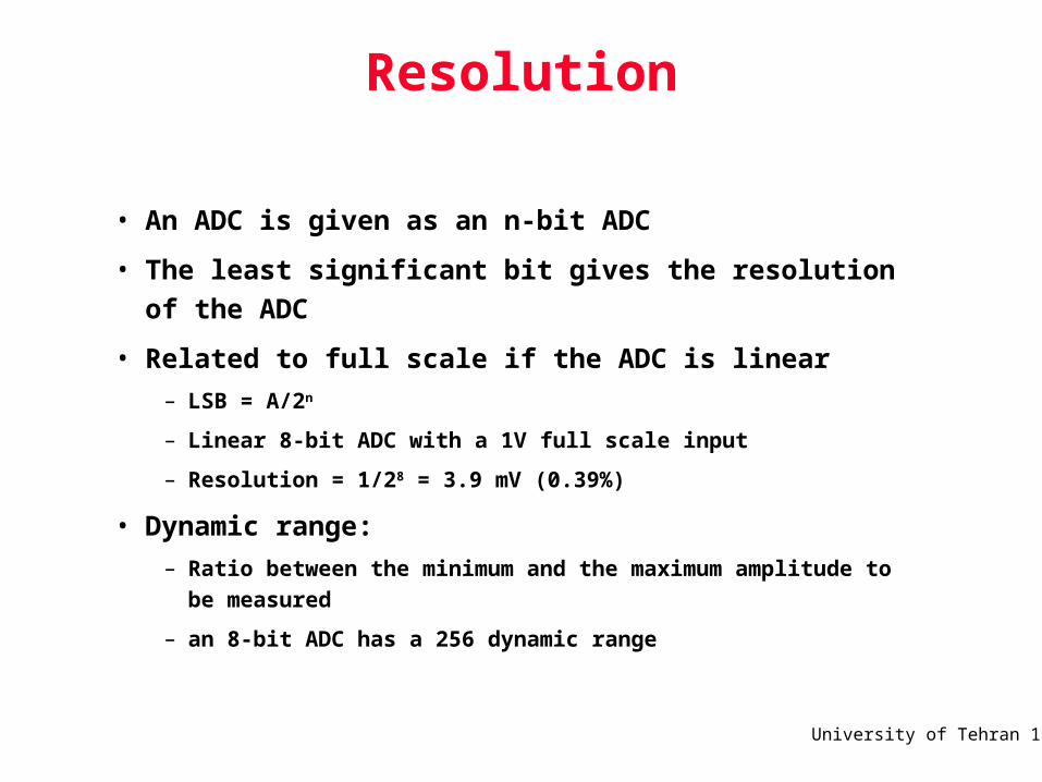
Resolution
• An ADC is given as an n-bit ADC
• The least significant bit gives the resolution of the ADC
• Related to full scale if the ADC is linear
– LSB = A/2n
– Linear 8-bit ADC with a 1V full scale input
– Resolution = 1/28 = 3.9 mV (0.39%)
• Dynamic range:
– Ratio between the minimum and the maximum amplitude to be
measured
– an 8-bit ADC has a 256 dynamic range
University of Tehran 19
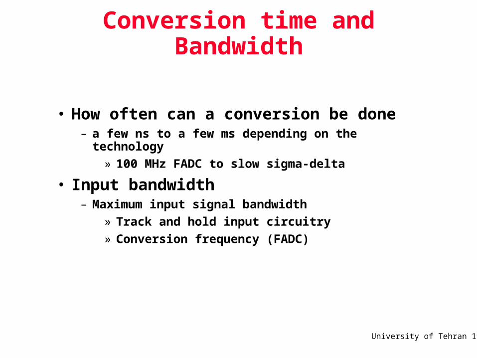
Conversion time and Bandwidth
• How often can a conversion be done– a few ns to a few ms depending on the technology
» 100 MHz FADC to slow sigma-delta
• Input bandwidth– Maximum input signal bandwidth
» Track and hold input circuitry
» Conversion frequency (FADC)
University of Tehran 20
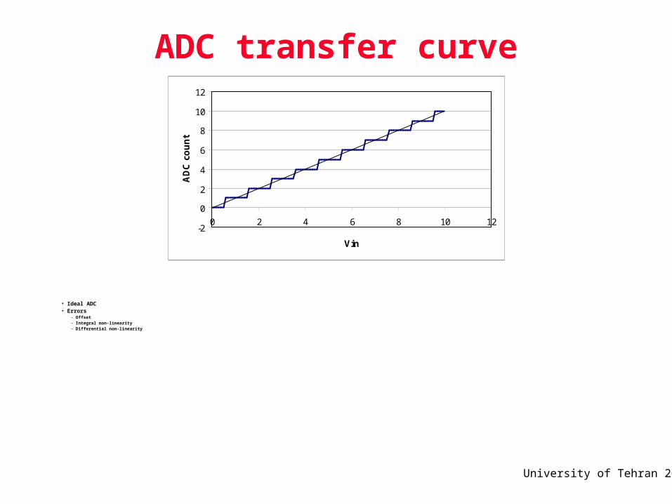
ADC transfer curve
• Ideal ADC• Errors
– Offset – Integral non-linearity– Differential non-linearity
-2
0
2
4
6
8
10
12
0 2 4 6 8 10 12
Vin
AD
C c
ou
nt
University of Tehran 21
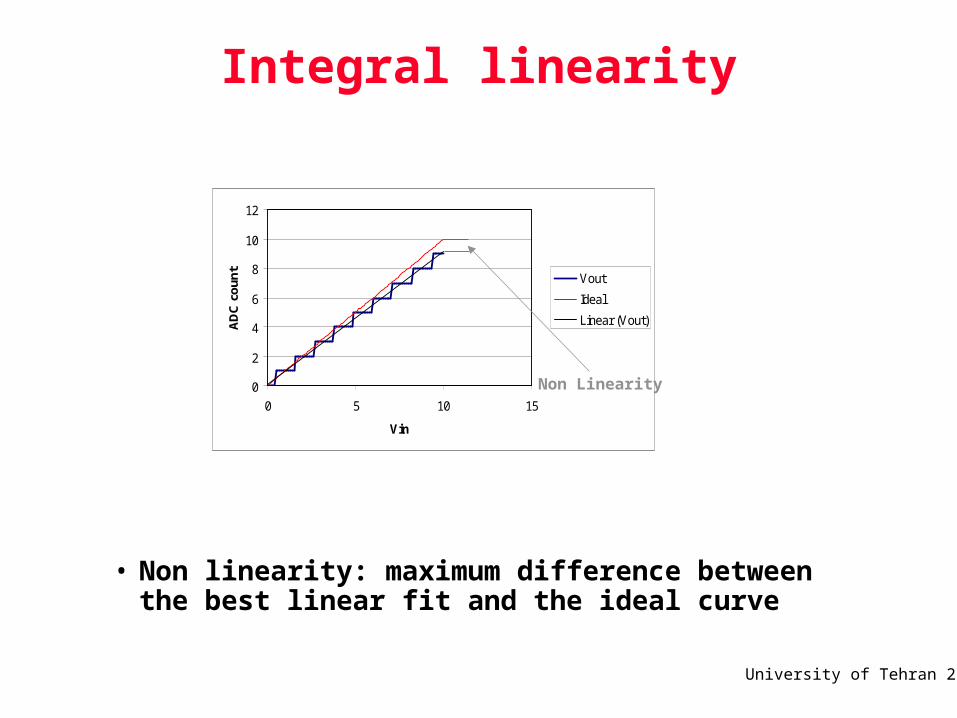
Integral linearity
• Non linearity: maximum difference between the best linear fit and the ideal curve
0
2
4
6
8
10
12
0 5 10 15
Vin
AD
C c
ou
nt
Vout
Ideal
Linear (Vout)
Non Linearity
University of Tehran 22
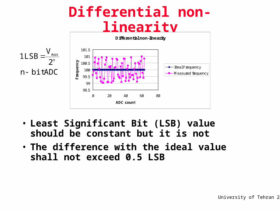
Differential non-linearity
• Least Significant Bit (LSB) value should be constant but it is not
• The difference with the ideal value shall not exceed 0.5 LSB
Differential non-linearity
98.5
99
99.5
100
100.5
101
101.5
0 20 40 60 80
ADC count
Fre
qu
en
cy
Ideal Frequency
Measured frequencyADCbitn2
V LSB 1
n
max
University of Tehran 23
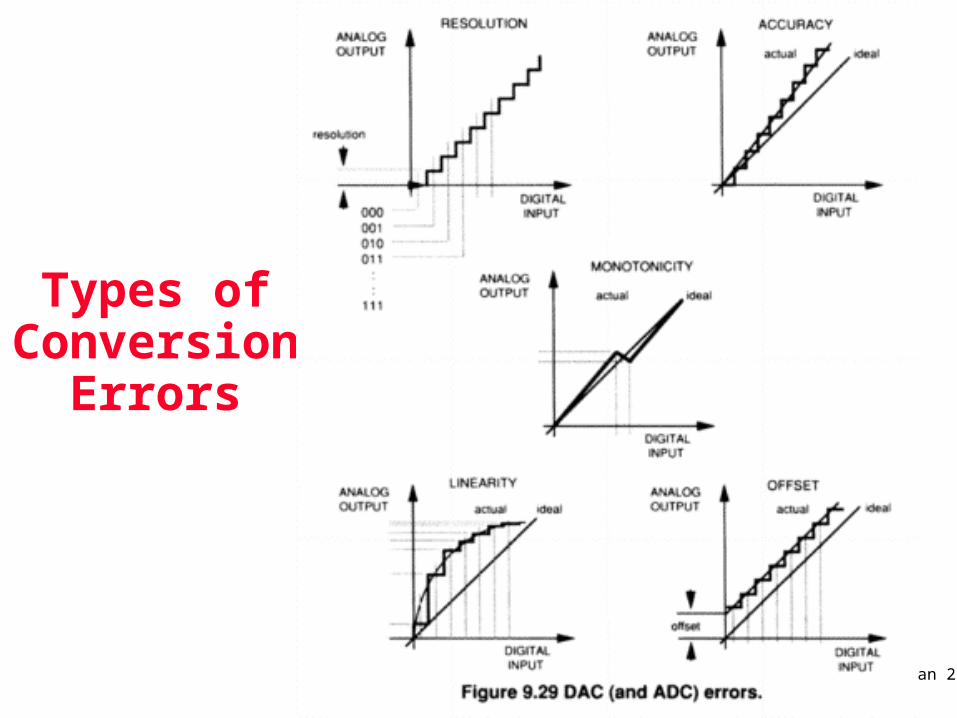
Types of Conversion
Errors
University of Tehran 24
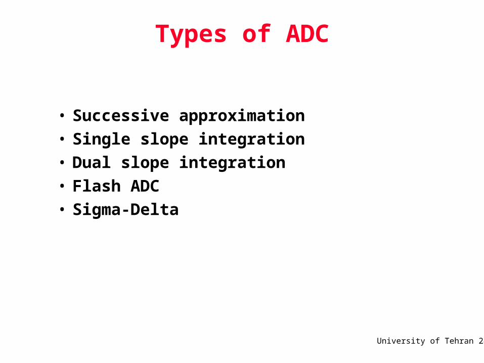
Types of ADC
• Successive approximation
• Single slope integration
• Dual slope integration
• Flash ADC
• Sigma-Delta
University of Tehran 25
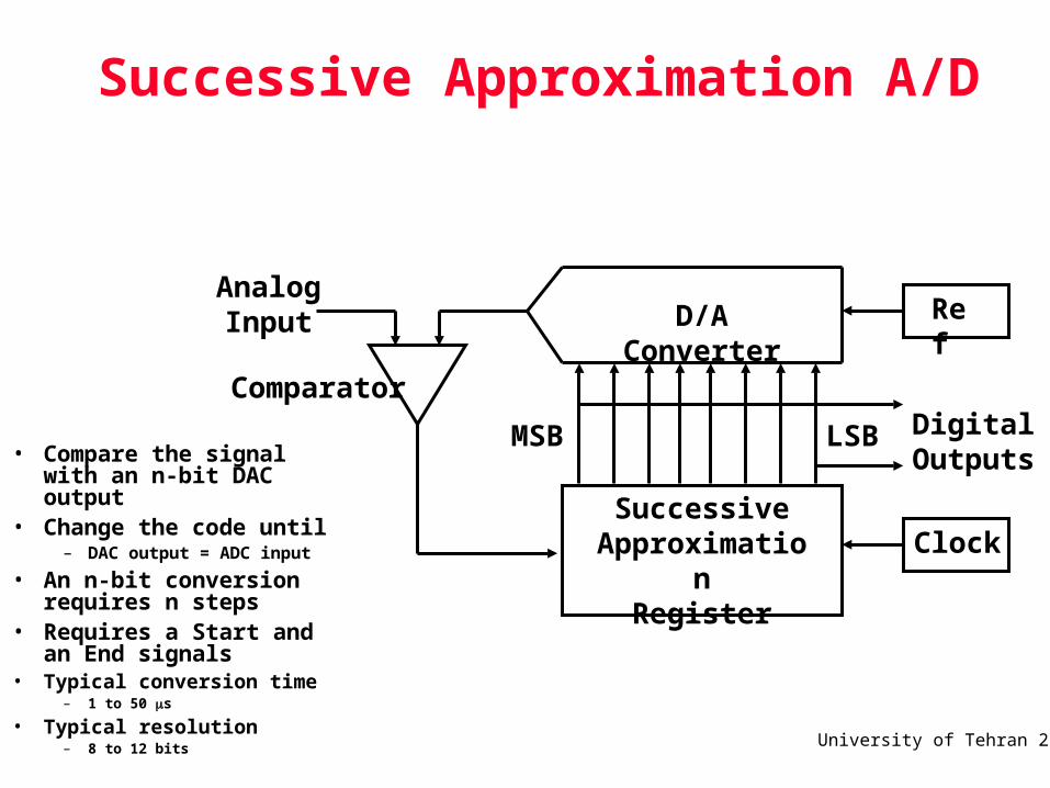
Successive Approximation A/D
• Compare the signal with an n-bit DAC output
• Change the code until – DAC output = ADC input
• An n-bit conversion requires n steps
• Requires a Start and an End signals
• Typical conversion time– 1 to 50 s
• Typical resolution– 8 to 12 bits
MSB LSB
D/A Converter
SuccessiveApproximation
Register
Ref
Clock
AnalogInput
ComparatorDigitalOutputs
University of Tehran 26
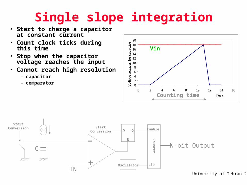
Single slope integration• Start to charge a capacitor at
constant current • Count clock ticks during this time• Stop when the capacitor voltage
reaches the input• Cannot reach high resolution
– capacitor– comparator
-
+IN
C
R
S Enable
N-bit Output
Q
Oscillator Clk
Co
un
ter
StartConversion
StartConversion
02468
101214161820
0 2 4 6 8 10 12 14 16
Time
Vo
lta
ge
acc
ross
th
e c
ap
aci
tor
Vin
Counting time
University of Tehran 27
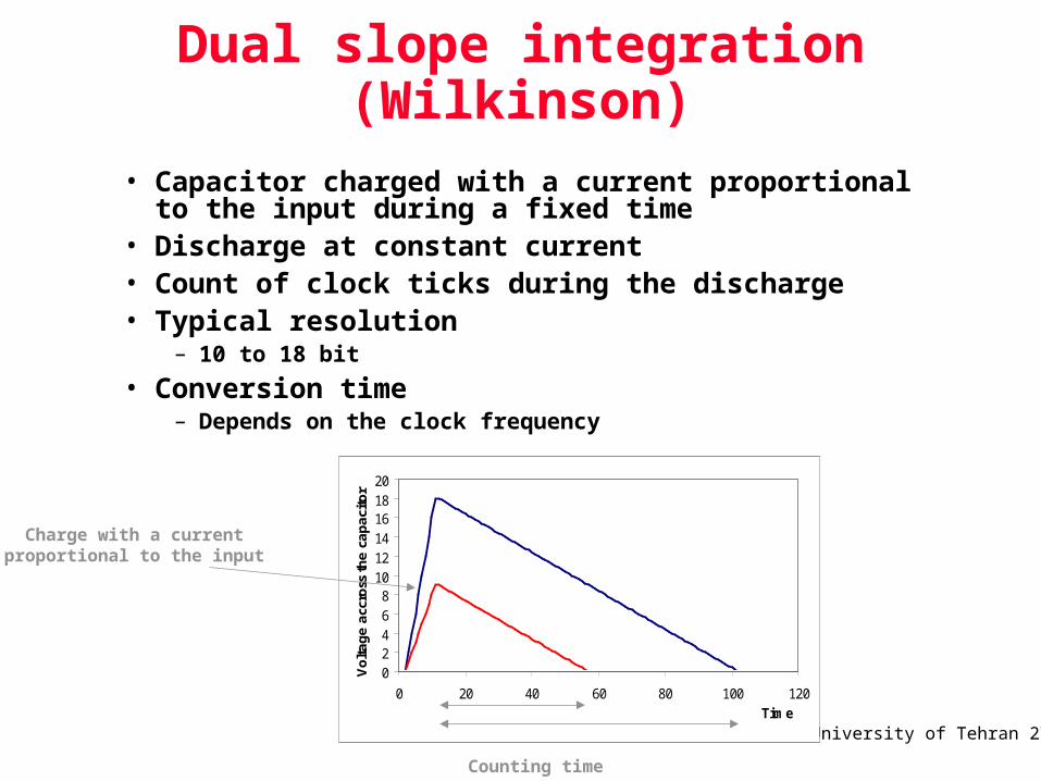
Dual slope integration (Wilkinson)
• Capacitor charged with a current proportional to the input during a fixed time
• Discharge at constant current• Count of clock ticks during the discharge• Typical resolution
– 10 to 18 bit
• Conversion time– Depends on the clock frequency
02468
101214161820
0 20 40 60 80 100 120Time
Vo
lta
ge
acc
ross
th
e c
ap
aci
tor
Counting time
Charge with a currentproportional to the input
University of Tehran 28
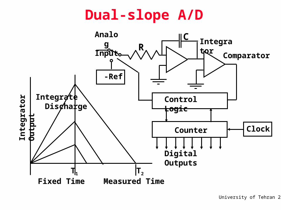
Dual-slope A/DIn
tegr
ator
Ou
tpu
t
T1 T2
Fixed Time Measured Time
Integrate Discharge
Counter
-Ref
Clock
AnalogInput
Comparator
Digital Outputs
IntegratorC
Control Logic
R
University of Tehran 29
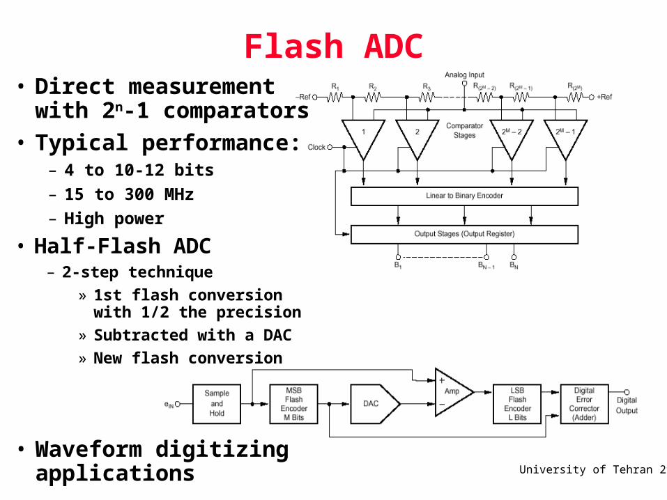
Flash ADC• Direct measurement with
2n-1 comparators
• Typical performance:– 4 to 10-12 bits
– 15 to 300 MHz
– High power
• Half-Flash ADC– 2-step technique
» 1st flash conversion with 1/2 the precision
» Subtracted with a DAC
» New flash conversion
• Waveform digitizing applications
University of Tehran 30
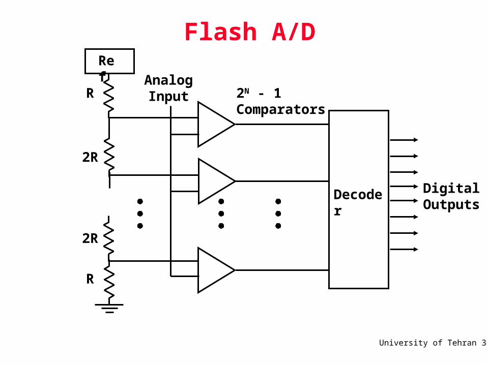
Flash A/DRef
AnalogInput 2N - 1
Comparators
DigitalOutputs
Decoder
R
2R
2R
R
University of Tehran 31
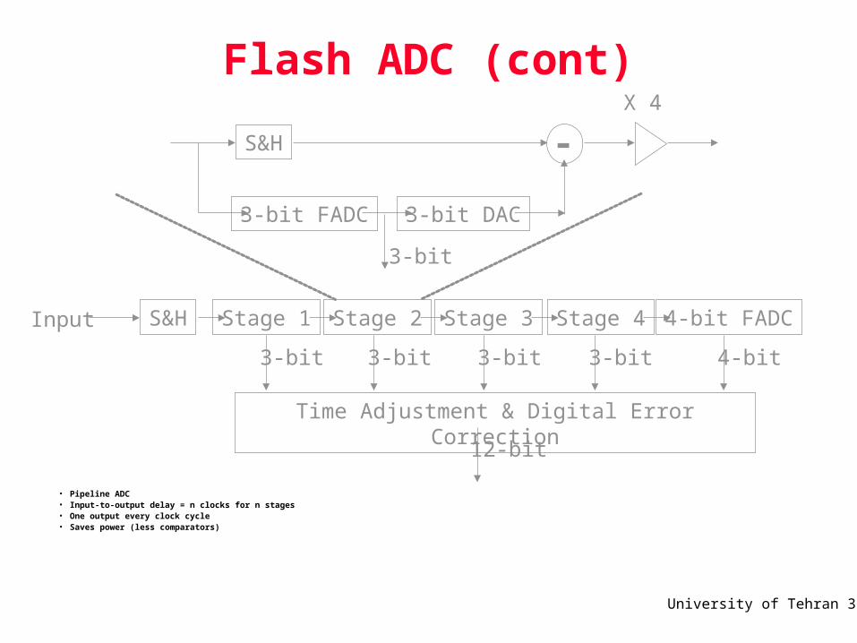
Flash ADC (cont)
• Pipeline ADC• Input-to-output delay = n clocks for n stages• One output every clock cycle• Saves power (less comparators)
S&H
3-bit FADC 3-bit DAC
-X 4
3-bit
S&H Stage 1 Stage 2 Stage 3 Stage 4 4-bit FADC
Time Adjustment & Digital Error Correction
3-bit 3-bit 3-bit 3-bit 4-bit
12-bit
Input
University of Tehran 32
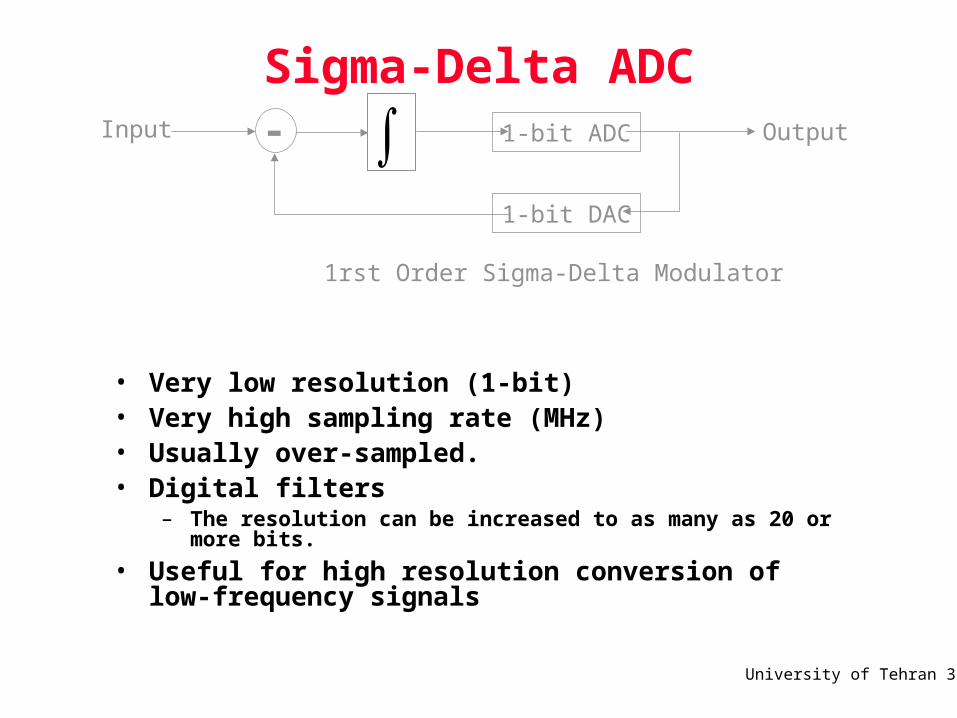
Sigma-Delta ADC
• Very low resolution (1-bit)• Very high sampling rate (MHz)• Usually over-sampled.• Digital filters
– The resolution can be increased to as many as 20 or more bits.
• Useful for high resolution conversion of low-frequency signals
1-bit ADC
1-bit DAC
-Input Output
1rst Order Sigma-Delta Modulator
University of Tehran 33
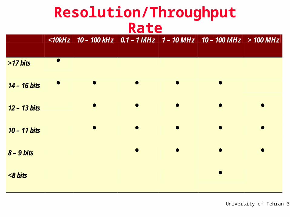
Resolution/Throughput Rate <10kHz 10 – 100 kHz 0.1 – 1 MHz 1 – 10 MHz 10 – 100 MHz > 100 MHz
>17 bits
14 – 16 bits
12 – 13 bits
10 – 11 bits
8 – 9 bits
<8 bits
University of Tehran 34
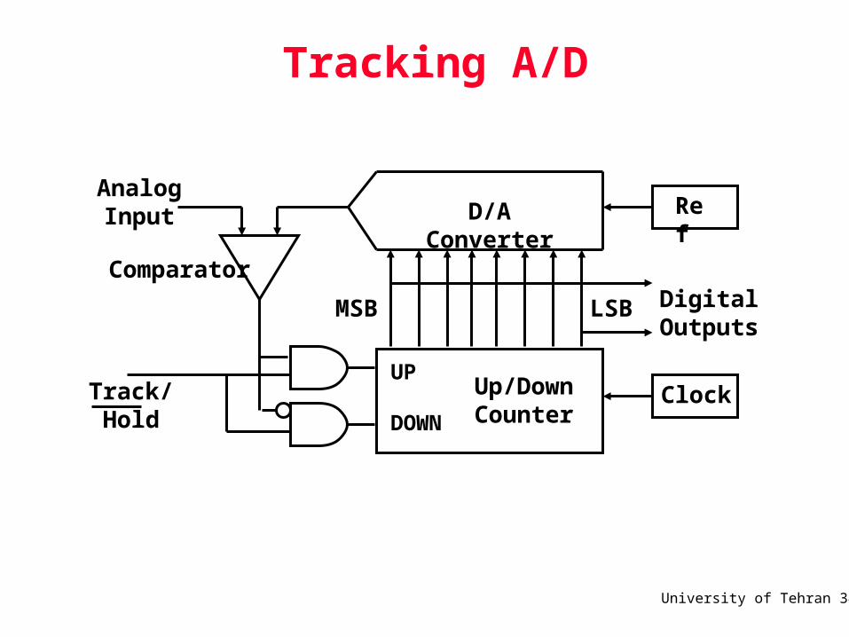
Tracking A/D
MSB LSB
D/A Converter
Up/DownCounter
Ref
Clock
AnalogInput
ComparatorDigitalOutputs
UP
DOWN
Track/ Hold
University of Tehran 35
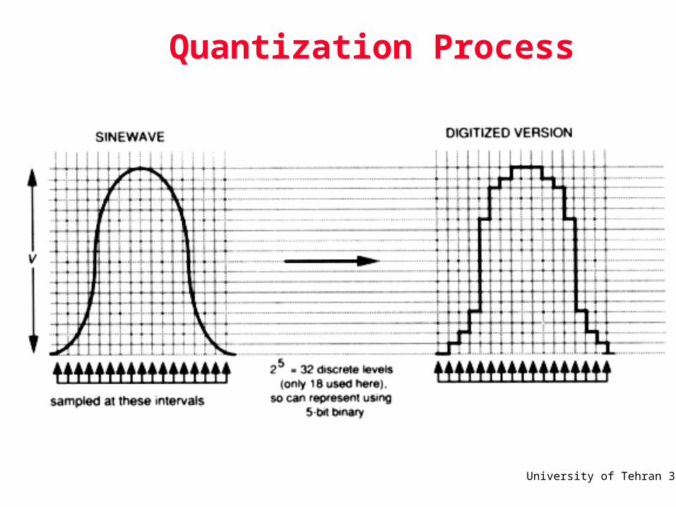
Quantization Process
University of Tehran 36
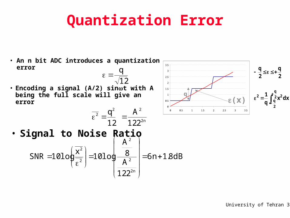
Quantization Error
0
0.5
1
1.5
2
2.5
3
3.5
0 0.5 1 1.5 2 2.5 3 3.5
(x)q
dxxq
1
2
q
2
q
2
q
2
q22
12
q
• An n bit ADC introduces a quantization error
• Encoding a signal (A/2) sint with A being the full scale will give an error
n2
222
212
A
12
q
dB8.1n6
212
A8
A
log10x
log10SNR
n2
2
2
2
2
• Signal to Noise Ratio
University of Tehran 37
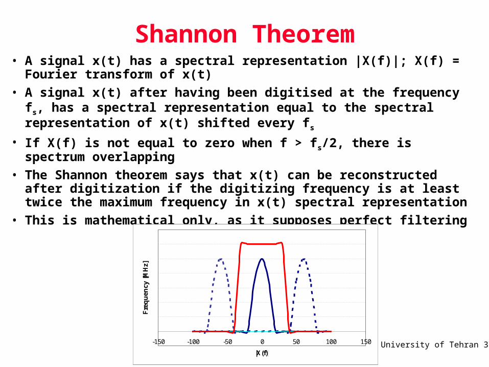
Shannon Theorem• A signal x(t) has a spectral representation |X(f)|; X(f) = Fourier
transform of x(t)
• A signal x(t) after having been digitised at the frequency fs, has a spectral representation equal to the spectral representation of x(t) shifted every fs
• If X(f) is not equal to zero when f > fs/2, there is spectrum overlapping
• The Shannon theorem says that x(t) can be reconstructed after digitization if the digitizing frequency is at least twice the maximum frequency in x(t) spectral representation
• This is mathematical only, as it supposes perfect filtering
-150 -100 -50 0 50 100 150
|X(f)|
Fre
qu
ency
[M
Hz]
University of Tehran 38
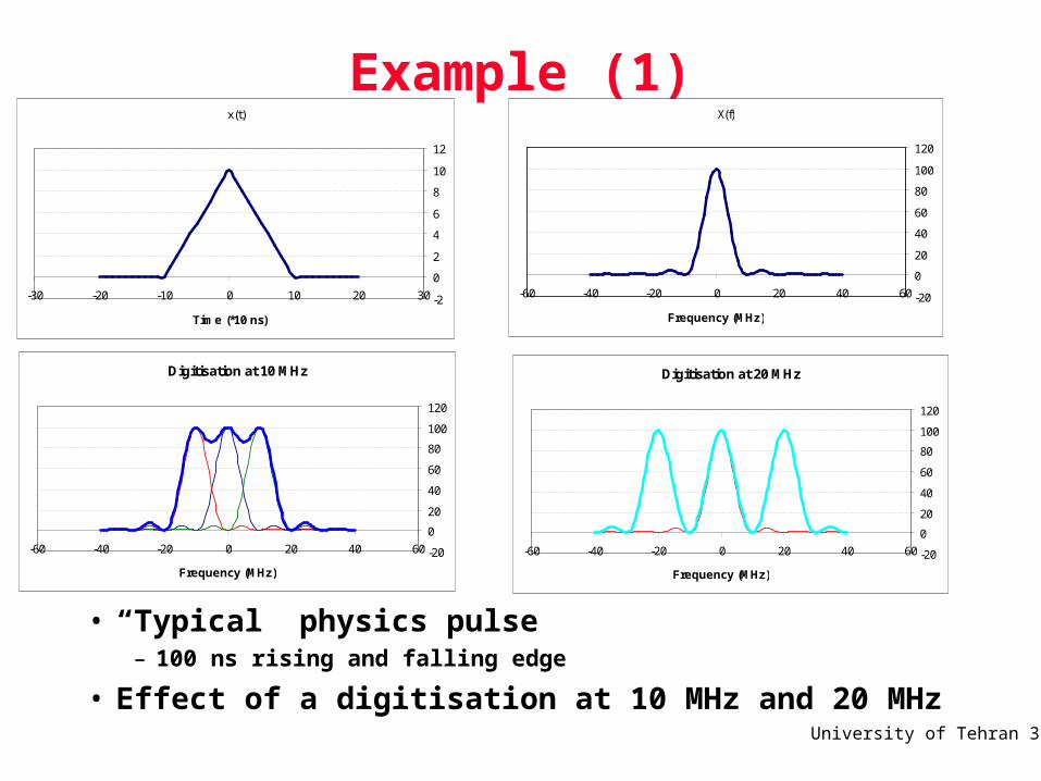
Example (1)
• “Typical” physics pulse– 100 ns rising and falling edge
• Effect of a digitisation at 10 MHz and 20 MHz
X(f)
-20
0
20
40
60
80
100
120
-60 -40 -20 0 20 40 60
Frequency (MHz)
x(t)
-2
0
2
4
6
8
10
12
-30 -20 -10 0 10 20 30
Time (*10 ns)
Digitisation at 10 MHz
-20
0
20
40
60
80
100
120
-60 -40 -20 0 20 40 60
Frequency (MHz)
Digitisation at 20 MHz
-20
0
20
40
60
80
100
120
-60 -40 -20 0 20 40 60
Frequency (MHz)
University of Tehran 39
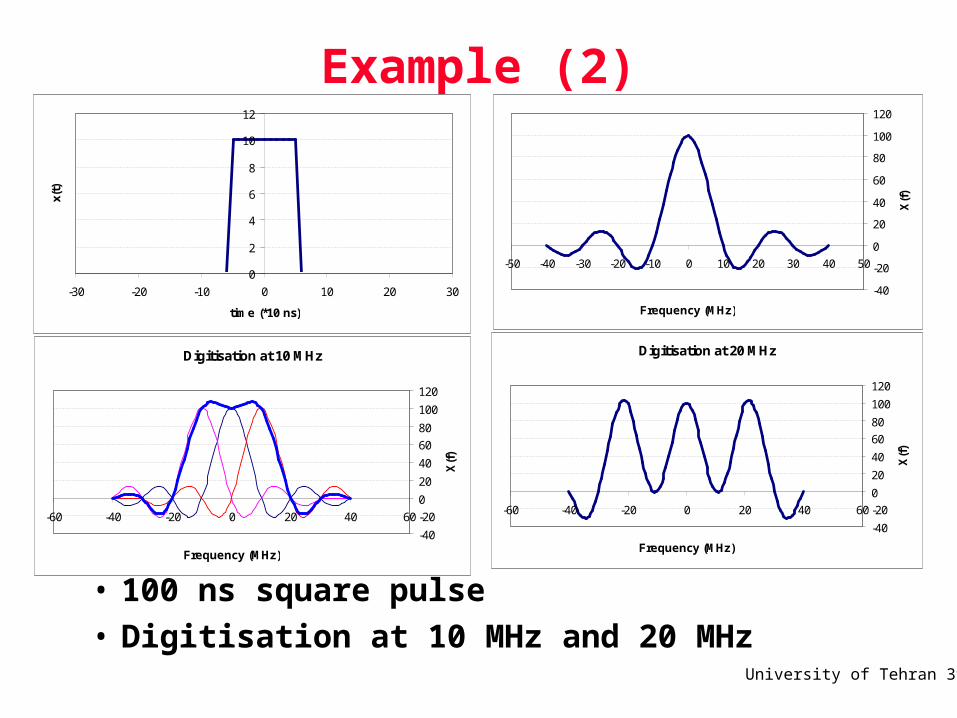
Example (2)
• 100 ns square pulse
• Digitisation at 10 MHz and 20 MHz
0
2
4
6
8
10
12
-30 -20 -10 0 10 20 30
time (*10 ns)
x(t)
-40
-20
0
20
40
60
80
100
120
-50 -40 -30 -20 -10 0 10 20 30 40 50
Frequency (MHz)
X(f
)
Digitisation at 10 MHz
-40
-20
0
20
40
60
80
100
120
-60 -40 -20 0 20 40 60
Frequency (MHz)
X(f
)
Digitisation at 20 MHz
-40
-20
0
20
40
60
80
100
120
-60 -40 -20 0 20 40 60
Frequency (MHz)
X(f
)
University of Tehran 40
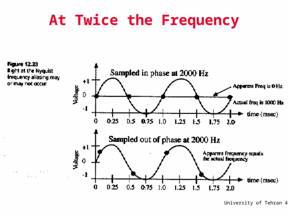
At Twice the Frequency
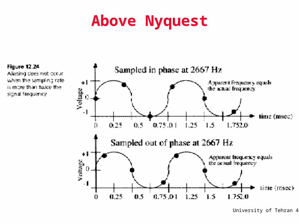
University of Tehran 41
Above Nyquest
University of Tehran 42
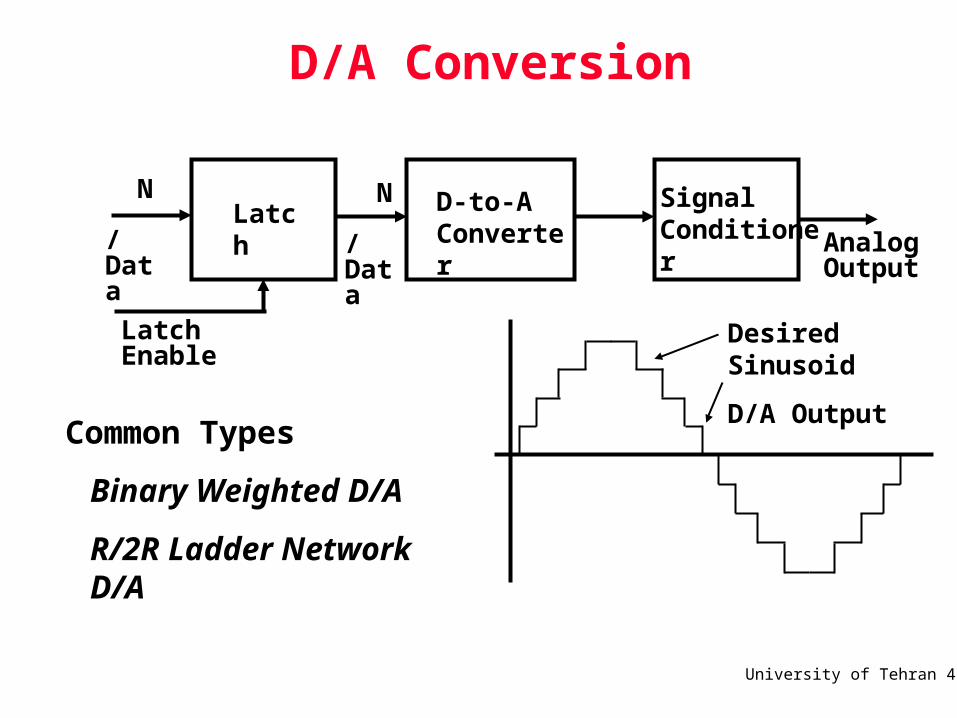
D/A Conversion
Desired Sinusoid
D/A Output
N /Data
Latch N /Data
D-to-AConverter
SignalConditioner Analog
Output
LatchEnable
Common Types
Binary Weighted D/A
R/2R Ladder Network D/A
University of Tehran 43
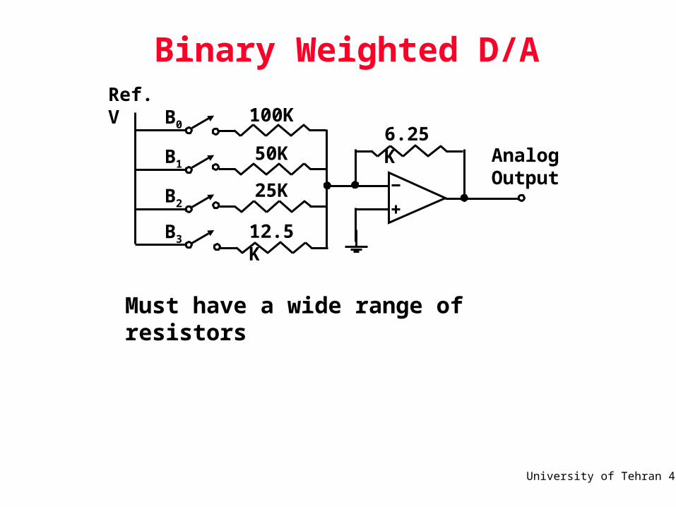
Binary Weighted D/A
AnalogOutput
B0
B1
B2
B3
Ref. V100K
50K
25K
12.5K
6.25K
Must have a wide range of resistors
University of Tehran 44
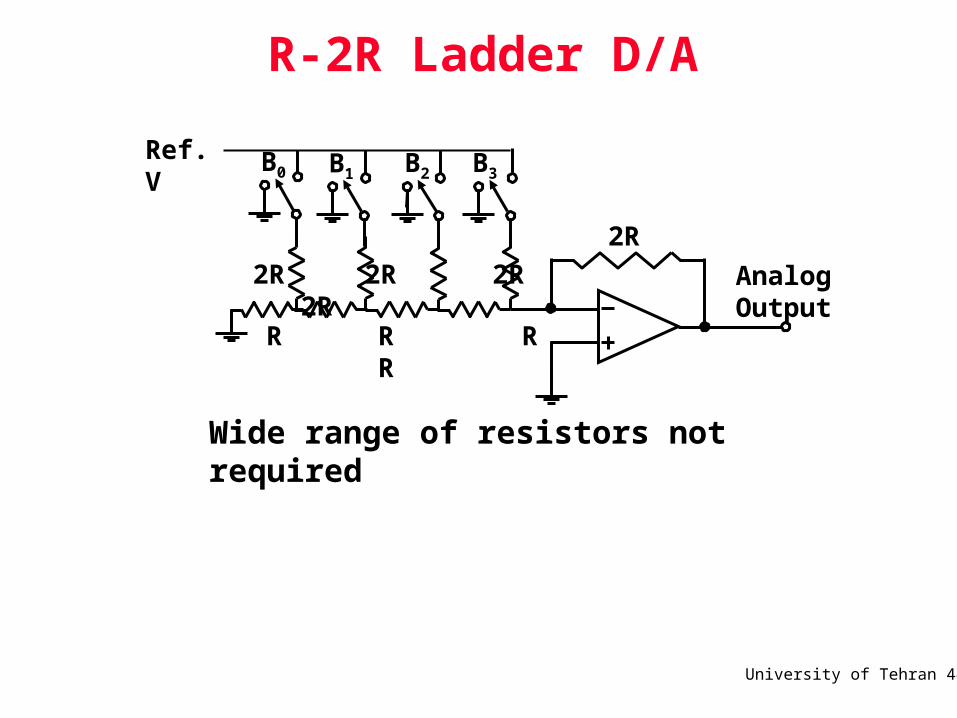
R-2R Ladder D/A
AnalogOutput
B0 B1 B2 B3Ref. V
2R
2R 2R 2R 2R
R R R R
Wide range of resistors not required
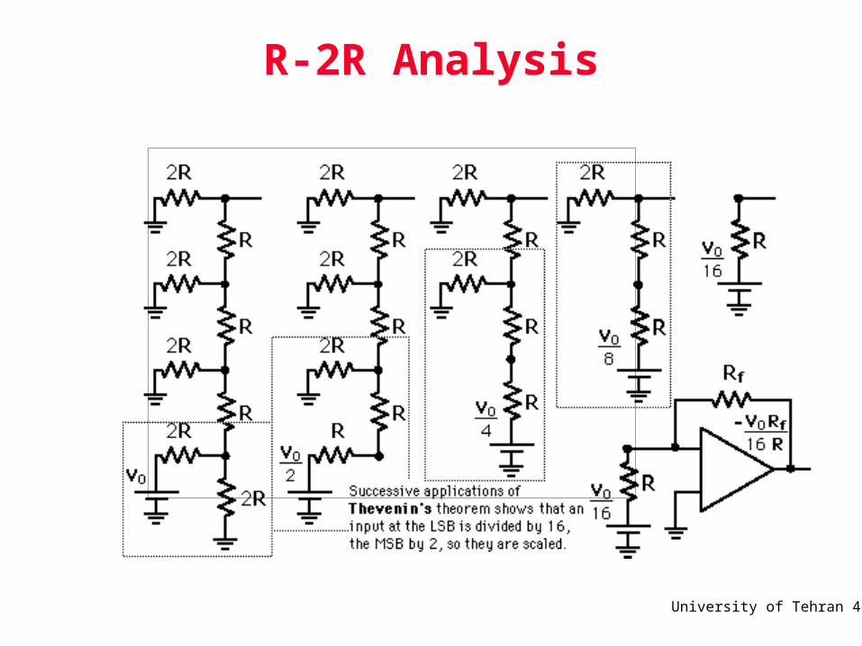
University of Tehran 45
R-2R Analysis
University of Tehran 46
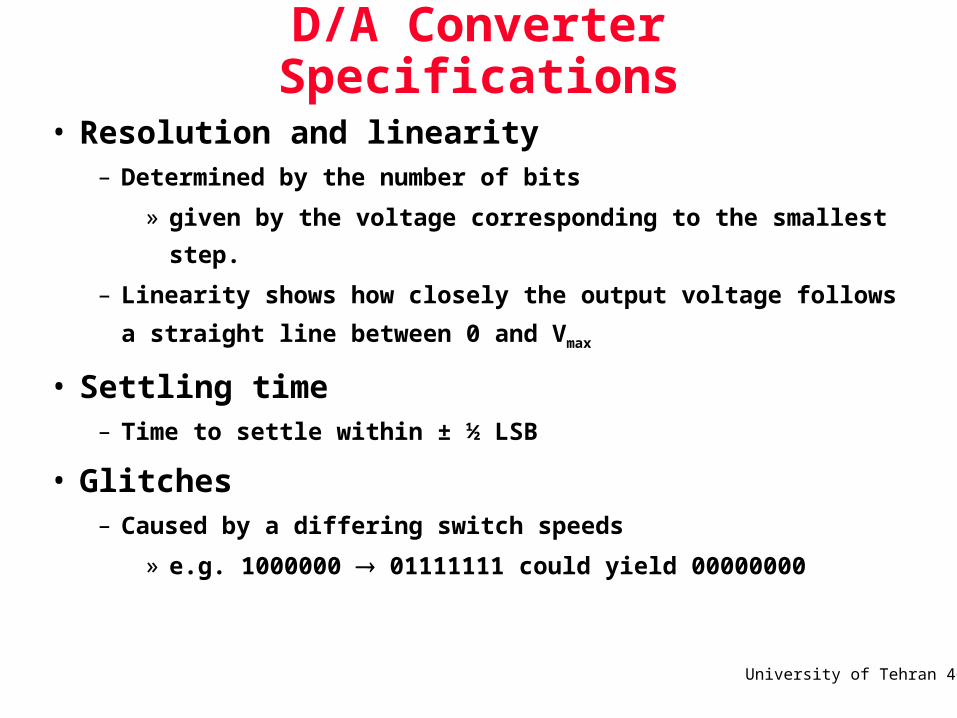
D/A Converter Specifications
• Resolution and linearity– Determined by the number of bits
» given by the voltage corresponding to the smallest step.
– Linearity shows how closely the output voltage follows a straight
line between 0 and Vmax
• Settling time– Time to settle within ± ½ LSB
• Glitches– Caused by a differing switch speeds
» e.g. 1000000 01111111 could yield 00000000
University of Tehran 48
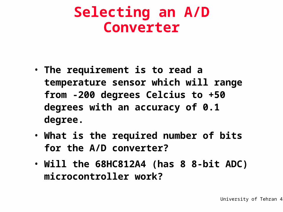
Selecting an A/D Converter
• The requirement is to read a temperature sensor which will range from -200 degrees Celcius to +50 degrees with an accuracy of 0.1 degree.
• What is the required number of bits for the A/D converter?
• Will the 68HC812A4 (has 8 8-bit ADC) microcontroller work?
University of Tehran 49
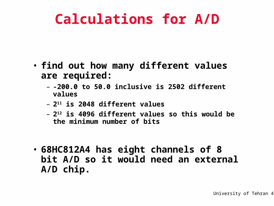
Calculations for A/D
• find out how many different values are required:
– -200.0 to 50.0 inclusive is 2502 different values
– 211 is 2048 different values
– 212 is 4096 different values so this would be the minimum number of bits
• 68HC812A4 has eight channels of 8 bit A/D so it would need an external A/D chip.
University of Tehran 50
Summary
• OP-AMPs
• OP Amp circuits
• Analog to digital converters
• Quantization
• Sampling frequency
• Digital to analog converters