univ edinburgh (scotland) dept of smiith … i iiterials(u) heriot-biatt univ edinburgh (scotland)...
TRANSCRIPT

"RD-A14.9 551 OPTICA~LLY BISTRBLE DEVICES USING SEMIICONDUCTOR /I IITERIALS(U) HERIOT-bIATT UNIV EDINBURGH (SCOTLAND) DEPTI OF PHYSICS S D SMIITH ET AL. NOV 84 RAlDC-TR-84-229UNCLASSIFIE FOSR-82-8i49F/6 9/ NL
EllllnlllllllEl.'...llll

o" -7; L I- S . . .
13.
13.
lIiiOOP 1.0 OLUTI TES CHAR5
NAT1 I .25 URA OF11 1.A4P 196 1.

RADC-TR-84-229Final Technical ReportNovember 1984 4
OPTICALL Y BISTABLE DEVICES USINGe SEMICONDUCTOR MATERIALS
I-Lfl
* 0) Heriot-Watt University
S. D. Smith DTICa M. E. Prise S ELECTE
C. T. Seaton JAN25F. A. P. Tooley N 2 5C. R. Pidgeon
APPROVED FOR PUBLIC RELEASE" DISTRIBUTION UNLIMITED
'-I
ROME AIR DEVELOPMENT CENTERAir Force Systems Command
Griffiss Air Force Base, NY 13441.5700
85 0 12S

This report has been reviewed by the RADC Public Affairs Office (PA) andis releasable to the National Technical Information Service (NTIS). At NTISit will be releasable to the general public, including foreign nations.
RADC-TR-84-229 has been reviewed and is approved for publication.
APPROVED: J vCHARLES L. WOODSProject Engineer
APPROVED:
HAROLD ROTH, DirectorSolid State Sciences Division
FOR THE COMANDER: QJOHN A. RITZActing Chief, Plans Office
o
If your address has changed or if you wish to be removed from the RADC mailinglist, or if the addressee is no longer employed by your organization, pleasenotify RADC (ESO) Hanscom AFB MA 01731. This will assist us in maintaining acurrent mailing list.
* Do not return copies of this report unless contractual obligations or noticeson a specific document requires that it be returned.
•

REPORT DOCUMENTATION PAGEI& REPORT SECURITY~ CLASSIFICATION lb. RESTRICTIVE MARKINGe
UNCLASS IFIED N/A2&. sacUarlTy CLASSIFICATION AUTHORITY 3. OISTRIBUTIONAVAILABILITY OF REPORT
X/A Approved for public release; distribution2b. OCCLASSIFICATION/OOWNGMAOING SCHEDULE unlimited.V/A ____________________
a PERFORMING ORGANIZATION REPORT NUMBER(S) S. MONITORING ORGANIZATION REPORT NUMBER(S)
N/A RADlC-TR-84-229
Ga. NAME OF PERFORMING ORGANIZATION EBb. OFFICE SYMBOL 7a. NAME OF MONITORING ORGANIZATION
Heriot-Watt University jRome Air Development Center (ESO)
6c. ADDRESS (City. State and ZIP Code) 7b. ADDRESS (City. State and ZIP Code)
Chambers Street Hanscom AFB MA 01731Edinburgh, U.K.
Ba. NAME OF FUNOgNG/SPONSORIING 8b. OFFICE SYMBOL 9. PROCUREMENT INSTRUMENT IDENTIFICATION NUMBERORGANIZATION if apie~
AFOSR ESO AFOSR-82-0149
B. ADDRESS lCity. Stae and ZIP Code) 10. SOURCE OF FUNDING NOS.
PROGRAM PROjECT TASK IWORK t.NIT
Boln F C232ELEMENT NO. NO. NO. NO.
It T TLE lnedae Security Csa.fcasw61 0 F 3 6 24
OPTICALLY BISTABLE DEVICES USING SEMICONDUCTOR MATERIALS12. PSON01AL AUTHOR IS)
S. D. Smith, M. E. Prise, C. T. Seaton, F. A. P. Tooley, C. R. Pidgeon
ThFial Bistbiliy an deic properte 8 f INohvembeen 1984 tcaed O34 ai
by. 30ATCE IsplesaSaeln .0 SUBJEC withM eCnries of esei nJ, s- andeonstedy by usingumer
heL design an oSuctono an. aonletned Optical Sermcondctorsiie conssigol2hu0 ibt cytlpme by Bsabit 30pIusnfo e YG ae a ee civo
20. OSRBTOtVIAIIYO ~RC 2 ABSTRACT SECURITYi CLASSIFICATION ad detfybyblc nmbr
ThiLs rportE ovUIers SAME ASdute RPTm FeTuar US9RS Co ~ C SFIeray18 nh olna
22tca N roeMie Of RemSPONSIctoE usingOA tunable TELEPONE NUMeRoat lase OFEsMoLes
Emphass is o CO laer stdies o In~b t 77K bud a, od.clpaaerimliirichasres e for Woodsoko ssesatsote aelnts
Th Otca Bsabliyan dvceprprteso ________________ _ (617) 861 en2 i tr~atDC (EOeato
LNCLASS IFIED
SECURITY CLASSI PICATION OP iWIS PAGI
This system utilizing a grating feedback arrangement provides picosecond (pulse) tunable
radiation from 1.45 to 2.111.m. Optical absorption saturation, above the band edge ofIn0 .5 3Ga0 .4 7As is being studied using this system.
UNCLLSSIFIEDSGCUMITY CLASSIPICAflON OP TMea PA'Z
DEPARTMENT OF PHYSICS
HERIOT-WATT UNIVERSITY
Edinburgh, U.K.(Tel: 031-449 5111)
Air Force Office of Scientific Research
Research Proposal: Optically Bistable Devices using Semiconductor Materials
Final Report on Grant No. AFOSR-82-0149
Principal Investigator: Professor S. D. Smith FRS
Accession For
NTIS cF:A,j4 D2'IC TV:i
Cino. -7
DTICJAN 25 1985 2'.
B 4.

4 -1 -
PART 1
1 SUMMARY'
The operation of a natural reflectivity InSb bistable resonator
at 77 K pumped with a cw CO laser at 1819 an- , as a single pulse detector
with a definite threshold energy (5 nJ), and as an optical AND gate is
reported. The switching pulses are provided by a modelocked Nd:YAG laser,
operating at 1.06 urm (9430 an- ) producing single 35 ps pulses. A unique
technique is used in which two 1.06 urn, 35 ps pulses separated by a variable
time delay are used to measure the photogenerated carrier lifetime. A
recombination time of 90 ns has been measured for a cw holding intensity
of 80 W/cm2 .
2 Introduction
Several recent reviews have been written on optical bistability and
related phenomena covering both experimental and theoretical work. For
a more general account of the topic the reader is referred to them
A brief qualitative explanation of dispersive bistability is given here.I
This is followed by details of the construction and operation of an InSb
bistable element. The switching mechanisms of this device are discussed
and the concept of "external" switching introduced. Our experimental
results are then presented and the implications of these results reviewed,
both in terms of the non-linear refractive effects in InSb and more generally
as the operation of an all-optical logic element.
It is important to note the potential significance of this work.
Despite the many publications soeculating on the uses of this refractive
• . . - . - . . . . .', . . ' . - - . . ,. . . - . .

-2-
effect in different III-V semiconductors, and other similar low power
electronic non-linear refractive effects in semiconductors such as that
observed in GaAs by Gibbs et al the InSb/CO laser system is the only
such device which has shown bistability using a cw laser. Therefore it
offers a unique opportunity to observe and study the behaviour of such a
system, under various conditions, notably from the steady state to dynamic
switching on picosecond timescales.
The work presented in this chapter has been the subject of two
conference papers(5)(6) and an Applied Physics Letter (7 )
3 Dispersive Optical Bistability
The simplest dispersive optical bistable device is a Fabry-Perot
resonator filled with a medium in which the refractive index is dependent
on the optical field intensity.
The condition for maximum transmission in a Fabry-Perot resonator is
that the length of the resonator is equal to an integral number half
wavelengths of the incident light. In the non-linear case this can be
written as
"-- n(I)Zl 2
where m is an integer, Z is the cavity length and \ is the wavelength.
The function n(I) expresses the dependence of refractive index on intensi:z,
which to first order can be taken as
n(I) = n0 + n2 1
4 -3-
If the cavity is held slightly of f resonance, then by varying the incident
intensity it is possibly to move towards resonance. Figure 1 shows
the typical transmission characteristics of a Fabry-Perot resonator, as
a function of frequency. The shape of the curve depends on the finesse
of the cavity. An increase in intensity has the effect of moving this
curve to the left if the refractive index reduces with intensity as is
the case in InSb, under the experimental conditions used here. As the
cavity moves towards resonance, a greater proportion of the incident
light is allowed into the cavity, therefore the non-linear effect increases
with effective positive feedback. This mechanism allows small signal gain.
At higher intensities the transmission will drop again, as the cavity is
moved off resonance, and at even higher intensities the next resonance will
occur, and a series of steps of increasing and decreasing transmission will
occur.
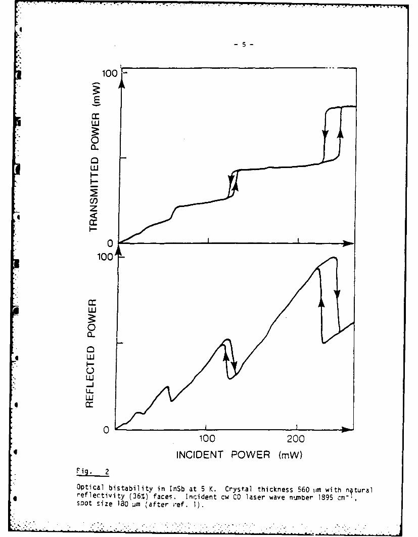
Figure 2 shows the input power versus output power for an InSb
cavity at a wavelength and intensity for which the refractive index is
intensity dependent, and the transmission steps can be seen. When the
change in transmission induced by a change in incident intensity is large
enough, enough intensity is allowed into the cavity to make the transmission
change so rapidl'y that an instability can result, and the cavity can be pulled
onto resonance into a stable state. A similar effect occurs as the inout
intensity is decreased and the device switches itself from off to on
resonance. The region of input powers where two stable states exist is
known as the bistable region.
A rigorous mathematical account of what is happening has proved very
hard to formnulate and many approaches have been used. Felber and Marburger (8 )

-4
CC
C C000
U, U)4) 4)
C 4
0 0'
-. *---- A4!sua4ui Pa4JI .SuOjj
Fig. 1
transmission characteristics of a Fibry Perot resonator.
-5-
100 '
E
LU
0a.
LU
CC,
0100
LU
0a.
* LU
LU-
100 200* INCIDENT POWER (mW)
Optical bistability in InSb at 5 K. Crystal thickness 560 pm with n~tural4 reflectivity (36%) faces. Incident cw CO laser wave nmber 1895 cm--,0 SPOt size 180 wn rafter ref. 1).

S- 6 -
* simply extended the plane wave theory for a linear non-absorptive
Fabry-Perot interferometer. These results qualitatively predict what
is observed. In the real situation in InSb and in other materials, sane
absorption is required to create the refractive index change, and Gaussian
laser beams are used rather than infinite plane waves.
O.A.B. Miller(9) examined the situation using a plane wave theory
and incorporating linear absorption. He deduced some interesting parameters
for optimising bistable devices. The most interesting from th -'int of
view of this thesis is that for a bistable device, the mos' O ortant
materials parameter for a low switching intensity is not the ",i of n ,
it is the magnitude of the ratio n2/z. So a weaker n2 can be counteracted
. by having a lower absorption coefficient. For a given cavity, with a mirror
reflectivity R, and absorption A, he found the minimum intensity for switching
occurred when I - R a A. Since A = exp (-ciL), where a is the linear absorotion
coefficient and L is the cavity length, a smaller n2 means a longer cavity is
required, requiring also a smaller absorption coefficient.
These results can be explained by considering that as the absorotion
coefficient increases the effective interaction length with the non-linear
material decreases. By balancing the absorption length, the cavity length
and the mirror reflectivities to provide the maximum interaction length
in the non-linear material, the lowest power bistability will occur.
Miller's results provide sane very useful guides to Possible new bistable
systems, but to completely describe the experimental observations the
Gaussian beam nature of the pumo beam must be taken into account ana tne
diffusion of photo-excited carriers included.
Several authors have tried to introduce a Gaussian pump beam into
the oroblem. The introduction of spatial variations in the beam profile
4- 7
results in the need for numerical solutions using enormous amounts of
computer time. The most relevant work to the effects observed in InSb
is that done by Firth and Wright (lO ) Their results have been applied
with some degree of success to experimental observations ( l). In particular
the form of the spatial hysteresis seen experimentally was predicted by
using their numerical model. Much theoretical work is going on into the
proper treatment of transverse soatial effects in bistable systems,
partially because of the interesting effects observable and partially
because of the great interest in using these devices for parallel image
*I processing.
One area in which very little work has been done is the inclusion of
carrier diffusion in the problem. Since the diffusion length in InSb is
several hundred microns, this is clearly going to be of some significance
when trying to construct several elements near to each other on one crystal.
There is still, therefore, a .ery large amount to be done on the InSb
bistable system, before a complete understanding is obtained.
I 4 InSb Optically Bistable Resonator
The experimental layout used to set up the bistable resonator was
the same as that used in previous experiment The
Fabry-Perot cavity consisted of a 210 um thick InSb crystal (n-type
4 x 1 cm" ) with natural reflectivity (R = 0.36) polished faces,
4 mounted in a rotatable cryostat, and held at a temperature of 77 K.
Radiation was provided by an Edinburgh Instruments PL3 cw CO laser onerating
I , i o ' - " " - ' . . " - . ."" " '

* - 8-
at 1819 cn 1 . The beam was focussed onto the sample using a BaF 2 lens
to produce an incident beam diameter of 200 pm. This was measured using
a pyroelectric detector with a 10 um pinhole, scanned across the beam.
Variation in intensity over 4 or 5 orders of magnitude while maintaining
the Gaussian beam profile was obtained using a variable attenuator slide
in conjunction with a spatial filter (13 ) The input and output powers
were monitored using Laser Precision cw power meters, the outputs of
which were connected to the x and y channels of a storage oscilloscope.
This system allows transmission measurements to be made very easily
and quickly over several orders of magnitude of incident intensity, and
has proved to be extremely useful in looking for non-linear optical
effects around the bandgap in InSb ( 14 ) . The sample was moved about in
the laser beam, its variation in thickness being used t3 get the correct
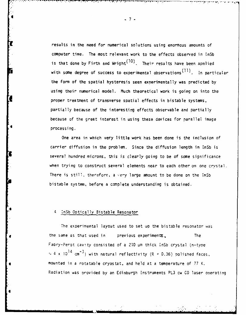
cavity detuning for optimum bistability (15 ). The input versus output
power is shown for this detuning (fig. 3). As can be seen for input
powers of around 25 mW two possible outputs are available for a given
input. This is known as the bistable region. The lower branch of the
curve is as previously discussed known as the off-resonance transmission
state, and the upper branch the on-resonance state.
Using samples with PbTelZnS high reflectivity mirrors, bistabilitv
has been obtained using much lower intensities, but a natural uncoated
sample was used here to make as simple a system as oossible.
S
0"
- 9 -
4
E
W
0 1"5
S1-0C',zI-
4 20 25 30[a] INCIDENT POWER [mW]
~T
E 1-5o z-: -'-- IN'
0
0
Nd.YAG1
.- * PULSE' timeFF
[b] ULj INTERRUPT tmCO SEAM
InSb Sa"plet-2 1OjjR-36%,
Laser on 1819cri
spot dia.-O.2mm
F'ig. 3(a) Transmitted power plotted, against icident power. 1b) Trancmlssionof incident rw CO laser "eam at . 26 mW showing "on" switching caused
*l by a single 35 ps pulsc from a %d:YAG laser. Switch off is caused byinterrupting the CO holding beai.
:: : .: , _ . : _ . - • . .. .. . . . -. . .. :. .

* -10-
5 Switching Oynamics
The use of this device as an optical memory is of great interest,
and hence the switching speed is of great importance. The mechanisms
involved in the switching are extremely complicated, due to the spatial
effects of defocussing on the Gaussian input beam, the coupling between
*the forward and the backward field, the time taken for the refractive
index change to follow the intensity change and carrier diffusion.
As has been stated previously - under the excitation
conditions used here refractive index change is directly proportional to
the number of photoexcited carriers. It is only in the steady state
condition that An = n21. For a change in refractive index to occur
excited carriers must be created or recombine. The change in optical
path length (Ant) required for switching can be estimated to be in the
experimental conditions used %, A/10 from the theory of Felber and Marburgerf 8 )
The time taken for refractive index to increase, i.e.carriers to decay
after an instantaneous change in intensityis obviously the excited
carrier recombination time, which is 100-1500 ns,
he amount of time taken for the refractive index to decrease i.e. carriers
to be excited after an instantaneous increase in intensity is more complicated.
This depends on the rate at which carriers can be excited, as well as on the photo-
excited carrier recombination rate.
* If all the carriers are created by a cw CO laser this time can be
quite long 50-500 ns. The switching process will be conside-ably complicated
by spatial and diffusion effects. The switch-up time can be decreased by
* using progressively higher laser powers including some means other than a
. CO laser to introduce the necessary photoexcited carriers. Similarly the
•
- 11 -
switch down time, dependent on the carrier recombination time, could be
changed by engineering the material, say using surface or defect effects
to reduce carrier lifetime.
The fundamental limit on switching is the cavity field build up time t
given by
2noL
tc Z 0 5.1c(l-R)
In the cavity used L = 210 pm, and R 0.36, so tc = 8 ps. This is the
fundamental limit on switching speed in this device.
The experiment described in the next sections provided some information
on the dynamics involved,
6 Switching of an InSb bistable resonator held with a cw 5.5 um
laser beam, using a 1.06 um 35 ps pulse
A Nd:YAG modelocked laser was used to produce a single short (35 os)
pulse, which was incident on the active area of the sample. The experimental
layout is given in figure 4.
The bistable cavity was set up so its transmission characteristic wasI
given by figure 3(a). The input Dower was adjusted so it was in the
off-resonance position, or lower branch of the bistable loop. The Nd:YAG
laser was turned on with a 1 Hz repetition rate: neutral density filters were
used to find out at what energy the cavity could be made to switch from off-
to on-resonance with a single pulse. By displaying the output from the
nower meter on an oscilloscope with a very slow time base, it could easilyI

WVW
121
CICC
<JL0 0
Pig 4 .L
CL Z - *.
- 13
be seen when a switch takes place. The cavity was reset by blocking the
incident beam and the next pulse 1 s later, switched it again.
Figure 3(b) shows this happening.
The threshold energy for switching was found to be 5 nJ, incident on
the active area of the sample. The exact energy was obtained by using a
5 ma radius Nd:YAG beam on the sample and working out how much was incident
on the 200 uzm I/e diameter of the cw CO holding beam, which forms the bistable
element. The energy measurements were done using a Laser Precision Rk 7000
pyroelectric energy meter. This was interfaced to an HP85 minicomputer for
easy data collection.
The mechanism for switching was obviously non-thermal, since an
increase in temperature would cause an increase in refractive index (since
at 77 K an increase in temperature of InSb results in a narrowing of the
bandgap) and this would not cause a switch from off to on to occur. The
1.06 vm pulse causes a decrease in refractive index and hence an increase
in transmission so more CO intensity is allowed into the cavity and this
holds the cavity on resonance, even when the effect of the pulse has
decayed away.
The mechanism responsible for the switch on is the creation of
electrons in the conduction band of the InSb sample by the Nd:YAG nulse.
These can be created by three mechanisms, either by excitation from the
split-off band which is 1.13 eV below the conduction band, by excitation
from the heavy hole high up into the conduction band or from the light hole
into the conduction band. These excited electrons only have a major effect
on the refractive index at the CO holding beam frequency if they occupy
states near the band edge. The electrons will thermalise rapidly down to
-14-
the bottom of the conduction band, before relaxing to the valence band.
The thermalisation process will occur in < 1 ns, perhaps < 100 ps, then
the electrons will take several hundred nanoseconds to relax back in to
the valence band.
The electrons, while at the bottom of the conduction band, cause the
refractive index to change sufficiently to change the optical path length
enough to increase the cavity transmission (for the 1819 an-1 holding beam)
to a level where the holding beam can itself maintain a high enough carrier
concentration, to keep the cavity on-resonance. The whole switching process
is complicated by a number of factors, notably the Nd:YAG oulse is absorbed
in the first I un of the sample, because of the high absorption coefficient.
" Diffusion must therefore be taken into account, as well as the interband
scattering, and the Gaussian beam nature of the holding beam.
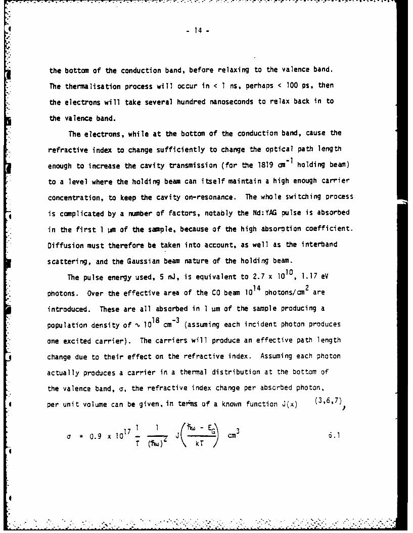
The pulse energy used, 5 nJ, is equivalent to 2.7 x 10¹⁰, 1.17 eV
14 2- Photons. Over the effective area of the CO beam 1014 ohotons/an are
introduced. These are all absorbed in 1urm of the sample producing a
population density of , 10 cm "3 (assuming each incident photon produces
one excited carrier). The carriers will produce an effective path length
change due to their effect on the refractive index. Assuming each photon
actually produces a carrier in a thermal distribution at the bottom of
the valence band, a, the refractive index change per abscrbed photon,
per unit volume can be given, in terft of a known function J(x) (3,6,7)
017 1 l 'G) E 3
a 0.9 X10 -J cm 6.1T(Iw)
I
I

-15
where T is the temperature in degrees Celsius and the photon energy 'W
is given in eVs. For the experimental conditions, the laser operating
at 1822 cm ,". 2 meV below the energy gap, and the temperature 77 K.
each carrier per unit volumne will change the refractive index seen by
the CO laser by a value a - 7x 10⁻¹ cm 3, thus giving a change ofrefractive index an a a W4M.5 in the first 1 pim of the sample, where all
the carriers are created.
To switch the cavity fromi completely off to completely on resonance
the path length change would be X/2 but, since the cavity is already held
close to the switch-up threshold by the CO laser field, only a change in
path length of X/20 is required. This means the change in refractive index
required would be an %, X/ZOL - 2.7 x 10⁻¹. The expression 6.1 is only
true for the Boltzmann regime where non-degenerate statistics can be used
to describe the carrier distributions in the semiconductor, so in this
case with carrier concentrations of 10 18 cm-3 it is clearly not accurate.
The value of a used is therefore the upper limit. Also in calculating
the carrier density, it has been assumed that each absorbed photon creates
only one carrier at the bottom of the band, whereas because of the high
4 energies to which the carriers are excited, Auger recombination may result
in the excitation of more than one excited carrier per absorbed photon.
It is in fact surprising that this theoretical calculation comes so
close to the experimental result. It should be noted that the short pulse
may be switching the cavity on at the optimum limit of the optical field
build up time of 8 ps.
The requirement for set-dng the switch up is that the Nd:YAG induced
carriers have to stay there long enough for the CO laser to maintain the
new increased carrier density itself, and so allow the resonator to maintain

-16-
itself on the upper branch of the hysteresis loop. The amount of time
required to do this can be shown to be of the order TR' the photoexcited
carrier recombination time. For an incident cw laser power of 26 mW at
. 1819 cm - on a 200 Wm spot diameter for a 210 um cavity length and a
measured absorption coefficient of 8 cm"1 2 x 10²¹ photons/cm3/sec are
absorbed. To hold the device on the upper branch it would take ", 150 ns
to generate enough extra excited carriers, which is comparable to the inter-
band recombination time. In the time taken for this to occur the carriers
induced by the Nd:YAG pulse will have diffused through a much larger volume
of the sample. The effect of diffusion out of the sample will be cancelled
* out by diffusion of carriers into the active volume, since the entire sample
has been irradiated by the Nd:YAG pulse. This will have the effect of
" causing the Nd:YAG induced carriers to spread throughout the sample length.
In the simple model where each carrier has the same effect on the refractive
index, the path length change is independent of the distribution of these
* induced carriers throughout the length of the sample [since An(Z) -!n(z)d )10
so to first order diffusion has no effect.
Bearing in mind the number of approximations made, the experimental
results agree very well with the theoretical predictions. This good
- agreement can be contrasted with that obtained by Starng et al .I)
They performed a similar experiment with a pulsed dye laser operating
-at 750 nm to make a GaAs bistable etalon, using a saturable excitonic
* absorotion. This etalon was then switched using a pulse f-om a dye laser
operating at 600 nm. The energy required to cause the etalon to switch
was over 100 times that calculated.
4 It should be possible to switch the cavity transmission up and down
- with the 35 ps pulse, by changing the optical length of the cavity by
. . ... " . *. . . .. . .-.-..- -., _ ,-2 -- .. , ... .: -. .. . . ," ' , ,

-17-
greater than X/2 and hence reaching the next interference order of the
etalon. As the carriers induced by the Nd:YAG pulse decayed away, the
cavity would relax back to the upper branch of the first bistable loop.
We attempted to detect this transient effect, but our detection system,
a Cu:Ge detector held at 4 K, with a Hewlett Packard 100 MHz-I.3 GHz
amplifier and a Tektronix 7104 oscilloscope, proved to be too insensitive.
Another method was used to get some information on the time dependence
of the switching.
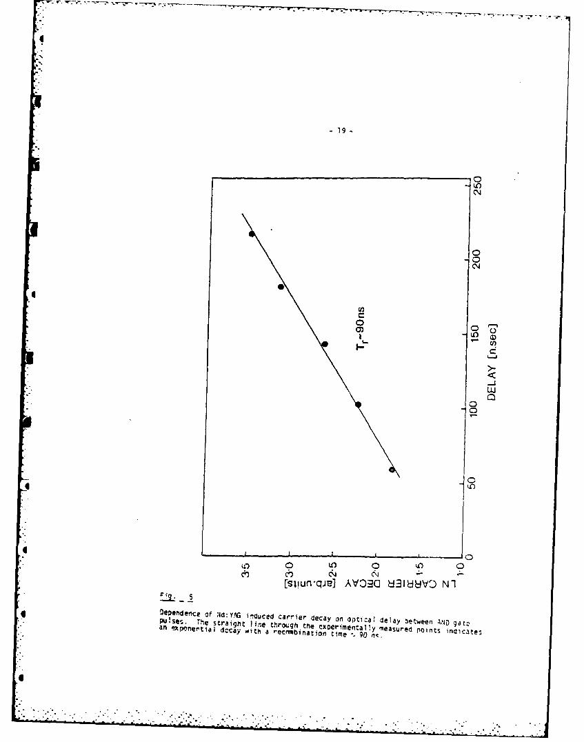
7 Measurement of Carrier Recombination Rate using Two External Pulses
The exact mechanism for introduction of carriers into the bottom of
the conduction band is not important. All that is required for the switching
is that enough refractive index change is induced by the "externally" excited
carriers for a long enough time for the cw laser to maintain a sufficiently
high population to hold the cavity in the higher transmission or on-resonance
state, or the device will fall back into the low transmission or off-resonance
state.
By temporally separating two pulses from the Nd:YAG laser a determination
of the excited carrier lifetime can be made. Whether two pulses with a fixed
delay have a cumulative effect in inducing switching depends on the recombination6
rate of the carriers excited by the first pulse and specifically how many of these
carriers remain when the second pulse arrives. The measurements were taken by
adjusting the first pulse on its own to switching threshold, then adjusting the
delayed pulse on its own to threshold. Both pulses were attenuated by a factor of
67

- 18 -
and allowed to be incident on the sample. The attenuation of the second
pulse was adjusted so that both pulses together caused switching. The pro-
cedure was then carried out for several fixed delays. By plotting the log
of the attenuation of the second pulse versus the delay between the two
pulses, a good fit was obtained to an exponential dependence of attenuation
on delay (figure 5). This fit implies that the carrier recombination occurs
exponentially with a recombination time of 90 ns. Since diffusion would
result in the distribution of carriers into the active volume, this should
be a bulk measurement. The value is significantly less than expected and
perhaps the initial carrier concentration at the front of the sample results
in Auger, radiative and surface effects, which would be complicated further
by diffusion.
The situation is complicated since Gaussian beam bistability, even in
a medium where n(I) a n0 + n21 exactly, has not been explained, and the
introduction of the microscopic mechanism for the non-linearity adds
another level of complexity, with diffusion and recombination entering
the problem.
This type of experiment can be extended to other cw holding powers
*to investigate the intensity dependence of the recombination time, and the
energy threshold of the system. Three orders of bistability can be
obtained allowing a wide range of intensities to oe covered.
0 Unfortunately this experiment is extremely hard to do. De~ays corresoonainq
to paths of over thirty metres are required which are very hard t.o set uo
L
0
. . ..
-19-
0
C\
@a
00C
I
L)L" O, > -,
0
L ©O
LO 10 (
F49 5 sI! un -qJe] AVOK:C a13lHl8VO NI
e~n~lnceof d:Y G nclcedcarierdecay on Optical delay between AND gat,-. D~~~ulses.. The straight I ine through the exeriena esud• ~~~~an exponertial decay with a recnmbination t~e 90 gOY. e citsi(1ce
,-"l{.'.
I-
• ." -.. • .- , ,- ..w

- 20-
PART 2
In attempting to extend.the low power band-gap resonant effects seen
in InSb at 77 K described in PART -1 to room temperatures, and to
different wavelengths, a tunable laser-like source of radiation is
required. In addition, an ultrashort pulse source would be desirable.
The dynamics of these effects are very interesting, not only from
a purely scientific point of view, but also for potential use in all
optical processing systems. The region we chose to investigate was
from 1.5 to 2.0 u, with materials such as GaSb, InGaAs and InGaAsP.
The growth techniques required to fabricate devices using these
materials are highly developed, and the potential use with semiconductor
. lasers and fibre optics was, and still is, a major motivation for fiture
work. The photon energies 600-830 meV are midway between those used in
the lnSb experiment (', 230 meV) and the photon energies used to observe
excitonic effects in GaAs (, 1.5 eV).
There are very few tunable laser sources in the 1.5-2.0 un spectra'
region, so very little semiconductor research with lasers has been done
in these materials. At the time this project was set up (1981) I.26 .1:i
pumped parametric oscillators and amplifiers were the only Proven syste,.
"low -center ( 2 ) lasers look pronising as tunable sources at these ,vave'enit,
* although they are still at the develocuent stage.

- 21 -
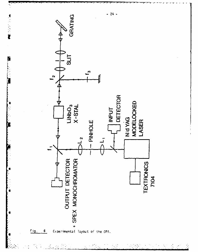
As a first stage in studying the nonlinearities in semiconductor
materials with energy gaps in the near infrared the construction of a novel
Nd:YAG pumped Lithium Niobate optical parametric amplifier has been funded
by the Science and Engineering Research Council, UK. A mode-locked Nd:YAG
laser, producing one single pulse approximately 35 ps long, with energies up
to 10mj, was used to optically pump a 5cm long lithium niobate crystal. The
system has been shown to be a useful sources of optical pulses of up to "04j
in the 1.5 to 2.12 mm region.
The unique design produces a relatively narrow bandwidth (less than 6cm - ),
with no long-term variation in wavelength, using a single crystal. This source
is ideal for our work in extending the low power non-linear effect, found in
InSb near 5 m at both 4K and 77K, to other semiconductor materials.
The pump laser, a .3 Lasers Nd:YAG system, produces single 35ps pulses
at 1. 0 6 m of energies up to 10uj and repetition rates of up to 10 Hz. Our
lithium niobate crystals are both 5 cm long cut with their optic axis at
450 to the front surface of the crystal. Both crystals are broad band A.R.
coated for 1.06pm and 1.6 to 2.04m. The crystal on which all the earlier
work was done was a 2cm diameter crystal on loan from Los Alamos National
Laboratories, and the later work was done on a 1cm diameter crystal purchased
from J.K. Lasers.
9 - 22-
'
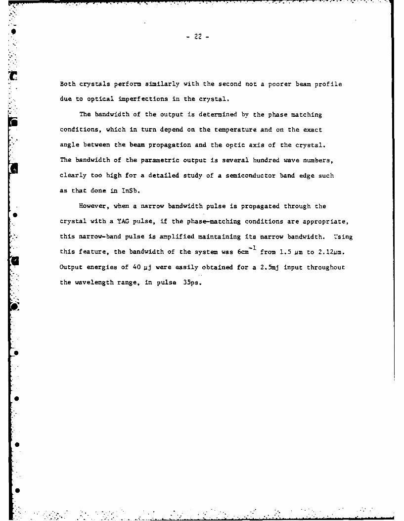
Both crystals perform similarly with the second not a poorer beam profile
due to optical imperfections in the crystal.
-The bandwidth of the output is determined by the phase matching
conditions, which in turn depend on the temperature and on the exact
angle between the beam propagation and the optic axis of the crystal.
The bandwidth of the parametric output is several hundred wave numbers,
clearly too high for a detailed study of a semiconductor band edge such
as that done in 1nSb.
However, when a narrow bandwidth pulse is propagated through theS
crystal with a YAG pulse, if the phase-matching conditions are appropriate,
" this narrow-band pulse is amplified maintaining its narrow bandwidth. Using
-1this feature, the bandwidth of the system was 6cm from 1.5 gm to 2.12gm.
Output energies of 40 Mj were easily obtained for a 2.Smj input throughout
the wavelength range, in pulse 35ps.
O
0
0
0- .- ,- i' ,:: : : . .,"

- 23-
CONCLUSIONS
a) This experiment has shown that an InSb bistable resonator held with a
5.3 pm laser beam can be switched using a 35ps, 5 nJ optical pulse at 1.06 m.
It acts as a test for our previously developed model of the refractive non-
linearity seen in InSb at 77K. The agreement between experiment and theory is
very good considering the number of uncertainties involved.
It is important here to emphasise the potential significance of this
result for device application of this non-linearity. The bistable resonator
has acted as an optical memory triggered by a 35ps pulse at a different
wavelength, and in the two pulse experiment as an optical AND gate. In this
case the inputs were provided by an ultrashort pulse from a Nd:YAG laser, but
the wavelength or coherence of the "external" pulse is immaterial as long as
it results in the creation of photoaxcited carriers. Indeed, switching has(18) Mcbeen demonstrated at Heriot-Watt using an electronic camera flashgun (18)
research is going on in this area of incoherent-to-coherent conversion.
b) We have a picosecond radiation source tunable from 1.5 to 2.1 Lm. Pulses
less than 35ps long can be produced at repetition rates of up to 1OHz.
Energies of between 5 and 204J are available across the tuning range. The beam
divergence is 25 mrad. The output is somewhat variable due to the erratic
pump laser output, but this has been overcome by using a minicomputer to
collect and process the data.
The utility of this system for the investigation of carrier dynamics in
semiconductors will be the subject of our continuing work, particularly in
the compounds Inl_Ga"Aa and In .. xGaxAsyPl.y.
-.6 " " -' . .2 .- . . . * . -. -'' - " . . .'' -: - " ' - - - - . : - - ''
. . . .; _ : .', . % • "" ", " • " - " " " - " - , "- " ' " ' ' ' " ' " -" - " " "' : ' " . .....
q CD -24-
6 z I C
CL
00
0-
ww.0L1
F ~ ~ Z o-w 60xeietllyu fteOA4W

-25-
References
(1) Optical Bistability (1981)edited by C.M. Bowden, M. Ciftan and H. Robl (Plenum, New York).
(2) E. Abraham and S.D. SmithRep. Prog. Phys. 45, 815 (1982).
(3) D.A.B. MillerLaser Focus, 79 (April 1982).
(4) H.M. Gibbs et al.Applied Physics Letters, 35, 245 (1979).
(5) C.T. Seaton, M.E. Prise and S.D. Smith* IQEC VI MOnchen
Abstracts published in Applied Physics B28(2,3), 132 (1982).
(6) S.D. Smith, C.T. Seaton, M.E. Prise, W.J. Firth, F. Tooley andC.R. Pidgeon16th ICPS Montpeliers, (1982).
(7) C.T. Seaton, S.D. Smith, F.A.P. Tooley, M.E. Prise and M.R. TaghizadehApplied Physics Letters 42(2), 131 (1983).
(8) F.S. Felber and J.H. MarburgerApplied Physics Letters 28, 731 (1976) and Phys. Rev. A17, 335 (1978).
(9) D.A.B. MillerIEEE J. Quantum Electronics 17, 306 (1981).
(10) W.J. Firth and E.M. WrightOptics Communications 40, 233 (1982).4
(11) E.M. WrightPhD Thesis, Heriot-Watt University, (1983).
(12) W.J. Firth, C.T. Seaton, S.D. Smith and E.M. WrightIQEC VI Manchen
* Abstract published in Applied Physics B28(2,3), 131 (1982).
(13) D.A.B. Miller and S.D. SmithApplied Optics 17, 380 (1979).
(14) D.A.B. MillerPhD Thesis, Heriot-Watt University, (1979).
(15) C.T. SeatonPhD Thesis, Heriot-Watt University, (1982).
(16) A. Miller, D.A.B. Miller and S.D. Smith* Advances in Physics, 30, 697-800 (1981).
: ." / -/ . . . ., , . . . .. . . . . . .. . .. . . . . .. V
-26-
(17) S. Starng, K. Tai, J.L. Jewell, N.M. Gibbs, A.C. Gossard, S.L. McCall,A. Passner, T.N.C. Venkatesan and W. WiegmannApplied Physics Letters 40, 205 (1982).
(18) F.A.P. Tooley, C.T. Seaton and S.D. Smithunpubl1i shed
MISSIONOf
Rawe Air Development CenterPRAVC ptanu and exec.ute6 tuemach, devetaPment, tu.t and6etecteed acqu.L4Ztion ptwgram icn .uppot~t 06 Commaond, ConttcZ* Cormuwica.tion4 and Intezene (C3 1) activites~. TechnicaZ* ~and eng-&eMng AuPPO~t 4U~hin axea.6 o6 technica2 competence~4 ptowided to ESV PjtogvaM 066ice (POA) and otAVL ESVeme.,t46. The ptnciPaZ -technZcaZ rr64ion mreaa m~e
comunlc.ation6, etectomagnetic guidance and controZ, 6uAvuiUanCe 06 940 und and av~o~ pace object6, -i-nteZ9ence datacoZection and kandting, indo~maioon 6y.6-tem .technaooy,,6otd 6tate 6c.enca.~, eteettomo.gnetic and ete-toniZcteiabZtitY, maintabitity and compcatbZLzity.

FILMED
2-85
* DTIC