unit 3 quadrature carrier multiplexing - atria | e …...analog communication (10ec53) prashanth cr,...
TRANSCRIPT
Analog Communication (10EC53)
Prashanth CR, Asst. Professor, ECE, Vemana Institute of Technology, B’lore 1
Unit 3
Quadrature Carrier Multiplexing
A Quadrature Carrier Multiplexing (QCM) or Quadrature Amplitude Modulation (QAM)
method enables two DSBSC modulated waves, resulting from two different message
signals to occupy the same transmission band width and two message signals can be
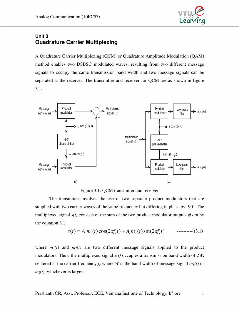
separated at the receiver. The transmitter and receiver for QCM are as shown in figure
3.1.
Figure 3.1: QCM transmitter and receiver
The transmitter involves the use of two separate product modulators that are
supplied with two carrier waves of the same frequency but differing in phase by -90o. The
multiplexed signal s(t) consists of the sum of the two product modulator outputs given by
the equation 3.1.
---------- (3.1)
where m1(t) and m2(t) are two different message signals applied to the product
modulators. Thus, the multiplexed signal s(t) occupies a transmission band width of 2W,
centered at the carrier frequency fc where W is the band width of message signal m1(t) or
m2(t), whichever is larger.
)2sin()()2cos()()( 21 tftmAtftmAts cccc ππ +=
Analog Communication (10EC53)
Prashanth CR, Asst. Professor, ECE, Vemana Institute of Technology, B’lore 2
At the receiver, the multiplexed signal s(t) is applied simultaneously to two separate
coherent detectors that are supplied with two local carriers of the same frequency but
differing in phase by -90o. The output of the top detector is ( )tmAc 12
1 and that of the
bottom detector is ( )tmAc 221 .
For the QCM system to operate satisfactorily, it is important to maintain correct
phase and frequency relationships between the local oscillators used in the transmitter
and receiver parts of the system.
Hilbert transform
The Fourier transform is useful for evaluating the frequency content of an energy
signal, or in a limiting case that of a power signal. It provides mathematical basis for
analyzing and designing the frequency selective filters for the separation of signals on the
basis of their frequency content. Another method of separating the signals is based on
phase selectivity, which uses phase shifts between the appropriate signals (components)
to achieve the desired separation.
In case of a sinusoidal signal, the simplest phase shift of 180o is obtained by
“Ideal transformer” (polarity reversal). When the phase angles of all the components of a
given signal are shifted by 90o, the resulting function of time is called the “Hilbert
transform” of the signal.
Consider an LTI system with transfer function defined by equation 3.2.
----------------- (3.2)
and the Signum function given by
The function H(f) can be expressed using Signum function as given by 3.3.
--------------------- (3.3)
( )
<
=
>−
=
0,
0,0
0,
fj
f
fj
fH
( )
<−
=
>
=
0,1
0,0
0,1
sgn
f
f
f
f
( ) ( )fjfH sgn−=

Analog Communication (10EC53)
Prashanth CR, Asst. Professor, ECE, Vemana Institute of Technology, B’lore 3
We know that , and .
Therefore,
Thus the magnitude for all f, and angle
The device which possesses such a property is called Hilbert transformer. When
ever a signal is applied to the Hilbert transformer, the amplitudes of all frequency
components of the input signal remain unaffected. It produces a phase shift of -90o for all
positive frequencies, while a phase shift of 90o
for all negative frequencies of the signal.
If x(t) is an input signal, then its Hilbert transformer is denoted by ( )tx̂ and
shown in the following diagram.
To find impulse response h(t) of Hilbert transformer with transfer function H(f).
Consider the relation between Signum function and the unit step function.
Differentiating both sides with respect to t,
Apply Fourier transform on both sides,
Applying duality property of Fourier transform,
Hilbert Transformer ( )tx ( )tx̂
( )
<
>=
−
0,1
0,1
2
2
fe
fefH
j
j
π
π
( ) ,1=fH
( )
<+
>−=∠
0,2
0,2
f
ffH
π
π
( ) ( ) ( ),12sgn txtut =−=
( ){ } ( )ttxdt
dδ2=
( )ωj
t2
sgn ↔ ( )fj
tπ
1sgn ↔
( )tj
fSgnπ
1↔−
jej
−=−
21π
jej
=21π ( ) ( )θθθ sincos je
j ±=±

Analog Communication (10EC53)
Prashanth CR, Asst. Professor, ECE, Vemana Institute of Technology, B’lore 4
We have
Therefore the impulse response h(t) of an Hilbert transformer is given by the
equation 3.4,
-------------------- (3.4)
Now consider any input x(t) to the Hilbert transformer, which is an LTI system.
Let the impulse response of the Hilbert transformer is obtained by convolving the input
x(t) and impulse response h(t) of the system.
-------------------- (3.5)
The equation 3.5 gives the Hilbert transform of x(t).
The inverse Hilbert transform x(t) is given by
-------------------- (3.6)
We have
The Fourier transform ( )fX̂ of ( )tx̂ is given by
-------------------- (3.7)
( )t
thπ
1=
( ) ( ) ( )thtxtx ∗=ˆ
( ) ( )t
txtxπ
1ˆ ∗=
( ) ( )( )∫
+∞
∞−−
= ττ
τ
πd
t
xtx
1ˆ
( ) ( )( )∫
+∞
∞−−
−= τ
τ
τ
πd
t
xtx
ˆ1
( ) ( ) ( )thtxtx ∗=ˆ
( ) ( ) ( )fHfXfX =ˆ
( ) ( ) ( )fXfjfX sgnˆ −=
( )t
fHπ
1↔
( ) ( )fjfH sgn−=
Analog Communication (10EC53)
Prashanth CR, Asst. Professor, ECE, Vemana Institute of Technology, B’lore 5
Applications of Hilbert transform
1. It is used to realize phase selectivity in the generation of special kind of
modulation called Single Side Band modulation.
2. It provides mathematical basis for the representation of band pass signals.
Note: Hilbert transform applies to any signal that is Fourier transformable.
Example: Find the Hilbert transform of .
This represents Fourier transform of the sine function. Therefore the Hilbert
transform of cosine function is sin function given by
Pre-envelope
Consider a real valued signal x(t). The pre-envelope ( )tx+ for positive frequencies
of the signal x(t) is defined as the complex valued function given by equation 3.8.
( ) ( ) ( )txjtxtx ˆ+=+ ------------------ (3.8)
Apply Fourier transform on both the sides,
( ) ( ) ( ) ( )[ ]fXfjjfXfX sgn−+=+
( ) )2cos( tftx cπ=
( ) ( ) ( )[ ]cc fffffX ++−= δδ2
1
( ) ( ) ( )fXfjfX sgnˆ −=
( ) ( ) ( ) ( )[ ]cc fffffjfX ++−−= δδ2
1sgnˆ
( ) ( ) ( )[ ]cc ffffj
fX +−−= δδ2
1ˆ
( ) ( ) ( )[ ]cc ffffj
fX +−−= δδ2
1ˆ
( ) )2sin(ˆ tftx cπ=

Analog Communication (10EC53)
Prashanth CR, Asst. Professor, ECE, Vemana Institute of Technology, B’lore 6
( )( )
( )
<
=
>
=+
0,0
0,0
0,2
f
fX
ffX
fX -------------------- (3.9)
The pre-envelope ( )tx− for negative frequencies of the signal is given by
( ) ( ) ( )txjtxtx ˆ−=−
The two pre-envelopes ( )tx+ and ( )tx− are complex conjugate of each other,
that is ( ) ( )*txtx −+ =
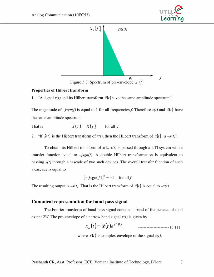
The spectrum of the pre-envelope ( )tx+ is nonzero only for positive frequencies
as emphasized in equation 3.9. Hence plus sign is used as a subscript. In contrast, the
spectrum of the other pre-envelope ( )tx− is nonzero only for negative frequencies. That
is
( ) ( )( )
<
=
>
=−
0,2
0,0
0,0
ffX
fX
f
fX ------------------- (3.10)
Thus the pre-envelopes ( )tx+ and ( )tx− constitute a complementary pair of
complex valued signals.
Figure 3.2: Spectrum of the low pass signal x(t)
X(0)
W f
( )fX
Analog Communication (10EC53)
Prashanth CR, Asst. Professor, ECE, Vemana Institute of Technology, B’lore 7
Figure 3.3: Spectrum of pre-envelope ( )tx+
Properties of Hilbert transform
1. “A signal x(t) and its Hilbert transform ( )tx̂ have the same amplitude spectrum”.
The magnitude of –jsgn(f) is equal to 1 for all frequencies f. Therefore x(t) and ( )tx̂ have
the same amplitude spectrum.
That is ( ) ( )fXfX =ˆ for all f
2. “If ( )tx̂ is the Hilbert transform of x(t), then the Hilbert transform of ( )tx̂ , is –x(t)”.
To obtain its Hilbert transform of x(t), x(t) is passed through a LTI system with a
transfer function equal to –jsgn(f). A double Hilbert transformation is equivalent to
passing x(t) through a cascade of two such devices. The overall transfer function of such
a cascade is equal to
[ ] 1)sgn(2
−=− fj for all f
The resulting output is –x(t). That is the Hilbert transform of ( )tx̂ is equal to –x(t).
Canonical representation for band pass signal
The Fourier transform of band-pass signal contains a band of frequencies of total
extent 2W. The pre-envelope of a narrow band signal x(t) is given by
( ) ( ) tfj cetxtxπ2~=+ , ---------------------- (3.11)
where ( )tx~ is complex envelope of the signal x(t).
2X(0) ( )fX +
f W

Analog Communication (10EC53)
Prashanth CR, Asst. Professor, ECE, Vemana Institute of Technology, B’lore 8
Figure 3.4: Spectrum of the band pass signal x(t)
Figure 3.5: Spectrum of the pre-envelope ( )tx+
Figure 3.6: spectrum of the complex envelope ( )tx~
Figure 3.4 shows the amplitude spectrum of band pass signal x(t). Figure 3.5
shows amplitude spectrum of pre envelope ( )tx+ . Figure 3.6 shows amplitude spectrum of
complex envelope ( )tx~ .
Equation 3.11 is the basis of definition for complex envelope ( )tx~ in terms of pre-
envelope ( )tx+ . The spectrum of ( )tx+ is limited to the frequency band
( )cfX
( )fX
( )cfX2
( )cfX2
fc -fc f fc-+w
f fc fc-+w fc--w
( )fX +
f 0 w
( )fX~

Analog Communication (10EC53)
Prashanth CR, Asst. Professor, ECE, Vemana Institute of Technology, B’lore 9
wffwf cc +<<− as shown in figure 3.5. Therefore, applying the frequency-shift
property of Fourier transform to equation 3.11, we find that the spectrum of the complex
envelope ( )tx~ is limited to the band wfw <<− and centered at the origin as shown in
figure 3.6. That is, the complex envelope ( )tx~ of a band pass signal x(t) is a low-pass
signal.
Given signal x(t) is the real part of the pre-envelope ( )tx+ . So, we express the
original band pass signal x(t) in terms of the complex envelope ( )tx~ , as follows
------------------- (3.12)
But ( )tx~ is a complex quantity.
------------------- (3.13)
where and are both real valued low pass functions. This low pass property is
inherited from the complex envelope ( )tx~ . Therefore original band pass signal x(t) is
expressed in canonical form by using equations 3.12 and 3.13 as follows.
------------- (3.14)
where is “in-phase component” and is “quadrature component” of the band
pass signal x(t). This nomenclature recognizes that ( )tf cπ2sin is in phase-quadrature
with respect to ( )tf cπ2cos .
Both and are low-pass signals limited to the band wfw <<− .
Hence, except for scaling factors, they may be derived from the band pass signal x(t)
using the block diagram shown 3.7.
( ) ( )[ ]tfj cetxtxπ2~Re=
( ) ( ) ( )tjxtxtx QI +=~
( )txI( )txQ
( ) ( )[ ]tfj cetxtxπ2~Re=
( ) ( ) ( )[ ]fctj
Q
tfj
I etjxetxtx c ππ 22Re +=
( ) ( ) ( ) ( )[ ] ( ) ( ) ( )[ ][ ]tfjtftjxtfjtftxtx ccQccI ππππ 2sin2cos2sin2cosRe +++=
( ) ( ) ( ) ( )tfxtftxtx cQcI ππ 2sin2cos −=
( )txI( )txQ
( )txI ( )txQ

Analog Communication (10EC53)
Prashanth CR, Asst. Professor, ECE, Vemana Institute of Technology, B’lore 10
Figure 3.7: Block diagram to produce in-phase and quadrature components
Single Side Band Suppressed Carrier modulation
Standard AM and DSBSC require transmission bandwidth equal to twice the
message bandwidth. In both the cases spectrum contains two side bands of width W Hz,
each. But the upper and lower sides are uniquely related to each other by the virtue of
their symmetry about the carrier frequency. That is, given the amplitude and phase
spectra of either side band, the other can be uniquely determined. Thus if only one side
band is transmitted, and if both the carrier and the other side band are suppressed at the
transmitter, no information is lost. This kind of modulation is called SSBSC and spectral
comparison between DSBSC and SSBSC is shown in the figures 3.8 and 3.9.
Figure 3.8: Spectrum of the DSBSC wave
Figure 3.9: Spectrum of the SSBSC wave
( )tx
( )txQ2
1−
Low Pass
Filter
Low Pass
Filter
Oscillator )2cos( tfcπ
)2sin( tfcπ
*
-90o
Phase
Shifter
( )txI2
1
*

Analog Communication (10EC53)
Prashanth CR, Asst. Professor, ECE, Vemana Institute of Technology, B’lore 11
Frequency-domain description: -
Consider a message signal m(t) with a spectrum M(f) band limited to the interval
wfw <<− as shown in figure 3.10, the DSBSC wave obtained by multiplexing m(t) by
the carrier wave and is also shown, in figure 3.11. The upper side band
is represented in duplicate by the frequencies above fc and those below -fc, and when only
upper
Figure 3.10: Spectrum of message wave
Figure 3.11: Spectrum of DSBSC wave
Figure 3.12: Spectrum of SSBSC-LSB wave
Figure 3.13: Spectrum of SSBSC-USB wave
M(f)
SDSB(f)
SSSB(f)
SSSB(f)
( ) )2cos( tfAtc cc π=
w 0 -w
fc+w -fc-w -fc+w fc-w -fc fc 0
fc-w -fc+w -fc fc
fc+w -fc-w -fc fc

Analog Communication (10EC53)
Prashanth CR, Asst. Professor, ECE, Vemana Institute of Technology, B’lore 12
side band is transmitted; the resulting SSB modulated wave has the spectrum shown in
figure 3.13. Similarly, the lower side band is represented in duplicate by the frequencies
below fc and those above -fc and when only the lower side band is transmitted, the
spectrum of the corresponding SSB modulated wave shown in figure 3.12. Thus the
essential function of the SSB modulation is to translate the spectrum of the modulating
wave, either with or without inversion, to a new location in the frequency domain.
The advantage of SSB modulation is reduced bandwidth and the elimination of
high power carrier wave. The main disadvantage is the cost and complexity of its
implementation.
Frequency Discrimination Method for generating an SSBSC modulated wave
Consider the generation of SSB modulated signal containing the upper side band
only. From a practical point of view, the most severe requirement of SSB generation
arises from the unwanted sideband, the nearest component of which is separated from the
desired side band by twice the lowest frequency component of the message signal. It
implies that, for the generation of an SSB wave to be possible, the message spectrum
must have an energy gap centered at the origin as shown in figure 3.14. This requirement
is naturally satisfied by voice signals, whose energy gap is about 600Hz wide.
Figure 3.14: Message spectrum with energy gap at the origin
The frequency discrimination or filter method of SSB generation consists of a
product modulator, which produces DSBSC signal and a band-pass filter to extract the
desired side band and reject the other and is shown in the figure 3.15.
M(f)
f 0

Analog Communication (10EC53)
Prashanth CR, Asst. Professor, ECE, Vemana Institute of Technology, B’lore 13
Figure 3.15: Frequency discriminator to generate SSBSC wave
Application of this method requires that the message signal satisfies two conditions:
1. The message signal m(t) has no low-frequency content.
Example: - speech, audio, music.
2. The highest frequency component W of the message signal m(t) is much less than the
carrier frequency fc.
Then, under these conditions, the desired side band will appear in a non-overlapping
interval in the spectrum in such a way that it may be selected by an appropriate filter. In
designing the band pass filter, the following requirements should be satisfied:
1) The pass band of the filter occupies the same frequency range as the spectrum of the
desired SSB modulated wave.
2. The width of the guard band of the filter, separating the pass band from the stop band,
where the unwanted sideband of the filter input lies, is twice the lowest frequency
component of the message signal.
When it is necessary to generate an SSB modulated wave occupying a frequency
band that is much higher than that of the message signal, it becomes very difficult to
design an appropriate filter that will pass the desired side band and reject the other. In
such a situation it is necessary to resort to a multiple-modulation process so as to ease the
filtering requirement. This approach is illustrated in the following figure 3.16 involving
two stages of modulation.

Analog Communication (10EC53)
Prashanth CR, Asst. Professor, ECE, Vemana Institute of Technology, B’lore 14
Figure 3.16: Two stage frequency discriminator
The SSB modulated wave at the first filter output is used as the modulating wave
for the second product modulator, which produces a DSBSC modulated wave with a
spectrum that is symmetrically spaced about the second carrier frequency f2. The
frequency separation between the side bands of this DSBSC modulated wave is
effectively twice the first carrier frequency f1, there by permitting the second filter to
remove the unwanted side band.
Time-domain description
The time domain description of an SSB wave s(t) in the canonical form is given
by the equation 3.15.
-------------------- (3.15)
where SI(t) is the in-phase component of the SSB wave and SQ(t) is its quadrature
component. The in-phase component SI(t) except for a scaling factor, may be derived
from S(t) by first multiplying S(t) by ( )tf cπ2cos and then passing the product through a
low-pass filter. Similarly, the quadrature component SQ(t), except for a scaling factor,
may be derived from s(t) by first multiplying s(t) by ( )tfcπ2sin and then passing the
product through an identical filter.
The Fourier transformation of SI(t) and SQ(t) are related to that of SSB wave as
follows, respectively.
------------------- (3.16)
------------------- (3.17)
where wfw <<− defines the frequency band occupied by the message signal m(t).
Product
Modulator1
Product
Modulator2
Band
Pass Filter
Band
Pass Filter
( )tm
( )tfAc 22cos π( )tfAc 12cos π
( )ts( )ts1
SSB
wave
( ) ( ) ( ) ( )tftstftsts cQcI ππ 2sin)(2cos −=
( )( ) ( )
≤≤−++−
=elsewhere
wfwffSffSfS
cc
I,0
,
( )( ) ( )[ ]
≤≤−+−−
=elsewhere
wfwffSffSjfS
cc
Q,0
,
Analog Communication (10EC53)
Prashanth CR, Asst. Professor, ECE, Vemana Institute of Technology, B’lore 15
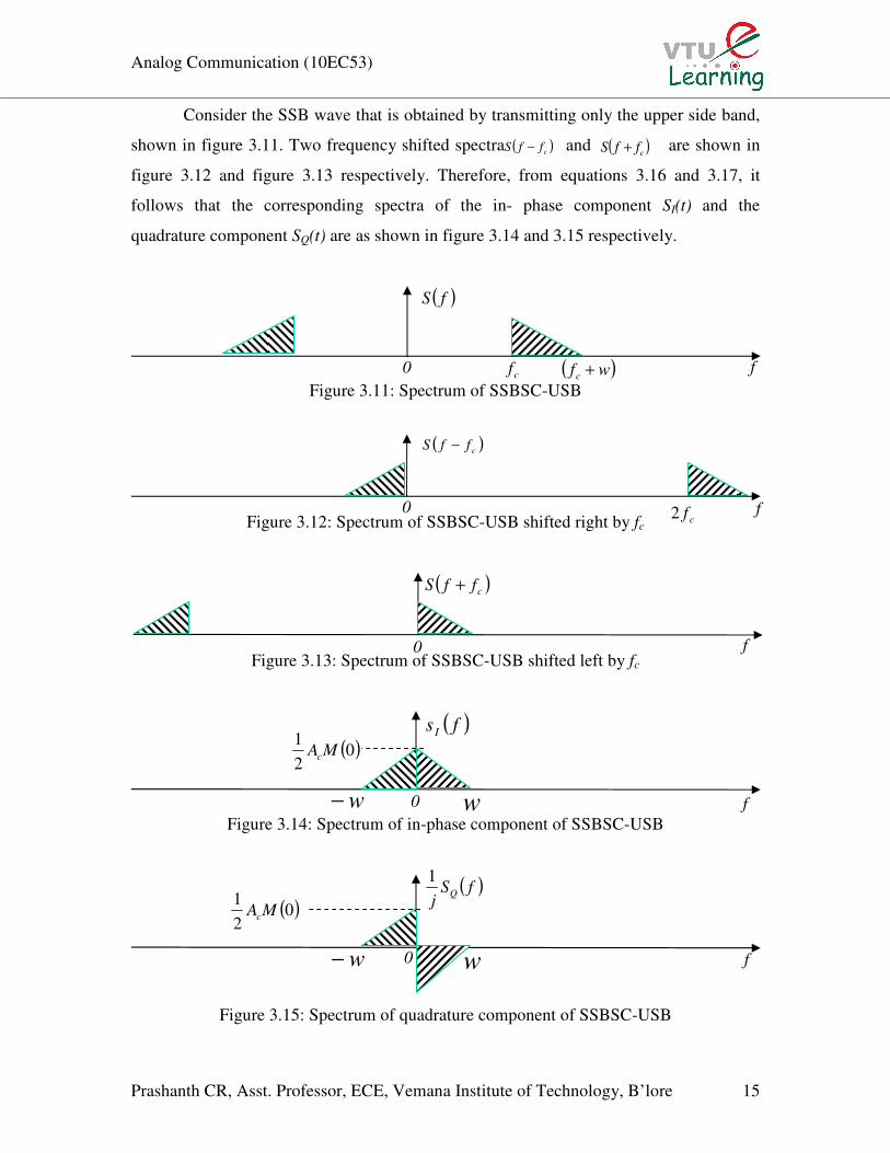
Consider the SSB wave that is obtained by transmitting only the upper side band,
shown in figure 3.11. Two frequency shifted spectra and are shown in
figure 3.12 and figure 3.13 respectively. Therefore, from equations 3.16 and 3.17, it
follows that the corresponding spectra of the in- phase component SI(t) and the
quadrature component SQ(t) are as shown in figure 3.14 and 3.15 respectively.
Figure 3.11: Spectrum of SSBSC-USB
Figure 3.12: Spectrum of SSBSC-USB shifted right by fc
Figure 3.13: Spectrum of SSBSC-USB shifted left by fc
Figure 3.14: Spectrum of in-phase component of SSBSC-USB
Figure 3.15: Spectrum of quadrature component of SSBSC-USB
( )fS
( )cffS −
( )cffS +
( )02
1MAc
( )fs I
ww−
( )02
1MAc
0
( )cffS − ( )cffS +
cf ( )wfc +
cf2
w− w
( )fSj
Q
1
f 0
0
0
0
f
f
f
f

Analog Communication (10EC53)
Prashanth CR, Asst. Professor, ECE, Vemana Institute of Technology, B’lore 16
From the figure 3.14, it is found that
where M(f) is the Fourier transform of the message signal m(t). Accordingly in-phase
component SI(t) is defined by equation 3.18.
------------------- (3.18)
Now on the basis of figure 3.15, it is found that
------------------- (3.19)
where is the Signum function.
But from the discussions on Hilbert transforms, it is shown that
------------------- (3.20)
where ( )fM̂ is the Fourier transform of the Hilbert transform of m(t). Hence the
substituting equation (3.20) in (3.19), we get
------------------------- (3.21)
Therefore quadrature component ( )tsQ is defined by equation 3.22.
-------------------------- (3.22)
Therefore substituting equations (3.18) and (3.22) in equation in (3.15), we find
that canonical representation of an SSB wave s(t) obtained by transmitting only the upper
side band is given by the equation 3.23.
-------------- (3.23)
Following the same procedure, we can find the canonical representation for an SSB wave
s(t) obtained by transmitting only the lower side band is given by
( ) ( )fMAfS cI2
1=
( ) ( )tmAts cI2
1=
( )
( )
( )
<
=
>−
=
0,2
0,0
0,2
ffMAj
f
ffMAj
fS
c
c
Q
( ) ( )fMfAj
fS cQ sgn2
)(−
=
( )fsgn
( ) ( ) ( )fMfMfj ˆsgn =−
( ) ( )fMAfS cQˆ
2
1=
( ) ( )tmAts cQˆ
2
1=
( ) ( ) ( ) ( ) ( )tftmAtftmAts ccccU ππ 2sinˆ2
12cos
2
1−=

Analog Communication (10EC53)
Prashanth CR, Asst. Professor, ECE, Vemana Institute of Technology, B’lore 17
-------------- (3.24)
Phase discrimination method of SSB generation
Time domain description of SSB modulation leads to another method of SSB
generation using the equations (3.23) or (3.24). The block diagram of phase discriminator
is as shown in figure 3.16.
Figure 3.16: Block diagram of phase discriminator
The phase discriminator consists of two product modulators I and Q, supplied
with carrier waves in-phase quadrature to each other. The incoming base band signal m(t)
is applied to product modulator I, producing a DSBSC modulated wave that contains
reference phase sidebands symmetrically spaced about carrier frequency fc. The Hilbert
transform ( )tm̂ of m(t) is applied to product modulator Q, producing a DSBSC
modulated that contains side bands having identical amplitude spectra to those of
modulator I, but with phase spectra such that vector addition or subtraction of the two
modulator outputs results in cancellation of one set of side bands and reinforcement of
the other set. The use of a plus sign at the summing junction yields an SSB wave with
only the lower side band, whereas the use of a minus sign yields an SSB wave with only
the upper side band. This modulator circuit is called Hartley modulator.
Single –tone SSB-LSB modulation
Consider a single-tone message signal and its Hilbert
transform . Substituting these in equation (3.24), we get
-90o Phase
Shifter
Product
Modulator Q
-90o Phase
Shifter
Product
Modulator I
Oscillator
∑
( )tfA cc π2cos
( )tfA cc π2sin
±
+( )tm
( )tm̂
( )tsIn-phase path
Quadrature path
( ) ( ) ( ) ( ) ( )tftmAtftmAts ccccL ππ 2sinˆ2
12cos
2
1+=
( ) ( )tfAtm mm π2cos=
( ) ( )tfAtm mm π2sinˆ =
Analog Communication (10EC53)
Prashanth CR, Asst. Professor, ECE, Vemana Institute of Technology, B’lore 18
------------------ (3.25)
Therefore the single tone SSBSC wave is a sinusoidal wave of frequency equal to
sum/ difference of carrier and message frequencies for USB/LSB.
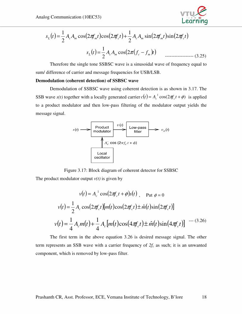
Demodulation (coherent detection) of SSBSC wave
Demodulation of SSBSC wave using coherent detection is as shown in 3.17. The
SSB wave s(t) together with a locally generated carrier is applied
to a product modulator and then low-pass filtering of the modulator output yields the
message signal.
Figure 3.17: Block diagram of coherent detector for SSBSC
The product modulator output v(t) is given by
, Put 0=φ
--- (3.26)
The first term in the above equation 3.26 is desired message signal. The other
term represents an SSB wave with a carrier frequency of 2fc as such; it is an unwanted
component, which is removed by low-pass filter.
( ) ( ) ( ) ( ) ( )tftfAAtftfAAts cmmccmmcL ππππ 2sin2sin2
12cos2cos
2
1+=
( ) ( )( )tffAAts mcmcL −= π2cos2
1
( ) )2cos(1
φπ += tfAtc cc
( ) ( ) ( )tstfAtv cc φπ += 2cos1
( ) ( ) ( ) ( ) ( ) ( )[ ]tftmtftmtfAtv cccc πππ 2sinˆ2cos2cos2
1±=
( ) ( ) ( ) ( ) ( ) ( )[ ]tftmtftmAtmAtv cccc ππ 4sinˆ4cos4
1
4
1±+=