comparison between quadrature- and polar-modulation ... · comparison between quadrature- and...
TRANSCRIPT
Comparison between Quadrature- and Polar-modulation Switching-mode Transmitter with Pulse-density Modulation
Abstract— This paper presents the performance of the quadrature modulation (QM) transmitter when compared with the (PM) transmitter. So as to evaluate the substantive power efficiency in both transmitters, the effective demodulation power efficiency (EDPE) is proposed as a novel figure of merit for transmitters. Computer simulation reveals that the EDPE for a QM transmitter is lower than that for a PM transmitter. In addition, D/U for a QM transmitter is higher than the one for PM transmitter due to lower quantization noise. As a result, the EVMs for a QM transmitter is higher than the one for a PM transmitter.
Keywords— Transmitter; Polar modulation; Quadrature modulation; Pulse density modulation; Delta-sigma modulation; Effective demodulation power efficiency
I. INTRODUCTION Around a half of the power consumption in a mobile
communication transmitter is consumed in a power amplifier. Therefore, reducing power consumption in a power amplifier is indispensable so as to save energy in mobile communications. To reduce power consumption in a transmitter, highly-power-efficient transmitters using envelope pulse-width- or pulse-density-modulation [1]-[10] have been investigated intensively so far. This type of transmitters can amplify signals linearly with keeping high power efficiency even when a backoff from the saturation power of a power amplifier is large, whereas conventional transmitters using class-A, AB, or B amplifiers cannot. In addition, the transmitters using delta-sigma modulation for pulse-density modulation [1]-[3], [5]-[10] is attractive because it can reduce quantum noise by noise shaping. Among these types of transmitters polar-modulation (PM) [2]-[5] and quadrature-modulation (QM) transmitters [6]-[10] mitigate the requirements in high-speed operation of delta-sigma (Δ−Σ) modulators compared with the transmitters using bandpass Δ−Σ modulation in pulse-density modulation [1].
The PM transmitters separate a modulated baseband signal to envelope and phase components, amplify the envelope component, and restore them at or in front of the power amplifier. However, the PM transmitter needs analog signal processing in a phase modulator that generates constant-envelope RF phase-modulated signal. In contrast, the QM transmitter is advantageous in compatibility to LSIs because all-signal processing can be
done by digital circuits. However, comparison between the PM and QM transmitters has not been performed sufficiently. In addition, the effective power efficiency from the output of the transmitter and the demodulated signal at the receiver has not yet been evaluated for the QM transmitter.
This paper presents the performance of the QM transmitter when compared with the PM transmitter. So as to evaluate the substantive power efficiency in both transmitters, the effective demodulation power efficiency (EDPE) is proposed as a novel figure of merit for transmitters. Computer simulation reveals that the maximum EDPE in a QM transmitter is lower than the one in a PM transmitter.
II. TRANSMITTER ARCHITECTURE
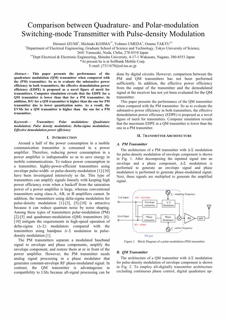
A. PM Transmitter The architecture of a PM transmitter with Δ-Σ modulation
for pulse-density modulation of envelope component is shown in Fig. 1. After decomposing the inputted signal into an envelope and a phase component, Δ-Σ modulation is performed to generate an envelope signal and phase modulation is performed to generate phase-modulated signal. Next, these signals are multiplied to generate the amplified signal.
Figure 1. Block Diagram of a polar-modulation (PM) transmitter
B. QM Transmitter The architecture of a QM transmitter with Δ-Σ modulation
for pulse-density modulation of envelope component is shown in Fig. 2. To employ all-digitally transmitter architecture excluding continuous phase control, digital quadrature up-
Hironori IZUMI†, Michiaki KOJIMA†*, Yohtaro UMEDA†, Osamu TAKYU†† †Department of Electrical Engineering, Graduate School of Science and Technology, Tokyo University of Science,
2641 Yamazaki, Noda, Chiba, 278-8510 Japan ††Dept Electrical & Electronic Engineering, Shinshu University, 4-17-1 Wakasato, Nagano, 380-8553 Japan
*At present he is at Softbank Mobile Corp. E-mail: [email protected]
PAPA
φ(t) : phase:carrier frequency
PM part
Phase extraction
Envelope extraction
I-ch Input
PhaseModulator
Δ−ΣModulator
: sampling frequencyfs
fc
A(t) : envelope
BPFQ-ch Input
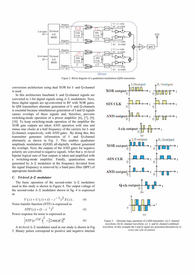
conversion architecture using dual XOR for I- and Q-channel is used.
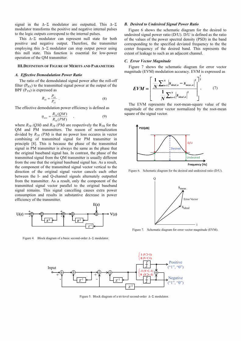
In this architecture baseband I- and Q-channel signals are converted to 1-bit digital signals using Δ−Σ modulators. Next, these digital signals are up-converted to RF with XOR gates. In QM transmitters alternate generation of I- and Q-channels is essential because simultaneous generation of I and Q signals causes overlaps of these signals and, therefore, prevents switching-mode operation of a power amplifier [6], [7], [9], [10]. To keep switching-mode operation of the amplifier the XOR gate outputs are taken AND operation with sine and minus sine clocks at a half frequency of the carriers for I- and Q-channel, respectively, with AND gates. By doing this, this transmitter generates information of I- and Q-channel alternately as shown in Fig. 3. This enables quadrature amplitude modulation (QAM) all-digitally without generated the overlaps. Next, the outputs of the AND gates for negative polarity are converted to negative signals. After that a tri-level bipolar logical sum of four outputs is taken and amplified with a switching-mode amplifier. Finally, quantization noise generated by Δ−Σ modulator at the frequency deviated from the signal frequency is removed by a band pass filter (BPF) of appropriate bandwidth.
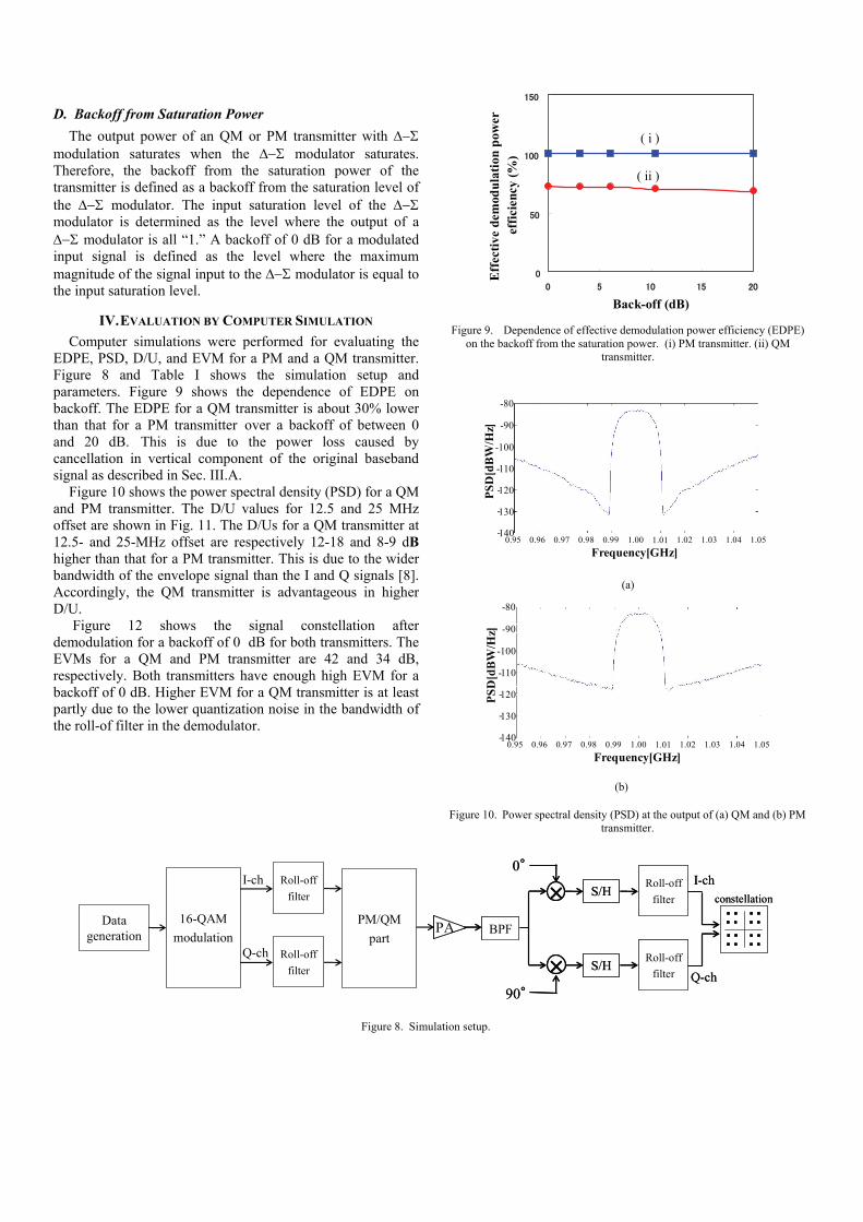
C. Tri-level Δ−Σ modulator The basic operation of the second-order Δ−Σ modulator
used in this study is shown in Figure 4. The output voltage of the second-order Δ−Σ modulator shown in fig. 4 is expressed as
)(2)11()()( zEzzUzV −−+= , (4) Noise transfer function (NTF) is expressed as
21)1()( −−= zzNTF (5) Power response for noise is expressed as
[ ]422 )sin(2)( feNTF fj ππ = (6)
A tri-level Δ−Σ modulator used in our study is shown in Fig. 5. Binary pulses correspond to positive and negative internal
(a)
(b)
.(c)
Figure 3. Alternate logic operation of a QM transmitter. (a) I- channel waveform. (b) Q- channel waveform. (c) I- and Q- channel combined
waveform. In this example the I and Q signal are generated alternatively in every one cyle of carriers.
BPFPA
I-ch input
Q-ch input
COSCLK
SINCLK
-SINCLK
-SINCLK
fcfc/2
fc/2fc
XORXORPositive
(“1”,”0”)
Negative(“1”,”0”)
XORXOR
XORXOR
XORXOR
Tri-levelΔ-Σ
MODANDAND
ANDAND
ANDAND
ANDAND
“1”:+1→ON“0”: 0→OFF
“1”:-1→ON“0”: 0→OFF
“1”:+1→ON“0”: 0→OFF
“1”:-1→ON“0”: 0→OFF
QM part
Tri-levelΔ-Σ
MOD
Positive(“1”,”0”)
Negative(“1”,”0”)
Figure 2. Block diagram of a quadrature-modulation (QM) transmitter.
signal in the Δ−Σ modulator are outputted. This Δ−Σ modulator transforms the positive and negative internal pulses to the logic outputs correspond to the internal pulses.
This Δ−Σ modulator can represent null state for both positive and negative output. Therefore, the transmitter employing this Δ−Σ modulator can stop output power using this null state. This function is essential for low-power operation of the QM transmitter.
III. DEFINITION OF FIGURE OF MERITS AND PARAMETERS
A. Effective Demodulation Power Ratio The ratio of the demodulated signal power after the roll-off
filter (PRX) to the transmitted signal power at the output of the BPF (PTX) is expressed as
. (8)
The effective demodulation power efficiency is defined as
, (9) where RTR (QM) and RTR (PM) are respectively the RTR for the QM and PM transmitters. The reason of normalization divided by RTR (PM) is that no power loss occures in vector combining of transmitted signal for PM transmitter in principle [8]. This is because the phase of the transmitted signal in PM transmitter is always the same as the phase that the original baseband signal has. In contrast, the phase of the transmitted signal from the QM transmitter is usually different from the one that the original baseband signal has. As a result, the component of the transmitted signal vector vertical to the direction of the original signal vector cancels each other between the I- and Q-channel signals alternately outputted from the transmitter. As a result, only the component of the transmitted signal vector parallel to the original baseband signal remains. This signal cancelling causes extra power consumption and results in substantive decrease in power efficiency of the transmitter.
Figure 4. Block diagram of a basic second-order Δ−Σ modulator.
B. Desired to Undesired Signal Power Ratio Figure 6 shows the schematic diagram for the desired to undesired signal power ratio (D/U). D/U is defined as the ratio of the values of the power spectral density (PSD) in the band corresponding to the specified deviated frequency to the the center frequency of the desired band. This represents the extent of leakage to such as an adjacent channel.
C. Error Vector Magnitude Figure 7 shows the schematic diagram for error vector
magnitude (EVM) modulation accuracy. EVM is expressed as
, (7)
The EVM represents the root-mean-square value of the magnitude of the error vector normalized by the root-mean square of the signal vector.
Figure 6. Schematic diagram for the desired and undesired ratio (D/U).
Figure 7. Schematic diagram for error vector magnitude (EVM).
21
1
2
,
1
2
,,
1
1
⎥⎥⎥
⎦
⎤
⎢⎢⎢
⎣
⎡ −=
∑
∑
=
=
N
n nideal
N
n nmeasnideal
sN
ssNEVM
TX
RXTR P
PR =
)()(
PMRQMR
TR
TRdem =η
z-1
z-1
z-1
U(z)+-
+- V(z)
E(z)
z-1
z-1
z-1
U(z)+-
+- V(z)
E(z)
z-1
z-1
z-1
Positive(“1”, “0”)
1 (V>1)0 (V<1)
-1 (V<-1)0 (V>-1)
Input
+-
+- Negative
(“1”, “0”)
Figure 5. Block diagram of a tri-level second-order Δ−Σ modulator.
Error Vector
I
Q
sideal
smeas
PSD[dB]
Frequency [Hz]
PSD[dB]
Frequency [Hz]
D/U
Undesired
Desired
D. Backoff from Saturation Power The output power of an QM or PM transmitter with Δ−Σ
modulation saturates when the Δ−Σ modulator saturates. Therefore, the backoff from the saturation power of the transmitter is defined as a backoff from the saturation level of the Δ−Σ modulator. The input saturation level of the Δ−Σ modulator is determined as the level where the output of a Δ−Σ modulator is all “1.” A backoff of 0 dB for a modulated input signal is defined as the level where the maximum magnitude of the signal input to the Δ−Σ modulator is equal to the input saturation level.
IV. EVALUATION BY COMPUTER SIMULATION Computer simulations were performed for evaluating the
EDPE, PSD, D/U, and EVM for a PM and a QM transmitter. Figure 8 and Table I shows the simulation setup and parameters. Figure 9 shows the dependence of EDPE on backoff. The EDPE for a QM transmitter is about 30% lower than that for a PM transmitter over a backoff of between 0 and 20 dB. This is due to the power loss caused by cancellation in vertical component of the original baseband signal as described in Sec. III.A.
Figure 10 shows the power spectral density (PSD) for a QM and PM transmitter. The D/U values for 12.5 and 25 MHz offset are shown in Fig. 11. The D/Us for a QM transmitter at 12.5- and 25-MHz offset are respectively 12-18 and 8-9 dB higher than that for a PM transmitter. This is due to the wider bandwidth of the envelope signal than the I and Q signals [8]. Accordingly, the QM transmitter is advantageous in higher D/U.
Figure 12 shows the signal constellation after demodulation for a backoff of 0 dB for both transmitters. The EVMs for a QM and PM transmitter are 42 and 34 dB, respectively. Both transmitters have enough high EVM for a backoff of 0 dB. Higher EVM for a QM transmitter is at least partly due to the lower quantization noise in the bandwidth of the roll-of filter in the demodulator.
Figure 9. Dependence of effective demodulation power efficiency (EDPE) on the backoff from the saturation power. (i) PM transmitter. (ii) QM
transmitter.
(a)
(b)
Figure 10. Power spectral density (PSD) at the output of (a) QM and (b) PM transmitter.
Figure 8. Simulation setup.
-90
-100
-110
-120
-130
-1400.95 0.96 0.97 0.98 0.99 1.00 1.01 1.02 1.03 1.04 1.05
PSD
[dB
W/H
z]
Frequency[GHz]
-80
-90
-100
-110
-120
-130
-1400.95 0.96 0.97 0.98 0.99 1.00 1.01 1.02 1.03 1.04 1.05
PSD
[dB
W/H
z]
Frequency[GHz]
-80
0
50
100
150
0 5 10 15 20
Back-off (dB)
Eff
ectiv
e de
mod
ulat
ion
pow
eref
ficie
ncy
(%)
0
50
100
150
0 5 10 15 20
Back-off (dB)
Eff
ectiv
e de
mod
ulat
ion
pow
eref
ficie
ncy
(%)
( i )
( ii )
Roll-offfilter
I-ch
Roll-offfilter
Q-ch
Data generation
16-QAMmodulation
PM/QMpart
S/H×
×90°
0°
S/H
Roll-off filter
Roll-off filter
BPF・・・・
・・・・・・・・
・・・・
constellationI-ch
Q-ch
PA
S/H×
×90°
0°
S/H
Roll-off filter
Roll-off filter
BPF・・・・
・・・・・・・・
・・・・
・・・・・・・・
・・・・・・・・・・・・・・・・
・・・・・・・・
constellationI-ch
Q-ch
PA
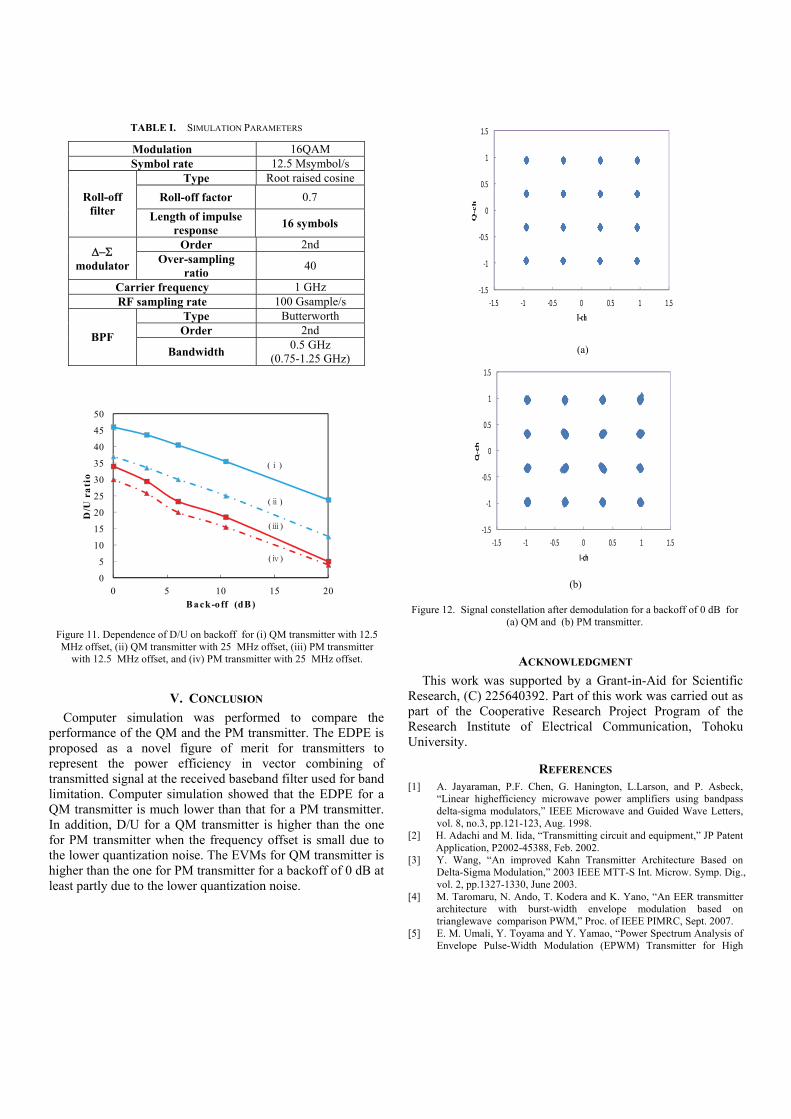
TABLE I. SIMULATION PARAMETERS
Modulation 16QAM Symbol rate 12.5 Msymbol/s
Type Root raised cosineRoll-off factor 0.7 Roll-off
filter Length of impulse response 16 symbols
Order 2nd Δ−Σ
modulator Over-sampling ratio 40
Carrier frequency 1 GHz RF sampling rate 100 Gsample/s
Type Butterworth Order 2nd BPF
Bandwidth 0.5 GHz (0.75-1.25 GHz)
Figure 11. Dependence of D/U on backoff for (i) QM transmitter with 12.5 MHz offset, (ii) QM transmitter with 25 MHz offset, (iii) PM transmitter
with 12.5 MHz offset, and (iv) PM transmitter with 25 MHz offset.
V. CONCLUSION Computer simulation was performed to compare the
performance of the QM and the PM transmitter. The EDPE is proposed as a novel figure of merit for transmitters to represent the power efficiency in vector combining of transmitted signal at the received baseband filter used for band limitation. Computer simulation showed that the EDPE for a QM transmitter is much lower than that for a PM transmitter. In addition, D/U for a QM transmitter is higher than the one for PM transmitter when the frequency offset is small due to the lower quantization noise. The EVMs for QM transmitter is higher than the one for PM transmitter for a backoff of 0 dB at least partly due to the lower quantization noise.
(a)
(b)
Figure 12. Signal constellation after demodulation for a backoff of 0 dB for (a) QM and (b) PM transmitter.
ACKNOWLEDGMENT This work was supported by a Grant-in-Aid for Scientific
Research, (C) 225640392. Part of this work was carried out as part of the Cooperative Research Project Program of the Research Institute of Electrical Communication, Tohoku University.
REFERENCES [1] A. Jayaraman, P.F. Chen, G. Hanington, L.Larson, and P. Asbeck,
“Linear highefficiency microwave power amplifiers using bandpass delta-sigma modulators,” IEEE Microwave and Guided Wave Letters, vol. 8, no.3, pp.121-123, Aug. 1998.
[2] H. Adachi and M. Iida, “Transmitting circuit and equipment,” JP Patent Application, P2002-45388, Feb. 2002.
[3] Y. Wang, “An improved Kahn Transmitter Architecture Based on Delta-Sigma Modulation,” 2003 IEEE MTT-S Int. Microw. Symp. Dig., vol. 2, pp.1327-1330, June 2003.
[4] M. Taromaru, N. Ando, T. Kodera and K. Yano, “An EER transmitter architecture with burst-width envelope modulation based on trianglewave comparison PWM,” Proc. of IEEE PIMRC, Sept. 2007.
[5] E. M. Umali, Y. Toyama and Y. Yamao, “Power Spectrum Analysis of Envelope Pulse-Width Modulation (EPWM) Transmitter for High
0
5
10
15
20
25
30
35
40
45
50
0 5 10 15 20
D/U
rat
io
Back-o ff (dB )
(ⅰ)
(ⅱ)
(ⅲ)
(ⅳ)
‐1.5
‐1
‐0.5
0
0.5
1
1.5
‐1.5 ‐1 ‐0.5 0 0.5 1 1.5
Q‐ch
I‐ch
‐1.5
‐1
‐0.5
0
0.5
1
1.5
‐1.5 ‐1 ‐0.5 0 0.5 1 1.5
Q-c
h
I-ch

Efficiency Amplification of OFDM Signals,” Proc. of IEEE VTC2008-Spring, Singapore, May 2008.
[6] Y. Wang, “A class-s RF amplifier architecture with envelope deltasigma modulation,” IEEE Radio & Wireless Conference, RAWCON2002, pp. 177-179, 2002.
[7] Helaoui, M., Hatami, S., Negra, R., Ghannouchi, F.M., "A Novel Architecture of Delta-Sigma Modulator Enabling All-Digital Multiband Multistandard RF Transmitters Design", IEEE Trans. CAS II: Express Briefs, pp. 1129 – 1133, vol. 55, no.11, Nov. 2008.
[8] M. L. S. Penaloza, G. Baudoin, M.Villegas, “A Cartesian Sigma-Delta Transmitter Architecture”, IEEE Radio and Wireless Symp., pp. 51-54, 2009.
[9] S. Matsumaru, Y. Umeda, O. Takyu, “All-Digital Up-Conversion Type Transmitter with Alternate Generation of I- and Q-Channel,” pp. 288-291, Oct. 2009.
[10] S. Matsumaru, Y. Umeda, O. Takyu, “All-Digital Up-Conversion Type Transmitter with Alternate Generation of I- and Q-Channel,” IEICE Technical Report, vol. 109,no, 434, CAS2009-137, p279, March 2010.
Hironori Izumi received the B.E. degree inElectrical Engineering from TokyoUniversity of Science, Chiba, Japan, in 2011.Since 2011, he is currently pursuing theM.E. degree in Electrical Engineering from Tokyo University of Science. His currentresearch interest is in high power efficiencytransmitter
Michiaki Kojima received the B.E. and M.E. degrees in Electrical Engineering fromTokyo University of Science, Chiba, Japan,in 2010 and 2012, respectively. Since 2012,he joins SOFTBANK MOBILE corporation.
Yohtaro Umeda received the B.S. and M.S.
degrees in physics and the Ph.D. degree inelectrical engineering from the University ofTokyo, Tokyo, Japan, in 1982, 1984, and2000, respectively. In 1984, he joinedNippon Telegraph and Telephone (NTT)Corporation. He moved to Tokyo Universityof Science, Chiba, Japan, as a professor,where he is engaged in the study of high-speed analog circuits for radio and fiber-optic communication systems. Prof. Umedais a member of the IEEE.
Osamu Takyu received the B.E. degree in
Electrical Engineering from TokyoUniversity of science, Chiba, Japan, in 2002 and the M.E. and Ph.D. degree in Open andEnvironmental Systems from KeioUniversity, Yokohama, Japan in 2003 and2006, respectively. From 2003 to 2007, hewas a research associate in the Departmentof Information and Computer Science, KeioUniversity. From 2004 to 2005, he wasvisiting scholar in the school of Electrical
and Information Engineering, University of Sydney. Since2007, he is and assistant professor in the Department of Electrical Engineer, Tokyo University of Science. Dr. takyu is a recipient of young Researcher’s award of IEICE 2010. His current research interests are in wireless communication systems and distributed wireless communication technology. He is a member of IEEE,