understanding vector network analysis product guide · 4 understanding vector network analysis ......
TRANSCRIPT
Product Guide
Understanding VectorNetwork Analysis
2 Understanding Vector Network Analysis
VNA Basics ........................................................................................................................................ 4 Network Analyzers .......................................................................................................................... 6 Scalar Analyzer Comparison .......................................................................................... 7 VNA Fundamentals .......................................................................................................... 7 Network Analyzer Measurements .............................................................................. 13 Measurement Error Correction ................................................................................... 18 Summary .......................................................................................................................... 19 VNA Overview ................................................................................................................................ 20 VNA Architecture ........................................................................................................... 20 Sources ............................................................................................................................ 21 Switches .......................................................................................................................... 27 PIN Diode ........................................................................................................................ 27 Cold FET Switch ............................................................................................................. 28 Directional Devices ........................................................................................................ 30 Down Converters ........................................................................................................... 34 IF Section ........................................................................................................................ 43 System Performance Considerations ........................................................................... 46 Measurement Fundamentals ....................................................................................................... 47 The Reference Plane .......................................................................................................... 47 Introduction to Calibrations ............................................................................................. 48 Linearity .............................................................................................................................. 50 Data Formats ...................................................................................................................... 51 Other Terms of Interest .................................................................................................... 52 System Architecture and Modes of Operation .............................................................. 52 Specifications and Measurement Accuracy ............................................................................... 53 Dynamic Range .................................................................................................................. 54 Compression Level ............................................................................................................ 54 Noise Floor .......................................................................................................................... 55 Trace Noise ......................................................................................................................... 55 Power Range ...................................................................................................................... 56 ALC Power Accuracy and Linearity .................................................................................. 56 Frequency Accuracy and Stability .................................................................................... 56 Harmonics .......................................................................................................................... 56 Raw Directivity .................................................................................................................... 56 Raw Source Match ............................................................................................................. 57 Raw Load Match ................................................................................................................. 57 Residual Directivity .............................................................................................................57 Residual Source Match ...................................................................................................... 57 Residual Load Match ......................................................................................................... 57

3w w w . a n r i t s u . c o m
Residual Reflection Tracking ......................................................................................... 57 Residual Transmission Tracking ..................................................................................... 57 Vector Network Analyzers - VectorStar ....................................................................................... 58 Vector Network Analyzers - ShocklineTM ...................................................................................... 59 Vector Network Analyzers - Handheld ......................................................................................... 60 Summary .......................................................................................................................................... 61 References ....................................................................................................................................... 61

4 Understanding Vector Network Analysis
In this Understanding Guide we will introduce the basic fundamentals of the Vector Network Analyzer (VNA). Specific topics tobecovered includephaseandamplitudemeasurements,scatteringparameters(S-parameters),andthepolarandSmithchartdisplays.
VNA Basics
The VNA measures the magnitude and phase characteristics of networks, amplifiers,components,cables,andantennas.Itcomparestheincidentsignalleavingtheanalyzerwitheitherthesignalthat istransmittedthroughthetestdeviceorthesignalreflectedfromitsinput. Figure 1 and Figure 2 illustrate the different types of measurements that the VNA can perform.
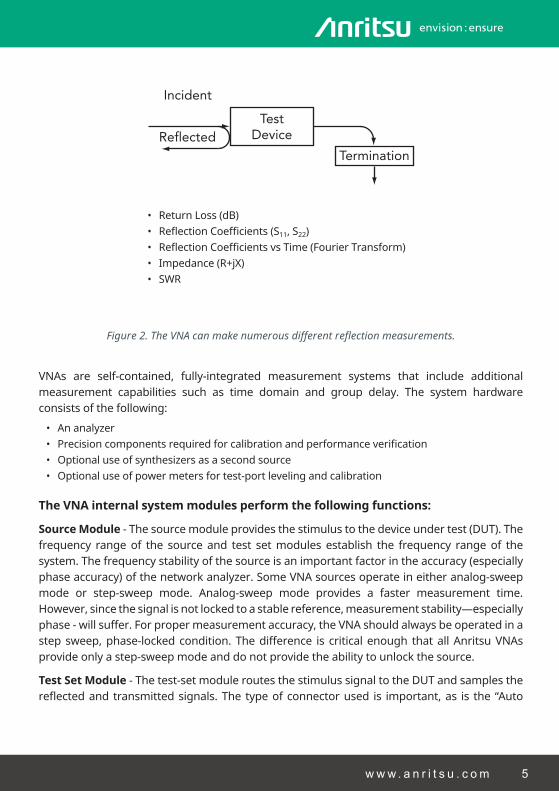
TestDevice
Incident Transmitted
TestDevice
Incident
TerminationReflected
• Gain (dB)• Insertion Loss (dB)• Insertion Phase (degrees)• TransmissionCoefficients(S21,S12)• Complex Transmission Components (Magnitude and
Phase)• Electrical Length (m)• Electrical Delay (s)• Deviation from Linear Phase (degrees)• Group Delay (s)
Figure 1. The VNA can make a wide range of transmission measurements.
5w w w . a n r i t s u . c o m
TestDevice
Incident Transmitted
TestDevice
Incident
TerminationReflected
• Return Loss (dB)• ReflectionCoefficients(S11,S22)• ReflectionCoefficientsvsTime(FourierTransform)• Impedance (R+jX)• SWR
Figure 2. The VNA can make numerous different reflection measurements.
VNAs are self-contained, fully-integrated measurement systems that include additionalmeasurement capabilities such as time domain and group delay. The system hardware consists of the following:
• An analyzer• Precisioncomponentsrequiredforcalibrationandperformanceverification• Optional use of synthesizers as a second source• Optional use of power meters for test-port leveling and calibration
The VNA internal system modules perform the following functions:
Source Module - The source module provides the stimulus to the device under test (DUT). The frequency range of the source and test set modules establish the frequency range of the system. The frequency stability of the source is an important factor in the accuracy (especially phase accuracy) of the network analyzer. Some VNA sources operate in either analog-sweep mode or step-sweep mode. Analog-sweep mode provides a faster measurement time. However,sincethesignalisnotlockedtoastablereference,measurementstability—especiallyphase-willsuffer.Forpropermeasurementaccuracy,theVNAshouldalwaysbeoperatedinastepsweep,phase-lockedcondition.Thedifference is criticalenough thatallAnritsuVNAsprovide only a step-sweep mode and do not provide the ability to unlock the source.
Test Set Module - The test-set module routes the stimulus signal to the DUT and samples the reflectedandtransmittedsignals.The typeofconnectorused is important,as is the “Auto
6 Understanding Vector Network Analysis
Reversing” feature. Auto Reversing means that the stimulus signal is applied in both the forward and reverse directions. The direction is reversed automatically. This saves the engineer from having to physically reverse the test device to measure all four S-parameters. It also increases accuracy by reducing connector repeatability errors. Frequency conversion to the Intermediate Frequency (IF) range also occurs in the test-set module.
Analyzer Module - The analyzer module receives and interprets the IF signal for phase and magnitude data. It then displays the results of this analysis on a high-resolution display screen. ThisdisplaycanshowallfourS-parameterssimultaneously,aswellasavarietyofotherformsofdisplayed informationsuchasgroupdelay, timeanddistance,andcomplex impedanceinformation.Inadditiontotheinstalleddisplay,theengineercanalsoviewthemeasurementresults on an external monitor.
Network Analyzers
This discussion of networks analyzers begins with a subject familiar to most analyzer users: scalarnetworkanalysis.Aftershowingcomparisons,thefundamentalsofnetworkanalyzerterminology and techniques will be presented. This discussion serves as an introduction to topics presented in greater detail later in this chapter and will touch on the concepts of:
• Reference delay• S-Parameters: what they are and how they are displayed• Complex impedance and Smith charts
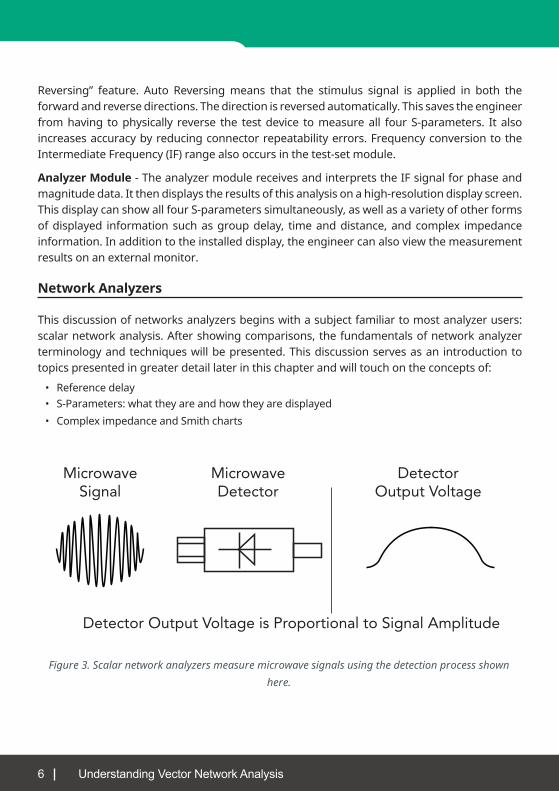
Figure 3. Scalar network analyzers measure microwave signals using the detection process shown here.
MicrowaveSignal
MicrowaveDetector
DetectorOutput Voltage
Detector Output Voltage is Proportional to Signal Amplitude
7w w w . a n r i t s u . c o m
Scalar Analyzer Comparison
VNAsdoeverythingthatscalaranalyzersdo,plustheyaddtheabilitytomeasurethephasecharacteristics of microwave devices over a greater dynamic range and with more accuracy. If all a VNAaddedwas the ability tomeasurephase characteristics, its usefulnesswouldbelimited. While phase measurements are important, the availability of phase informationprovidesthepotentialformanynewcomplex-measurementfeatures,includingSmithcharts,time domain and group delay. Phase information also allows greater accuracy through vector-error correction of the instrument’s own mismatches so that the instrument’s own uncorrected characteristicsdonotinfluencetheactualDUTresponse.
Now consider the scalar network analyzer (SNA), an instrument thatmeasuresmicrowavesignals by converting them to a DC voltage using a diode detector (Figure 3). This DC voltage is proportional to themagnitude of the incoming signal. The detection process, however,ignores any information regarding the microwave signal’s phase. Also, a detector is abroadband-detectiondevicewhichmeansthatallfrequencies,thefundamental,harmonics,sub-harmonics, and any other spurious signals within the bandwidth of the detector, aredetectedandsimultaneouslydisplayedasonesignal.Thismayaddsignificanterrortoboththe absolute and relative measurements.
In a VNA, information regarding both themagnitude and phase of amicrowave signal isextracted.Whiletherearedifferentwaystoperformthismeasurement,themethodemployedby the Anritsu series of VNAs is to down-convert the signal to a lower IF in a process called harmonic sampling. This signal can then be measured directly by a tuned receiver. The tuned receiver approach gives the system greater dynamic range due to its variable IF-filterbandwidth control. The system is alsomuch less sensitive to interfering signals, includingharmonics.
VNA Fundamentals
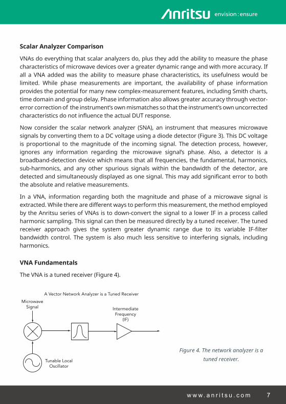
The VNA is a tuned receiver (Figure 4).
MicrowaveSignal
Tunable LocalOscillator
IntermediateFrequency
(IF)
A Vector Network Analyzer is a Tuned Receiver
Figure 4. The network analyzer is a tuned receiver.

8 Understanding Vector Network Analysis
The microwave signal is down converted into the passband of the IF. To measure the phase of thissignalasitpassesthroughtheDUT,areferenceisneededforcomparison.Ifthephaseofasignalis90degrees,itis90degreesdifferentfromthereferencesignal(Figure5).TheVNAreadsthisas–90degrees,sincethetestsignalisdelayedby90degreeswithrespecttothereference signal. The phase reference can be obtained by splitting off a portion of the microwave signal before the measurement (Figure 6).
Thephaseofthemicrowavesignal,afterithaspassedthroughtheDUT,isthencomparedwiththe reference signal. A network-analyzer test set automatically samples the reference signal so no external hardware is needed.
Phase Measurement
Time
Reference Signal
Test Signal
Figure 5. Shown here are signals with a 90-degree phase difference.
Figure 6. Splitting the microwave signal to obtain the phase reference.
MicrowaveSource
ReferenceSignal
TestSignal
Splitter
PhaseDetector
DUT

9w w w . a n r i t s u . c o m
Consider the case where the DUT is removed and a length of transmission line is substituted (Figure 7). Note that the path length of the test signal is longer than that of the reference signal. How does this affect the measurement?
Toanswerthisquestion,assumethatameasurementisbeingmadeat1GHzandthatthedifference in path length between the two signals is exactly 1 wavelength. This means that the test signal lags behind the reference signal by 360 degrees (Figure 8). It is impossible to tell the difference between one sine wave maxima and the next because they are all identical. Consequently,thenetworkanalyzermeasuresaphasedifferenceof0degrees.
MicrowaveSource
ReferenceSignal
TestSignal
Splitter
PhaseDetector
LongPath
Length
Figure 7. Pictured here is the case of a split signal where a length of line replaces the DUT.
MicrowaveSource
ReferenceSignal
TestSignal
Splitter
PhaseDetector
Longer byOne Wavelength
Length (360 Degrees)
Figure 8. Depicted here is the case for a split signal where the path length differs by exactly one wave-length.

10 Understanding Vector Network Analysis
Now,considerthatthissamemeasurementismadeat1.1GHz.Sincethefrequencyishigherby10percent,thewavelengthofthesignalisshorterby10percent.Thetest-signalpathlengthis now 0.1 wavelength longer than that of the reference signal (Figure 9). This test signal is: 1.1 x 360 = 396 degrees. This is 36 degrees different from the phase measurement at 1 GHz. The network analyzer displays this phase difference as –36 degrees. The test signal at 1.1 GHz is delayed by 36 degrees more than the test signal at 1 GHz.
MicrowaveSource
ReferenceSignal
TestSignal
Splitter
PhaseDetector
Same Path Length ButWavelength is Now Shorter
1.1 Wavelengths = 396 Degrees
Figure 9. Depicted here is the case for a split signal where the path length differs by the same path length, but the wavelength is now shorter. Note that 1.1 wavelengths = 396 degrees.
Mea
sure
d P
hase
+180°
+90°
+0°
-90°
-180°
1.1 1.2 1.3 1.4 Frequency in GHz
Figure 10. This graphic depicts electrical delay.

11w w w . a n r i t s u . c o m
Ameasurement frequency of 1.2 GHz produces a reading of –72 degrees, while 1.3 GHzproduces a reading of –108 degrees (Figure 10). There is an electrical delay between the reference and test signals. This delay is commonly referred to in the industry as the reference delay.Itisalsocalledphasedelay.Inoldernetworkanalyzers,thelengthofthereferencepathhadtobeconstantlyadjusted—relativetothetestpath—tomakeanappropriatemeasurementof phase versus frequency.
Tomeasure phase on a DUT, this phase-change versus frequency due to changes in theelectrical length must be removed. This allows the actual phase characteristics to be viewed. These characteristics may be much smaller than the phase change due to electrical-length difference.
MicrowaveSource
ReferenceSignal
TestSignal
Splitter
PhaseDetector
Both LineLengths
Now Equal
1.1 Wavelengths = 396 Degrees
Figure 11. This graphic depicts a split signal where paths are equal in length.

12 Understanding Vector Network Analysis
The second approach involves handling the path-length difference in software. Figure 12 displays the phase versus frequency of a device. This device has different effects on the output phase at different frequencies. Because of these differences, the phase response is notperfectly linear. This phase deviation can be easily detected by compensating for the linear phase.Becausethesizeofthephasedifferenceincreaseslinearlywithfrequency,thephasedisplaycanbemodifiedtoeliminatethisdelay.
Anritsu VNAs offer automatic reference-delay compensation with the push of a button. Figure 13 shows the resultant measurement when the path length is compensated.
Mea
sure
d P
hase
+180°
+90°
+0°
-90°
-180°
Frequency in GHz1.1 1.2 1.3 1.4
Subtract LinearPhase FromMeasured Phase
Figure 12. Here phase difference increases linearly with frequency.
Res
ulta
nt P
hase
+180°
+90°
+0°
-90°
-180°
Frequency in GHz1.1 1.2 1.3 1.4
Figure 13. Shown here is the resultant phase with path length.
13w w w . a n r i t s u . c o m
Network Analyzer Measurements
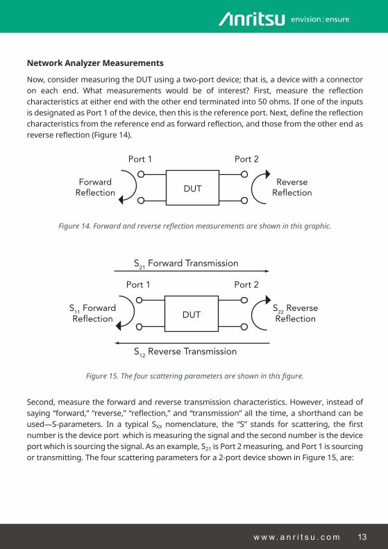
Now,considermeasuringtheDUTusingatwo-portdevice;thatis,adevicewithaconnectoron each end. What measurements would be of interest? First, measure the reflectioncharacteristics at either end with the other end terminated into 50 ohms. If one of the inputs isdesignatedasPort1ofthedevice,thenthisisthereferenceport.Next,definethereflectioncharacteristicsfromthereferenceendasforwardreflection,andthosefromtheotherendasreversereflection(Figure14).
Port 1
ReverseReflectionDUT
Port 2
ForwardReflection
Figure 14. Forward and reverse reflection measurements are shown in this graphic.
Port 1
S22 ReverseReflectionDUT
Port 2
S11 ForwardReflection
S21 Forward Transmission
S12 Reverse Transmission
Figure 15. The four scattering parameters are shown in this figure.
Second,measuretheforwardandreversetransmissioncharacteristics.However,insteadofsaying“forward,”“reverse,”“reflection,”and“transmission”allthetime,ashorthandcanbeused—S-parameters. In a typical SXX nomenclature, the “S” stands for scattering, the firstnumber is the device port which is measuring the signal and the second number is the device portwhichissourcingthesignal.Asanexample,S21isPort2measuring,andPort1issourcingortransmitting.Thefourscatteringparametersfora2-portdeviceshowninFigure15,are:

14 Understanding Vector Network Analysis
• S11forwardreflection• S21 forward transmission• S22reversereflection• S12 reverse transmission
S-parameters can be displayed in many ways. An S-parameter consists of a magnitude and a phase.ThemagnitudeisdisplayedindB,justliketheSNA,andiscalledthelogmagnitude.Another method of magnitude display is to use units instead of dB. When displaying magnitude inunits,thevalueofthereflectedortransmittedsignalwillbebetween0and1relativetothereference.
Phasecanbedisplayedas“linearphase”(Figure16).Asdiscussedearlier,it’simpossibletotellthedifferencebetweenonecycleandthenext.Therefore,aftergoingthrough360degrees,the engineer ends up back at the beginning. Displaying the measurement from –180 to +180 degrees is a more common approach. This method keeps the display discontinuity removed from the important 0 degree area which is used as the phase reference.
Polar Display
+180º 0º
+90º
-90º
Pha
se
Frequency-180º
0º
+180º
Figure 16. This waveform depicts linear phase with frequency.
Figure 17. An example of a polar display.

15w w w . a n r i t s u . c o m
There are several ways in which all the information can be displayed on one trace. One method is a polar display (Figure 17). In this display, the radial parameter (e.g., distance from thecenter)ismagnitude,whiletherotationaroundthecircleisphase.Polardisplaysaresometimesused to view transmissionmeasurements, especially on cascaded devices (e.g., devices inseries). The transmission result is the addition of the phase and log magnitude (dB) information of each device’s polar display.
Aspreviouslydiscussed,thesignalreflectedfromaDUThasbothmagnitudeandphase.Thisis because the impedance of the device has both a resistive and a reactive term of the form R+jX,whereRistherealorresistivetermandXistheimaginaryorreactiveterm.Thej,whichissometimesdenotedasi,isanimaginarynumberandisthesquarerootof–1.IfXispositive,theimpedanceisinductive.IfXisnegative,theimpedanceiscapacitive.
Inductive50Ω
Capacitive
Figure 18. An example of a Smith chart.
The size and polarity of the reactive component X is important in impedance matching. The best match to a complex impedance is the complex conjugate. This complex sounding term simplymeansanimpedancewiththesamevalueofRandX,butwithXofoppositepolarity.This term is best analyzed using a Smith chart which is a plot of R and X (Figure 18). Displaying alloftheinformationonasingleS-parameterrequiresoneortwotraces,dependingontheformatdesired.AverycommonrequirementistoviewforwardreflectiononaSmithchart(onetrace),whileobservingforwardtransmissioninlogmagnitudeandphase(twotraces).Inaddition,itisalsoveryhelpfultosimultaneouslydisplayotherdisplayssuchasTimeDomainand Group Delay while monitoring the S11 and S21 parameters. This requires a VNA with a complex display capability such as the any of the Anritsu benchtop VNAs.

16 Understanding Vector Network Analysis
Figure 19. Shown here is the VectorStar multiple channel and multiple trace display.
Figure 20. The VectorStar display of a group delay measurement of a wireless communication filter.
17w w w . a n r i t s u . c o m
TheVectorStarandShockLineseriesVNAshavetheabilitytoconfigureonetosixteenchannels.EachchannelcanthoughtofasanindependentVNA.Therefore,achannelintheVectorStarorShocklinecanbeconfiguredforaspecificfrequencyrange,calibrationtype,powerlevel,andIF-filter bandwidth setting. Additional channels can be configuredwithin the VNA to helpfacilitatetestinginmultiplesetupparameters,uptothe16channelsavailable.TheVectorStarorShocklinecanalsobeconfiguredtodisplayalloftheactivechannelsinapatternthatismostuseful to the user.
Withmultiplechannelsconfigured,theAnritsuVNAsequentiallysweepsfromonecalibratedsetupandmeasurementconditiontothenext.Eachofthechanneldisplayscanbeconfiguredtoacceptupto16traces.Allofthetracesineachchannelcanlikewisebeconfiguredforthemost beneficial display pattern. Finally, each of these traces can be configured for anappropriatedisplay,dependingonthetypeofdatabeingdisplayed(Figure19).Forinstance,Trace 6 can be set up to provide S11performanceofthedevicedisplayedonaSmithchart,Trace 7 can be set up for S11 withaTimeDomaindisplay,andTrace12canbesetupforanS21 display on a Log Magnitude and Phase graph.
Another important parameter that can be measured with phase information is group delay (Figure 20). In linear devices, the phase change through theDUT is linear-with-frequency.Thus,doublingthefrequencyalsodoublesthephasechange.An importantmeasurement,especiallyforcommunicationssystemusers,istherateofchange-of-phaseversusfrequency(e.g.,groupdelay).Iftherateofphase-changeversusfrequencyisnotconstant,theDUTisnonlinear. This nonlinearity can create distortion in communications systems.
18 Understanding Vector Network Analysis
Measurement Error Correction
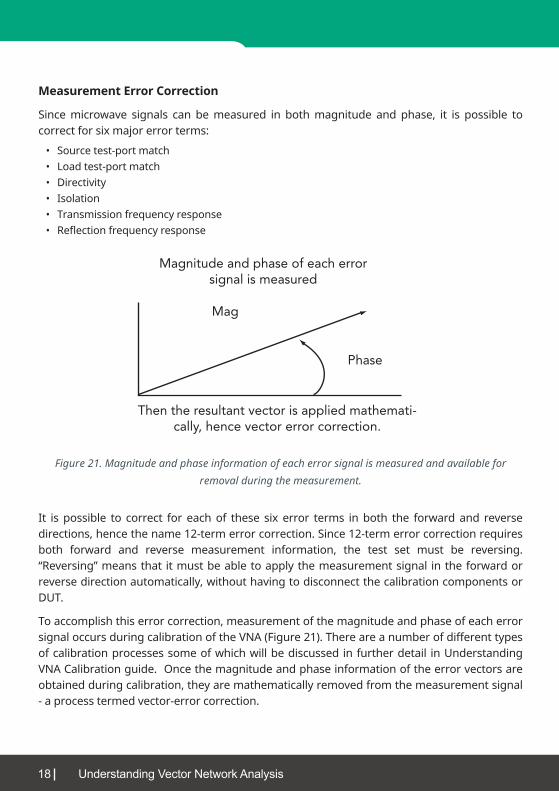
Sincemicrowave signals can bemeasured in bothmagnitude and phase, it is possible tocorrect for six major error terms:
• Source test-port match• Load test-port match• Directivity• Isolation• Transmission frequency response• Reflectionfrequencyresponse
Magnitude and phase of each error signal is measured
Then the resultant vector is applied mathemati-cally, hence vector error correction.
Mag
Phase
Figure 21. Magnitude and phase information of each error signal is measured and available for removal during the measurement.
It is possible to correct for each of these six error terms in both the forward and reverse directions,hencethename12-termerrorcorrection.Since12-termerrorcorrectionrequiresboth forward and reverse measurement information, the test set must be reversing.“Reversing”meansthat itmustbeabletoapplythemeasurementsignal intheforwardorreversedirectionautomatically,withouthavingtodisconnectthecalibrationcomponentsorDUT.
Toaccomplishthiserrorcorrection,measurementofthemagnitudeandphaseofeacherrorsignal occurs during calibration of the VNA (Figure 21). There are a number of different types of calibration processes some of which will be discussed in further detail in Understanding VNA Calibration guide. Once the magnitude and phase information of the error vectors are obtainedduringcalibration,theyaremathematicallyremovedfromthemeasurementsignal- a process termed vector-error correction.

19w w w . a n r i t s u . c o m
Summary
ComparedtotheSNA,theVNAisamuchmorepowerfulanalyzer.ThemajordifferenceisthattheVNAaddstheabilitytomeasurephase,aswellasamplitude.Withphasemeasurementscome S-parameters, which are a shorthand method for identifying forward and reversetransmissionandreflectioncharacteristics.Theabilitytomeasurephaseintroducestwonewdisplays,polarandSmithchart.Italsoaddsvector-errorcorrectiontothemeasurementtrace.Withvector-errorcorrection,errorsintroducedbythemeasurementsystemarecompensatedfor and measurement uncertainty is minimized. Phase measurements also add the capability formeasuringgroupdelay,whichistherateofchange-of-phaseversusfrequency(e.g.,groupdelay).Allinall,usinganetworkanalyzerprovidesforamorecompleteanalysisofanytestdevice.

20 Understanding Vector Network Analysis
VNA Overview
This section isdesigned to introduce the reader to the fundamentalsofVNAarchitecture,measurements,specifications,andperformance.Init,themajorfunctionalanalogblocksinaRF/microwaveVNAareexamined,alongwith the currentandpast technologieswhichareused in these blocks. This content will serve as the foundation on which more advanced concepts will later be developed.
VNA Architecture
Initsmostbasicform,theobjectiveofaVNAistocaptureS-parameterdata.MostVNA’stodayare designed for use with 50 ohm impedance DUT’s. The basic requirements for capturing S-parameter data include:
• Oneormoresignalsourceswith,atminimum,controllablefrequencyandasufficiently-cleanspectral tone for making a measurement. Sources with controlled power are preferred.
• Directional devices - whether physically or computationally directional - for separating incident andreflectedwavesattheports.
• AmeansofswitchingRFsignalswhentherearefewersourcesthanports,oreithermoreorfewer receivers than ports.
• Oneormorereceivers,usuallywithdownconverters,totakeincidentandreflectedwavesdown to some convenient IF for processing.
• An IF section and digitizer to transform the converted wave amplitudes into a useful form for computation.
Source
ReferenceSignal
IFSection
DownConverter
DownConverter
DownConverter
DownConverter
LO
Port 1
Port 2
Figure 22. Shown here is one possible VNA block diagram, illustrating the key blocks to be discussed in this section.

21w w w . a n r i t s u . c o m
AsimplifiedblockdiagramofacommonVNAisshowninFigure22.Manyvariationsonthisstructure are possible. For example, one source could be used for each port instead ofswitchingasinglesourcebetweentwoports,orthecouplingdevicescouldberepositioned.Thediagram therefore, is simply intended topointout that the functions listedabovearegenerally all present in one form or another and play a role in overall system performance.
Sources
Itmightbe tempting toview theVNAsourcesomewhatsimplistically—asasynthesizerorsweeper somehow synchronized with a local oscillator (LO) to produce the desired transceiver behavior.Inpractice,therearemanycompetingdemandsonperformanceandconsequently,thesource isbasedonacomplexseriesofdecisions.Speed, forexample, isoften timesacriticalcomponentofthemodernVNA,whilespectralpurityistypicallynotascriticalsincetheengineer knows what frequency he/she is trying to measure. The engineer cannot deviate too far,however,becausethephasenoiseofthesourcesinvolvedaffectstracenoise,spurringthesourcestoproduceundesiredreceiverresponseswhichimpactsnetdynamicrange.Similarly,the source is impacted by the desired application. Because the VNA may also be used to make mixer measurements and multi-tone analysis, any architectural choices pertaining to thesourcebecomemoreconstrained(e.g.,spectralpurityagainbecomesimportant).
Figure 23. A generic source block diagram illustrates some of the architectural choices to be made by the engineer.
A simplistic block diagram of a source is shown in Figure 23. The diagram is extremely general since there are many possible structures. Note that if large portions of the source are digitally generatedthisdiagramisnotaccurate.Inthediagram,thereferencecomesfromthesystem’scrystaloscillatororsynthesizer,whilefeedbackcomesfromeitherthetunableoscillator(e.g.,aclassicalphase-lockedloop(PLL))orelsewhereinthesystem.Theloopfiltermaybestaticor
Reference
Feedback
PhaseDetector
Loop Filter
ControlInputs
Tunable Oscillatorof Some Technology
Mixing, Mult. Division,
Modulation
LevelControl
22 Understanding Vector Network Analysis
of dynamic bandwidth and gain. The oscillator output may be frequency-converted or modulated.Insomecases,thesourcemaynotevenbelocked—althoughthisdecisionincursan accuracy penalty.
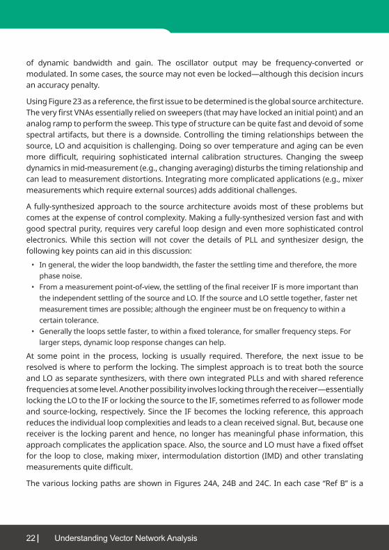
UsingFigure23asareference,thefirstissuetobedeterminedistheglobalsourcearchitecture.TheveryfirstVNAsessentiallyreliedonsweepers(thatmayhavelockedaninitialpoint)andananalog ramp to perform the sweep. This type of structure can be quite fast and devoid of some spectralartifacts,butthereisadownside.Controllingthetimingrelationshipsbetweenthesource,LOandacquisitionischallenging.Doingsoovertemperatureandagingcanbeevenmore difficult, requiring sophisticated internal calibration structures. Changing the sweepdynamicsinmid-measurement(e.g.,changingaveraging)disturbsthetimingrelationshipandcanleadtomeasurementdistortions.Integratingmorecomplicatedapplications(e.g.,mixermeasurements which require external sources) adds additional challenges.
A fully-synthesized approach to the source architecture avoids most of these problems but comes at the expense of control complexity. Making a fully-synthesized version fast and with goodspectralpurity,requiresverycarefulloopdesignandevenmoresophisticatedcontrolelectronics.While this sectionwill not cover thedetailsofPLLand synthesizerdesign, thefollowing key points can aid in this discussion:
• Ingeneral,thewidertheloopbandwidth,thefasterthesettlingtimeandtherefore,themorephase noise.
• Fromameasurementpoint-of-view,thesettlingofthefinalreceiverIFismoreimportantthantheindependentsettlingofthesourceandLO.IfthesourceandLOsettletogether,fasternetmeasurementtimesarepossible;althoughtheengineermustbeonfrequencytowithinacertain tolerance.
• Generallytheloopssettlefaster,towithinafixedtolerance,forsmallerfrequencysteps.Forlargersteps,dynamicloopresponsechangescanhelp.
At some point in the process, locking is usually required. Therefore, the next issue to beresolved is where to perform the locking. The simplest approach is to treat both the source andLOasseparatesynthesizers,withthereownintegratedPLLsandwithsharedreferencefrequenciesatsomelevel.Anotherpossibilityinvolveslockingthroughthereceiver—essentiallylockingtheLOtotheIForlockingthesourcetotheIF,sometimesreferredtoasfollowermodeandsource-locking,respectively.SincetheIFbecomesthe lockingreference,thisapproachreducestheindividualloopcomplexitiesandleadstoacleanreceivedsignal.But,becauseonereceiveristhelockingparentandhence,nolongerhasmeaningfulphaseinformation,thisapproachcomplicatestheapplicationspace.Also,thesourceandLOmusthaveafixedoffsetforthe looptoclose,makingmixer, intermodulationdistortion(IMD)andothertranslatingmeasurementsquitedifficult.
ThevariouslockingpathsareshowninFigures24A,24Band24C.Ineachcase“RefB”isa

23w w w . a n r i t s u . c o m
secondary reference usually derived from the main system frequency reference (reference A). Insomecases,thetworeferencescanbethesamesignalbutthisisnotnecessaryorcommon.
Source
LO
Test Set and DUT
Down Converter
IF to A/DConverters
Reference
PLLInputs
PLLInputs
Figure 24A. This diagram illustrates a fully-synthesized architecture where the source and LO PLLs are semi-self-contained. The source and PLLs may be linked together at any level and even derived from
each other, but they do not involve the system receiver.
Many decisions have to be made with regard to the individual PLLs. While most of these decisionsarebeyondthescopeofthissection,afewcommentsareworthnoting.Historically,Yttrium-iron-garnet (YIG) oscillators have been used as the source in source-locking architectures like the one shown in Figure 24B. While the phase noise of such oscillators is quitegood,theytendtobeslow(atleastinbroadbandconfigurations).Morerecently,VNAshaveemergedinwhichallsourcesarebasedonvaractor-tuned,voltage-controlledoscillators(VCOs) and can therefore tune much faster. The trade-off is degraded phase noise at offsets thatismuchlargerthantheloopbandwidth.AsVCOtechnologyimproves,thesedifferenceshave been shrinking.
The fine-tuning structure of these loops has also changed in recent history. Fractional-Nstructures are verypopular and canofferfine-tuning resolutionwithdecent spurious andnoise performance. Wide-bandwidth, direct-digital synthesizers have also become morecommon recently, thanks to their ever-improving spurious performance. The fine-tuningcapabilities of such structures are needed since the VNA tuning resolution must typically be on the order of 1 Hz.

24 Understanding Vector Network Analysis
Figure 24B. A source-locking architecture is shown here. The source is locked to the IF through the down converter. Since the loop tries to maintain a clean IF, any noise on the LO is transferred, in a
canceling fashion, to the source.
Figure 24C. A follower architecture is shown here. In this case, the LO is locked to the IF. Since the loop tries to keep the IF clean, noise on the source is transferred, in a canceling fashion, to the LO.
Source
LO
Test Set and DUT
Down Converter
IF to A/DConverters
PLLInputs
PLLInputs
Reference
Reference A
Reference B
Source
LO
Test Set and DUT
Down Converter
IF to A/DConverters
Reference A
PLLInputs
PLLInputs
Reference B
25w w w . a n r i t s u . c o m
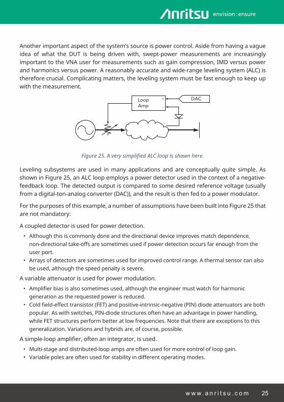
Another important aspect of the system’s source is power control. Aside from having a vague idea of what the DUT is being driven with, swept-power measurements are increasinglyimportanttotheVNAuserformeasurementssuchasgaincompression,IMDversuspowerand harmonics versus power. A reasonably accurate and wide-range leveling system (ALC) is thereforecrucial.Complicatingmatters,thelevelingsystemmustbefastenoughtokeepupwith the measurement.
Loop Amp
+
-
DAC
Figure 25. A very simplified ALC loop is shown here.
Leveling subsystems are used in many applications and are conceptually quite simple. As showninFigure25,anALCloopemploysapowerdetectorusedinthecontextofanegative-feedback loop. The detected output is compared to some desired reference voltage (usually fromadigital-ton-analogconverter(DAC)),andtheresultisthenfedtoapowermodulator.
Forthepurposesofthisexample,anumberofassumptionshavebeenbuiltintoFigure25thatare not mandatory:
A coupled detector is used for power detection.
• Althoughthisiscommonlydoneandthedirectionaldeviceimprovesmatchdependence,non-directional take-offs are sometimes used if power detection occurs far enough from the user port.
• Arrays of detectors are sometimes used for improved control range. A thermal sensor can also beused,althoughthespeedpenaltyissevere.
A variable attenuator is used for power modulation.
• Amplifierbiasisalsosometimesused,althoughtheengineermustwatchforharmonicgeneration as the requested power is reduced.
• Coldfield-effecttransistor(FET)andpositive-intrinsic-negative(PIN)diodeattenuatorsarebothpopular.Aswithswitches,PIN-diodestructuresoftenhaveanadvantageinpowerhandling,while FET structures perform better at low frequencies. Note that there are exceptions to this generalization.Variationsandhybridsare,ofcourse,possible.
Asimple-loopamplifier,oftenanintegrator,isused.
• Multi-stage and distributed-loop amps are often used for more control of loop gain.• Variable poles are often used for stability in different operating modes.
26 Understanding Vector Network Analysis
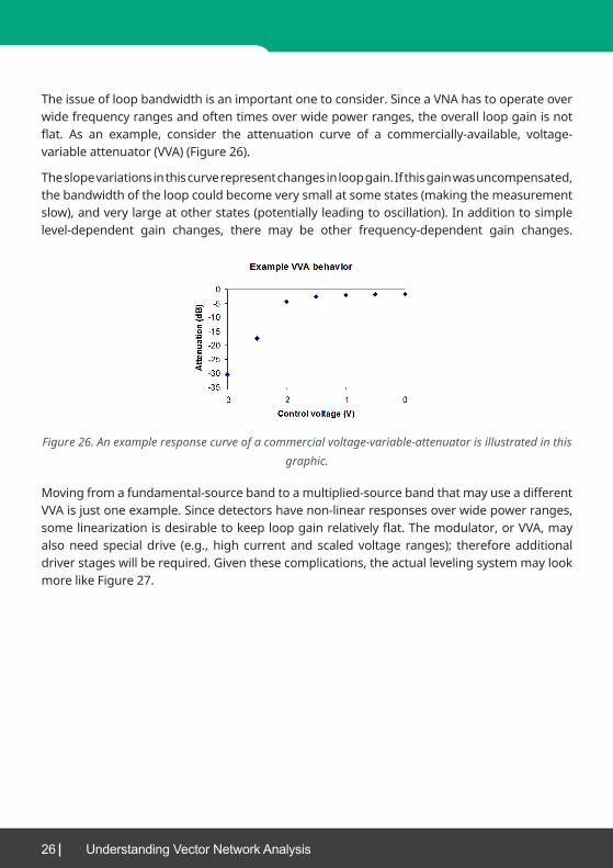
The issue of loop bandwidth is an important one to consider. Since a VNA has to operate over widefrequencyrangesandoftentimesoverwidepowerranges,theoverallloopgainisnotflat. As an example, consider the attenuation curve of a commercially-available, voltage-variable attenuator (VVA) (Figure 26).
Theslopevariationsinthiscurverepresentchangesinloopgain.Ifthisgainwasuncompensated,the bandwidth of the loop could become very small at some states (making the measurement slow),andverylargeatotherstates(potentiallyleadingtooscillation).Inadditiontosimplelevel-dependent gain changes, there may be other frequency-dependent gain changes.
Moving from a fundamental-source band to a multiplied-source band that may use a different VVAisjustoneexample.Sincedetectorshavenon-linearresponsesoverwidepowerranges,somelinearizationisdesirabletokeeploopgainrelativelyflat.Themodulator,orVVA,mayalsoneed specialdrive (e.g., high current and scaled voltage ranges); thereforeadditionaldriverstageswillberequired.Giventhesecomplications,theactuallevelingsystemmaylookmore like Figure 27.
Figure 26. An example response curve of a commercial voltage-variable-attenuator is illustrated in this graphic.
27w w w . a n r i t s u . c o m
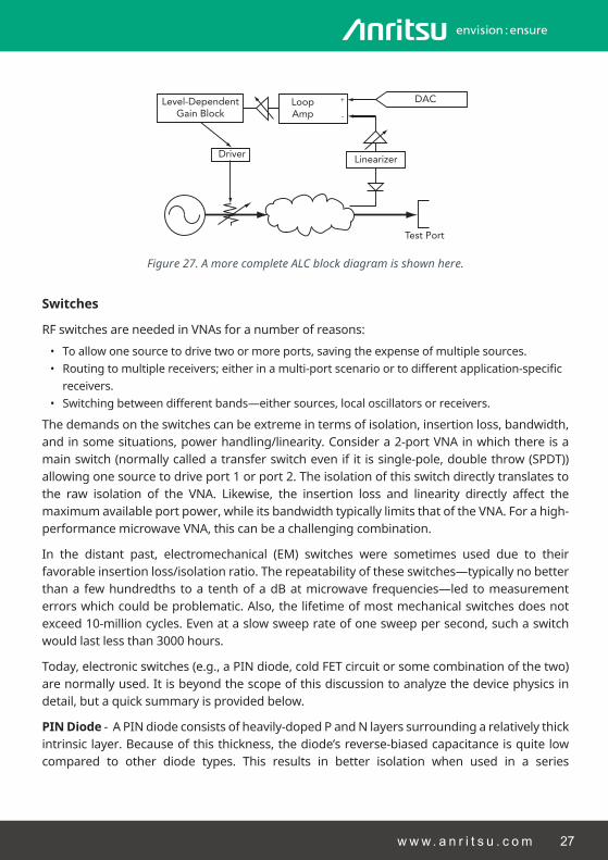
Figure 27. A more complete ALC block diagram is shown here.
Switches
RF switches are needed in VNAs for a number of reasons:
• Toallowonesourcetodrivetwoormoreports,savingtheexpenseofmultiplesources.• Routingtomultiplereceivers;eitherinamulti-portscenarioortodifferentapplication-specific
receivers.• Switchingbetweendifferentbands—eithersources,localoscillatorsorreceivers.
Thedemandsontheswitchescanbeextremeintermsofisolation,insertionloss,bandwidth,andinsomesituations,powerhandling/linearity.Considera2-portVNAinwhichthereisamainswitch(normallycalledatransferswitchevenif it issingle-pole,doublethrow(SPDT))allowing one source to drive port 1 or port 2. The isolation of this switch directly translates to the raw isolation of the VNA. Likewise, the insertion loss and linearity directly affect themaximumavailableportpower,whileitsbandwidthtypicallylimitsthatoftheVNA.Forahigh-performancemicrowaveVNA,thiscanbeachallengingcombination.
In the distant past, electromechanical (EM) switches were sometimes used due to theirfavorableinsertionloss/isolationratio.Therepeatabilityoftheseswitches—typicallynobetterthana fewhundredths toa tenthofadBatmicrowave frequencies—led tomeasurementerrorswhichcouldbeproblematic.Also,thelifetimeofmostmechanicalswitchesdoesnotexceed10-millioncycles.Evenataslowsweeprateofonesweeppersecond,suchaswitchwould last less than 3000 hours.
Today,electronicswitches(e.g.,aPINdiode,coldFETcircuitorsomecombinationofthetwo)are normally used. It is beyond the scope of this discussion to analyze the device physics in detail,butaquicksummaryisprovidedbelow.
PIN Diode - A PIN diode consists of heavily-doped P and N layers surrounding a relatively thick intrinsiclayer.Becauseofthisthickness,thediode’sreverse-biasedcapacitanceisquitelowcompared to other diode types. This results in better isolation when used in a series
Loop Amp
+
-
DAC
Driver Linearizer
Level-DependentGain Block
Test Port

28 Understanding Vector Network Analysis
constructionandless insertion loss inashunttopology.Whenforwardbiased,carriersareinjected into the intrinsic layer but do not recombine immediately. This causes complications at lower frequencies since the RF frequency can be on the same scale as the recombination rate and distortion occurs.
Cold FET Switch - A typical cold FET switch is just that: a Metal Epitaxial Semiconductor Field Effect Transistor (MESFET) or similar structure setup with no drain bias. When the gate is biased strongly negative, no carriers are available in the channel and the device providesreasonableisolationinaseriessense.LikethePINdiode,theoffcapacitance(draintosource)of the cold FET is fairly low due to the geometry. Shunt-topology insertion losses are therefore low as well, although they are typically worse than with a PIN structure. The elevatedcapacitance can be mitigated by embedding the switch in a transmission-line structure. When thegateisneargroundpotential,carriersareavailableinthechannel,alongwitharelatively-lowseriesresistance.UnlikethePINdiode,therecombinationtimeremainsfastsotherearefewlow-frequencyeffects.Sincetheengineerisusuallyoperatingagainsta0-biaslimit,therecan be linearity issues.
Figure 28. SPST topologies include series, shunt and series-shunt.
The common single-pole-single-throw (SPST) topologies are shown in Figure 28. It is not uncommon to have the series-shunt pair contained within a single die or package.
Whichevertechnology,orcombinationoftechnologies,ischosen,theissueofswitchtopologyiscritical.Forsimpleapplicationsrequiring low isolation,asingleseries-shuntelementperarmmaybeappropriate(Figure29A).Insomecases,asingleelementmayevenbeused,butsevere match implications on a multi-throw switch are possible. When high levels of isolation arerequired,moreelementsareoftenusedperpath(Figure29B).Therearemanychoicestheengineer can make about the combinations of elements. Here are a few tips:

29w w w . a n r i t s u . c o m
Serieselementsgenerallybecomelesseffectiveathighermicrowavefrequencies,requiringmore shunt elements in that frequency range.
• Sometimes series-shunt pairs are available as a single die or cell and are often convenient to bias that way.
• Properallocationforbiasinginductorsmustbemade,primarilyforPINswitches.Theirlayoutiscriticalsinceabove50GHzorso,bias-circuitparasiticsmaycontributeasmuchtoinsertionloss as the switch itself.
• Isolationmayendupbeinglimitedbyradiativeeffects,makinghousingdesignandlayoutquite critical.
• Switch spacing in higher-isolation structures is quite important due to the standing waves that appear between switches.
• Terminatingswitchesareoftenneededwhich,inturn,demandstheadditionofaloadbranchattheoutputports,althoughotherapproachesarepossible.
Figure 29A. A simple SPDT topology for fairly low isolation and insertion loss.
30 Understanding Vector Network Analysis
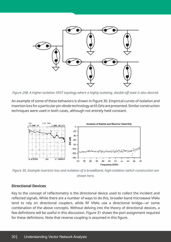
Figure 29B. A higher-isolation SPDT topology where a highly-isolating, double-off state is also desired.
An example of some of these behaviors is shown in Figure 30. Empirical curves of isolation and insertion loss for a particular pin-diode technology at 65 GHz are presented. Similar construction techniqueswereusedinbothcases,althoughnotentirelyheldconstant.
Figure 30. Example insertion loss and isolation of a broadband, high-isolation switch construction are shown here.
Directional Devices
Keytotheconceptofreflectometryisthedirectionaldeviceusedtocollecttheincidentandreflectedsignals.Whilethereareanumberofwaystodothis,broader-bandmicrowaveVNAstend to rely on directional couplers, while RF VNAs use a directional bridge—or somecombinationoftheaboveconcepts.Withoutdelvingintothetheoryofdirectionaldevices,afewdefinitionswillbeusefulinthisdiscussion.Figure31showstheportassignmentrequiredforthesedefinitions.Notethatreversecouplingisassumedinthisfigure.

31w w w . a n r i t s u . c o m
Assume the path 2 3 is the desired coupling direction.
1 2
3
Figure 31. This graphic depicts an example of a coupler block.
Coupling - S32Notethatsometimescouplingisdefinedtoincludeinsertionloss,muchlikeS31,butwithaperfectreflectionconnected.
Insertion Loss - S21
Isolation - S31
Coupling is usually dictated by the system’s signal levels; subject to the constraint thatdirectivity usually worsens (for a broadband coupler) if the coupling gets too tight. Coupling factorstherefore,usuallyendupinthe10to20dBrange,althoughthereareexceptions.Ofcourse,aminimalforwardinsertionloss(tomaximizeavailableportpower)andreasonablematch (since this may dictate raw port match and is usually connected to directivity) are desired.
The wildcard, which is principally a function of the construction techniques and level ofassemblytuning,isdirectivityorisolation.InviewofthepowerofVNAcalibrations,itisusefulto understand the importance of these raw parameters to overall system performance.
Beforeexploringthatquestion,itisnecessarytorevisittheconceptsofresidualversusrawparameters, such as directivity and source match. Raw parameters describe the physicalperformanceof the components involved (e.g., thedirectivity previously described for thedirectionaldevice).The residualdirectivity isdefinedaswhat is leftafter thecalibration. Itdescribesthequalityofthecalibrationcomponents,algorithmandtheprocess.Thisconceptis discussed in more detail in the calibration section of this section. The residuals at the time of theDUTmeasurement,describethemeasurementuncertaintyandnottherawparameters.AnindividualDUTmaybesensitivetotherawparameters(e.g.,anamplifiermayormaynotbe stable for a given raw-port match on the VNA), but themeasurement itself is largelyinvariant to them.

32 Understanding Vector Network Analysis
Figure 32. The impact of positive and negative raw directivities on a calibrated measurement is shown here. As long as the environment is stable, both calibrations are roughly equivalent.
Toseethis,considertwocalibrationsperformedonaVNA.InthefirstcalibrationtheVNAisconfigurednormallywitharawdirectivityofabout10to15dBacrossthe70kHzto70GHzfrequency band. The second calibration is performed with a 10 dB pad on the test port so that therawdirectivity(ignoringpadmismatch,sothisisanupperbound)is-5to-10dB.Witheachcalibration,thereturnlossofthesamedelaylineismeasured.TheresultsareshowninFigure32 and indicate agreement—towithin connector repeatability limits—even in the deepestnotches.Theresidualdirectivitiesaretherefore,nearlyidentical.
Good RawDirectivity Case
Raw Directivity
Actual DUTRawMeasurement
Correction
Poor RawDirectivity Case
Raw Directivity
Actual DUTRawMeasurement
Correction
Figure 33. The mathematics of directivity correction is illustrated here for two different raw directivities.

33w w w . a n r i t s u . c o m
Inapracticalsense,thisisimportantsincetherawparametershaveagreatdealofimpactonthestabilityofthecalibration.Considerthedirectivitycorrection.Inareflectionmeasurement,thedirectivityerroraddstotheDUT’sreflectedwavetoproducethenetmeasurement.Inthecorrection, thedirectivity issubtractedoutalongwithother tasksbeingperformed. If thatsubtractionissmallinmagnitude,asmalldriftintheactualamountofdirectivitywillhavelittleeffectontheendresult.Ifthesubtractionislarge,however,afairlyminordriftinthedirectivityvectorresultsinasubstantialchangeinthefinalresult(Figure33).
Itisimportanttherefore,tostriveforthebestdirectivitypossiblewithintheboundariesoftheconstraints. In theexampleofFigure32,bothmeasurementsweremadeshortlyafter thecalibrations. Had the delay line been measured several hours after the calibration, in athermally-dynamicenvironment,theresultsmighthavebeenquitedifferent.
Another constraint to consider is bandwidth. While the upper end is relatively easy to understandwiththecollapseofdirectivityunderthewavelengthlimits,thelowendisoftenmisunderstood.Obviously,as thecouplingsectionbecomeselectricallyshort, thecouplingfactor must typically fall and often does so at a 6-dB/octave rate. The available signal level decays rapidly and signal-to-noise becomes a problem. Directivity usually also suffers at this end,butmoreduetomatchproblemsthananythingelse.
Figure 34. The directivity of a RF-bridge structure is shown here. Reasonable performance down to very low frequencies is possible with the right balun structure.
Bridges are a slightly different structure and do bear some resemblance to idea of the classical WheatstoneBridge.Thedifficulty,fromaRFpoint-of-view,ishowtogeneratethenon-groundreferencednodes.Typically this isdonewitha transmission-linebalun,although thereareother alternatives. The balun helps to set the bandwidth and parasitics of the lumped components being used.
34 Understanding Vector Network Analysis
Reasonable directivity can be maintained over large frequency ranges through proper balun design. The example shown in Figure 34 can be further optimized through the use of a more elaboratebalunstructure,althoughthisoptimizationcomesattheexpenseofsomeinsertionloss.
Down Converters
Whilethereisagreatdealofcontentavailableregardingreceiverdesign,thisdiscussionwillfocusonVNA-specifictopicsanddecisions,aswellasgeneralanalyses.Withabroadband-microwaveVNA,theengineermustperformsomemeansofdownconversion.Therearemanydecisionstomake,includingthenumberofdown-conversionstagesandwithwhatfrequencyplan.
Classically,measuringreceivershaveusedmultipleupanddownconversionstoprovidebetterimagerejectionandtoallowamoreflexiblefrequencyplanforavoidingspurs.InaVNA,theimage is usually less of a concern since there is one known signal present (which may be a harmonic) that the engineer wants to measure. As the application space changes to include IMD and other more complicated measurements, image-related issues become moreprevalent,but thereare “work-arounds.”Becausesourcesarebecoming increasingly cleanandconvertersincreasinglylinear,spurproblemsareonthedecline.Couplethatwithcost,complexityandagain,withthesituationofasingle-knownsignal,andmuchofthereasoningbehind multiple conversions diminishes. Depending on how the IF is implemented and for othersignalprocessingreasons,twoconversionsaresometimesdesired,butithasbecomelesscommonthesedaystogobeyondthat.Forreasonsofstability,homodynereceivershavebeenavoidedinrecentyears,butthatmaychangeastheadaptive-conversioncircuitryusedin commercial receivers improves.
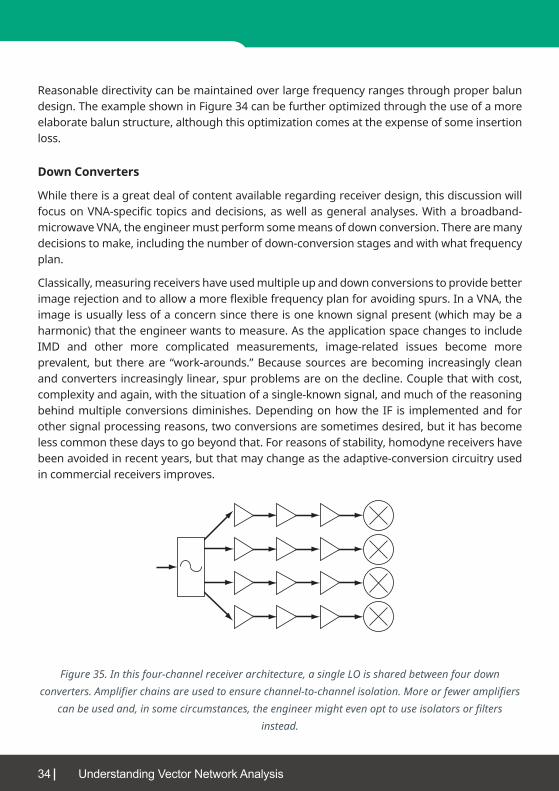
Figure 35. In this four-channel receiver architecture, a single LO is shared between four down converters. Amplifier chains are used to ensure channel-to-channel isolation. More or fewer amplifiers
can be used and, in some circumstances, the engineer might even opt to use isolators or filters instead.

35w w w . a n r i t s u . c o m
Inanidealscenario,theengineerisabletofundamentallydownconvertovertheVNA’sentirefrequencyrange.Thisallowsforthelowestspuriouspossibilities,thebestreceiver-noisefigureandprobablythebestlinearity.Inabroadband-microwavesystem,thiscangetveryexpensivesincetheisolationchainsmustrunoverthefullfrequencyrange,provideenoughLOpowerfortheconverter (10to20dBm,typical),andprovide100to120dBofround-trip isolation(Figure 35). The design engineer might opt to have a separate LO for each of the four or more converters,butthisgetsevenmoreexpensiveandmaintainingphasesynchronizationcanbechallenging (Figure 36). Some kind of harmonic-conversion process is therefore typically used to limit the required range of the LO.
Figure 36. In this four-channel receiver, each down converter has its own LO. This can be expensive at higher frequencies and challenging in terms of having to ensure adequate phase synchronization
between channels.
The common choices are mixers or samplers. Mixers are most commonly doubly balanced or double-doublebalanced,butmanyotherconfigurationsarepossible.Samplerscanbefurthersubdividedintohigh-LOandlow-LOconfigurations.Theharmonicmixerandhigh-LOsamplerhave become quite similar in many regards and their distinctions now verge on the philosophical.
36 Understanding Vector Network Analysis
OptionalBias Control
Edge Sharpener Differentiator
Edge Sharpener+ SRD
SRD
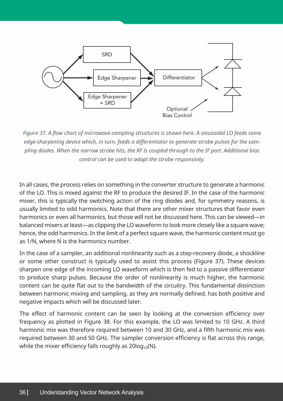
Figure 37. A flow chart of microwave-sampling structures is shown here. A sinusoidal LO feeds some edge-sharpening device which, in turn, feeds a differentiator to generate strobe pulses for the sam-pling diodes. When the narrow strobe hits, the RF is coupled through to the IF port. Additional bias
control can be used to adapt the strobe responsivity.
Inallcases,theprocessreliesonsomethingintheconverterstructuretogenerateaharmonicof the LO. This is mixed against the RF to produce the desired IF. In the case of the harmonic mixer,thisistypicallytheswitchingactionoftheringdiodesand,forsymmetryreasons,isusually limited to odd harmonics. Note that there are other mixer structures that favor even harmonicsorevenallharmonics,butthosewillnotbediscussedhere.Thiscanbeviewed—inbalancedmixersatleast—asclippingtheLOwaveformtolookmorecloselylikeasquarewave;hence,theoddharmonics.Inthelimitofaperfectsquarewave,theharmoniccontentmustgoas1/N,whereNistheharmonicsnumber.
Inthecaseofasampler,anadditionalnonlinearitysuchasastep-recoverydiode,ashocklineor some other construct is typically used to assist this process (Figure 37). These devices sharpen one edge of the incoming LO waveform which is then fed to a passive differentiator to produce sharppulses. Because theorder of nonlinearity ismuchhigher, theharmoniccontentcanbequiteflatouttothebandwidthofthecircuitry.Thisfundamentaldistinctionbetweenharmonicmixingandsampling,astheyarenormallydefined,hasbothpositiveandnegative impacts which will be discussed later.
The effect of harmonic content can be seen by looking at the conversion efficiency overfrequencyasplotted inFigure38.For thisexample, theLOwas limited to10GHz.A thirdharmonicmixwasthereforerequiredbetween10and30GHz,andafifthharmonicmixwasrequiredbetween30and50GHz.Thesamplerconversionefficiencyisflatacrossthisrange,whilethemixerefficiencyfallsroughlyas20log10(N).

37w w w . a n r i t s u . c o m
Figure 38. This graphic compares the conversion efficiency of a sampler and two example harmonic mixers. The LO is limited to 10 GHz so the harmonic mixers use harmonics 1, 3 or 5 in this picture.
Theimprovementinconversionefficiencythatresultswiththesamplerdoesnotcomefree.Sinceallof theharmonicsareconvertingwithaboutthesameefficiency, theunusedonescontribute noise to the output. If the self-conversion noise is a large part of the overall noise budget,thiscanbecomeanissue.Itisofmoreconcernwithalow-LOsamplingprocess.InFigure39,anattemptismadetonormalizeforthischangeinthenoisefloor.Insomesense,theconversionefficiencyrepresentsasignal-to-noiseratio (SNR).Theflatnessversusslopeeffectisstillvisible,buttheperformancecross-overpointmovesfromanN=1locationtoalocation that is between N=2 and N=3.

38 Understanding Vector Network Analysis
Figure 39. A normalized conversion efficiency comparison of a sampler to two example harmonic mixers is shown here. The setup is the same as in Figure 38, but the result is corrected for the different
absolute-noise output powers of the different structures.
Figure 40. The dependence of IF output power on LO power for an example fundamental mixer is shown here.
Forsamplersandtoalesserextent,harmonicmixers,whatrangeofLOtouseisanimportantquestion. A lower LO means higher numbers of multiples will be in play which increases the noise delivered to the IF. It also increases the likelihood of spurious responses coinciding with thesourceand/orDUTspursandharmonics;resultinginamorechallengingfrequencyplan.A higher LO requires more expensive LO hardware and the system is less able to provide additional information about the incoming signal. The latter is an attribute not normally associatedwiththeVNA,althoughithasbeenusedinlarge-signalimplementationstocaptureand analyze the harmonics and/or modulation components of the DUT’s output signal.

39w w w . a n r i t s u . c o m
Figure 41. The dependence of IF output power on LO power for an example sampler is shown here. The result saturates for an ordinary fundamental mixer.
Another important topic is LO-power dependence. As LO power increases, the mixer’sperformance saturates and its behavior becomes less sensitive to minor variations in LO power (Figure 40). Depending on the drive configuration, the same tends to be true in asampler(Figure41).Onceasufficientlylargegatingpulseisgenerated,furtherincreasesdolittle to the gating aperture. It is important to note, however, that there can be somefundamental amplitude modulation/phase modulation (AM/PM) in this process since the sharpest point of the pulse moves in time as the amplitude changes.
There is more LO-power dependence in a harmonic-mix process since true square-wave generation is only approached in a loosely asymptotic manner (Figure 42). The drive levels havetobequitehightoreachasaturationlevel.Insomecases,itmayevenvergeonadamagelevel,dependingonthestructureandthetechnology.ThesametypeofAM/PMconversioncan occur here with the samplers since the edge shape is still somewhat critical to the harmonic phasing.
Linearity is a critical topic in any discussion of the VNA receiver and is normally the firstconverterthatestablishesthelimit.Forfundamentalmixing,manyrules-of-thumbexistforthe third-order intercept (TOI) for various mixer topologies. A common value for doubly-balanced mixers is that the input-referred TOI point (IP3) is roughly equal to the LO power. In theexamplespreviously cited, theanalysesare somewhatmore complicatedby themorehighly,non-linearmixingprocessesinvolved.Ingeneralthough,theIP3willdegrade.

40 Understanding Vector Network Analysis
Figure 42. The dependence of IF output power on LO power for two levels of harmonic mix is shown here. Due to the required harmonic generation in the mixer and the soft conversion curve of this par-
ticular device, saturation is more difficult to achieve.
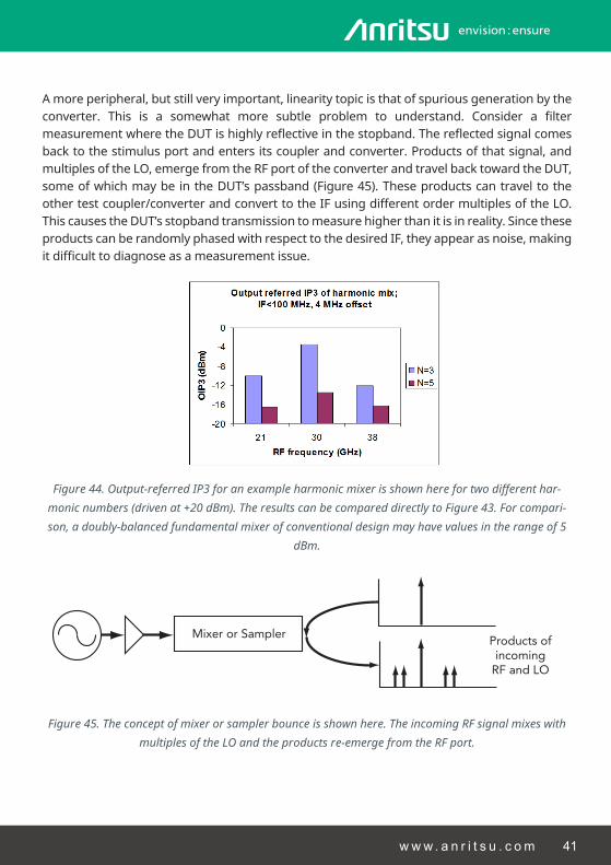
The plot of a shockline sampler being driven with 20 dBm is shown in Figure 43. It depicts a veryflatinterceptwithfrequency.Theharmonicmixerresults(doubly-balancedmixersdrivenwith 17 dBm) show a quickly degrading IP3 with harmonic number (Figure 44). This might be expected since the available LO power is degrading and is limited by the mixing diodes’ series resistance.Compression,anothercommonlyquotedmeasureoflinearity,typicallytrackstheintercept point in a relative sense.
Figure 43. Example output-referred IP3 of a sampler is shown here. Since the conversion loss is on the order of 10 to 12 dB, the input-referred values are on the order of
15 to 20 dB.
41w w w . a n r i t s u . c o m
Amoreperipheral,butstillveryimportant,linearitytopicisthatofspuriousgenerationbytheconverter. This is a somewhat more subtle problem to understand. Consider a filtermeasurementwheretheDUTishighlyreflectiveinthestopband.Thereflectedsignalcomesbacktothestimulusportandentersitscouplerandconverter.Productsofthatsignal,andmultiplesoftheLO,emergefromtheRFportoftheconverterandtravelbacktowardtheDUT,some of which may be in the DUT’s passband (Figure 45). These products can travel to the other test coupler/converter and convert to the IF using different order multiples of the LO. This causes the DUT’s stopband transmission to measure higher than it is in reality. Since these productscanberandomlyphasedwithrespecttothedesiredIF,theyappearasnoise,makingitdifficulttodiagnoseasameasurementissue.
Figure 44. Output-referred IP3 for an example harmonic mixer is shown here for two different har-monic numbers (driven at +20 dBm). The results can be compared directly to Figure 43. For compari-son, a doubly-balanced fundamental mixer of conventional design may have values in the range of 5
dBm.
Products of incoming
RF and LO
Mixer or Sampler
Figure 45. The concept of mixer or sampler bounce is shown here. The incoming RF signal mixes with multiples of the LO and the products re-emerge from the RF port.

42 Understanding Vector Network Analysis
AsshowninFigure46,bothsamplersandharmonicmixerscanbesusceptibletothisissue,although the relative frequencies of the problem products are usually different. Typically when aharmonicmixerisoperatingatN>1,thelowerorder-relatedproductsaremoreproblematicbecausetheconversionefficienciesarefavorable. Inthecaseofasampler, theconversionefficienciesareequallyweighted(uptoapoint),soitisoftenthoseproductsrelatedtothehigherordersthatcreateaproblem.IntheexperimentofFigure46,theLOandRFdrivelevelswere fixed, as was the IF frequency. At each test frequency, the worst-case regeneratedproductwasmeasured,inabsolutepowerterms,andtheresultplotted.
Figure 46. A comparison of bounce products for a harmonic mixer (N=3) and a sampler (N=2 to 3) is shown here. In both cases, LO drive is +20 dBm.
Thereareanumberofwaystoamelioratethisproblem,suchasbyincludingpaddingineachsamplerpath,usingisolationamplifiersonthesampler/mixerRFportsandturningoffatestsampler/mixer (with bias or LO power) when not in use. Each of these options has its drawbacks:
• A pad reduces dynamic range.• ARFpre-amplifiermaycausecompressionissuesormayhavestabilityissues,sincetheamplifiersinthevariouschannelsarenotidentical.
• Turning off unused converters can increase overall measurement time.
43w w w . a n r i t s u . c o m
IF Section
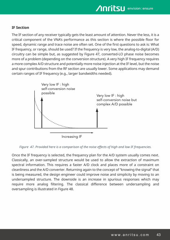
TheIFsectionofanyreceivertypicallygetstheleastamountofattention.Nevertheless,itisacriticalcomponentof theVNA’sperformanceasthissection iswherethepossiblefloorforspeed,dynamicrangeandtracenoiseareoftenset.Oneofthefirstquestionstoaskis:WhatIFfrequency,orrange,shouldbeused?Ifthefrequencyisverylow,theanalog-to-digital(A/D)circuitrycanbesimplebut,assuggestedbyFigure47,converted-LOphasenoisebecomesmore of a problem (depending on the conversion structure). A very high IF frequency requires amorecomplexA/DstructureandpotentiallymorenoiseinjectionattheIFlevel,butthenoiseand spur contributions from the RF section are usually lower. Some applications may demand certainrangesofIFfrequency(e.g.,largerbandwidthsneeded).
Increasing IF
Very low IF : high self-conversion noise possible
Very low IF : high self-conversion noise but complex A/D possible
Figure 47. Provided here is a comparison of the noise effects of high and low IF frequencies.
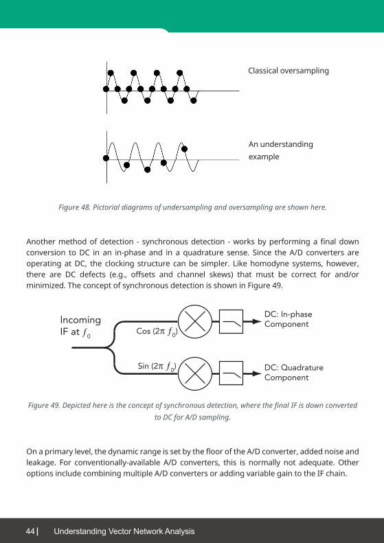
OncetheIFfrequencyisselected,thefrequencyplanfortheA/Dsystemusuallycomesnext.Classically, an over-sampled structurewould be used to allow the extraction ofmaximumspectral information. This requires a faster A/D clock and places more of a constraint on cleanlinessandtheA/Dconverter.Returningagaintotheconceptof“knowingthesignal”thatisbeingmeasured,thedesignengineercouldimprovenoiseandsimplicitybymovingtoanundersampled structure. The downside is an increase in spurious responses which may require more analog filtering. The classical difference between undersampling andoversampling is illustrated in Figure 48.
44 Understanding Vector Network Analysis
Figure 48. Pictorial diagrams of undersampling and oversampling are shown here.
Anothermethodofdetection - synchronousdetection -worksbyperformingafinaldownconversion to DC in an in-phase and in a quadrature sense. Since the A/D converters are operatingatDC, the clocking structure canbe simpler. Likehomodyne systems,however,there are DC defects (e.g., offsets and channel skews) that must be correct for and/orminimized. The concept of synchronous detection is shown in Figure 49.
Cos (2 ƒ0)
DC: In-phaseComponent
DC: QuadratureComponent
IncomingIF at ƒ0
Sin (2 ƒ0)
Figure 49. Depicted here is the concept of synchronous detection, where the final IF is down converted to DC for A/D sampling.
Onaprimarylevel,thedynamicrangeissetbytheflooroftheA/Dconverter,addednoiseandleakage. For conventionally-available A/D converters, this is normally not adequate.Otheroptions include combining multiple A/D converters or adding variable gain to the IF chain.
Classical oversampling
An understandingexample

45w w w . a n r i t s u . c o m
The former is easier to implement froma statemachinepoint-of-view,but calibrating thetransition between converters can be challenging. The latter is relatively simple from a calibrationpoint-of-view,butthemeasurementenginemustbeabletomakedecisionson-the-flyregardinghowmuchgaintoadd.Itmustthenalsobeabletoforcere-measurements,ifnecessary. Both schemes are shown in Figure 50.
ADC2
ADC2
ADC1
(A)
(B)
Figure 50. Two different methods of increasing the effective dynamic range of a digitizer are shown here. (A) illustrates the use of multiple A/D converters with a signal level offset, while (B) illustrates the
use of variable gain prior to the A/D converter.
Implementationoffilteringisanothermajortopic.Usuallysomeanalogfilteringisrequiredtohandle aliases, images and other known large interferers, to avoid overloading any IFamplifiers or A/D converters. Filtering is also required for noise reduction and sometimesreductionofcloseinterferers.InVNAs,thisisknownasanIFbandwidth(IFBW),althoughananalogousconceptofresolutionbandwidthappliestospectrumanalysis.Historically, IFBWwasdonewithacollectionofanalogfilters,butissuesofstabilityandmeasurementaccuracyarose when changing the setting between calibration and measurement. More recent instrumentsimplementthisfilteringdigitally.AcommonfilteringimplementationisshowninFigure 51.
Figure 51. In this common IF-filtering scheme, some simple filtering is analog but most of the variable filtering (and narrow-bandwidth filtering) is done digitally.
IF formreceivers
Simple filtering for aliases,
images known spurs
ADC
DSP: Digital filtering for noise control; deimination and other processing

46 Understanding Vector Network Analysis
System Performance Considerations
While interpretation of VNA specifications has been presented elsewhere, it is useful toexamine how the performance of the blocks discussed thus far will impact those performance parameters.
1. Dynamic Range-Therearetwopartstodynamicrange:noisefloorandmaximumpower.Thelatterisaddressedeitherbycompressionorportpower.Noiseflooris impacted by front-end loss (e.g., couplers and attenuators), mixer/samplerconversionlossandinitialIFgainstages.ARFpre-amplifiercanhelp at the potential expense of compression and stability.
2. Trace Noise-Usuallytracenoiseismeasuredfarawayfromthenoisefloortoavoidanyimpact. LO/source-phase noise folds over and converts to the IF. Trace noise also impacts IF system noise.
3. Port Power - Port power comes from the source power and the loss between source and port. Compression limits of switches and other test-set components may play a role.
4. Power Accuracy-Generally, power accuracy is limitedby the structureof theALC loop,temperaturecompensationemployed,calibrationprocedure,andpowerranges involved.
5. Harmonics - Usually harmonics come from the source and related components.
6. Compression-Usuallythemixer/samplerlinearitysetsthecompressionlimit,althoughtheIF can sometimes contribute. While RF attenuators can help in some applications,front-endRFamplifierscanmakethecompressionlimitworse.
7. Raw Port Parameters-Thefront-endcomponents(e.g.,couplers,attenuatorsandtransferswitches) tend to set these parameters.
8. Residual Port Parameters-Generally, the calibration kit and calibration algorithms setthese limits. The first instrument parameters to affect theresiduals are usually linearity-related.
9. Stability-Manyfactors,someofwhicharehardtomeasure(e.g.,measurementdynamics),affect stability. For example, temperature stability of couplers, switches andcablesaffectsthesystem,asdoesLO-powerstabilityandthesensitivityofthemixer/sampler to its changes. The linearity of the system and stability of port power are two other factors affecting stability.
AlloftheblocksdiscussedplayaroleinhowtheVNAperformsandhowthesespecificationsare created.
47w w w . a n r i t s u . c o m
Measurement Fundamentals
The VNA represents a large suite of measurement capabilities. What follows are a few central concepts and vocabulary which will prove useful in any VNA discussion.
The Reference Plane
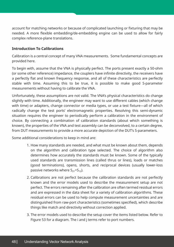
Perhapsoneofthemostimportant,andyetpoorlyunderstood,S-parametermeasurementconcepts is the reference plane. When performing a RF calibration with short-open-load-thru (SOLT),line-reflect-line(LRL)orsomeotheralgorithm,theengineerimplicitlyestablishesasetof planes (one per port) that serve as the reference for the calibration. Imagine that two of theseplanesdescribeapairoflocationswhere,ifaperfectthrucouldbeconnectedbetweenthem,S21 and S12 would be precisely unity (0 phase) and S11 and S22 would be precisely 0 - excluding residual calibration errors. This can become an issue when things like adapters and fixturesareaddedorchangedbetweencalibrationandmeasurement.Themeasuredphasesand amplitudes will be incorrect due to the distortions caused by those additions/changes. Whiletheeffectsmaybeinsignificantatlowfrequencies,theycanbequitelargeabove30or40 GHz.
ThisconceptisshowninFigure52.Supposethecalibrationisperformedatplanes1Aand2A,while the DUT is connected to planes 1B and 2B (the horizontal lines between those planes maybeadaptersorfixtureparts).BothreflectionandtransmissionphasesarealteredbytheelectricallengthbetweentheAandBplanesoftherelevantport(s).Reflectionandtransmissionmagnitudes are altered by any loss (or change of loss) between these planes.
VNA
1A 1B 2B 2A
Figure 52. According to the reference plane concept, if adapters, fixtures and cables are added/changed after a calibration, distortions can result.
If the characteristic impedances of any elements in this figure change, or if the desiredreference impedance changes, the situation becomes more complicated. Since any line/reference-impedance deviation makes the length change act like a transformer, largedistortions are possible.
Insomecases,itmaybedesirabletoallowtheseplanedistinctionstobemorecomplex—to
48 Understanding Vector Network Analysis
accountformatchingnetworksorbecauseofcomplicatedlaunchingorfixturingthatmaybeneeded. Amore flexible embedding/de-embedding engine can be used to allow for fairlycomplex reference-plane translations.
Introduction To Calibrations
Calibration is a central concept of many VNA measurements. Some fundamental concepts are provided here.
Tobeginwith,assumethattheVNAisphysicallyperfect.Theportspresentexactlya50-ohm(orsomeotherreference)impedance,thecouplershaveinfinitedirectivity,thereceivershaveaperfectlyflatandknownfrequencyresponse,andallofthesecharacteristicsareperfectlystable with time. Assuming this to be true, it is possible to make good S-parametermeasurements without having to calibrate the VNA.
Unfortunately,theseassumptionsarenotvalid.TheVNA’sphysicalcharacteristicsdochangeslightlywithtime.Additionally,theengineermaywanttousedifferentcables(whichchangewithtime)oradapters,changeconnectorormediatypes,oruseatestfixture—allofwhichradically change the test ports’ electromagnetic properties. Resolving this semi-dynamic situation requires the engineer to periodically perform a calibration in the environment of choice. By connecting a combination of calibration standards (about which something is known),thepropertiesoftheVNAandtestassemblycanbedeconvolved,toacertaindegree,from DUT measurements to provide a more accurate depiction of the DUT’s S-parameters.
Some additional considerations to keep in mind are:
1.Howmanystandardsareneeded,andwhatmustbeknownaboutthem,dependson the algorithm and calibration type selected. The choice of algorithm also determines how accurately the standards must be known. Some of the typically used standards are transmission lines (called thrus or lines), loads ormatches(good terminations), opens, shorts, and reciprocal devices (usually lower-losspassive networks where S21=S12).
2. Calibrations are not perfect because the calibration standards are not perfectly known and the error models used to describe the measurement setup are not perfect. The errors remaining after the calibration are often termed residual errors and are expressed in the data sheet for a variety of calibration algorithms. These residual errors can be used to help compute measurement uncertainties and are distinguishedfromraw-portcharacteristics(sometimesspecified),whichdescribethings like match and directivity without correction applied.
3. The error models used to describe the setup cover the items listed below. Refer to Figure 53 for a diagram. The i and j terms refer to port numbers.

49w w w . a n r i t s u . c o m
• Source Match (epiS) - Corrects for the imperfect match of a measurement reference plane when that port is driving.
• Load Match (epiL) -Sameasabove,butwhentheportactsasatermination.Somealgorithmsdo not use this term. Instead they use a pre-correction step to account for any differences between source match and load match.
• Directivity (edi) -Correctsforimperfectionsinthecouplers,whichleadtoameasuredreflectionevenwhenaperfectterminationisattached.
• Reflection Tracking (etii)-Frequencyresponseofthesystemwhenmeasuringareflection.• Transmission Tracking (etij) -Sameasabove,exceptwhenmakingatransmissionmeasurement.Thistermisnotentirelyindependentofreflectiontracking.Somealgorithmsuse this information.
• Isolation (exij) - Corrects for some leakages between the system’s receivers and source. While mostalgorithmssupportsomeaspectofisolation,itisnotcommonlyusedduetorelativelysmall improvements.
ex21 and ex12Perfect VNA Port Perfect VNA Port
DUT
A
B
C
D
ed1 ep1S ep2S ed2
et11 = A * Bet22 = C * Det21 = A * Det12 = C * B
Figure 53. In this diagram of the error model, the idea is to replace the physical VNA ports with ideal VNA ports connected to simple networks containing all of the imperfections (called error boxes).
4. Sometimes it is not convenient to calibrate all the way up to the reference planes attheDUT.Insuchcases,techniquessuchasde-embeddingandreference-planeextensionareused tohelp correct foranydiscrepancies. In somesense, thesetechniquesare like calibration (andmayusemuchof thesamemath),but relymoreonmodels(circuit-basedorfile-baseddescriptionsofthenetworksinvolved)rather than measurements of standards through the networks in question. Some combination of these approaches may be appropriate depending on the measurement setup involved.
50 Understanding Vector Network Analysis
5.Calibrationsdonotlastforever.Astemperaturechanges,cablebehaviorschange.Withmanycable-bendingcycles,thephaseshiftthroughthosecablesmaychange.Replacements of cables or adapters change the calibration. Calibrations can last anywherefromafewhourstoafewdays,butitdependsgreatlyontheenvironmentand the desired stability.
Linearity
AfundamentalassumptioninmostVNAmeasurementsisthatthesystemislinear.Commonly,thisisexpressedeitherintermsofcompressionorTOI,asfollows:
Compression example: 0.1 dB compression occurs at a port power of 10 dBm.
TOI example: Givenatonespacingof1MHzandaportpowerof-10dBm,theTOIis35dBm.
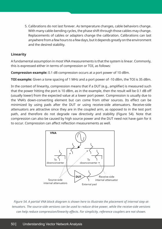
Inthecontextoflinearity,compressionmeansthatifaDUT(e.g.,amplifier)ismeasuredsuchthatthepowerhittingtheportis10dBm,asintheexample,thentheresultwillbe0.1dBoff(usually lower) from the expected value at a lower port power. Compression is usually due to the VNA’s down-converting element but can come from other sources. Its effect can be minimized by using pads after the DUT or using receive-side attenuators. Receive-side attenuatorsareattractivesincetheyareinthecoupledarm,asopposedtointhetestportpath, and therefore do not degrade raw directivity and stability (Figure 54). Note thatcompression can also be caused by high source power and the DUT need not have gain for it tooccur.Compressioncanaffectreflectionmeasurementsaswell.
Figure 54. A partial VNA block diagram is shown here to illustrate the placement of internal step at-tenuators. The source-side versions can be used to reduce drive power, while the receive-side versions
can help reduce compression/linearity effects. For simplicity, reference couplers are not shown.
Todownconverter
Todownconverter
VNA
DUT Receive-sideinternal attenuatorSource-side
internal attenuators External pad

51w w w . a n r i t s u . c o m
TOI is an analogous way of expressing the receiver’s linearity, although the quantity issomewhat different. This specification is important when using the VNA to measureintermodulation products or a DUT’s TOIs.
While less common, linearity can sometimes be an issue at lower-signal levels. Here, thenonlinearitiesofA/Dconverterstendtoappear.Usuallythough,enoughgainisusedintheVNA to prevent this from becoming an issue. Other IF and RF chain nonlinearities can be present aswell, but areusuallynot explicitly specified. Theyare typically accounted for inuncertainty calculations.
Data Formats
AlargenumberoffileformatsanddataformatsareusedbytheVNA.Thetwomainclassespertaining to users are DATA and Text. The DATA class contains a number of export formats whichareavailableforuseinexternalapplicationsorforarchiving.Incontrast,theText(.txtextension)classisatab-delimitedformat,withanoptionaldescriptiveheader,inwhicheverytrace’s data in the active channel is saved to a desired location. Each trace’s data is saved as an XandYcolumn(e.g.,toaccommodatemixedfrequencyandtimedomain).Subsequenttracesare added as additional columns.
Some of the common formats include:
• Common-Separated(.csv)—Amorespreadsheet-friendlyversionoftheTextclass.• Bitmaps(.bmp)—Agraphicscaptureofthedataandmenuareas.• .snp(.s1p,.s2p)—Thestandardmicrowavesimulatortext-dataformat.Thisissimilarto.txtexceptacontrolledheaderisusedandonlyoneorfourS-parametersaresaved.Ifa.s2pfileisrequested,butallS-parametersarenotbeingmeasured,a“0”isenteredforthemissingS-parameters.Ifafull2-portcalibrationisapplied,allS-parametersaremeasuredbutneednotbedisplayed.Inthiscasethe.s2pfileiscomplete.Notethat,unlikethepreviousfiletypes,.snpfilescanberecalledanddisplayedastracememory.Theyareloadedintotheactivechannel.
• TraceMemoryFormatted(.tdf)—Thissavestheactivetrace’smemoryfollowingpostprocessingand is useful for comparing against a ‘golden device’ to see if a DUT’s performance has changed.
• TraceMemoryUnformatted(.tdu)—Sameasabove,butoccursbeforemosttracepost-processing(e.g.,timedomain,smoothingandgroup-delaycalculations).
Note that these last two formats can be recalled into the active trace, but the VNAmustnormally be in hold or sweeping very slowly for this to be useful. They can also be recalled into the active trace’s memory. The trace can later be recalled into the same part of the chain where it was saved. Formatted trace memory is recalled after post-processing steps, whileunformatted trace memory is recalled before those steps.

52 Understanding Vector Network Analysis
Other Terms of Interest
Afewothercommontermsofinterestaredefinedbelow.Moredetailcanbefoundthroughoutthis book.
Power - Power delivered to the port when that port is driving.
Scale -ThedB/divorunits/divofagivengraph.ItalsodefinesthemagnificationoftheSmithchart graph.
Limit Lines - Test values on a graph that can be used to mark a DUT as pass or fail. Upper and lowervaluescanbedefinedforapoint,orarangeofpoints,thatmayindicatespecificationsfor the DUT.
Interpolation - A means of acquiring information between calibration or measurement points. This term is used in a number of contexts within the VNA.
• Calibrations - Normally measurements can only be made at frequency points where a calibrationwasperformed.Byenablinginterpolation,thesystemattemptstocalculateerrorcoefficientsatotherpointsinbetween.Someerrormayresult,butitcanbeveryconvenient.
• Embedding/De-Embedding -Whenafileisloadedthatdescribesanetworktobeembedded/de-embedded,itsfrequencylistmaynotexactlymatchthefrequenciesbeingswept.Inthiscase,thesystemwillattempttointerpolatethedatatothefrequenciesbeingused.
• Markers - Normally,indiscretemode,twomarkershopbetweenfrequencypointsbeingmeasured.Incontinuousmode,themarkersgotootherfrequenciesanddisplaydatavaluesbased on interpolation between measurement points.
System Architecture And Modes Of Operation - The VNA’s flexibility provides uniqueopportunities for specialized configuration. It is helpful to understand the differences insystem architecture that can be found in different VNAs. Understanding the strengths and limitations of different VNA system architecture helps in choosing the best VNA for a particular applicationandinconfiguringthemeasurementforoptimumresults.Thedifferentmodesofoperation and types of system architecture include:
• Receiver Offset Mode - This mode allows for independent source and receive functions for mixer,harmonics,IMD,andothermeasurementswherethesourceandreceivefrequenciesare offset.
• Source Modes - Some non-Anritsu VNAs provide synthesized (step) mode and non-synthesized (open-loop)modesofoperation.VerifythattheVNAisproperlyconfiguredforsynthesizedmode to ensure accurate phase measurements. Verify also that the VNA has the best trace noise to ensure accurate transmission tracking.
• IF Chain Methodology - Microwave VNAs convert the RF signal to IF before analysis. There are differentmethodsofdownconversion,buttheyusuallyfallintotwocategories:harmonicsampling and harmonic mixing. VNAs utilizing harmonic mixing often have a lower

53w w w . a n r i t s u . c o m
compression point so care must be taken to ensure that accuracy is not lost due to compression errors.
• Receiver Calibration - UnlikeconventionalVNARFcalibrations(e.g.,SOLTandLRL/LRM)thatareusedtocalibratetheVNAforS-parametermeasurements,thereceivercalibrationismoreof an absolute power calibration to help with measurements like:
• Harmonics• IMD,IP3andothermulti-tonedistortionmeasurements• Mixer-conversionloss,insimplerscalarcases• Other times when the VNA is used just as a channelized receiver
Theideabehindreceivercalibrationistotakeaknownsourcepower,atsomesource-referenceplane,andtransferthatknowledgetothereceiveratadesiredreceiver-referenceplane.Ifitisconvenienttousethetestportasthesource-referenceplace,thebuilt-infactoryALCcalibrationcanbeusedtoestablishthe‘powerknowledge.’Ifthisisnotconvenient—becauseoffrequencytranslationortherequirementforsomeothernetworkorgreateraccuracy—thenapowercalibration can be performed with the help of a GPIB-controlled power meter to establish that power knowledge.
Specifications and Measurement Accuracy
Specificationshelptheuserdeterminethelevelofmeasurementaccuracyavailablefromaninstrumentunderagivensetofconditions.WhenconsideringtheVNA,specificationssuchasdynamicrange,noisefloorandavailablepowerprovideinformationontheDUTconditionsthatcanbemeasuredandarenotintrinsically“accuracyspecifications.”
Measurementaccuracyisdeterminedbyfactorssuchasdirectivity,sourceandloadmatch,and isolation. These factors are often presented in the form of raw uncorrected performance and/orresidualperformanceaftercalibration.Inaddition,theS-parameterperformanceofthe DUT also contributes to the overall measurement accuracy as it interacts with the residual performanceoftheVNA.Whenconsideringmeasurementaccuracy,itisimportanttotakeintoaccountallparametersof theVNA’sresidualperformance,combinedwiththeS-parameterperformance of the DUT at each frequency point-of-interest.
Figure 55 provides an example of the transmission uncertainty for different S21 DUT characteristics over the frequency span from 20 to 70 GHz. The plot provides an indication of the complexity of calculating measurement accuracy for each device of interest. In order to helpgenerateuncertaintycurvesforindividualdevices,asoftwaretoolwasdevelopedandisavailable on the Anritsu website (www.anritsu.com). This program takes into account all salient performanceparametersoftheVNAandplotsuncertaintycurvesforspecificlevelsofDUTperformance.

54 Understanding Vector Network Analysis
Figure 55. An uncertainty plot provides the overall measurement uncertainty, taking into account all system residuals and DUT performance.
What follows is a summary of some of the important characteristics that determine the VNA’s
measurement-performance level. In some cases a brief description is provided on how to
measure the corrected residual performance.
1. Dynamic Range - This isacalculatedvaluebasedonnoisefloorandeitherthecompression level (for receiver dynamic range) or maximum port power (for system dynamic range). For dynamic-range values referenced to a direct-receiver accessport,thecompressionlevelisreferredtothatinput.Forsystemdynamicrange,themaximumavailableport-powerlevelfromthetestset—wellwithinthe0.1dBcompressionlevel—isused.
2. Compression Level - This is the receiver power level at which the reported value is 0.1 dB below what is expected based on lower power results. Due to the accuracy required, this almost always is computed as a ratioed measurement where asecond receiver gets a padded version of the signal fed to the target receiver. The second receiver is well away from compression and therefore, no inadvertentcancellation of distortion occurs. Padding is typically used to minimize match interactions. In general, compression is referred to test ports but can also bereferred to direct receiver-access ports. A diagram is shown in Figure 56. For the directreceiver-accessports,thesetupisrelativelyeasytoimplement.Forthemain
Magnitude Measurement Uncertainty

55w w w . a n r i t s u . c o m
test-port-based test receivers, a thru line and the internal source are used toprovide drive. The driving-port test receiver is used as the norming receiver. Since thisreceiverseesaload-matchvalue,ithasthedesiredeffectofreducingitsdrivelevel well below compression.
To Norming Receiver
To TargetReceiver
Figure 56. A schematic diagram of a compression-test setup is shown here.
Aspreviouslydiscussed, a ratioedmeasurement isnormally required. In the two test-portcase,thisratioisnormally|b2/b1|or|b1/b2|.Thisparameterissweptatlowpower(-15dBm)inamodestIFBW(e.g.,100Hz)sothattracenoiseismuchsmallerthanthedesiredcompressionlevel to be observed. This data is stored to memory and used for normalization. The drive power is then increased until the indicated level of compression occurs (typically 0.1 dB). The drive power at the subject port when this occurs forms the result of the measurement. Althoughthetermcompressionisused,expansionmaysometimesbeobservedduetomatchinteraction. Deviation in either direction is counted in this measurement.
3. Noise Floor -Thisisameasureinabsolutepower(dBm)ofthenoisefloorofthesystem referenced to the test port. Typically this is calculated by measuring S21 and S12 with a short-thru line connected and the port power set to some value X. The cablelossisnormallysubtractedseparatelyor,alternatively,aflat-powercalibrationcan be performed at the end of the cable. The traces are normalized with this thru in place. The ports are then terminated with loads (typically), and S21 and S12
measured in a 10 Hz bandwidth with no averaging. A minimum of 10 sweeps are acquired in linear magnitude mode and the root-mean-square (RMS) value is computed at each frequency point individually. This result is then normally converted back to log magnitude.
4. Trace Noise (High Level Noise) - This is a measure of the scatter of data when measuring a high-level signal (full reflect or transmission through a shorttransmission line).Themeasurement isspecifiedatdefaultpowerwitha1kHzIFBW and default auto-reduction for frequencies below 3 MHz. The measurement

56 Understanding Vector Network Analysis
is performed by acquiring a minimum of 10 sweeps of data from the desired parameter, in linearmagnitudeandphase,afteratrace-mathnormalization.Ateachfrequencypoint,thepopulation-basedstandarddeviationiscomputed.ThisformstheRMShigh-levelnoisenumber.Formagnitude,thisisnormallyconvertedback to log magnitude.
5. Power Range - Maximum port power is determined by the power at which the system is still leveled. The same applies to minimum power when step attenuators are not involved. For those systems with attenuator options, the maximumattenuator value for the model is subtracted from the minimum ALC power to get the minimum system power.
6. ALC Power Accuracy And Linearity - Power accuracy and linearity are both determined with an external power meter. Accuracy is evaluated at default power across frequency. Linearity is evaluated over both power and frequency with the reference being the value at default.
7. Frequency Accuracy And Stability - Frequency stability is a pass-through specificationofthe10MHztimebaseandisnottestedseparatelyatinstrumentlevel. Accuracy is measured using a frequency counter synchronized to a GPS-based time base after the 10 MHz calibration is complete.
8. Harmonics - This is also port-referred and based on default power. It can be calculatedas follows,usingaproperly-calibratedspectrumanalyzeror theVNAitself,usingmultiplesourcecontrol:
• Choose b2/1 as the measurement variable.• Performaflat-powercalibrationattheendofacablefromport1overtheentirerangeofthe
instrument.• Perform a receiver calibration on b2.• Withmultiplesourceequationsallsetto1/1(f+0),acquiredataandnormalize.• Changethereceiverandreceiversourceequationtolookforthedesiredharmonic(e.g.,
2/1(f+0) for the 2nd harmonic).
9. Raw Directivity - This expresses the raw directivity of the test coupler assemblies as affected by internal match conditions. While it could be measured directly using direct-access loop options, it is normally done through the calibration engine.Perform a reasonably high-quality calibration and compute the term edx/etxx,where ‘x’ refers to the port in question. The magnitude of this term represents the rawdirectivity.Usetheform-20log10|edx/etxx|togetthevalueintheformofaspecification.
10. Raw Source Match - Much like rawdirectivity, this canbeextracted fromthe

57w w w . a n r i t s u . c o m
calibrationsystem.Theappropriatevalueis-20log10|epxS|,where‘x’istheportin question.
11. Raw Load Match - This can also be extracted from the calibration system. Perform the calibration so that the reference plane is at the test port of the port under study.Thevalue inthiscase is -20log10|epxL|.Alternatively,performa1-portcalibration at the end of a cable and then connect this cable to the port under study. The direct measurement in this case yields raw load match.
12. Residual Directivity -Residualsareallbasedonafter-calibrationresultsand,assuch, reflect imperfections in the calibration. The residuals are determinedprimarily by the calibration method/algorithm, the calibration componentsinvolvedandtheskillofthepersonperformingthecalibrationandverification.The residual measurements are generally traceable to airline standards which form the impedance reference for VNA measurements. Directivity is measured using an airline attached to the test port and terminated in either a load (preferred for broadband) or an offset (acceptable for lower frequencies). A ripple extraction method is applied to the resulting Sii data to determine the directivity. In an automated setup, circle-fitting and polynomial-fitting routines are commonlyused,buteachhas itsweaknesses.Anadaptivesortingalgorithm isgenerallyadvised.
13. Residual Source Match - This is also an airline ripple measurement but is performed with the airline shorted.
14. Residual Load Match - This isadirect reflectionmeasurementwitha thruorairline connected after calibration.
15. Residual Reflection Tracking - Thisisadirect-reflectionmeasurementofashort,but not the one used during calibration for the case of a defined standardscalibrationsuchasSOLT, short-short-load-thru (SSLT)or short-short-short-thru(SSST).Thepeakdeviationfromalinearfitisusedasthestartingpointtoremovethe effect of loss of the short standard. The contribution due to source match and tracenoiseisthenremovedfromthatresulttogetreflectiontracking.
16. Residual Transmission Tracking - This is a direct-transmission measurement of athruorairline,dependingonthecalibration.Thepeakdeviationfromalinearfitis again used as the starting point. The contribution due to the load-match source match interaction and that due to trace noise is removed from the result to get transmission tracking.

58 Understanding Vector Network Analysis
Vector Network Analyzers - VectorStar
AnritsuVNAsencompassawiderangeofhighperformancesolutionsforR&D,manufacturing,and field applications in the wireless, satellite, defense, broadband communication, andoptoelectronic components markets. Choose between the VectorStar, Shockline or VNAMasterfamilyfortheperfectsolutionofadvancedperformance,accuracy,andreliability.Idealfor measuring any RF and Microwave component or system - from design and manufacturing tomeasurementsanytime,anywhere.
MS4640B Series VectorStar Vector Network Analyzer• Broadestfrequencyrangefrom70kHzto145GHzsinglesweep,andupto1.1THzin
waveguide bands.• Superior dynamic range - up to 140 dB.
The world’s widest frequency range in a single instrument – 70 kHz up to 70 GHz. Massive 106 dBdynamicrangeat70GHz.Sweepfrom70kHzto70GHz in less than4ms, lockedandlevelled.AndinnovativePrecisionAutoCalcalibrationmakestestroutineconfigurationeasy. Whether you are testing performance characteristics of on-wafer devices or developing communicationssystemsforaerospace,militaryorsecurityuse,theMS4640Bisthebestthatmoney can buy.

59w w w . a n r i t s u . c o m
Vector Network Analyzers - ShockLineTM
• Patented ShockLineTM VNA-on-a-chip technology.• A radical departure from conventional VNA design.• Highaccuracy,sensitivityandsweepspeeds.• ConsiderablymorecostefficientthancomparablebenchtopVNAs.
Features Benets Applications
• Obtain the most thorough and accurate broadband device characterization • Eliminate time consuming concatenation process across the RF, microwave/mm-wave bands• Decrease test instrument expenses by eliminating the need for a 2nd RF VNA• Reduce the risk of DC extrapolation errors in your device modelling
• Increase manufacturing revenue by increasing throughput.
• Quickly and easily spot the most hard to find failures and reduce the risk of shipping defective products
Broadest frequency spanfrom a single coaxial test port covering 70* kHz to 70 GHz in a single instrument and 70 kHz to 110/125/145 GHz in the broadband configuration. * When Option 070 70 kHz is included
Fast swept synthesized measurement speed <30 usec per point
• Accurately measure medium and high loss devices
• Catch all potential feedthroughs in out-of-band regionsSuperior Dynamic Range - up to 140 dB
High compression point -up to 15 dBm at 70 GHz
• Eliminate the need for additional attenuators • Improve calibration and measurement accuracy
Best test port characteristic -up to 50 dB Directivity, Source Match, Load Match.
• Reduce measurement uncertainty • Reduce measurement guard bands• Improve productivity• Optimum precision in R&D
Highest point resolution - 100,000 points
• Zoom in on narrow band responses without re-calibration
Best device modeling data
• Accurate design cycle• Accurate DC modelling• Eliminate the need for 2nd VNA
Best time domain analysis
• 100,000 points and 700 kHz frequency step size provide the most accurate, highest resolved, low pass mode measurements• Measure long transmission lines with the best non-aliasing range
Most convenient automatic calibration system with best accuracy.
• Use Precision AutoCal for an easy, one-button method of VNA calibration and better accuracy than traditional SOLT calibration• Spend less time setting up the VNA for the next production run
Device characterization
Microwave and milli-meter wave component test
On-wafer
Waveguide S-parameter
R&D and productionenvironments
Mixer measurements including automatic de-embedded meas-urements with absolutePhase and group delay
Embed/De-embedapplications
Amplified testing
Broadband characterization
Parameter extraction
Device modeling
MS4642B Series
70 kHz to 20 GHz
MS4644B Series
70 kHz to 40 GHz
MS4647B Series
70 kHz to 70 GHz
VectorStar Family
Microwave and mmwave
VNA

60 Understanding Vector Network Analysis
ShockLineVNAsarea familyof1-, 2-, and4-portVNAs ideal for testingpassivedevices inproduction,designandeducation.UtilizingpatentedVNA-on-a-chiptechnologytheseunitsoffersignificantperformancebenefitsinaverycostefficientformat.
Vector Network Analyzers - Handheld
MS202xC/3xC Handheld VNA MasterTM
• Active 2-port, 2-path fully-reversing VNA; measures and displays all S-parameters with a single connection.
• 350 μsec per data point, ideal for filter tuning.
• 100 dB transmission dynamic range.• Vector Voltmeter option, ideal for
cable phase matching.
The industry’s first fully-
reversing handheld VNA
with true 12-term error
correction for S-parameter
measurements in the field anytime,
anywhere. The VNA Master spans the widest
frequency range to support a wide variety of
RF and microwave systems, both coax and
waveguide.
Model VNA Frequency SPA Frequency Measurements
MS2026C 5 kHz to 6 GHz -
MS2027C 5 kHz to 15 GHz -
MS2028C 5 kHz to 20 GHz -
MS2036C 5 kHz to 6 GHz 9 kHz to 9 GHz
MS2037C 5 kHz to 15 GHz 9 kHz to 15 GHz
MS2038C 5 kHz to 20 GHz 9 kHz to 20 GHz
Measures all 4 S-parameters, quad-display, Return loss, cable loss, VSWR, Smith Chart, Polar Display, gain, and optional Time Domain, includes LP Processing and Gated Time Domain, DTF, Secure Data
Capabilities of MS2028C PLUS High performance spectrum analysis, channel scanner, interference analysis, spectrograms
MS46522B Option 82 (E-band) MS46522B/524B MS46322B MS46122B MS46121B
Frequency Range 55 to 92 GHz Extended E-band
50 kHz to 8.5/20/43.5 GHz 1 MHz to 8/20/43.5 GHz 1 MHz to 8/20/43.5 GHz 40 MHz to 4 GHz150 kHz to 6 GHz
Dynamic Range ≥109 dB 60 GHz to 67 GHz ≥113 dB 67 GHz to 87 GHz ≥101 dB 87 GHz to 90 GHz
≥140 dB 50 MHz to 2 GHz ≥130 dB 2 GHz to 6 GHz ≥117 dB 6 GHz to 40 GHz
≥ 100 dB 20 MHz to 40 GHz ≥100 dB 20 MHz to 40 GHz Scalar Transmission: 80 dB(typical, 150 kHz to 6 GHz)*
Trace Noise (rms) (100 Hz IFBW)
0.004 dB 0.004 dB 0.006 dB 0.006 dB 0.02 dB (typical)
Port Power Variable: –50 to 0 dBm Variable: –30 to +15 dBm High State: +5, –3 dBm Low State: –20 dBm
High State: +5, –3 dBm Low State: –20 dBm
Nominal Output: +3 dBm(>23.2 MHz to 4 GHz)
Measurement Speed, Typical (@widest IFBW)
30 μs/point 30 μs/point 130 μs/point 130 μs/point 120 μs/point
Major Options Time Domain and Rack-Mount
Time Domain, Advanced Time Domain, Loops,
Bias Tees, and Rack-Mount
Time Domain and Rack-Mount
Time Domain and Rack-Mount (Standard)
Low Pass Time Domain(Band Pass TD Standard)
Remote Control LAN LAN LAN USB USB
Calibration SOLT, SOLR, SSLT, SSST, LRL/LRM, WG, Microstrip,
Thru Update
SOLT, SOLR, SSLT, SSST, LRL/LRM, WG, Microstrip,
AutoCal/SmartCal, Thru Update
SOLT, SOLR, SSLT, SSST, LRL/LRM, WG, Microstrip,
AutoCal/SmartCal, Thru Update
SOLT, SOLR, SSLT, SSST,LRL/LRM, WG, Microstrip,
AutoCal/SmartCal, Thru Update
SOL, Scalar Thru(w/option 21),
AutoCal/SmartCal
Sweep Type Freq: Linear, Log, CW, Segment
Freq: Linear, Log, CW, Segment Power: Linear
Freq: Linear, Log, CW, Segment
Freq: Linear, Log, CW, Segment
Freq: Linear,CW
Max Number of Points 20,000 20,000 16,000 16,000 20,000
* Specified using two MS46121B instruments with option 21 at 30 Hz IFBW with external reference.

61w w w . a n r i t s u . c o m
Summary
The major functional analog blocks in a RF/microwave VNA have been presented and examined
in detail. While there are many more details regarding these blocks which could have been
covered, the intention is to point out the possible trade-offs in the technologies chosen and the
resulting performance attributes which can be achieved based on those choices. General
information pertaining to the fundamentals of VNA measurements, specifications and
performancewasalsocovered,includingasignificantnumberofdefinitionswhichwillprove
useful in understanding the more advanced concepts.
References
R. A. Hackborn, “An automatic network analyzer system,” Microwave Journal, vol. 11, pp. 45-
52, 1968.
Microsemi, “The PIN diode circuit designer’s handbook,” 1992.
M. Kahrs, “50 years of RF and microwave sampling,” IEEE Trans. Microwave Theory and
Tech., vol. 51, pp.1787-1805, June 2003.
S. A. Maas, Microwave Mixers, Artech House, 1993.
R. S. Pengelly, Microwave Field Effect Transistors – Theory, Design and Applications, Research
Studies Press, 1986.
G. D. Vendelin, A. M. Pavio, U. L. Rohde, Microwave Circuit Design Using Linear and Nonlinear
Techniques, Wiley, 2005, chp. 12.
T. Van den Broeck and J. Verspecht, “Calibrated vectorial nonlinear network analyzer,” Proc.
Int. Micr. Symp., San Diego, 1994, pp. 1069–1072.
W. Van Moer and Y. Rolain, “A large signal network analyzer: why is it needed?” Microwave
Magazine, vol. 7, issue 6, pp. 46-62, Dec. 2006.
J. A. Crawford, Frequency Synthesizer Design Handbook, Artech House, 1994.

• United States Anritsu Company1155EastCollinsBoulevard,Suite100, Richardson,TX,75081U.S.A. Toll Free: 1-800-267-4878 Phone: +1-972-644-1777 Fax: +1-972-671-1877
• Canada Anritsu Electronics Ltd.700SilverSevenRoad,Suite120, Kanata,OntarioK2V1C3,Canada Phone: +1-613-591-2003 Fax: +1-613-591-1006
• Brazil Anritsu Electrônica Ltda.PraçaAmadeuAmaral,27-1Andar 01327-010 - Bela Vista - Sao Paulo - SP - Brazil Phone: +55-11-3283-2511 Fax: +55-11-3288-6940
• Mexico Anritsu Company, S.A. de C.V.Av.EjércitoNacionalNo.579Piso9,Col.Granada 11520México,D.F.,México Phone: +52-55-1101-2370 Fax: +52-55-5254-3147
• United Kingdom Anritsu EMEA Ltd.200CapabilityGreen,Luton,BedfordshireLU13LU,U.K. Phone: +44-1582-433280 Fax: +44-1582-731303
• France Anritsu S.A.12avenueduQuébec,BatimentIris1-Silic612, 91140Villebon-sur-Yvette,France Phone: +33-1-60-92-15-50 Fax: +33-1-64-46-10-65
• Germany Anritsu GmbHNemetschekHaus,Konrad-Zuse-Platz1 81829München,Germany Phone: +49-89-442308-0 Fax: +49-89-442308-55
• Italy Anritsu S.r.l.ViaElioVittorini129,00144RomaItaly Phone: +39-06-509-9711 Fax: +39-06-502-2425
• Sweden Anritsu ABKistagången20B,16440KISTA,Sweden Phone: +46-8-534-707-00 Fax: +46-8-534-707-30
• Finland Anritsu ABTeknobulevardi3-5,FI-01530VANTAA,Finland Phone: +358-20-741-8100 Fax: +358-20-741-8111
• Denmark Anritsu A/SKayFiskersPlads9,2300CopenhagenS,Denmark Phone: +45-7211-2200 Fax: +45-7211-2210
• Russia Anritsu EMEA Ltd. Representation Office in RussiaTverskayastr.16/2,bld.1,7thfloor. Moscow,125009,Russia Phone: +7-495-363-1694 Fax: +7-495-935-8962
• Spain Anritsu EMEA Ltd. Representation Office in SpainEdificioCuzcoIV,Po.delaCastellana, 141,Pta.5 28046,Madrid,Spain Phone: +34-915-726-761 Fax: +34-915-726-621
• United Arab Emirates Anritsu EMEA Ltd. Dubai Liaison OfficeP O Box 500413 - Dubai Internet City AlThurayaBuilding,Tower1,Suite701,7th floor Dubai,UnitedArabEmirates Phone: +971-4-3670352 Fax: +971-4-3688460
• India Anritsu India Pvt Ltd.2nd&3rdFloor,#837/1, Binnamangla1stStage, Indiranagar,100ftRoad,Bangalore-560038,India Phone: +91-80-4058-1300 Fax: +91-80-4058-1301
• Singapore Anritsu Pte. Ltd.11ChangCharnRoad,#04-01, Shriro House Singapore 159640 Phone: +65-6282-2400 Fax: +65-6282-2533
• P. R. China (Shanghai) Anritsu (China) Co., Ltd.27thFloor,TowerA, New Caohejing International Business Center No.391GuiPingRoadShanghai, XuHuiDiDistrict, Shanghai200233,P.R.China Phone: +86-21-6237-0898 Fax: +86-21-6237-0899
• P. R. China (Hong Kong) Anritsu Company Ltd.Unit1006-7,10/F.,GreenfieldTower,ConcordiaPlaza, No.1ScienceMuseumRoad, TsimShaTsuiEast, Kowloon,HongKong,P.R.China Phone: +852-2301-4980 Fax: +852-2301-3545
• Japan Anritsu Corporation8-5,Tamura-cho,Atsugi-shi, Kanagawa,243-0016Japan Phone: +81-46-296-6509 Fax: +81-46-225-8352
• Korea Anritsu Corporation, Ltd.5FL,235Pangyoyeok-ro,Bundang-gu,Seongnam-si,Gyeonggi-do,13494Korea Phone: +82-31-696-7750 Fax: +82-31-696-7751
• Australia Anritsu Pty Ltd.Unit20,21-35RickettsRoad, MountWaverley,Victoria3149,Australia Phone: +61-3-9558-8177 Fax: +61-3-9558-8255
• Taiwan Anritsu Company Inc.7F,No.316,Sec.1,NeihuRd.,Taipei114,Taiwan Phone: +886-2-8751-1816 Fax: +886-2-8751-1817
Part No. 11410-00724, Rev. D Printed in United States 2017-07©2017 Anritsu Company. All Rights Reserved
® Anritsu All trademarks are registered trademarks of their respective companies. Data subject to change without notice. For the most recent specifications visit: www.anritsu.com
Specifications are subject to change without notice.