understanding the energy consumption of dynamic random
TRANSCRIPT
Understanding the Energy Consumption of Dynamic Random Access Memories
Thomas Vogelsang Rambus Inc.
Los Altos, CA, United States of America [email protected]
Abstract— Energy consumption has become a major constraint on the capabilities of computer systems. In large systems the energy consumed by Dynamic Random Access Memories (DRAM) is a significant part of the total energy consumption. It is possible to calculate the energy consumption of currently available DRAMs from their datasheets, but datasheets don’t allow extrapolation to future DRAM technologies and don’t show how other changes like increasing bandwidth requirements change DRAM energy consumption. This paper first presents a flexible DRAM power model which uses a description of DRAM architecture, technology and operation to calculate power usage and verifies it against datasheet values. Then the model is used together with assumptions about the DRAM roadmap to extrapolate DRAM energy consumption to future DRAM generations. Using this model we evaluate some of the proposed DRAM power reduction schemes.
Keywords— DRAM; Power;
I. INTRODUCTION Memory power usage has become a significant concern
in the development of all kinds of computing systems and devices. As an example, according to [1], the power use of servers has been increasing significantly over time, for high end servers by nearly 50% between 2000 and 2006. The two largest consumers of power are the processor and the memory with about a 25% and a 20% share of the total power usage respectively. Similar concerns regarding the power used by DRAMs exist for mobile devices. Understanding DRAM power usage is therefore important when one wants to develop methods to reduce system power.
Many papers have been and are being published both on techniques to make DRAMs more power efficient and on optimizing systems for lower DRAM power consumption. As more recent examples see [7] - [10] and [11] - [14]. However we are still missing a model of DRAM power consumption that is both detailed to direct optimization work, but also general enough not to be restricted to an existing DRAM technology or DRAM standard. The goal of this work is to fill that gap.
The most accurate way of computing DRAM power in a computer system is to use datasheet values from DRAM vendors [19], [20]: datasheet values are based on hardware measurements. If a transistor level simulation model of a
DRAM is available, e.g. at a DRAM vendor, then the model can be used to calculate and predict datasheet power values. While such an approach is useful to understand power usage in a system that implements existing DRAMs, it does not help to predict power usage of future DRAM generations which will be built in a different technology and which will have different interfaces and specifications. Datasheet based calculations are also not detailed enough to understand exactly when and where in a DRAM the power is consumed and how a system change might possibly reduce power. Full transistor level DRAM models give all the details but they are not available outside of DRAM vendors and even at DRAM vendors they exist only for products which are in the final phase of development.
The memory modeling tool CACTI-D [2] - [4] has tried to assess this need, and been significantly modified in previous work [15], [18] to allow more accurate modeling of commodity DRAMs. CACTI was originally developed to model SRAMs and later extended to embedded DRAMs on processors and to commodity DRAMs. It was developed to provide not only power but also timing estimates. While this is a powerful tool, its architectural and circuit assumptions are embedded in its code. Modifying the DRAM architecture or technologies significantly without modifying the C-source code is difficult. This paper addresses these modeling issues by describing DRAM power in sufficient detail to understand all the contributors based on the basic principles of DRAM. This model uses a simple description language to describe the DRAM architecture, technology and operation in a very flexible way enabling one to analyze power of current DRAMs, and to evaluate power reduction.
A model which describes DRAM power in sufficient detail to understand all the contributors, but which is built on basic principles of DRAM architecture, technology, and operations is proposed in this work. This model allows one to analyze and predict DRAM power usage and to evaluate power reduction proposals.
Section II gives an introductory overview of DRAM technology and architecture, pointing out the hierarchical nature of a DRAM. Section III describes the power modeling approach, starting with a quick review of CMOS power, and then describes the details of architecture, technology and peripheral circuit models. Section IV verifies the power results of the proposed model against datasheets of existing DRAMs and then applies the model to predict significant
trends in future DRAM power. Section V examines proposed schemes of DRAM power reduction and Section VI summarizes the work.
II. DRAM TECHNOLOGY AND ARCHITECTURE DRAMs are commoditized high volume products which
need to have very low manufacturing costs. This puts significant constraints on the technology and architecture. The three most important factors for cost are the cost of a wafer, the yield and the die area. Cost of a wafer can be kept low if a simple transistor process and few metal levels are used. Yield can be optimized by process optimization and by optimizing the amount of redundancy. Die area optimization is achieved by keeping the array efficiency (ratio of cell area to total die area) as high as possible. The optimum approach changes very little even when the cell area is shrunk significantly over generations. DRAMs today use a transistor process with few junction optimizations, poly-Si gates and relatively high threshold voltage to suppress leakage. This process is much less expensive than a logic process but also much lower performance. It requires higher operating voltages than both high performance and low active power logic processes. Keeping array efficiency constant requires shrinking the area of the logic circuits on a DRAM at the same rate as the cell area. This is difficult as it is easier to shrink the very regular pattern of the cells than lithographically more complex circuitry. In addition the increasing complexity of the interface requires more circuit area.
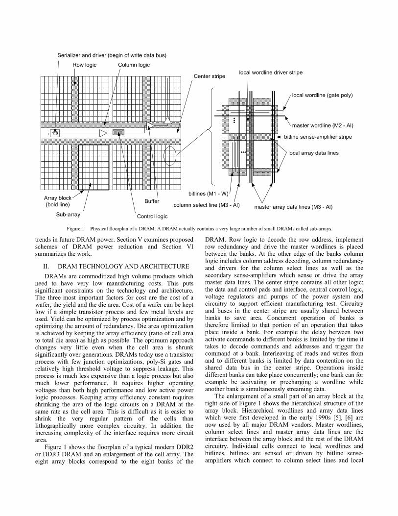
Figure 1 shows the floorplan of a typical modern DDR2 or DDR3 DRAM and an enlargement of the cell array. The eight array blocks correspond to the eight banks of the
DRAM. Row logic to decode the row address, implement row redundancy and drive the master wordlines is placed between the banks. At the other edge of the banks column logic includes column address decoding, column redundancy and drivers for the column select lines as well as the secondary sense-amplifiers which sense or drive the array master data lines. The center stripe contains all other logic: the data and control pads and interface, central control logic, voltage regulators and pumps of the power system and circuitry to support efficient manufacturing test. Circuitry and buses in the center stripe are usually shared between banks to save area. Concurrent operation of banks is therefore limited to that portion of an operation that takes place inside a bank. For example the delay between two activate commands to different banks is limited by the time it takes to decode commands and addresses and trigger the command at a bank. Interleaving of reads and writes from and to different banks is limited by data contention on the shared data bus in the center stripe. Operations inside different banks can take place concurrently; one bank can for example be activating or precharging a wordline while another bank is simultaneously streaming data.
The enlargement of a small part of an array block at the right side of Figure 1 shows the hierarchical structure of the array block. Hierarchical wordlines and array data lines which were first developed in the early 1990s [5], [6] are now used by all major DRAM vendors. Master wordlines, column select lines and master array data lines are the interface between the array block and the rest of the DRAM circuitry. Individual cells connect to local wordlines and bitlines, bitlines are sensed or driven by bitline sense-amplifiers which connect to column select lines and local
Row logic Column logic
Serializer and driver (begin of write data bus)
Buffer
1:8
Control logicSub-array
Center stripe
column select line (M3 - Al) master array data lines (M3 - Al)
local array data lines
master wordline (M2 - Al)
local wordline (gate poly)
bitlines (M1 - W)
local wordline driver stripe
bitline sense-amplifier stripe
Array block (bold line)
Figure 1. Physical floorplan of a DRAM. A DRAM actually contains a very large number of small DRAMs called sub-arrays.
array data lines. The circuitry making the connection between local lines and master lines is placed in the local wordline driver stripe and bitline sense-amplifier stripe respectively, so each sub-array (largest contiguous area of cells) has bitline sense-amplifiers and local wordline drivers surrounding it. The size of the blocks is determined by performance requirements and the total density of a memory. Typically local wordlines and bitlines are between 256 cells and 512 cells long while column select lines and master wordlines extend over 16 to 32 sub-arrays.
Due the hierarchical structure a minimum of three metal levels is needed: one for the bitlines, one for the master wordlines and one for the column select lines and master array data lines. The local wordlines are the gates of the cell access transistors and not an extra metal level. The bitlines are typically tungsten to fit the cell process. They are therefore highly resistive and can be used only for local wiring. Many DRAMs do not use more than the minimum three metal levels to save cost. The exceptions are high performance DRAMs where a fourth metal level for power wiring is less expensive than the area increase that would result from using the existing metal levels and mobile DRAMs which have edge pads to which the data have to be wired from the center stripe.
Access latency and maximum operating frequency is mainly determined by the RC time constants in the array block and to a lesser degree by the circuits in the center stripe. Maximum frequency is limited by the load and therefore length of the master array data lines and column select lines. First access to a page is limited by the load and length of the master and local wordlines and by the speed of sensing data on the bitlines.
The DRAM architecture shown in Figure 1 corresponds to a typical commodity DRAM. Different architectures have been proposed over the years to optimize a DRAM for other applications than main memory. These optimizations always yield a higher cost per bit, which may be acceptable for this application. High performance DRAMs are optimized for maximum total data rate. Their architecture is much more partitioned (e.g. 32 array blocks instead of 8 as shown in Figure 1 for a 1Gb die) to achieve a higher data rate from a larger number of array blocks. Examples of this architecture are GDDR5 [7] and XDR™ DRAM. Mobile DRAMs are optimized for low standby current with data rates similar to commodity DRAMs. Their architecture, e.g. for LP-DDR2 [8] is therefore also more similar to the commodity DRAM architecture but places I/O pads at the chip edge to satisfy the packaging requirements needed to fit in small mobile devices like cell phones. The optimization for low standby current is not visible in the global architecture but influences technology and circuit optimization to reduce leakage current as much as possible. Other ideas for changing the DRAM architecture have so far not been commercially successful.
The main trade-off when deciding on DRAM architecture is cost. Most costly are changes in the bitline sense-amplifier stripe, then in the local wordline driver stripe, then in the column logic and finally in the row logic and center stripe due to the number and size of each of these building blocks in a typical DRAM. DRAM circuitry can be
categorized as on-pitch, i.e. each circuit block is laid out on a pitch corresponding to a small multiple of the bitline or wordline repeat distance and off-pitch, i.e. the circuits are laid out in an area which is not directly corresponding to bitlines or wordlines. Bitline sense-amplifier stripes, local wordline driver stripes and the parts of the row and column logic which are closest to array blocks need to be done on-pitch while the rest of the circuitry is off-pitch. Typically on-pitch circuitry is limited by the size and number of the transistors used to implement a function while off-pitch circuitry is limited by the amount of signal and power wiring needed due to the low number of metal layers. These limitations need to be considered when evaluating architecture modifications. A typical bitline sense-amplifier stripe has 11 transistors per bitline pair (Figure 2), a typical local wordline driver stripe has 3 transistors per local wordline (Figure 3). The share of bitline sense-amplifier area to total die area in a typical commodity DRAM is between 8% and 15%, the share of local wordline driver area is between 5% and 10%. These numbers show why adding even simple functionality in these stripes will have significant area impact. Even worse is the impact of changes which double the number of these blocks e.g. to achieve higher performance with shorter wires. In contrast adding functionality to off-pitch circuits in the center stripe will have little area impact as long as the number of signals is not significantly increased.
III. POWER MODEL
A. General Approach Like all CMOS devices, operating a DRAM requires
charging and discharging transistor gates as well as signal wires connecting transistor gates and junctions. DRAMs are operated at the RC limit of individual switching processes. There are therefore no adiabatic energy savings except for the bitline precharge to midlevel which is achieved by shorting true and complement bitline. The inductance of the internal wiring can be neglected as the resistance is high and the switching frequency is low relative to the size of the inductance. The dissipated energy when charging and discharging a capacitance C to voltage V is therefore approximately
2
21 CV=ε
. (1)
The total power usage of a DRAM is then the sum over all charging and discharging events multiplied with their respective frequency of occurrence
∑= iii fVCP 2
21
. (2)
According to this equation, the DRAM operation is partitioned in the power model into a large number of charge and discharge processes for which capacitance, voltage and
frequency can be determined individually, and the total power is calculated by summing up the contributions.
DRAMs have four main voltage domains: wordlines are boosted above Vdd (Vpp domain) to allow sufficient write-back through the low leakage and high threshold voltage NMOS array transistors. The voltage written back into the cell is the bitline voltage, Vbl, and is determined by the reliability limited maximum voltage which can be stored in the cell capacitor. The voltage Vint supplying most of the circuitry is in some DRAMs regulated from the external voltage Vdd; in other DRAMs it is directly connected to it. The last voltage domain is the external voltage Vdd itself which supplies part of the interface circuitry and the charge pumps and generators creating the derived voltages. In the model, other internal voltages which draw very little current (e.g. the plate voltage at the common node of the cell
capacitor or the well bias in the array) are ignored. Also ignored is the interface signaling voltage Vddq as the power in this voltage domain is not included in DRAM datasheet power values and has to be calculated based on the properties of the link between DRAM and controller, not based on the DRAM itself.
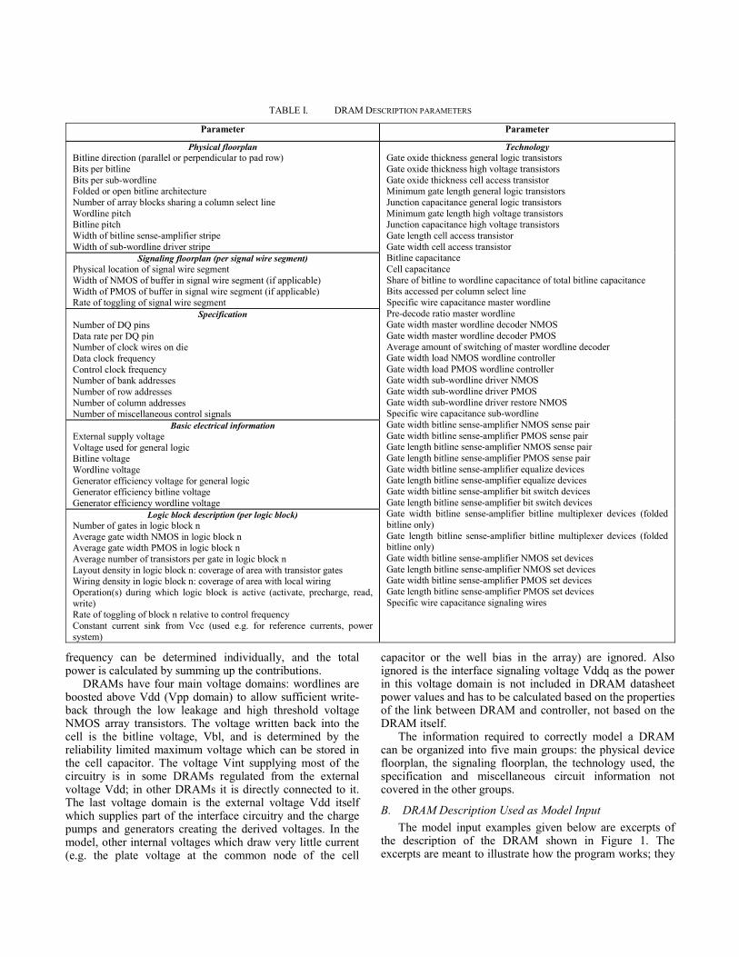
The information required to correctly model a DRAM can be organized into five main groups: the physical device floorplan, the signaling floorplan, the technology used, the specification and miscellaneous circuit information not covered in the other groups.
B. DRAM Description Used as Model Input The model input examples given below are excerpts of
the description of the DRAM shown in Figure 1. The excerpts are meant to illustrate how the program works; they
TABLE I. DRAM DESCRIPTION PARAMETERS
Parameter Parameter
Physical floorplan Bitline direction (parallel or perpendicular to pad row) Bits per bitline Bits per sub-wordline Folded or open bitline architecture Number of array blocks sharing a column select line Wordline pitch Bitline pitch Width of bitline sense-amplifier stripe Width of sub-wordline driver stripe
Technology Gate oxide thickness general logic transistors Gate oxide thickness high voltage transistors Gate oxide thickness cell access transistor Minimum gate length general logic transistors Junction capacitance general logic transistors Minimum gate length high voltage transistors Junction capacitance high voltage transistors Gate length cell access transistor Gate width cell access transistor Bitline capacitance Cell capacitance Share of bitline to wordline capacitance of total bitline capacitance Bits accessed per column select line Specific wire capacitance master wordline Pre-decode ratio master wordline Gate width master wordline decoder NMOS Gate width master wordline decoder PMOS Average amount of switching of master wordline decoder Gate width load NMOS wordline controller Gate width load PMOS wordline controller Gate width sub-wordline driver NMOS Gate width sub-wordline driver PMOS Gate width sub-wordline driver restore NMOS Specific wire capacitance sub-wordline Gate width bitline sense-amplifier NMOS sense pair Gate width bitline sense-amplifier PMOS sense pair Gate length bitline sense-amplifier NMOS sense pair Gate length bitline sense-amplifier PMOS sense pair Gate width bitline sense-amplifier equalize devices Gate length bitline sense-amplifier equalize devices Gate width bitline sense-amplifier bit switch devices Gate length bitline sense-amplifier bit switch devices Gate width bitline sense-amplifier bitline multiplexer devices (folded bitline only) Gate length bitline sense-amplifier bitline multiplexer devices (folded bitline only) Gate width bitline sense-amplifier NMOS set devices Gate length bitline sense-amplifier NMOS set devices Gate width bitline sense-amplifier PMOS set devices Gate length bitline sense-amplifier PMOS set devices Specific wire capacitance signaling wires
Signaling floorplan (per signal wire segment) Physical location of signal wire segment Width of NMOS of buffer in signal wire segment (if applicable) Width of PMOS of buffer in signal wire segment (if applicable) Rate of toggling of signal wire segment
Specification Number of DQ pins Data rate per DQ pin Number of clock wires on die Data clock frequency Control clock frequency Number of bank addresses Number of row addresses Number of column addresses Number of miscellaneous control signals
Basic electrical information External supply voltage Voltage used for general logic Bitline voltage Wordline voltage Generator efficiency voltage for general logic Generator efficiency bitline voltage Generator efficiency wordline voltage
Logic block description (per logic block) Number of gates in logic block n Average gate width NMOS in logic block n Average gate width PMOS in logic block n Average number of transistors per gate in logic block n Layout density in logic block n: coverage of area with transistor gates Wiring density in logic block n: coverage of area with local wiring Operation(s) during which logic block is active (activate, precharge, read, write) Rate of toggling of block n relative to control frequency Constant current sink from Vcc (used e.g. for reference currents, power system)
do not constitute the full input file. The full list of parameters is given in Table I.
1) Physical Floorplan The power model proposed here requires a description of
the DRAM architecture as outlined in Section II and shown in Figure 1. The model calculates the size of the array blocks from the bitline pitch, wordline pitch and the width of bitline sense-amplifier and local wordline driver stripes. Other blocks are described by their orientation and width. The DRAM floorplan is then given by describing the arrangement of blocks along both axes.
An excerpt of the input language describing the physical floorplan is
FloorplanPhysical CellArray BL=v BitsPerBL=512 BLtype=open CellArray WLpitch=165nm BLpitch=110nm Vertical blocks = A1 P1 P2 P1 A1 SizeVertical A1=3396um P1=200um P2=530um
This excerpt describes a cross-cut of the sample DRAM in vertical (y-direction). There is an array block (A1) at the bottom and top and two types of peripheral circuitry, one of which is instantiated twice. In addition physical dimensions are given.
The description of the physical floorplan establishes a coordinate system, in case of the sample DRAM the blocks are numbered 0 to 6 in horizontal (x-) direction and 0 to 4 in vertical (y-) direction.
2) Signaling Floorplan A significant portion of DRAM power is used to charge
and discharge the capacitance of long signaling wires. Quite often these wires interrupted either by buffers to re-drive them or multiplexers to switch their connections to other parts of the DRAM. In the model the main busses (read and write data bus, bank, row and column address bus, control bus and the clock) are built from wire segments with optional device loads inserted in the bus.
Figure 1 shows, in addition to the physical floorplan, the write data bus of a typical DDR3 DRAM as an example. Data from the I/O pad are de-serialized from the high interface speed to the low core speed (1:8 in case of DDR3). They are then driven along the center stripe to a bank typically with re-drivers and / or multiplexers inserted along the path and then driven inside the column stripe to the master array data lines which connect them to the local array data lines and bitlines.
Using the coordinate system described above the write data bus shown has an 1:8 de-serializer in block (0,2), a re-driver in block (2,2), two more re-drivers / multiplexers in
blocks (5,3) and (6,3) and the final data wire extends across block (6,4). The input language excerpt below shows part of that description
FloorplanSignaling DataW0 inside=0_2 fraction=25% dir=h mux=1:8 DataW1 start=0_2 end=3_2 PchW=19.2 NchW=9.6
Signal segments from one block to another are assumed to extend from block center to block center, segments inside one block need to have their relative length with respect to the block and their direction defined. For each segment of each signal the associated wire and device capacitances are calculated. Wire capacitance is modeled by multiplying the wire length with a specific capacitance per unit length and device capacitance is determined by gate capacitance, calculated from gate area and equivalent dielectric thickness as well as junction capacitance calculated from junction width and specific junction capacitance per width. These parameters have to be provided as part of the technology description.
3) Technology DRAM power is strongly dependent on the technology
used to manufacture the DRAM. The internal voltages Vpp, Vbl and Vint are determined by the technology and are lower in advanced technologies. The devices in the sense-amplifier (NMOS and PMOS sense pair, equalize, bit switch and in case of a folded bitline the bitline multiplexers) are defined by their width and length.
The same input is given for the main devices of the row circuitry in the array block: the sub-wordline driver n- and p-channel device and the wordline restore device of the sub-wordline driver and decoder and the pull-down of the master wordline decoder. As described above, device loads are calculated as the sum of gate and junction capacitance. In addition the cell capacitance, the bitline capacitance and the share of the bitline capacitance which couples to the wordline needs to be defined.
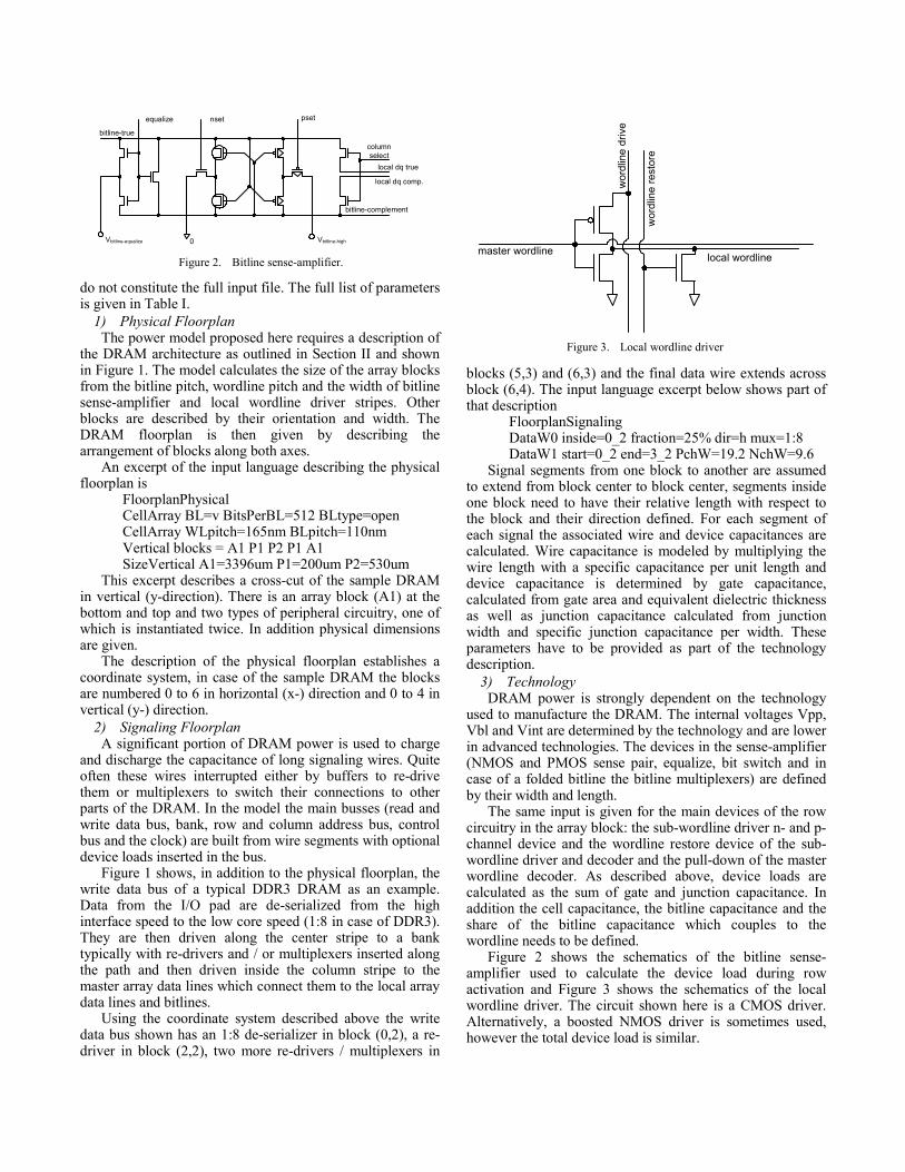
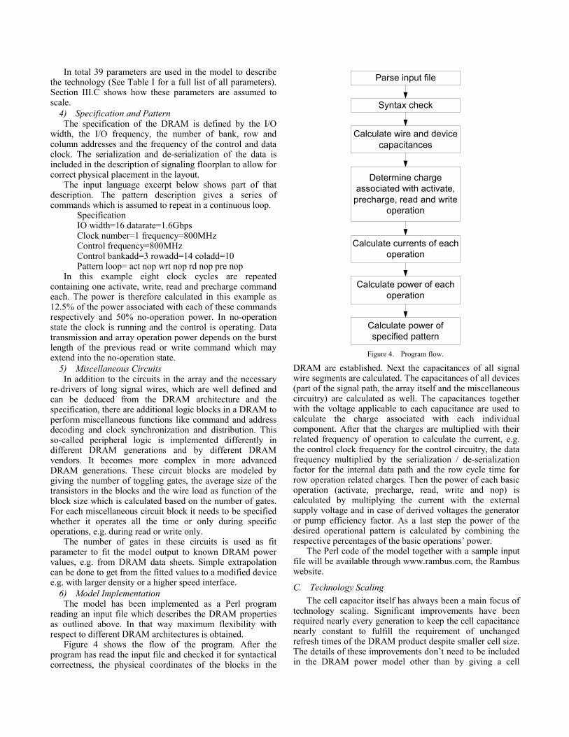
Figure 2 shows the schematics of the bitline sense-amplifier used to calculate the device load during row activation and Figure 3 shows the schematics of the local wordline driver. The circuit shown here is a CMOS driver. Alternatively, a boosted NMOS driver is sometimes used, however the total device load is similar.
0 Vbitline-high
column select
local dq true
local dq comp.
bitline-complement
bitline-true
equalize nset pset
Vbitline-equalize Figure 2. Bitline sense-amplifier.
master wordline local wordline
wor
dlin
e dr
ive
wor
dlin
e re
stor
e
Figure 3. Local wordline driver
In total 39 parameters are used in the model to describe the technology (See Table I for a full list of all parameters). Section III.C shows how these parameters are assumed to scale.
4) Specification and Pattern The specification of the DRAM is defined by the I/O
width, the I/O frequency, the number of bank, row and column addresses and the frequency of the control and data clock. The serialization and de-serialization of the data is included in the description of signaling floorplan to allow for correct physical placement in the layout.
The input language excerpt below shows part of that description. The pattern description gives a series of commands which is assumed to repeat in a continuous loop.
Specification IO width=16 datarate=1.6Gbps Clock number=1 frequency=800MHz Control frequency=800MHz Control bankadd=3 rowadd=14 coladd=10 Pattern loop= act nop wrt nop rd nop pre nop
In this example eight clock cycles are repeated containing one activate, write, read and precharge command each. The power is therefore calculated in this example as 12.5% of the power associated with each of these commands respectively and 50% no-operation power. In no-operation state the clock is running and the control is operating. Data transmission and array operation power depends on the burst length of the previous read or write command which may extend into the no-operation state.
5) Miscellaneous Circuits In addition to the circuits in the array and the necessary
re-drivers of long signal wires, which are well defined and can be deduced from the DRAM architecture and the specification, there are additional logic blocks in a DRAM to perform miscellaneous functions like command and address decoding and clock synchronization and distribution. This so-called peripheral logic is implemented differently in different DRAM generations and by different DRAM vendors. It becomes more complex in more advanced DRAM generations. These circuit blocks are modeled by giving the number of toggling gates, the average size of the transistors in the blocks and the wire load as function of the block size which is calculated based on the number of gates. For each miscellaneous circuit block it needs to be specified whether it operates all the time or only during specific operations, e.g. during read or write only.
The number of gates in these circuits is used as fit parameter to fit the model output to known DRAM power values, e.g. from DRAM data sheets. Simple extrapolation can be done to get from the fitted values to a modified device e.g. with larger density or a higher speed interface.
6) Model Implementation The model has been implemented as a Perl program
reading an input file which describes the DRAM properties as outlined above. In that way maximum flexibility with respect to different DRAM architectures is obtained.
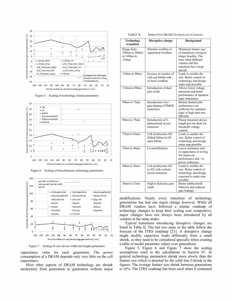
Figure 4 shows the flow of the program. After the program has read the input file and checked it for syntactical correctness, the physical coordinates of the blocks in the
DRAM are established. Next the capacitances of all signal wire segments are calculated. The capacitances of all devices (part of the signal path, the array itself and the miscellaneous circuitry) are calculated as well. The capacitances together with the voltage applicable to each capacitance are used to calculate the charge associated with each individual component. After that the charges are multiplied with their related frequency of operation to calculate the current, e.g. the control clock frequency for the control circuitry, the data frequency multiplied by the serialization / de-serialization factor for the internal data path and the row cycle time for row operation related charges. Then the power of each basic operation (activate, precharge, read, write and nop) is calculated by multiplying the current with the external supply voltage and in case of derived voltages the generator or pump efficiency factor. As a last step the power of the desired operational pattern is calculated by combining the respective percentages of the basic operations’ power.
The Perl code of the model together with a sample input file will be available through www.rambus.com, the Rambus website.
C. Technology Scaling The cell capacitor itself has always been a main focus of
technology scaling. Significant improvements have been required nearly every generation to keep the cell capacitance nearly constant to fulfill the requirement of unchanged refresh times of the DRAM product despite smaller cell size. The details of these improvements don’t need to be included in the DRAM power model other than by giving a cell
Parse input file
Syntax check
Calculate wire and device capacitances
Determine charge associated with activate,
precharge, read and write operation
Calculate currents of each operation
Calculate power of each operation
Calculate power of specified pattern
Figure 4. Program flow.
capacitance value for each generation. The power consumption of a DRAM depends only very little on the cell capacitance.
Most other aspects of DRAM technology are shrunk moderately from generation to generation without major
modifications. Nearly every transition of technology generations has had one major change however. While all DRAM vendors have followed a similar roadmap of technology changes to keep their scaling cost competitive, major changes have not always been introduced by all vendors at the same nodes.
Typical transitions introducing disruptive changes are listed in Table II. The last two steps in the table follow the forecast of the ITRS roadmap [21]. A disruptive change might modify capacitive loads differently from a small shrink, so they need to be considered specially when creating a table of model parameter values over generations.
Figure 5, Figure 6 and Figure 7 show the scaling assumptions used in the calculations in Section IV. In general technology parameters shrink more slowly than the feature size which is denoted by the solid line f-shrink in the figures. The average feature size shrink between generations is 16%. The ITRS roadmap has been used when it contained
Figure 5. Scaling of technology related parameters
Figure 6. Scaling of miscellaneous technology parameters
Figure 7. Scaling of core device width and length parameters
TABLE II. DISRUPTIVE DRAM TECHNOLOGY CHANGES
Technology transition
Disruptive change Background
Range from 250nm to 200nm to 140nm to 110nm
Stitched wordline to segmented wordline
Minimum feature size of aluminum wiring no longer feasible. The time when different vendors did this transition has a large spread
110nm to 90nm Increase in number of cells per bitline and / or local wordline
Leads to smaller die size. Better control of technology and design make step possible.
110nm to 90nm Introduction of dual gate oxide
Allows lower voltage operation and better performance of standard logic transistors.
90nm to 75nm Introduction of p+ gate doping of PMOS transistors
Buried channel pfet performance not sufficient for standard logic of high data rate DRAMs.
90nm to 75nm Introduction of 3-dimensional access transistor
Planar transistor device length got too short for threshold voltage control.
75nm to 65nm Cell architecture 8f2 folded bitline to 6f2 open bitline
Leads to smaller die size. Better control of technology and design make step possible.
55nm to 44nm Cu metallization Lower resistance and / or capacitance in wiring for improved performance and / or power reduction.
40nm to 36nm Cell architecture 6f2 to 4f2 with vertical access transistor
Leads to smaller die size. Better control of technology and design expected to make step possible.
36nm to 31nm High-k dielectric gate oxide
Better subthreshold behavior and reduced gate leakage.
information on a specific parameter. When this was not the case a moderate shrink factor was assumed. Transistor sizes were generally scaled by scaling length following the feature size and keeping the width over length ratio constant.
Figure 5 shows the shrink factor of gate oxide thicknesses, minimum channel length, junction capacitance and access transistor length and width following the ITRS roadmap if applicable.
Figure 6 shows the shrink factor for bitline and cell capacitance, the average width of miscellaneous logic devices and the width of the sense-amplifier stripe respectively the local wordline driver stripe. The width of the transistors driving long wire load is assumed to follow the minimum channel length to keep the length over width ratio constant and Figure 7 describes the shrink factor of the transistors in the bitline sense-amplifier and the on-pitch row circuitry.
IV. APPLICATION
A. Verification Against Data Sheets The DRAM power model has been compared to DRAM
power data from data sheets and publications both to verify its accuracy and to fit the parameters describing the miscellaneous circuitry. Figure 8 and Figure 9 show the comparison of currents calculated with the model to data sheet values from major DRAM vendors [22], [23]. As expected the data sheet value show a quite large spread. This is due to the different technologies used to build the DRAMs and differences in the power efficiencies of the approach used by different DRAM vendors.
DRAM feature and die size, circuit design and internal voltages vary considerably between vendors and between technology generations of the same vendor. The model values have been calculated for a typical 75nm and 65nm technology in the case of DDR2 and a typical 65nm and 55nm technology in the case of DDR3. Assumptions used in technology scaling have been explained in Section III.C. DRAM vendors normally do not publish the technology node of a DRAM in their data sheets, so the comparison assumed technology nodes which were typically used for high volume parts in the time frame the DRAMs used in the comparison were on the market.
The figures show good agreement between data sheet current values and the model. The dependency of current on operating frequency, interface standard, I/O width and type of operation (Idd0 is row operation, Idd4R and Idd4W are read and write operation respectively) is described correctly. The labels on the x-axis describe the point of comparison, e.g. Idd0 533 x4 is the Idd0 of a part with 4 bits I/O width and 533Mbit/s/pin data rate.
B. Power Consumption Pareto Unlike a power model based on data sheet values only
the model described here allows independent variation of all contributors to power consumption of a DRAM. It is therefore possible to rank all the parameters by their impact on the total power consumption. The DRAM power model described in this work has a very large number of
parameters, so it is important to see which ones are influencing power most not only to learn where power can be saved but also which parameters need to be understood well to have an accurate model.
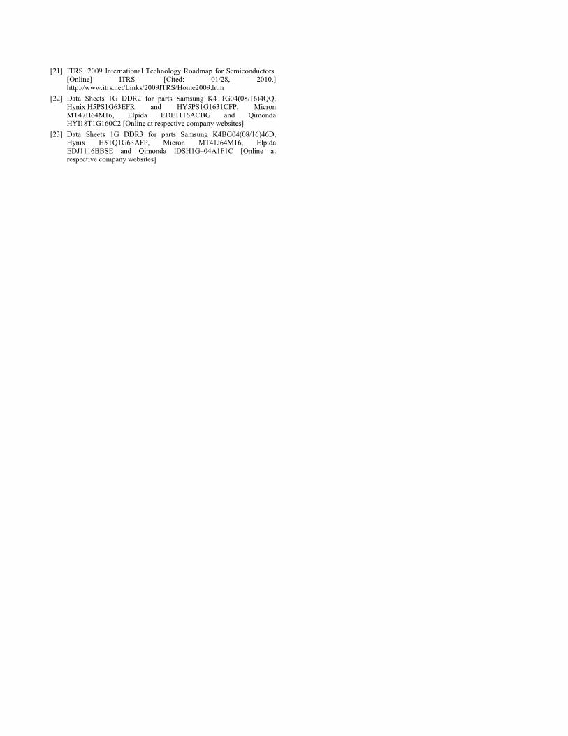
Figure 10 shows the change in power consumption as function of a parameter change by ±20% sorted by the impact on a 1G DDR3 DRAM in a 55nm technology. The
Figure 8. Comparison of model to datasheet for 1G DDR2
Figure 9. Comparison of model to datasheet for 1G DDR3
Figure 10. Change in power consumption dependent on parameter variation
two other DRAMs shown are a 128M SDR DRAM in a 170nm technology and a hypothetical 16G DDR5 DRAM in an 18nm technology. Section IV.C has more details on the definition of these devices. The pattern used in this comparison is a pattern with activate and precharge as well as read and write operation (equivalent to an Idd7 pattern but with half of the read operations replaced by write operations).
A variation of 40% would mean that the power consumption is directly proportional to the value of the varied parameter. This is only the case for the external supply voltage Vdd which is not shown in the chart. Internal voltages in the DRAM are modeled as being derived from the external voltage with an efficiency factor to account for the pump or generator which might be used. Sensitivity to the type of internal supply will therefore not show up in the Pareto at the external voltage but at the internal voltage itself and the efficiency factor. All other parameters influence only part of the power consumption and show therefore smaller variation. Most parameters have little individual influence; only their overall contribution is determining power consumption. Table III shows the top ten parameters of each of the three sample DRAMs of different generations spanning the years from approximately 2000 to approximately 2017. Comparing the different DRAM generations shows a shift from direct array related power consumption to signal wiring and logic circuitry power consumption as the most important contributors to overall power consumption. Within the circuitry importance shifts from transistor related parameters, e.g. oxide thickness to wiring capacitance. The bandwidth changes much more between SDR and DDR5 than the basic array architecture and internal operation frequency. This shifts the share of power from the activate and precharge operation (row or page access operation) to the read and write operation
(column operation) and is mainly responsible for the growing importance of wiring and logic circuitry.
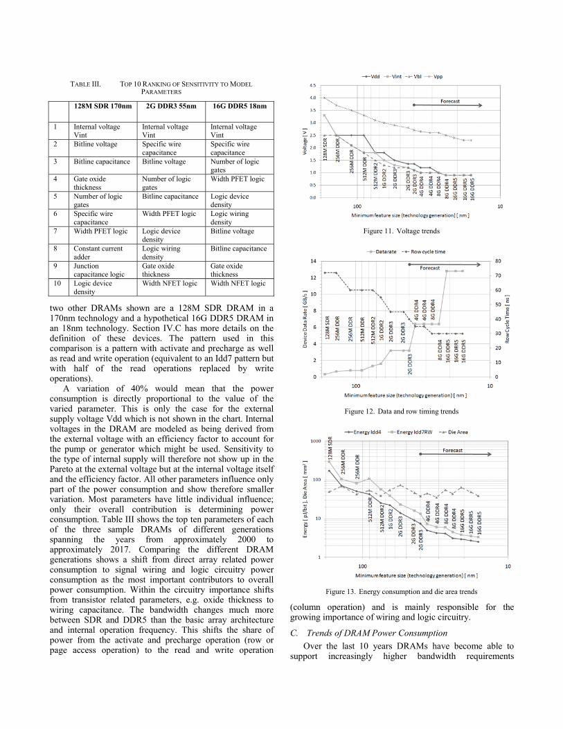
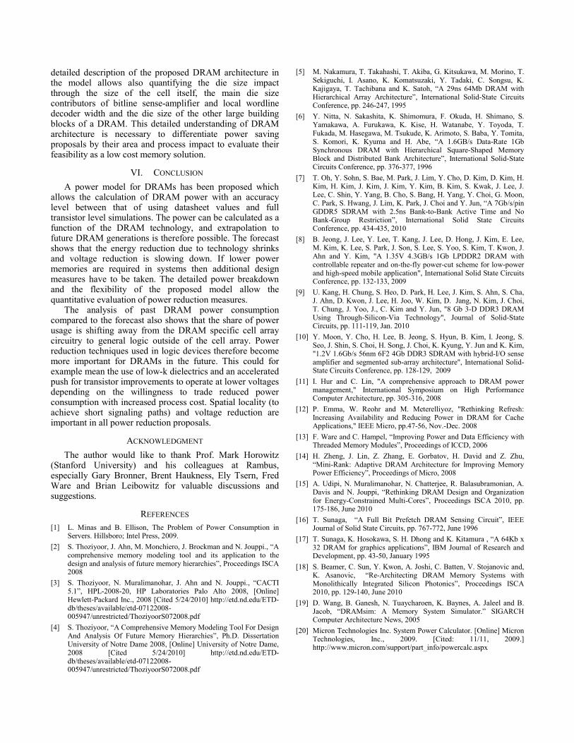
C. Trends of DRAM Power Consumption Over the last 10 years DRAMs have become able to
support increasingly higher bandwidth requirements
Figure 11. Voltage trends
Figure 12. Data and row timing trends
Figure 13. Energy consumption and die area trends
TABLE III. TOP 10 RANKING OF SENSITIVITY TO MODEL PARAMETERS
128M SDR 170nm 2G DDR3 55nm 16G DDR5 18nm
1 Internal voltage Vint
Internal voltage Vint
Internal voltage Vint
2 Bitline voltage Specific wire capacitance
Specific wire capacitance
3 Bitline capacitance Bitline voltage Number of logic gates
4 Gate oxide thickness
Number of logic gates
Width PFET logic
5 Number of logic gates
Bitline capacitance Logic device density
6 Specific wire capacitance
Width PFET logic Logic wiring density
7 Width PFET logic Logic device density
Bitline voltage
8 Constant current adder
Logic wiring density
Bitline capacitance
9 Junction capacitance logic
Gate oxide thickness
Gate oxide thickness
10 Logic device density
Width NFET logic Width NFET logic
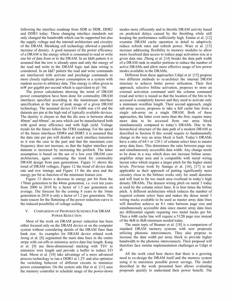
following the interface roadmap from SDR to DDR, DDR2 and DDR3 today. These changing interface standards not only changed the bandwidth which can be supported but also the supply voltage and the internal architecture and circuitry of the DRAM. Shrinking cell technology allowed a parallel increase of density. A good measure of the power efficiency of a DRAM is the energy which is consumed to read or write one bit of data from or to the DRAM. In an Idd4 pattern it is assumed that the row is already open and only the energy of the read and write in the DRAM logic and data wiring is considered. In an Idd7 pattern the read and write commands are interleaved with activate and precharge commands to more closely replicate power consumption in a system with random access to arbitrary data. This energy is often given in mW per gigabit per second which is equivalent to pJ / bit.
The power calculations showing the trend of DRAM power consumption have been done for commodity DRAM interfaces specified according to the mainstream interface specification at the time of peak usage of a given DRAM technology. The assumed device I/O width was x16 and the datarate per pin at the high end of typically available devices. The density is chosen so that the die area is between about 40mm2 and 60mm2, an area which can be manufactured both with good array efficiency and with high yield. Voltage trends for the future follow the ITRS roadmap. For the speed of the future interfaces DDR4 and DDR5 it is assumed that the data rate per pin will double at each interface transition as it was the case in the past and that the maximum core frequency does not increase, so that the higher interface pin datarate is increased by increasing the prefetch. The latter assumption is based on the use of a low cost DRAM core architecture, again continuing the trend for commodity DRAM design from past generations. Figure 11 shows the trend of DRAM voltages, Figure 12 the trend of device data rate and row timings and Figure 13 the die area and the energy per bit as function of the minimum feature size.
Figure 13 shows a decrease in energy per bit from the 170nm generation to the 44nm generation, i.e. over ten years from 2000 to 2010 by a factor of 1.5 per generation on average. The forecast for the coming 8 years to the 16nm generation in 2018 is only a factor of 1.2 per generation. The main reason for the flattening of the power reduction curve is the reduced possibility of voltage scaling.
V. COMPARISON OF PROPOSED SCHEMES FOR DRAM POWER REDUCTION
Most of the work on DRAM power reduction has been either focused only on the DRAM device or on the computer system without considering details of the DRAM finer than bank size. As examples for DRAM device related work Jeong et al. [8] segmented the main data lines in the centre stripe with cut-offs to minimize active data line length. Kang et al. [9] use three-dimensional stacking with TSV to minimize wire length and provide a buffer to reduce I/O load. Moon et al. [10] take advantage of a more advanced process technology to run a DDR3 at 1.2V and also optimize the switching behavior of different circuits to minimize power consumption. On the system side Hur et al. [11] uses the memory controller to schedule usage of the power-down
modes more efficiently and to throttle DRAM activity based on predicted delays caused by the throttling while still keeping the performance sufficiently high. Emma et al. [12] examine DRAM cache operation in detail to adaptively reduce refresh rates and refresh power. Ware et al. [13] increase addressing flexibility to memory modules to allow more localized data access to reduce page activation size at a given data rate. Zheng et al. [14] breaks the data path width of a DRAM rank in smaller portions to reduce the number of active DRAMs and allow more effective usage of low power modes available in the DRAMs.
Different from these approaches Udipi et al. [15] propose two different methods to re-architect the internal DRAM structure to achieve better power utilization. Their first approach, selective bitline activation, proposes to store an external activation command until the column command (read and write) is issued so that the location of the bits to be accessed is completely known and they need to activate only a minimum wordline length. Their second approach, single sub-array access, proposes to take a full cache line from a single sub-array on a single DRAM. Both of these approaches, the latter even more than the first, require many more data to be accessed from one array block simultaneously compared to today’s DRAMs. Due to the hierarchical structure of the data path of a modern DRAM as described in Section II this would require to fundamentally change in the way an array block is built. Today’s DRAMs have a ratio of 64:1 or 128:1 of column select lines to master array data lines. This determines the ratio between page size and simultaneously accessible data width. Any change needs to be done in a way which does not increase bitline sense-amplifier stripe area and is compatible with metal wiring layout rules which require a larger pitch for the higher metal levels. Previous work by Sunaga et al. [16], [17] is not applicable as their approach of putting significantly more circuitry close to the bitlines works only for small densities and will lead to far too much area overhead in today’s high density DRAMs. The densest wiring pitch on metal 3 today is used by the column select lines. It is four times the bitline pitch. A different architecture which reduces the number of required column select lines and makes the dense metal 3 wiring tracks available to be used as master array data lines will therefore achieve an 8:1 ratio between page size and simultaneously accessible data since master array data lines are differential signals requiring two metal tracks per bit. Then a 64B cache line will require a 512B page size instead of the 4kB to 8kB minimum needed today.
The main topic of Beamer et al. [18] is a comparison of standard DRAM memory systems with new proposals utilizing photonic interconnects. They also propose to increase the data width per array block to provide higher bandwidth to the photonic interconnects. Their proposal will therefore face similar implementation challenges as Udipi et al.
All the work cited here shows that there is a growing need to co-design the DRAM itself and the memory system using it to maximize possible power savings. The model described in the work presented here allows evaluating proposals quickly to understand their power benefit. The
detailed description of the proposed DRAM architecture in the model allows also quantifying the die size impact through the size of the cell itself, the main die size contributors of bitline sense-amplifier and local wordline decoder width and the die size of the other large building blocks of a DRAM. This detailed understanding of DRAM architecture is necessary to differentiate power saving proposals by their area and process impact to evaluate their feasibility as a low cost memory solution.
VI. CONCLUSION A power model for DRAMs has been proposed which
allows the calculation of DRAM power with an accuracy level between that of using datasheet values and full transistor level simulations. The power can be calculated as a function of the DRAM technology, and extrapolation to future DRAM generations is therefore possible. The forecast shows that the energy reduction due to technology shrinks and voltage reduction is slowing down. If lower power memories are required in systems then additional design measures have to be taken. The detailed power breakdown and the flexibility of the proposed model allow the quantitative evaluation of power reduction measures.
The analysis of past DRAM power consumption compared to the forecast also shows that the share of power usage is shifting away from the DRAM specific cell array circuitry to general logic outside of the cell array. Power reduction techniques used in logic devices therefore become more important for DRAMs in the future. This could for example mean the use of low-k dielectrics and an accelerated push for transistor improvements to operate at lower voltages depending on the willingness to trade reduced power consumption with increased process cost. Spatial locality (to achieve short signaling paths) and voltage reduction are important in all power reduction proposals.
ACKNOWLEDGMENT The author would like to thank Prof. Mark Horowitz
(Stanford University) and his colleagues at Rambus, especially Gary Bronner, Brent Haukness, Ely Tsern, Fred Ware and Brian Leibowitz for valuable discussions and suggestions.
REFERENCES [1] L. Minas and B. Ellison, The Problem of Power Consumption in
Servers. Hillsboro; Intel Press, 2009. [2] S. Thoziyoor, J. Ahn, M. Monchiero, J. Brockman and N. Jouppi., “A
comprehensive memory modeling tool and its application to the design and analysis of future memory hierarchies”, Proceedings ISCA 2008
[3] S. Thoziyoor, N. Muralimanohar, J. Ahn and N. Jouppi., “CACTI 5.1”, HPL-2008-20, HP Laboratories Palo Alto 2008, [Online] Hewlett-Packard Inc., 2008 [Cited 5/24/2010] http://etd.nd.edu/ETD-db/theses/available/etd-07122008-005947/unrestricted/ThoziyoorS072008.pdf
[4] S. Thoziyoor, “A Comprehensive Memory Modeling Tool For Design And Analysis Of Future Memory Hierarchies”, Ph.D. Dissertation University of Notre Dame 2008, [Online] University of Notre Dame, 2008 [Cited 5/24/2010] http://etd.nd.edu/ETD-db/theses/available/etd-07122008-005947/unrestricted/ThoziyoorS072008.pdf
[5] M. Nakamura, T. Takahashi, T. Akiba, G. Kitsukawa, M. Morino, T. Sekiguchi, I. Asano, K. Komatsuzaki, Y. Tadaki, C. Songsu, K. Kajigaya, T. Tachibana and K. Satoh, “A 29ns 64Mb DRAM with Hierarchical Array Architecture”, International Solid-State Circuits Conference, pp. 246-247, 1995
[6] Y. Nitta, N. Sakashita, K. Shimomura, F. Okuda, H. Shimano, S. Yamakawa, A. Furukawa, K. Kise, H. Watanabe, Y. Toyoda, T. Fukada, M. Hasegawa, M. Tsukude, K. Arimoto, S. Baba, Y. Tomita, S. Komori, K. Kyuma and H. Abe, “A 1.6GB/s Data-Rate 1Gb Synchronous DRAM with Hierarchical Square-Shaped Memory Block and Distributed Bank Architecture”, International Solid-State Circuits Conference, pp. 376-377, 1996
[7] T. Oh, Y. Sohn, S. Bae, M. Park, J. Lim, Y. Cho, D. Kim, D. Kim, H. Kim, H. Kim, J. Kim, J. Kim, Y. Kim, B. Kim, S. Kwak, J. Lee, J. Lee, C. Shin, Y. Yang, B. Cho, S. Bang, H. Yang, Y. Choi, G. Moon, C. Park, S. Hwang, J. Lim, K. Park, J. Choi and Y. Jun, “A 7Gb/s/pin GDDR5 SDRAM with 2.5ns Bank-to-Bank Active Time and No Bank-Group Restriction”, International Solid State Circuits Conference, pp. 434-435, 2010
[8] B. Jeong, J. Lee, Y. Lee, T. Kang, J. Lee, D. Hong, J. Kim, E. Lee, M. Kim, K. Lee, S. Park, J. Son, S. Lee, S. Yoo, S. Kim, T. Kwon, J. Ahn and Y. Kim, "A 1.35V 4.3GB/s 1Gb LPDDR2 DRAM with controllable repeater and on-the-fly power-cut scheme for low-power and high-speed mobile application", International Solid State Circuits Conference, pp. 132-133, 2009
[9] U. Kang, H. Chung, S. Heo, D. Park, H. Lee, J. Kim, S. Ahn, S. Cha, J. Ahn, D. Kwon, J. Lee, H. Joo, W. Kim, D. Jang, N. Kim, J. Choi, T. Chung, J. Yoo, J., C. Kim and Y. Jun, "8 Gb 3-D DDR3 DRAM Using Through-Silicon-Via Technology", Journal of Solid-State Circuits, pp. 111-119, Jan. 2010
[10] Y. Moon, Y. Cho, H. Lee, B. Jeong, S. Hyun, B. Kim, I. Jeong, S. Seo, J. Shin, S. Choi, H. Song, J. Choi, K. Kyung, Y. Jun and K. Kim, "1.2V 1.6Gb/s 56nm 6F2 4Gb DDR3 SDRAM with hybrid-I/O sense amplifier and segmented sub-array architecture", International Solid-State Circuits Conference, pp. 128-129, 2009
[11] I. Hur and C. Lin, "A comprehensive approach to DRAM power management," International Symposium on High Performance Computer Architecture, pp. 305-316, 2008
[12] P. Emma, W. Reohr and M. Meterelliyoz, "Rethinking Refresh: Increasing Availability and Reducing Power in DRAM for Cache Applications," IEEE Micro, pp.47-56, Nov.-Dec. 2008
[13] F. Ware and C. Hampel, “Improving Power and Data Efficiency with Threaded Memory Modules”, Proceedings of ICCD, 2006
[14] H. Zheng, J. Lin, Z. Zhang, E. Gorbatov, H. David and Z. Zhu, “Mini-Rank: Adaptive DRAM Architecture for Improving Memory Power Efficiency”, Proceedings of Micro, 2008
[15] A. Udipi, N. Muralimanohar, N. Chatterjee, R. Balasubramonian, A. Davis and N. Jouppi, “Rethinking DRAM Design and Organization for Energy-Constrained Multi-Cores”, Proceedings ISCA 2010, pp. 175-186, June 2010
[16] T. Sunaga, “A Full Bit Prefetch DRAM Sensing Circuit”, IEEE Journal of Solid State Circuits, pp. 767-772, June 1996
[17] T. Sunaga, K. Hosokawa, S. H. Dhong and K. Kitamura , “A 64Kb x 32 DRAM for graphics applications”, IBM Journal of Research and Development, pp. 43-50, January 1995
[18] S. Beamer, C. Sun, Y. Kwon, A. Joshi, C. Batten, V. Stojanovic and, K. Asanovic, “Re-Architecting DRAM Memory Systems with Monolithically Integrated Silicon Photonics”, Proceedings ISCA 2010, pp. 129-140, June 2010
[19] D. Wang, B. Ganesh, N. Tuaycharoen, K. Baynes, A. Jaleel and B. Jacob, “DRAMsim: A Memory System Simulator.” SIGARCH Computer Architecture News, 2005
[20] Micron Technologies Inc. System Power Calculator. [Online] Micron Technologies, Inc., 2009. [Cited: 11/11, 2009.] http://www.micron.com/support/part_info/powercalc.aspx
[21] ITRS. 2009 International Technology Roadmap for Semiconductors. [Online] ITRS. [Cited: 01/28, 2010.] http://www.itrs.net/Links/2009ITRS/Home2009.htm
[22] Data Sheets 1G DDR2 for parts Samsung K4T1G04(08/16)4QQ, Hynix H5PS1G63EFR and HY5PS1G1631CFP, Micron MT47H64M16, Elpida EDE1116ACBG and Qimonda HYI18T1G160C2 [Online at respective company websites]
[23] Data Sheets 1G DDR3 for parts Samsung K4BG04(08/16)46D, Hynix H5TQ1G63AFP, Micron MT41J64M16, Elpida EDJ1116BBSE and Qimonda IDSH1G–04A1F1C [Online at respective company websites]