ultra-high extinction-ratio light modulation by
TRANSCRIPT

DOI: 10.29026/oea.2021.200088
Ultra-high extinction-ratio light modulation byelectrically tunable metasurface using dualepsilon-near-zero resonancesArash Nemati1,2, Qian Wang1, Norman Soo Seng Ang1, Weide Wang1,Minghui Hong2 and Jinghua Teng1*
The lossy nature of indium tin oxide (ITO) at epsilon-near-zero (ENZ) wavelength is used to design an electrically tun-able metasurface absorber. The metasurface unit cell is constructed of a circular resonator comprising two ITO discs anda high dielectric constant perovskite barium strontium titanate (BST) film. The ENZ wavelength in the accumulation anddepletion layers of ITO discs is controlled by applying a single bias voltage. The coupling of magnetic dipole resonancewith the ENZ wavelength inside the accumulation layer of ITO film causes total absorption of reflected light. The reflec-tion amplitude can achieve ~84 dB or ~99.99% modulation depth in the operation wavelength of 820 nm at a bias voltageof −2.5 V. Moreover, the metasurface is insensitive to the polarization of the incident light due to the circular design ofresonators and the symmetrical design of bias connections.
Keywords: metasurface; electrically tunable; indium tin oxide (ITO); epsilon-near-zero (ENZ); barium strontium titanate(BST); polarization-insensitive
Nemati A, Wang Q, Ang NSS, Wang WD, Hong MH et al. Ultra-high extinction-ratio light modulation by electrically tunablemetasurface using dual epsilon-near-zero resonances. Opto-Electron Adv 4, 200088 (2021).
IntroductionMetasurfaces are the two-dimensional equivalent ofmetamaterials, composing discrete subwavelength struc-tures, possessing the capability of full control of lightproperties, such as amplitude, phase, dispersion, mo-mentum, and polarization1−7. Metasurfaces are used invarious applications covering electromagnetic spectraranging from microwave, terahertz (THz), infrared, vis-ible, to ultra-violet (UV)8. Active control of lightpropagation in visible and near-infrared (near-IR) spec-tra has practical and fundamental significance in
autonomous vehicles, robots, display, augmented andvirtual reality, consumer electronics, telecommunica-tions, and sensing devices9−14. To tune a metasurface, wecan change either the property of the unit cells or its am-bient. This could be done by employing active materialsin the metasurface, which can have their propertieschanged by an external stimulus. Each type of these ma-terials has different properties and tuning mechanisms.
Transparent conductive oxides are optically transpar-ent and electrically conductive. They have been widelyused in photovoltaics, organic light-emitting diodes,
1Institute of Materials Research and Engineering, Agency for Science, Technology and Research (A*STAR), 2 Fusionopolis Way, Singapore
138634, Singapore; 2Department of Electrical and Computer Engineering, National University of Singapore, Engineering Drive 3, Singapore
117576, Singapore.*Correspondence: JH Teng, Email: [email protected]: 5 December 2020; Accepted: 25 March 2021; Published: 25 July 2021
Opto-Electronic Advances
Original Article2021, Vol. 4, No. 7
Open Access This article is licensed under a Creative Commons Attribution 4.0 International License.To view a copy of this license, visit http://creativecommons.org/licenses/by/4.0/.
© The Author(s) 2021. Published by Institute of Optics and Electronics, Chinese Academy of Sciences.
200088-1

displays, and electro-optics devices15,16. Recently, the tun-able property of transparent conductive oxides, such asindium tin oxide (ITO), has attracted great attention forits applications in metasurfaces and flat optics17.Moreover, the tunability in ITO is a field-effect modula-tion mechanism that is based on the formation of chargedepletion or accumulation regions. This gives them ad-vantages of low power and high speed compared to theother common tuning mechanisms, such as MEMS,mechanical strain, liquid crystals, and phase change ma-terials9,18−20.
So far most of the focus in using tunable ITO film hasbeen on designing beamsteering metasurfaces21−23. Totune the electron density and optical constants in theITO film, different structures have been proposed. A300° phase change was shown in a reflective dual-gatemetasurface structure using a single ITO film with themeasured reflectance below 30%22. Recently, over 360°phase change and a scan angle of 8° with a deflection effi-ciency of 34% were achieved24. Although the strong res-onance and electric and magnetic confinement in theITO film has been very beneficial to achieving high phasechange, it has limited the achievable efficiency.
Hence, ITO could be a better candidate for modula-tion of light intensity by playing with its plasmonic res-onance. An electrically tunable metasurface working as amodulator could not only benefit from the fast tunabil-ity of ITO but also the compactness of metasurfacedesign. Different structures have been proposed so far toanswer such demand. Placing an ITO film inside a met-al-insulator-metal (MIM) plasmonic cavity, a tunable re-flective absorber with up to 15% change in amplitude ofreflected light was achieved25. A broadband electro-optic-al modulator based on a multilayer structure was able toattain 37% modulation depth for the reflected light whenthe incoming light has a 78° incidence angle26. A high-ef-ficiency transmittance modulator using ITO-basedmetasurfaces and hybrid plasmonic waveguide mode hasshown a 33% gate-tunable transmittance change by ap-plying a 6 V gate bias27. An all-dielectric Huygens metas-urface was proposed to control the transmission of lightwith an on-state transmittance of 70% and a modulationdepth of 31%28. Moreover, a circular MIM resonator withan ITO film that is polarization insensitive could realizethe modulation of transmitted light with a large modula-tion depth up to 29 dB or 96%29. However, all of thesemetasurfaces comprise a single ITO film with limitedmodulation depth and their operational wavelength was
also restricted to λ ≥ ~1500 nm in the near-IR spectrumdue to the low electron concentration of the depositedITO film.
V = −2.5
Here, a new circular resonator comprising two ITOdiscs is proposed. We use the coupling of magnetic di-pole resonance in the circular resonator with the ENZwavelength inside the accumulation layer of ITO film toachieve total absorption of reflected light. This is mainlydue to the coexistence of magnetic dipole resonance andENZ wavelength inside the ITO discs. A perovskite highdielectric constant barium strontium titanate (BST) filmis sandwiched between two ITO films to increase theelectric field and decrease the required voltage. An un-precedented ~84 dB or ~99.99% modulation depth in thereflection mode, insensitive to the polarization of light,was achieved at λ = 820 nm with a single bias voltage of
V. The results show a promising way for real-izing electrically tunable metasurface for potential high-speed light modulation.
Methods and resultsITO is a conducting material with free electrons which isoptically modeled using the Drude model in the visibleand near-IR spectra30:
εr (ω) = ε′r (ω) + iε′′r (ω) = ε∞ −ω2
p
ω2 + iωΓ, (1)
εr ε′r ε′′rε∞
ωωp Γ
where is the material permittivity, and are the realand imaginary parts of the permittivity respectively, isthe high-frequency permittivity, is the angular fre-quency, is the plasma frequency, and is the damp-ing rate. The plasma frequency and damping rate aredefined as:
ω2p =
Ne2
ε0m∗ , (2)
Γ =1τ=
eμm∗ , (3)
τ e με0 m∗
N
where is scattering time, is the electron charge, isthe electron mobility, is the vacuum permittivity, isthe effective electron mass, and is the electron concen-tration. By changing the carrier concentration, theplasma frequency changes, thereby changing the dielec-tric constant. From Eq. (1), the real and imaginary partsof the permittivity are given by:
ε′r (ω) = ε∞ −ω2
p
ω2 + Γ2, (4)
Opto-Electron Adv 4, 200088 (2021) https://doi.org/10.29026/oea.2021.200088
200088-2

ε′′r (ω) =Γω2
p
ω (ω2 + Γ2). (5)
λENZ
εr = 0
λENZ
The epsilon-near-zero (ENZ) wavelength ( ) is thewavelength at which the real part of the dielectric con-stant becomes zero31,32. If the imaginary part of the per-mittivity is zero or near-zero at the same wavelength, therefractive index would become close to zero, much smal-ler than the refractive index of vacuum. Although com-mon materials, i.e., metals, have at plasma fre-quency, the imaginary part of the permittivity is quitelarge. However, in transparent conductive oxides, theENZ wavelength can be tuned in the visible and near-IRspectra while having a small value of the imaginary partof the permittivity33−35. From Eq. (4), the epsilon-near-zero wavelength ( ) is given by:
λENZ =2πcωENZ
=2πc√ω2
p
ε∞− Γ2
, (6)
c
ωp
λENZ
where is the speed of light in the vacuum. It could beseen that changing plasma frequency changes the epsi-lon-near-zero wavelength. According to Eq. (3), by in-creasing the electron concentration (N), the plasma fre-quency ( ) increases which according to Eq. (6) the ep-silon-near-zero wavelength ( ) decreases.
N = 8× 10²⁰
N = 3.383× 10¹⁹
N = 8.22× 10²⁰
As a result, to push the tunability of the ITO films tothe shorter wavelength and possibly visible spectrum,one needs to increase the electron concentration of thefilm to above cm−3. This is validatedthrough the ITO films we deposited using RF magnet-ron sputtering at room temperature with a depositionrate of 1.1 nm/min. In order to increase the electron con-centration, the films were post-annealed at 350 °C usingrapid thermal annealing for 3 minutes in a nitrogen at-mosphere. Hall measurement and spectroscopic ellipso-metry were used to model the electrical and optical prop-erties of the ITO films deposited on quartz and Si sub-strates, respectively23. The electron concentration of theITO film was increased from cm−3 inas-deposited film to cm−3 in the post-an-nealed film. The electrical and optical properties of as-deposited and post-annealed ITO films, from the Drudemodel, are listed in Table 1. Our films are deposited atroom temperature without introducing oxygen to thechamber to increase the oxygen deficiency. Post depos-ition annealing is performed in a nitrogen atmosphere tofurther increase the oxygen deficiency and improve crys-tal quality36,37.
εDC > 500
E = 500V = 2.5
A dielectric material with a high permittivity would beof great importance to achieve higher capacitance,charge accumulation, and tunability. Unlike the dual-gate structure22 where an ultrathin 5 nm thick ITO filmwas sandwiched between two oxide films and two metalelectrodes on the sides of the oxide films, we employ acapacitive structure with two 5 nm thick ITO films sand-wiching a 50 nm thick perovskite BST film, as shown inFig. 1. The BST is chosen as the oxide film due to its highdielectric constant ( at room temperature)which would increase the total capacitance and chargeaccumulation in the ITO films38. Considering an electricfield of kV/cm, the applied voltage would beequal to V. We keep the thickness of the ITOfilms as low as possible (5 nm) which would increase theamount of achievable modulation22.
V
Z
55
50
0
−5
ITO (5 nm)
BST (50 nm)
ITO (5 nm)
Fig. 1 | Schematic of the tunable double ITO capacitive struc-ture.
N = 8.22× 10²⁰ μ = 21 m∗ = 0.26me
ε∞ = 4.0212ωp = 3.177× 10¹⁵
Γ = 3.232× 10¹⁴
V = 0 V = −2.5
The parameters for the ITO films are taken from thepost-annealed 5 nm film shown in Table 1 as
cm−3, cm2/(V·s), ,and . This film has a plasma frequency of
rad/s and damping constant of rad/s, as calculated using Eqs. (2) and
(3), respectively. These data are used to do electricalcharge simulations using Lumerical Device software. Thecapacitive structure is simulated in a 2D setup and theapplied DC voltage between the two ITO films is de-creased from V to V. In simulations,the unstructured tetrahedral finite-element mesh with aminimum edge length of 0.1 nm is used for ITO films.
Z = 050 nm < Z < 55 nm
−5 nm < Z < 0 nm V = 0
The simulated electron concentration for the top andbottom ITO film along the ITO film thickness versus thebias voltage is shown in Fig. 2. The electron concentra-tion is calculated using a charge monitor placed alongthe Z axis as shown in red color in Fig. 1. The bottom ofBST film is considered as , the top ITO film wouldbe at , and the bottom ITO filmwould be at . Under V bias
Opto-Electron Adv 4, 200088 (2021) https://doi.org/10.29026/oea.2021.200088
200088-3

N0 = 8.22×10²⁰
N0 = 8.22× 1020 cm−3 Na = 1.62×1021 cm−3
N0 = 8.22× 1020 cm−3 Nd = 1.55×1020 cm−3
V = −2.5 V =2.5
1
voltage, the electron concentration is cm−3 along the both ITO films thickness as shown in
green color in Fig. 2(a) and 2(b). By increasing the negat-ive voltage on the top ITO film in Fig. 1, the electrons ac-cumulate on the interface of ITO with dielectric BSTfilm, creating an accumulation layer of electrons insidethe top ITO film. As shown with red color in Fig. 2(a),the electron concentration is increased from
to a maximum of inside the accumulation layer. On the other
hand, as shown with blue color in Fig. 2(b), the electronconcentration is decreased inside the bottom ITO film atthe ITO/BST interface as the voltage is increased, creat-ing a depletion layer of electrons. The electron concen-tration inside this depletion layer is decreased from
to a minimum of . According to the simulation results shown in
Fig. 2, the effective thickness of accumulation and deple-tion layers, which would affect the optical performanceof the device, are approximately 0.5 nm and 1 nm underthe bias voltages of V and V, respect-ively. As a result, the thicknesses of the accumulationand depletion layers, the tunable part of ITO films, areconsidered as nm for the following optical simulationof the metasurface. After post-annealing, the ITO films
are in the crystalline/polycrystalline phase, a particularlycomplex crystal structure with about 80 atoms per unitcell, with a lattice constant of ~1.01 nm39,40. In ITO filmwith such a high electron concentration, a degeneratedgas of current-carrying electrons is created via chemicaldoping of tin for indium and increased by the presenceof oxygen vacancy impurity states30. As a result, the 1 nmtunable layer of ITO film is divided into two 0.5 nm lay-ers in which each layer has a different electron concen-tration estimated from simulation results shown in Fig. 2.
ωp Γ
N0 Na Nd
n κn2 = (n+ iκ)2 = εrμr
μr
Plasma frequency ( ) and damping rate ( ) for ITOfilm, accumulation and depletion layers are calculatedusing the , , and from Eqs. (2) and (3). These val-ues are used to calculate real and imaginary parts of thepermittivity from Eqs. (4) and (5). Then, the refractiveindex ( ) and extinction coefficient ( ) are calculatedfrom complex refractive index as ,where is the complex relative permeability. Since ITOis a non-magnetic material at optical frequencies, its rel-ative permeability is equal to 1. The refractive index andextinction coefficients values could be deduced as:
n (ω) =
√√√√√ε′r
2 + ε′′r2 + ε′r
2, (7)
Table 1 | Electrical and optical properties of the ITO films.
SampleSheet
resistivityρ(Ω/sq)
Electronmobility μ
(cm2/ (V·s))
Electronconcentration N
(cm−3)
High-frequencypermittivity ε∞
Effective electronmass m*(me)
ωp
PlasmaFrequency
(rad/s)Γ
Damping rate (rad/s)
λENZ
ENZwavelength
(μm)As-deposited 2.94 × 10⁴ 12.6 3.383 × 10¹⁹ 4.3968 0.22 6.996 × 10¹⁴ 6.345 × 10¹⁴ >10
Post-annealed 724.6 21 8.220 × 10²⁰ 4.0212 0.26 3.177 × 10¹⁵ 3.232 × 10¹⁴ 1.214
Top ITO
Electron concentration Electron concentration
Bottom ITO
55
54
53
Z (
nm
)
52
51
50−2.5 −2.0 −1.5 −1.0
Voltage (V)
−0.5 0.0
0
−1
−2
−3
−4
−50.0 0.5 1.0 1.5 2.0 2.5
Z (
nm
)
Voltage (V)
1.6E+21
1.5E+21
1.4E+21
1.3E+21
1.2E+21
1.2E+21
1.2E+21
9.2E+20
8.2E+20 1.5E+20
2.3E+20
3.1E+20
3.9E+20
4.8E+20
5.6E+20
6.4E+20
7.2E+20
8.2E+20a b
Fig. 2 | Electron concentrations in the (a) top and (b) bottom ITO films as functions of the applied voltage. The electron concentration along the Z
axis, 50 nm < Z < 55 nm in the top ITO film and −5 nm < Z < 0 nm in the bottom ITO film. The initial electron concentration for both films equal to
N0 = 8.22 × 1020 cm−3 is shown in green color. The increased electron concentration is shown with red color in the accumulation layer of the top
ITO film and the decreased electron concentration is shown with blue color in the depletion layer of the bottom ITO film.
Opto-Electron Adv 4, 200088 (2021) https://doi.org/10.29026/oea.2021.200088
200088-4
κ (ω) =
√√√√√ε′r
2 + ε′′r2 − ε′r
2. (8)
ε′′rλENZ ε′r = 0 n (ω)
λENZN0 = 8.22× 10²⁰
Na = 1.62× 10²¹ Nd = 1.55× 10²⁰
μ = 21 m∗ = 0.26me
ε∞ = 4.0212
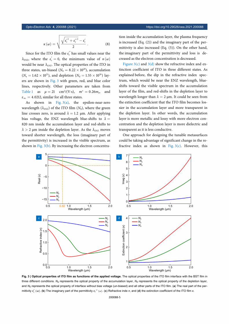
Since for the ITO film the has small values near the, where the , the minimum value of
would be near . The optical properties of the ITO inthree states, un-biased ( ), accumulation( ), and depletion ( ) lay-ers are shown in Fig. 3 with green, red, and blue colorlines, respectively. Other parameters are taken fromTable 1 as cm2/(V·s), , and
, similar for all three states.
λENZ N0
λ = 1.2λ =
820λ > 2 λENZ
As shown in Fig. 3(a), the epsilon-near-zerowavelength ( ) of the ITO film ( ), where the greenline crosses zero, is around μm. After applyingbias voltage, the ENZ wavelength blue-shifts to
nm inside the accumulation layer and red-shifts to μm inside the depletion layer. As the moves
toward shorter wavelength, the loss (imaginary part ofthe permittivity) is increased in the visible spectrum, asshown in Fig. 3(b). By increasing the electron concentra-
tion inside the accumulation layer, the plasma frequencyis increased (Eq. (2)) and the imaginary part of the per-mittivity is also increased (Eq. (5)). On the other hand,the imaginary part of the permittivity and loss is de-creased as the electron concentration is decreased.
λ = 2
Figure 3(c) and 3(d) show the refractive index and ex-tinction coefficient of ITO in three different states. Asexplained before, the dip in the refractive index spec-trum, which would be near the ENZ wavelength, blue-shifts toward the visible spectrum in the accumulationlayer of the film, and red-shifts in the depletion layer towavelength longer than μm. It could be seen fromthe extinction coefficient that the ITO film becomes los-sier in the accumulation layer and more transparent inthe depletion layer. In other words, the accumulationlayer is more metallic and lossy with more electron con-centration and the depletion layer is more dielectric andtransparent as it is less conductive.
One approach for designing the tunable metasurfacescould be taking advantage of significant change in the re-fractive index as shown in Fig. 3(c). However, this
5
0
−5
−10
−15
0.5 1.0Wavelength (μm)
1.5 2.0
Re
al (ϵ
)
0.82
7
6
5
4
3
2
1
0
Imag
(ϵ)
2.0
1.5
1.0
0.5
0.0
Refr
active in
de
x (n)
4
3
2
1
Extinction c
oeffic
ient
(κ)
0.5 1.0Wavelength (μm)
1.5 2.0
0.5 1.0Wavelength (μm)
1.5 2.0 0.5 1.0Wavelength (μm)
1.5 2.0
N0
Nd
N0
Nd
N0
Nd
N0
Nd
a b
c d
Na
Na Na
Na
ε′r (ω) εr′′ (ω)
Fig. 3 | Optical properties of ITO film as functions of the applied voltage. The optical properties of the ITO film interface with the BST film in
three different conditions. Na represents the optical property of the accumulation layer, Nd represents the optical property of the depletion layer,
and N0 represents the optical property of interface without bias voltage (un-biased) and all other parts of the ITO film. (a) The real part of the per-
mittivity . (b) The imaginary part of the permittivity . (c) Refractive inde n, and (d) the extinction coefficient of the ITO film κ.
Opto-Electron Adv 4, 200088 (2021) https://doi.org/10.29026/oea.2021.200088
200088-5
change only happens in very thin (~1 nm) accumulationand depletion layers. The better approach would be mak-ing use of the tunability of ENZ wavelength in the accu-mulation and depletion layers. The electric field wouldaccumulate and intensify inside the ENZ layer and resultin significant phase and intensity modulation34,35.However, these tunable metasurfaces suffer from low ef-ficiency due to the inherent high loss of accumulationlayer22,41, as shown in Fig. 3(b) and 3(d). In other words,the total efficiency of the metasurface is limited by theohmic loss of the ITO film. Here, this ohmic loss is go-ing to be used as an advantage to design a reflective mod-ulator using double ITO films. The modulator wouldhave two states of ON and OFF. In the ON state, the re-flection amplitude would be the maximum with ENZwavelength far away from the operational wavelength. Inthe OFF state, the reflection amplitude would decreasedramatically due to the high loss with ENZ shifting tothe operational wavelength.
D = 250W = 20
tITO = 5tBST = 50 tSi = 50
Figure 4 shows the unit cell of such electrically con-trolled modulator metasurface comprising a 100 nmthick silver mirror, circular-shaped ITO-BST-ITO reson-ator, and silicon resonator with nm diameter,and four nm wide bias connections on the sidesof resonators. The ITO, BST, and Si films are nm,
nm, and nm thick, respectively. All thetop ITO discs are connected through the top ITO film inbias connections. All the bottom ITO discs are electric-ally connected through the bottom Ag mirror and bot-tom ITO film in bias connections. A single voltagesource is used to control the charge accumulation anddepletion in the ITO discs, as shown in Fig. 4(b), and
tune the reflection amplitude of the light. Such a metas-urface could be fabricated by using ebeam lithography(EBL) and conventional semiconductor processing. Forexample, a 100 nm thick Ag film could be deposited us-ing ebeam evaporation on a highly doped Si substrate toallow the bottom ITO film to be addressed electricallythrough the substrate. Then the bottom ITO, BST, topITO, and Si films would be deposited using RF sputter-ing. The nano-disc structure could be created by EBLpatterning and plasma or deep reactive ion etching(DRIE) by using an appropriate masking layer. A post-annealing would be performed to increase the electronconcentration of ITO films.
dx× dy× dz = 5 nm×5 nm× 0.5 nm
N0 Na Nd
Due to the circular shape of the resonator and sym-metrical design of the bias connections on the four sidesof the resonator, the modulator metasurface is insensit-ive to the polarization of incident light, explained in de-tail in another work29. The performance of the modulat-or metasurface is simulated using Lumerical FDTD soft-ware. A single unit cell with periodic boundary condi-tions is simulated to numerically calculate the reflectionamplitude of the modulator metasurface. A local meshcell with dimensions of
is chosen for ITO discs to accuratelymodel the accumulation and depletion layers. The ITOfilm is modeled using the Drude model with the proper-ties measured and explored previously. The first 1 nmthick layer of the ITO films at the interface with BST filmis considered as the tunable accumulation/depletion lay-ers. The electron concentration of the first 0.5 nm nearBST film is changed from to or according to theapplied voltage, while the next 0.5 nm is changed
P
D
W V
X
Y
Z
V
Si
ITO
BST
Ag
a b
V
E
K
Fig. 4 | Schematic of the electrically controlled reflective modulator metasurface. (a) A square unit cell is constructed from a circular silicon
resonator on the top of a circular ITO-BST-ITO resonator on the top of a silver mirror. Four symmetrical bias connections with the same layers
are used to make bias connections between the ITO films. Parameter values are tAg =100 nm, tITO = 5 nm, tBST = 50 nm, tSi = 50 nm, W = 20 nm,
D = 250 nm, and P = 520 nm. The initial polarization of light is shown along the X axis. (b) 3D schematic of the metasurface constructed from a
6×6 array of unit cells. The metasurface is controlled by applying the voltage between the bottom silver film (grey) and the top ITO electrode (or-
ange). The electrical current passes to the resonators through a 2D array of bias connections.
Opto-Electron Adv 4, 200088 (2021) https://doi.org/10.29026/oea.2021.200088
200088-6

V = 0
N0 V = 2.5
Nd
Na
V = −2.5
Na Nd
according to the applied voltage and simulation results inFig. 2 to accurately model the accumulation (0.5 nm) anddepletion (1 nm) layers. Under V bias voltage(ON state), the electron concentration of both layers isconsidered . Under V bias voltage (OFF state1), the electron concentration of the top 0.5 nm tunablelayer is changed to (depletion layer) and the bottom0.5 nm tunable layer to (accumulation layer), whileunder V bias voltage (OFF state 2), the elec-tron concentration in the top 0.5 nm tunable layer ischanged to and the bottom 0.5 nm tunable layer to .
V = −2.5, 0 2.5
λ = 820
λ = 820 V = 0 56.3
V = −2.5
3.58× 10⁻³
V = 2.5
4.2
Simulated reflection spectra of the modulator underthree different voltages and V are shownin red, green, and blue colors, respectively, in Fig. 5(a).As explained before, the operational wavelength is set atthe ENZ wavelength of the accumulation layer, nm, to get the strongest resonance and thus the highestloss and the largest modulation depth. The reflectionamplitude at nm under V is %. It is adip in the reflection spectra mainly due to magnetic di-pole resonance in the ITO-BST-ITO resonator. By de-creasing the voltage to V (OFF state 2), the ac-cumulation layer is created at the bottom of the top ITOfilm which drops the reflection down to %.This is due to the coexistence of magnetic dipole reson-ance and ENZ wavelength inside the accumulation layerat this wavelength. If the voltage is reversed to V, the accumulation layer is created in the bottom ITOfilm and the reflection amplitude drops to % (OFFstate 1). As the distance between the accumulation layer
and the silver ground plane is changed, the resonancewavelength is slightly changed and the resonancestrength is slightly weakened. The modulation depth(MD) is defined as:
MD = 20log (RMax/RMin) , (9)
RMin = 3.58× 10⁻³ RMax = 56.3
λ = 820V = −2.5
V = −2.5
805 nm < λ < 835795 <
λ < 850 V = 2.5
790 <
λ < 860 785 < λ <
870
where % and % are theminimum and maximum reflection amplitudes before(ON state) and after (OFF state 2) applying the biasvoltage, respectively, at nm. Hence, under
V the proposed modulator metasurfaceachieves 84 dB modulation depth, equal to ~99.99%, ifdefined as MD = (|∆R|/RMax) × 100. Under V,where the accumulation layer is created in the top ITOfilm, the reflection amplitude remains below 1% (MD~40 dB) in the range of nm and re-mains below 5% (MD ~22 dB) in the range of nm
nm. Under V, where the accumulationlayer is created in the bottom ITO film, the reflectionamplitude remains below 1% in the range of nm
nm and below 5% in the range of nm nm.
V = 0
To investigate the phenomena behind such ultra-highmodulation depth, the electric field inside the resonatoris studied at the resonance wavelength (λ = 820 nm). Theelectric field intensity under three different bias voltagesis shown in Fig. 6. A field monitor is placed along the XZplane, according to Fig. 4, in the middle of the circularresonator. Under V bias voltage, it could be seenin Fig. 5 that there was a small dip in the reflection spec-trum at λ = 820 nm indicating a slight resonance in the
1.0
0.8
Reflection a
mp
litu
de (
a.u
.)
0.6
0.4
0.2
0.00.6 0.7 0.8 0.9
Wavelength (μm)1.0 1.1 1.2
V=0 VV=−2.5 VV=2.5 V
V=−2.5 V100
80
60
Mod
ula
tion d
epth
(d
B)
40
20
00.6 0.7 0.8 0.9
Wavelength (μm)1.0 1.1 1.2
λ=0.82
a b
Fig. 5 | Performance of the electrically tunable modulator metasurface. (a) Simulated reflection spectra of the modulator under three differ-
ent voltages. Under V = 0 V bias voltage, both ITO films have an electron concentration of N0. Under V = −2.5 V, the top ITO film has a 0.5 nm
thick accumulation layer with an electron concentration of Na and the bottom ITO film has a 1 nm thick depletion layer with an electron concentra-
tion of Nd. Under V = 2.5 V, the top ITO film has a depletion layer with an electron concentration of Nd and the bottom ITO film has an accumula-
tion layer with an electron concentration of Na. (b) Modulation depth spectra of modulator under V = −2.5 V. The modulation depth peaks to ~84
dB at the wavelength of λ = 820 nm.
Opto-Electron Adv 4, 200088 (2021) https://doi.org/10.29026/oea.2021.200088
200088-7

N0 = 8.22× 10²⁰
V = 2.5
resonator. The cause of that resonance could be seen inFig. 6(a), as the electric field is confined inside the topand bottom ITO discs. As explained earlier, ITO filmsare modeled using the Drude model with electron con-centration cm−3, implying semi-metal-lic properties of the ITO in visible and near-IR spectra.Moreover, the ENZ wavelength of un-biased ITO filmwas calculated in Table 1 as λENZ ~1.2 μm, relativelyclose to the wavelength of geometrical resonance, imply-ing a weak ENZ resonance inside the top and bottom cir-cular ITO discs. This geometrical resonance is a magnet-ic dipole resonance which would be explored in Fig. 7.By changing the voltage to V, the accumulationlayer is created in the bottom ITO layer interfacing theBST, as shown in Fig. 6(b). This accumulation layer hasthe ENZ wavelength at λ = 820 nm which was the reson-ance wavelength of the magnetic dipole resonator. Acombination of the electric field enhancement in theENZ layer and magnetic dipole resonance confines thelight inside the 0.5 nm thick ITO accumulation layer.This could also be explained as a narrow channel with adeep subwavelength transverse cross-section made ofENZ material, in the resonance wavelength42. As shownin Fig. 3(b) and 3(d), at the ENZ wavelength the accumu-lation layer becomes very lossy. This strong resonanceand confinement of the light inside a very thin accumu-lation layer cause total loss of the light with almost no re-flection, acting similar to a complete absorber. As shownin Fig. 5(a), due to the short distance between the ENZresonator and the ground plane, there are two identicalmagnetic dipole resonances around λ = 820 nm result-ing in two dips at λ = 795 nm and λ = 845 nm25.
V = −2.5As shown in Fig. 6(c), the same phenomenon happens
at V but the accumulation layer is created in-side the top ITO film interfacing with the BST disc. It isimportant to note that as the accumulation layer is cre-
λ > 2
ated inside one ITO disc, the depletion layer is created inthe other ITO disc. The depletion layer has a much lowerelectron concentration and its ENZ wavelength red-shifts to μm. This results in lower electric fieldconfinement compared to the un-biased ITO film andaccumulation layer, which could be seen in Fig. 6.
V = −2.5
To further investigate the resonance inside the accu-mulation layer, a field monitor is placed along the XYplane inside the accumulation layer in the top ITO filmunder a bias voltage of V. The electric andmagnetic fields at λ = 820 nm are shown in Fig. 7.
The electric and magnetic field intensities in the XYplane inside the accumulation layer are shown in Fig.7(a) and 7(b). The magnetic field looks like an ellipsestretched along the Y axis, while the electric field isstronger on the left and right side of the ENZ regionwhere the magnetic field is the weakest. This is in agree-ment with the polarization of light, where the electricfield was along the X axis and the magnetic field alongthe Y axis, as shown in Fig. 4(a). The top and side viewsof the electric field vectors are shown in Fig. 7(c) and7(e), respectively. The electric field vectors represent anelectric current in the shape of a stretched circular loop,antiparallel on two sides of the ENZ region. The top andside views of the magnetic field vectors are shown in Fig.7(d) and 7(f). The magnetic field vectors are stretchedalong the positive Y direction in the center of the ENZregion, strongest in the center of the ENZ region wherethe electric field is the weakest. All of this implies a mag-netic dipole stretched along the Y axis is created insidethe accumulation layer.
V = −2.5
Figure 8 shows the impact of the Si disc thickness onthe reflection spectra under the bias voltages of V = 0 Vand V. As shown in Fig. 8(a), under the biasvoltage of V = 0 V, the wavelength of the magnetic di-pole resonance is increasing from 630 nm to 820 nm as
300
275
250
225
200Z (
nm
)
175
150
125−200 −100 0
X (nm)100 200
Electric field intensity
80
70
60
50
40
30
20
10
0
300
275
250
225
200Z (
nm
)
175
150
125−200 −100 0
X (nm)100 200
300
275
250
225
200
Z (
nm
)
175
150
125−200 −100 0
X (nm)100 200
V=0 V V=2.5 V V=−2.5 V
Si
Ag Ag
Si
Ag
Si
a b c
Fig. 6 | Electric field intensity along XZ plane under the bias voltages of (a) V = 0 V at λ = 820 nm, (b) V = 2.5 V at λ = 800 nm, and (c) V = −2.5 V
at λ = 820 nm. The edges of the Si disc and silver mirror are shown with green dashed lines.
Opto-Electron Adv 4, 200088 (2021) https://doi.org/10.29026/oea.2021.200088
200088-8
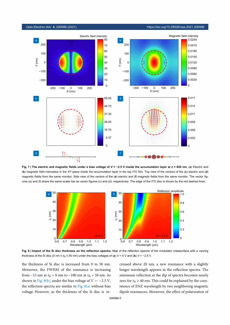
V = −2.5
the thickness of Si disc is increased from 0 to 50 nm.Moreover, the FWHM of the resonance is increasingfrom ~15 nm at tSi = 0 nm to ~100 nm at tSi = 50 nm. Asshown in Fig. 8(b), under the bias voltage of V,the reflection spectra are similar to Fig. 8(a) without biasvoltage. However, as the thickness of the Si disc is in-
creased above 20 nm, a new resonance with a slightlylonger wavelength appears in the reflection spectra. Theminimum reflection at the dip of spectra becomes nearlyzero for tSi ≥ 40 nm. This could be explained by the coex-istence of ENZ wavelength by two neighboring magneticdipole resonances. Moreover, the effect of polarization of
200
100
Y (
nm
)
0
−100
−200
−200 −100 0X (nm)
100 200
Electric field intensity
80
70
60
50
40
30
20
10
0
200
100
Y (
nm
)
0
−100
−200
−200 −100 0X (nm)
100 2000
0.0030
0.0060
0.0150
0.0120
0.0090
0.0180
0.0210
0.0240
56.00
46.70
37.30
28.00
18.70
9.37
0
0.017
0.014
0.011
0.009
0.006
0.003
0
a b
c d
e f
Magnetic field intensity
Fig. 7 | The electric and magnetic fields under a bias voltage of V = −2.5 V inside the accumulation layer at λ = 820 nm. (a) Electric and
(b) magnetic field intensities in the XY plane inside the accumulation layer in the top ITO film. Top view of the vectors of the (c) electric and (d)
magnetic fields from the same monitor. Side view of the vectors of the (e) electric and (f) magnetic fields from the same monitor. The vector fig-
ures (e) and (f) share the same scalar bar as vector figures (c) and (d), respectively. The edge of the ITO disc is shown by the red dashed lines.
50
40
30
t Si (
nm
)
20
10
00.6 0.7 0.8 0.9
Wavelength (μm)1.0 1.1 1.2
Reflection amplitude1.0
0.8
0.6
0.4
0.2
0V=0 V V=−2.5 V
0.6 0.7 0.8 0.9Wavelength (μm)
1.0 1.1 1.2
50
40
30
t Si (
nm
)
20
10
0
a b
Fig. 8 | Impact of the Si disc thickness on the reflection spectra. Map of the reflection spectra of the modulator metasurface with a varying
thickness of the Si disc (0 nm ≤ tSi ≤ 50 nm) under the bias voltages of (a) V = 0 V and (b) V = −2.5 V.
Opto-Electron Adv 4, 200088 (2021) https://doi.org/10.29026/oea.2021.200088
200088-9

incident light, angle of the incident light with the surfacenormal, the width of the bias connections, and ITO discsthickness are explored and the simulation results couldbe found in the Supplemental Material.
8.22× 1020 cm−3
The operational wavelength of the modulator is theresult of the coexistence of magnetic dipole resonanceand ENZ wavelength. Hence, both of them should beshifted to change the operational wavelength of the mod-ulator. The wavelength of magnetic dipole resonancecould be tuned by changing the diameter of the resonat-or. For example, by increasing the diameter of the circu-lar resonator, the wavelength of magnetic dipole reson-ance would increase. In such a case, the ENZ wavelengthof the accumulation layer inside the ITO film also shouldbe increased to this new longer wavelength. This couldbe achieved by either applying a smaller voltage betweenthe ITO films or choosing an ITO film with a lower ini-tial electron concentration (longer initial ENZwavelength). However, decreasing the operationalwavelength is not possible. The magnetic dipole reson-ance wavelength could be reduced by decreasing the dia-meter of the resonator. However, decreasing the ENZwavelength of the accumulation layer is not possiblesince it requires an increase in the initial electron concer-tation of the deposited ITO films which according to ourexperiments is maxed out at for 5 nmITO film. Note that increasing the applied voltage to fur-ther blue-shift the ENZ wavelength is not an answersince it may cause the breakdown of BST film due to ex-tremely high dielectric field.
Conclusion
λ = 820 nm805 < λ < 835
V = −2.5
An electrically tunable polarization-insensitive modulat-or metasurface operating in reflection mode was pro-posed. It has a tunable capacitive structure comprising ahigh dielectric constant perovskite BST film sandwichedbetween two ultra-thin 5 nm ITO films. These ITO filmsact as active tuning media through electron accumula-tion/depletion and also the electrodes for applying thebias voltage. The coupling of magnetic dipole resonancewith the ENZ wavelength inside the accumulation layerwas used to achieve the total absorption of reflected light.The metasurface achieved 84 dB or ~99.99% modulationdepth at the operation wavelength of and~40 dB in the wavelength range of nm nmunder V. By designing circular resonators andsymmetrical 2D bias connections, the metasurface wasinsensitive to the polarization of the incident light. The
proposed tunable metasurface could potentially be usedfor the active control of the light intensity with fast elec-trical signal modulation in the visible and near-IR spec-tra as a tunable flat optical interconnect, switch, andsensing device.
References Holloway CL, Kuester EF, Gordon JA, O'Hara J, Booth J et al.An overview of the theory and applications of metasurfaces:the two-dimensional equivalents of metamaterials. IEEEAntenn Propag Mag 54, 10–35 (2012).
1.
Yu NF, Capasso F. Flat optics with designer metasurfaces. NatMater 13, 139–150 (2014).
2.
Kildishev AV, Boltasseva A, Shalaev VM. Planar photonicswith metasurfaces. Science 339, 1232009 (2013).
3.
Zhang YB, Liu H, Cheng H, Tian JG, and Chen SQ. Multidi-mensional manipulation of wave fields based on artificial mi-crostructures. Opto-Electron Adv 3, 200002 (2020).
4.
Ni XJ, Kildishev AV, Shalaev VM. Metasurface holograms forvisible light. Nat Commun 4, 2807 (2013).
5.
Khorasaninejad M, Chen WT, Devlin RC, Oh J, Zhu AY et al.Metalenses at visible wavelengths: Diffraction-limited focusingand subwavelength resolution imaging. Science 352,1190–1194 (2016).
6.
Ma XL, Pu MB, Li X, Guo YH, Luo XG. All-metallic wide-anglemetasurfaces for multifunctional polarization manipulation.Opto-Electron Adv 2 , 180023 (2019).
7.
Glybovski SB, Tretyakov SA, Belov PA, Kivshar YS, SimovskiCR. Metasurfaces: from microwaves to visible. Phys Rep 634,1–72 (2016).
8.
Nemati A, Wang Q, Hong MH, Teng JH. Tunable and reconfig-urable metasurfaces and metadevices. Opto-Electron Adv 1,180009 (2018).
9.
Brar VW, Jang MS, Sherrott M, Lopez JJ, Atwater HA. Highlyconfined tunable mid-infrared plasmonics in graphene nanor-esonators. Nano Lett 13, 2541–2547 (2013).
10.
Sherrott MC, Hon PWC, Fountaine KT, Garcia JC, Ponti SM etal. Experimental demonstration of > 230° phase modulation ingate-tunable graphene–gold reconfigurable mid-infraredmetasurfaces. Nano Lett 17, 3027–3034 (2017).
11.
Ooi KJA, Leong PC, Ang LK, Tan DTH. All-optical control on agraphene-on-silicon waveguide modulator. Sci Rep 7, 12748(2017).
12.
Guo JY, Wang T, Quan BG, Zhao H, Gu CZ et al. Polarizationmultiplexing for double images display. Opto-Electron Adv 2 ,180029 (2019).
13.
Dou KH, Xie X, Pu MB, Li X, Ma XL et al. Off-axis multi-wavelength dispersion controlling metalens for multi-color ima-ging. Opto-Electron Adv 3 , 190005 (2020).
14.
Gao JW, Kempa K, Giersig M, Akinoglu EM, Han B et al. Phys-ics of transparent conductors. Adv Phys 65, 553–617 (2016).
15.
Chopra KL, Major S, Pandya DK. Transparent conductors—astatus review. Thin Solid Films 102, 1–46 (1983).
16.
Babicheva VE, Boltasseva A, Lavrinenko AV. Transparent con-ducting oxides for electro-optical plasmonic modulators. Nano-photonics 4, 165–185 (2015).
17.
Ou JY, Plum E, Zhang JF, Zheludev NI. An electromechanic-ally reconfigurable plasmonic metamaterial operating in the
18.
Opto-Electron Adv 4, 200088 (2021) https://doi.org/10.29026/oea.2021.200088
200088-10
near-infrared. Nat Nanotechnol 8, 252–255 (2013). Ee HS, Agarwal R. Tunable metasurface and flat optical zoomlens on a stretchable substrate. Nano Lett 16, 2818–2823(2016).
19.
Liu L, Kang L, Mayer TS, Werner DH. Hybrid metamaterials forelectrically triggered multifunctional control. Nat Commun 7,13236 (2016).
20.
ForouzmA, Salary MM, Inampudi S, Mosallaei H. A tunablemultigate Indium‐Tin‐oxide‐assisted all‐dielectric metas-urface. Adv Opt Mater 6, 1701275 (2018).
21.
Kafaie Shirmanesh G, Sokhoyan R, Pala RA, Atwater HA.Dual-gated active metasurface at 1550 nm with wide (> 300°)phase tunability. Nano Lett 18, 2957–2963 (2018).
22.
Huang YW, Lee HW, Sokhoyan R, Pala RA, Thyagarajan K etal. Gate-tunable conducting oxide metasurfaces. Nano Lett 16,5319–5325 (2016).
23.
Park J, Jeong BG, Kim SI, Lee D, Kim J et al. All-solid-statespatial light modulator with independent phase and amplitudecontrol for three-dimensional LiDAR applications. Nat Nano-technol 16, 69–76 (2021).
24.
Park J, Kang JH, Liu XG, Brongersma ML. Electrically tunableepsilon-near-zero (ENZ) metafilm absorbers. Sci Rep 5, 15754(2015).
25.
Shi KF, Haque RR, Zhao BY, Zhao RC, Lu ZL. Broadbandelectro-optical modulator based on transparent conducting ox-ide. Opt Lett 39, 4978–4981 (2014).
26.
Lee Y, Yun J, Kim SJ, Seo M, In S et al. High‐speed trans-mission control in gate‐ tunable metasurfaces using hybridplasmonic waveguide mode. Adv Opt Mater 8, 2001256(2020).
27.
Howes A, Wang WY, Kravchenko I, Valentine J. Dynamictransmission control based on all-dielectric Huygens metasur-faces. Optica 5, 787–792 (2018).
28.
Nemati A, Qian W, Hong MH, Teng JH. Electrically tunable po-larization-insensitive MIM plasmonic metasurface operating intransmission mode. J Opt 21, 055102 (2019).
29.
Edwards PP, Porch A, Jones MO, Morgan DV, Perks RM. Ba-sic materials physics of transparent conducting oxides. DaltonTrans 19, 2995–3002 (2004).
30.
Alù A, Silveirinha MG, Salandrino A, Engheta N. Epsilon-near-zero metamaterials and electromagnetic sources: Tailoring theradiation phase pattern. Phys Rev B 75, 155410 (2007).
31.
Liberal I, Engheta N. The rise of near-zero-index technologies.Science 358, 1540–1541 (2017).
32.
Naik GV, Kim J, Boltasseva A. Oxides and nitrides as alternat-ive plasmonic materials in the optical range[Invited]. Opt Mater
33.
Express 1, 1090–1099 (2011). Kinsey N, DeVault C, Boltasseva A, Shalaev VM. Near-zero-in-dex materials for photonics. Nat Rev Mater 4, 742–760 (2019).
34.
Lobet M, Liberal I, Knall EN, Alam MZ, Reshef O et al. Funda-mental radiative processes in near-zero-index media of vari-ous dimensionalities. ACS Photonics 7, 1965–1970 (2020).
35.
Chen AQ, Zhu KG, Zhong HC, Shao QY, Ge GL. A new invest-igation of oxygen flow influence on ITO thin films by magnet-ron sputtering. Solar Energy Mater Solar Cells 120, 157–162(2014).
36.
Izumi H, Adurodija FO, Kaneyoshi T, Ishihara T, Yoshioka H etal. Electrical and structural properties of indium tin oxide filmsprepared by pulsed laser deposition. J Appl Phys 91,1213–1218 (2002).
37.
Gorzkowski EP, Pan MJ, Bender B, Wu CCM. Glass-ceramicsof barium strontium titanate for high energy density capacitors.J Electroceram 18, 269–276 (2007).
38.
Vidhya VS, Malathy V, Balasubramanian T, Saaminathan V,Sanjeeviraja C et al. Influence of RF power on the growthmechanism, preferential orientation and optoelectronic proper-ties of nanocrystalline ITO films. Curr Appl Phys 11, 286–294(2011).
39.
Fan JCC, Goodenough JB. X‐ ray photoemission spectro-scopy studies of Sn‐doped indium‐oxide films. J Appl Phys48, 3524–3531 (1977).
40.
Forouzmand A, Salary MM, Shirmanesh GK, Sokhoyan R, At-water HA et al. Tunable all-dielectric metasurface for phasemodulation of the reflected and transmitted light via permittivitytuning of indium tin oxide. Nanophotonics 8, 415–427 (2019).
41.
Silveirinha MG, Engheta N. Theory of supercoupling, squeez-ing wave energy, and field confinement in narrow channelsand tight bends using ε near-zero metamaterials. Phys Rev B76, 245109 (2007).
42.
AcknowledgementsThis work is supported by the Agency for Science, Technology and Re-search (A*STAR) under AME IRG Grant No. A2083c0058, AME IAF-PPGrant No. 182 24 30030, HBMS IAF-PP Grant No. H19H6a0025, and byMOE Tier 3 program LUNI170919aPUBMOE.
Competing interestsThe authors declare no competing financial interests.
Supplementary informationSupplementary information for this paper is available athttps://doi.org/10.29026/oea.2021.200088
Opto-Electron Adv 4, 200088 (2021) https://doi.org/10.29026/oea.2021.200088
200088-11