ucc2871x constant-voltage, constant-current … · vdd vs ucc28710 cbc gnd hv drv cs +! vout vac...
TRANSCRIPT

VDD
VS
UCC28710
CBC
GND
HV
DRV
CS
+
–
VOUT
VAC
VAUX
UDG-12200
Product
Folder
Order
Now
Technical
Documents
Tools &
Software
Support &Community
ReferenceDesign
An IMPORTANT NOTICE at the end of this data sheet addresses availability, warranty, changes, use in safety-critical applications,intellectual property matters and other important disclaimers. PRODUCTION DATA.
UCC28710, UCC28711, UCC28712, UCC28713SLUSB86C –NOVEMBER 2012–REVISED JUNE 2017
UCC2871x Constant-Voltage, Constant-Current Controller With Primary-Side Regulation
1
1 Features1• < 10-mW No-Load Power• Primary-Side Regulation (PSR) Eliminates Opto-
Coupler• ±5% Voltage and Current Regulation Across Line
and Load• 700-V Start-Up Switch• 100-kHz Maximum Switching Frequency Enables
High-Power Density Charger Designs• Resonant Valley-Switching Operation for Highest
Overall Efficiency• Frequency Jitter to Ease EMI Compliance• Wide VDD Range Allows Small Bias Capacitor• Clamped Gate-Drive Output for MOSFET• Overvoltage, Low-Line, and Overcurrent
Protection Functions• Programmable Cable Compensation (UCC28710)• NTC Resistor Interface (UCC28711, UCC28712
and UCC28713) with Fixed Cable CompensationOptions
• SOIC-7 Package• Create a Custom Design Using the UCC28710
With the WEBENCH® Power Designer
2 Applications• USB-Compliant Adapters and Chargers for
Consumer Electronics– Smart Phones– Tablet Computers– Cameras
• Standby Supply for TV and Desktop• White Goods
3 DescriptionThe UCC2871x family of flyback power supplycontrollers provides isolated-output Constant-Voltage(CV) and Constant-Current (CC) output regulationwithout the use of an optical coupler. The devicesprocess information from the primary power switchand an auxiliary flyback winding for precise control ofoutput voltage and current.
An internal 700-V start-up switch, dynamically-controlled operating states and a tailored modulationprofile support ultra-low standby power withoutsacrificing start-up time or output transient response.
Control algorithms in the UCC28710 family allowoperating efficiencies to meet or exceed applicablestandards. The output drive interfaces to a MOSFETpower switch. Discontinuous conduction mode (DCM)with valley switching reduces switching losses.Modulation of switching frequency and primarycurrent peak amplitude (FM and AM) keeps theconversion efficiency high across the entire load andline ranges.
The controllers have a maximum switching frequencyof 100 kHz and always maintain control of the peak-primary current in the transformer. Protection featureshelp keep primary and secondary componentstresses in check. The UCC28710 allow the cablecompensation to be programmed. The UCC28711,UCC28712 and UCC28713 devices allow remotetemperature sensing using a negative temperaturecoefficient (NTC) resistor while providing fixed cable-compensation levels.
Device Information(1)
PART NUMBER PACKAGE BODY SIZE (NOM)UCC28710
SOIC (7) 4.91 mm × 3.90 mmUCC28711UCC28712UCC28713
(1) For all available packages, see the orderable addendum atthe end of the data sheet.
Simplified Application

2
UCC28710, UCC28711, UCC28712, UCC28713SLUSB86C –NOVEMBER 2012–REVISED JUNE 2017 www.ti.com
Product Folder Links: UCC28710 UCC28711 UCC28712 UCC28713
Submit Documentation Feedback Copyright © 2012–2017, Texas Instruments Incorporated
Table of Contents1 Features .................................................................. 12 Applications ........................................................... 13 Description ............................................................. 14 Revision History..................................................... 25 Device Comparison Table ..................................... 36 Pin Configuration and Functions ......................... 37 Specifications......................................................... 4
7.1 Absolute Maximum Ratings ...................................... 47.2 ESD Ratings.............................................................. 47.3 Recommended Operating Conditions....................... 47.4 Thermal Information .................................................. 47.5 Electrical Characteristics........................................... 57.6 Typical Characteristics .............................................. 6
8 Detailed Description .............................................. 98.1 Overview ................................................................... 98.2 Functional Block Diagram ......................................... 98.3 Feature Description................................................. 10
8.4 Device Functional Modes........................................ 129 Application and Implementation ........................ 17
9.1 Application Information............................................ 179.2 Typical Application .................................................. 17
10 Power Supply Recommendations ..................... 2311 Layout................................................................... 23
11.1 Layout Guidelines ................................................. 2311.2 Layout Example .................................................... 25
12 Device and Documentation Support ................. 2612.1 Device Support...................................................... 2612.2 Documentation Support ........................................ 2812.3 Receiving Notification of Documentation Updates 2812.4 Community Resources.......................................... 2812.5 Trademarks ........................................................... 2812.6 Electrostatic Discharge Caution............................ 2912.7 Glossary ................................................................ 29
13 Mechanical, Packaging, and OrderableInformation ........................................................... 29
4 Revision HistoryNOTE: Page numbers for previous revisions may differ from page numbers in the current version.
Changes from Revision B (July 2015) to Revision C Page
• Deleted all references to the UCC28714, UCC28715, and UCC28716 devices.................................................................... 1• Deleted quasi from quasi-resonant......................................................................................................................................... 1• Added the Development Support, Receiving Notification of Documentation Updates, and Community Resources
sections................................................................................................................................................................................. 26
Changes from Revision A (December 2014) to Revision B Page
• Updated Layout Guidelines section...................................................................................................................................... 23
Changes from Original (November 2012) to Revision A Page
• Added Pin Configuration and Functions section, ESD Ratings table, Feature Description section, Device FunctionalModes, Application and Implementation section, Power Supply Recommendations section, Layout section, Deviceand Documentation Support section, and Mechanical, Packaging, and Orderable Information section .............................. 1

VDD
VS
NTC
GND
HV
DRV
CS
1
2
3
4
7
6
5
VDD
VS
CBC
GND
HV
DRV
CS
1
2
3
4
7
6
5
3
UCC28710, UCC28711, UCC28712, UCC28713www.ti.com SLUSB86C –NOVEMBER 2012–REVISED JUNE 2017
Product Folder Links: UCC28710 UCC28711 UCC28712 UCC28713
Submit Documentation FeedbackCopyright © 2012–2017, Texas Instruments Incorporated
(1) See Mechanical, Packaging, and Orderable Information section for specific device ordering information.(2) For other fixed cable compensation options, call TI.
5 Device Comparison Table
PART NUMBER (1) MINIMUM SWITCHINGFREQUENCY OPTIONS (2)
UCC28710
680 Hz
Programmable cable compensationUCC28711 NTC option, 0-mV (at 5-V output) cable compensationUCC28712 NTC option, 150-mV (at 5-V output) cable compensationUCC28713 NTC option, 300-mV (at 5-V output) cable compensation
6 Pin Configuration and Functions
UCC28710 D Package7-Pin SOICTop View
UCC28711, UCC28712, UCC28713 D Package7-Pin SOICTop View
Pin FunctionsPIN
I/O DESCRIPTIONNAME UCC28710
UCC28711UCC28712UCC28713
CBC 3 — I Cable compensation is a programming pin for compensation of cable voltage drop. Cablecompensation is programmed with a resistor to GND.
CS 5 5 I
Current sense input connects to a ground-referenced current-sense resistor in series withthe power switch. The resulting voltage is used to monitor and control the peak primarycurrent. A series resistor can be added to this pin to compensate the peak switch currentlevels as the AC-mains input varies.
DRV 6 6 O Drive is an output used to drive the gate of an external high voltage MOSFET switchingtransistor.
GND 4 4 —The ground pin is both the reference pin for the controller and the low-side return for thedrive output. Special care should be taken to return all AC decoupling capacitors as closeas possible to this pin and avoid any common trace length with analog signal return paths.
HV 7 7 I The high-voltage pin connects directly to the rectified bulk voltage and provides charge tothe VDD capacitor for start-up of the power supply.
NTC — 3 I NTC an interface to an external negative temperature coefficient resistor for remotetemperature sensing. Pulling this pin low shuts down PWM action.
VDD 1 1 I VDD is the bias supply input pin to the controller. A carefully-placed bypass capacitor toGND is required on this pin.
VS 2 2 I
Voltage sense is an input used to provide voltage and timing feedback to the controller.This pin is connected to a voltage divider between an auxiliary winding and GND. Thevalue of the upper resistor of this divider is used to program the AC-mains run and stopthresholds and line compensation at the CS pin.

4
UCC28710, UCC28711, UCC28712, UCC28713SLUSB86C –NOVEMBER 2012–REVISED JUNE 2017 www.ti.com
Product Folder Links: UCC28710 UCC28711 UCC28712 UCC28713
Submit Documentation Feedback Copyright © 2012–2017, Texas Instruments Incorporated
(1) Stresses beyond those listed under Absolute Maximum Ratings may cause permanent damage to the device. These are stress ratingsonly and functional operation of the device at these or any other conditions beyond those indicated under Recommended OperatingConditions is not implied. Exposure to absolute-maximum-rated conditions for extended periods may affect device reliability. All voltagesare with respect to GND. Currents are positive into, negative out of the specified terminal. These ratings apply over the operatingambient temperature ranges unless otherwise noted.
7 Specifications
7.1 Absolute Maximum RatingsSee (1).
MIN MAX UNITVHV Start-up pin voltage, HV 700 VVVDD Bias supply voltage, VDD 38 VIDRV Continuous gate current sink 50 mAIDRV Continuous gate current source Self-limiting mAIVS Peak current, VS −1.2 mAVDRV Gate drive voltage at DRV −0.5 Self-limiting V
VoltageVS −0.75 7 VCS, CBC, NTC −0.5 5 V
TJ Operating junction temperature −55 150 °CLead temperature 0.6 mm from case for 10 s 260 °C
Tstg Storage temperature −65 150 °C
(1) JEDEC document JEP155 states that 500-V HBM allows safe manufacturing with a standard ESD control process.(2) JEDEC document JEP157 states that 250-V CDM allows safe manufacturing with a standard ESD control process. .
7.2 ESD RatingsVALUE UNIT
V(ESD)Electrostaticdischarge
Human-body model (HBM), per ANSI/ESDA/JEDEC JS-001 (1) ±2000V
Charged-device model (CDM), per JEDEC specification JESD22-C101 (2) ±500
7.3 Recommended Operating Conditionsover operating free-air temperature range (unless otherwise noted)
MIN NOM MAX UNITVDD Bias supply operating voltage 9 35 VCVDD VDD bypass capacitor 0.047 1 µFRCBC Cable-compensation resistance 10 kΩIVS VS pin current −1 mATJ Operating junction temperature −40 125 °C
(1) For more information about traditional and new thermal metrics, see the Semiconductor and IC Package Thermal Metrics applicationreport.
7.4 Thermal Information
THERMAL METRIC (1)UCC2871x
UNITD (SOIC)7 PINS
RθJA Junction-to-ambient thermal resistance 141.5 °C/WRθJC(top) Junction-to-case (top) thermal resistance 73.8 °C/WRθJB Junction-to-board thermal resistance 89 °C/WψJT Junction-to-top characterization parameter 23.5 °C/WψJB Junction-to-board characterization parameter 88.2 °C/W
5
UCC28710, UCC28711, UCC28712, UCC28713www.ti.com SLUSB86C –NOVEMBER 2012–REVISED JUNE 2017
Product Folder Links: UCC28710 UCC28711 UCC28712 UCC28713
Submit Documentation FeedbackCopyright © 2012–2017, Texas Instruments Incorporated
(1) The regulating level at VS decreases with temperature by 0.8 mV/˚C. This compensation is included to reduce the power supply outputvoltage variance over temperature.
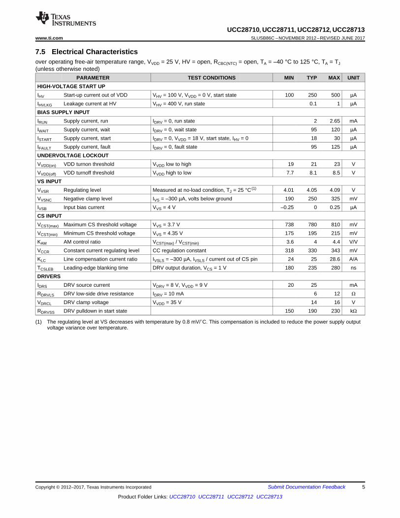
7.5 Electrical Characteristicsover operating free-air temperature range, VVDD = 25 V, HV = open, RCBC(NTC) = open, TA = –40 °C to 125 °C, TA = TJ(unless otherwise noted)
PARAMETER TEST CONDITIONS MIN TYP MAX UNITHIGH-VOLTAGE START UPIHV Start-up current out of VDD VHV = 100 V, VVDD = 0 V, start state 100 250 500 µAIHVLKG Leakage current at HV VHV = 400 V, run state 0.1 1 µABIAS SUPPLY INPUTIRUN Supply current, run IDRV = 0, run state 2 2.65 mAIWAIT Supply current, wait IDRV = 0, wait state 95 120 µAISTART Supply current, start IDRV = 0, VVDD = 18 V, start state, IHV = 0 18 30 µAIFAULT Supply current, fault IDRV = 0, fault state 95 125 µAUNDERVOLTAGE LOCKOUTVVDD(on) VDD turnon threshold VVDD low to high 19 21 23 VVVDD(off) VDD turnoff threshold VVDD high to low 7.7 8.1 8.5 VVS INPUTVVSR Regulating level Measured at no-load condition, TJ = 25 °C (1) 4.01 4.05 4.09 VVVSNC Negative clamp level IVS = –300 µA, volts below ground 190 250 325 mVIVSB Input bias current VVS = 4 V –0.25 0 0.25 µACS INPUTVCST(max) Maximum CS threshold voltage VVS = 3.7 V 738 780 810 mVVCST(min) Minimum CS threshold voltage VVS = 4.35 V 175 195 215 mVKAM AM control ratio VCST(max) / VCST(min) 3.6 4 4.4 V/VVCCR Constant current regulating level CC regulation constant 318 330 343 mVKLC Line compensation current ratio IVSLS = –300 µA, IVSLS / current out of CS pin 24 25 28.6 A/ATCSLEB Leading-edge blanking time DRV output duration, VCS = 1 V 180 235 280 nsDRIVERSIDRS DRV source current VDRV = 8 V, VVDD = 9 V 20 25 mARDRVLS DRV low-side drive resistance IDRV = 10 mA 6 12 Ω
VDRCL DRV clamp voltage VVDD = 35 V 14 16 VRDRVSS DRV pulldown in start state 150 190 230 kΩ

0.0001
0.001
0.01
0.1
1
10
0 5 10 15 20 25 30 35
I VD
D -
Bia
s S
uppl
y C
urre
nt (
mA
)
VDD - Bias Supply Voltage (V) C001
Run State
VDD Turn-Off
Wait State
VDD Turn-On
Start State
/\ \/
0.0001
0.001
0.01
0.1
1
10
-50 -25 0 25 50 75 100 125
I VD
D -
Bia
s S
uppl
y C
urre
nt (
mA
)
TJ - Temperature (oC) C002
IRUN, VDD = 25V
IWAIT, VDD = 25V
ISTART, VDD = 18V
6
UCC28710, UCC28711, UCC28712, UCC28713SLUSB86C –NOVEMBER 2012–REVISED JUNE 2017 www.ti.com
Product Folder Links: UCC28710 UCC28711 UCC28712 UCC28713
Submit Documentation Feedback Copyright © 2012–2017, Texas Instruments Incorporated
Electrical Characteristics (continued)over operating free-air temperature range, VVDD = 25 V, HV = open, RCBC(NTC) = open, TA = –40 °C to 125 °C, TA = TJ(unless otherwise noted)
PARAMETER TEST CONDITIONS MIN TYP MAX UNITTIMINGfSW(max) Maximum switching frequency VVS = 3.7 V 92 100 106 kHz
fSW(min) Minimum switching frequency VVS = 4.35 V
UCC28710UCC28711UCC28712UCC28713
600 680 755 Hz
tZTO Zero-crossing timeout delay 1.8 2.1 2.55 µsPROTECTIONVOVP Overvoltage threshold At VS input, TJ = 25 °C (1) 4.55 4.6 4.71 VVOCP Overcurrent threshold At CS input 1.4 1.5 1.6 VIVSL(run) VS line-sense run current Current out of VS pin increasing 190 225 275 µAIVSL(stop) VS line-sense stop current Current out of VS pin decreasing 70 80 100 µAKVSL VS line sense ratio IVSL(run) / IVSL(stop) 2.45 2.8 3.05 A/ATJ(stop) Thermal shut-down temperature Internal junction temperature 165 °CCABLE COMPENSATION
VCBC(max)Cable compensation maximumvoltage Voltage at CBC at full load UCC28710 2.9 3.2 3.5 V
VCVS(min) Compensation at VS VCBC = open, change in VSregulating level at full load UCC28710 –55 –15 25 mV
VCVS(max) Maximum compensation at VS VCBC = 0 V, change in VS regulatinglevel at full load UCC28710 275 320 375 mV
VCVS Compensation at VS Change in VS regulating level at fullload
UCC28711 –55 –15 25mVUCC28712 103
UCC28713 206NTC INPUT
VNTCTH NTC shut-down threshold Fault UVLO cycle when below thisthreshold
UCC28711UCC28712UCC28713
0.9 0.95 1 V
INTC NTC pullup current Current out of pinUCC28711UCC28712UCC28713
90 105 125 µA
7.6 Typical CharacteristicsVDD = 25 V, unless otherwise noted.
Figure 1. Bias Supply Current vs. Bias Supply Voltage Figure 2. Bias Supply Current vs. Temperature

550
575
600
625
650
675
700
725
750
775
-50 -25 0 25 50 75 100 125
f SW
(min
) - M
inim
um S
witc
hing
Fre
quen
cy (
Hz)
TJ - Temperature (oC) C007
20
22
24
26
28
30
32
34
-50 -25 0 25 50 75 100 125
I DR
S -
DR
V S
ourc
e C
urre
nt (
mA
)
TJ - Temperature (oC) C008
VDRV = 8 V, VVDD = 9 V
170
175
180
185
190
195
200
205
210
-50 -25 0 25 50 75 100 125
VC
ST
(min
) - M
inim
um C
S T
hres
hold
Vol
tage
(m
V)
TJ - Temperature (oC) C005
310
315
320
325
330
335
340
345
350
-50 -25 0 25 50 75 100 125
VC
CR -
Con
stan
t C
urre
nt R
egul
atin
g Le
vel (
mV
)
TJ - Temperature (oC) C006
3.94
3.96
3.98
4
4.02
4.04
4.06
4.08
4.1
4.12
-50 -25 0 25 50 75 100 125
VV
SR -
VS
Reg
ulat
ion
Vol
tage
(V
)
TJ - Temperature (oC) C003
0
50
100
150
200
250
300
-50 -25 0 25 50 75 100 125
VS
Lin
e S
ense
Cur
rent
(�
A)
TJ - Temperature (oC) C004
IVSLRUN
IVSLSTOP
7
UCC28710, UCC28711, UCC28712, UCC28713www.ti.com SLUSB86C –NOVEMBER 2012–REVISED JUNE 2017
Product Folder Links: UCC28710 UCC28711 UCC28712 UCC28713
Submit Documentation FeedbackCopyright © 2012–2017, Texas Instruments Incorporated
Typical Characteristics (continued)VDD = 25 V, unless otherwise noted.
Figure 3. VS Regulation Voltage vs. Temperature Figure 4. VS Line Sense Current vs. Temperature
Figure 5. Minimum CS Threshold vs. Temperature Figure 6. Constant Current Regulating Level vs.Temperature
Figure 7. Minimum Switching Frequency vs. Temperature
VDRV = 8 V VVDD = 9 V
Figure 8. DRV Source Current vs. Temperature

4.52
4.54
4.56
4.58
4.60
4.62
4.64
4.66
4.68
-50 -25 0 25 50 75 100 125
VO
VP -
VS
Ove
r-V
olta
ge T
hres
hold
(V
)
TJ - Temperature (oC) C011
0
40
80
120
160
200
240
280
320
-50 -25 0 25 50 75 100 125
I HV -
HV
Sta
rt-U
p C
urre
nt (�
A)
TJ - Temperature (oC) C012
0.90
0.92
0.94
0.96
0.98
1.00
-50 -25 0 25 50 75 100 125
VN
TC
TH -
NT
C S
hutd
own
Thr
esho
ld V
olta
ge (
V)
TJ - Temperature (oC) C009
90
95
100
105
110
115
120
-50 -25 0 25 50 75 100 125
I NT
C -
NT
C P
ull-U
p C
urre
nt (�
A)
TJ - Temperature (oC) C010
8
UCC28710, UCC28711, UCC28712, UCC28713SLUSB86C –NOVEMBER 2012–REVISED JUNE 2017 www.ti.com
Product Folder Links: UCC28710 UCC28711 UCC28712 UCC28713
Submit Documentation Feedback Copyright © 2012–2017, Texas Instruments Incorporated
Typical Characteristics (continued)VDD = 25 V, unless otherwise noted.
Figure 9. NTC Shutdown Threshold Voltage vs. Temperature Figure 10. NTC Pull-Up Current vs. Temperature
Figure 11. VS Overvoltage Threshold vs. Temperature Figure 12. HV Start-Up Current vs. Temperature
DRV
25 mA
S Q
QR
CS+
VS SAMPLER
+E/A
4.05 V + VCVS
CBC
VDD
POWER
& FAULT
MANAGEMENT
UVLO
21 V / 8 V
VALLEY
SWITCHING
CONTROL
LAW
LEB
1 / fSWVCST
SECONDARY
TIMING
DETECT
CURRENT
REGULATION VCST
200 kΩ
VDD
LINE
SENSE
+
ICBC
0 V-VCVS(max)
GND
CABLE
COMPENSATION
VCVS = ICBC x 3 kΩ
+
VOVPOV FAULT
OV FAULTTSD/SD FAULT
IVSLS
+10 kΩ LINE
FAULT
LINE FAULT
14 V
2.2 V / 0.80 V
+ VNTCTH
NTC
INTC
TSD/SD
FAULT
UCC28710/14/15 UCC28711/12/13
+
1.5 VOC FAULT
OC FAULT
IVSLS / KLCIVSLS
28 kΩ
5 V
5 V
HV
IHV
9
UCC28710, UCC28711, UCC28712, UCC28713www.ti.com SLUSB86C –NOVEMBER 2012–REVISED JUNE 2017
Product Folder Links: UCC28710 UCC28711 UCC28712 UCC28713
Submit Documentation FeedbackCopyright © 2012–2017, Texas Instruments Incorporated
8 Detailed Description
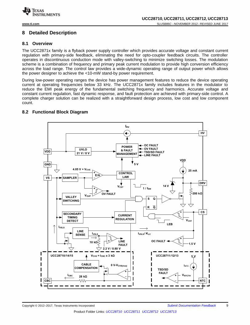
8.1 OverviewThe UCC2871x family is a flyback power supply controller which provides accurate voltage and constant currentregulation with primary-side feedback, eliminating the need for opto-coupler feedback circuits. The controlleroperates in discontinuous conduction mode with valley-switching to minimize switching losses. The modulationscheme is a combination of frequency and primary peak current modulation to provide high conversion efficiencyacross the load range. The control law provides a wide-dynamic operating range of output power which allowsthe power designer to achieve the <10-mW stand-by power requirement.
During low-power operating ranges the device has power management features to reduce the device operatingcurrent at operating frequencies below 33 kHz. The UCC2871x family includes features in the modulator toreduce the EMI peak energy of the fundamental switching frequency and harmonics. Accurate voltage andconstant current regulation, fast dynamic response, and fault protection are achieved with primary-side control. Acomplete charger solution can be realized with a straightforward design process, low cost and low componentcount.
8.2 Functional Block Diagram

( )S1 VSR
S2
AS OCV F VSR
R VR
N V V V
´=
´ + -
IN(run)S1
PA VSL(run)
V 2R
N I
´
=
´
10
UCC28710, UCC28711, UCC28712, UCC28713SLUSB86C –NOVEMBER 2012–REVISED JUNE 2017 www.ti.com
Product Folder Links: UCC28710 UCC28711 UCC28712 UCC28713
Submit Documentation Feedback Copyright © 2012–2017, Texas Instruments Incorporated
8.3 Feature Description
8.3.1 Detailed Pin Description
8.3.1.1 VDD (Device Bias Voltage Supply)The VDD pin is connected to a bypass capacitor to ground and a start-up resistance to the input bulk capacitor(+) terminal. The VDD turnon UVLO threshold is 21 V and turnoff UVLO threshold is 8.1 V, with an availableoperating range up to 35 V. The USB charging specification requires the output current to operate in constant-current mode from 5 V to a minimum of 2 V; this is easily achieved with a nominal VDD of approximately 25 V.The additional VDD headroom up to 35 V allows for VDD to rise due to the leakage energy delivered to the VDDcapacitor in high-load conditions. Also, the wide VDD range provides the advantage of selecting a relatively smallVDD capacitor and high-value start-up resistance to minimize no-load stand-by power loss in the start-upresistor.
8.3.1.2 GND (Ground)This is a single ground reference external to the device for the gate drive current and analog signal reference.Place the VDD bypass capacitor close to GND and VDD with short traces to minimize noise on the VS and CSsignal pins.
8.3.1.3 VS (Voltage-Sense)The VS pin is connected to a resistor divider from the auxiliary winding to ground. The output-voltage feedbackinformation is sampled at the end of the transformer secondary current demagnetization time to provide anaccurate representation of the output voltage. Timing information to achieve valley-switching and to control theduty cycle of the secondary transformer current is determined by the waveform on the VS pin. Avoid placing afilter capacitor on this input which would interfere with accurate sensing of this waveform.
The VS pin also senses the bulk capacitor voltage to provide for AC-input run and stop thresholds, and tocompensate the current-sense threshold across the AC-input range. This information is sensed during theMOSFET on-time. For the AC-input run/stop function, the run threshold on VS is 220 µA and the stop thresholdis 80 µA. The values for the auxilliary voltage divider upper-resistor RS1 and lower-resistor RS2 can bedetermined by the equations below.
where• NPA is the transformer primary-to-auxiliary turns ratio,• VIN(run) is the AC RMS voltage to enable turnon of the controller (run),• IVSL(run) is the run-threshold for the current pulled out of the VS pin during the MOSFET on-time. (see the
Electrical Characteristics table) (1)
where• VOCV is the converter regulated output voltage,• VF is the output rectifier forward drop at near-zero current,• NAS is the transformer auxiliary to secondary turns ratio,• RS1 is the VS divider high-side resistance,• VVSR is the CV regulating level at the VS input (see the Electrical Characteristics table). (2)

( )CBC(max) OCV FCBC
VSR OCBC
V 3 k V VR 28 k
V V
´ W ´ += - W
´
LC S1 CS D PALC
P
K R R T NR
L
´ ´ ´ ´
=
CCR PSCS XFMR
OCC
V NR
2I
´= ´ h
11
UCC28710, UCC28711, UCC28712, UCC28713www.ti.com SLUSB86C –NOVEMBER 2012–REVISED JUNE 2017
Product Folder Links: UCC28710 UCC28711 UCC28712 UCC28713
Submit Documentation FeedbackCopyright © 2012–2017, Texas Instruments Incorporated
Feature Description (continued)8.3.1.4 DRV (Gate Drive)The DRV pin is connected to the MOSFET gate pin, usually through a series resistor. The gate driver provides agate-drive signal limited to 14 V. The turnon characteristic of the driver is a 25-mA current source which limits theturnon dv/dt of the MOSFET drain and reduces the leading-edge current spike, but still provides gate-drivecurrent to overcome the Miller plateau. The gate-drive turnoff current is determined by the low-side driver RDS(on)and any external gate-drive resistance. The user can reduce the turnoff MOSFET drain dv/dt by adding externalgate resistance.
8.3.1.5 CS (Current Sense)The current-sense pin is connected through a series resistor (RLC) to the current-sense resistor (RCS). Thecurrent-sense threshold is 0.75 V for IPP(max) and 0.25 V for IPP(min). The series resistor RLC provides the functionof feed-forward line compensation to eliminate change in IPP due to change in di/dt and the propagation delay ofthe internal comparator and MOSFET turnoff time. There is an internal leading-edge blanking time of 235 ns toeliminate sensitivity to the MOSFET turnon current spike. It should not be necessary to place a bypass capacitoron the CS pin. The value of RCS is determined by the target output current in constant-current (CC) regulation.The values of RCS and RLC can be determined by the equations below. The term ηXFMR is intended to account forthe energy stored in the transformer but not delivered to the secondary. This includes transformer resistance andcore loss, bias power, and primary-to-secondary leakage ratio.
Example: With a transformer core and winding loss of 5%, primary-to-secondary leakage inductance of 3.5%,and bias power to output power ratio of 1.5%. The ηXFMR value is approximately: 1 - 0.05 - 0.035 - 0.015 = 0.9.
where• VCCR is a current regulation constant (see the Electrical Characteristics table),• NPS is the transformer primary-to-secondary turns ratio (a ratio of 13 to 15 is recommended for 5-V output),• IOCC is the target output current in constant-current regulation,• ηXFMR is the transformer efficiency. (3)
where• RS1 is the VS pin high-side resistor value,• RCS is the current-sense resistor value,• TD is the current-sense delay including MOSFET turnoff delay, add ~50 ns to MOSFET delay,• NPA is the transformer primary-to-auxiliary turns ratio,• LP is the transformer primary inductance,• KLC is a current-scaling constant (see the Electrical Characteristics table). (4)
8.3.1.6 CBC (Cable Compensation), Pin 1 UCC28700The cable compensation pin is connected to a resistor to ground to program the amount of output voltagecompensation to offset cable resistance. The cable compensation block provides a 0-V to 3-V voltage level onthe CBC pin corresponding to 0 to IOCC output current. The resistance selected on the CBC pin programs acurrent mirror that is summed into the VS feedback divider therefore increasing the output voltage as IOUTincreases. There is an internal series resistance of 28 kΩ to the CBC pin which sets a maximum cablecompensation of a 5-V output to 400 mV when CBC is shorted to ground. The CBC resistance value can bedetermined by the equation below.
12
UCC28710, UCC28711, UCC28712, UCC28713SLUSB86C –NOVEMBER 2012–REVISED JUNE 2017 www.ti.com
Product Folder Links: UCC28710 UCC28711 UCC28712 UCC28713
Submit Documentation Feedback Copyright © 2012–2017, Texas Instruments Incorporated
Feature Description (continued)where
• VO is the output voltage,• VF is the diode forward voltage,• VOCBC is the target cable compensation voltage at the output terminals,• VCBC(max) is the maximum voltage at the cable compensation pin at the maximum converter output current (see
the Electrical Characteristics table),• VVSR is the CV regulating level at the VS input (see the Electrical Characteristics table). (5)
8.3.1.7 NTC (NTC Thermistor Shut-down), Pin 1 UCC28701/2/3These versions of the UCC28700 family utilize pin 1 for an external NTC thermistor to allow user-programmableexternal thermal shut-down. The shut-down threshold is 0.95 V with an internal 105-µA current source whichresults in a 9.05-kΩ thermistor shut-down threshold. These controllers have either zero or fixed internal cablecompensation.
8.3.2 Fault ProtectionThere is comprehensive fault protection. Protection functions include:• Output overvoltage fault• Input undervoltage fault• Internal overtemperature fault• Primary overcurrent fault• CS pin fault• VS pin fault
A UVLO reset and restart sequence applies for all fault protection events.
The output overvoltage function is determined by the voltage feedback on the VS pin. If the voltage sample onVS exceeds 115% of the nominal VOUT, the device stops switching and the internal current consumption is IFAULTwhich discharges the VDD capacitor to the UVLO turnoff threshold. After that, the device returns to the start stateand a start-up sequence ensues.
The UCC2871x family always operates with cycle-by-cycle primary peak current control. The normal operatingrange of the CS pin is 0.78 V to 0.195 V. There is additional protection if the CS pin reaches 1.5 V. This resultsin a UVLO reset and restart sequence.
The line input run and stop thresholds are determined by current information at the VS pin during the MOSFETon-time. While the VS pin is clamped close to GND during the MOSFET on-time, the current through RS1 ismonitored to determine a sample of the bulk capacitor voltage. A wide separation of run and stop thresholdsallows clean start-up and shut-down of the power supply with the line voltage. The run current threshold is 225µA and the stop current threshold is 80 µA.
The internal over-temperature protection threshold is 165°C. If the junction temperature reaches this thresholdthe device initiates a UVLO reset cycle. If the temperature is still high at the end of the UVLO cycle, theprotection cycle repeats.
Protection is included in the event of component failures on the VS pin. If complete loss of feedback informationon the VS pin occurs, the controller stops switching and restarts.
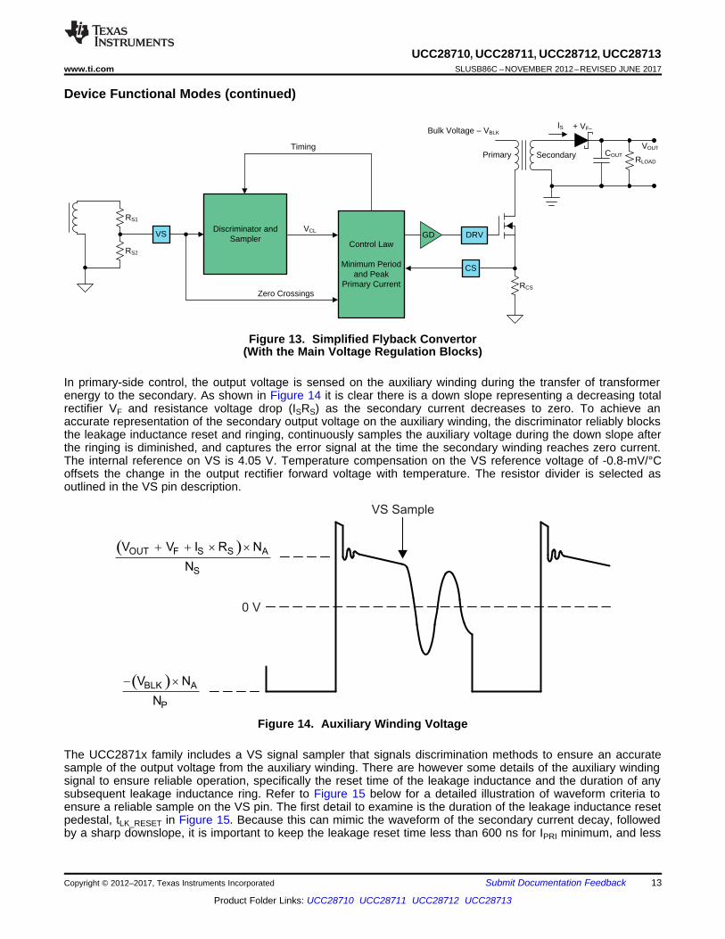
8.4 Device Functional Modes
8.4.1 Primary-Side Voltage RegulationFigure 13 illustrates a simplified flyback convertor with the main voltage regulation blocks of the device shown.The power train operation is the same as any DCM flyback circuit but accurate output voltage and currentsensing is the key to primary-side control.
VS Sample
0 V
( )OUT F S S A
S
V V I R N
N
+ + ´ ´
( )BLK A
P
V N
N
- ´
RS1
RS2
VSDiscriminator and
SamplerControl Law
Minimum Period and Peak
Primary Current
VCL
Timing
Zero Crossings
DRV
CS
RCS
RLOADCOUT
VOUT
ISBulk Voltage ± VBLK
Primary Secondary
+ VF±
GD
13
UCC28710, UCC28711, UCC28712, UCC28713www.ti.com SLUSB86C –NOVEMBER 2012–REVISED JUNE 2017
Product Folder Links: UCC28710 UCC28711 UCC28712 UCC28713
Submit Documentation FeedbackCopyright © 2012–2017, Texas Instruments Incorporated
Device Functional Modes (continued)
Figure 13. Simplified Flyback Convertor(With the Main Voltage Regulation Blocks)
In primary-side control, the output voltage is sensed on the auxiliary winding during the transfer of transformerenergy to the secondary. As shown in Figure 14 it is clear there is a down slope representing a decreasing totalrectifier VF and resistance voltage drop (ISRS) as the secondary current decreases to zero. To achieve anaccurate representation of the secondary output voltage on the auxiliary winding, the discriminator reliably blocksthe leakage inductance reset and ringing, continuously samples the auxiliary voltage during the down slope afterthe ringing is diminished, and captures the error signal at the time the secondary winding reaches zero current.The internal reference on VS is 4.05 V. Temperature compensation on the VS reference voltage of -0.8-mV/°Coffsets the change in the output rectifier forward voltage with temperature. The resistor divider is selected asoutlined in the VS pin description.
Figure 14. Auxiliary Winding Voltage
The UCC2871x family includes a VS signal sampler that signals discrimination methods to ensure an accuratesample of the output voltage from the auxiliary winding. There are however some details of the auxiliary windingsignal to ensure reliable operation, specifically the reset time of the leakage inductance and the duration of anysubsequent leakage inductance ring. Refer to Figure 15 below for a detailed illustration of waveform criteria toensure a reliable sample on the VS pin. The first detail to examine is the duration of the leakage inductance resetpedestal, tLK_RESET in Figure 15. Because this can mimic the waveform of the secondary current decay, followedby a sharp downslope, it is important to keep the leakage reset time less than 600 ns for IPRI minimum, and less

Control Voltage, E/A Output - VCL
Control Law Profile in Constant Voltage (CV) Mode
f SW
(1/
MIN
P)
I PP
(pe
ak
pri
ma
rycu
rre
nt)
5 V3.55 V2.2 V1.3 V0.75 V
IPP(max)100 kHz
fSW(min)
fSW
IPP
IPP(max) / 4.033 kHz
3.3 kHz
AMFM FM
VS Ring (p-p)
tLK_RESET
tDM
tSMPL
UDG-12202
14
UCC28710, UCC28711, UCC28712, UCC28713SLUSB86C –NOVEMBER 2012–REVISED JUNE 2017 www.ti.com
Product Folder Links: UCC28710 UCC28711 UCC28712 UCC28713
Submit Documentation Feedback Copyright © 2012–2017, Texas Instruments Incorporated
Device Functional Modes (continued)than 2.2 µs for IPRI maximum. The second detail is the amplitude of ringing on the VAUX waveform followingtLK_RESET. The peak-to-peak voltage at the VS pin should be less than approximately 100 mVp-p at least 200 nsbefore the end of the demagnetization time, tDM. If there is a concern with excessive ringing, it usually occursduring light or no-load conditions, when tDM is at the minimum. The tolerable ripple on VS is scaled up to theauxiliary winding voltage by RS1 and RS2, and is equal to 100 mV x (RS1 + RS2) / RS2.
Figure 15. Auxiliary Waveform Details
During voltage regulation, the controller operates in frequency modulation mode and amplitude modulation modeas illustrated in Figure 16 below. The internal operating frequency limits of the device are 100 kHz maximum andfSW(min). The transformer primary inductance and primary peak current chosen sets the maximum operatingfrequency of the converter. The output preload resistor and efficiency at low power determines the converterminimum operating frequency. There is no stability compensation required for the UCC2871x family.
Figure 16. Frequency and Amplitude Modulation Modes(During Voltage Regulation)

VOCV
IOCC
Outp
ut V
oltage (
V)
UDG-12201
Output Current
1
2
3
4
5
4.75 V
5.25 V
±5%
PP P DMOUT
S SW
I N tI
2 N t= ´ ´
IPP
UDG-12203
tON
tDM
tSW
NP
IS S
N´
15
UCC28710, UCC28711, UCC28712, UCC28713www.ti.com SLUSB86C –NOVEMBER 2012–REVISED JUNE 2017
Product Folder Links: UCC28710 UCC28711 UCC28712 UCC28713
Submit Documentation FeedbackCopyright © 2012–2017, Texas Instruments Incorporated
Device Functional Modes (continued)8.4.2 Primary-Side Current RegulationTiming information at the VS pin and current information at the CS pin allow accurate regulation of the secondaryaverage current. The control law dictates that as power is increased in CV regulation and approaching CCregulation the primary-peak current is at IPP(max). Referring to Figure 17 below, the primary-peak current, turnsratio, secondary demagnetization time (tDM), and switching period (tSW) determine the secondary average outputcurrent. Ignoring leakage inductance effects, the average output current is given by Equation 6. When theaverage output current reaches the regulation reference in the current control block, the controller operates infrequency modulation mode to control the output current at any output voltage at or below the voltage regulationtarget as long as the auxiliary winding can keep VDD above the UVLO turnoff threshold.
Figure 17. Transformer Currents
(6)
Figure 18. Typical Target Output V-I Characteristic
8.4.3 Valley SwitchingThe UCC2871x family utilizes valley switching to reduce switching losses in the MOSFET, to reduce induced-EMI, and to minimize the turnon current spike at the sense resistor. The controller operates in valley-switching inall load conditions unless the VDS ringing has diminished.

VDRV
VDS
16
UCC28710, UCC28711, UCC28712, UCC28713SLUSB86C –NOVEMBER 2012–REVISED JUNE 2017 www.ti.com
Product Folder Links: UCC28710 UCC28711 UCC28712 UCC28713
Submit Documentation Feedback Copyright © 2012–2017, Texas Instruments Incorporated
Device Functional Modes (continued)Referring to Figure 19 below, the UCC2871x family operates in a valley-skipping mode in most load conditions tomaintain an accurate voltage or current regulation point and still switch on the lowest available VDS voltage.
Figure 19. Valley-Skipping Mode
8.4.4 Start-Up OperationThe internal high-voltage start-up switch connected to the bulk capacitor voltage (VBLK) through the HV pincharges the VDD capacitor. During start up there is typically 300 µA available to charge the VDD capacitor.When VDD reaches the 21-V UVLO turnon threshold, the controller is enabled, the converter starts switching andthe start-up switch is turned off. The initial three cycles are limited to IPP(min). After the initial three cycles atminimum IPP(min), the controller responds to the condition dictated by the control law. The converter will remain indiscontinuous mode during charging of the output capacitor(s), maintaining a constant output current until theoutput voltage is in regulation.

+ VFA -
RCS
+
–
DRV
CS
CDD
VDD
GND
RS1
RS2
VS
COUTVOUT
CB2 Np Ns
Na
VAUX
RPL
VAC
CBC
HV
UCC28710
SOIC-7
RLC
+ VF -VBLK
CB1
RCBC
17
UCC28710, UCC28711, UCC28712, UCC28713www.ti.com SLUSB86C –NOVEMBER 2012–REVISED JUNE 2017
Product Folder Links: UCC28710 UCC28711 UCC28712 UCC28713
Submit Documentation FeedbackCopyright © 2012–2017, Texas Instruments Incorporated
9 Application and Implementation
NOTEInformation in the following applications sections is not part of the TI componentspecification, and TI does not warrant its accuracy or completeness. TI’s customers areresponsible for determining suitability of components for their purposes. Customers shouldvalidate and test their design implementation to confirm system functionality.
9.1 Application InformationThe UCC2871x family of flyback power supply controllers provides constant voltage (CV) and constant current(CC) output regulation to help meet USB-compliant adaptors and charger requirements. These devices use theinformation obtained from auxiliary winding sensing (VS) to control the output voltage and do not requireoptocoupler/TL431 feedback circuitry. Eliminating the optocoupler feedback reduces component count andmakes the design more cost effective. Refer to Figure 20 for details.
9.2 Typical ApplicationThe procedure in the Detailed Design Procedure section outlines the steps to design a constant-voltage,constant-current flyback converter using the UCC2871x family of controllers. Refer to the typical applicationschematic for component location (Figure 20) and the Device Nomenclature section for variable definitions.
Figure 20. Design Procedure Application Example
9.2.1 Design Requirements
Table 1. Design ParametersPARAMETER NOTES AND CONDITIONS MIN NOM MAX UNIT
INPUT CHARACTERISTICSVIN Input Voltage 100 115/230 240 VfLINE Line Frequency 47 50/60 64 HzPSB_CONV No Load Input Power VIN = Nom, IO = 0 A 10 mWVIN(RUN) Brownout Voltage IO = Nom 70 VOUTPUT CHARACTERISTICSVO Output Voltage VIN = Nom, IO = Nom 4.75 5 5.25 VVRIPPLE Output Voltage Ripple VIN = Nom, IO = Max 0.1 VIO Output Current VIN = Min to Max 1 1.05 A

SB SB _ CONVP P 2.5 mW= +
2OCV
PLSB _ CONV
VR
P 2.5 mW=
-
OUT MINSB _ CONV 2
SB AM MAX
P fP
K f
´=
h ´ ´
18
UCC28710, UCC28711, UCC28712, UCC28713SLUSB86C –NOVEMBER 2012–REVISED JUNE 2017 www.ti.com
Product Folder Links: UCC28710 UCC28711 UCC28712 UCC28713
Submit Documentation Feedback Copyright © 2012–2017, Texas Instruments Incorporated
Typical Application (continued)Table 1. Design Parameters (continued)
PARAMETER NOTES AND CONDITIONS MIN NOM MAX UNITVOVP Output OVP IOUT = Min to Max 5.75 V
Transient Response
VOΔ Load Step (VO = 4.1 V to 6 V)(0.1 to 0.6 A) or (0.6 to 0.1 A)VOΔ = 0.9 V for COUT calculationin applications section
4.1 5 6 A
SYSTEMS CHARACTERISTICSSwitching Frequency 90 kHz
η Full Load Efficiency (115/230 V RMSInput) IO = 1 A 74% 76%
9.2.2 Detailed Design Procedure
9.2.2.1 Custom Design With WEBENCH® ToolsClick here to create a custom design using the UCC28710 device with the WEBENCH® Power Designer.1. Start by entering the input voltage (VIN), output voltage (VOUT), and output current (IOUT) requirements.2. Optimize the design for key parameters such as efficiency, footprint, and cost using the optimizer dial.3. Compare the generated design with other possible solutions from Texas Instruments.
The WEBENCH Power Designer provides a customized schematic along with a list of materials with real-timepricing and component availability.
In most cases, these actions are available:• Run electrical simulations to see important waveforms and circuit performance• Run thermal simulations to understand board thermal performance• Export customized schematic and layout into popular CAD formats• Print PDF reports for the design, and share the design with colleagues
Get more information about WEBENCH tools at www.ti.com/WEBENCH.
9.2.2.2 Stand-by Power EstimateAssuming no-load stand-by power is a critical design parameter, determine estimated no-load power based ontarget converter maximum switching frequency and output power rating.
The following equation estimates the stand-by power of the converter.
(7)
For a typical USB charger application, the bias power during no-load is approximately 2.5 mW. This is based on25-V VDD and 100-µA bias current. The output preload resistor can be estimated by VOCV and the difference inthe converter stand-by power and the bias power. The equation for output preload resistance accounts for biaspower estimated at 2.5 mW.
(8)
The capacitor bulk voltage for the loss estimation is the highest voltage for the stand-by power measurement,typically 325 VDC.
For the total stand-by power estimation add an estimated 2.5 mW for snubber loss to the converter stand-bypower loss.
(9)

CCR PSCS XFMR
OCC
V NR
2I
´= ´ h
( )MAX BULK(min)
PS(max)MAGCC OCV F OCBC
D VN
D V V V
´=
´ + +
RMAX MAX MAGCC
tD 1 f D
2
æ ö= - ´ -ç ÷
è ø
( )
BULK(min)IN
IN(min)
BULK 2 2IN(min) BULK(min) LINE
V12P 0.25 arcsin
2 2 VC
2V V f
æ öæ öç ÷ç ÷´ + ´
ç ÷ç P ÷´è øè ø=- ´
OCV OCCIN
V IP
´=
h
19
UCC28710, UCC28711, UCC28712, UCC28713www.ti.com SLUSB86C –NOVEMBER 2012–REVISED JUNE 2017
Product Folder Links: UCC28710 UCC28711 UCC28712 UCC28713
Submit Documentation FeedbackCopyright © 2012–2017, Texas Instruments Incorporated
9.2.2.3 Input Bulk Capacitance and Minimum Bulk VoltageDetermine the minimum voltage on the input capacitance, CB1 and CB2 total, in order to determine the maximumNp to Ns turns ratio of the transformer. The input power of the converter based on target full-load efficiency,minimum input RMS voltage, and minimum AC input frequency are used to determine the input capacitancerequirement.
Maximum input power is determined based on VOCV, IOCC, and the full-load efficiency target.
(10)
The below equation provides an accurate solution for input capacitance based on a target minimum bulkcapacitor voltage. To target a given input capacitance value, iterate the minimum capacitor voltage to achieve thetarget capacitance.
(11)
9.2.2.4 Transformer Turns Ratio, Inductance, Primary-Peak CurrentThe maximum primary-to-secondary turns ratio can be determined by the target maximum switching frequency atfull load, the minimum input capacitor bulk voltage, and the estimated DCM resonant time.
Initially determine the maximum available total duty cycle of the on time and secondary conduction time based ontarget switching frequency and DCM resonant time. For DCM resonant time, assume 500 kHz if you do not havean estimate from previous designs. For the transition mode operation limit, the period required from the end ofsecondary current conduction to the first valley of the VDS voltage is ½ of the DCM resonant period, or 1 µsassuming 500-kHz resonant frequency. DMAX can be determined using the equation below.
(12)
Once DMAX is known, the maximum turns ratio of the primary to secondary can be determined with the equationbelow. DMAGCC is defined as the secondary diode conduction duty cycle during constant-current, CC, operation. Itis set internally by the UCC2871x family at 0.425. The total voltage on the secondary winding needs to bedetermined; which is the sum of VOCV, the secondary rectifier VF, and the cable compensation voltage (VOCBC).For the 5-V USB charger applications, a turns ratio range of 13 to 15 is typically used.
(13)
Once an optimum turns ratio is determined from a detailed transformer design, use this ratio for the followingparameters.
The UCC2871x family constant-current regulation is achieved by maintaining a maximum DMAG duty cycle of0.425 at the maximum primary current setting. The transformer turns ratio and constant-current regulatingvoltage determine the current sense resistor for a target constant current.
Since not all of the energy stored in the transformer is transferred to the secondary, a transformer efficiency termis included. This efficiency number includes the core and winding losses, leakage inductance ratio, and biaspower ratio to rated output power. For a 5-V, 1-A charger example, bias power of 1.5% is a good estimate. Anoverall transformer efficiency of 0.9 is a good estimate to include 3.5% leakage inductance, 5% core and windingloss, and 1.5% bias power.
(14)
The primary transformer inductance can be calculated using the standard energy storage equation for flybacktransformers. Primary current, maximum switching frequency and output and transformer power losses areincluded in the equation below. Initially determine transformer primary current.
Primary current is simply the maximum current sense threshold divided by the current sense resistance.

RIPPLEESR
PP(max) PS
V 0.8R
I N
´
=
´
TRANSW(min)
OUTO
1I 150 s
fC
V D
æ ö+ mç ÷ç ÷
è ø=
( )( )
( )
ON IN max
DMAG minPS OCV F
t V 2
tN V V
´ ´=
´ +
( )( )
( ) ( )
( )
PP max CST minP
ON min
CST maxIN max
I VLt
VV 2
´= ´
´
� � � �DSPK IN(max) OCV F OCBC PS LKV V 2 V V V N V u � � � u �
IN(max)REV OCV OCBC
PS
V 2V V V
N
´
= + +
DD(off ) FAAS
OCC F
V VN
V V
+
=
+
( )OCV F OCBC OCCP 2
XFMR PP(max) MAX
2 V V V IL
I f
+ + ´=
h ´ ´
CST(max)PP(max)
CS
VI
R=
20
UCC28710, UCC28711, UCC28712, UCC28713SLUSB86C –NOVEMBER 2012–REVISED JUNE 2017 www.ti.com
Product Folder Links: UCC28710 UCC28711 UCC28712 UCC28713
Submit Documentation Feedback Copyright © 2012–2017, Texas Instruments Incorporated
(15)
(16)
The secondary winding to auxiliary winding transformer turns ratio (NAS) is determined by the lowest targetoperating output voltage in constant-current regulation and the VDD UVLO of the UCC2871x family. There isadditional energy supplied to VDD from the transformer leakage inductance energy which allows a lower turnsratio to be used in many designs.
(17)
9.2.2.5 Transformer Parameter VerificationThe transformer turns ratio selected affects the MOSFET VDS and secondary rectifier reverse voltage so theseshould be reviewed. The UCC2871x family does require a minimum on time of the MOSFET (tON) and minimumDMAG time (tDMAG) of the secondary rectifier in the high line, minimum load condition. The selection of fMAX, LPand RCS affects the minimum tON and tDMAG.
The secondary rectifier and MOSFET voltage stress can be determined by the equations below.
(18)
For the MOSFET VDS voltage stress, an estimated leakage inductance voltage spike (VLK) needs to be included.
(19)
Equation 20 and Equation 21 are used to determine if the minimum tON target of 300 ns and minimum tDMAGtarget of 1.2 µs is achieved.
(20)
(21)
9.2.2.6 Output CapacitanceThe output capacitance value is typically determined by the transient response requirement from no-load. Forexample, in some USB charger applications there is a requirement to maintain a minimum VO of 4.1 V with aload-step transient of 0 mA to 500 mA . The equation below assumes that the switching frequency can be at theUCC2871x family's minimum of fSW(min).
(22)
Another consideration of the output capacitor(s) is the ripple voltage requirement which is reviewed based onsecondary peak current and ESR. A margin of 20% is added to the capacitor ESR requirement in the equationbelow.
(23)

Output Power
Effi
cien
cy
10% 20% 30% 40% 50% 60% 70% 80% 90% 100%64%
66%
68%
70%
72%
74%
76%
78%
D001
Efficiency at 115 VRMSEfficiency at 230 VRMS
( )CBC(max) OCV FCBC
VSR OCBC
V 3 k V VR 28 k
V V
´ W ´ += - W
´
LC S1 CS D PALC
P
K R R t NR
L
´ ´ ´ ´
=
( )S1 VSR
S2
AS OCV F VSR
R VR
N V V V
´=
´ + -
IN(run)S1
PA VSL(run)
V 2R
N I
´
=
´
( )
( )
OUT OCCRUN
OCCDD
DD(on) DD(off )
C VI 1mA
IC
V V 1 V
´+ ´
=- -
21
UCC28710, UCC28711, UCC28712, UCC28713www.ti.com SLUSB86C –NOVEMBER 2012–REVISED JUNE 2017
Product Folder Links: UCC28710 UCC28711 UCC28712 UCC28713
Submit Documentation FeedbackCopyright © 2012–2017, Texas Instruments Incorporated
9.2.2.7 VDD Capacitance, CDD
The capacitance on VDD needs to supply the device operating current until the output of the converter reachesthe target minimum operating voltage in constant-current regulation. At this time the auxiliary winding can sustainthe voltage to the UCC2871x family. The total output current available to the load and to charge the outputcapacitors is the constant-current regulation target. The equation below assumes the output current of theflyback is available to charge the output capacitance until the minimum output voltage is achieved. There is anestimated 1 mA of gate-drive current in the equation and 1 V of margin added to VDD.
(24)
9.2.2.8 VS Resistor Divider, Line Compensation, and Cable CompensationThe VS divider resistors determine the output voltage regulation point of the flyback converter, also the high-sidedivider resistor (RS1) determines the line voltage at which the controller enables continuous DRV operation. RS1is initially determined based on transformer auxiliary to primary turns ratio and desired input voltage operatingthreshold.
(25)
The low-side VS pin resistor is selected based on desired VO regulation voltage.
(26)
The UCC2871x family can maintain tight constant-current regulation over input line by utilizing the linecompensation feature. The line compensation resistor (RLC) value is determined by current flowing in RS1 andexpected gate drive and MOSFET turnoff delay. Assume a 50-ns internal delay in the UCC2871x family.
(27)
On the UCC28710, which has adjustable cable compensation, the resistance for the desired compensation levelat the output terminals can be determined using Equation 28.
(28)
9.2.3 Application Curves
Figure 21. Efficiency Figure 22. Output at Startup at 115-V RMS(No Load)

22
UCC28710, UCC28711, UCC28712, UCC28713SLUSB86C –NOVEMBER 2012–REVISED JUNE 2017 www.ti.com
Product Folder Links: UCC28710 UCC28711 UCC28712 UCC28713
Submit Documentation Feedback Copyright © 2012–2017, Texas Instruments Incorporated
Figure 23. Output at Startup at 115-V RMS(5-Ω Load)
Figure 24. Output at Startup at 230-V RMS(No Load)
Figure 25. Output at Startup at 230-V RMS(5-Ω Load)
CH1 = IO, CH4 = VO With a 5-V Offset
Figure 26. Load Transients:(0.1-A to 0.6-A Load Step)
CH1 = IO, CH4 = VO With a 5-V Offset
Figure 27. Load Transients:(0.6-A to 0.1-A Load Step)
CH4 = VO, Output voltage at EVM outputCH2 = VO, Output voltage measured at the end of the 3M ofcable in parallel with a 1-uF capacitor. The output voltage hasless than 50 mV of output ripple at the end of the cable.
Figure 28. Output Ripple Voltage at Full Load

23
UCC28710, UCC28711, UCC28712, UCC28713www.ti.com SLUSB86C –NOVEMBER 2012–REVISED JUNE 2017
Product Folder Links: UCC28710 UCC28711 UCC28712 UCC28713
Submit Documentation FeedbackCopyright © 2012–2017, Texas Instruments Incorporated
10 Power Supply RecommendationsThe UCC2871x family is intended for AC/DC adapters and chargers with input voltage range of 85 VAC(rms) to 265VAC(rms) using Flyback topology. It can be used in other applications and converter topologies with different inputvoltages. Be sure that all voltages and currents are within the recommended operating conditions and absolutemaximum ratings of the device. To maintain output current regulation over the entire input voltage range, designthe converter to operate close to fMAX when in full-load conditions. To improve thermal performance increase thecopper area connected to GND pins.
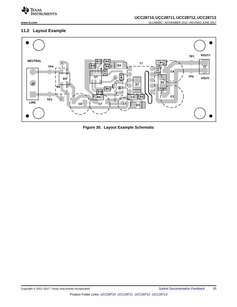
11 Layout
11.1 Layout Guidelines• High frequency bypass Capacitor C5 should be placed across Pin 1 and 4 as close as you can get it to the
pins.• Resistor R4 and C5 form a low pass filter and the connection of R4 and C5 should be as close to the VDD
pin as possible.• The VS pin controls the output voltage through the transformer turns ratio and the voltage divider of R5 and
R11. Note the trace length between the R5, R11 and VS pin should be as short as possible to reduce oreliminate possible EMI coupling.
• Note the IC ground and power ground should meet at the bulk capacitor’s (C6 and C7) return. Try to ensurethat high frequency/high current from the power stage does not go through the signal ground.– The high frequency/high current path that you need to be cautious of on the primary is C7 +, T1 (P5, P3),
Q1d, Q1s, R8 to the return of C6 and C7. Try to keep all high current loops as short as possible.• Try to keep all high current loops as short as possible.• Keep all high current/high frequency traces away from or perpendicular to other traces in the design.• Traces on the voltage clamp formed by D1, R2, D3 and C2 as short as possible.• C6 return needs to be as close to the bulk capacitor supply as possible. This reduces the magnitude of dv/dt
caused by large di/dt.• Avoid mounting semiconductors under magnetics.
Line
Neutral
VOUT +
VOUT -
VIN = 90V to 256V RMS
Vout = 5V/1A+ C3
560 uF
3
2
1
J2
+ C4
560 uF
+ C6
4.7 uF
+ C7
4.7 uF
J1
D2
B340LB-13-F
R710.0k
R610
R81.96
R1127.4k
R582.5k
R10
100k R121.00kC5
330nF
D4
RS1B-13-F
TP3
TP4
TP1
TP2
R4
22.5
D3
SMBJP6KE82A
C2
1nF
R2
649
R315.4k
D5
HD06
Q1
STD2HNK70Z-1
3
4
51
2
7
9
T17508110127REV01
1 VDD
2 VS
3 CBC/NTC
4 GND
5CS
6DRV
8HV
U1
UCC28711D
L1
470 uH
D1
MURS160-13-F
C1
1nF
R1
39
R9
10 ohm Fusible Resistor
1 2
JP1
Copyright © 2017, Texas Instruments Incorporated
UCC28710, UCC28711, UCC28712, UCC28713SLUSB86C –NOVEMBER 2012–REVISED JUNE 2017 www.ti.com
24
Product Folder Links: UCC28710 UCC28711 UCC28712 UCC28713
Submit Documentation Feedback Copyright © 2012–2017, Texas Instruments Incorporated
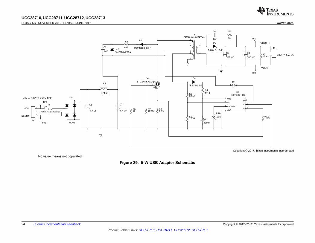
No value means not populated.
Figure 29. 5-W USB Adapter Schematic
U1
1
D5
TP3
TP4
J2
LINE
NEUTRAL
VOUT+
VOUT-
TP1
TP2
R9
C6 C7
C4
C3
J1R10
R11 R5
R4
C5
D4
R12
R6
R7
Q1
JP
1 D1
T1
L1
R2C2
D3
C1
R1
D2
R8
25
UCC28710, UCC28711, UCC28712, UCC28713www.ti.com SLUSB86C –NOVEMBER 2012–REVISED JUNE 2017
Product Folder Links: UCC28710 UCC28711 UCC28712 UCC28713
Submit Documentation FeedbackCopyright © 2012–2017, Texas Instruments Incorporated
11.2 Layout Example
Figure 30. Layout Example Schematic

26
UCC28710, UCC28711, UCC28712, UCC28713SLUSB86C –NOVEMBER 2012–REVISED JUNE 2017 www.ti.com
Product Folder Links: UCC28710 UCC28711 UCC28712 UCC28713
Submit Documentation Feedback Copyright © 2012–2017, Texas Instruments Incorporated
12 Device and Documentation Support
12.1 Device Support
12.1.1 Development SupportFor design tools see the UCC2871x Calculator, UCC2871x PSpice Transient Model, UCC2871x TINA-TITransient Spice Model, and UCC2871x TINA-TI Transient Reference Design.
12.1.1.1 Custom Design With WEBENCH® ToolsClick here to create a custom design using the UCC28710 device with the WEBENCH® Power Designer.1. Start by entering the input voltage (VIN), output voltage (VOUT), and output current (IOUT) requirements.2. Optimize the design for key parameters such as efficiency, footprint, and cost using the optimizer dial.3. Compare the generated design with other possible solutions from Texas Instruments.
The WEBENCH Power Designer provides a customized schematic along with a list of materials with real-timepricing and component availability.
In most cases, these actions are available:• Run electrical simulations to see important waveforms and circuit performance• Run thermal simulations to understand board thermal performance• Export customized schematic and layout into popular CAD formats• Print PDF reports for the design, and share the design with colleagues
Get more information about WEBENCH tools at www.ti.com/WEBENCH.
12.1.2 Device Nomenclature
12.1.2.1 Capacitance Terms in Farads• CBULK: total input capacitance of CB1 and CB2.• CDD: minimum required capacitance on the VDD pin.• COUT: minimum output capacitance required.
12.1.2.2 Duty Cycle Terms• DMAGCC: secondary diode conduction duty cycle in CC, 0.425.• DMAX: MOSFET on-time duty cycle.
12.1.2.3 Frequency Terms in Hertz• fLINE: minimum line frequency.• fMAX: target full-load maximum switching frequency of the converter.• fMIN: minimum switching frequency of the converter, add 15% margin over the fSW(min) limit of the device.• fSW(min): minimum switching frequency (see Electrical Characteristics).
12.1.2.4 Current Terms in Amperes• IOCC: converter output constant-current target.• IPP(max): maximum transformer primary current.• ISTART: start-up bias supply current (see Electrical Characteristics).• ITRAN: required positive load-step current.• IVSL(run): VS pin run current (see Electrical Characteristics).
12.1.2.5 Current and Voltage Scaling Terms• KAM: maximum-to-minimum peak primary current ratio (see Electrical Characteristics).• KLC: current-scaling constant (see Electrical Characteristics).
27
UCC28710, UCC28711, UCC28712, UCC28713www.ti.com SLUSB86C –NOVEMBER 2012–REVISED JUNE 2017
Product Folder Links: UCC28710 UCC28711 UCC28712 UCC28713
Submit Documentation FeedbackCopyright © 2012–2017, Texas Instruments Incorporated
Device Support (continued)12.1.2.6 Transformer Terms• LP: transformer primary inductance.• NAS: transformer auxiliary-to-secondary turns ratio.• NPA: transformer primary-to-auxiliary turns ratio.• NPS: transformer primary-to-secondary turns ratio.
12.1.2.7 Power Terms in Watts• PIN: converter maximum input power.• POUT: full-load output power of the converter.• PRSTR: VDD start-up resistor power dissipation.• PSB: total stand-by power.• PSB_CONV: PSB minus start-up resistor and snubber losses.
12.1.2.8 Resistance Terms in Ω• RCS: primary current programming resistance.• RESR: total ESR of the output capacitor(s).• RPL: preload resistance on the output of the converter.• RS1: high-side VS pin resistance.• RS2: low-side VS pin resistance.
12.1.2.9 Timing Terms in Seconds• tD: current-sense delay including MOSFET turn-off delay; add 50 ns to MOSFET delay.• tDMAG(min): minimum secondary rectifier conduction time.• tON(min): minimum MOSFET on time.• tR: resonant frequency during the DCM (discontinuous conduction mode) time.
12.1.2.10 Voltage Terms in Volts• VBLK: highest bulk capacitor voltage for stand-by power measurement.• VBULK(min): minimum voltage on CB1 and CB2 at full power.• VOCBC: target cable compensation voltage at the output terminals.• VCBC(max): maximum voltage at the CBC pin at the maximum converter output current (see Electrical
Characteristics).• VCCR: constant-current regulating voltage (see Electrical Characteristics).• VCST(max): CS pin maximum current-sense threshold (see Electrical Characteristics).• VCST(min): CS pin minimum current-sense threshold (see Electrical Characteristics).• VDD(off): UVLO turn-off voltage (see Electrical Characteristics).• VDD(on): UVLO turn-on voltage (see Electrical Characteristics).• VOΔ: output voltage drop allowed during the load-step transient.• VDSPK: peak MOSFET drain-to-source voltage at high line.• VF: secondary rectifier forward voltage drop at near-zero current.• VFA: auxiliary rectifier forward voltage drop.• VLK: estimated leakage inductance energy reset voltage.• VOCV: regulated output voltage of the converter.• VOCC: target lowest converter output voltage in constant-current regulation.• VREV: peak reverse voltage on the secondary rectifier.• VRIPPLE: output peak-to-peak ripple voltage at full-load.• VVSR: CV regulating level at the VS input (see Electrical Characteristics).
12.1.2.11 AC Voltage Terms in VRMS
• VIN(max): maximum input voltage to the converter.
28
UCC28710, UCC28711, UCC28712, UCC28713SLUSB86C –NOVEMBER 2012–REVISED JUNE 2017 www.ti.com
Product Folder Links: UCC28710 UCC28711 UCC28712 UCC28713
Submit Documentation Feedback Copyright © 2012–2017, Texas Instruments Incorporated
Device Support (continued)• VIN(min): minimum input voltage to the converter.• VIN(run): converter input start-up (run) voltage.
12.1.2.12 Efficiency Terms• ηSB: estimated efficiency of the converter at no-load condition, not including start-up resistance or bias losses.
For a 5-V USB charger application, 60% to 65% is a good initial estimate.• η: converter overall efficiency.• ηXFMR: transformer primary-to-secondary power transfer efficiency.
12.2 Documentation Support
12.2.1 Related DocumentationFor related documentation see the following:• Choosing Standard Recovery Diode or Ultra-Fast Diode in Snubber• Control Challenges for Low Power AC/DC Converters• Troubleshooting TI PSR Controllers• Using the UCC28711 EVM-160, Evaluation Module• Leakage Current Measurement Reference Design for Determining Insulation Resistance• 100-V/200-V AC Input 30-W Flyback Isolated Power Supply Reference Design for Servo Drives
12.2.2 Related LinksThe table below lists quick access links. Categories include technical documents, support and communityresources, tools and software, and quick access to sample or buy.
Table 2. Related Links
PARTS PRODUCT FOLDER ORDER NOW TECHNICALDOCUMENTS
TOOLS &SOFTWARE
SUPPORT &COMMUNITY
UCC28710 Click here Click here Click here Click here Click hereUCC28711 Click here Click here Click here Click here Click hereUCC28712 Click here Click here Click here Click here Click hereUCC28713 Click here Click here Click here Click here Click here
12.3 Receiving Notification of Documentation UpdatesTo receive notification of documentation updates, navigate to the device product folder on ti.com. In the upperright corner, click on Alert me to register and receive a weekly digest of any product information that haschanged. For change details, review the revision history included in any revised document.
12.4 Community ResourcesThe following links connect to TI community resources. Linked contents are provided "AS IS" by the respectivecontributors. They do not constitute TI specifications and do not necessarily reflect TI's views; see TI's Terms ofUse.
TI E2E™ Online Community TI's Engineer-to-Engineer (E2E) Community. Created to foster collaborationamong engineers. At e2e.ti.com, you can ask questions, share knowledge, explore ideas and helpsolve problems with fellow engineers.
Design Support TI's Design Support Quickly find helpful E2E forums along with design support tools andcontact information for technical support.
12.5 TrademarksE2E is a trademark of Texas Instruments.WEBENCH is a registered trademark of Texas Instruments.All other trademarks are the property of their respective owners.
29
UCC28710, UCC28711, UCC28712, UCC28713www.ti.com SLUSB86C –NOVEMBER 2012–REVISED JUNE 2017
Product Folder Links: UCC28710 UCC28711 UCC28712 UCC28713
Submit Documentation FeedbackCopyright © 2012–2017, Texas Instruments Incorporated
12.6 Electrostatic Discharge CautionThese devices have limited built-in ESD protection. The leads should be shorted together or the device placed in conductive foamduring storage or handling to prevent electrostatic damage to the MOS gates.
12.7 GlossarySLYZ022 — TI Glossary.
This glossary lists and explains terms, acronyms, and definitions.
13 Mechanical, Packaging, and Orderable InformationThe following pages include mechanical, packaging, and orderable information. This information is the mostcurrent data available for the designated devices. This data is subject to change without notice and revision ofthis document. For browser-based versions of this data sheet, refer to the left-hand navigation.

PACKAGE OPTION ADDENDUM
www.ti.com 30-May-2017
Addendum-Page 1
PACKAGING INFORMATION
Orderable Device Status(1)
Package Type PackageDrawing
Pins PackageQty
Eco Plan(2)
Lead/Ball Finish(6)
MSL Peak Temp(3)
Op Temp (°C) Device Marking(4/5)
Samples
UCC28710D ACTIVE SOIC D 7 75 Green (RoHS& no Sb/Br)
CU NIPDAU Level-1-260C-UNLIM -40 to 125 U28710
UCC28710DR ACTIVE SOIC D 7 2500 Green (RoHS& no Sb/Br)
CU NIPDAU Level-1-260C-UNLIM -40 to 125 U28710
UCC28711D ACTIVE SOIC D 7 75 Green (RoHS& no Sb/Br)
CU NIPDAU Level-1-260C-UNLIM -40 to 125 U28711
UCC28711DR ACTIVE SOIC D 7 2500 Green (RoHS& no Sb/Br)
CU NIPDAU Level-1-260C-UNLIM -40 to 125 U28711
UCC28712D ACTIVE SOIC D 7 75 Green (RoHS& no Sb/Br)
CU NIPDAU Level-1-260C-UNLIM -40 to 125 U28712
UCC28712DR ACTIVE SOIC D 7 2500 Green (RoHS& no Sb/Br)
CU NIPDAU Level-1-260C-UNLIM -40 to 125 U28712
UCC28713D ACTIVE SOIC D 7 75 Green (RoHS& no Sb/Br)
CU NIPDAU Level-1-260C-UNLIM -40 to 125 U28713
UCC28713DR ACTIVE SOIC D 7 2500 Green (RoHS& no Sb/Br)
CU NIPDAU Level-1-260C-UNLIM -40 to 125 U28713
(1) The marketing status values are defined as follows:ACTIVE: Product device recommended for new designs.LIFEBUY: TI has announced that the device will be discontinued, and a lifetime-buy period is in effect.NRND: Not recommended for new designs. Device is in production to support existing customers, but TI does not recommend using this part in a new design.PREVIEW: Device has been announced but is not in production. Samples may or may not be available.OBSOLETE: TI has discontinued the production of the device.
(2) RoHS: TI defines "RoHS" to mean semiconductor products that are compliant with the current EU RoHS requirements for all 10 RoHS substances, including the requirement that RoHS substancedo not exceed 0.1% by weight in homogeneous materials. Where designed to be soldered at high temperatures, "RoHS" products are suitable for use in specified lead-free processes. TI mayreference these types of products as "Pb-Free".RoHS Exempt: TI defines "RoHS Exempt" to mean products that contain lead but are compliant with EU RoHS pursuant to a specific EU RoHS exemption.Green: TI defines "Green" to mean the content of Chlorine (Cl) and Bromine (Br) based flame retardants meet JS709B low halogen requirements of <=1000ppm threshold. Antimony trioxide basedflame retardants must also meet the <=1000ppm threshold requirement.
(3) MSL, Peak Temp. - The Moisture Sensitivity Level rating according to the JEDEC industry standard classifications, and peak solder temperature.
(4) There may be additional marking, which relates to the logo, the lot trace code information, or the environmental category on the device.

PACKAGE OPTION ADDENDUM
www.ti.com 30-May-2017
Addendum-Page 2
(5) Multiple Device Markings will be inside parentheses. Only one Device Marking contained in parentheses and separated by a "~" will appear on a device. If a line is indented then it is a continuationof the previous line and the two combined represent the entire Device Marking for that device.
(6) Lead/Ball Finish - Orderable Devices may have multiple material finish options. Finish options are separated by a vertical ruled line. Lead/Ball Finish values may wrap to two lines if the finishvalue exceeds the maximum column width.
Important Information and Disclaimer:The information provided on this page represents TI's knowledge and belief as of the date that it is provided. TI bases its knowledge and belief on informationprovided by third parties, and makes no representation or warranty as to the accuracy of such information. Efforts are underway to better integrate information from third parties. TI has taken andcontinues to take reasonable steps to provide representative and accurate information but may not have conducted destructive testing or chemical analysis on incoming materials and chemicals.TI and TI suppliers consider certain information to be proprietary, and thus CAS numbers and other limited information may not be available for release.
In no event shall TI's liability arising out of such information exceed the total purchase price of the TI part(s) at issue in this document sold by TI to Customer on an annual basis.
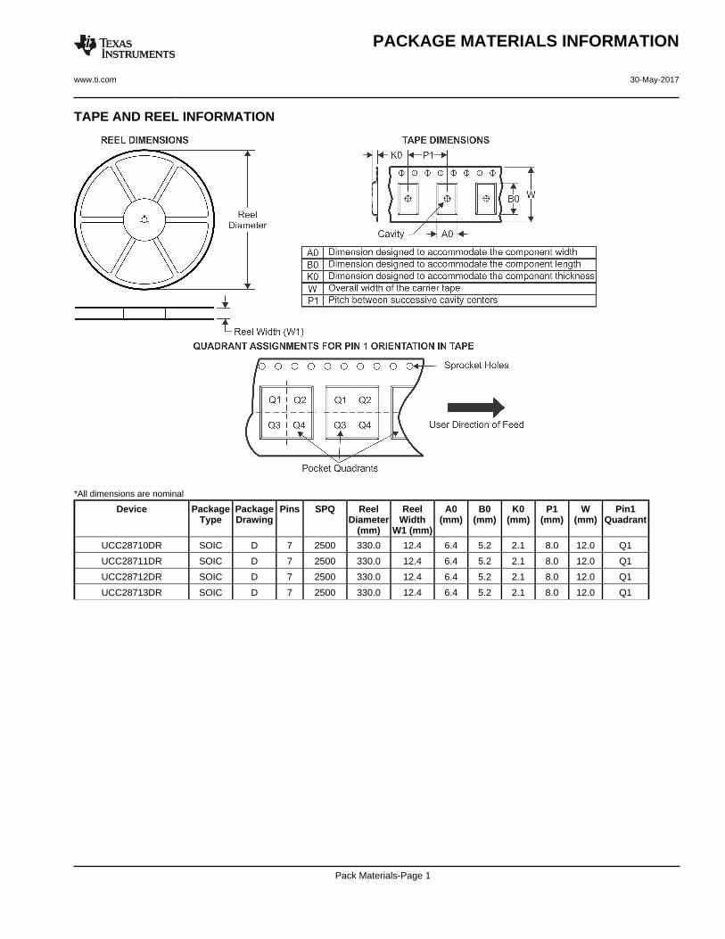
TAPE AND REEL INFORMATION
*All dimensions are nominal
Device PackageType
PackageDrawing
Pins SPQ ReelDiameter
(mm)
ReelWidth
W1 (mm)
A0(mm)
B0(mm)
K0(mm)
P1(mm)
W(mm)
Pin1Quadrant
UCC28710DR SOIC D 7 2500 330.0 12.4 6.4 5.2 2.1 8.0 12.0 Q1
UCC28711DR SOIC D 7 2500 330.0 12.4 6.4 5.2 2.1 8.0 12.0 Q1
UCC28712DR SOIC D 7 2500 330.0 12.4 6.4 5.2 2.1 8.0 12.0 Q1
UCC28713DR SOIC D 7 2500 330.0 12.4 6.4 5.2 2.1 8.0 12.0 Q1
PACKAGE MATERIALS INFORMATION
www.ti.com 30-May-2017
Pack Materials-Page 1
*All dimensions are nominal
Device Package Type Package Drawing Pins SPQ Length (mm) Width (mm) Height (mm)
UCC28710DR SOIC D 7 2500 367.0 367.0 35.0
UCC28711DR SOIC D 7 2500 367.0 367.0 35.0
UCC28712DR SOIC D 7 2500 367.0 367.0 35.0
UCC28713DR SOIC D 7 2500 367.0 367.0 35.0
PACKAGE MATERIALS INFORMATION
www.ti.com 30-May-2017
Pack Materials-Page 2
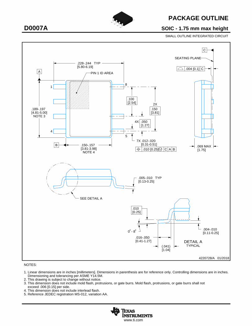
www.ti.com
PACKAGE OUTLINE
C
.228-.244 TYP[5.80-6.19]
.069 MAX[1.75]
.100[2.54]
7X .012-.020 [0.31-0.51]
2X.150[3.81]
.005-.010 TYP[0.13-0.25]
0 - 8 .004-.010[0.11-0.25]
.010[0.25]
.016-.050[0.41-1.27]
4X .050[1.27]
A
.189-.197[4.81-5.00]
NOTE 3
B .150-.157[3.81-3.98]
NOTE 4
(.041)[1.04]
SOIC - 1.75 mm max heightD0007ASMALL OUTLINE INTEGRATED CIRCUIT
4220728/A 01/2018
NOTES: 1. Linear dimensions are in inches [millimeters]. Dimensions in parenthesis are for reference only. Controlling dimensions are in inches. Dimensioning and tolerancing per ASME Y14.5M. 2. This drawing is subject to change without notice. 3. This dimension does not include mold flash, protrusions, or gate burrs. Mold flash, protrusions, or gate burrs shall not exceed .006 [0.15] per side. 4. This dimension does not include interlead flash.5. Reference JEDEC registration MS-012, variation AA.
18
.010 [0.25] C A B
54
PIN 1 ID AREA
SEATING PLANE
.004 [0.1] C
SEE DETAIL A
DETAIL ATYPICAL
SCALE 2.800
www.ti.com
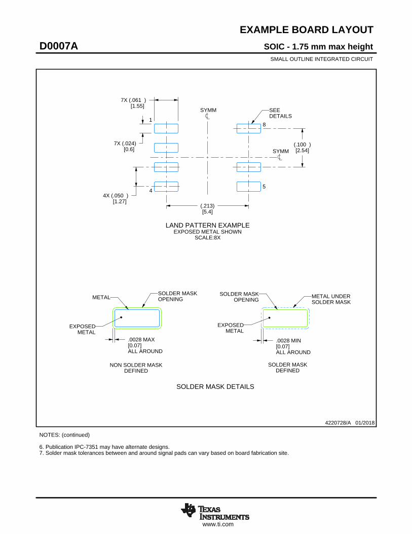
EXAMPLE BOARD LAYOUT
.0028 MAX[0.07]ALL AROUND
.0028 MIN[0.07]ALL AROUND
(.213)[5.4]
4X (.050 )[1.27]
7X (.061 )[1.55]
7X (.024)[0.6]
(.100 )[2.54]
SOIC - 1.75 mm max heightD0007ASMALL OUTLINE INTEGRATED CIRCUIT
4220728/A 01/2018
NOTES: (continued) 6. Publication IPC-7351 may have alternate designs. 7. Solder mask tolerances between and around signal pads can vary based on board fabrication site.
METALSOLDER MASKOPENING
NON SOLDER MASKDEFINED
SOLDER MASK DETAILS
EXPOSEDMETAL
OPENINGSOLDER MASK METAL UNDER
SOLDER MASK
SOLDER MASKDEFINED
EXPOSEDMETAL
LAND PATTERN EXAMPLEEXPOSED METAL SHOWN
SCALE:8X
SYMM
1
45
8
SEEDETAILS
SYMM

www.ti.com
EXAMPLE STENCIL DESIGN
7X (.061 )[1.55]
7X (.024)[0.6]
4X (.050 )[1.27]
(.213)[5.4]
(.100 )[2.54]
SOIC - 1.75 mm max heightD0007ASMALL OUTLINE INTEGRATED CIRCUIT
4220728/A 01/2018
NOTES: (continued) 8. Laser cutting apertures with trapezoidal walls and rounded corners may offer better paste release. IPC-7525 may have alternate design recommendations. 9. Board assembly site may have different recommendations for stencil design.
SOLDER PASTE EXAMPLEBASED ON .005 INCH [0.125 MM] THICK STENCIL
SCALE:8X
SYMM
SYMM
1
45
8

IMPORTANT NOTICE
Texas Instruments Incorporated (TI) reserves the right to make corrections, enhancements, improvements and other changes to itssemiconductor products and services per JESD46, latest issue, and to discontinue any product or service per JESD48, latest issue. Buyersshould obtain the latest relevant information before placing orders and should verify that such information is current and complete.TI’s published terms of sale for semiconductor products (http://www.ti.com/sc/docs/stdterms.htm) apply to the sale of packaged integratedcircuit products that TI has qualified and released to market. Additional terms may apply to the use or sale of other types of TI products andservices.Reproduction of significant portions of TI information in TI data sheets is permissible only if reproduction is without alteration and isaccompanied by all associated warranties, conditions, limitations, and notices. TI is not responsible or liable for such reproduceddocumentation. Information of third parties may be subject to additional restrictions. Resale of TI products or services with statementsdifferent from or beyond the parameters stated by TI for that product or service voids all express and any implied warranties for theassociated TI product or service and is an unfair and deceptive business practice. TI is not responsible or liable for any such statements.Buyers and others who are developing systems that incorporate TI products (collectively, “Designers”) understand and agree that Designersremain responsible for using their independent analysis, evaluation and judgment in designing their applications and that Designers havefull and exclusive responsibility to assure the safety of Designers' applications and compliance of their applications (and of all TI productsused in or for Designers’ applications) with all applicable regulations, laws and other applicable requirements. Designer represents that, withrespect to their applications, Designer has all the necessary expertise to create and implement safeguards that (1) anticipate dangerousconsequences of failures, (2) monitor failures and their consequences, and (3) lessen the likelihood of failures that might cause harm andtake appropriate actions. Designer agrees that prior to using or distributing any applications that include TI products, Designer willthoroughly test such applications and the functionality of such TI products as used in such applications.TI’s provision of technical, application or other design advice, quality characterization, reliability data or other services or information,including, but not limited to, reference designs and materials relating to evaluation modules, (collectively, “TI Resources”) are intended toassist designers who are developing applications that incorporate TI products; by downloading, accessing or using TI Resources in anyway, Designer (individually or, if Designer is acting on behalf of a company, Designer’s company) agrees to use any particular TI Resourcesolely for this purpose and subject to the terms of this Notice.TI’s provision of TI Resources does not expand or otherwise alter TI’s applicable published warranties or warranty disclaimers for TIproducts, and no additional obligations or liabilities arise from TI providing such TI Resources. TI reserves the right to make corrections,enhancements, improvements and other changes to its TI Resources. TI has not conducted any testing other than that specificallydescribed in the published documentation for a particular TI Resource.Designer is authorized to use, copy and modify any individual TI Resource only in connection with the development of applications thatinclude the TI product(s) identified in such TI Resource. NO OTHER LICENSE, EXPRESS OR IMPLIED, BY ESTOPPEL OR OTHERWISETO ANY OTHER TI INTELLECTUAL PROPERTY RIGHT, AND NO LICENSE TO ANY TECHNOLOGY OR INTELLECTUAL PROPERTYRIGHT OF TI OR ANY THIRD PARTY IS GRANTED HEREIN, including but not limited to any patent right, copyright, mask work right, orother intellectual property right relating to any combination, machine, or process in which TI products or services are used. Informationregarding or referencing third-party products or services does not constitute a license to use such products or services, or a warranty orendorsement thereof. Use of TI Resources may require a license from a third party under the patents or other intellectual property of thethird party, or a license from TI under the patents or other intellectual property of TI.TI RESOURCES ARE PROVIDED “AS IS” AND WITH ALL FAULTS. TI DISCLAIMS ALL OTHER WARRANTIES ORREPRESENTATIONS, EXPRESS OR IMPLIED, REGARDING RESOURCES OR USE THEREOF, INCLUDING BUT NOT LIMITED TOACCURACY OR COMPLETENESS, TITLE, ANY EPIDEMIC FAILURE WARRANTY AND ANY IMPLIED WARRANTIES OFMERCHANTABILITY, FITNESS FOR A PARTICULAR PURPOSE, AND NON-INFRINGEMENT OF ANY THIRD PARTY INTELLECTUALPROPERTY RIGHTS. TI SHALL NOT BE LIABLE FOR AND SHALL NOT DEFEND OR INDEMNIFY DESIGNER AGAINST ANY CLAIM,INCLUDING BUT NOT LIMITED TO ANY INFRINGEMENT CLAIM THAT RELATES TO OR IS BASED ON ANY COMBINATION OFPRODUCTS EVEN IF DESCRIBED IN TI RESOURCES OR OTHERWISE. IN NO EVENT SHALL TI BE LIABLE FOR ANY ACTUAL,DIRECT, SPECIAL, COLLATERAL, INDIRECT, PUNITIVE, INCIDENTAL, CONSEQUENTIAL OR EXEMPLARY DAMAGES INCONNECTION WITH OR ARISING OUT OF TI RESOURCES OR USE THEREOF, AND REGARDLESS OF WHETHER TI HAS BEENADVISED OF THE POSSIBILITY OF SUCH DAMAGES.Unless TI has explicitly designated an individual product as meeting the requirements of a particular industry standard (e.g., ISO/TS 16949and ISO 26262), TI is not responsible for any failure to meet such industry standard requirements.Where TI specifically promotes products as facilitating functional safety or as compliant with industry functional safety standards, suchproducts are intended to help enable customers to design and create their own applications that meet applicable functional safety standardsand requirements. Using products in an application does not by itself establish any safety features in the application. Designers mustensure compliance with safety-related requirements and standards applicable to their applications. Designer may not use any TI products inlife-critical medical equipment unless authorized officers of the parties have executed a special contract specifically governing such use.Life-critical medical equipment is medical equipment where failure of such equipment would cause serious bodily injury or death (e.g., lifesupport, pacemakers, defibrillators, heart pumps, neurostimulators, and implantables). Such equipment includes, without limitation, allmedical devices identified by the U.S. Food and Drug Administration as Class III devices and equivalent classifications outside the U.S.TI may expressly designate certain products as completing a particular qualification (e.g., Q100, Military Grade, or Enhanced Product).Designers agree that it has the necessary expertise to select the product with the appropriate qualification designation for their applicationsand that proper product selection is at Designers’ own risk. Designers are solely responsible for compliance with all legal and regulatoryrequirements in connection with such selection.Designer will fully indemnify TI and its representatives against any damages, costs, losses, and/or liabilities arising out of Designer’s non-compliance with the terms and provisions of this Notice.
Mailing Address: Texas Instruments, Post Office Box 655303, Dallas, Texas 75265Copyright © 2018, Texas Instruments Incorporated