tx26d12vm0apa · 2019. 10. 13. · kaohsiung hitachi electronics co., ltd. for messrs: date: jul....
TRANSCRIPT

KAOHSIUNG HITACHI ELECTRONICS CO., LTD.
FOR MESSRS: DATE: Jul. 07th 2009
CUSTOMER’S ACCEPTANCE SPECIFICATIONS
TX26D12VM0APA
Contents
No. ITEM SHEET No. PAGE
1 COVER 7B64PS 2701-TX26D12VM0APA-2 1-1/1
2 RECORD OF REVISION 7B64PS 2702-TX26D12VM0APA-2 2-1/1
3 GENERAL DATA 7B64PS 2703-TX26D12VM0APA-2 3-1/1
4 ABSOLUTE MAXIMUM RATINGS 7B64PS 2704-TX26D12VM0APA-2 4-1/1
5 ELECTRICAL CHARACTERISTICS 7B64PS 2705-TX26D12VM0APA-2 5-1/2~2/2
6 OPTICAL CHARACTERISTICS 7B64PS 2706-TX26D12VM0APA-2 6-1/2~2/2
7 BLOCK DIAGRAME 7B64PS 2707-TX26D12VM0APA-2 7-1/1
8 RELIABILITY TESTS 7B64PS 2708-TX26D12VM0APA-2 8-1/1
9 LCD INTERFACE 7B64PS 2709-TX26D12VM0APA-2 9-1/11~11/11
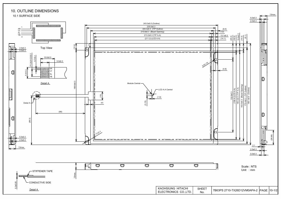
10 OUTLINE DIMENSIONS 7B63PS 2710-TX26D12VM0APA-2 10-1/2~2/2
11 TOUCH PANEL 7B64PS 2711-TX26D12VM0APA-2 11-1/2~2/2
12 APPEARANCE STANDARD 7B64PS 2712-TX26D12VM0APA-2 12-1/4~4/4
13 PRECAUTIONS 7B64PS 2713-TX26D12VM0APA-2 13-1/2~2/2
14 DESIGNATION OF LOT MARK 7B64PS 2714-TX26D12VM0APA-2 14-1/1
ACCEPTED BY: PROPOSED BY:
KAOHSIUNG HITACHI ELECTRONICS CO., LTD.
SHEET NO. 7B64PS 2701-TX26D12VM0APA-2 PAGE 1-1/1

2. RECORD OF REVISION
DATE SHEET No. SUMMARY 7B64PS 2703-
TX26D12VM0APA-2
PAGE 3-1/1
3.1 DISPLAY FEATURES
Revised
Power Consumption 7.68W → 8.04W
7B64PS 2705-
TX26D12VM0APA-2
PAGE 5-2/2
5.2 BACKLIGHT CHARACTERISTICS
Revised
Item Typ.
(660) LED Forward Current
(Dim Control) (30)
↓
Item Typ.
670 LED Forward Current
(Dim Control) 30
7B64PS 2706-
TX26D12VM0APA-2
PAGE 6-1/2
6 OPTICAL CHARACTERISTICS
7B63PS 2710-
TX26D12VM0APA-2
PAGE 10-1/2
10.1 SURFACE SIDE
All Sheet Revised.
Jul.07,’09
7B63PS 2710-
TX26D12VM0APA-2
PAGE 10-2/2
10.2 BACK SIDE
All Sheet Revised.
KAOHSIUNG HITACHI ELECTRONICS CO., LTD.
SHEET NO. 7B64PS 2702-TX26D12VM0APA-2 PAGE 2-1/1
ITEM SYMBOL CONDITION MIN. TYP. MAX.
x (0.57) (0.61) (0.67)Red
y (0.27) (0.36) (0.37)
x (0.25) (0.37) (0.35)Green
y (0.54) (0.59) (0.64)
x (0.09) (0.15) (0.19)Blue
y (0.05) (0.10) (0.15)
x (0.30) (0.35) (0.40)
Color
Chromaticity
Whitey
=0°,
θ=0°
(0.32) (0.37) (0.42)
↓
ITEM SYMBOL CONDITION MIN. TYP. MAX.
x 0.56 0.61 0.66 Red
y 0.31 0.36 0.41
x 0.32 0.37 0.42 Green
y 0.54 0.59 0.64
x 0.10 0.15 0.20 Blue
y 0.05 0.10 0.15
x 0.30 0.35 0.40
Color
Chromaticity
Whitey
=0°,
θ=0°
0.32 0.37 0.42

3. GENERAL DATA
3.1 DISPLAY FEATURES
This module is a 10.4” SVGA of 4:3 format amorphous silicon TFT.The pixel format is vertical stripe and sub pixels are arranged as R(red), G(green), B(blue) sequentially. This display is RoHS compliant, and COG (chip on glass) technology and LED backlight are applied on this display.
Part Name TX26D12VM0APA
Module Dimensions 243.0(W) mm x 185.1(H) mm x 13.0max (D) mm
LCD Active Area 211.2(W) mm x 158.4(H) mm
Dot Pitch 0.088(W) mm x 3(R, G, B)(W) x 0.264(H) mm
Resolution 800 x 3(RGB)(W) x 600(H) dots
Color Pixel Arrangement R, G, B Vertical stripe
LCD Type Transmissive Color TFT; Normally Black
Display Type Active Matrix
Number of Colors 16777k Colors(8-bit RGB)
Backlight 8 LEDs parallel x 3 serial (24 LEDs in total)
Weight (750) g (typ.)
Interface 1ch-LVDS/Receiver ; 20 pins
Power Supply Voltage 3.3V for LCD; 12V for Backlight
Power Consumption 1.221 W for LCD (SVGA) ;8.04W for backlight
Viewing Direction Super Wide Version (Horizontal and Vertical: 170°, CR 10)
Touch Panel Resistive type; Film on Glass; 4-wire type; Anti-glare surface
KAOHSIUNG HITACHI ELECTRONICS CO., LTD.
SHEET NO. 7B64PS 2703-TX26D12VM0APA-2 PAGE 3-1/1

4. ABSOLUTE MAXIMUM RATINGS
Item Symbol Min. Max. Unit Remarks
Supply Voltage VDD 0 4.0 V -
Input Voltage of Logic VI -0.3 VDD+0.3 V Note 1
Operating Temperature Top -20 70 C Note 2
Storage Temperature Tst -30 80 C Note 2
Forward Current IF - 120 mA LED Unit
Reverse Voltage VR - 3.65 V Note 3
Note 1: It shall be applied to pixel data signal and clock signal.
Note 2: The maximum rating is defined as above based on the temperature on the panel surface, which might be different from ambient temperature after assembling the panel into the application. Moreover, some temperature-related phenomenon as below needed to be noticed:
- Background color, contrast and response time would be different in temperatures other than 25 C .
- Operating under high temperature will shorten LED lifetime.
Note 3: Fig. 4.1 shows the maximum rating of LED forward current against temperature. The backlight unit in this display has been set to 80 mA per LED. This is within the range when operating the display between -20~70 C .
For the dimming function, reducing the LED backlight voltage 12V to the expected brightness is recommended. Alternatively, using PWM signal with 10KHz and 3.3V amplitude to dim by adjusting the duty ratio.
Fig. 4.1
KAOHSIUNG HITACHI ELECTRONICS CO., LTD.
SHEET NO. 7B64PS 2704-TX26D12VM0APA-2 PAGE 4-1/1
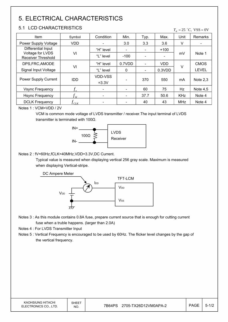
5. ELECTRICAL CHARACTERISTICS
5.1 LCD CHARACTERISTICS
Item Symbol Condition Min. Typ. Max. Unit Remarks
Power Supply Voltage VDD - 3.0 3.3 3.6 V -
“H” level - - +100 Differential Input Voltage for LVDS
Receiver Threshold VI
“L” level -100 - - mV Note 1
“H” level 0.7VDD - VDD DPS,FRC,AMODE
Signal Input Voltage VI
“L” level 0 - 0.3VDD V
CMOS
LEVEL
Power Supply Current IDD VDD-VSS
=3.3V - 370 550 mA Note 2,3
Vsync Frequency vf - - 60 75 Hz Note 4,5
Hsync Frequency Hf - - 37.7 50.6 KHz Note 4
DCLK Frequency CLKf - - 40 43 MHz Note 4
Notes 1 : VCM=VDD / 2V
VCM is common mode voltage of LVDS transmitter / receiver.The input terminal of LVDS
transmitter is terminated with 100Ω.
Notes 2 : fV=60Hz,fCLK=40MHz,VDD=3.3V,DC Current.
Typical value is measured when displaying vertical 256 gray scale. Maximum is measured
when displaying Vertical-stripe.
Notes 3 : As this module contains 0.8A fuse, prepare current source that is enough for cutting current
fuse when a truble happens. (larger than 2.0A)
Notes 4 : For LVDS Transmitter Input
Notes 5 : Vertical Frequency is encouraged to be used by 60Hz. The flicker level changes by the gap of
the vertical frequency.
0VVSS ,25 CTa
KAOHSIUNG HITACHI ELECTRONICS CO., LTD.
SHEET NO. 7B64PS 2705-TX26D12VM0APA-2 PAGE 5-1/2
LVDS
Receiver 100Ω
IN+
IN-
VDD
VSS
TFT-LCM DC Ampere Meter
IDD
VDD

5.2 BACKLIGHT CHARACTERISTICS
Item Symbol Condition Min. Typ. Max. Unit Remarks
LED Input Voltage VLED - 11.7 12.0 12.3 V Note1
0V; 0% duty - 670 - LED Forward Current
(Dim Control) ILED
3.3VDC; 100% duty - 30 - mA Note 2
LED lifetime - 640 mA - 70K - hrs Note 3
Note 1: As Fig. 5.1 shown, LED current is constant, 640 mA, controlled by the LED driver when applying 12V VLED.
Note 2: Dimming function can be obtained by applying DC voltage or PWM signal from the display interface CN1. The recommended PWM signal is 1K ~ 10K Hz with 3.3V amplitude.
Note 3: The estimated lifetime is specified as the time to reduce 50% brightness by applying 640 mA at 25 C .
Fig. 5.1
CTa25
KAOHSIUNG HITACHI ELECTRONICS CO., LTD.
SHEET NO. 7B64PS 2705-TX26D12VM0APA-2 PAGE 5-2/2
CTa25
20)
640mA
6. OPTICAL CHARACTERISTICS The optical characteristics are measured based on the conditions as below:
- Supplying the signals and voltages defined in the section of electrical characteristics.
- The backlight unit needs to be turned on for 30 minutes.
- The ambient temperature is 25 C .
- In the dark room around 500~1000 lx, the equipment has been set for the measurements as shown in Fig 6.1.
3.3V
Item Symbol Condition Min. Typ. Max. Unit Remarks
Brightness of White - 280 360 - 2cd/m Note 1
Brightness Uniformity - 75 - - % Note 2
Contrast Ratio CR
0 ,0 ,
ILED= 640 mA 500 800 - - Note 3
Response Time Rise + Fall 0 ,0 - 25 65 ms Note 4
NTSC Ratio - 0 ,0 - 60 - % -
x 10 CR ,0 - 85 -
x 10 CR ,180 - 85 -
y 10 CR ,90 - 85 - Viewing Angle
y 10 CR ,270 - 85 -
Degree Note 5
X 0.56 0.61 0.66 Red
Y 0.31 0.36 0.41
X 0.32 0.37 0.42 Green
Y 0.54 0.59 0.64
X 0.10 0.15 0.20 Blue
Y 0.05 0.10 0.15
X 0.30 0.35 0.40
Color
Chromaticity
White Y
0 ,0
0.32 0.37 0.42
- Note 6
Note 1: The brightness is measured from 9 point of the panel, P1~P9 in Fig. 6.2, for the average value.
Note 2: The brightness uniformity is calculated by the equation as below:
, which is based on the brightness values of the 9 points measured by BM-5 as shown in Fig. 6.2.
VDDHz, 60 25 va fCT ,
LCD panel
Photo detector:BM-5A
Field 1∘ Distance:500 mm
Fig. 6.1
P1
Y=600
X=450
Y=1200 Y=1800
X=300
X=150P4
P7
P2
P5
P8 P9
P6
P3
Dot(0,0)
Fig. 6.2
KAOHSIUNG HITACHI ELECTRONICS CO., LTD.
SHEET NO. 7B64PS 2706-TX26D12VM0APA-2 PAGE 6-1/2
Brightness uniformity = X100% Min. Brightness
Max. Brightness
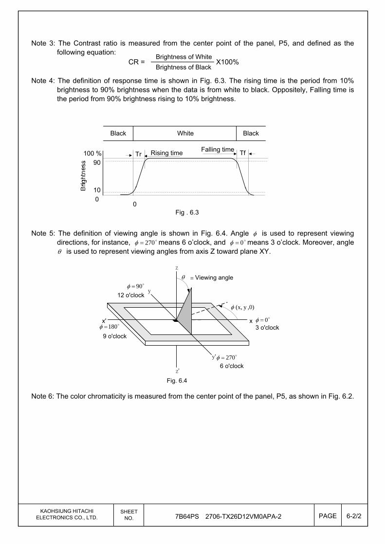
Note 3: The Contrast ratio is measured from the center point of the panel, P5, and defined as the following equation:
Note 4: The definition of response time is shown in Fig. 6.3. The rising time is the period from 10% brightness to 90% brightness when the data is from white to black. Oppositely, Falling time is the period from 90% brightness rising to 10% brightness.
BlackBlack White
0Fig . 6.3
Rising timeTr TfFalling time100 %
90
10
0
Note 5: The definition of viewing angle is shown in Fig. 6.4. Angle is used to represent viewing directions, for instance, 270 means 6 o’clock, and 0 means 3 o’clock. Moreover, angle is used to represent viewing angles from axis Z toward plane XY.
3 o'clockxx'
y
y'
z
z'
,0)y (x,
0
90
180
270 6 o'clock
12 o'clock
9 o'clock
= Viewing angle
Fig. 6.4
Note 6: The color chromaticity is measured from the center point of the panel, P5, as shown in Fig. 6.2.
KAOHSIUNG HITACHI ELECTRONICS CO., LTD.
SHEET NO. 7B64PS 2706-TX26D12VM0APA-2 PAGE 6-2/2
CR = X100% Brightness of White
Brightness of Black


8. RELIABILITY TESTS
Test Item Condition
High Temperature 1) Operating
2) 70 C 240 hrs
Low Temperature 1) Operating
2) -20 C 240 hrs
High Temperature 1) Storage
2) 80 C 240 hrs
Low Temperature 1) Storage
2) -30 C 240 hrs
Heat Cycle 1) Operating
2) –20 C ~70 C
3) 3hrs~1hr~3hrs 240 hrs
Thermal Shock 1) Non-Operating
2) -35 C 85 C
3) 0.5 hr 0.5 hr 240 hrs
High Temperature &
Humidity
1) Operating
2) 40 C & 85%RH
3) Without condensation
4) Note 3
240 hrs
Vibration
1) Non-Operating
2) 20~200 Hz
3) 2G
4) X, Y, and Z directions
1 hr for each direction
Mechanical Shock
1) Non-Operating
2) 10 ms
3) 50G
4) Y X, and Z directions
Once for each direction
ESD
1) Operating
2) Tip: 200 pF, 250
3) Air discharge for glass: 8KV
4) Contact discharge for metal frame: 8KV
5) Contact discharge for LCD interface: 100V
1) Glass: 9 points 2) Metal frame: 8 points3) Connector: all pins
Note 1: Display functionalities are inspected under the conditions defined in the specification after the reliability tests.
Note 2: The display is not guaranteed for use in corrosive gas environments.
Note 3: Under the condition of high temperature & humidity, if the temperature is higher than 40, the humidity needs to be reduced as Fig. 8.1 shown.
Rel
ativ
e H
umid
ity
RH
(%
)
0
10
20
30
4050
60
7080
90
20 25 30 35 40 45 50 55 60 65 70 75
Fig. 8.1
Temperature Ta C)(
KAOHSIUNG HITACHI ELECTRONICS CO., LTD.
SHEET NO. 7B64PS 2708-TX26D12VM0APA-2 PAGE 8-1/1

9. LCD INTERFACE
9.1 INTERFACE PIN CONNECTIONS
The display interface connector is FI-SEB20P-HF13E made by JAE and more details of the connector are shown
in the section of outline dimension.
Pin assignment of LCD interface is as below:
Pin No. Symbol Description Note 1 VDD
2 VDD Power Supply for Logic 1)
3 DPS Scan Direction Control (High : Reverse , Low : STD) 3) 4 VSS Ground (0V) 2) 5 IN0-
6 IN0+ Pixel Data
7 VSS Ground (0V) 2) 8 IN1-
9 IN1+ Pixel Data
10 VSS Ground (0V) 2)
11 IN2-
12 IN2+ Pixel Data
13 VSS Ground (0V) 2)
14 CLK IN-
15 CLK IN+ Clock
16 FRC High : 8bit , Low : 6bit 17 IN3-
18 IN3+ Pixel Data
19 AMODE LVDS Format Setting (Refer to P9-2/11)
20 DIM Normal Brightness:0V or 0% PWM Duty Brightness Control:0V to 3.3VDC or 0% to 100% PWM Duty.
Note 1) All VDD pins should be connected to +3.3V.
Note 2) All VSS pins should be connected to GND(0V),Metal bezel is connected internally to VSS.
Note3 ) Vertical Display Inode and Horizontal Display mode control
The backlight interface connector is SM08B-SRSS-TB made by JST, and pin assignment of backlight is as below:
Pin No. Signal Level Function
1~3 VLED+ - Power Supply for LED(12V)
4~5 NC - No Connection
6~8 VLED- - GND
KAOHSIUNG HITACHI ELECTRONICS CO., LTD.
SHEET NO. 7B64PS 2709-TX26D12VM0APA-2 PAGE 9-1/11
HITACHI
HITACHI
DPS : Low DPS : High
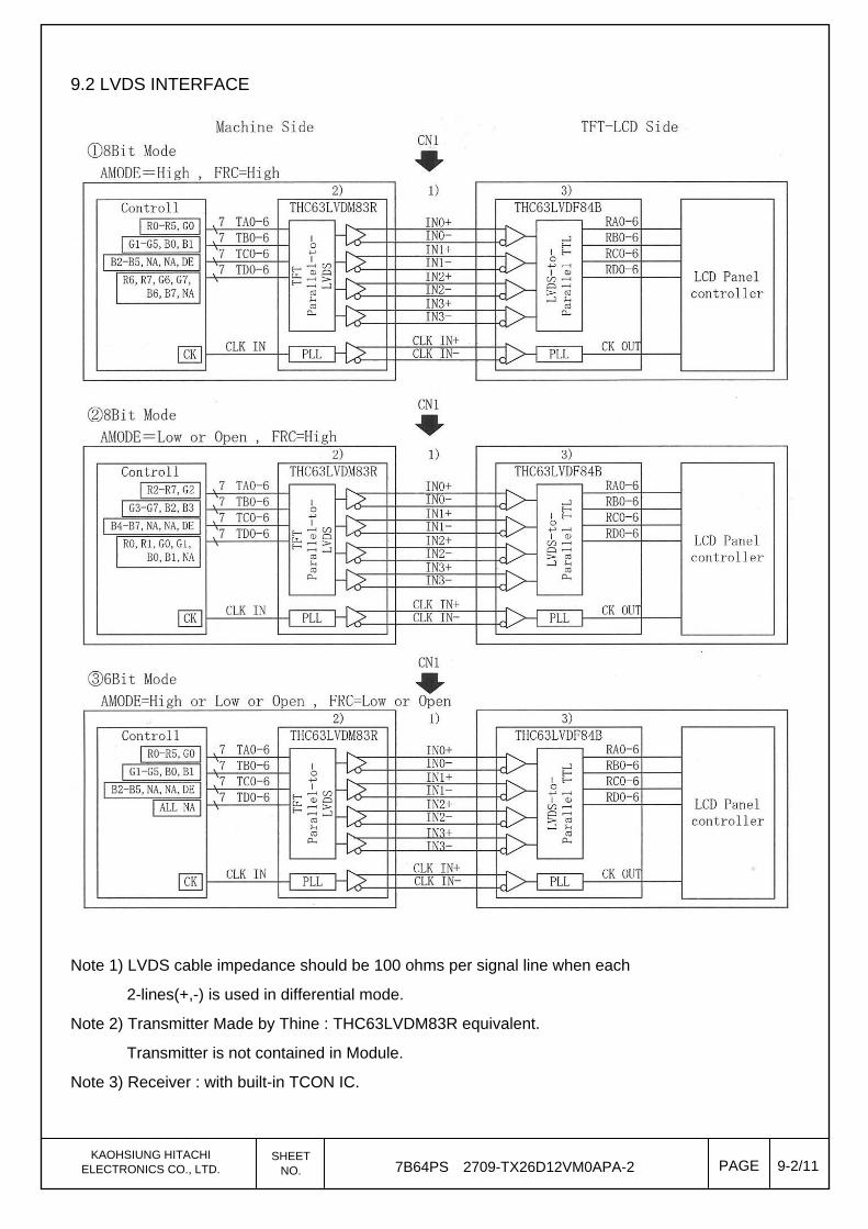
9.2 LVDS INTERFACE
Note 1) LVDS cable impedance should be 100 ohms per signal line when each
2-lines(+,-) is used in differential mode.
Note 2) Transmitter Made by Thine : THC63LVDM83R equivalent.
Transmitter is not contained in Module.
Note 3) Receiver : with built-in TCON IC.
KAOHSIUNG HITACHI ELECTRONICS CO., LTD.
SHEET NO. 7B64PS 2709-TX26D12VM0APA-2 PAGE 9-2/11

9.3 DATA MAPPING
1) 8 Bit Mode
Note : Assignment in the Mode A(THC63LVDM83R)
KAOHSIUNG HITACHI ELECTRONICS CO., LTD.
SHEET NO. 7B64PS 2709-TX26D12VM0APA-2 PAGE 9-3/11

KAOHSIUNG HITACHI ELECTRONICS CO., LTD.
SHEET NO. 7B64PS 2709-TX26D12VM0APA-2 PAGE 9-4/11

2) 6 Bit Mode
Note : Assignment in the Mode A(THC63LVDM83R)
KAOHSIUNG HITACHI ELECTRONICS CO., LTD.
SHEET NO. 7B64PS 2709-TX26D12VM0APA-2 PAGE 9-5/11
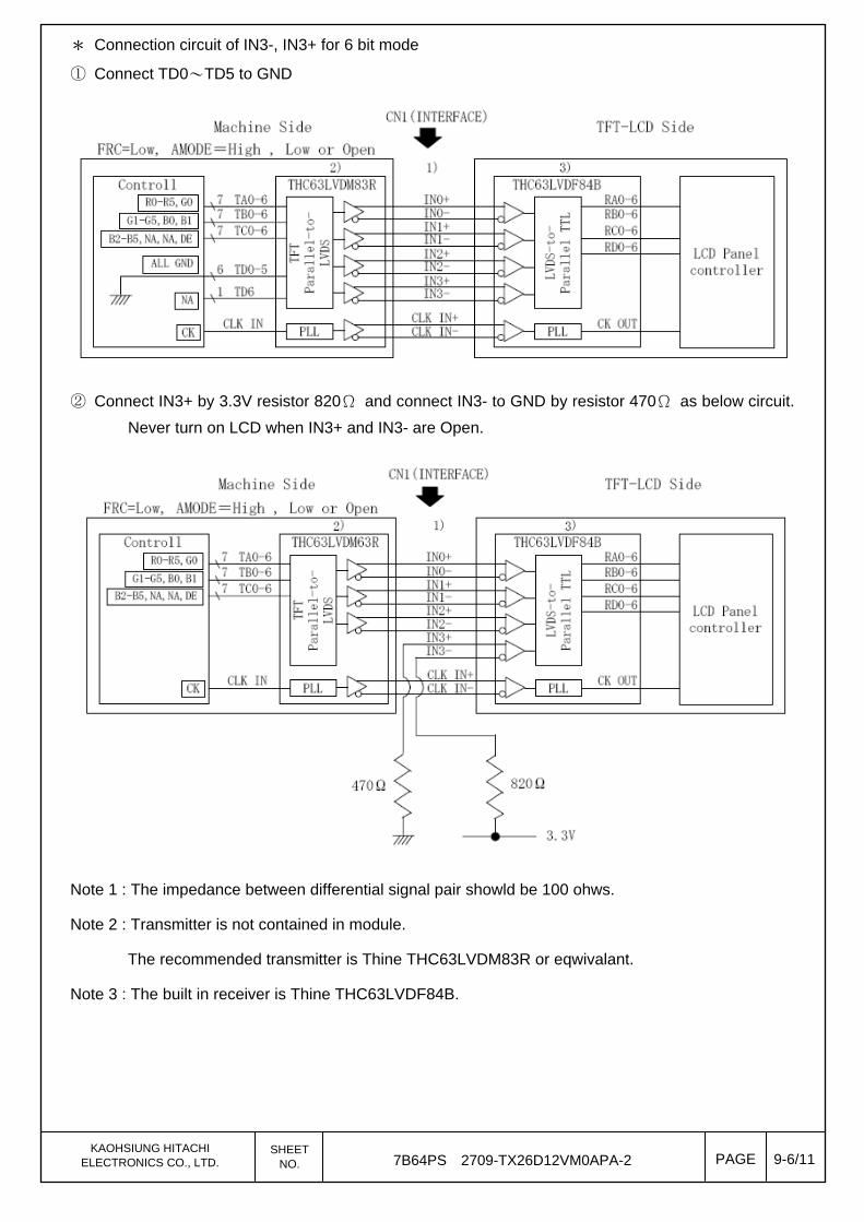
* Connection circuit of IN3-, IN3+ for 6 bit mode
① Connect TD0~TD5 to GND
② Connect IN3+ by 3.3V resistor 820Ω and connect IN3- to GND by resistor 470Ω as below circuit.
Never turn on LCD when IN3+ and IN3- are Open.
Note 1 : The impedance between differential signal pair showld be 100 ohws.
Note 2 : Transmitter is not contained in module.
The recommended transmitter is Thine THC63LVDM83R or eqwivalant.
Note 3 : The built in receiver is Thine THC63LVDF84B.
KAOHSIUNG HITACHI ELECTRONICS CO., LTD.
SHEET NO. 7B64PS 2709-TX26D12VM0APA-2 PAGE 9-6/11
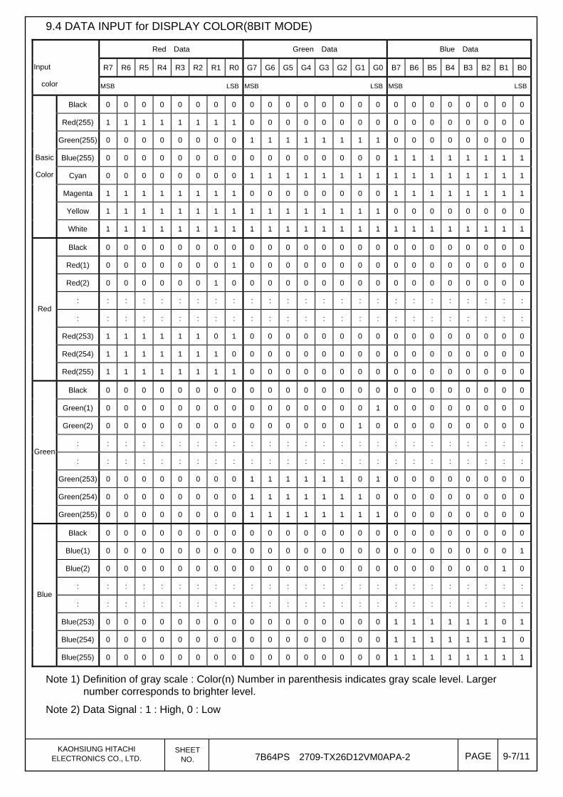
9.4 DATA INPUT for DISPLAY COLOR(8BIT MODE)
Red Data Green Data Blue Data
R7 R6 R5 R4 R3 R2 R1 R0 G7 G6 G5 G4 G3 G2 G1 G0 B7 B6 B5 B4 B3 B2 B1 B0
Input
color MSB LSB MSB LSB MSB LSB
Black 0 0 0 0 0 0 0 0 0 0 0 0 0 0 0 0 0 0 0 0 0 0 0 0
Red(255) 1 1 1 1 1 1 1 1 0 0 0 0 0 0 0 0 0 0 0 0 0 0 0 0
Green(255) 0 0 0 0 0 0 0 0 1 1 1 1 1 1 1 1 0 0 0 0 0 0 0 0
Blue(255) 0 0 0 0 0 0 0 0 0 0 0 0 0 0 0 0 1 1 1 1 1 1 1 1
Cyan 0 0 0 0 0 0 0 0 1 1 1 1 1 1 1 1 1 1 1 1 1 1 1 1
Magenta 1 1 1 1 1 1 1 1 0 0 0 0 0 0 0 0 1 1 1 1 1 1 1 1
Yellow 1 1 1 1 1 1 1 1 1 1 1 1 1 1 1 1 0 0 0 0 0 0 0 0
Basic
Color
White 1 1 1 1 1 1 1 1 1 1 1 1 1 1 1 1 1 1 1 1 1 1 1 1
Black 0 0 0 0 0 0 0 0 0 0 0 0 0 0 0 0 0 0 0 0 0 0 0 0
Red(1) 0 0 0 0 0 0 0 1 0 0 0 0 0 0 0 0 0 0 0 0 0 0 0 0
Red(2) 0 0 0 0 0 0 1 0 0 0 0 0 0 0 0 0 0 0 0 0 0 0 0 0
: : : : : : : : : : : : : : : : : : : : : : : : :
: : : : : : : : : : : : : : : : : : : : : : : : :
Red(253) 1 1 1 1 1 1 0 1 0 0 0 0 0 0 0 0 0 0 0 0 0 0 0 0
Red(254) 1 1 1 1 1 1 1 0 0 0 0 0 0 0 0 0 0 0 0 0 0 0 0 0
Red
Red(255) 1 1 1 1 1 1 1 1 0 0 0 0 0 0 0 0 0 0 0 0 0 0 0 0
Black 0 0 0 0 0 0 0 0 0 0 0 0 0 0 0 0 0 0 0 0 0 0 0 0
Green(1) 0 0 0 0 0 0 0 0 0 0 0 0 0 0 0 1 0 0 0 0 0 0 0 0
Green(2) 0 0 0 0 0 0 0 0 0 0 0 0 0 0 1 0 0 0 0 0 0 0 0 0
: : : : : : : : : : : : : : : : : : : : : : : : :
: : : : : : : : : : : : : : : : : : : : : : : : :
Green(253) 0 0 0 0 0 0 0 0 1 1 1 1 1 1 0 1 0 0 0 0 0 0 0 0
Green(254) 0 0 0 0 0 0 0 0 1 1 1 1 1 1 1 0 0 0 0 0 0 0 0 0
Green
Green(255) 0 0 0 0 0 0 0 0 1 1 1 1 1 1 1 1 0 0 0 0 0 0 0 0
Black 0 0 0 0 0 0 0 0 0 0 0 0 0 0 0 0 0 0 0 0 0 0 0 0
Blue(1) 0 0 0 0 0 0 0 0 0 0 0 0 0 0 0 0 0 0 0 0 0 0 0 1
Blue(2) 0 0 0 0 0 0 0 0 0 0 0 0 0 0 0 0 0 0 0 0 0 0 1 0
: : : : : : : : : : : : : : : : : : : : : : : : :
: : : : : : : : : : : : : : : : : : : : : : : : :
Blue(253) 0 0 0 0 0 0 0 0 0 0 0 0 0 0 0 0 1 1 1 1 1 1 0 1
Blue(254) 0 0 0 0 0 0 0 0 0 0 0 0 0 0 0 0 1 1 1 1 1 1 1 0
Blue
Blue(255) 0 0 0 0 0 0 0 0 0 0 0 0 0 0 0 0 1 1 1 1 1 1 1 1
Note 1) Definition of gray scale : Color(n) Number in parenthesis indicates gray scale level. Larger number corresponds to brighter level.
Note 2) Data Signal : 1 : High, 0 : Low
KAOHSIUNG HITACHI ELECTRONICS CO., LTD.
SHEET NO. 7B64PS 2709-TX26D12VM0APA-2 PAGE 9-7/11

(6BIT MODE)
Red Data Green Data Blue Data
R5 R4 R3 R2 R1 R0 G5 G4 G3 G2 G1 G0 B5 B4 B3 B2 B1 B0
Input
color MSB LSB MSB LSB MSB LSB
Black 0 0 0 0 0 0 0 0 0 0 0 0 0 0 0 0 0 0
Red(63) 1 1 1 1 1 1 0 0 0 0 0 0 0 0 0 0 0 0
Green(63) 0 0 0 0 0 0 1 1 1 1 1 1 0 0 0 0 0 0
Blue(63) 0 0 0 0 0 0 0 0 0 0 0 0 1 1 1 1 1 1
Cyan 0 0 0 0 0 0 1 1 1 1 1 1 1 1 1 1 1 1
Magenta 1 1 1 1 1 1 0 0 0 0 0 0 1 1 1 1 1 1
Yellow 1 1 1 1 1 1 1 1 1 1 1 1 0 0 0 0 0 0
Basic
Color
White 1 1 1 1 1 1 1 1 1 1 1 1 1 1 1 1 1 1
Black 0 0 0 0 0 0 0 0 0 0 0 0 0 0 0 0 0 0
Red(1) 0 0 0 0 0 1 0 0 0 0 0 0 0 0 0 0 0 0
Red(2) 0 0 0 0 1 0 0 0 0 0 0 0 0 0 0 0 0 0
: : : : : : : : : : : : : : : : : : :
: : : : : : : : : : : : : : : : : : :
Red(61) 1 1 1 1 0 1 0 0 0 0 0 0 0 0 0 0 0 0
Red(62) 1 1 1 1 1 0 0 0 0 0 0 0 0 0 0 0 0 0
Red
Red(63) 1 1 1 1 1 1 0 0 0 0 0 0 0 0 0 0 0 0
Black 0 0 0 0 0 0 0 0 0 0 0 0 0 0 0 0 0 0
Green(1) 0 0 0 0 0 0 0 0 0 0 0 1 0 0 0 0 0 0
Green(2) 0 0 0 0 0 0 0 0 0 0 1 0 0 0 0 0 0 0
: : : : : : : : : : : : : : : : : : :
: : : : : : : : : : : : : : : : : : :
Green(61) 0 0 0 0 0 0 1 1 1 1 0 1 0 0 0 0 0 0
Green(62) 0 0 0 0 0 0 1 1 1 1 1 0 0 0 0 0 0 0
Green
Green(63) 0 0 0 0 0 0 1 1 1 1 1 1 0 0 0 0 0 0
Black 0 0 0 0 0 0 0 0 0 0 0 0 0 0 0 0 0 0
Blue(1) 0 0 0 0 0 0 0 0 0 0 0 0 0 0 0 0 0 1
Blue(2) 0 0 0 0 0 0 0 0 0 0 0 0 0 0 0 0 1 0
: : : : : : : : : : : : : : : : : : :
: : : : : : : : : : : : : : : : : : :
Blue(61) 0 0 0 0 0 0 0 0 0 0 0 0 1 1 1 1 0 1
Blue(62) 0 0 0 0 0 0 0 0 0 0 0 0 1 1 1 1 1 0
Blue
Blue(63) 0 0 0 0 0 0 0 0 0 0 0 0 1 1 1 1 1 1
Note 1) Definition of gray scale : Color(n) Number in parenthesis indicates gray scale level. Larger number corresponds to brighter level.
Note 2) Data Signal : 1 : High, 0 : Low
KAOHSIUNG HITACHI ELECTRONICS CO., LTD.
SHEET NO. 7B64PS 2709-TX26D12VM0APA-2 PAGE 9-8/11

9.5 INTERFACE TIMING
(1) LVDS Receiver Timing
(Interface of TFT module)
Item Symbol Min. Typ. Max. Unit Note
DCLK FREQUENCY 1/tcLK 35 40 45 MHz
0 data position tRP0 1/7*tCLK –0.49 1/7*tCLK 1/7*tCLK +0.49
1st data position tRP1 -0.49 0 +0.49
2nd data position tRP2 6/7*tCLK –0.49 6/7*tCLK 6/7*tCLK +0.49
3rd data position tRP3 5/7*tCLK –0.49 5/7*tCLK 5/7*tCLK +0.49
4th data position tRP4 4/7*tCLK –0.49 4/7*tCLK 4/7*tCLK +0.49
5th data position tRP5 3/7*tCLK –0.49 3/7*tCLK 3/7*tCLK +0.49
RinX
(X=0,1,2)
6th data position tRP6 2/7*tCLK –0.49 2/7*tCLK 2/7*tCLK +0.49
ns
KAOHSIUNG HITACHI ELECTRONICS CO., LTD.
SHEET NO. 7B64PS 2709-TX26D12VM0APA-2 PAGE 9-9/11
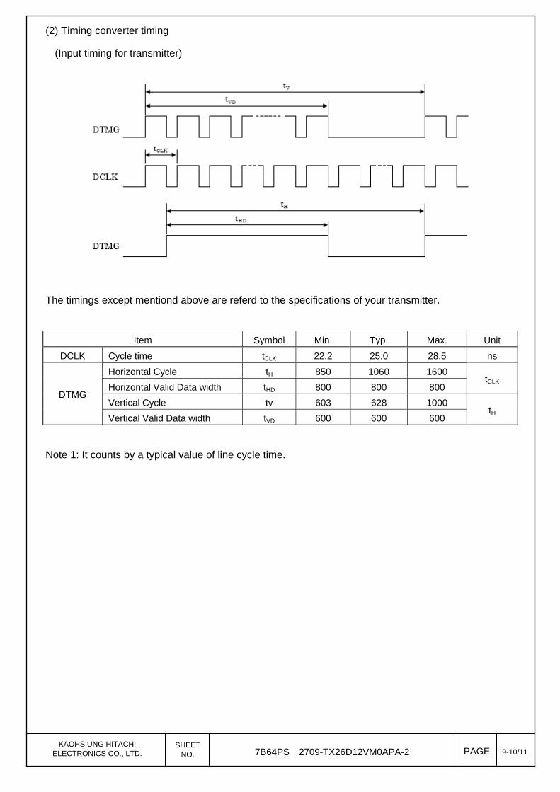
(2) Timing converter timing
(Input timing for transmitter)
The timings except mentiond above are referd to the specifications of your transmitter.
Item Symbol Min. Typ. Max. Unit
DCLK Cycle time tCLK 22.2 25.0 28.5 ns
Horizontal Cycle tH 850 1060 1600
Horizontal Valid Data width tHD 800 800 800 tCLK
Vertical Cycle tv 603 628 1000 DTMG
Vertical Valid Data width tVD 600 600 600 tH
Note 1: It counts by a typical value of line cycle time.
KAOHSIUNG HITACHI ELECTRONICS CO., LTD.
SHEET NO. 7B64PS 2709-TX26D12VM0APA-2 PAGE 9-10/11

(3) TIMING BETWEEN INTERFACE SIGNAL AND POWER SUPPLY
Power Supply, Input Signal and Backlight Voltage ON/OFF/REENTRY should comply with the following
sequence.
Note 1: In order to prevent electronic parts from destruction caused by latch-up, please input signal after Power Supply Voltage ON. In addition, please turn off signals before power supply voltage OFF.
Note 2: In order to prevent from function error due to residual charge, please reenter power supply voltage after time stipulated with t7.
Note 3: Please turn on Backlight after signals fix and turn off before signals down, otherwise noise appears in the display. The noise cause no problem with display performance in case of timing sequence comply with the spec.
KAOHSIUNG HITACHI ELECTRONICS CO., LTD.
SHEET NO. 7B64PS 2709-TX26D12VM0APA-2 PAGE 9-11/11

11. TOUCH PANEL The type of touch panel used on this display is resistive, analog, 4-wire and film on glass, and more characteristics are shown as below:
11.1 OPERATING CONDITIONS
Item Specification Remarks
Operating Voltage 5VDC -
11.2 ELECTRICAL CHARACTERISTICS
Item Specification Remarks
X1-X2 250~900Ω Resistance
Between Terminal Y1-Y2 210~600Ω -
Insulation Resistance X-Y 20MΩmin. At 25V DC
X ±1.5% max. Linearity
Y ±1.5% max. Note 1
Chattering 10ms max. -
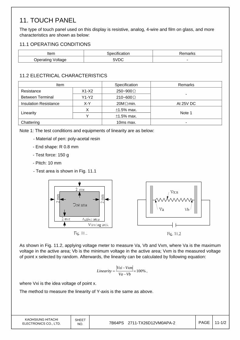
Note 1: The test conditions and equipments of linearity are as below:
- Material of pen: poly-acetal resin
- End shape: R 0.8 mm
- Test force: 150 g
- Pitch: 10 mm
- Test area is shown in Fig. 11.1
2 m
m
2 m
m
As shown in Fig. 11.2, applying voltage meter to measure Va, Vb and Vxm, where Va is the maximum voltage in the active area; Vb is the minimum voltage in the active area; Vxm is the measured voltage of point x selected by random. Afterwards, the linearity can be calculated by following equation:
%100
VbVa
VxmVxiLinearity ,
where Vxi is the idea voltage of point x.
The method to measure the linearity of Y-axis is the same as above.
KAOHSIUNG HITACHI ELECTRONICS CO., LTD.
SHEET NO. 7B64PS 2711-TX26D12VM0APA-2 PAGE 11-1/2
11.3 MECHANICAL CHARACTERISTICS
Item Specification Remarks
Pen Input Pressure 1.2N max. R0.8, Polyacetal Pen
Finger 1.2N max. R8.0, Silicon Rubber
Surface Hardness 3H min. JIS K 5400
11.4 OPTICAL CHARACTERISTICS
Item Specification Remarks
Transmittance 78% min. -
11.5 SAFETY AND ATTENTIONS
1) Do not put heavy shock or stress on the touch panel.
2) Please use soft cloth or absorbent cotton with ethanol to clean the touch panel by gently wiping. Moreover, please wipe it by horizontal or vertical direction instead of circling to prevent leaving scars on the touch panel’s surface.
3) Do not use any harmful chemicals such as acetone, toluene, and isopropyl alcohol to clean the display’s surface.
KAOHSIUNG HITACHI ELECTRONICS CO., LTD.
SHEET NO. 7B64PS 2711-TX26D12VM0APA-2 PAGE 11-2/2

12. APPEARANCE STANDARD The appearance inspection is performed in a dark room around 1200 lx based on the conditions as below:
- The distance between inspector’s eyes and display is 30 cm.
- The viewing zone is defined with angle shown in Fig. 12.1 The inspection should be performed within 45∘when display is shut down. The inspection should be performed within 5∘when display is power on.
Fig. 12.1
12.1 THE DEFINITION OF LCD ZONE
LCD panel is divided into 3 areas as shown in Fig.12.2 for appearance specification in next section. A zone is the LCD active area (dot area); B zone is the area, which extended 1 mm out from LCD active area; C zone is the area between B zone and metal frame.
In terms of housing design, B zone is the recommended window area customers’ housing should be located in.
Fig. 12.2
A zone
B zoneC zone
Metal frame
1 mm
KAOHSIUNG HITACHI ELECTRONICS CO., LTD.
SHEET NO. 7B64PS 2712-TX26D12VM0APA-2 PAGE 12-1/4

12.2 LCD APPEARANCE SPECIFICATION
The specification as below is defined as the amount of unexpected phenomenon or material in different zones of LCD panel. The definitions of length, width and average diameter using in the table are shown in Fig. 12.3 and Fig. 12.4.
Item Criteria Applied zone
Length (mm) Width (mm) Maximum number Minimum space
Ignored W≦0.02 Ignored -
L≦40 0.02<W≦0.04 10 - Scratches
L≦20 W≦0.04 10 -
A,B
Dent Distinguished one is acceptable
(To be judged by HITACHI standard) A
Wrinkles in polarizer Same as above A
Average diameter (mm) Maximum number
D≦0.3 Ignored
0.3<D≦0.5 10
0.5<D≦1.0 5
Bubbles on polarizer
1.0<D none
A
Filamentous (Line shape)
Length (mm) Width (mm) Maximum number
L : Ignored W≦0.06 Ignored
L≦1.0 Ignored
1.0<L 0.06<W
(See Dot shape)
A,B
Round (Dot shape)
Average diameter (mm) Maximum number Minimum Space
D≦0.45 Ignored -
0.45<D≦0.7 5 -
0.7<D none -
1) Stains
2) Foreign Materials
3) Dark Spot
Those wiped out easily are acceptable
A,B
Color Tone To be judged by HITACHI STANDARD A
Color Uniformity Sane as above A
Type Maximum number
1 dot 4
2 dot 2 Bright dot-defect
In total 6
1 dot 5
2 dot 2 Dark dot-defect
In total 5
Dot-Defect
(Note 1)
In total 11
A
KAOHSIUNG HITACHI ELECTRONICS CO., LTD.
SHEET NO. 7B64PS 2712-TX26D12VM0APA-2 PAGE 12-2/4

Note 1: The definitions of dot defect are as below:
- The defect area of the dot must be bigger than half of a dot.
- For bright dot-defect, showing black pattern, the dot’s brightness must be over 30% brighter than others.
- For dark dot-defect, showing white pattern, the dot’s brightness must be under 70% darker than others.
- The definition of 1-dot-defect is the defect-dot, which is isolated and no adjacent defect-dot.
- The definition of adjacent dot is shown as Fig. 12.5.
- The Density of dot defect is defined in the area within diameter =20mm.
A
The dots colored gray are adjacent to defect-dot A.
Fig. 12.5
KAOHSIUNG HITACHI ELECTRONICS CO., LTD.
SHEET NO. 7B64PS 2712-TX26D12VM0APA-2 PAGE 12-3/4
Fig 12.3
Wid
th Lenght
Fig 12.4
a
b
Average diameter = a+b
2
12.3 TOUCH PANEL APPEARANCE SPECIFICATION
The specification as below is defined by the amount of unexpected material in different zones of touch panel.
Item Criteria Applied zone Width (mm) Length (mm) Maximum number
W>0.1 L≧10 Not allowed 0.10≧W>0.05 10>L 4 pcs max.
Scratches
0.05≧W 10>L Ignored
A
Filamentous (Line shape) Width (mm) Length (mm) Maximum number
W>0.05 3<L Not allowed 0.05≧W 3≧L Ignored
A
Round (Dot shape) Average diameter (mm) Maximum number
D>0.35 Not allowed 0.35≧D>0.25 6 pcs max.
Foreign Materials
0.25>D Ignored
A
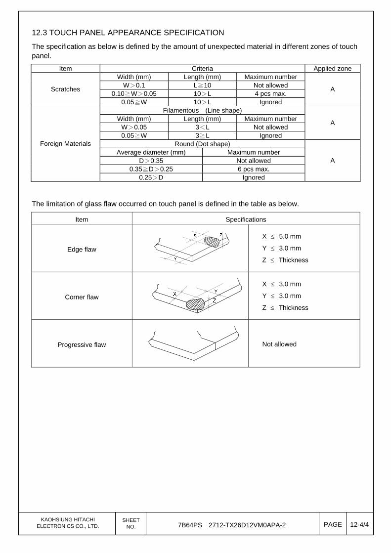
The limitation of glass flaw occurred on touch panel is defined in the table as below.
Item Specifications
Edge flaw
X 5.0 mm
Y 3.0 mm
Z Thickness
Corner flaw
X 3.0 mm
Y 3.0 mm
Z Thickness
Progressive flaw
Not allowed
KAOHSIUNG HITACHI ELECTRONICS CO., LTD.
SHEET NO. 7B64PS 2712-TX26D12VM0APA-2 PAGE 12-4/4

13. PRECAUTIONS
13.1 PRECAUTIONS of MOUNTING
1) Please refer to Fig. 13.1 for housing the display with touch panel into applications. The Fig. 13.1 shows some points as below:
- The cushion needs to be designed between housing and touch panel in order to avoid unexpected pressure to cause any wrong reactions, and the cushion should be located in the insulated area.
- The housing should not cover the active area of touch panel as the figure shown.
Fig 13.1
13.2 PRECAUTIONS of ESD
1) Before handling the display, please ensure your body has been connected to ground to avoid any damages by ESD. Also, do not touch display’s interface directly when assembling.
2) Please remove the protection film very slowly before turning on the display to avoid generating ESD.
13.3 PRECAUTIONS of HANDLING
1) In order to keep the appearance of display in good condition, please do not rub any surfaces of the displays by sharp tools harder than 3H, especially touch panel, metal frame and polarizer.
2) Please do not pile the displays in order to avoid any scars leaving on the display. In order to avoid any injuries, please pay more attention for the edges of glasses and metal frame, and wear finger cots to protect yourself and the display before working on it.
3) Touching the display area or the terminal pins with bare hand is prohibited. This is because it will stain the display area and cause poor insulation between terminal pins, and might affect display’s electrical characteristics furthermore.
4) Do not use any harmful chemicals such as acetone, toluene, and isopropyl alcohol to clean display’s surfaces.
5) Please use soft cloth or absorbent cotton with ethanol to clean the display by gently wiping. Moreover, when wiping the display, please wipe it by horizontal or vertical direction instead of circling to prevent leaving scars on the display’s surface, especially polarizer.
KAOHSIUNG HITACHI ELECTRONICS CO., LTD.
SHEET NO. 7B64PS 2713-TX26D12VM0APA-2 PAGE 13-1/2
Effective area (>3.0)
Transparent area Cushion
Tape
LCM
>0.
3
Case
Case
Case opening
Touch Panel
Insulated area

6) Please wipe any unknown liquids immediately such as saliva, water or dew on the display to avoid color fading or any permanently damages.
7) Maximum pressure to the surface of the display must be less than 410 x 1,96 Pa. If the area of adding pressure is less than 1 2cm , the maximum pressure must be less than 1.96N.
13.4 PRECAUTIONS OF OPERATING
1) Please input signals and voltages to the displays according to the values defined in the section of electrical characteristics to obtain the best performance. Any voltages over than absolute maximum rating will cause permanent damages to this display. Also, any timing of the signals out of this specification would cause unexpected performance.
2) When the display is operating at significant low temperature, the response time will be slower than it at 25 C . In high temperature, the color will be slightly dark and blue compared to original pattern. However, these are temperature-related phenomenon of LCD and it will not cause permanent damages to the display when used within the operating temperature.
3) The use of screen saver or sleep mode is recommended when static images are likely for long periods of time. This is to avoid the possibility of image sticking.
4) Spike noise can cause malfunction of the circuit. The recommended limitation of spike noise is no bigger than 100 mV.
13.5 PRECAUTIONS of STORAGE
If the displays are going to be stored for years, please be aware the following notices.
1) Please store the displays in a dark room to avoid any damages from sunlight and other sources of UV light.
2) The recommended long term storage temperature is between 10 C ~35 C and 55%~75% humidity to avoid causing bubbles between polarizer and LCD glasses, and polarizer peeling from LCD glasses.
3) It would be better to keep the displays in the container, which is shipped from Hitachi, and do not unpack it.
4) Please do not stick any labels on the display surface for a long time, especially on the polarizer.
KAOHSIUNG HITACHI ELECTRONICS CO., LTD.
SHEET NO. 7B64PS 2713-TX26D12VM0APA-2 PAGE 13-2/2

14. DESIGNATION of LOT MARK 1) The lot mark is showing in Fig.14.1. First 4 digits are used to represent production lot, T represented
made in Taiwan, and the last 6 digits are the serial number.
2) The tables as below are showing what the first 4 digits of lot mark are shorted for.
3) Except letters I and O, revision number will be showen on lot mark and following letters A to Z.
4) The location of the lot mark is on the back of the display shown in Fig. 14.1.
Fig 14.1
KAOHSIUNG HITACHI ELECTRONICS CO., LTD.
SHEET NO. 7B64PS 2714-TX26D12VM0APA-2 PAGE 14-1/1
Year Mark
2008 8
2009 9
2010 0
2011 1
2012 2
Month Mark Month Mark
1 01 7 07
2 02 8 08
3 03 9 09
4 04 10 10
5 05 11 11
6 06 12 12
Week (Days) Mark
1~7 1
8~14 2
15~21 3
22~28 4
29~31 5
9 0 5 1 T 0 0 0 0 0 1
T : Made in Taiwan Serial number
Week
Month
Year