two-dimensional transient simulation of the …€¦ · turn-off behavior of a planar...
TRANSCRIPT

Solid-State Electronics Vol. 32, No. 9, pp. 685-709, 1989 0038-1101/89 $3.00+0.00 Printed in Great Britain. All rights reserved Copyright © 1989 Maxwell Pergamon Macmillan pie
TWO-DIMENSIONAL TRANSIENT SIMULATION OF THE TURN-OFF BEHAVIOR OF A PLANAR MOS-TRANSISTOR
W. KAUSEL, H. POETZL, G. NANZ and S. SELBERHERR
Institut fiir Allgemeine Elektrotechnik und Elektronik, Department for CAE, Technical University of Vienna, Gul3hausstral3e 27-29, A-1040 Vienna, Austria
(Received 12 February 1988; in revised form 6 January 1989)
Abstraet--A two-dimensional transient simulation of the turn off behavior of a short channel NMOS transistor with Leer = 0.68 #m and dox = I00 A, has been carried out with the simulation program BAMBI. For the first time an external drain resistor is accounted for in this fast switching calculation. The computation starts with a steady state bias point in the triode region. The gate voltage is pulsed from Vg, = 5 V to V~ = 0 V immediately.
The paper presents the transient response of all physical quantities during the time after the switching. The simulation shows how the inversion layer is slowly reduced from both the source and the drain side whereas the lateral space-charge regions of both reverse biased pn-junctions build up quickly. Even at a time when lateral current has already vanished, electrons still remain in the channel region. They diffuse into the bulk, although the channel length is very short in comparison to the bulk depth. The electrons in the bulk slowly vanish by recombination.
It should be pointed out, that our results are based on a totally selfconsistent solution.
i. INTRODUCTION The switching behavior of MOS-transistors is of considerable interest because of a wealth of work aimed at the increase of integrated circuit switching speeds.
Therefore many transient analyses and analytical models have been published, that describe and ex- plain what happens during the switching process of MOS-transistors[l-3]. These publications deal with transistors with long channel lengths or work out one dimensional models, which loose validity for channel length shorter than 3 Itm.
In contrast this paper is the first to present the switching process for a realistic short channel device. We shall show the results of a complete transient 2-D simulation of a MOS-transistor with oxide thickness do~= 100/~, channel doping under the oxide NA = 1.10tVcm -3 and substrate doping NA = 6.1015 cm -3. With a gate length of L = 0 .85#m and a lateral extension of the drain and source diffusion areas of AL = 85 nm under the gate contact the transistor has an effective channel length of Le~= L - 2 . A L = 0.68 #m. Both diffusion areas have a depth of 227 nm. The doping profile is seen in Fig. 1. The lateral direction corresponds to the x-coordinate. The vertical direction corresponds to the y-coordinate. The threshold voltage of the device is V~ = 0.8 V.
Our analysis has been carried out by applying the 2-D device simulator BAMBI[4] which solves the three basic semiconductor eqns (1)-(3) together with the two transport eqns (4) and (5) discretized on a rectangular grid.
At# = - q (p - n + N D - N ~ , ) (1) E
(0,) v J , = - q ~ + R, (3)
J. = q D . V n - ql~.nVqJ (4)
Jp = - q D , Vp - ql.t,p VO. (5)
The local discretization is accomplished by means of the method of Finite Boxes[5]: lines are terminated in regions where the discretization error becomes small enough, so that no additional discretization points in those regions are necessary to obtain the accuracy required for the calculations. Hence the number of discretization points could be dramatically reduced compared to the method of finite differences. The three basic semiconductor equations are solved simultaneously by a Newton-iterat ion algorithm which guarantees a totally selfconsistent solution. Time discretization is accomplished by the fully implicit backward-Euler method[6,7].
The transient calculation starts at a bias point in the ohmic part of the l~Vd-characteristic with V,s = 5 V gate-source voltage and Vsb = 0 V source-- bulk voltage. The supply voltage of 5 V is applied to the drain contact by including a serial resistor of 8 k£1. The drain current is about 0.5 mA and thus, the drain-source voltage is about Vd, ~ 1 V. Using that steady-state start solution the simulation was started with a gate--voltage ramp down from V~ = 5 V to Vgs = 0 V within 50 ps (Fig. 2) obtaining the contact current characteristics of Fig. 3. Two major effects can be observed namely a sign reversal of the
685

686 W. KAUSEL et al.
%' k w.,,
-c;~. %
Fig. 1. Doping profile of the simulated structure (channel region).
D R A I N A N D G A T E V O L T A G E
5 Ix ' 4
' 'x× ~ o DRAIN VOLTAGE O1'-"-I 2 'Xxx, ~ ' , x / x GATE VOLTAGE
> 1
~ X'~x 0
= I t t : : : : : : : : : : : : : : : : : : : : : : : : : : : : : : : : : : : : : : : : : : : : 0 10 20 30 40 50 60 70 80 90 100 110 120
T [ M E ( p s )
Fig. 2. Voltage of the drain contact and the gate contact vs time.
CONTACT C U R R E N T S
o SOURCE CURRENT (p.A) ~ x x x ~ × x x ~ , N q , x [bRAIN CURRENT(/~A)
~ . .~ , - ,oo<~"~ ~, BULK CURRENT(/~A*IO) 400 '
I-- Z ILl --200 n- n- .:D - 4 0 0 0
- 6 0 0
. . . . . . I ",n..J....k,, I L I L I t I t I 0 10 20 30 40 50 60 70 80 90 100110 120
T I M E (ps)
Fig. 3. Terminal currents vs time during and after the gate voltage ramp.

Turn-off behavior of a planar MOS-transistor 687
SOURCE CURRENT
150
lOO
~ ~o
o b . i i i I I 50 6 o 70 8o 90 l o o lao ~2o
T I M E ( p s )
Fig. 4. Source contact current vs time after the gate voltage ramp.
bulk current after 33 ps and a sign reversal of the source current after the end of the gate-voltage ramp (Fig. 4). In order to separate the inherent transient processes in the channel region from the influence of the gate voltage ramp we decided to simulate the process with an almost abrupt gate-voltage pulse. Being aware of the fact that we use an unrealistic steep ramp we pulsed the gate voltage immediately down from V~s = 5 to Vgs = 0 V, a value beyond the threshold voltage. The transient response to that pulse has been simulated with time steps of 0.5 ps in the beginning increasing up to 10 ps at the end of the computation.
In the following chapters we present the transient behavior of all interesting physical quantities (i.e. electron and hole concentration, potential, field, electron and hole current densities).
2. ELECTRON DISTRIBUTION
The well known steady-state electron distribution of the channel region before switching makes it obvious that the amount of negative storage charge between source and drain under the channel is quite high (Fig. 5). Therefore it can be expected that the turn-off behavior will be mainly influenced by diffusion and recombination. This has been proved by our simulation.
Already the figure after 1 ps (Fig. 6) shows that electrons are diffusing back into the bulk. This diffusion process takes place on the source side of the channel region only.
Besides this diffusion current, a lateral field forces the electrons to flow into the drain and source diffusion regions on both sides of the channel and consequently the inversion layer shows a reduction in concentration on both sides compared to the level in the center. However, the drain current is limited due to the drain resistor. Thus, the pinch off on the source side is significantly higher. The high field currents on both sides of the channel give rise to the positive contact current at source and drain. Positive contact
current means that the electrons are flowing out of the device.
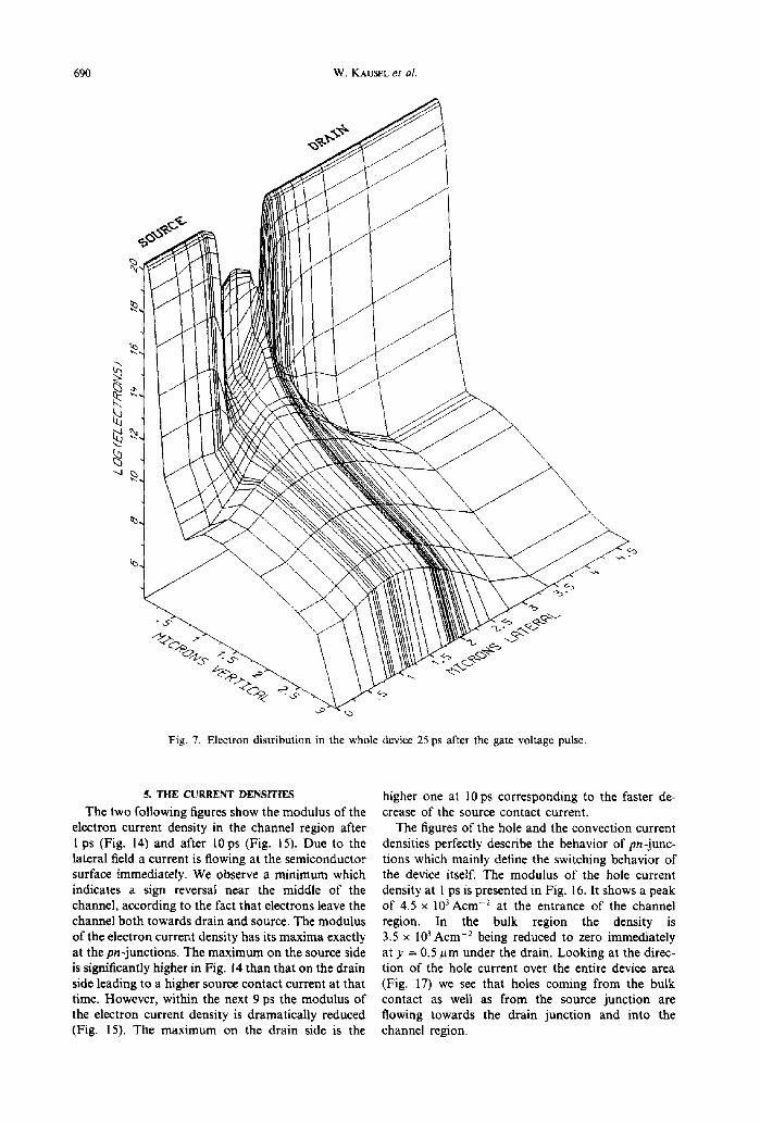
After 25 ps the process has continued and it can be seen, that more electrons are now flowing towards drain according to the high electric field. The channel is deeply pinched off on the drain side (Fig. 7). The diffusion has carried on and distributed the minorities over the bulk where they slowly vanish by recombina- tion. The diffusion process has obviously decreased on the source side whereas it has developed on the drain side of the channel region. The following figures prove that the process slows down significantly since the field current rapidly decreases and diffusion becomes more and more dominant.
After more than 100 ps the field current has com- pletely vanished. At that time no contact current is flowing but the electron concentration in the channel region is still up to 1012cm -3 under the gate and about 4 magnitudes higher in the bulk than in steady-state condition (Fig. 8). The carrier lifetime now determines when the equilibrium concentration will be reached by recombination.
3. HOLE DISTRIBUTION
At the bias point in the triode region the entire area between source and drain is totally depleted from holes according to the high vertical field (Fig. 9). The space charge region of the drain-bulk diode can clearly be seen. Immediately after the voltage pulse the holes diffuse towards the semiconductor surface to fill up the depletion region under the gate since the inversion field decreases. The holes flow towards the semiconductor-oxide interface with the dielectric time constant z, = E/a ~0 .13ps and form an elec- tron-hole plasma there. The figure at 10 ps shows a significant rise of the hole concentration up to 106 cm -3 after the switching (Fig. 10).
A time constant of r(t)= C(t)'Rb > l ps is valid from now on slowing down that process. This be- comes apparent from figures that are not included because of space limitations.
Two major effects can be studied now. Comparing the hole concentration of Fig. 10 with that of Fig. 9 a hole injection from bulk into the drain region can be observed indicating a forward biased drain-bulk diode. This indeed is confirmed by the value of the drain-source voltage of Vd, = - 0 . 8 V at 10ps. On the other hand the source-bulk diode reacts as a reverse biased pn-junction showing an increasing depletion.
This situation has completely changed after 25 ps (Fig. 11). A depletion process between drain and bulk has started as well as between drain and the channel region. With Vd, = 1.9 V at the drain contact the drain-bulk diode actually is reverse biased. Looking at the source-bulk diode we now recognize hole injection from the bulk there. The hole concentration in the channel region has reached a value of 101° cm -3 immediately under the oxide interface and a maxi-

688 W. KAUSEL et al.
"-d
° ,..¢,
"~'<<"~F'/-.
Fig. 5. Steady-state electron distribution in the whole device before switching.
mum of 5 x 1026 cm -3 a little bit deeper under the surface due to the channel doping.
Figure 12 shows the hole distribution in the chan- nel region after 100 ps. The concentration under the oxide semiconductor interface has been further in- creased to 4 x 1014cm -3. The distribution in the channel region still shows a depletion under the gate due to the gate voltage of 0 V compared with the flat-band voltage of - 0 . 3 V.
Depletion at the drain-bulk diode has further continued and a deep depletion region has been established around the drain diffusion area.
On the other hand the process has turned again at the source-bulk diode and we see depletion there as well. Both charge pumping effects concerning the drain-bulk diode and the source-bulk diode will be further explained by the following chapters.
4. P O T E N T I A L A N D E L E C T R I C F I E L D
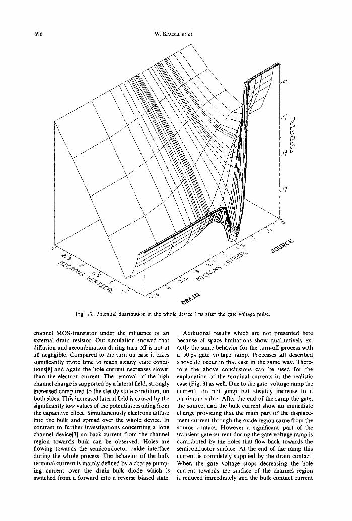
Figure 13 presents the potential distribution imme- diately after the gate voltage pulse. Compared with the steady-state condition before switching it shows a significant change after 1 ps. The potential jumps with the voltage pulse from positive to negative values, reaches - 3 V at drain and even - 3 . 8 V in the middle of the channel region (Fig. 13). The explana- tion for this dramatic behavior is the capacitive effect by the gate potential which lowers the potential of the channel region and the drain voltage as well as the potential between source and bulk. Neither the homogeneous potential drop over the whole channel region according to the homogeneous negative stor- age charge nor the voltage drop over the space-charge region between drain and bulk has been changed. As

Turn-off behavior of a planar MOS-transistor 689
Fig. 6. Electron distribution in the whole device 1 ps after the gate voltage pulse.
a result the potential distribution over the entire device area (Fig. 13) shows significant minima.
Since the source voltage remains constant the electric field showing from source to the channel region is dramatically increased causing a high lateral displacement and field current in negative x-direction that results in a high positive current peak at the source contact (Fig. 27). The space charge region between source and the channel region builds up very quickly. The field on the drain side remains constant still showing from drain to the channel region. Last but not least a field in negative y-direction has been formed in the bulk region that is relatively high compared with the steady-state situation.
Additional results not presented in that paper show the steady increase of the drain voltage which finally
reaches 5 V as well as the slow flattening of the potential distribution within the channel region and the region between source and bulk. Thus, the inver- sion field steadily decreases, the field between drain and the channel region increases whereas that one between source and the channel region is reduced at the same time. The displacement currents over both space charge regions are therefore flowing in negative x-direction after 3 ps. That means that the displace- ment current has changed sign on the source side of the channel region very quickly.
The potential minimum between source and bulk turns into a maximum after 25 ps thus initiating an oscillation process.
The behavior of the potential directly defines and explains the switching behavior of that device.
690 W. KAUSEL et al.
r•q-
,i
",,5"
.%-
~¢'4'~, "~ -- ~"~-
Fig. 7. Electron distribution in the whole device 25 ps after the gate voltage pulse.
5. THE CURRENT DENSITIES
The two following figures show the modulus of the electron current density in the channel region after 1 ps (Fig. 14) and after 10ps (Fig. 15). Due to the lateral field a current is flowing at the semiconductor surface immediately. We observe a min imum which indicates a sign reversal near the middle of the channel, according to the fact that electrons leave the channel both towards drain and source. The modulus of the electron current density has its maxima exactly at the p n - j u n c t i o n s . The maximum on the source side is significantly higher in Fig. 14 than that on the drain side leading to a higher source contact current at that time. However, within the next 9 ps the modulus of the electron current density is dramatically reduced (Fig. 15). The maximum on the drain side is the
higher one at 10 ps corresponding to the faster de- crease of the source contact current.
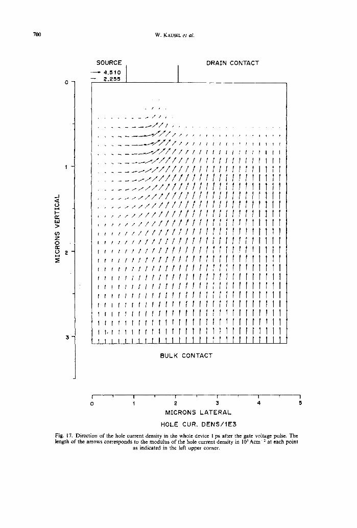
The figures of the hole and the convection current densities perfectly describe the behavior of pn-junc- tions which mainly define the switching behavior of the device itself. The modulus of the hole current density at 1 ps is presented in Fig. 16. It shows a peak of 4.5 × 10³ Acm -2 at the entrance of the channel region. In the bulk region the density is 3.5 × 10 3 Acm -2 being reduced to zero immediately at y --- 0.5 # m under the drain. Looking at the direc- tion of the hole current over the entire device area (Fig. 17) we see that holes coming from the bulk contact as well as from the source junct ion are flowing towards the drain junct ion and into the channel region.

Turn-off behavior of a planar MOS-transistor 691
-%-
",S"
..-~°
Fig. 8. Electron distribution in the whole device 100 ps after the gate voltage pulse.
To explain the current flow the direction of the total convection current at l ps is presented in Fig. 18. The source-bulk diode is reverse biased. A displacement current in positive y-direction passes the junction and continues as hole field current. Following the lateral field the hole current flows towards the channel region and the drain junction•
With Vds = - 3 V the drain-bulk diode is strongly forward biased. Since the field changes sign at y =0.9/~m the hole field current continues as diffusion and displacement current. A hole and electron injection from both sides respectively reduces the space charge region and the field• Thus, the displacement current in negative y-direction causes a corresponding electron current within the drain diffusion region that supports the reduction of the channel charge on the one hand and flows out of the
drain contact on the other hand. Consequently we recognize a sign reversal of the contact current density at x = 2.6 gm at the drain contact. Since the current from the channel region is several magnitudes higher we still have positive drain current.
Within the channel we recognize the high lateral field current and the vertical diffusion current as described above.
Two picosecond later (at 3 ps) the situation has changed at the source diode (Fig. 19). The field, still having a positive y-component as far as y = 1.2 #m, is decreasing now. Thus, the displacement current has changed its sign flowing into negative y-direction. Within the bulk it overcompensates the hole current that flows in opposite direction, passes the space charge region and continues as electron current beyond the junction wi th in the source diffusion

692 W. KAUSEL et al.
.5
It0
Q
Fig. 9. Steady-state hole distribution in the channel region before switching.
region. The source electron current completely flows into the channel region at 3 ps.
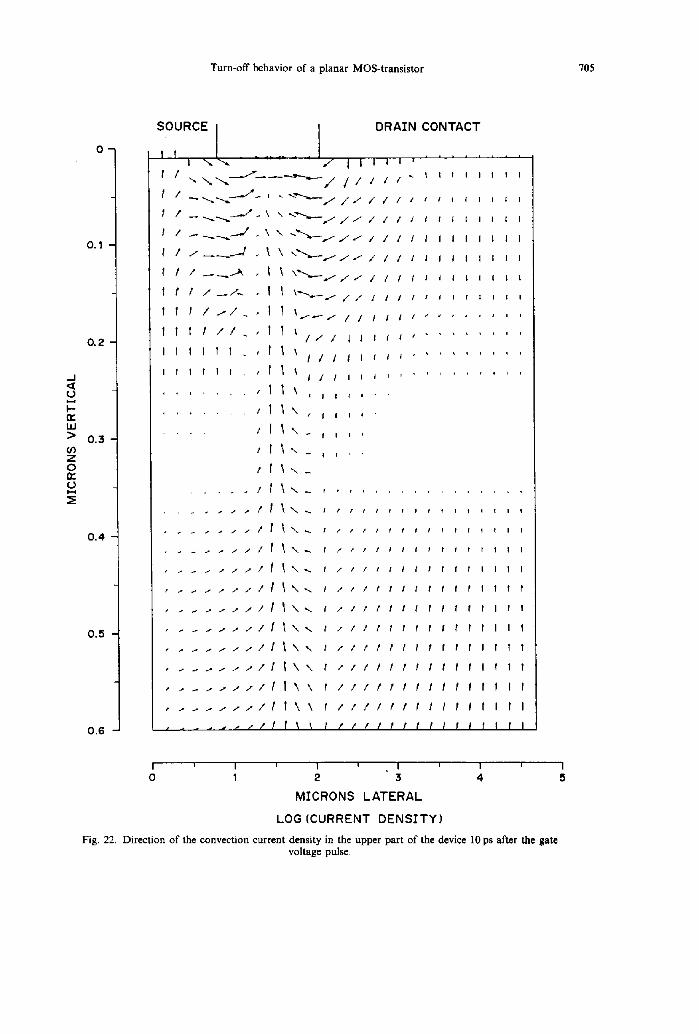
At 10ps the bulk contact current has almost reached its zero crossing. The modulus of the hole current density shows its strong reduction in the bulk as well as in the channel region. However, the peak has moved towards the surface (Fig. 20). Holes are flowing from the bulk contact towards both junctions and into the channel region (Fig. 21). The source- bulk junction now acts as a forward biased diode (Fig. 22). Carriers are injected from both sides respec- tively and space charge region and field are further decreased. The negative displacement current con- tinues as electron current and partially reaches the
source contact. We recognize a sign reversal of th~ current density at the source contact at x ~ 0.5 #m
The negative current densities at the drain contac have vanished completely in the meantime. Thq voltage drop in the space charge region has bee1 reduced to the built-in voltage of 0.5 V. At 10 p space charge region and field are already increasinl as indicated by the electron current flowing fror drain towards the junction. This current continues a displacement current over the space charge regio according to the increasing field. It overcompensate the negative hole field current within the bulk, tur towards the channel region and continues as a hol current towards the interface. Beneath the junctio

Turn-off behavior of a planar MOS-transistor 693
.,.0
5
~,.-v
• -t.. ,q.X,- %'x~
Fig. I0. Hole distribution in the channel region 10ps after the gate voltage pulse.
holes flow towards drain due to the small but still existing negative field in the bulk region.
At 25 ps the bulk contact current reaches its nega- tive maximum. The hole current density peak within the channel region, situated significantly closer to the surface again, has been increased from 2 x 10³ Acm -2 to 2.5 x 10³ Acm -2 (Fig. 23). The figure of the hole current direction (Fig. 24) shows that the drain junction acts as a hole current source, thus speeding up the injection of holes into the depletion region at the surface of the channel region. The hole current is flowing into the channel region and to the bulk contact as well as towards the source junction.
The potential shows a slight maximum at
y = 1.5/zm between source and bulk at 25 ps. Thus, the resulting field causes a field current towards the source junction. The source-bulk diode is still for- ward biased (Fig, 25). The main part of the diode current reaches the source contact causing negative source contact current at 25 ps (Fig. 27).
With Vds = 1.9 V the drain-bulk diode is strongly reverse biased (Fig. 25). The resulting diode switch- off current removes the storage charge and builds up the space charge region steadily. Thus, the field is increased until the voltage drop of 5 V is finally reached at the end of the switching process. The current passes the junction as displacement current thus supporting the hole diffusion current in the

694 W. KAUSEL et al.
.¢
.5
.#
~ c,a
oo ~
Fig. l 1. Hole distribution in the channel region 25 ps after the gate voltage pulse.
channel region on the one hand and causing the negative source and bulk contact currents on the other hand.
6. DRAIN VOLTAGE AND CONTACT CURRENTS
In steady-state condition prior to the switching, the drain voltage was V d = 1 V corresponding to the drain current o f I d = 0.5 mA. Due to capacitive effects the drain voltage jumps to - 3 V (Fig. 26). Increasing almost exponentially to the final value of 5 V it reaches 90% after 60 ps with the zero crossing at 14 ps.
Looking at the terminal currents (Fig. 27) we see that source-, drain- and bulk-contact currents are
flowing into the device summing up to a high dis- placement current that passes the oxide and flows out of the gate contact.
The source current has a high peak due to the strong field increase between source and the channel region and the corresponding displacement current over the space charge region. This displacement current decreases quickly. Changing its sign after 3 ps it reduces the source terminal current. Thus, the source current shows a significantly small time con- stant. It becomes smaller than the drain current after 6 ps at a time when the drain voltage still is below zero. Since the currents strongly deviate from a single exponential behavior it is difficult to obtain relevant time constants. For the source current a time con- stant of approximately zl = 4ps seems appropriate

Turn-off behavior of a planar MOS-transistor 695
,4
.to
~t:~,,5~ -z'%"
~-~,~-d~,~.~ ~.x- "~
Fig. 12. Hole distribution in the channel region 100 ps after the gate voltage pulse•
while the decrease of drain current is considerably slower.
The gate current is a pure displacement current that crosses the oxide region. Since it corresponds to the source current in the beginning it shows a corre- sponding high negative peak and a similar time constant. After the disappearance of the source cur- rent it simply represents the continuation across the oxide region of the hole and electron current into the channel region.
The drain current initially jumps by a factor two to ld = 1 mA. Its time constant is about z2 = 32 ps corresponding to the drain resistor of 8 kfl.
The negative bulk current after the zero crossing at exactly 12 ps originates from the hole charge in the drain-bulk diode and is not caused by a hole reflow
from the channel region (Fig. 24). It is rather related to the zero crossing of the drain voltage which takes place at 14 ps and the subsequent switch off of the drain-bulk diode. This behavior is distinctly different from the switching processes of long channel devices[3].
Finally the enlarged figure of the source current shows how the terminal current follows the potential oscillations at the source-bulk diode (Fig. 28). It shows its first zero crossing after 25 ps followed by further sign reversals after 49, 81 and 96 ps.
7. CONCLUSIONS
This paper presents for the first time a complete history of all events during the turn off of a short
696 W. KAUSEL et al.
, 0
c" ,f
- c ~ - , s - ~ "~
Fig. 13. Potential distribution in the whole device 1 ps after the gate voltage pulse.
channel MOS-transistor under the influence of an external drain resistor. Our simulation showed that diffusion and recombination during turn off is not at all negligible. Compared to the turn on case it takes significantly more time to reach steady state condi- tions[8] and again the hole current decreases slower than the electron current. The removal of the high channel charge is supported by a lateral field, strongly increased compared to the steady state condition, on both sides. This increased lateral field is caused by the significantly low values of the potential resulting from the capacitive effect. Simultaneously electrons diffuse into the bulk and spread over the whole device. In contrast to further investigations concerning a long channel device[3] no back-current from the channel region towards bulk can be observed. Holes are flowing towards the semiconductor-oxide interface during the whole process. The behavior of the bulk terminal current is mainly defined by a charge pump- ing current over the drain-bulk diode which is switched from a forward into a reverse biased state.
Additional results which are not presented here because of space limitations show qualitatively ex- actly the same behavior for the turn-off process with a 50 ps gate-voltage ramp. Processes all described above do occur in that case in the same way. There- fore the above conclusions can be used for the explanation of the terminal currents in the realistic case (Fig. 3) as well. Due to the gate-voltage ramp the currents do not jump but steadily increase to a maximum value. After the end of the ramp the gate, the source, and the bulk current show an immediate change providing that the main part of the displace- ment current through the oxide region came from the source contact. However a significant part of the transient gate current during the gate voltage ramp is contributed by the holes that flow back towards the semiconductor surface. At the end of the ramp this current is completely supplied by the drain contact. When the gate voltage stops decreasing the hole current towards the surface of the channel region is reduced immediately and the bulk contact current

Turn-off behavior of a planar MOS-transistor 697
t~,
c: b
q / -
Fig. 14, Modulus of electron current density in the channel region 1 ps after the gate voltage pulse.

698 W. KAUSEL et al.
"L,
Fig. 15. Modulus of electron current density in the channel region 10ps after the gate voltage pulse.

Turn-off behavior of a planar MOS-transistor 699
,.P
c ,Q
...p. °
Fig. 16. Modulus of hole current density in the whole device I ps after the gate voltage pulse.
SSE 32/9---B
700 W. ](AUSEL et al.
O
1
i
o I,-4
I - t r I,LI >
Z 0 t r t,.J 2 - !-,,4 ~l
3
SOURCE
• " 4 . 5 1 0 l 2 . 2 5 5
DRAIN CONTACT
. I t
. . . . . . . . I I ,
. . . . . . . t / / / . . . . . . . . . . . . . . . . .
. _ _ _ . ~ / / / I ~ . . . . . . . . . . . . . . .
_ . ~ ' / / / / / / I I I I i t r r t t i , , ,
. . . . . 7 / / / I I 7 f I I t I t t t t t i i I i
. . . . . ~ / / / l l l i l f r t t t t t t t t I I
. . . . t / / / l l l l l l f f t t t t t t l i l l
. . . . ~ / / / / l l l i l t t f t t t t t r l l l
. . . . ~ / / l l l l l l l t t l l t l l l l l l l
. . . ~ / / l l l l l l l f f f t t t t t f t l l
. . . . ~ / / i l l l l l l f f t t t t t t t t l l
. . . . / / / l l l l l l l f t t t f t t t t t l l , , , / / 7 / / l l l l l f t t t t t t t f l l l l
, , / / / i l l l l l t t t t t t t t t t r l l l , , / / l l l l l i l f t f t t t t t t t r l l l t~ l l l l l t t l f t f t t t t t t t r l l f ~ ~ l i l l l l f t l t t t t t t t f l l l l
~ / i i t t t t l t t t t t t f i t I I I 1 ~ l f i t l t t t t t l f t t f f t l l I1 ~ t t t t t t t t f t t t r t f f t l l l l t l t r t t l t t t t f t f t f f r l l I f t t t t t f l l t t t r t l l l r l l l l l t t t t t t t t r t t l t l r t l r i l l i t r t r l r l t r f l l r l l l r t l f l l
t. i t i i I t I r 11 1 1 1 1 1 l [ l l l 11 T 1 i i 1 1 1 1 1 1 1 1 1 1 1 1 1 1 1 1 1 1 1
BULK CONTACT
I ~ I ~ I ' I w I ' I
0 1 2 3 4 5
M I C R O N S L A T E R A L
HOLE CUR. D E N S / 1 E 3
Fig. 17. Direction of the hole current density in the whole device l ps after the gate voltage pulse. The length of the arrows corresponds to the modulus of the hole current density in 103 Acm -2 at each point
as indicated in the left upper corner.

Turn-off behavior of a planar MOS-transistor 701
. J
O I - -4
t - E h i >
(/1 Z O E U I I I
0.1
0.2
0 .3
0.4
0 .5
0.6
S O U R C E i I I
l I I \ ' ~ . . . . . . . . - / I \ \ \ ~ , ' . ~ - - ' / - - ' ~ ~ 1 i \
_ . / I
. . . ~ I I
I \ \ " ' ' " " /
i I \ . . . . . ~ I
! #
l l l l t I - / /
1 1 1 I I 1 - / !
I I I I i
I I ! I I l I t i
I I I I I I I I
I I I I i
/ / I
. . . . . . . , 1 1 1 ,
i f l t %
i ' I I # . . . . \
x . _ _ \ \
' ~ \ \ I I
I \ , I I I
I I I I I
I I I I I
I I
I I
I I
I I
D R A I N C O N T A C T
I I I
l i l l l l l l l l l l l l l l l
i l l l l , . . . . . , , , , , ,
I | 1 1 1
I I
/ / / f r . . . . . . % --,, . . . . . . . .
,. . . . . . / / / I t # , . . . . . . . . . . . . . .
,, . . . . . . ~ - 7 / l t / t , . . . . . . . . . . . .
~ * / / ! t t l t r i , , , , ,
\ ~.. . . . . ~ * I / I t # # # I r ~ e i , , ,
\ .~, . . . . ~ , . / / / / I / / # # ! t l r I I
% % . . . . . . . ~ . 1 " / / / / / / / t I l / I f I
~ ., .~. . . . . . . . - i i / I I t / I / ! I I I l I
- ~ I I t I I / ," # # t ! I I l I
I ' I i I i I i I '
O ~ 2 3 4 M I C R O N S L A . T E R A L
LOG ( C U R R E N T D E N S I T Y )
Fig. 18. Direction of the convection current density in the upper part of the device I ps after the gate voltage pulse.

0
0.1
0.2
0.4
0.5
0.6
r t I I I I I I 1 1 0 1 2 3 4 5
MICRONS LATERAL
LOG (CURRENT DENSITY)
Fig. 19. Direction of the convection current density in the upper part of the device 3 ps after the gate vohage pulse.

Turn-off behavior of a planar MOS-transistor 703
,..P
.1"
~0q,
°~"
[C Q
Fig. 20. Modulus of the hole current density in the whole device 10 ps after the gate voltage pulse.

704 W. KAUSEL e t a l .
-J
~.)
Iz LIJ >
(I) Z 0
0 -
SOURCE
--'- 2.257 1.129
DRAIN CONTACT
. . . . i J
. . . . • / / /
. . . . . / / / /
. . . . . / / / /
. . . . . . I / I
, , I I I
i t / I f z / / /
t l
I I
t !
f
l I
l 1
I I
f I I
I I l
\
l t / / t / t l t l t f f f f l l
I I I
l
f [
I r
t r
I f
I I I
B U L K C O N T A C T
I i I i I t 1 i I i
O 1 2 3 4
MICRONS LATERAL
HOLE CUR. DENS/IE5
Fig. 21. Direction of the hole current density in the whole device 10 ps after the gate voltage pulse.
Turn-off behavior of a planar MOS-transistor 705
. J ( I U
E LIJ >
( n Z O n - O H
0
0.1
0,2
0,3
0.4
0 . 5
0.6
SOURCE ] I DRAIN CONTACT
1 " . " , , ~ . . . . . d " 1 1 I 1 l ,
I ~ . . . . . ~ - ~ . , " " ~ ' " - - / 1 i i i I .' ~ ~ + i i i l i
I + " - ~ ~ - . , . ' } ' \ "" " " ~ ' ~ ' - ' - / / i i i I I I I i I I I i I
l . . . . . , . .+, . . . . .~+i . \ \ " + ' ~ ' - - i / i 1 I I / 1 1 I I I I 1 I
\ " ~ i i i I / / I I I I I I 1 1 1
" ~ " ' - i l i I I / ! I i i 1 I I I I
I i l i " /
t l l l / /
I I I I t I
I I I I ! l
, . . . . . . I
. . . . / '
l
#
• . . • J J p /
. . . . . i i i i ~ \ - .
. . . . . i t l I ~ \ . . .
. . . . . . . . 1 1 1 1 " , , ' .
. . . . . . . . . " I f ~ \ \
. . . . . . - t l i I\\
, . . . + . . . . I l l I \ \
. . . . . , , . , ; I ! I \ \
+X'''r.,..__.. ++... / / / 1 I I + + i i i i I i
~ . - " . . ' t / / 1 I I t . . . . . , , ,
I 1 1 1 I I 1 I I + . . . . . . . .
I / l l l l l l "
I / I I I I t '
I I I I I '
\ 4 I I I i "
I I I '
+x'+,, _ I I i +
' x ' , . _
~ . ~ I # l t I P w r l I I I
~ " . . . t , , r t t
~ \ , . . t , . # # #
~ ' , . . t ,, I r t
/ / / l
]+11 l
1 1 1 l
/ I / 1 l l
t i l l l I t
I l l / t i l l l
I I i f l i i 1 l
t ., . . . ... . . ! / I [ ~ ~ t / / / t I l l I
I ' I ' I ' I ' I ~ I 0 1 2 3 4 5
MICRONS L A T E R A L
LOG (CURRENT D E N S I T Y )
Fig. 22. Direction of the convection current density in the upper part of the device 10 ps after the gate voltage pulse.

706 W. KAUSEL et al.
:r
"5
~°cr2.
,¢.."
0
. s - ~ "°" q..vx, x
Fig. 23. Modulus of hole current density in the whole device 25 ps after the gate voltage pulse.

Turn-off behavior of a planar MOS-transistor
SOURCE DRAIN CONTACT
- 2.756 - 1.376
9
,
r
I 1 I 1 I I 1 I I I I
0 1 2 3 4 5
MICRONS LATERAL
HOLE CUR. DENS/lE3
Fig. 24. Direction of the hole current density in the whole device 25 ps after the gate voltage pulse.

708 W. KAUSEL et al.
0.1
DRAIN CONTACT
0 . 2
0 .3
0 .4
0 .5
0.6
SOURCE 1
I I I "k . . . . . . . . . . . . . . / 1 1 1 l l l l l
t I / _ 7 I ~ \ \ ' ~ . . 1 l 1 1 1 I I i I I I . . . . / I
I \ \ ' ~ 1 1 l I 1 I I I t 1 I t I t \ 1 ~ \ ' . . . - _ . _ _ _ 1 1 i i i I I I 1 t t I t I . 1 1 \ ' . . . _ . _ . . . 1 i i i I I I I 1 1 r i l l l l \ -
1 1 1 1 1 1 1 1 1 1 t I 1 1 1 1 . I f \ _
1 / 1 1 1 1 1 1 1 1 1 i ~ i l l I t , , _
1 1 1 1 1 1 1 1 1 1 1 I I 1 1 ~ I l k _
z I 1 I I I I I I I I 1 , , , , , , t ~ \ . . . . . . . . . . . . . . , , , , , . t \ \ _ . . . . . ,. f \ ' , , . . . . . .
. . . . . . . , 1 \ \ _
, I t ' - . _ .
. . . . . . I f \ ' . . . . . . . . . . . . . . . . . , . . . . i l k - . . . . . . . . . . . . .
• , / / / 1 I
- , ' " - " / / 1
\ \ \ ' ~ ' " \ \ ~ ' ~ 1 I / 1
\ t " ' ' " " \ \ - - - - " t 1 I I 1
" " t / / l 1 I \ \ ' , . - - . - - - ' - \ N ,
- ~ ' - I / / l 1 1
111 l i t
111 111 111 1 1 1
111 1 1 1 1 1 1 111 111 I 1 1 ..J
I - I b- nr ILl >
03 Z 0 n"
H
~E
I I I I I I | I I
0 1 2 3 4
M I C R O N S L A T E R A L
LOG (CURRENT DENSITY)
Fig. 25. Direction of the convection current density in the upper part of the device 25 ps after the gate voltage pulse.

Turn-off behavior of a planar MC&transistor 709
DRAIN VOLTAGE
4
3
>^ 2
* 9 1
0
-I
-2
-3 10 20 30 40 SO 60 70 60 90 100
TIME tps)
Fig. 26. Voltage of the drain contact vs time after the gate voltage pulse.
CONTACT CURRENTS Rd- 8 kOhm
e
o SOURCE
3 x DRAIN A BULK imA*O.ll
2 + GATE
3 5 1
t- O
E -1
5 -2
v -3
-5i11.1 0 10 20 30 40 SO 60 70 60 90 100
TIME (ps)
Fig. 27. Terminal currents vs time after the gate voltage pulse.
is increased by that part. After the ramp the gate voltage remains zero. The still existing negative gate current indicates that the potential at the semiconductor-oxide interface is negative.
SOURCE CONTACT CURRENT 10
-10 I I I I I 1 J
30 40 50 60 70 60 90 100
TIME (ps)
Fig. 28. Source contact current vs time after 20 ps.
Acknowledgements-This work was supported by the Siemens AG, Research Laboratories, Munich, Germany and by Digital Equipment Corn. at Hudson, U.S.A. and bv the “Fond zui * F(irderung der wissentschafthchen Forschung”, project S43/10. The authors would like to thank the ‘Interuniversitgre Rechenzentrum” for supplying the large amount of computer resources.
REFERENCES
1. Soo-Young Oh, D. E. Ward and R. W. Dutton, IEEE Trans. Elecfron Devices ED-27, IS71 (1980).
2. M. E. Zahn, So&f-St. Electron, 17, 843 (1974). 3. F. Grimmer and K. Goser, Ein Model1 fiir das
Abschaltverhalten von MOS-Transistoren in AEU, Band 26, Heft 5, p. t97 (1972).
4. A. F. Franz and G. A. Franz, IEEE Trans. CAD Cad-4, 177 (1985).
5. A. F. Franz, G. A. Franz, S. Selberherr, Ch. Ringhofer and P. Markowich, IEEE Trans. Electron Devices ED-30, 1070 (1983).
6. G. Franz, Ph.D. Dissertation, Technical University Vienna (1983).
7. W. Kausel, G. Nanz, S. Selberherr and H. P&l, Digest of Technical Papers of rhe Workshoo on Numerical Modeling of Pimesses and Devices’ for fniegrared Circuifs-NUPALX?, San Diego, California (1988).
8. W. Kausel, G. Nanz, S. Selberherr and H. Piitzl. Int. AMSE Conf. Modeiiing Simulation. To be published.