tuesday 2/23/21 - eng.auburn.edu
TRANSCRIPT

119
Tuesday 2/23/21
d. Oscillators Using Crystal and Ceramic Resonators
Some limiting factors in LC oscillators include:
(1) The size and weight of inductors (particularly at low frequencies) (2) Resistive losses in inductors (low inductor Q) (3) Inductive accuracy of inductors (4) Long term stability
Piezoelectric crystal and ceramic resonators are therefore used to improve these issues.
Quartz is a piezoelectric material. Piezoelectric materials experience a small dimensional change is response to an applied voltage. Also, they generate an electric charge in response to an applied mechanical stress. Some ceramics also exhibit piezoelectric properties.
Schematic symbol for piezoelectric crystal and ceramic resonators:
Overall equivalent circuit:
C1: equivalent capacitance, motional capacitance

120
L1: equivalent inductance, motional inductance
R1: equivalent resistance, series resistance
Co: inner electrode capacitance, holder or shunt capacitance
The resonator has an impedance Z=R+jX
fr is the resonant frequency: 𝑓
fa is the anti-resonant frequency: 𝑓 𝑓 1 𝐶 𝐶
Qm is the mechanical quality factor: 𝑄
In between fr and fa, Z is normally inductive. See example on next page.
In between fr and fa, the resonator can be modelled as:
RE is the effective resistance over this frequency range.
LE is the effective inductance over this frequency range.
Z=RE+jωLE
Example L1, C1, R1, Co and Qm values for some ceramic and crystal resonators <below>.
Note: higher oscillation modes (overtones) do exist due to the mechanical resonance. They only occur at odd multiples of the fundamental frequency (3rd, 5th, etc.). Crystals specified for frequencies over 30 MHz often use overtones. Your oscillator circuit must therefore be designed appropriately if using an overtone mode.

121
Courtesy ECE International, Inc.

122
Crystal and ceramic resonators can be used in linear or square wave oscillators. In a linear oscillator, they are used to replace the discrete inductor. Example linear oscillator circuits:
Pierce oscillator circuit.
The Pierce oscillator is a derivative of the Colpitts oscillator.
Clapp oscillator circuit with collector grounded.
The Clapp oscillator is also a derivative of the Colpitts oscillator, except that a 3rd capacitor, C3, is used in series with the inductor (inherent in the resonator).
𝜔1𝐿
1𝐶
1𝐶
1𝐶

123
Clapp oscillator circuit with base grounded.
With each of these circuits, the crystal should be modelled with C1, L1, R1 and Co included.
These oscillator circuits are referred to as aperiodic oscillators, because they will occasionally operate in an overtone (higher frequency) mode. C2 can be replaced with a resonant circuit to prevent this condition from occurring.
Note, these oscillators do not have AGC circuits. If the gain is too high, you may get a square wave output instead of a sinusoidal output.

124
Example crystal oscillator circuit using a common emitter amplifier in a Colpitts configuration.

125
Nonlinear Oscillators
Our definition: an oscillator with a periodic non-sinusoidal output, such as a square wave.
1) Sinusoidal oscillator circuit with really high amplifier gain, much higher than necessary to satisfy the BSC
Let’s revisit the Wein bridge oscillator (shown on next page)
R3 of 15 kΩ achieved oscillation. Let’s make R3 by 25 kΩ and evaluate the difference. As R3 gets large, the tops of the output signal flatten out, more closely approximating a square wave. This forces more of the time varying signal to reside in the nonlinear range of the op amp, effectively clipping it.
However, the bottom part of the output square wave is close to -4V, not 0V, as would be expected of a digital signal. A clipping diode can be added off the op amp output signal and applied to a 100 kΩ load resistor. This removes most of the negative going part of the periodic signal.
Two CMOS inverters were added after the 100 kΩ load resistor, and fed to another 100 kΩ load resistor to square up the signal <see below>.

126

127
V(2) with R3 = 15 kΩ
V(2) with R3 = 25 kΩ

128
Voltage waveform after the diode. Observe that the peak voltage has dropped due to the voltage drop across the diode.
Voltage waveform after two CMOS inverters following the clipping diode circuit.

129
2) A rail-to-rail comparator added to the sinusoidal oscillator’s output
This circuit can convert the sinusoidal output voltage to a square wave.
More on Nonlinear Oscillators
a. Terminology The term Multivibrator is often used in texts describing nonlinear oscillators. A multivibrator is an electronic circuit that switches between 2 states and consists of two amplifying devices cross-coupled with resistors and capacitors:
1. Astable Multivibrator: a multivibrator circuit where neither state is stable. It continually switches back and forth between the two states.
2. Monostable Multivibrator: a multivibrator circuit with one stable state and
one unstable state. A trigger pulse causes the circuit to temporarily switch to the unstable state, where the circuit eventually switches back to the stable state and then stays there until another trigger pulse is applied. A “One Shot” is a multivibrator.
3. Bistable Multivibrator: a multivibrator with two stable states. A trigger
pulse is required to change either state. A flipflop is a bistable multivibrator. A Relaxation Oscillator is an astable multivibrator that uses an active circuit element to charge an inductor or a capacitor through a resistor until a threshold current or voltage is reached, where the circuit then changes states and discharges or recharges the inductor or capacitor. The time constant of the inductor or capacitor circuit determines the oscillation frequency.

130
A Ring Oscillator consists of an odd number of inverters (NOT gates) connected in a continuous chain. The odd number results in the impossibility of a stable condition, so the circuit oscillates, and the oscillation frequency is due to the propagation delay through each inverter (T = 2nτD). Adding more inverters to the chain reduces the oscillation frequency.
b. Time constant trigger for a state change Consider the RC circuit below:
Initially, C has no stored charge (Vo = 0V). At t=0, a positive DC voltage, Vs, is applied to the resistor. Vo will increase until it reaches a trip voltage level, ttr sec later.
𝑉 𝑠 𝑉 𝑠
1𝑠𝐶
𝑅1𝑠𝐶
𝑉 𝑠 𝑉 𝑠
1𝑅𝐶
𝑠1𝑅𝐶
𝑉 𝑠𝑣𝑠
𝑉 𝑠𝑣𝑠
1𝑅𝐶
𝑠1𝑅𝐶
𝐴𝑠
𝐵
𝑠1𝑅𝐶

131
Using partial fraction expansion:
𝐴𝑣
1𝑅𝐶
01𝑅𝐶
𝑣
𝐵𝑣
1𝑅𝐶1𝑅𝐶
𝑣
Therefore:
𝑉 𝑠𝑣𝑠
𝑣
𝑠1𝑅𝐶
𝑣 𝑡 𝑣 1 𝑒 Rearranging terms: 𝑣𝑣
1 𝑒
𝑒 1𝑣𝑣
𝑡𝑅𝐶
ln 1𝑣𝑣
𝑡 𝑅𝐶 ln 1𝑣𝑣
τ is the time, t, it takes vo(t) to reach a trip voltage to cause the multivibrator circuit to change states. For an astable multivibrator with 2 time constant trip circuits, τ1 and τ2:

132
𝑇 𝜏 𝜏 .
c. 2 transistor classical astable multivibrator circuit
Q1 and Q2 are identical NPN transistors. C1 = C2 R1 = R4, and are relatively small R2 = R3 For vBE < 0.7V, Q1 and Q2 are in cutoff (Ic = 0A) Assume that Q1 is on (vBE = 0.7V) and Q2 is in cutoff. The left plate of C1 is approximately at 0V (gnd) while the right plate is tied to Vcc through R3, charging it up. The left plate of C2 is held at approx. 0.7 V (vBE of Q1) while the right plate is held at approximately Vcc through R4 with Q2’s Ic = 0V) Once the right plate of C1 reaches 0.7V, Q2 turns on (the right plate of C2 drops to approx. 0V (gnd). Since the voltage across a capacitor cannot change
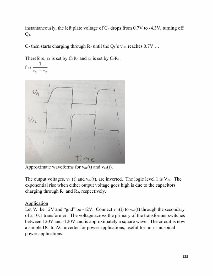
133
instantaneously, the left plate voltage of C2 drops from 0.7V to -4.3V, turning off Q1. C2 then starts charging through R2 until the Q1’s vBE reaches 0.7V … Therefore, τ1 is set by C1R3 and τ2 is set by C2R2.
f1
𝜏 𝜏
Approximate waveforms for vo1(t) and vo2(t). The output voltages, vo1(t) and vo2(t), are inverted. The logic level 1 is Vcc. The exponential rise when either output voltage goes high is due to the capacitors charging through R1 and R4, respectively. Application Let Vcc be 12V and “gnd” be -12V. Connect vo1(t) to vo2(t) through the secondary of a 10:1 transformer. The voltage across the primary of the transformer switches between 120V and -120V and is approximately a square wave. The circuit is now a simple DC to AC inverter for power applications, useful for non-sinusoidal power applications.