tsmc maintains a network of important external r&d · 2019-07-25 · tsmc maintains a network...
TRANSCRIPT

073072 073072 073

074 075
TSMC maintains a network of important external R&D partnerships and alliances with world-class research institutions, including GRC/SRC in the US, and IMEC the highly regarded European R&D consortium, where TSMC is a core partner. TSMC also provides funding for nanotechnology research at leading universities worldwide to promote innovation and the advancement of nano-electronic technology.
5.2.2 R&D Accomplishments in 2017
Highlights● �7nm Technology7nm technology offers significant performance, power and density improvement compared to previous technology generations. In 2017, TSMC successfully completed 7nm technology qualification for volume production, as major customers completed IP validation and started product tape-out. Ramp-up to volume production is expected in first half of 2018.
● �5nm TechnologyEven though the semiconductor industry is approaching the physical limits of silicon, 5nm technology still follows MooreÕ s Law and delivers substantial density improvement with better performance at same power or lower power consumption at comparable performance. Development activities of 5nm technology in 2017 were focused on test vehicle pilot run, baseline process development, yield ramp, and transistor performance enhancement. In 2018, TSMC will continue
5.2 Technology Leadership
5.2.1 R&D Organization and Investment
In 2017 TSMC continued to invest in research and development, with total R&D expenditures amounting to 8% of revenue, a level that equals or exceeds the R&D investment of many other leading high- tech companies.
TSMC recognizes that the technology challenge of continuing to extend MooreÕ s Law, the doubling of semiconductor computing power every two years, is becoming increasingly complex and difficult. The efforts of the R&D organization are focused on enabling the Company to continuously offer customers first-to-market, leading-edge technologies and design solutions that contribute to their product success in todayÕ s competitive environment. In 2017 the R&D organization met these challenges by completing the transfer to manufacturing of the industry leading 7nm technology, the fourth generation of technology platform to make use of 3D FinFET transistors. The R&D organization continues to fuel the pipeline of technological innovation needed to maintain industry leadership. TSMCÕ s 7nm technology is on track to ramp up volume production in 2018. TSMC 5nm technology continues in full development stage, and the definition and intensive early development efforts have been progressing for nodes beyond 5nm.
In addition to CMOS logic, TSMC conducts R&D on a wide range of other semiconductor technologies that provide the functionality required by customers for mobile SoC and other applications. Highlights in 2017 included: the high-volume production of Gen-2 Integrated Fan-Out Package on Package (InFO-PoP) for mobile application processor packaging; successful qualification of Gen-3 InFO-PoP advanced packaging technology for mobile applications and Integrated Fan-Out on Substrate (InFO-oS) for die-partition and HPC applications; 0.18µm third generation BCD (Bipolar-CMOS-DMOS) technology resulting in the leading performance quick charger and wireless charger in 2017; successful production launch of eFlash 40nm node, NOR-based cell technologies and Split-Gate cell for consumer electronics applications such as IoT, smartcards and micro controller units; development and manufacturing qualification of 650V, 100V E-HEMT, and RF 30V D-MISFET GaN devices; and 40nm high-voltage phase-2 technology readiness for both LCD and OLED drivers.
5.1.4 Production in 2017 and 2016
Wafers
Year Capacity Output Amount
2017 11-12 10-11 454,603
2016 10-11 9-10 405,462
Unit: Capacity / Output (million 12-inch equivalent wafers) / Amount (NT$ millions)
R&D Expenditures Amount: NT$ thousands
80,7
32,4
63
71,2
07,7
03
13,1
44,9
91
2016 2017 01/01/2018~ 02/28/2018
Operational Highlights5.
5.1 Business Activities
5.1.1 Business Scope
As the founder and leader of the dedicated semiconductor foundry segment, TSMC provides a full range of integrated semiconductor foundry services, including the most advanced process technologies, leading specialty technologies, the most comprehensive design ecosystem support, excellent manufacturing productivity and quality, advanced mask and packaging services, and so on, to meet a growing variety of customer needs. The Company strives to provide the best overall value to its customers and views customer success as TSMC success. As a result, TSMC has won customer trust from around the world and has experienced strong growth and success.
5.1.2 Customer Applications
TSMC manufactured 9,920 different products for 465 customers in 2017. These chips were used across a broad spectrum of electronic applications, including computers and peripherals, information appliances, wired and wireless communication systems, automotive and industrial equipment, consumer electronics such as digital TVs, game consoles, digital cameras and many other devices and applications.
The rapid ongoing evolution of end products prompts customers to pursue differentiation using TSMCÕ s innovative technologies and services and, at the same time, spurs TSMCÕ s own development of technology. As always, success depends on leading rather than following industry trends.
5.1.3 Consolidated Shipments and Net Revenue in 2017 and 2016Unit: Shipments (thousand 12-inch equivalent wafers) / Net Revenue (NT$ thousands)
2017 2016
Shipments Net Revenue Shipments Net Revenue
Wafer Domestic (Note 1) 1,650 89,796,998 1,849 127,717,686
Export 8,799 784,775,622 7,757 733,453,169
Others (Note 2) Domestic (Note 1) N/A 7,969,232 N/A 6,802,548
Export N/A 94,905,389 N/A 79,964,941
Total Domestic (Note 1) 1,650 97,766,230 1,849 134,520,234
Export 8,799 879,681,011 7,757 813,418,110
Note 1: Domestic means sales to Taiwan.Note 2: Others mainly include revenue associated with packaging and testing services, mask making, design services, and royalties.

076 077
transistor research in areas such as high mobility channel, novel gate stack materials, and device structures for reduced operating voltage and enhanced off state control. TSMC research is well positioned to pave the way for continued density scaling, performance enhancement and power reduction to deliver advanced logic technologies for mobile and high-performance applications.
Specialty TechnologiesTSMC offers a broad mix of technologies to address a wide range of applications:
● �Mixed Signal/Radio Frequency (MS/RF) TechnologyIn 2017, in order to facilitate circuit design for the increasing demand of 5G cutting-edge wireless technologies, TSMC successfully delivered 22nm devices with a Si-based millimeter-wave (mmWave) model to fulfill a customer’s request for transceiver design to support faster application. To achieve better performance in insertion loss and isolation, TSMC reduced the key parameter Ron-Coff to~85 fs (femtosecond) in 0.11µm process for cellar/Wi-Fi RF switch applications as a lower-cost alternative.
● �Power IC/Bipolar-CMOS-DMOS (BCD) TechnologyTSMC’s 0.18µm third-generation BCD technology went into production in 2017. The technology provides the world’s leading performance for fast charger, wireless charger and panel Power Management IC (PMIC). TSMC continually enriches this platform to cover more PMIC applications with 40nm eFlash compatible 7-30V HV (high voltage) devices for the first time to enable low power, high integration and small footprint in mobile applications. ● �Panel DriversIn 2017, TSMC completed 40nm high-voltage phase-2 technology qualification and transferred to fab. Several customers passed product qualification with good yield. This technology supports Super Retina display driver ICs in LCD, OLED and touch-display driver ICs for high-end mobile phones. For next generation HV panel display driver, TSMC plans to deliver high-speed, low active power 28HPC+ technology in both wafer-on-wafer stacking and high-voltage monolithic technologies.
● �Micro-electromechanical Systems (MEMS) TechnologyIn 2017, TSMC’s modular MEMS technology was qualified for mass production of accelerometers and a pilot run of high-resolution pressure sensors. Future plans include
the development of next-generation high-sensitivity thin microphone, MEMS Si-pillar TSV (through silicon via) technology and BioMEMS applications.
● �GaN TechnologyThe next generations of 650V/100V enhanced-high electron mobility transistor (E-HEMT) and RF 30V D-MISFET GaN devices were developed and qualified for manufacturing in 2017.
● �Complementary Metal-Oxide-Semiconductor (CMOS) Image Sensor Technology
In 2017, TSMC had several achievements in CMOS image sensor technology including: (1) high-performance sub-micron pixel development, which was completed and made ready for mass production; (2) quantum efficiency (QE), which gained significant boost on near-infrared sensors by innovated structure and usage of new material; and (3) pitch density of wafer bond technology, which was pushed higher to maintain the Company’s world-wide leading position.
● �Embedded Flash/Emerging Memory TechnologyTSMC achieved several major milestones in non-volatile memory (NVM) technologies in 2017. At the 40nm node, NOR-based cell technology with Split-Gate cell was successfully mass-produced to support consumer electronics applications such as IoT, smartcards and micro controller units (MCU). This technology will be incorporated in automobile electronics and mass production is expected in first half of 2018. Embedded flash development on the 28nm low-power and 28nm high-performance mobile computing platforms has demonstrated preliminary yield and reliability, and technical qualification is expected in 2019 for low-leakage applications in areas such as automobile electronics and micro controller units. TSMC is developing embedded resistive random access memory (RRAM) technology as a low-cost solution to split-gate technology, completing the 40nm technical qualification. With production expected in 2018, this technology will be mainly applied to the price sensitive IoT market. 22nm embedded resistive memory technology is also being developed. Compared to 40nm technology, 22nm embedded resistive memory unit cell area will be substantially scaled and expected to enter mass production in 2020. TSMC is also developing embedded MRAM (Magnetoresistive Random Access Memory) technology as embedded-flash technology replacement beyond 40nm node for many emerging applications.
5nm full development focusing on manufacturing baseline process setup, yield learning, transistor and interconnect R/C performance improvement and reliability evaluation, targeting risk production in 2019.
● �Lithography TechnologyThe main focus for R&D lithography in 2017 is 7nm technology transfer, 5nm technology development and preparation of 5nm beyond development. For 7nm development, the technology was smoothly transferred and R&D is working with the fab to clean up the remaining patterning issues. As for 5nm development, EUV (extreme ultraviolet) lithography showed promising imaging capability with expected good wafer yield. R&D is working on EUV cost reduction, mask defect reduction in scanner, and mask-making capability improvement. In 2018, TSMC will intensively focus on improving EUV quality and adopting more EUV layers in 5nm and beyond technology.
In 2017, the EUV program made continuous improvement in light-source power and its stability, which has enabled faster learning rate and process development for advanced nodes. Additional progress was made with resist process, pellicle, and related mask blanks, as EUV technology moves closer to full scale R&D and manufacturing readiness.
● �Mask TechnologyMask technology is an integral part of advanced lithography. In 2017, R&D successfully implemented EUV mask technology into 7nm and 5nm nodes. Solid progress was made on the production yield and the reduction of blank native defects to meet high-volume manufacturing requirements.
Integrated Interconnect and PackagingWafer Level System Integration (WLSI) is a disruptive technology that leverages TSMC’s core competency in wafer processes and capacity in building up heterogeneous system integration and packaging to meet specific customer needs in system-level performance, power, profile, cycle time and cost. WLSI and its associated technology platforms, including CoWoS®, InFO and Under-Bump-Metallurgy Free Integration (UFI), are continuously evolving to fulfill diversified customer needs in mobile computing, IoT, automotive, and high-performance computing.
● �3D IC and Si InterposerInterposer CoWoS® demand is growing rapidly in the high-performance computing (HPC) area, both in volume and the number of products. Typical CoWoS® applications involve
heterogeneous integration of a large logic chip at 16/12/7nm and a growing number of HBM2 (second generation high bandwidth memory) stacks. Consequently, the Si interposer area has grown very fast to an astonishing ~1400mm2 in some applications. TSMC continues to provide a complete Si-to-package business model for CoWoS® manufacturing.
● �Advanced Fan-Out Packaging In 2017, TSMC continued to lead in high-volume manufacturing (HVM) of InFO-PoP Gen-2 packaging for mobile applications processors. During the year, the Company also successfully qualified InFO-PoP Gen-3 advanced packaging technology for mobile applications and started risk production in Integrated Fan-Out on Substrate (InFO-oS) for HPC die-partition application. The newly developed InFO-PoP could be stacked with versatile commercial DRAM with competitive performance. This InFO-PoP with backside RDL will boost penetration into mobile application processor application with wide coverage from premium to mid and low tiers. TSMC has scheduled HVM readiness by end of 2018. To meet demand with the coming of 5G mobile communications, TSMC has developed an advanced InFO antenna in package (InFO-AIP) technology, in which the RF chip and millimeter-wave antenna are integrated into an InFO package. InFO-AIP technology provides high-performance, low-power, small-size, low-cost solutions for millimeter wave system applications such as 5G mobile, video streaming and virtual reality (VR) wireless communications. This technology can also support the fast-evolving applications in car radar, auto-driving and driving safety.
● �Advanced InterconnectTSMC has made significant progress in innovative materials and processes for continuous interconnect scaling. The Company has developed and verified a novel low-k process using selective deposition on dielectric, which can lower capacitance loading, improve electric performance and enhance device reliability. In addition, TSMC has developed a new barrier and copper gap filling process to further extend copper material applications and provide competitive wire conductance and via resistance for advanced technology nodes. Verification of these new materials and processes is progressing well for beyond 5nm technologies.
Advanced Transistor ResearchInnovation in transistor architectures and materials continues to enable higher speed and reduced power consumption in advanced logic technologies. TSMC is at the forefront of
078 079
5.2.3 Technology Platform
TSMC provides customers with advanced technology platforms that include the comprehensive design infrastructure required to optimize design productivity and cycle time. These include: design flows for electronic design automation (EDA); silicon-proven IP building blocks, such as libraries; and simulation and verification design kits, i.e., process design kits (PDKs) and technology files.
For TSMC’s latest advanced technologies of 7nm, 12nm and 3D IC design enablement platform, EDA tools, features and IP solutions are readily available for customers to adopt to meet their product requirements at various design stages. TSMC also extended its IP quality program (TSMC 9000) to allow IP audits to be performed either at TSMC or at TSMC-certified laboratories. To help customers plan new product tape-outs incorporating IP/Library from TSMC’s Open Innovation Platform® (OIP) ecosystem, the OIP ecosystem added a portal to connect customers to an ecosystem of 40 solution providers. Overall, TSMC and its IP partners have accumulated a portfolio of 16,000 IP titles, from 0.35µm-7nm with major IP types to meet customer design needs. TSMC and its EDA partners have created numerous deliverables from 0.13µm-7nm that have successfully supported customer tape-outs.
5.2.4 Design Enablement
TSMC’s technology platforms provide a solid foundation to facilitate the design process. Customers can design directly using the Company’s internally developed IP and tools or using those that are available from TSMC’s OIP partners.
Tech Files and PDKsEDA tool certification is an essential foundation for IP and customer designs to ensure that the features meet TSMC process technology requirements, with certification results that can be found on TSMC-Online. There are corresponding technology files and process development kits (PDKs) available for customers to download and design together with certified EDA tools. TSMC provides a broad range of PDKs for digital logic, mixed-signal, radio frequency (RF), high-voltage driver, CMOS image sensor (CIS) and embedded flash technologies across a range of technology nodes from 0.5µm to 7nm. In addition, the Company provides technology files for design rule checking (DRC), layout verification of schematic (LVS), resistance-capacitance (RC) extraction, automatic place and route, and a layout editor to ensure process technology
information is accurately represented in electronic design automation tools. By 2017, TSMC had provided more than 9,000 technology files and more than 300 PDKs via TSMC-Online. There are more than 100,000 customer downloads of these files every year.
Library and IPSilicon Intellectual property (IP) is the basic building block of integrated circuit designs. Various IP types are available to support different customer design applications including foundation IP, analog IP, embedded memory IP, interface IP and soft IP. TSMC and its alliance partners offer customers a rich portfolio of reusable IPs, which are essential building blocks for many circuit designs. In 2017, the Company expanded its library and silicon IP portfolio to contain more than 16,000 items, a 33% increase over 2016.
Design Methodology and FlowReference flows are built on top of certified EDA (Electronic Design Automation) tools to provide additional design flow methodology innovations that can help boost productivity. In 2017, TSMC addressed critical design challenges associated with the new 7nm+, 12nm FinFET and 3DIC technology for digital and SoC applications by announcing the readiness of reference flows through OIP collaboration that feature FinFET-specific design solutions and methodologies for performance, power and area optimization.
5.2.5 Intellectual Property
A strong portfolio of intellectual property rights strengthens TSMC’s technology leadership and protects our advanced and leading-edge technologies. As of end of 2017, TSMC has accumulated over 40,000 patent applications, and over 30,000 patent grants worldwide. In 2017, TSMC has obtained 2,428 U.S. patents to rank #9 among U.S. patent assignees, making the ranking of top 10 U.S. patent assignees for the second consecutive year. Additionally, TSMC actively develops worldwide patent strategy, ranking #1 among patent applicants in Taiwan, and obtaining over 1,100 patents in Taiwan and China. In terms of patent quality, the average allowance rate of TSMC’s U.S. applications is 98% and ranks #1 among top 10 U.S. patent assignees. Going forward, TSMC will continue to implement a unified strategic plan for intellectual capital management, combining with strategic considerations and close alignment with the business objectives, to drive the timely creation, management and use of intellectual property.
TSMC has established a process to generate company value from intellectual property by aligning intellectual property strategy with R&D, business operation objectives, marketing, and corporate development strategies. Intellectual property rights protect the company’s freedom to operate, enhance competitive position, and provide leverage to participate in many profit-generating activities.
TSMC has worked continuously to improve the quality of intellectual property portfolio and to reduce the maintenance costs. TSMC will continue to invest in intellectual property portfolio and intellectual property management system to ensure the company’s technology leadership and receive maximum business value from intellectual property rights.
5.2.6 TSMC University Collaboration Programs
In recent years TSMC has significantly expanded its collaboration on research projects at some of Taiwan’s most prestigious universities. The mission of these projects is twofold: to increase the number of highly qualified students suitable for employment in the semiconductor industry, and to inspire university professors to initiate research programs that focus on the frontiers of semiconductor science, including device, process and materials technology, semiconductor manufacturing and engineering science, and specialty technologies for electronic applications. In the past five years, TSMC has established research centers at four institutions: National Chiao Tung University, National Taiwan University, National Cheng Kung University and National Tsing Hua University. In 2015, TSMC started collaborating with the International College of Semiconductor Technology, National Chiao Tung University and continued to enhance cooperation with other schools. Currently, several hundred high-caliber students have joined the research centers with backgrounds in the disciplines of electronics, physics, materials, chemistry, chemical engineering and mechanical engineering.
In addition, TSMC also conducts strategic research projects at top overseas universities, such as Stanford, MIT, UC Berkeley and so on. The focus is on disruptive capabilities in transistors, interconnect, patterning, modeling and special technologies.
TSMC University Shuttle ProgramThe TSMC University Shuttle Program was established to provide professors at leading research universities worldwide with access to the advanced silicon process technologies
needed to research and develop innovative circuit design concepts. This program links motivated professors and graduate students with enthusiastic managers at TSMC in order to promote excellence in the development of advanced silicon design technologies and nurture new generations of engineering talent in the semiconductor field.
The program provides access to TSMC silicon process technologies for digital and analog/mixed-signal circuits, RF designs and micro-electromechanical system designs. Participants include major university research groups worldwide. TSMC and the University Shuttle Program participants achieve “win-win” collaboration through the program, which allows graduate students to implement exciting designs and achieve silicon proof points for innovations in various end-applications.
5.2.7 Future R&D Plans
To maintain and strengthen TSMC’s technology leadership, the Company plans to continue investing heavily in R&D. For advanced CMOS logic, the Company’s 7nm and 5nm CMOS nodes continue progressing in the pipeline. In addition, the Company’s reinforced exploratory R&D work is focused on beyond-5nm node; in areas such as 3D transistors, new memory, and low-R interconnect, on track to establish a solid foundation to feed into technology platforms. For 3D IC advanced packaging, innovations for energy-efficient sub-system integration and scaling provide further augmentation to CMOS logic applications. For specialty technologies, the Company has intensified focus on new specialty technologies such as RF and 3D intelligent sensors targeting 5G and smart IoT applications. In 2017, a new Corporate Research function is established to focus on novel materials, process, devices, nanowires, memories, and etc. for long term horizon which is beyond 8-10 years. The Company also continues to collaborate with external research bodies from academia to industry consortia alike with the goal of extending Moore’s Law and paving the road to future cost-effective technologies and manufacturing solutions for its customers.
With a highly competent and dedicated R&D team and its unwavering commitment to innovation, TSMC is confident in its ability to deliver the best and most cost-effective SoC technologies to its customers and to drive future business growth and profitability for years to come.
080 081
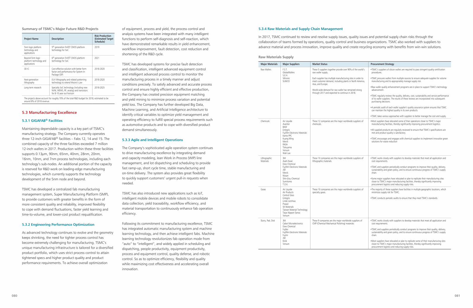
Summary of TSMC’s Major Future R&D Projects
Project Name DescriptionRisk Production (Estimated Target Schedule)
5nm logic platform technology and applications
5th generation FinFET CMOS platform technology for SoC
2019
Beyond-5nm logic platform technology and applications
6th generation FinFET CMOS platform technology for SoC
2021
3D IC Cost-effective solution with better form factor and performance for System-in-Package (SiP)
2018-2020
Next-generation lithography
EUV lithography and related patterning technology to extend Moore’s Law
2018-2020
Long-term research Specialty SoC technology (including new NVM, MEMS, RF, analog) and transistors for 8-10 year out horizon
2018-2025
The projects above account for roughly 70% of the total R&D budget for 2018, estimated to be around 8% of 2018 revenue.
5.3 Manufacturing Excellence
5.3.1 GIGAFAB® Facilities
Maintaining dependable capacity is a key part of TSMC’s manufacturing strategy. The Company currently operates three 12-inch GIGAFAB® facilities – Fabs 12, 14 and 15. The combined capacity of the three facilities exceeded 7 million 12-inch wafers in 2017. Production within these three facilities supports 0.13µm, 90nm, 65nm, 40nm, 28nm, 20nm, 16nm, 10nm, and 7nm process technologies, including each technology’s sub-nodes. An additional portion of the capacity is reserved for R&D work on leading-edge manufacturing technologies, which currently supports the technology development of the 5nm node and beyond.
TSMC has developed a centralized fab manufacturing management system, Super Manufacturing Platform (SMP), to provide customers with greater benefits in the form of more consistent quality and reliability, improved flexibility to cope with demand fluctuations, faster yield learning and time-to-volume, and lower-cost product requalification.
5.3.2 Engineering Performance Optimization
As advanced technology continues to evolve and the geometry keeps shrinking, the need for tighter process control has become extremely challenging for manufacturing. TSMC’s unique manufacturing infrastructure is tailored for a diversified product portfolio, which uses strict process control to attain tightened specs and higher product quality and product performance requirements. To achieve overall optimization
5.3.4 Raw Materials and Supply Chain Management
In 2017, TSMC continued to review and resolve supply issues, quality issues and potential supply chain risks through the collaboration of teams formed by operations, quality control and business organizations. TSMC also worked with suppliers to advance material and process innovation, improve quality and create recycling economy with benefits from win-win solutions.
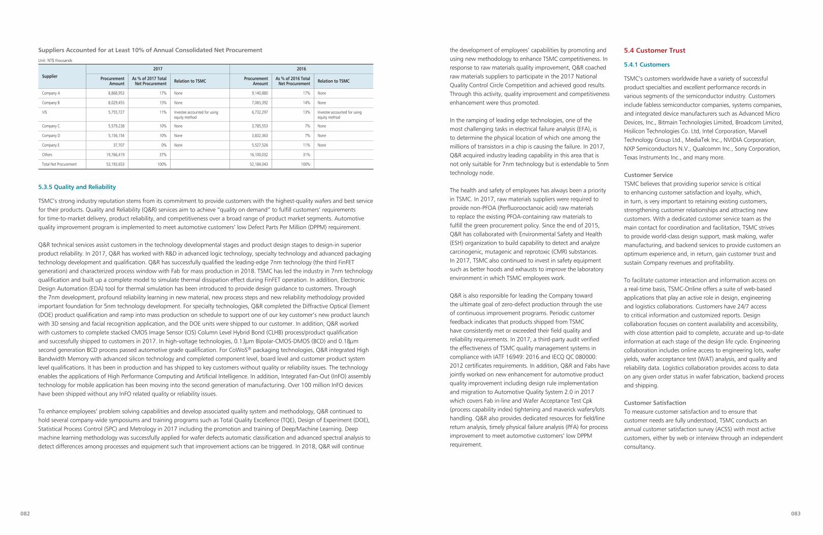
Raw Materials Supply
Major Materials Major Suppliers Market Status Procurement Strategy
Raw Wafers F.S.T. GlobalWafersS.E.H.SiltronicSUMCO
These 5 suppliers together provide over 90% of the world’s raw wafer supply.
Each supplier has multiple manufacturing sites in order to meet customer demand, including plants in North America, Asia, and Europe.
World-wide demand for raw wafer has remained strong through 2017 and expected to continue in 2018.
● �TSMC’s suppliers of silicon wafers are required to pass stringent quality certification procedures.
● �TSMC procures wafers from multiple sources to ensure adequate supplies for volume manufacturing and to appropriately manage supply risk.
● �Raw wafer quality enhancement programs are in place to support TSMC’s technology advancement.
● �TSMC regularly reviews the quality, delivery, cost, sustainability and service performance of its wafer suppliers. The results of these reviews are incorporated into subsequent purchasing decisions.
● �A periodic audit of each wafer supplier’s quality assurance system ensures that TSMC can maintain the highest quality in its own products.
● �TSMC takes various approaches with suppliers to better manage the cost and supply.
Chemicals Air LiquideAvantorBASFEntegrisFujifilm Electronic MaterialsKanto PPC Kuang MingMerckRASA TokuyamaVersumWah Lee
These 12 companies are the major worldwide suppliers of chemicals.
● �Most suppliers have relocated some of their operations closer to TSMC’s major manufacturing facilities, thereby significantly improving procurement logistics.
● �All supplied products are regularly reviewed to ensure that TSMC’s specifications are met and product quality is satisfactory.
● �TSMC encourages and engages with chemical suppliers to implement innovative green solutions for waste reduction
Lithographic Materials
3MAsahi KaseiDow ChemicalFujifilm Electronic MaterialsJSRMerckNissanShin-Etsu ChemicalSumitomoT.O.K.
These 10 companies are the major worldwide suppliers of lithographic materials.
● �TSMC works closely with suppliers to develop materials that meet all application and cost requirements.
● �TSMC and suppliers periodically conduct programs to improve their quality, delivery, sustainability and green policy, and to ensure continuous progress of TSMC’s supply chain.
● �Some major suppliers have relocated or plan to replicate their manufacturing sites closer to TSMC’s major manufacturing facilities, thereby significantly improving procurement logistics and reducing supply risks.
Gases Air LiquideAir ProductsCentral GlassEntegrisLinde LienHwaPraxairSK MaterialsTaiwan Material TechnologyTaiyo Nippon SansoVersum
These 10 companies are the major worldwide suppliers of specialty gases.
● �The majority of these suppliers have facilities in multiple geographic locations, which minimizes supply risk for TSMC.
● �TSMC conducts periodic audits to ensure that they meet TSMC’s standards.
Slurry, Pad, Disk 3MCabot MicroelectronicsDow ChemicalFujiboFujifilm Electronic MaterialsFujimiJSRKinikVersum
These 9 companies are the major worldwide suppliers of CMP (Chemical Mechanical Polishing) materials.
● �TSMC works closely with suppliers to develop materials that meet all application and cost requirements.
● �TSMC and suppliers periodically conduct programs to improve their quality, delivery, sustainability and green policy, and to ensure continuous progress of TSMC’s supply chain.
● �Most suppliers have relocated or plan to replicate some of their manufacturing sites closer to TSMC’s major manufacturing facilities, thereby significantly improving procurement logistics and reducing supply risks.
of equipment, process and yield, the process control and analysis systems have been integrated with many intelligent functions to perform self-diagnosis and self-reaction, which have demonstrated remarkable results in yield enhancement, workflow improvement, fault detection, cost reduction and shortening of the R&D cycle.
TSMC has developed systems for precise fault detection and classification, intelligent advanced equipment control and intelligent advanced process control to monitor the manufacturing process in a timely manner and adjust conditions precisely. To satisfy advanced and accurate process control and ensure highly efficient and effective production, the Company has created precision equipment matching and yield mining to minimize process variation and potential yield loss. The Company has further developed Big Data, Machine Learning, and Artificial Intelligence architecture to identify critical variables to optimize yield management and operating efficiency to fulfill special process requirements such as automotive products and to cope with diversified product demand simultaneously.
5.3.3 Agile and Intelligent Operations
The Company’s sophisticated agile operation system continues to drive manufacturing excellence by integrating demand and capacity modeling, lean Work in Process (WIP) line management, and lot dispatching and scheduling to provide fast ramp-up, short cycle time, stable manufacturing and on-time delivery. The system also provides great flexibility to quickly support customers’ urgent pull-in requests when needed.
TSMC has also introduced new applications such as IoT, intelligent mobile devices and mobile robots to consolidate data collection, yield traceability, workflow efficiency, and material transportation to continuously enhance fab operation efficiency.
Following its commitment to manufacturing excellence, TSMC has integrated automatic manufacturing system and machine learning technology, and then achieve intelligent fabs. Machine learning technology revolutionizes fab operation mode from “auto” to “intelligent”, and widely applied in scheduling and dispatching, people productivity, equipment productivity, process and equipment control, quality defense, and robotic control. So as to optimize efficiency, flexibility and quality while maximizing cost effectiveness and accelerating overall innovation.
082 083
5.3.5 Quality and Reliability
TSMC’s strong industry reputation stems from its commitment to provide customers with the highest-quality wafers and best service for their products. Quality and Reliability (Q&R) services aim to achieve “quality on demand” to fulfill customers’ requirements for time-to-market delivery, product reliability, and competitiveness over a broad range of product market segments. Automotive quality improvement program is implemented to meet automotive customers’ low Defect Parts Per Million (DPPM) requirement.
Q&R technical services assist customers in the technology developmental stages and product design stages to design-in superior product reliability. In 2017, Q&R has worked with R&D in advanced logic technology, specialty technology and advanced packaging technology development and qualification. Q&R has successfully qualified the leading-edge 7nm technology (the third FinFET generation) and characterized process window with Fab for mass production in 2018. TSMC has led the industry in 7nm technology qualification and built up a complete model to simulate thermal dissipation effect during FinFET operation. In addition, Electronic Design Automation (EDA) tool for thermal simulation has been introduced to provide design guidance to customers. Through the 7nm development, profound reliability learning in new material, new process steps and new reliability methodology provided important foundation for 5nm technology development. For specialty technologies, Q&R completed the Diffractive Optical Element (DOE) product qualification and ramp into mass production on schedule to support one of our key customer’s new product launch with 3D sensing and facial recognition application, and the DOE units were shipped to our customer. In addition, Q&R worked with customers to complete stacked CMOS Image Sensor (CIS) Column Level Hybrid Bond (CLHB) process/product qualification and successfully shipped to customers in 2017. In high-voltage technologies, 0.13µm Bipolar-CMOS-DMOS (BCD) and 0.18µm second generation BCD process passed automotive grade qualification. For CoWoS® packaging technologies, Q&R integrated High Bandwidth Memory with advanced silicon technology and completed component level, board level and customer product system level qualifications. It has been in production and has shipped to key customers without quality or reliability issues. The technology enables the applications of High Performance Computing and Artificial Intelligence. In addition, Integrated Fan-Out (InFO) assembly technology for mobile application has been moving into the second generation of manufacturing. Over 100 million InFO devices have been shipped without any InFO related quality or reliability issues.
To enhance employees’ problem solving capabilities and develop associated quality system and methodology, Q&R continued to hold several company-wide symposiums and training programs such as Total Quality Excellence (TQE), Design of Experiment (DOE), Statistical Process Control (SPC) and Metrology in 2017 including the promotion and training of Deep/Machine Learning. Deep machine learning methodology was successfully applied for wafer defects automatic classification and advanced spectral analysis to detect differences among processes and equipment such that improvement actions can be triggered. In 2018, Q&R will continue
the development of employees’ capabilities by promoting and using new methodology to enhance TSMC competitiveness. In response to raw materials quality improvement, Q&R coached raw materials suppliers to participate in the 2017 National Quality Control Circle Competition and achieved good results. Through this activity, quality improvement and competitiveness enhancement were thus promoted.
In the ramping of leading edge technologies, one of the most challenging tasks in electrical failure analysis (EFA), is to determine the physical location of which one among the millions of transistors in a chip is causing the failure. In 2017, Q&R acquired industry leading capability in this area that is not only suitable for 7nm technology but is extendable to 5nm technology node.
The health and safety of employees has always been a priority in TSMC. In 2017, raw materials suppliers were required to provide non-PFOA (Perfluorooctanoic acid) raw materials to replace the existing PFOA-containing raw materials to fulfill the green procurement policy. Since the end of 2015, Q&R has collaborated with Environmental Safety and Health (ESH) organization to build capability to detect and analyze carcinogenic, mutagenic and reprotoxic (CMR) substances. In 2017, TSMC also continued to invest in safety equipment such as better hoods and exhausts to improve the laboratory environment in which TSMC employees work.
Q&R is also responsible for leading the Company toward the ultimate goal of zero-defect production through the use of continuous improvement programs. Periodic customer feedback indicates that products shipped from TSMC have consistently met or exceeded their field quality and reliability requirements. In 2017, a third-party audit verified the effectiveness of TSMC quality management systems in compliance with IATF 16949: 2016 and IECQ QC 080000: 2012 certificates requirements. In addition, Q&R and Fabs have jointly worked on new enhancement for automotive product quality improvement including design rule implementation and migration to Automotive Quality System 2.0 in 2017 which covers Fab in-line and Wafer Acceptance Test Cpk (process capability index) tightening and maverick wafers/lots handling. Q&R also provides dedicated resources for field/line return analysis, timely physical failure analysis (PFA) for process improvement to meet automotive customers’ low DPPM requirement.
Supplier
2017 2016
Procurement Amount
As % of 2017 Total Net Procurement Relation to TSMC Procurement
Amount As % of 2016 Total
Net Procurement Relation to TSMC
Company A 8,868,953 17% None 9,140,880 17% None
Company B 8,029,455 15% None 7,065,392 14% None
VIS 5,755,727 11% Investee accounted for using equity method
6,732,297 13% Investee accounted for using equity method
Company C 5,579,238 10% None 3,785,553 7% None
Company D 5,156,154 10% None 3,832,363 7% None
Company E 37,707 0% None 5,527,526 11% None
Others 19,766,419 37% 16,100,032 31%
Total Net Procurement 53,193,653 100% 52,184,043 100%
Unit: NT$ thousands
Suppliers Accounted for at Least 10% of Annual Consolidated Net Procurement 5.4 Customer Trust
5.4.1 Customers
TSMC’s customers worldwide have a variety of successful product specialties and excellent performance records in various segments of the semiconductor industry. Customers include fabless semiconductor companies, systems companies, and integrated device manufacturers such as Advanced Micro Devices, Inc., Bitmain Technologies Limited, Broadcom Limited, Hisilicon Technologies Co. Ltd, Intel Corporation, Marvell Technology Group Ltd., MediaTek Inc., NVIDIA Corporation, NXP Semiconductors N.V., Qualcomm Inc., Sony Corporation, Texas Instruments Inc., and many more.
Customer ServiceTSMC believes that providing superior service is critical to enhancing customer satisfaction and loyalty, which, in turn, is very important to retaining existing customers, strengthening customer relationships and attracting new customers. With a dedicated customer service team as the main contact for coordination and facilitation, TSMC strives to provide world-class design support, mask making, wafer manufacturing, and backend services to provide customers an optimum experience and, in return, gain customer trust and sustain Company revenues and profitability.
To facilitate customer interaction and information access on a real-time basis, TSMC-Online offers a suite of web-based applications that play an active role in design, engineering and logistics collaborations. Customers have 24/7 access to critical information and customized reports. Design collaboration focuses on content availability and accessibility, with close attention paid to complete, accurate and up-to-date information at each stage of the design life cycle. Engineering collaboration includes online access to engineering lots, wafer yields, wafer acceptance test (WAT) analysis, and quality and reliability data. Logistics collaboration provides access to data on any given order status in wafer fabrication, backend process and shipping.
Customer SatisfactionTo measure customer satisfaction and to ensure that customer needs are fully understood, TSMC conducts an annual customer satisfaction survey (ACSS) with most active customers, either by web or interview through an independent consultancy.
084 085
5.4.2 Open Innovation Platform® (OIP) Initiative
Innovation has always been an exciting and challenging proposition. Competition among semiconductor companies continues to grow more intense in the face of increasing customer consolidation and the commoditization of technology at more mature, conventional levels. Companies must find ways to keep innovating in order to survive and prosper. One way to accelerate innovation is through active collaboration with external partners. At TSMC this is known as the “Open Innovation® approach” and it is an “outside in” approach to complement traditional “inside out” methods. TSMC has adopted this path to innovate via its Open Innovation Platform® initiative, which is a key part of the TSMC Grand Alliance.
The OIP initiative is a comprehensive design technology infrastructure that encompasses all critical IC implementation areas to reduce design barriers and improve first-time silicon success. OIP promotes the speedy implementation of innovation amongst the semiconductor design community and its ecosystem partners using TSMC’s IP, design implementation and design for manufacturability (DFM) capabilities, process technology and backend services.
Crucial to OIP are ecosystem interfaces and collaborative components initiated and supported by TSMC that more efficiently empower innovation throughout the supply chain and, in turn, drive the creation and sharing of new revenue and profits. TSMC’s active accuracy assurance (AAA) initiative is key to OIP, providing the accuracy and quality required by the ecosystem interfaces and collaborative components.
TSMC’s Open Innovation® model brings together the creative thinking of customers and partners under the common goal of shortening each of the following: design time, time-to-volume, time-to-market and, ultimately, time-to-revenue. The model features:● �the foundry segment’s earliest and most comprehensive electronic design automation certification program, delivering timely
design tool enhancement required by new process technologies;
● �the foundry segment’s largest, most comprehensive and robust silicon-proven IP (intellectual properties) and library portfolio; and
● �comprehensive design ecosystem alliance programs covering market-leading EDA, library, IPs, and design service partners.
TSMC’s OIP alliance consists of 21 EDA partners, 40 IP partners, and 23 design service partners. TSMC and its partners work together proactively and engage much earlier and deeper than before in order to address mounting design challenges at advanced technology nodes. Through this early and intensive collaboration effort, TSMC’s OIP is able to deliver the needed design infrastructure with timely enhancement of EDA tools, early availability of critical IPs and quality design services when customers need them. Taking full advantage of the process technologies once they reach production-ready maturity is critical to customers’ success.
TSMC’s OIP partner management portal facilitates communication with our ecosystem partners for efficient business productivity. Designed with a highly intuitive interface, this portal can be accessed via a direct link from TSMC-Online.
TSMC held its 2017 Open Innovation Platform® Ecosystem Forum in September in Santa Clara, California with over 1,300 attendees. The annual event demonstrates how TSMC and our ecosystem partners jointly develop design solutions on top of TSMC’s advanced technologies through OIP collaboration. TSMC executive delivered key messages to help customer products’ time-to-market. TSMC has expanded design ecosystem solutions to address market demands with four application specific design platforms consisting of Mobile, High Performance Computing (HPC), Internet of Things and Automotive. In addition, TSMC continues to enhance 3DIC solutions to integrate high bandwidth memory (HBM) on integrated fan-out design flow to meet customers’ system integration and high memory bandwidth requirements. Furthermore, machine learning is being leveraged to enhance customers’ design power, performance and area (PPA) and productivity.
5.5 Human Capital
Human capital is TSMC’s most treasured asset. In this regard, the Company’s main role is to provide jobs with challenging, meaningful work in a safe environment with excellent compensation and benefits. TSMC goes beyond this, however,
by actively encouraging employees to nurture and enjoy a healthy family life, to develop outside interests, to expand social participation, and, in general, live a happy life.
TSMC believes that all employees, including contractors, and interns, should be treated with dignity and respect. Reflecting this commitment to employees, the Company has implemented a “TSMC Human Rights Policy,” which is based on “the International Bill of Human Rights,” “The International Labour Organization’s (ILO) Declaration on Fundamental Principles and Rights at Work” and “The United Nations Global Compact’s Ten Principles,” and adopts Responsible Business Alliance (RBA) Code of Conduct.
TSMC participates in the Responsible Business Alliance, RBA as a full member; the Company refrains from forcing employees to do unwilling labor service, listens to the employees, keeps communication channels open, respects employees’ right to form a labor union, and does not in any way impede employees’ freedom of association.
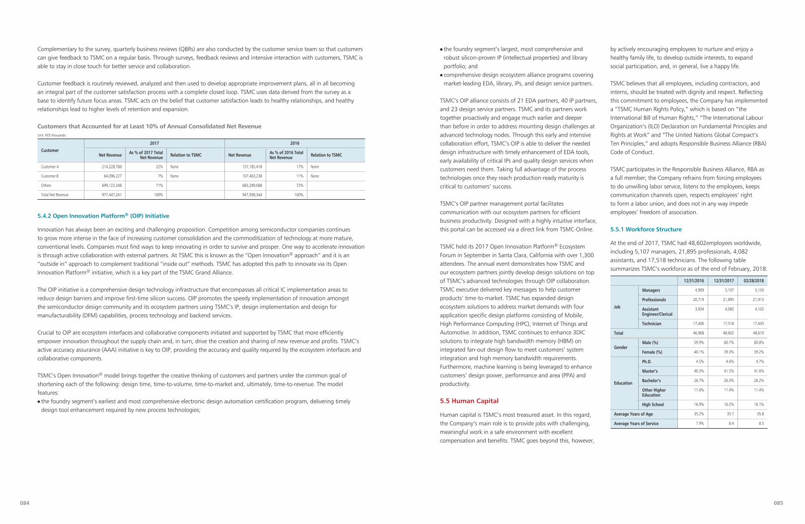
5.5.1 Workforce Structure
At the end of 2017, TSMC had 48,602employees worldwide, including 5,107 managers, 21,895 professionals, 4,082 assistants, and 17,518 technicians. The following table summarizes TSMC’s workforce as of the end of February, 2018:
12/31/2016 12/31/2017 02/28/2018
Job
Managers 4,909 5,107 5,150
Professionals 20,719 21,895 21,913
Assistant Engineer/Clerical
3,934 4,082 4,102
Technician 17,406 17,518 17,445
Total 46,968 48,602 48,610
GenderMale (%) 59.9% 60.7% 60.8%
Female (%) 40.1% 39.3% 39.2%
Education
Ph.D. 4.5% 4.6% 4.7%
Master’s 40.3% 41.5% 41.6%
Bachelor’s 26.7% 26.3% 26.2%
Other Higher Education
11.6% 11.4% 11.4%
High School 16.9% 16.2% 16.1%
Average Years of Age 35.2% 35.7 35.8
Average Years of Service 7.9% 8.4 8.5
Complementary to the survey, quarterly business reviews (QBRs) are also conducted by the customer service team so that customers can give feedback to TSMC on a regular basis. Through surveys, feedback reviews and intensive interaction with customers, TSMC is able to stay in close touch for better service and collaboration.
Customer feedback is routinely reviewed, analyzed and then used to develop appropriate improvement plans, all in all becoming an integral part of the customer satisfaction process with a complete closed loop. TSMC uses data derived from the survey as a base to identify future focus areas. TSMC acts on the belief that customer satisfaction leads to healthy relationships, and healthy relationships lead to higher levels of retention and expansion.
Customers that Accounted for at Least 10% of Annual Consolidated Net RevenueUnit: NT$ thousands
Customer
2017 2016
Net Revenue As % of 2017 Total Net Revenue Relation to TSMC Net Revenue As % of 2016 Total
Net Revenue Relation to TSMC
Customer A 214,228,766 22% None 157,185,418 17% None
Customer B 64,096,227 7% None 107,463,238 11% None
Others 699,122,248 71% 683,289,688 72%
Total Net Revenue 977,447,241 100% 947,938,344 100%

086 087
5.5.2 Recruitment
The key elements of TSMC’s success and growth depend on our employee who shares common goals and interests. In order to strengthen growth momentum, the Company is dedicated to recruiting top-notch professionals for all positions available. TSMC is an equal opportunity employer and operates on the principles of open and fair recruitment. The hiring principals are integrity and ability, and the Company evaluates all candidates according to their qualifications as related to the requirement of each position without regard to race, gender, age, religion, nationality or political affiliation. TSMC’s continuous growth requires constant talent sourcing and recruitment activities to support its business. The Company recruited more than 3,600 employees in 2017, including over 2,500 managers and professionals, as well as over 1,000 assistants and technicians.
5.5.3 People Development
Employee development is an integral and critical factor for the growth of any company and should be goal oriented, disciplined and planned. TSMC is committed to stretching employees’ potential by providing challenging work, global workplace and internal rotation opportunities. TSMC also committed to cultivating a consistent and diverse learning environment. To this end, the Company has initiated the “TSMC Employee Training and Education Procedure” to ensure the Company’s and the individuals’ development objectives can be achieved through the integration of internal and external training resources.
In order to actively develop talent and create a high-performance work environment, TSMC integrates internal and external resources and designs diversified development programs based on business objectives, the nature of the individual’s job, work performance and career development path. The Company provides employees a diverse network of learning resources, including on-the-job training, classroom training, e-learning, coaching, mentoring and job rotation; it also creates an educational atmosphere through learning activities in response to organization development requirements and employee capability enhancement goals.
The Company provides employees with a wide range of onsite general, professional and management training programs. In addition to engaging external experts as trainers, hundreds of TSMC employees are trained to be qualified instructors to deliver their valuable knowhow in internal training courses.
TSMC’s training programs include:● �New employee – for basic training and job orientation.
In addition, newcomers’ managers and the Company’s well-established buddy system are in place to support new hires in their assimilation process in both corporate culture and work requirements.
● �General – refers to training required by government regulations and/or Company policies, as well as training on general subjects for all employees or employees of different job functions. Topics include industry-specific safety, workplace health and safety, quality, fab emergency response and personal effectiveness.
● �Professional/functional – technical and professional training required by different functions within the Company. TSMC offers training courses on equipment engineering, process engineering, accounting, information technology, and so forth.
● �Management – management development programs tailored to the needs of managers at all levels based on their managerial capabilities and responsibilities, including new, experienced, and senior managers; optional courses are also available.
● �Direct labor – training for production-line employees to acquire the knowledge, skills and approaches they need to perform their jobs well and to pass certification for operating equipment. Includes direct labor skill training, technician “Train the Trainer” training, and manufacturing leader training.
● �Customized – programs tailored to the needs of the organization and/or the employee’s development plan.
In 2017, TSMC conducted 973 internal training sessions, which translated to a companywide total of 627,063 training hours with the participation of 539,334 attendees. Employees on average attended over 13 hours of training with total training expenses reaching NT$63,277,222.
Apart from internal training resources, our employees are also subsidized when pursuing external short-term courses, for-credit courses and degrees.
5.5.4 Compensation
Employment at TSMC entitles employees to a comprehensive compensation and benefits program above the industry average. TSMC provides a diversified compensation program that is competitive externally, fair internally, and adapted locally. TSMC adheres to the philosophy of sharing wealth with employees in order to attract, retain, develop, motivate and reward talented employees. With sound business results for the past 30 years, the actual total compensation received by employees has also been above the industry’s average.
TSMC’s compensation program includes a monthly salary, employee cash bonuses based on quarterly business results, and an employee profit sharing bonus based on annual profits.
The purpose of the employee cash bonus and profit sharing bonus programs is to reward employee contributions appropriately, to encourage employees to work consistently toward ensuring the success of TSMC, and to align employees’ interests with those of TSMC’s shareholders so as to achieve win-win among the Company, shareholders and employees. The Company determines the amount of the cash bonus and profit sharing bonus based on operating results and industry practice in the Republic of China. The amount and distribution approach of the employee cash bonus and profit sharing bonus are recommended by the Compensation Committee to the Board of Directors for approval. Individual rewards are based on each employee’s job responsibility, contribution and performance.
The same philosophy applies to TSMC’s compensation programs of overseas subsidiaries. In addition to providing employees of TSMC’s overseas subsidiaries with a locally competitive base salary, the Company grants annual bonuses as a part of total compensation. The annual bonuses are granted in line with local regulations, market practices, and the overall operating performance of each subsidiary, to encourage employee commitment and development with the Company.
5.5.5 Employee Engagement
The Company encourages employees to maintain a healthy and well-balanced life while pursuing their goals effectively. TSMC continuously facilitate employee communication, and provide employee caring, benefit, rewards and recognition programs, including:
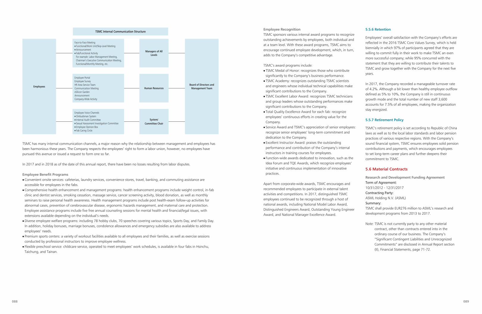
Employee CommunicationTSMC values two-way communication and is committed to keeping communication channels open and transparent for the management, subordinates and peers. To ensure that employees’ opinions and voices are heard and their issues are addressed effectively, impartial submission mechanisms, including quarterly labor-management communication meetings, are in place to provide fair and timely support. TSMC makes continuous efforts to facilitate mutual and timely employee communication, based on multiple channels and platforms, which in turn fosters harmonious labor relations and creates a win-win situation for the Company and employees.
A host of two-way communication channels are constructed to maintain the free flow of information between managers and employees, including:● �Communication meetings for various levels of managers and
employees.● �Periodic employee satisfaction surveys, with follow-up actions
based on the survey findings.● �The employee portal, myTSMC, an internal website featuring
the Chairman’s talk, corporate messages, executive interviews, and other activities of interest to employees.
● �eSilicon Garden, a website hosting TSMC’s internal electronic publications providing real-time updates on major activities of the Company, as well as inspirational content featuring outstanding teams and individuals.
● �The whistleblower reporting system administered by the audit committee and the ombudsman system led by an appointed vice president – two distinct channels, each with strict confidentiality – to handle complaints regarding major management, financial, auditing, ethics and business conduct issues.
● �The employee opinion box, which provides an opportunity for employees to submit suggestions or opinions regarding their work and the overall work environment.
● �The Fab Caring Circle in each fab addresses the issues related to employees’ work and personal life; the system is dedicated mainly to the Company’s direct labor workers.
088 089
TSMC has many internal communication channels, a major reason why the relationship between management and employees has been harmonious these years. The Company respects the employees’ right to form a labor union, however, no employees have pursued this avenue or issued a request to form one so far.
In 2017 and in 2018 as of the date of this annual report, there have been no losses resulting from labor disputes.
Employee Benefit Programs● �Convenient onsite services: cafeterias, laundry services, convenience stores, travel, banking, and commuting assistance are
accessible for employees in the fabs.● �Comprehensive health enhancement and management programs: health enhancement programs include weight control, in-fab
clinic and dentist services, smoking cessation, massage service, cancer screening activity, blood donation, as well as monthly seminars to raise personal health awareness. Health management programs include post health-exam follow-up activities for abnormal cases, prevention of cerebrovascular disease, ergonomic hazards management, and maternal care and protection. Employee assistance programs include five free annual counseling sessions for mental health and financial/legal issues, with extensions available depending on the individual’s needs.
● �Diverse employee welfare programs: including 78 hobby clubs, 70 speeches covering various topics, Sports Day, and Family Day. In addition, holiday bonuses, marriage bonuses, condolence allowances and emergency subsidies are also available to address employees’ needs.
● �Premium sports centers: a variety of workout facilities available to all employees and their families, as well as exercise sessions conducted by professional instructors to improve employee wellness.
● �Flexible preschool service: childcare service, operated to meet employees’ work schedules, is available in four fabs in Hsinchu, Taichung, and Tainan.
5.5.6 Retention
Employees’ overall satisfaction with the Company’s efforts are reflected in the 2016 TSMC Core Values Survey, which is held biennially in which 97% of participants agreed that they are willing to commit fully in their work to make TSMC an even more successful company; while 95% concurred with the statement that they are willing to contribute their talents to TSMC and grow together with the Company for the next five years.
In 2017, the Company recorded a manageable turnover rate of 4.2%. Although a bit lower than healthy employee outflow defined as 5% to 10%, the Company is still in continuous growth mode and the total number of new staff 3,600 accounts for 7.5% of all employees, making the organization stay energized.
5.5.7 Retirement Policy
TSMC’s retirement policy is set according to Republic of China laws as well as to the local labor standards and labor pension practices of various respective regions. With the Company’s sound financial system, TSMC ensures employees solid pension contributions and payments, which encourages employees to set long-term career plans and further deepens their commitment to TSMC.
5.6 Material Contracts
Research and Development Funding AgreementTerm of Agreement:10/31/2012 - 12/31/2017Contracting Party:ASML Holding N.V. (ASML)Summary:TSMC shall provide EUR276 million to ASML’s research and development programs from 2013 to 2017.
Note: TSMC is not currently party to any other material contract, other than contracts entered into in the ordinary course of our business. The Company’s “Significant Contingent Liabilities and Unrecognized Commitments” are disclosed in Annual Report section (II), Financial Statements, page 71-72.
Employee RecognitionTSMC sponsors various internal award programs to recognize outstanding achievements by employees, both individual and at a team level. With these award programs, TSMC aims to encourage continued employee development, which, in turn, adds to the Company’s competitive advantage.
TSMC’s award programs include:● �TSMC Medal of Honor: recognizes those who contribute
significantly to the Company’s business performance.● �TSMC Academy: recognizes outstanding TSMC scientists
and engineers whose individual technical capabilities make significant contributions to the Company.
● �TSMC Excellent Labor Award: recognizes TSMC technicians and group leaders whose outstanding performances make significant contributions to the Company.
● �Total Quality Excellence Award for each fab: recognize employees’ continuous efforts in creating value for the Company.
● �Service Award and TSMC’s appreciation of senior employees: recognize senior employees’ long-term commitment and dedication to the Company.
● �Excellent Instructor Award: praises the outstanding performance and contribution of the Company’s internal instructors in training courses for employees.
● �Function-wide awards dedicated to innovation, such as the Idea Forum and TQE Awards, which recognize employees’ initiative and continuous implementation of innovative practices.
Apart from corporate-wide awards, TSMC encourages and recommended employees to participate in external talent activities and competitions. In 2017, distinguished TSMC employees continued to be recognized through a host of national awards, including National Model Labor Award, Distinguished Engineers Award, Outstanding Young Engineer Award, and National Manager Excellence Award.
System/Committee Chair
Employee Voice Channels● Ombudsman System● Internal Audit Committee● Sexual Harassment Investigation Committee● Employee Opinion Box● Fab Caring Circle
Human Resources
Employee PortalEmployee SurveyHR Area Service TeamCommunication MeetingeSilicon GardenAnnouncementCompany-Wide Activity
Managers of All Levels
Face-to-Face Meeting● Functional/Work Unit/Skip-Level Meeting● Announcement● Fab/Functional Activity
For example: Labor-Management Meeting, Chairman’s Executive Communication Meeting, Functional/Monthly Meeting, etc.
EmployeesBoard of Directors and
Management Team
TSMC Internal Communication Structure