trd16p103b data sheet v2.1ihunuo.com/download/trd16p103b.pdftrd16p103b 16-bit multimedia processor...
TRANSCRIPT

TRITAN TECHNOLOGY INC. Preliminary Specification / V2.1 2013.11.21
TRD16P103B Data Sheet
V2.1
48K Embedded OTP ROM Hi‐Performance 16‐bit Multimedia Processor

TRITAN TECHNOLOGY INC. Preliminary Specification / V2.1 2013.11.21
1. General Description ............................................................................................................................. 2 2. Features .................................................................................................................................................. 2 3. Application Field ................................................................................................................................... 3 4. Block Diagram ....................................................................................................................................... 3
4.1. Pin Assignments /Description ............................................................................................... 4 5. Function Descriptions ......................................................................................................................... 5
5.1 TxP16 ............................................................................................................................................. 5 5.2 TxP16 Registers .......................................................................................................................... 5
5.2.1 Special Registers ............................................................................................................ 6 5.2.2 Common I/O Registers .................................................................................................. 7 5.2.3 Basic System Registers ................................................................................................ 7
5.3 PC Stack........................................................................................................................................ 8 5.4 Interrupt ........................................................................................................................................ 9
5.4.1 Interrupt Vector Table .................................................................................................... 9 5.4.2 Interrupt Controller ........................................................................................................... 9 5.4.3 Interrupt Processing ......................................................................................................... 10
5.3 MAC (16-bit X 16-bit Multiplier and Accumulator) ........................................................... 11 6. Memory Configuration ...................................................................................................................... 13
6.1 Internal Program/Parameter Memory .................................................................................. 13 6.2.1 Internal Data Working SRAM ........................................................................................ 13 6.2.2 Data Stack .......................................................................................................................... 14
7. Peripherals ........................................................................................................................................... 15 7.1 Programmable Timers ............................................................................................................ 15
7.1.1 PWM Timer ...................................................................................................................... 15 7.1.2 Timer1 & Timer2 ............................................................................................................ 15 7.1.3 Low power RC oscillator for RTC Timer ....................................................................... 16
7.2 General Purpose I/O Ports .......................................................................................................... 16 7.3 Extension Device .......................................................................................................................... 17
7.3.1 NAND Flash Interface ...................................................................................................... 17 7.3.2 SPI Controller ................................................................................................................. 18 7.3.3 SD Card Controller ....................................................................................................... 20
7.4 Audio Output ................................................................................................................................ 21 7.4.1 Stereo PWM Output ...................................................................................................... 21 7.4.2 Mono PWM Output ........................................................................................................ 21 7.4.3 Stereo DAC Output ....................................................................................................... 22
7.5 Auto-FIFO ................................................................................................................................... 23 7.6 Simple three channel 8 bits ADC ................................................................................................ 24
8. System Control ................................................................................................................................... 25

TRD16P103B16-bit Multimedia Processor
TRITAN TECHNOLOGY INC. 1 Preliminary Specification / V2.1 2013.11.21
8.1 Halt Mode & Wake up................................................................................................................. 25 8.2 Watch Dog Timer Reset (WDT) ................................................................................................. 25 8.3 Low Voltage Reset ........................................................................................................................ 25 8.4 Reset System ................................................................................................................................. 25 8.5 Clock System Architecture .......................................................................................................... 26
9. Electrical Characteristics ................................................................................................................. 27 9.1 Absolute Maximum Rating ........................................................................................................ 27 9.2 DC/AC Characteristics ............................................................................................................... 27
10. Development Support ..................................................................................................................... 28 Application Circuit: ................................................................................................................................ 29
Application Circuit 1.a : Stereo 16-bit PWM AMP output with Serial Flash (Type1) ..... 29 Application Circuit 1.b : Stereo 16-bit DAC AMP output with Serial Flash(Type2) ....... 29 Application Circuit 1.c : Stereo 15-bit PWM output with Serial Flash .............................. 30 Application Circuit 1.d : Mono 16-bit PWM output with Serial Flash ................................ 30 Application Circuit 2.a : Mono 16-bit PWM output with Nand Flash ................................. 31 Application Circuit 2.b : Stereo 16-bit PWM AMP output with Nand Flash ..................... 31
Appendix: .................................................................................................................................................. 32 A1 SPI Operation Sequence (SPI Type 1) ................................................................................. 32
12. Revision history .................................................................................................................................... 34

TRD16P103B16-bit Multimedia Processor
TRITAN TECHNOLOGY INC. 2 Preliminary Specification / V2.1 2013.11.21
1. General Description The TxP16TM is a high performance 16-bit MCU, pronounced as Tritan excellent-Processor16. It is the new
generation computational kernel for TRITAN TRD16P103B series. It has initially aimed at the areas of controller
and multimedia digital signal processing (DSP) application to demonstrate its profession. TxP16 furnish with fast
MAC architecture, which allows multiplication+accumulation instructions to be issued with access memory
simultaneously during one cycles. The TRD16P103B is equipped with TxP16 and integrating input/output ports,
PWM, Timer and Low Voltage Reset...etc on a chip.
Furthermore, TRD16P103B extend its external device connection capability such as NAND Flash, Serial
ROM/Flash and SD Card interface. The internal memory capacity includes 48Kx16 program/data OTP ROM plus
4Kx16 working SRAM.
2. Features ◆ High-performance RISC TxP16 CPU ‧ [email protected] ~ 6Volt or [email protected] ~ 6Volt
‧ Built-in 4Kx16 SRAM ‧ Hybrid Instruction and data memory share with 48Kx16 OTP ROM ‧ Embedded PC Stack Level 16 ◆ Rich DSP function ‧ Hardware Circular Buffer support ‧ MAC Computation power : 13MIPS (max.) ‧ Multi-Function Support: In MAC calculation, simultaneously access two operands from memory in one cycle ‧ Extend Dynamic Range: A 40-bit accumulator to ensure in 512 successive multiple+additions no overflows ◆ Software-based audio processing technical ‧ Subband, Celp, Melody Synthesis Up to 8 Channels (max.) ◆ System Clock : RC oscillator 65.536MHz±3% ◆ Support 44 General purpose I/O port ◆ Stereo 16-bit DAC or Stereo 16-bit PWM ◆ 8 interrupt source ‧ 6 internal interrupt (PWM, T1, T2, RTC, SPI, StackOvl) ‧ 2 external interrupt ◆ Built-in NAND Flash, SD Card Interface and SPI ◆ Watch dog timer (WDT) ◆ Low voltage reset (LVR) ◆ Low dropout regulator(LDO1) VDD capability 2.85V@10mA. ◆ Low dropout regulator(LDO2) V33O capability 3.0V@10mA. ◆ PB0,PB1 support two edge modes for wake-up function are rising and falling edge trigger. The rising
and falling edge trigger is selected by option. ◆ Port A support 4 comparators ◆ built-in low power RC oscillator128KHz±100% (typical 3uA,VCC=3v), for 1ms, 2ms, 4ms and 64ms
wakeup or real time clock use. RC oscillator can be disabled by option. ◆ Compatible PWM driver: TRA1309CP
TRD16P103B16-bit Multimedia Processor
TRITAN TECHNOLOGY INC. 3 Preliminary Specification / V2.1 2013.11.21
3. Application Field ‧PDA
‧Electronic Dictionary
‧Handheld Games
‧Electronic Learning Aid (ELA)
‧Digital Photo Frame
‧Electronics storybook
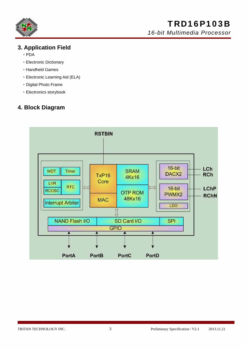
4. Block Diagram

TRD16P103B16-bit Multimedia Processor
TRITAN TECHNOLOGY INC. 4 Preliminary Specification / V2.1 2013.11.21
4.1. Pin Assignments /Description
Pin Name I/O State after
RESET
FUNCTIONS
Chip Power VCC I High Chip Power Input VSS I Low Ground VIO1 I High Chip IO Block Power Input VSS1 I Low Chip IO Block Ground VPPX I U OTP programming Power Supply 7.5V VPD I High PWM Block Power Input VPS I Low PWM Block Ground VCCA I High Analog Block Power Input VSSA I Low Analog Block Ground VIO2 I High Chip IO Block Power Input VSS2 I Low Chip IO Block Ground V33O O High 3.0V Power Supply VDD O High 2.85V Power Supply
Chip Control TESTIN I Low High force chip enter test mode, internal 50K ohm pull-down HALT O Low High presents chip in Halt mode RSTBIN I High Low force chip to enter reset mode, internal 50K ohm pull-up
Clock OSCA I Clock Connect to RC OSC Adjust
General Purpose I/O Port PortA[15:0] I/O Low PortA is programmable Input/Output port PortB[7:0] I/O Low PortB is programmable Input/Output port PortC[7:0] I/O Low PortC is programmable Input/Output port PortD[11:0] I/O Low PortD is programmable Input/Output port
PWM Audio LChP O Low Digital PWM output(+) RChN O Low Digital PWM output(-)
DAC Audio LCh O Low L-Channdel DAC output RCh O Low R-Channdel DAC output
Note: VIO1 and VIO2 must connect to same power source.

TRD16P103B16-bit Multimedia Processor
TRITAN TECHNOLOGY INC. 5 Preliminary Specification / V2.1 2013.11.21
5. Function Descriptions 5.1 TxP16
As shown in the block diagram in Figure 4.1, the TxP16 with MAC module is a 16-bit data width processing
capability and all instructions are operated in one cycle except parameter data ROM(PM) access. The TxP16 not
only provides general arithmetic such as addition, subtraction, shifter, and other logical operations, but it also
involves MAC and circular buffer operations for complexity digital signal processing.
5.2 TxP16 Registers The TxP16 contains of register files are illustrated below:
Figure 5.1 TxP16 Processor Core Registers

TRD16P103B16-bit Multimedia Processor
TRITAN TECHNOLOGY INC. 6 Preliminary Specification / V2.1 2013.11.21
▓ REGISTER FILES DEFINE: AR: Accumulator Register MR2: MUL/MAC Result Register 2 I0: Index 0 Register AX: General AX Register I1: Index 1 Register BX: General BX Register BP: Base Pointer Register CX: General CX Register P0: Pointer 0 Register DX: General DX Register P1: Pointer 1 Register R0: General R0 Register MACOP: MAC Operation Register R1: General R1 Register MACNT: MAC Operation Loop Counter R2: General R2 Register MX: MUL/MAC Input X Register R3: General R3 Register MR0: MUL/MAC Result Register 0 CBL: Circular Buffer Length Register MR1: MUL/MAC Result Register 1 PASR: Parser Register
5.2.1 Special Registers
Accumulator Register The AR is a general-purpose 16-bit register that stores the result of last arithmetic or logical operation. In
addition, any data write to AR will affect the status flag.
Stack Pointer
Figure 5.2 TxP16 Special Registers
The SP is a 4-bit register that is for addressing Stack position. The SP will automatically increment /
decrement cause by instruction “CALL” / “RETS”, and more detail revealed as the “PC Stack” section.
Program Counter
The 16-bit PC register provides 64K-word addressing capability. It is responsible for MCU fetch now
executing instruction.
Program Counter High
The instruction “LJMP” and “LCALL” will reference PCH register to composed of 16-bit pointer provides the
64K words PM addressing range.
Circular Buffer Length Register
Many algorithms such as convolution, correlation, and digital filter require the circular data buffers. The TxP16
supports circular buffer operating via the I0 vs. CIL and P0 vs. CPL. The modulus logic implements automatic
modulus addressing for accessing RM/PM circular buffer data.
TRD16P103B16-bit Multimedia Processor
TRITAN TECHNOLOGY INC. 7 Preliminary Specification / V2.1 2013.11.21
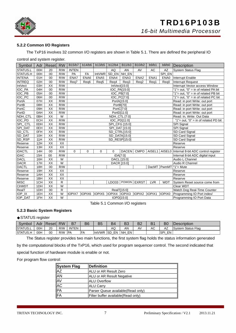
5.2.2 Common I/O Registers
The TxP16 involves 32 common I/O registers are shown in Table 5.1. There are defined the peripheral IO
control and system register. Symbol Adr Reset RW B15/b7 b14/b6 b13/b5 b12/b4 B11/b3 B10/b2 b9/b1 b8/b0 Description
STATUS.L 00H 20 R/W INTEN AQ AN AV AC AZ System Status Flag STATUS.H 00H 00 R/W PA FA IntVWR SD_EN NH_EN SPI_EN INTENA 01H 00 R/W ENA7 ENA6 ENA5 ENA4 ENA3 ENA2 ENA1 ENA0 Interrupt Enable INTREQ 02H 00 R/W Req7 Req6 Req5 Req4 Req3 Req2 Req1 Req0 Interrupt Request IntVect 03H XX R/W IntVect[15:0] Interrupt Vector access Window IOC_PA 04H 00 R/W IOC_PA[15:0] “1”= out, “0” = in of related PA bit IOC_PB 05H 00 R/W IOC_PB[7:0] “1”= out, “0” = in of related PB bit IOC_PC 06H 00 R/W IOC_PC[7:0] “1”= out, “0” = in of related PC bit PortA 07H XX R/W PortA[15:0] Read: in port Write: out port PortB 08H XX R/W PortB[70] Read: in port Write: out port PortC 09H XX R/W PortC[7:0] Read: in port Write: out port PortD 0AH XX R/W PortD[11:0] Read: in port Write: out port NDH_CTL 0BH XX W NDH_CTL [7:0] Read: In, Write: Out Data IOC_PD 0CH XX R/W IOC_PD[11:0] “1”= out, “0” = in of related PD bitSPI_ CTL 0DH XX R/W SPI_CFG [15:0] SPI Signal SPI_DAT 0EH XX R/W SPI_DAT [15:0] SPI Signal SD_CTL 0FH XX R/W SD_CTRL[15:0] SD Card Signal SD_DAT 10H XX R/W SD_DATA[15:0] SD Card Signal SD_RSP 11H XX R/W SD_RESP[15:0] SD Card Signal Reserve 12H XX XX Reserve Reserve 13H XX XX Reserve iDACTL 14H 00 R/W 0 0 0 0 DACEN CMPO AISEL1 AISEL0 Internal 8-bit ADC control register iDAC 15H 00 R/W iDA[7:0] Internal 8-bit ADC digital input DACL 16H XX W DACL [15:0] Audio L Channel DACR 17H XX W DACR [15:0] Audio R Channel DACTL 18H 00 R/W DacMT PwmMT “1”= Mute Reserve 19H XX XX Reserve Reserve 1AH XX XX Reserve Reserve 1BH XX XX Reserve MISC 1CH XX R LDO33 POWON EXRST LVR WDT System Reset source come from ClrWDT 1DH XX W Clear WDT RealT 1DH 00 R RealT[15:0] Watch Dog Real-Time Counter IOP_IX 1EH XX W IOPIX7 IOPIX6 IOPIX5 IOPIX4 IOPIX3 IOPIX2 IOPIX1 IOPIX0 Programming IO Port index/ IOP_DAT 1FH XX W IOPD[15:0] Programming IO Port Data
Table 5.1 Common I/O registers
5.2.3 Basic System Registers
◆STATUS register Symbol Adr Reset RW B7 B6 B5 B4 B3 B2 B1 B0 Description
STATUS.L 00H 20 R/W INTEN AQ AN AV AC AZ System Status Flag STATUS.H 00H 00 R/W PA FA IntVWR SD_EN NH_EN SPI_EN
The Status register provides two main functions, the first system flag holds the status information generated
by the computational blocks of the TxP16, which used for program sequencer control. The second indicated that
special function of hardware module is enable or not.
For program flow control:
System Flag Definition AZ ALU or AR Result Zero AN ALU or AR Result Negative AV ALU Overflow AC ALU Carry PA Parser Queue available(Read only) FA Filter buffer available(Read only)

TRD16P103B16-bit Multimedia Processor
TRITAN TECHNOLOGY INC. 8 Preliminary Specification / V2.1 2013.11.21
System hardware control:
System Flag Definition INTEN System global interrupt control bitIntVWR Interrupt Vector Table access window control bitNH_EN Nand Flash interface enable control bit SPI_EN Serial peripheral interface enable control bit
◆ Address 01H~02H: Interrupt control registers, the detail are illustrated in Interrupt section.
◆ Address 04H~15H: GPIO registers, the detail are illustrated in GPIO section.
◆ Address 16H~18H: DAC control registers, the detail are illustrated in AUDIO section.
◆ System Miscellanea register Symbol Adr Reset RW b15/b7 b14/b6 b13/b5 b12/b4 b11/b3 B10/b2 b9/b1 b8/b0 Description
MISC 1CH XX R LDO33 POWON EXRST LVR WDT System miscellanea register
The system MISC[3:0] register indicates which one is the reset source before DSP system re-boot.
MISC register Definition LDO33 LDO 3.3V supply always ON.(ignore this bit) POWON System Reset from power onEXRST System Reset from external reset pinLVR System Reset from low voltage resetWDT System Reset from watch dog timer
◆ Virtual Programming IO Symbol Adr Reset RW b15/b7 b14/b6 b13/b5 b12/b4 b11/b3 B10/b2 b9/b1 b8/b0 Description
VIO_IX 1EH XX W IOPIX7 IOPIX6 IOPIX5 IOPIX4 IOPIX3 IOPIX2 IOPIX1 IOPIX0 Programming IO Port index VIO_DATA 1FH XX W IOPD[15:0] Programming IO Port Data
Table 5.2 Virtual Programming IO The operation steps of these group register, first select virtual IO port index then write data to programming IO port. Virtual Programming IO Port Symbol Adr Reset RW b15/b7 b14/b6 b13/b5 B12/b4 b11/b3 B10/b2 b9/b1 b8/b0 Description
Timer1 00H XX W Timer0[15:0] Timer1 Timer2 01H XX W Timer1[15:0] Timer2 RTCTimer 02H 00 W - - - - - - DIVSEL1 DIVSEL0 RTC RC-oscillator divider
5.3 PC Stack The PC STACK is TxP16 special embedded memory used to save (PC+1) value, which is composed with
16-level.
Figure 5.3 PC Stack Structure

TRD16P103B16-bit Multimedia Processor
TRITAN TECHNOLOGY INC. 9 Preliminary Specification / V2.1 2013.11.21
Stack's top value is indexed by stack pointer (SP) register. When CALL instruction is executed, then the
(PC+1) will PUSH onto stack addressing by SP and it will auto decrement. At the end of subroutine when RETS
instruction is executed the SP will auto increment and stack content of pointer by SP will POP into PC.
The contents of STACK and SP are neither readable nor writeable by instruction. The SP is initialized to “0”
after RESET. 5.4 Interrupt 5.4.1 Interrupt Vector Table
The Interrupt Vector Table is TxP16 special embedded memory, which is composed with 8-level of FIFO, used
to store the index of interrupt service routine (ISR) address. User can access Interrupt Vector Table by read/write
IntVect I/O register.
Figure 5.4 Interrupt Vector Structure
5.4.2 Interrupt Controller
Common I/O registers Symbol Adr Reset RW B7 B6 B5 B4 B3 B2 B1 B0 Description
STATUS 00H 00 R/W INTEN AN AV AC AZ System Status Flag INTENA 01H 00 R/W ENA7 ENA6 ENA5 ENA4 ENA3 ENA2 ENA1 ENA0 Int Enable INTREQ 02H 00 R/W Req7 Req6 Req5 Req4 Req3 Req2 Req1 Req0 Int Request
This chip provides 8 interrupt sources, user’s program can control 8 interrupts, including 6 internal PWM
Timer, Timer1, Timer2, RTC Timer, SPI and PC Stack Overflow interrupts, and 2 external ExtINT0, ExtINT1,
interrupts. More details control will describe as follows:
Interrupt Source Interrupt Vector Priority PWM Timer 0H INT0_IRQ Timer1 1H INT1_IRQ Timer2 2H INT2_IRQ RTC Timer 3H INT3_IRQ ExtINT0 Port A.b6 4H INT4_IRQ ExtINT1 Port A.b7 5H INT5_IRQ SPI 6H INT6_IRQ PC Stack Overflow 7H INT7_IRQ
Table 5.2 TRD16P103B Interrupt Sources

TRD16P103B16-bit Multimedia Processor
TRITAN TECHNOLOGY INC. 10 Preliminary Specification / V2.1 2013.11.21
(a) Global interrupt enable(INTEN)
The global interrupt INTEN controls the enable/disable of all interrupts. When INTEN is cleared to “0”, all
interrupts are disabled. When INTEN is set to “1”, all interrupts are enabled (but still dependent on value of INTENA
register). The INTEN is initialized to ‘”0” after power on
(b) Interrupt enable (INTENA)
The interrupt enable ENA0, ENA1, ENA2, ENA3, ENA4, ENA5, ENA6, ENA7 are shown in above. An
interrupt is allowed when these control bit are set to “1”, and interrupt is inhibit when these control bit are cleared to
“0”. They are all initialized to “0” after power on.
(c) Interrupt request (INTREQ)
If an interrupt raising edge request is generated, the related interrupt request bit is set to “1” by hardware and
waits for interrupt accept. INTREQ can be cleared to “0” by software. Hardware will not clear this bit. INTREQ are
all initialized to “0” after power on.
5.4.3 Interrupt Processing
When any interrupt request(INTREQ) is generated, the acceptance of interrupt is decided by the interrupt
enable(ENA) and global interrupt enable(INTEN). If the interrupt enable and global interrupt enable related bit are
set to “1”, that interrupt will be accepted on the next clock. These following procedures will automatically be done in
one clock cycle by hardware showing below:
(1) Program Counter(PC), PCH, AR and FLAG will be stored in special hardware registers.
(2) PC will be set to the corresponding interrupt entry address by refer to interrupt vector table.
(3) The global interrupt enable (INTEN) is cleared to “0”, which avoids the nest interrupt happened.
When interrupt service routine was finished, an RETI instruction will perform the procedures by hardware
showing as follows:
(1) Restore the stored PC, PCH, AR and FLAG.
(2) The global interrupt enable (INTEN) is set to “1”, which allows to accept the subsequent interrupt.
Before executing RETI instruction, the corresponding interrupt request (INTREQ) bit must be cleared to “0” by
software. If the request bit is not cleared, the same interrupt will be accepted again.
TRD16P103B16-bit Multimedia Processor
TRITAN TECHNOLOGY INC. 11 Preliminary Specification / V2.1 2013.11.21
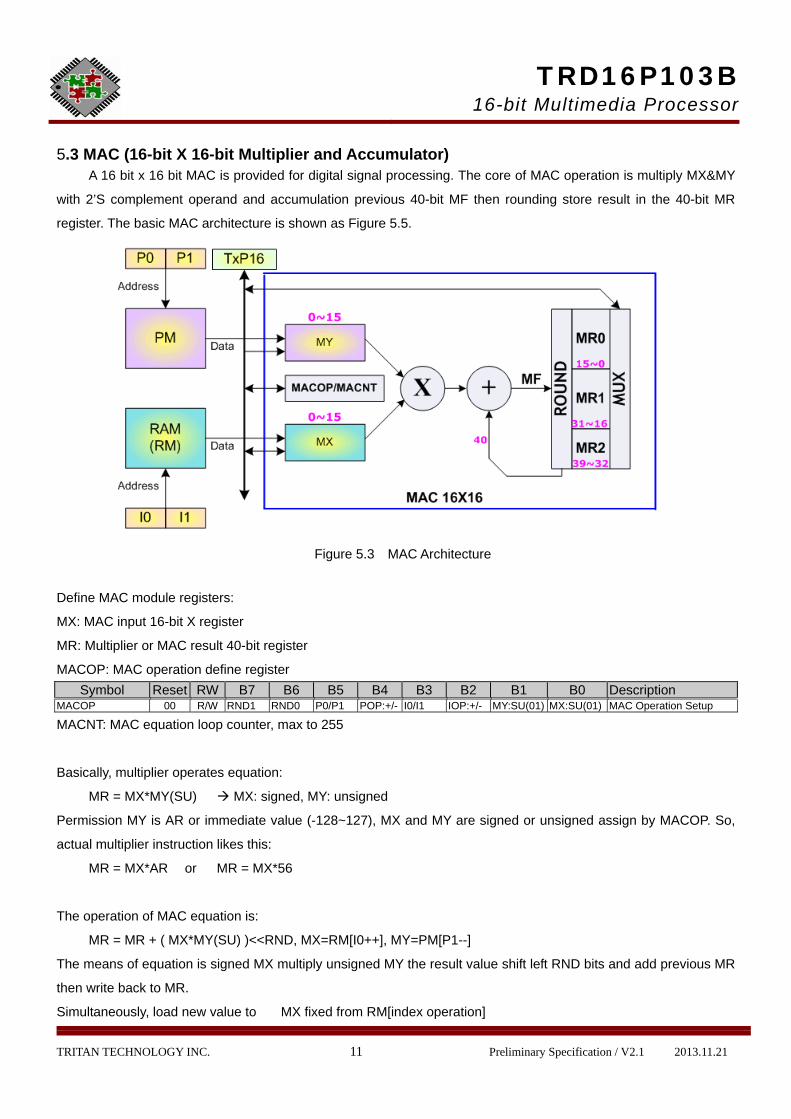
5.3 MAC (16-bit X 16-bit Multiplier and Accumulator) A 16 bit x 16 bit MAC is provided for digital signal processing. The core of MAC operation is multiply MX&MY
with 2’S complement operand and accumulation previous 40-bit MF then rounding store result in the 40-bit MR
register. The basic MAC architecture is shown as Figure 5.5.
Figure 5.3 MAC Architecture
Define MAC module registers:
MX: MAC input 16-bit X register
MR: Multiplier or MAC result 40-bit register
MACOP: MAC operation define register Symbol Reset RW B7 B6 B5 B4 B3 B2 B1 B0 Description
MACOP 00 R/W RND1 RND0 P0/P1 POP:+/- I0/I1 IOP:+/- MY:SU(01) MX:SU(01) MAC Operation Setup
MACNT: MAC equation loop counter, max to 255
Basically, multiplier operates equation:
MR = MX*MY(SU) MX: signed, MY: unsigned
Permission MY is AR or immediate value (-128~127), MX and MY are signed or unsigned assign by MACOP. So,
actual multiplier instruction likes this:
MR = MX*AR or MR = MX*56
The operation of MAC equation is:
MR = MR + ( MX*MY(SU) )<<RND, MX=RM[I0++], MY=PM[P1--]
The means of equation is signed MX multiply unsigned MY the result value shift left RND bits and add previous MR
then write back to MR.
Simultaneously, load new value to MX fixed from RM[index operation]

TRD16P103B16-bit Multimedia Processor
TRITAN TECHNOLOGY INC. 12 Preliminary Specification / V2.1 2013.11.21
MY fixed from PM[pointer operation]
Therefore, MAC array operation like this:
MR = MR + ( MX*MY(SS) ) << 1, MX=RM[I0++], MY=PM[P1--]
MR = MR + ( MX*MY(SS) ) << 1, MX=RM[I0++], MY=PM[P1--]
.
. Successive 64 times
.
MR = MR + ( MX*MY(SS) ) << 1, MX=RM[I0++], MY=PM[P1--]
Actual just one line of instruction present in assembly coding like this:
MACNT = 63
This is very benefit for reducing code size. Of curse, we need setup MACOP register previous; at this example is
like this; Symbol Reset RW B7 B6 B5 B4 B3 B2 B1 B0 Description
MACOP 00 R/W RND1 RND0 P0/P1 POP:+/- I0/I1 IOP:+/- MY:SU(01) MX:SU(01) MAC Operation Setup 0 1 1 1 0 0 0 0
Note: Successive MAC operation will cause MCU interrupt disable.

TRD16P103B16-bit Multimedia Processor
TRITAN TECHNOLOGY INC. 13 Preliminary Specification / V2.1 2013.11.21
6. Memory Configuration 6.1 Internal Program/Parameter Memory
TxP16 consider both instruction and data ROM are the same as program ROM(PM), so it's very flexible and
efficient for instruction and data memory allocation in PM. On the logical PM space is organized into 64kx16-bit
which is addressed by memory address generator unit (MAG). Actual PM is separated into two parts including read
only 48K OTP ROM(Page0) and write available 16-word SRAM(Page1). User can dynamic download program/data
to page1 for MCU get more flexible operation. More details control will describe as follows:
Figure 6.1 TRD16P103B PM block diagram
When TxP16 executed an instruction, the PM address is generated from PC register. Similarity, when it
access a word data, the PM address is composed with 16-bit from P0 or P1. System will auto adjust execute target
space when program context switch between page0 and page1.
6.2.1 Internal Data Working SRAM
The internal data working ram space is totally 4kX16-bit that named as RM. Addressing ranged from 0000H
through 0FFFH, which is generated by Data Address Generator Unit (DAG). Note: Index register (I0,I1,BP) are
16-bit width, but RM address line is only 12-bit width(0~4095); therefore, RM address will be warping when index
value exceed 4095.
Figure 6.2 TRD16P103B RM block diagram

TRD16P103B16-bit Multimedia Processor
TRITAN TECHNOLOGY INC. 14 Preliminary Specification / V2.1 2013.11.21
6.2.2 Data Stack
A Last In First Out (LIFO) STACK is implementation for temporary data storage in RM memory. Generally,
Data Stack is start-up at the bottom of RM, so BP is usually set to 0x0FFF.
Figure 6.3 Data Stack Structure
Data Stack's top value is indexed by base pointer (BP) register. When PUSH instruction is executed, the
“regs” will PUSH onto stack which address by BP and it will auto decrement. If POP instruction is performed, the
BP will auto increment and stack content of pointed by BP will POP into “regs”.

TRD16P103B16-bit Multimedia Processor
TRITAN TECHNOLOGY INC. 15 Preliminary Specification / V2.1 2013.11.21
7. Peripherals
7.1 Programmable Timers Common I/O registers Symbol Adr Reset RW B7 B6 B5 B4 B3 B2 B1 B0 Description
STATUS 00H 0X R/W INTEN AQ AN AV AC AZ System Status Flag INTENA 01H 00 R/W ENA7 ENA6 ENA5 ENA4 ENA3 ENA2 ENA1 ENA0 Int Enable
Virtual Programming IO Port Symbol Adr Reset RW b15/b7 b14/b6 b13/b5 B12/b4 b11/b3 B10/b2 b9/b1 b8/b0 Description
Timer1 00H XX W Timer0[15:0] Timer1 Timer2 01H XX W Timer1[15:0] Timer2 RTCTimer 02H 00 W - - - - - - DIVSEL1 DIVSEL0 RTC RC-oscillator divider
7.1.1 PWM Timer
PWM timer is fixed generate 32kHz interrupt request when INTENA0 bit is turned on, If Auto FIFO_EN is
setting the interrupt request rate = Ft/FIFO_Length.
Figure 7.1 PWM Timer Structure
7.1.2 Timer1 & Timer2
The clock source of Timer1&Timer2 comes from fixed 32.768Mhz, It contains 16-bit write-only counter register.
If Timer enable correspond with the INTENA bit is turned on then counting to time out, an interrupt request will be
generated. At the same time, TnC in Eq.(7.1.1) will be reloaded into Timer register and up-count again. If the global
interrupt enable, an interrupt signal is generated at the next clock.
Int1_Req= 32.768Mhz/(TnC+1) ---- (7.1.1)
Figure 7.2 Timer1&Timer2 Structure

TRD16P103B16-bit Multimedia Processor
TRITAN TECHNOLOGY INC. 16 Preliminary Specification / V2.1 2013.11.21
7.1.3 Low power RC oscillator for RTC Timer
Low power RC oscillator 128KHz is used for generating 1ms, 2ms, 4ms and 64ms interval to wake-up MCU
when in halt mode or interrupt in normal mode. There is about 100% frequency deviation of RC oscillator 128KHz
by different lot or chip. The wake-up function can be disabled by option, default wake-up function is enabled and
INT3_Req is set to high after 2ms when reset occurred. The counter of divider will be reset once while going into
halt mode, and MCU will be wake-up or interrupt after 1ms if DIVSEL1,DIVSEL0=00. Low power RC oscillator is
enabled when MCU in halt mode. The power consumption is about VCC=3V@3uA typically.
DIVSEL1 DIVSEL0 Period 0 0 1ms 0 1 2ms 1 0 4ms 1 1 64ms
Figure 7.3 RTC Timer Structure
Notice: IDE Tool has embedded a demo code to illustrate RTC Timer auto-calibration function.
7.2 General Purpose I/O Ports The TRD16P103B provides 4 I/O ports for user application. There are four I/O port, PA0~PA15, PB0~PB7,
PC0~PC7, and PD0~PD11. The input/output bits programmable by IOC control register respectively. PA0~PA7,
PB0~PB7 wake-up function enable or disable by programmed option, and PA7~ PA6 is external interrupt pin. The
pull-high or pull-low 50k resistor of each pin can be programmed by option. The basic I/O schematic is showed in
Figure 7.4.
These totally 44 I/O pins work not only just a general input/output port function but also can configure to SD
controller, NAND Flash , Serial Flash/ROM interface. For more detail please refer to relative section.
Figure 7.4 Basic I/O Configuration
PB0,PB1 support two edge modes for wake-up function are rising and falling edge trigger. The rising
and falling edge trigger is selected by option.

TRD16P103B16-bit Multimedia Processor
TRITAN TECHNOLOGY INC. 17 Preliminary Specification / V2.1 2013.11.21
The PortA0~PortA7 also provides 4 comparators configuration for user application that each comparator enable or
disable by programmed option.
Figure 7.5 Comparator Configuration
7.3 Extension Device TRD16P103B built-in special hardwires for external device connection capability are listed below: 7.3.1 NAND Flash Interface
In order to enable NAND Flash interface, user should set STATUS.b11 = 1 before NAND Flash operation. Symbol Adr Reset RW B7 B6 B5 B4 B3 B2 B1 B0 Description
NDH_CTL 0BH XX R/W NDH_CLE
NDH_ALE
NDH_REN
NDH_WEN
NDH_RST
NAND Flash RE/WE control signal
Programmer could set NDH_CTL control register which the correspond control signal will mapping to
PortC[7:0] , PortD[7:4]. I/O Port NAND Flash Direction Description
PortC[7:0] D[7:0] IO Data bus D0~D7 PortD.7 CLE O Command Latch Enable Signal PortD.6 ALE O Address Latch Enable Signal PortD.5 WE O Write Signal PortD.4 RE O Read Signal PortA.3 RDY I Flash ready(free assign by user)
The actual NAND Flash control timing see as below:

TRD16P103B16-bit Multimedia Processor
TRITAN TECHNOLOGY INC. 18 Preliminary Specification / V2.1 2013.11.21
/RE=1
/WE
D[7:0] Data
Data Write Timing
CLE,ALE=0
/RE
/WE=1
D[7:0] Data
Data Read Timing
CLE,ALE=0
/RE=1
/WE
D[7:0] CMD
CLE Write Timing
CLE
/RE=1
/WE
D[7:0] ADRESS
ALE Write Timing
ALE
Figure 7.5 NAND Access Timing
For instance: Assume we perform the operations of NAND Flash’s CMD write are coding like these
SET io[NDH_CTL].b4 force CLE=1,WE=0 and PortC will set out-port direction automatically
io[PortC] = CMD Command output
SET io[NDH_CTL].b0 reset interface, force CLE=0, ALE=0, WE=1, RE=1
For instance: Assume we perform the operations of NAND Flash’s DAT write are coding like these
SET io[NDH_CTL].b1 force WE=0 and PortC will set out-port direction automatically
io[PortC] =DAT Data output
SET io[NDH_CTL].b0 reset interface, force CLE=0, ALE=0, WE=1, RE=1
For instance: Assume we perform the operations of NAND Flash’s DAT read are coding like these
SET io[NDH_CTL].b2 force RE=0 and PortC will set in-port direction automatically
Reg=io[PortC] Data input, the force WE=1, RE=1
7.3.2 SPI Controller
In order to enable SPI Controller interface, user should set STATUS.b8 = 1 before SPI Controller operation.
7.3.2.1 Features
• Designed for read-only and read/write data
• Support MXIC Serial Flash
• Serial clock rate: 32.768 MHz / 16.384 MHz / 13.107 MHz / 10.922 MHz / 8.192 MHz / 4.096 MHz • Built in 4x16 bits data buffer

TRD16P103B16-bit Multimedia Processor
TRITAN TECHNOLOGY INC. 19 Preliminary Specification / V2.1 2013.11.21
Type1: I/O Port SPI interface Direction Description
PortA.0 SO I Serial Data output to MCU PortA.1 SI O Serial Data input from MCU PortA.2 SCK O Serial Clock PortA.3 CS O Chip Select(free assign by user)
Type2: I/O Port SPI interface Direction Description
PortB.0 SO I Serial Data output to MCU PortD.0 SI O Serial Data input from MCU PortD.1 SCK O Serial Clock PortD.4 CS O Chip Select(free assign by user)
Notice: The SIP Configurations Type1 or Type2 is assign by option.
7.3.2.2 Control/Data Registers Symbol Adr Reset RW b15/b7 B14/b6 b13/b5 b12/b4 b11/b3 B10/b2 b9/b1 b8/b0 Description
CTRL_W.L 0DH 01 W - CLR RCV SEND Total Send/Receive Byte Control Register Low Byte CTRL_W.H 0DH 00 W Mode CKSEL ICS - - - Control Register High Byte CTRL_R.L 0DH 00 R DATOK CLR RCV SEND Total Send/Receive Byte Read Status Low Byte CTRL_R.H 0DH 00 R Mode CKSEL ICS - BFINX1 BFINX0 Read Status High Byte
Total Send/Receive Byte: Total byte number of sending or receiving.
ICS: Internal SPI command select enable.
SEND: Trigger sending data.
RCV: Trigger receiving data.
CLR: Clear control flag.
CKSEL: (000: 32.768MHz), (001: 16.384MHz), (010: 13.107 MHz), (011: 10.922 MHz), (100: 8.192 MHz), (101:
4.096 MHz).
Mode: (0:Posedge latch data), (1:Negedge latch data).
DATOK: Indicate transmit/receive data O.K.
BFINX [1:0]: Indicate which data buffer is accessed by CPU. Symbol Adr Reset RW b15/b7 b14/b6 b13/b5 b12/b4 b11/b3 B10/b2 b9/b1 b8/b0 Description
DATA_R 0EH XX W DATA[15:0] Write Transmission Data Value DATA_R 0EH XX R DATA[15:0] Read Received Data Value
DATA [15:0]: Transmit/Receive Data Value
Notice that more detail SPI operation sequence, please ref. Appendix.

TRD16P103B16-bit Multimedia Processor
TRITAN TECHNOLOGY INC. 20 Preliminary Specification / V2.1 2013.11.21
7.3.3 SD Card Controller
In order to enable SD Controller interface, user should set STATUS.b12 = 1 before SD Controller operation. I/O Port SD Name Direction Description
PortA.[13:10] D[3:0] IO Data bus D0~D7 PortA.14 CMD IO Command PortA.15 CLK O CLK Signal
7.3.3.1 Features
• Memory capacity: Standard Capacity SD Memory Card: Up to and including 2 GB
• Designed for read-only and read/write cards
• Support 1 serial data line or 4 parallel data lines
• SD clock rate 0 -16 MHz, up to 8 MB/sec (max) interface speed (using 4 parallel data lines) • Card Detection (Insertion/Removal)
• Built in 8x16 bits data buffer
7.3.3.2 Control/Data Registers
Symbol Adr Reset RW b15/b7 b14/b6 b13/b5 b12/b4 b11/b3 B10/b2 b9/b1 b8/b0 Description SD_CTL 0FH 00 W COMMAND[15:0] Write Command Value SD_CTL.L 0FH X0 R DATIN3 DATIN2 DATIN1 DATIN0 0 BFINX2 BFINX1 BFINX0 Read Status Low Byte SD_CTL.H 0FH 00 R 0 0 0 0 0 COMOK DATOK RESOK Read Status High Byte
COMMAND [15:0]: Transmission Command Value
DATIN [3:0]: SD Card serial data input.
BFINX [2:0]: Indicate which data buffer is accessed by CPU.
COMOK: Indicate command transmission O.K.
DATOK: Indicate transmit/receive data O.K.
RESOK: Indicate receive response O.K. Symbol Adr Reset RW b15/b7 b14/b6 b13/b5 b12/b4 b11/b3 B10/b2 b9/b1 b8/b0 Description
SD_DAT 10H XX W DATA[15:0] Write Transmission Data Value SD_DAT 10H XX R DATA[15:0] Read Received Data Value
DATA [15:0]: Transmit/Receive Data Value Symbol Adr Reset RW b15/b7 b14/b6 b13/b5 b12/b4 b11/b3 B10/b2 b9/b1 b8/b0 Description
SD_RSP.L 11H 00 W - - - - - - CKOFF CKSEL Set SD Clock SD_RSP 11H 00 R RESPONSE[15:0] Read Response Value
CKSEL: (0: identification frequency 0-400kHz), (1: data transfer frequency).
CKOFF: (0: SD Clock generation), (1: SD Clock shut down).
RESPONSE [15:0]: Received Response Value

TRD16P103B16-bit Multimedia Processor
TRITAN TECHNOLOGY INC. 21 Preliminary Specification / V2.1 2013.11.21
7.4 Audio Output The four configurations of audio output form in TRD16P103B system are stereo 16-bit PWM, stereo 15-bit
PWM, mono 16-bit PWM and stereo 16-bit DAC. The kind of solution is determined by user’s application. Notice
that each time there is only one type of PWM can be specified, which assign by option. The PWM PIN configuration
shows as below:
Figure 7.6 PWM output configuration
7.4.1 Stereo PWM Output
Two 16-bit resolution of PWM converters are built-in TRD16P103B for stereo audio application. In order to get
more output power driving, which require external amplifier for stereo output pin.
Additionally, two 15-bit of PWM amplifiers(Type4) are also built-in TRD16P103B for stereo audio application.
Common I/O registers Symbol Adr Reset RW b15/b7 b14/b6 B13/b5 b12/b4 B11/b3 b10/b2 b9/b1 b8/b0 Description
DACL 16H XX W DACL [15:0] DAC Audio L Channel DACR 17H XX W DACR [15:0] DAC Audio R Channel
7.4.2 Mono PWM Output A 16-bit of PWM amplifiers is built-in(Type3) TRD16P103B system. This amplifier can be used to direct drive 8
ohm speaker without any external circuit.

TRD16P103B16-bit Multimedia Processor
TRITAN TECHNOLOGY INC. 22 Preliminary Specification / V2.1 2013.11.21
Common I/O registers Symbol Adr Reset RW b15/b7 b14/b6 b13/b5 b12/b4 B11/b3 b10/b2 b9/b1 b8/b0 Description
DACL 16H XX W DACL [15:0] 16-bit PWM Channel
7.4.3 Stereo DAC Output Two 16-bit of digital-to-analog convert are built-in TRD16P103B for stereo audio application. In order to get
more output power driving, which require external amplifier for stereo output pin LCh and RCh.
Common I/O registers Symbol Adr Reset RW b15/b7 b14/b6 B13/b5 b12/b4 B11/b3 b10/b2 b9/b1 b8/b0 Description
DACL 16H XX W DACL [15:0] DAC Audio L Channel DACR 17H XX W DACR [15:0] DAC Audio R Channel

TRD16P103B16-bit Multimedia Processor
TRITAN TECHNOLOGY INC. 23 Preliminary Specification / V2.1 2013.11.21
7.5 Auto-FIFO The Auto-FIFO allows user transfer base on 4-level of data to PWM D/A. In some case of frame base
applications that data transfer is more efficient than sample base. It is advantageous to decrease number of context
switch between main program and interrupt service routine (ISR). The FIFO structure reveal as below:
Figure 7.7 Auto FIFO Structure
An interrupt is generated when an entire 4-level FIFO is transfer completed (D\A FIFO buffer is empty), then
interrupt service routine should re-load 4-level data to FIFO at ones during 32K sample period. The FIFO will
automatically shift-out data to PWM D/A at each sample period.
Note: Auto-FIFO is enable/disable by option setup up.
Note: Emulator doesn’t support PWM Mute function for emulation, user need to notice this difference
between Emulator and Real Chip.

TRD16P103B16-bit Multimedia Processor
TRITAN TECHNOLOGY INC. 24 Preliminary Specification / V2.1 2013.11.21
7.6 Simple three channel 8 bits ADC Symbol Adr Reset RW B7 B6 B5 B4 B3 B2 B1 B0 Description
iDACTL 14H 00 R/W 0 0 0 0 DACEN CMPO AISEL1 AISEL0 Internal 8-bit ADC control register iDAC 15H 00 R/W iDA[7:0] Internal 8-bit ADC digital input
The simple 8 bits ADC function can be consist of 8 bits DAC, MUX, comparator, sample and an ADC
converting program. The comparator positive pin is connected to 8 bits DAC, and the negative pin is connected to
MUX. The 8 bits DAC can generate 256 steps from 0 to VCC analog signal control by register i8DA[7:0], Three
channel analog input is by way of MUX to negative input of comparator. ADC converting data output is get from
adjusting ADC register iDA[7:0] continuous to approach the analog input level ( the negative pin of comparator ) by
reading comparator out register CMPO. These blocks is enabled by DACEN=1, and power down by halt mode or
DACEN=0. This function will be power down in halt mode automatically.
Figure 7.8 Simple three channel 8 bits ADC block diagram
The original foundry calibration ADC maximum converting voltage is based on 5V± 100mV.
8 bit ADC DC electrical characteristics Parameter Condition Min. Typ. Max Unit
VREF CP trim 5 ± 0.1 V 1 LSB (5 ± 0.1)/256 19.5 mV
AISEL1 AISEL0 channel input 0 0 VCC 0 1 PA6 1 0 PA7

TRD16P103B16-bit Multimedia Processor
TRITAN TECHNOLOGY INC. 25 Preliminary Specification / V2.1 2013.11.21
8. System Control 8.1 Halt Mode & Wake up The TRD16P103B is changed into HALT mode (system clock stop, RTC stop by Option setup) when HALT
instruction executed. It provides a power saving mode for those applications requiring a very low stand-by current.
The RTC timer, PA0~PA7 and PB0~PB7 are supporting the wake-up MCU function when related I/O port
raising/falling edge which selects by option. The program counter will be 04H when HALT instruction executed
immediately; in addition, MCU will release HALT state and program counter go-to next address after 16us stable
clock(system clock) when wake up condition occurred. During the Halt mode period, the SRAM will keep their
previous data without changing, yet INTENA register will auto clearly.
8.2 Watch Dog Timer Reset (WDT) Symbol Adr Reset RW b15/b7 b14/b6 b13/b5 b12/b4 B11/b3 b10/b2 b9/b1 b8/b0 Description
ClrWDT 1DH XX W Clear WDT RealT 1DH 0000 R RealT[15:0] Watch Dog Real-Time Counter
The watch dog timer (WDT) is used to reset whole chip when detect unexpected execution sequence of
instructions caused by accident condition, avoiding dead lock of MCU program. Software shall run an "clear watch
dog timer"( CLRWDT ) instruction before this timer time out. It will generate a reset signal to reset whole system
when WDT overflow.
WDT will be reset when wake-up from halt or after power on or software clear. In test mode, watch dog timer
will be disabled no matter watch-dog-timer is time-out or not. If programmer read the “RealT” register, it can get the
content of watch dog timer base on 31.25us.
The reset watch dog timer code syntax is strongly recommended as: “CLRWDT = AR”.
8.3 Low Voltage Reset When VCC power is applied to the chip, the low voltage reset is initially enabled by default, it will be disabled
when in halt mode. The internal system reset will be generated if VDD power below about 2.2v .
The normal operation of LVR is always enable expect disable in HALT mode.
8.4 Reset System
The TRD16P103B reset is come from four signals which are power on reset, low voltage reset(LVR), external
“RSTBIN” pin and WDT overflow reset. A dedicated resetb input pin is provided to reset this chip. For normal
operation of this chip, a good reset is needed. This pin has 50K ohm pull up resistor. The operation frequency of
MCU will go back to OTP page mode when reset occurred.

TRD16P103B16-bit Multimedia Processor
TRITAN TECHNOLOGY INC. 26 Preliminary Specification / V2.1 2013.11.21
Figure 8.1 Reset system block diagram
8.5 Clock System Architecture The TRD16P103B clcok system provides 32.768 MHZ System-Clock and 128KHz Real-Time-Clock. The RC
oscillator frequency can be optional adjustment by external OSCA pin.
Figure 8.2 Clock System Configuration

TRD16P103B16-bit Multimedia Processor
TRITAN TECHNOLOGY INC. 27 Preliminary Specification / V2.1 2013.11.21
9. Electrical Characteristics 9.1 Absolute Maximum Rating
Parameters Symbol Value Unit DC Supply Voltage VCC <6 V Input Voltage Vin -0.5 to VDD+0.5 V Operating Temperature Range Ta 0 to 75 ℃ Storage Temperature Range Tstg -50 to 150 ℃
9.2 DC/AC Characteristics VCC=3.0V, Ta=25℃ unless otherwise noted
Parameters Symbol Minimum Typical Maximum Test Condition Operating range VCC 2.4 V - 6 V RC oscillator frequency
Frc1 10.92MHz±3%
Low power RC oscillator frequency
Frc2 128KHz ±100%
Halt Current Ihalt1 <3uA 5uA All function off VPPX pin programming voltage
VPPX 7.5 ±0.25V
Operating Current Iop 11mA no load input high voltage Vih 0.8 VCC input low voltage Vil 0.2 VCC input leakage Current
Ilk 0.1 uA
output high voltage Voh 0.95 VCC no load output low voltage Vol 0.05 V no load output high current1 Ioh 12 mA Vout=2.4V,
PortA[15:0],PortD[11:0]output high current2 Ioh 5.4 mA Vout=2.4V,
PortB[7:0],PortC[7:0] output low current1 Iol -20 mA Vout=0.8V
PortA[15:0],PortD[11:0]output low current2 Iol -8 mA Vout=0.8V
PortB[7:0],PortC[7:0] pull-down resistance Rpd 110K ohm 150 K ohm
@3V 250 K ohm@6V, 2.4V
pins with pull-down, Port A,B,C,D
Notice that PA.2 and PD.1 have more two times of driving capability.

TRD16P103B16-bit Multimedia Processor
TRITAN TECHNOLOGY INC. 28 Preliminary Specification / V2.1 2013.11.21
10. Development Support TRITAN TRD16P103B TM family series are supported with full range of hardware and software development tools:
Integrated Development Environment (IDE)
- TRD16DevIDE software
TRD16DevIDE contains
- TxPASM Assembler
- TxPCC C Compiler
- TxPLink Object Linker
- TxPLib Library Management
Simulator
- TRD16SIM software Simulator
Emulator
- TRD16ICE circuit hardware Emulator
- Emulator doesn’t support PWM Mute function for emulation, user need to notice this
difference between Emulator and Real Chip.

TRD16P103B16-bit Multimedia Processor
TRITAN TECHNOLOGY INC. 29 Preliminary Specification / V2.1 2013.11.21
Application Circuit: Application Circuit 1.a : Stereo 16-bit PWM AMP output with Serial Flash (Type1)
Application Circuit 1.b : Stereo 16-bit DAC AMP output with Serial Flash(Type2)

TRD16P103B16-bit Multimedia Processor
TRITAN TECHNOLOGY INC. 30 Preliminary Specification / V2.1 2013.11.21
Application Circuit 1.c : Stereo 15-bit PWM output with Serial Flash
Application Circuit 1.d : Mono16-bit PWM output with Serial Flash

TRD16P103B16-bit Multimedia Processor
TRITAN TECHNOLOGY INC. 31 Preliminary Specification / V2.1 2013.11.21
Application Circuit 2.a : Mono 16-bit PWM output with Nand Flash
Application Circuit 2.b : Stereo 16-bit PWM AMP output with Nand Flash
TRD16P103B16-bit Multimedia Processor
TRITAN TECHNOLOGY INC. 32 Preliminary Specification / V2.1 2013.11.21
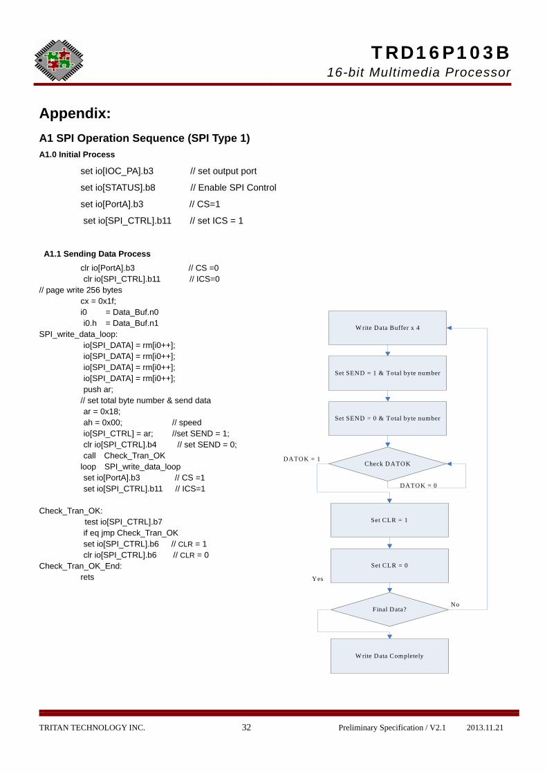
Appendix: A1 SPI Operation Sequence (SPI Type 1) A1.0 Initial Process set io[IOC_PA].b3 // set output port
set io[STATUS].b8 // Enable SPI Control
set io[PortA].b3 // CS=1
set io[SPI_CTRL].b11 // set ICS = 1
A1.1 Sending Data Process clr io[PortA].b3 // CS =0 clr io[SPI_CTRL].b11 // ICS=0 // page write 256 bytes cx = 0x1f; i0 = Data_Buf.n0 i0.h = Data_Buf.n1 SPI_write_data_loop: io[SPI_DATA] = rm[i0++]; io[SPI_DATA] = rm[i0++]; io[SPI_DATA] = rm[i0++]; io[SPI_DATA] = rm[i0++]; push ar; // set total byte number & send data ar = 0x18; ah = 0x00; // speed io[SPI_CTRL] = ar; //set SEND = 1; clr io[SPI_CTRL].b4 // set SEND = 0; call Check_Tran_OK loop SPI_write_data_loop set io[PortA].b3 // CS =1 set io[SPI_CTRL].b11 // ICS=1 Check_Tran_OK: test io[SPI_CTRL].b7 if eq jmp Check_Tran_OK set io[SPI_CTRL].b6 // CLR = 1 clr io[SPI_CTRL].b6 // CLR = 0 Check_Tran_OK_End: rets
W rite Data Buffer x 4
Check DATOK
DATOK = 0
DATOK = 1
Final Data?
Yes
W rite Data Completely
No
Set SEND = 1 & Total byte number
Set SEND = 0 & Total byte number
Set CLR = 1
Set CLR = 0
TRD16P103B16-bit Multimedia Processor
TRITAN TECHNOLOGY INC. 33 Preliminary Specification / V2.1 2013.11.21
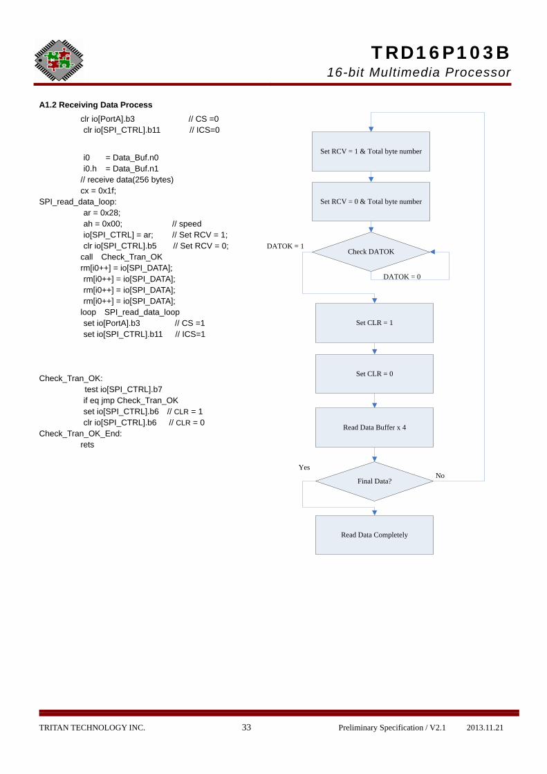
A1.2 Receiving Data Process clr io[PortA].b3 // CS =0 clr io[SPI_CTRL].b11 // ICS=0
i0 = Data_Buf.n0 i0.h = Data_Buf.n1 // receive data(256 bytes) cx = 0x1f; SPI_read_data_loop: ar = 0x28; ah = 0x00; // speed io[SPI_CTRL] = ar; // Set RCV = 1; clr io[SPI_CTRL].b5 // Set RCV = 0; call Check_Tran_OK rm[i0++] = io[SPI_DATA]; rm[i0++] = io[SPI_DATA]; rm[i0++] = io[SPI_DATA]; rm[i0++] = io[SPI_DATA]; loop SPI_read_data_loop set io[PortA].b3 // CS =1 set io[SPI_CTRL].b11 // ICS=1 Check_Tran_OK: test io[SPI_CTRL].b7 if eq jmp Check_Tran_OK set io[SPI_CTRL].b6 // CLR = 1 clr io[SPI_CTRL].b6 // CLR = 0 Check_Tran_OK_End: rets
Check DATOK
DATOK = 0
DATOK = 1
Final Data?
Yes
Read Data Completely
No
Read Data Buffer x 4
Set RCV = 0 & Total byte number
Set RCV = 1 & Total byte number
Set CLR = 1
Set CLR = 0

TRD16P103B16-bit Multimedia Processor
TRITAN TECHNOLOGY INC. 34 Preliminary Specification / V2.1 2013.11.21
12. Revision history
REVISION DESCRIPTION PAGE DATE
V1.1 New establish 2010/8/18
V1.2 Change V27O to 2.7V 4 2010/11/18
V1.3 Exchange NAND Flash Read/Write Description 17 2011/04/08
V1.3 Change Pin name VDD to V27O All 2011/04/08
V1.3 ADC source selection change to 0~2 24 2011/04/08
V1.4 Compatible PWM driver 2 2011/12/09
V1.5 Change Pin name V27O to VDD All 2012/01/30
V1.6 Modify VDD, V33O output voltage to 2.9V and 3.5V
LDO 3.3V supply always enable
2,4,8 2012/04/26
V1.7 Modify max. operation frequency to 11Mhz 2 2012/06/04
Emulator doesn’t support PWM Mute function for emulation 23, 28 2012/06/25
V1.8 Modify V33O=3.2V 2,8 2012/10/05
Modify RTC accuracy from 30% to 100% 2,16,27 2012/10/05
Adding ADC electrical characteristics description 24 2012/10/05
V1.9 Change Reset Capacitor value to 103 All 2013/03/21
V2.0 Change IOC_PD to R/W type 7 2013/05/31
V2.1 Modify V33O=3.0V 2,4 2013/11/21