tramp-8 8 band cw transceiver - qrpproject.de · 3 revision: june 16. 2007 the tramp-8 cw...
TRANSCRIPT

1
Revi
sion
: ju
ne 1
6. 2
007
DL-QRP-AG
© QRPproject Motzener Straße 36-38 12277 Berlin http://www.QRPproject.de Telefon: +49(30) 85 96 13 23 e-mail: [email protected] by: FIservice Peter Zenker DL2FI email:[email protected]
Tramp-88 Band CW Transceiver
Revi
sion
: Ju
ne 1
6. 2
007
2
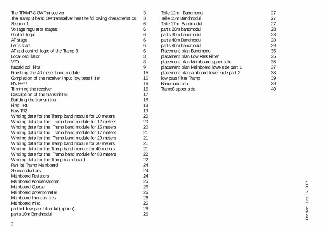
The TRAMP-8 CW Transceiver 3The Tramp 8 band CW transceiver has the following characteristics: 3Section 1 6Voltage regulator stages: 6Control logic 6AF stage 6Let´s start: 6AF and control logic of the Tramp 8 6Local oscillator 8VFO 8Neosid coil kits 9Finishing the 40 meter band module 15Completion of the receiver input low pass filter 16PAUSE!!! 16Trimming the receiver 16Description of the transmitter: 17Building the transmitter. 18First TR1 18Now TR2 19Winding data for the Tramp band module for 10 meters 20Winding data for the Tramp band module for 12 meters 20Winding data for the Tramp band module for 15 meters 20Winding data for the Tramp band module for 17 meters 21Winding data for the Tramp band module for 20 meters 21Winding data for the Tramp band module for 30 meters 21Winding data for the Tramp band module for 40 meters 21Winding data for the Tramp band module for 80 meters 22Winding data for the Tramp main board 22Partlist Tramp Mainboard 24Semiconductors 24Mainboard Resistors 24Mainboard Kondensatoren 25Mainboard Quarze 26Mainboard potentometer 26Mainboard Inductivities 26Mainboard misc. 26partlist low pass filter kit(option) 26parts 10m Bandmodul 26
Teile 12m Bandmodul 27Teile 15m Bandmodul 27Teile 17m Bandmodul 27parts 20m bandmodul 28parts 30m bandmodul 28parts 40m Bandmodul 28parts 80m bandmodul 29Placement plan Bandmodul 35placement plan Low Pass Filter 35placement plan Mainboard upper side 36placement plan Mainboard lowe side part 1 37placement plan ainboard lower side part 2 38low pass filter Tramp 39Bandmodulfoto 39Tramp8 upper side 40

3
Revi
sion
: ju
ne 1
6. 2
007
The TRAMP-8 CW Transceiver- tentative english translation by Peter Raabye, OZ5DW, 18.04.03Not verbatim: readability was a priority.
Designed by Peter Solf, DK1HE, devoted to DL-QRP-AG und QRPprojectProject coordination and editing: Peter Zenker, DL2FIWith support from Jürgen, DL1JGS (Prototypes, manual)Manual by FIservice
Preface by DK1HEWhen you look at contemporary QRP rigs, you will find three broad catego-ries:1. Monobanders (about 60%)2. Multiband rigs, switchable by interchangeable modules (about 25 %)3. „Real“, knob switchable multiband rigs (about 15%)
Every ham who have tried working with the first two categories in multi-band setups, know the problem of fast band changes: The “we’ll be in touchshortly” in another band is difficult, especially, when working portable.Often you haven’t packe the “proper” transciever or the band module justisn’t there in the back pack. These problems, which I have encounteredmyself, and the fact that DL-QRP-AG presented me with a request for aswitchable multiband CW transciever, prompted me to develop one.The basic project was a tribander with the given name Tramp 3. At Ham-Radio 2001, I had the opportunity to discuss my project with the wellknown QRP-AG developers Ulli/DK4SX and Helmut/DL2AVH. This resulted ina redesign of the T/R switch and the IF regulator. Thanks a lot for the goodadvice! Peter/DL2FI found an enclosure with optimal size for QRP work.Because of the small size of this enclosure, SMD parts were inavoidable.During the further design process, it became clear, that the systematic useof SMD technology left enough room for an 8 band design in the chosenenclosure. Tramp 8 was born!
The Tramp 8 band CW transceiver has the followingcharacteristics:
- 8 SW bands (160m_10m) selectable from the front panel- Thanks to modular design, expandable in sections (1_8 Band modules)- Nice measures: 150 x 165 x 50 mm W x D x H- Optional DDS VFO
- Optional digital frequency display- Low power consumption by reciever (important, when running from
rechargeable batteries)- 3 section band filter in RX gives high mirror selectivity- Double superheterodyne, first IF 4915 KHz, second IF 455 KHz- 500 Hz crystal filter in first IF stage- Dynamic range overall about 100 dB- Manual adjustment of IF amplification- AGC drawn from second IF- Field strength display- Two stage AF filtering with a band width of 250 Hz, center frequency
adjustable- AF output 0,5 W- VFO range about 100 kHz- RIT- Transmitter output continously variable up to a max. of 8 Watts- Transmitter soft keying - QSK!- Output power indicator- CW side tone- Supply voltage 11_15VWe have tried to cover all areas in this manual. Please take the time to readthe manual. The Tramp 8 isn’t difficult to build, there are a few catches,though, and it will certainly be helpful to think each section over beforeyou start building.A large pledge to you: Please help us to make the handbook better. Write uswith any suggestion for improvement, report every mistake!PLEASE read the “builders tips” shipped with the kit, before warming upyour soldering iron. This section contains important information, that couldbe the key to succesful completion of your kit. Take your time to workthrough this material.Should you come up with any problems or suggestions for improvement,please turn to Peter, DL2FI , he’ll be glad to help you.You can reach QRPeter either (and best!) via e-mail [email protected] or by phone at +49(30)85961323
Revi
sion
: Ju
ne 1
6. 2
007
4
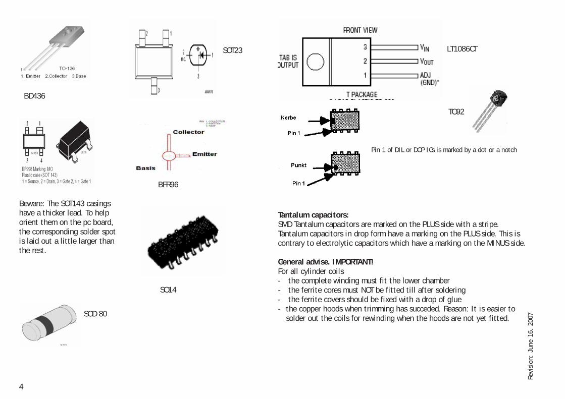
Beware: The SOT143 casingshave a thicker lead. To helporient them on the pc board,the corresponding solder spotis laid out a little larger thanthe rest.
Tantalum capacitors:SMD Tantalum capacitors are marked on the PLUS side with a stripe.Tantalum capacitors in drop form have a marking on the PLUS side. This iscontrary to electrolytic capacitors which have a marking on the MINUS side.
General advise. IMPORTANT!For all cylinder coils- the complete winding must fit the lower chamber- the ferrite cores must NOT be fitted till after soldering- the ferrite covers should be fixed with a drop of glue- the copper hoods when trimming has succeded. Reason: It is easier to
solder out the coils for rewinding when the hoods are not yet fitted.SOD 80
SOT23
BD436
BFR96
SO14
LT1086CT
TO92
Pin 1 of DIL or DOP ICs is marked by a dot or a notch

5
Revi
sion
: ju
ne 1
6. 2
007
ceramic trimer cap. Drawing shows minimum

Revi
sion
: Ju
ne 1
6. 2
007
6
Section 1
We begin with the voltage regulators, the AF sectiona and the control logicof the Tramp 8: Let get familiar with the function of the individual stages.
Voltage regulator stages:To make the voltage dependent parameters of the transmitter and recieverindependent of the supply voltage, all critical parts are supplied from a lowdrop IC voltage regulator with an output of 10 Volts. This means that thecompleted kit will run on 11 to 15 Volts. This reduces the usability ofcommon rechargeable batteries, as the should not be discharged below 10,8Volts, and on the other hand won’t deliver more than some 14 Volts. The +8Volts supply from IC13 goes to the tuning voltage of the VFO. The filteringcircuit R113-C134 reduces the noise on the regulator voltage. The wishedfrequency range of the VFO is tuned by P9 (band spread). The voltageregulater IC12 serves as a +6 Volts supply for IC1 and IC10.
Control logicWhen grounding the key input at pin 21, pin 3 of IC3 goes high and swit-ches T11 on through R36. C42 will charge quickly through R35 with theconsequence that pin 4 of IC3 also goes high. The differential amplifier T9-T10 will be switched through R33-R32, that is T9 takes over the totalcurrent (T10 blocks), and turns on T7. This opens for the stabilized +10Volts for the Transciever as the +10V ‘S’ supply. When the grounding isterminated, pin3 of IC3 goes low and blocks T11. C42 discharges with atime constant adjustable by P3 (T/R delay). When reaching the triggeringvoltage of the following nand gate, the output at pin 4 will go low andblock the differential amplifier T9-T7. T10 takes over the total current andthus switches T8 on, so that the stabilized +10 Volts will become +10 Volts‘E’ for the transceiver.
AF stageThe output voltage of the CW filter is passed via the volume control to theAF amplifier IC4. The stage will output 500 mW into an 8 ohm load. T13serves for muting the AF during transmission. This will reduce keying clicksin the AF output.
Let´s start:
AF and control logic of the Tramp 8
Begin by mounting the parts for the voltage controllers. Even though youread through the previous, check and double check, the parts before solde-ring in. A check with the parts list will help to avoid wrong placement ofcomponents. Especially important are the ceramic capacitors, which have noprinted marking. You can find the place and orientation for each componentfrom the print on the pc board and the placement diagram.Put in all components, presented ind the diagram for the AF and controllogis. There are not anything special around here.
[ ] solder in pc board pins at all places in the pc board marked by num-bers.Place low profile parts first. If you are a beginner for SMT parts, please readour little SMT manual. You will find it in the little introduction brochureshipped with any QRPproject kit. I am pretty sure, everyone will find somenice, helpfull tricks in there.
[ ] T 8 BD436 [ ] T 9 BC846B SOT23[ ] T 10 BC846B SOT23 [ ] T 11 BC846B SOT23[ ] T 12 BC846B SOT23 [ ] T 13 BC846B SOT23[ ] T 14 BC846B SOT23 [ ] T 15 BC846B SOT23[ ] D 9 1N5402 [ ] D 11 LL4148[ ] R 25 120R 0805 [ ] R 26 820R 1206[ ] R 27 12k 0805 [ ] R 28 12k 0805[ ] R 29 820R 0805 [ ] R 30 10k 0805[ ] R 31 10k 0805 [ ] R 32 10k 0805[ ] R 33 6k8 0805 [ ] R 34 5k6 0805[ ] R 35 39R 0805 [ ] R 36 18k 0805[ ] R 37 33k 0805 [ ] R 38 56R 0805[ ] R 39 22k 0805 [ ] R 40 100k 0805[ ] R 41 22k 0805 [ ] R 42 12k 0805[ ] R 43 3R3 1206 [ ] R 44 82k 0805[ ] R 45 [ ] R 47 4R7 1206[ ] R 48 22k 0805 [ ] R 49 12k 0805[ ] R 50 27k 0805 [ ] R 51 56R 0805[ ] R 52 4k7 0805 [ ] R 53 4k7 0805
7
Revi
sion
: ju
ne 1
6. 2
007
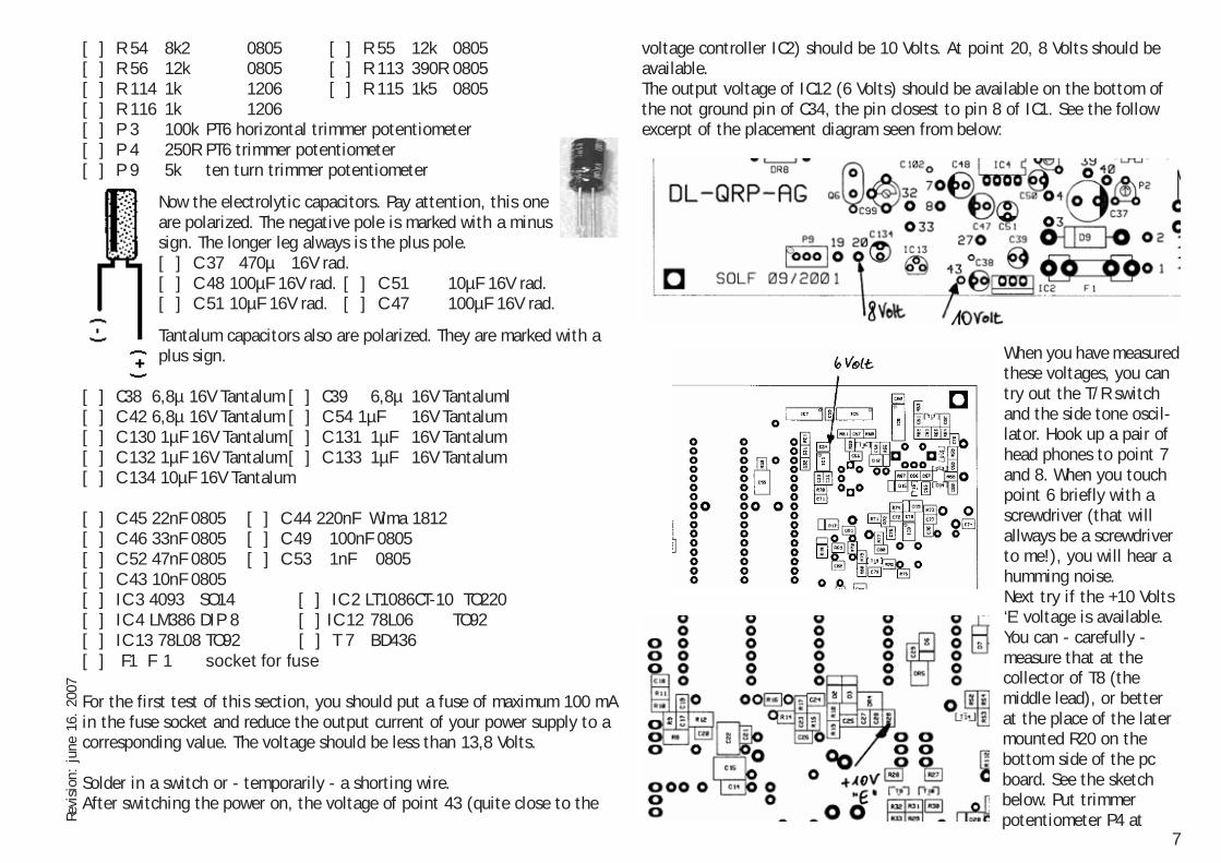
[ ] R 54 8k2 0805 [ ] R 55 12k 0805[ ] R 56 12k 0805 [ ] R 113 390R 0805[ ] R 114 1k 1206 [ ] R 115 1k5 0805[ ] R 116 1k 1206[ ] P 3 100k PT6 horizontal trimmer potentiometer[ ] P 4 250R PT6 trimmer potentiometer[ ] P 9 5k ten turn trimmer potentiometer
Now the electrolytic capacitors. Pay attention, this oneare polarized. The negative pole is marked with a minussign. The longer leg always is the plus pole.[ ] C 37 470µ 16V rad.[ ] C 48 100µF 16V rad. [ ] C 51 10µF 16V rad.[ ] C 51 10µF 16V rad. [ ] C 47 100µF 16V rad.
Tantalum capacitors also are polarized. They are marked with aplus sign.
[ ] C38 6,8µ 16V Tantalum [ ] C39 6,8µ 16V Tantaluml[ ] C 42 6,8µ 16V Tantalum [ ] C 54 1µF 16V Tantalum[ ] C 130 1µF 16V Tantalum[ ] C 131 1µF 16V Tantalum[ ] C 132 1µF 16V Tantalum[ ] C 133 1µF 16V Tantalum[ ] C 134 10µF 16V Tantalum
[ ] C 45 22nF 0805 [ ] C 44 220nF Wima 1812[ ] C 46 33nF 0805 [ ] C 49 100nF 0805[ ] C 52 47nF 0805 [ ] C 53 1nF 0805[ ] C 43 10nF 0805[ ] IC 3 4093 SO14 [ ] IC 2 LT1086CT-10 TO220[ ] IC 4 LM386 DIP 8 [ ] IC 12 78L06 TO92[ ] IC 13 78L08 TO92 [ ] T 7 BD436[ ] F1 F 1 socket for fuse
For the first test of this section, you should put a fuse of maximum 100 mAin the fuse socket and reduce the output current of your power supply to acorresponding value. The voltage should be less than 13,8 Volts.
Solder in a switch or - temporarily - a shorting wire.After switching the power on, the voltage of point 43 (quite close to the
voltage controller IC2) should be 10 Volts. At point 20, 8 Volts should beavailable.The output voltage of IC12 (6 Volts) should be available on the bottom ofthe not ground pin of C34, the pin closest to pin 8 of IC1. See the followexcerpt of the placement diagram seen from below:
When you have measuredthese voltages, you cantry out the T/R switchand the side tone oscil-lator. Hook up a pair ofhead phones to point 7and 8. When you touchpoint 6 briefly with ascrewdriver (that willallways be a screwdriverto me!), you will hear ahumming noise.Next try if the +10 Volts‘E’ voltage is available.You can - carefully -measure that at thecollector of T8 (themiddle lead), or betterat the place of the latermounted R20 on thebottom side of the pcboard. See the sketchbelow. Put trimmerpotentiometer P4 at

Revi
sion
: Ju
ne 1
6. 2
007
8
approximately thecenter position andhook up a morse keyfrom point 21 toground. When youoperate the key, youwill hear the sidetone in the headphones. The volumecan be adjusted byP4, and isn’t depen-dent on the volume
control of the AF stage.Now check the +10 Volts ‘S’ voltage, while actuating the morse key. Thisvoltage is switched by T7, where you - again carefully - can measure it atthe collector (middle transistor lead). Another measuring point is at DR7 intthe following sketch:
Local oscillatorThe necessary local oscillator signals for transmission and reception iscreated with the use of a PLL stabilized oscillator stage directly on theproper frequency. This gives a reduction of harmonics with no need forfurther filtering.The stage is almost identical to the one used in the Black Forest transciever.The VCOs of the band modules are based on the T2 MOSFET, to offset thefirst IF (4915 kHz) to the proper output frequency. The oscillator proper is aHartley design. D5 stabilizes the amplitude. The signal at R7 goes via theswitching diode D6 to the VCO mixer via the cascode coupling of T2, Thisgives a good isolation of the VCO output from the oscillator resonant cir-cuit.The tuning diode D4 is coupled so strongly to the VCO circuit at L4-C18,that it gives the VCO range a tuning possibility. Through this measure, ansafe phasing is achieved at the VCO stabilizer. The band set oscillator alsofound on the band module, swings by T1 and Q1 to a frequency some 3915kHz lower as the shown lower band edge of the VCO. C14 - DR1 blocksovertone crystals from oscillating at their 1. harmonic (at least necessary inthe 10 and 12 meter bands). The crystal oscillator signal at R6 is coupled tothe band set - XO mixer via the switching diode D3. At IC1 VCO and bandset - XO frequencies are mixed.
The mixer output resonant circuit L4-C35 selects the difference frequencyand gives a VFO range of 2915-4015 kHz. The amplifying stage T16, whichis inductively coupled to L4, serves to amplify the mixer output signal to alevel proper for the following 128:1 divider IC6. At the output IC6 a signalclose to 31 kHz is available to lead on to the frequency/phase comparatorIC7. The second input of IC7 gets another 31 kHz signal from dividing theVFO frequency (3915-4015 kHz) by 128 in IC8. Depending on the directionof the difference between real (output at IC6) and wanted frequency (out-put at IC8) gives a proportional regulating voltage, which after filtering inthe loop filter R57-R58-C55 trims the VCO, so that the two 31 kHz signalsare in phase. If the VFO frequency changes, the VCO frequency will changeas much. As both VCO and band set XO is changed for every band, the sameVFO tuning range will do for all bands.
VFOThe VFO is a Hartley based on JFET T18. D15 is used to stabilize the ampli-tude. The degree of feed back is chosen, so that the lowes possible powerlevel is achieved, and as little RF heating of the frequency determiningparts as possible. The tuning diodes D13-D14 works back to back to reducethe RF amplitude changes to a minimum. The band spread is set up withC67 so, that it in conjunction with L5 it will give a tuning range of about3915-4015 kHz. The RIT tuning diode is coupled loosely over D16, whichcan shift the reception frequency +/- 1,5 kHz with respect to the transmit-ting frequency. The following JFET buffer T17 amplifies the via C63 looselycoupled VFO signal to the level necessary to trigger IC8. At the same time itreduces influence backwards in the oscillator stage. Through R66-D112-C64the VFO gets a highly stable and noise free supply voltage.
Now mount one of the band module pc boards with the coil and othercomponents necessary for frequency determination. We recommend, thatyou begin with the 40 meter module.
[ ] T 1 BFS20 SOT23 [ ] T 2 BF989 SOT143[ ] D 3 BA679S SOD80 [ ] D 4 BBY40 SOT23[ ] D 5 LL4148 SOD80 [ ] D 6 BA679S SOD80
Attention: You will solder a first Xtal now. If you use too much solder itmay happen, that solder gets between the Xtal case and the PCB. This willcause a short. To prevent, use the little silicon isolation pads if you canfind them in the kit. Due to some problems to get them, some kits will not

9
Revi
sion
: ju
ne 1
6. 2
007
contain this isolation pads. If so, solder the can with a little distance tothe PCB. A good trick is to use a piece of wire (a leg of a resistor will befine) to keep the distance. Dont forget to remove the distance wire aftersoldering the Xtals can. This trick is good for all Xtal cans.
[ ] Q 1 Band set crystal 8,000 MHz ( for the 40m band)
[ ] R 3 68k 0805 [ ] R 4 27k 0805[ ] R 5 1k 0805 [ ] R 6 10R 0805[ ] R 7 47R 0805 [ ] R 8 68R 0805[ ] R 9 2k2 0805 (see appendix) [ ] R 10 56k 0805[ ] R 11 100k 0805 [ ] R 12 150k 0805[ ] C 9 film trimcap 30pF red [ ] C 10 33pF 0805[ ] C 11 220pF 0805 [ ] C 12 150pF 0805[ ] C 13 entfällt [ ] C 14 22nF 0805[ ] C 15 22nF 0805 [ ] C 16 22nF 0805[ ] C 17 220pF 0805 (see appendix) [ ] C 18 68pF 0805[ ] C 19 15p 0805 [ ] C 20 4n7 0805[ ] C 21 10nF 0805 [ ] Dr 1 left out[ ] Dr 2 replaced by 1n5 1206 [ ] Dr 3 47µH 1210[ ] Dr 4 47µH 1210 [ ] Dr5 47µH 1210[ ] connector, 16 pins
The next will be to wind VCO coil L4. But before proceeding to that, pleaseread the following theory:
Neosid coil kits
Every coil kit contains basically the coil form with 5 leads, a screen can, aferrit core and a ferrite cover, also known as a covering core (???). For somecoils the covering core is removed, but a core is always used. Further anunderlay disc is used. This is used to avoid shorts from the screen can tothe pc board. Many users use these discs, others throw them away andinsted solders the screen with a little distance to the pc board.
The example is for the standard S7 forms, which will be used in the IFstages. For the band modules we will use Neosid coils instead, as they are alittle lower.The coils are generally wound in the lower chamber, the turns are usuallywound in one layer, which means turn lies below turn. On top of means on
top of, and not in in an outer layer. Be careful, that the cold end of thecoils are connected to the right pin. Which is the cold end of a coil? Thecold end is the end of the coil closest to ground. As we are dealing withradio frequencies, the ground connection can be direct or through a capaci-tor of say some 100 nF. That is equal from an RF stand point, as such acapacitor has nearly no resistance for RF.If the lower chamber cant hold all of the turns, the rest of the turns shouldbe wound backwards down from the top end of the first layer, as a secondlayer.I recommend to look up the correct connections, and not just accept theseinformations. You only learns from what you do, and maybe the next kitwon’t have as good a manual as the Tramp manual.
1=screen can2=covering core3=core4=coil form
A look at the diagram shows us, thatone side of the coil is directly wiredto ground. This is the cold end of theprimary. Now you have to find thecorresponding lead of the coil form.
The picture shows a view of the leads from BELOW. Put the pc board infront of you, so that the free space for L4 is upwards. When you put thecoil form in the holes for L4, and looks at it from the bottom of L4, you seesomething like in the drawing. Now look carefully, which pin goes to whichpart, and compare to the diagram: The pin at the lower left goes to grao-ind, that is the cold end, and the beginning of the coil. The lower middlepin goes to R8 and C16, that is the pin for the tap. The lower right pingoes to C17/C18/C19, here goes the end of the coil.When you have located the pins, you can begin winding the coil. Take the0,2 mm lacquered copper wire out of the bag, and straighten it by gentlypulling it between thumb and index finger. Be careful not to create littlebends. Tin some 2 cm of the wire end. Begin by winding from the bottomtowards the top of the coil form. Put the first 2-3 turns tightly around the

Revi
sion
: Ju
ne 1
6. 2
007
10
starting pin. Pull the wire through the notch in thecoil form after putting on 4 turns. Now comes thetap. Make a 3 cm loop on the wire, and twist it. Thistwisted end it put through the notch to the startingpin, where it is put around the pin three times. Asclose as possible to the bottom plate. Then the next12 turns are put on top in the same direction as thefirst 4. Then after the 16. turn put the end of the
wire through the notch to the proper pin. Tin the wire end, and put threeturns around the starting pin, and cut wire (leave some 3 cms). The coilsshould now be fixed to the coil form. It is recommended to use a time triedmethod: drown the coil in bees wax. This can be bought at hobby shops.Now the wire ends can be soldered to the leads. Tin lightly, solder quickly!When the wire ends are fastened, the coil is placed in the correct holes, andsolder from the pc board bottom side.Solder time about 2 seconds per lead. Do not place the screen cans yet,that should only be done on completion of the functional test.
Put the band module aside, and finish the VFO coils and the output trans-former of the PLL mixer.
The coil form for the VFO coil L5 is easily recognized, at it is the largest inthe kit (type 10). This coil comes with a short trimming core F10b with aviolet colour coding (GW3X6), it is the sam type as for the small coils usedin the band modules.The VFO coils is wound in the same way as the previously wound coil of theband module.
Coil L5 seen from below.
For the VFO coil use the thin 0,1 mm copper wire. Thetotal number of turns are 60, the tap is 15 turns from the
cold end, the cold end is at the bottom! Don’t forget to treat the finishedcoil with bees wax.
Now comes the output tranformer of the PLL premixer, L4.This transformer is as easy to wind as the previously built coils.
Begin by idenfying the proper coil form. It is one of the left ones with alarger height.The primary has 24 turns of the 0,1 mm copper wire, previously used for theVFO coil. This winding must be placed on the coil form first. The secondaryconsists of 12 turns, placed on the middle of the primary.Our building suggestion for this coil looks like this:
Coil form seen from below.
Remember to put the covering core on the coil after fixing the coils withbees wax. Stick the covering cores on with a LITTLE UHU Plus glue (orequivalent).
Now follows the frequency determining components for the main pc board.The following components must be soldered to the main pc board.
[ ] IC 1 NE 612 [ ] IC 6 4060[ ] IC 7 4046 [ ] IC 8 4060[ ] T 16 BFS 20 [ ] T 17 MMBF 4416[ ] T 18 MMBF 4416 [ ] D 12 BZV55 6,8[ ] D 13 BBY 40 [ ] D 14 BBY 40[ ] D 15 LL 4148 [ ] D 16 BBY 31[ ] R 21 1k8 0805[ ] R 57 47k Layer resistor on top of board[ ] R 58 4k7 0805 [ ] R 59 100k 0 805[ ] R 60 1k5 0805 [ ] R 61 1M 0805[ ] R 62 1M 0805 [ ] R 63 1k 0805[ ] R 64 470R 0805 [ ] R 65 100k 0805[ ] R 66 390R 0805 [ ] R 67 100k 0805[ ] R 68 68k 0805 [ ] R 69 68k 0805[ ] C 31 1nF 0805 [ ] C 32 10nF 0805[ ] C 33 1nF 0805 [ ] C 34 47nF 0805[ ] C 35 270pF 0805 [ ] C 55 220nF Wima 1812[ ] C 56 10nF 0805 [ ] C 57 10nF 0805

11
Revi
sion
: ju
ne 1
6. 2
007
[ ] C 58 100nF 0805 [ ] C 59 100nF 0805[ ] C 60 100nF 0805 [ ] C 61 10nF0805[ ] C 62 22nF 0805 [ ] C 63 6p80805[ ] C 64 47µF 16V electrolytic, radial[ ] C 65 22nF 0805[ ] C 66 68pF 0805 [ ] C 67 150pF0805[ ] C 68 22nF 0805 [ ] C 69 12pF0805[ ] C 70 22nF 0805[ ] L 4 PLL premixer output transformer[ ] L 5 VFO-coil[ ] 16 pole edge connector (pull out surplus pins)
Hook up the potentiometer for the RIT (2k2), and, as it is needed for thetest and trimming of the VFO, also the 10 turn trimming potentiometer,which should be hooked up to point 17, 19 and 20.Here we’ll describe a variant of the trimming of the VFO, but more ways arepossible. For others, you will need further preparations.Put the band module on its connector. Hook up the corresponding voltage(point 9...16) sot point 43, to supply voltage to the band module. Put theRIT potentiometer in center position and the 10 turn potentiometer fortuning in its leftmost position.
Now solder a capacitor of 47 nF from the last pin of the band module toground. This is necessary, as we first with the completion and mounting ofall 8 band modules have the massed parallel capacity of the C20’s to sufficefor the loop filter. The capacitor can be left in place with no resultingproblems.
For this tuning variation, you will need an oscilloscope with a sufficingband width (the VCO of the 10 meter module swing at more than 33 MHz),and a frequency counter. When you have prepared this, set the currentlimiter on the power supply to 100 mA, this is more than enough. Alterna-tively put in a quick fuse of this value.Check the pc boad and the band module for solder bridges, and for allcomponents to have all leads soldered.
Switch on the power supply and check the current drawn by the application.This current should be well below 100 mA. If no current is drawn or signifi-
cantly more, quickly turn off powerand locate the error.
No smoke?Congratulations, let’s continue!To switch on the switching diode ofthe band set oscillator, we need totemporarily connect the DC connec-tion. Use a 1,8k resistor from thecathode of D6 to ground. In thefinished setup, this resistor isreplace by R70/R71/R72 on the mainpc board.Check the next function of the bandset oscillator. Connect the probe ofthe oscilloscope to pin 1 of one ofthe free band module connectorspaces. There you should find apulsed voltage of som 30..50 mV p-p.Remove the probe of the oscilloscopeand hook up your frequency counter
in the same place. Trim the band setoscillator to the crystal frequencyneeded. The necessary change is achie-ved in trimming C9 on the band modu-le.Hook up your oscilloscope to pin 7 ofthe band module connector and checkif the VCO of the band module oscilla-tes at all.
Revi
sion
: Ju
ne 1
6. 2
007
12
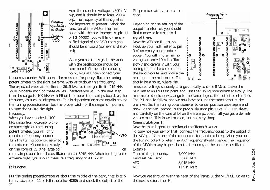
Here the expected voltage is 300 mVp-p, and it should be at least 200 Vp-p. The frequency of this signal isnot important at present. Cehck thefunction of the VFO on the mainboard with the oscilloscope. At pin 11of IC( (4060), you will find the am-plified signal of the VFO, the signalshould be sinusoid (somewhat distor-ted).
When you see this signal, the workwith the oscilloscope should beterminated. At the last measuringpoint, you will now connect your
frequency counter. Write down the measured frequency. Turn the tuningpotentiometer to the right extreme. Also write down this frequency.The expected value at left limit is 3915 kHz, at the right limit 4015 kHz.You’ll probably not find these values. Therefore you will in the next steptrim the range to 100 kHz with P9 on the top of the main pc board, as thefrequency as such is unimportant. This is dependent on some details aroundthe tuning potentiometer, but the proper width of the range is importantto tune the VFO to the rightfrequency.When you have reached a 100kHz range from extreme left toextreme right on the tuningpotentiometer, you will onlytheed the frequency counter.Turn the tuning potentiometer tothe extreme left and tune slowlyon the core of L5 (the large coil onthe main pc board) til the oscillator runs at 3915 kHz. When turning to theextreme right, you should measure a frequency of 4015 kHz..It is done!
Put the tuning potentiometer at about the middle of the band, that is at 5turns. Locate pin 11 of IC6 (the other 4060) and check the output of the
PLL premixer with your oscillos-cope.
Depending on the setting of theoutput transformer, you shouldfind a more or less sinusoidsignal there.Now the VFO can fill its job.Hook up your multimeter to pin3 of an empty band modulesocket. You will find either novoltage or some 10 Volts. Turnslowly and carefully with yourtuning tool in the core of L4 ofthe band module, and notice thereading on the multimeter. Theshould be a point, where themeasured voltage suddenly changes, ideally to some 5 Volts. Leave themultimeter on this test point and turn the tuning potentiometer slowly. Themultimeter should now change to the same degree, the potentiometer does.The PLL should follow, and we now have to tune the transformer of thepremixer. Set the tuning potentiometer to center position once again andhook ud the oscilloscope to the previously used pin 11 of IC6. Turn slowlyand carefully on the core of L4 on the main pc board, till you get a definiti-ve maximum. This is well marked, but not very sharp.Congratulations!!!Now the most important section of the Tramp 8 works.To convince your self of that, connect the frequency count to the output ofthe VCO (pin 7 in one of the connectors for band modules). When you turnthe tuning potentiometer, the VCO frequency should change. The frequencyof the VCO is alway higher than the frequency of the band set oscillator.Example:Transmitting frequency 7,000 MHzBand set oscillator 8,000 MHzVFO 3,915 MHzVCO 11,915 MHz
Now you are through with the heart of the Tramp 8, the VFO/PLL. Go on tothe next section, the IF.

13
Revi
sion
: ju
ne 1
6. 2
007
IF Section
In the IF, we use the ‘bedrock” TCA440 (IC5). Even though it is a vintage 25years, is still has an unbeaten performance. Originally made for AM recepti-on, it contains the following parts:
- AGC regulated input with a 40 dB dynamic range- doubly balanced mixer with fine large signal behaviour- oscillator stage- 3 stage AGC regulated 455 kHz IF amplifier with a 60 dB dynamic range- AGC derived from IF- output for a field strength indicator
QRPProject have reserved a larger stock of these, to be able to meet de-mands for some time.
Via L7-C94 the 4915 kHz IF signal goes to the input of IC5. The integratedoscillator resonates with Q6 on 5368 kHz. The 455 kHz IF signal is filteredby L8-C108 and inductively coupled to the input of the IF amplifier (pin12). The amplified 455 kHz signal is available over L9-C102. Via C103 thesignal is led to the active AGC rectifier at T21. This stage works as a voltagefollower and allows a quick rise in AGC at C107. A manually supplied regula-ting voltage is added to the dynamic AGC voltage at point 32. The inputstage and the second IF amplifier are supplied with the AGC voltage inparallel, giving a dynamic range of more than 100 dB! At pin 10 of IC5, wehave a DC voltage proportional to the amplitude of the recieved signal, forattachment of a field strength meter. Through P6, the field strength metercan be calibrated (up to 300 microamperes). Via a secondary on L9 1/8 ofthe IF voltage is coupled into the following product detector for demodula-tion. The MOSFET T22 works as a multiplikative mixer. The BFO signal entersgate 2 of T22 via C118. The demodulated AF signal is led via R98 to the CWfilter. C121 serves as a bypass for any left over 455 kHz signals. The JFETT23 forms a Colpitts oscillator governed by the ceramic resonator Q7. D20serves to stabilize the amplitude and to clean up the spectral purity of theBFO output signal. P5 and C115 works as an adjustable phasing network,whose variable part makes it possible to pull the 455 kHz resonator some 2kHz. Experiments with capacitative trimmers gave unhandy values.
Begin populating the IF section
[ ] IC 5 TCA 440 (A 244) please install only the socket, not yet the IC -this will be done later[ ] IC 11 TL072 SO8 [ ] T 21 BC 846 B[ ] T 22 BF 989 [ ] T 23 MMBF 4416[ ] T 24 BC 846 B [ ] D 20 LL 4148[ ] D 21 LL 4148 [ ] Q 6 5,3680[ ] Q 7 CSB 455 ceramicResonator[ ] R 85 18k 0805[ ] R 86 8k2 0805 [ ] R 87 1k8 0805[ ] R 88 39R 0805 [ ] R 89 68k 0805[ ] R 90 56k 0805 [ ] R 91 220R 0805[ ] R 92 100k 0805 [ ] R 93 1k 0805[ ] R 94 1k5 0805 [ ] R 95 27k 0805[ ] R 96 220k 0805 [ ] R 98 1k 0805[ ] R 99 120R R0805 [ ] R 10039k 0805[ ] R 101 12k 0805 [ ] R 102 33k 0805[ ] R 103 39k 0805 [ ] R 104 1k2 0805[ ] R 105 82k 0805 [ ] R 106 39k 0805[ ] R 107 1k2 0805 [ ] R 108 82k 0805[ ] R 109 10k 0805 [ ] R 110 10k 0805[ ] R 111 120R 0805 [ ] R 112 15k 0805[ ] P 5 2k Minipot [ ] P 6 2k5 PT6-horizontal pot[ ] P 7 2k Minipot [ ] P 8 2k Minipot[ ] C 94 220pF 0805 [ ] C 95 22nF 0805[ ] C 96 120pF 0805 [ ] C 97 120pF0805[ ] C 98 27pF 0805 [ ] C 99 60pF Filmtrimmer[ ] C 100100nF 0805 [ ] C 1012,2µF 1206 10V Tantal[ ] C 1021800pF Styroflex 63V[ ] R 88a 2k7 1206 (extra, for mounting parallel to C102)[ ] C 10310nF 0805 [ ] C 104 100nF 0805[ ] C 10522nF 0805 [ ] C 106 47nF 0805[ ] C 1074,7µF 1206 6,3V Tantal[ ] C 1081800pF Styroflex 63V[ ] C 10910nF 0805 [ ] C 110 100nF 0805[ ] C 111 100nF 0805 [ ] C 112 4,7µF1206 6,3V Tantal[ ] C 113 47nF 0805[ ] C 114 10µF 16V rad. Electrolytic

Revi
sion
: Ju
ne 1
6. 2
007
14
[ ] C 115 100pF 0805 [ ] C 116 220pF 0805[ ] C 117 47nF 0805 [ ] C 118 100pF 0805[ ] C 119 100nF 0805 [ ] C 121 100nF 0805[ ] C 122 100µF 16V rad. Electrolytic[ ] C 123 15nF film 5%[ ] C 124 15nF film5%[ ] C 125 15nF film 5%[ ] C 126 15nF film 5%[ ] C 127 1µF 1206 16V Tantalum[ ] C 128 100µF 16V rad. electrolxtic[ ] C 129 2,2µF 1206 10V tantalum[ ] C 135 100nF 0805[ ] Dr8 470µH SMCC
L8 and L9 are premade coils for the second IF, - no winding by hand![ ] L 8 Neosid BV 00530700[ ] L 9 Neosid BV 00530700
The input coil for the IF IC, L7, is once more a coil to wind yourself. Usethe already described method.Please identify the right coil form. It is a 7 mm form with a larger height,than the ones used for the band modules. The primary has 20 turns of thesame 0,1 mm copper wire as used for the VFO coil and for the PLL premixer.
This winding must be placed on the form first. Pleasealso remember to place the wire as close to the leads ofthe form as possible, to reduce the distance betweenthe pc board and the coil body.The secondary consists of 5 turns of 0,1 mm copperwire. Our building suggestion looks like this:
Finishing the receiver part of the main pc board.
We suggest, that you once more begin by making the necessary coils. Beginwith the transformer for the receiver mixer, L6. Find the proper coil form:You need a 7 mm form with the large height. Tin the some 2 cm of 0,1 mmlacquered copper wire and wind it about three turns around the post at thelead. Then pull the wire to the upper chamber of the coil form and wind on
20 close turns, beginning from below. Then draw the wire on to the lead,tin it on a proper length and wind it around the lead and solder it to thelead.The transformer L6 secondary is next. Tin another bit of 0,1 mm copperwire, wind 3 turns on the relevant lead and put 6 turns on the center partof the primary. Then draw the wire to the proper lead, twist it around thelead and solder it in place. Finish by fixing the turns with bees wax, andglue on the covering core. Put an isolating disc under the coil form and
solder L6 to the main pc board. PLEASE DO NOTYET SOLDER IN THE SCREEN CAN.Our building suggestion for L6 on the main boardlooks like this, Coil seen from below
Now make TR6, the input transformer for the reciever mixer. This transfor-mer is wound on a black FT37-77 toroid. By now you have wound that manycoils, that a toroid will pose no problem. Here are our directions:
Cut some 25 cm of 0,2 mm copper wire and tin one end. Take the core inone hand and put the soldered end through it. That is the first turn. Holdon to this wire end and the core and take the other end of the wire in theother hand. Now you have to pull the entire length of the wire through thecore. Pull it tight, but take care not to scratch the lacquer on the wire. Thiswas the second turn. You will only need 10 more. Before pulling the nextturn through, remember to space the turns on the core instead of placingthem close to one another. The drawing gives a clue, but doesn’t show theright number of turns.If you plan properly, you won’t have to space the turns afterwards, eventhought it is possible to some degree. The turns shouldn’t risk cutting.WInd the rest of the secondary, cut the free end with enough left for solde-
ring to the pc board. I usually mark the secondaryby folding back the free ends after winding thecoil. Now put on the primary with its 6 turns. Do itin the same way as the secondary, just winding theprimary on the existing turns of the secondary.
Example of a secondary on a toroid

15
Revi
sion
: ju
ne 1
6. 2
007
Tin the ends and solder the transformer to the main board. Put in the restof the parts for the receiver.
[ ] IC 10 NE612 SO8 [ ] T 20 MMBF4416 SOT23[ ] D 1 LL4148 SOD80 [ ] D 2 BA679S SOD80[ ] D 3 BA679S SOD80 [ ] D 4 LL4148 SOD80[ ] D 5 LL4148 SOD80 [ ] D 6 BZV55 C5,1 SOD80[ ] D 7 BZV55 C5,1 SOD80 [ ] D 8 LL4148 SOD80[ ] D 18 BA679S SOD80[ ] Q 1 4915,2kHz Filter crystal[ ] Q 2 4915,2kHz Filter crystal[ ] Q 3 4915,2kHz Filter crystal[ ] Q 4 4915,2kHz Filter crystal[ ] R 20 820R 0805[ ] R 22 after measurement, depends on instrument[ ] R 23 330R 0805[ ] R 24 1k2 1206 [ ] R 70 1k5 0805[ ] R 71 180R 0805 [ ] R 72 39R 0805[ ] R 82 220R 0805 [ ] R 83 100k 0805[ ] R 84 1k 0805 [ ] R 97 820R 0805[ ] P 2 10k PT6-L Piher PT 6 horizontal[ ] C 27 47nF 0805 [ ] C 28 47nF 0805[ ] C 29 47nF 0805 [ ] C 30 47nF 0805[ ] C 36 47nF 0805 [ ] C 71 22nF 0805[ ] C 83 1nF 0805 [ ] C 84 47nF 0805[ ] C 85 220pF 0805 [ ] C 86 15pF 0805[ ] C 87 10nF 0805 [ ] C 88 47nF 0805[ ] C 89 220pF 0805 [ ] C 90 220pF 0805[ ] C 91 220pF 0805 [ ] C 92 220pF 0805[ ] C 93 220pF 0805 [ ] C 120 47nF 0805[ ] RL1 Reed-Rel. 12V 1xUm. [ ] DR4 100µH 1210[ ] DR5 100µH 1210 [ ] DR6 100µH 1210
Now finish the 40 meter band module. If you chose another band, use thevalues for that band instead. The manual supposes that you chose 40 meters.
Finishing the 40 meter band module
The resistor, you temporarily soldered to the band module must be removed.Only a few components remain and the coils to wind. Lets begin with these.
Finish L1 for the chosen band module.Follow the now known method, which wewill summarize here. L1 has the hot enddownwards. Our building suggestion isfound to the right, seen from below.Choose the right coil form. It should be a
low 7 mm form, lower than those used on the main board. Finish the prima-ry. Use 0,1 mm copper wire. Tin the first 2 cms of wire, fix it with threeturns around the lead and solder it to the lead. Begin winding as close tothe bottom of the form as possible. Wind the coil with the proper number ofturns and draw the wire to the bottom of the form, twist it around the leadand solder it in.I do know, that it is a little boring to read the same instructions over andover, but it is exactly as important as boring. There isn’t much room in theTramp, and a few mm means the difference between placing all of the bandmodules or not.The secondary should once more begin by tinning the wire and twisting itaround the lead post. Use 0,1 mm copper wire, and begin above the top ofthe primary. Check the number of turns in the table for the proper bandmodule.Draw the wire down to the lead after winding the proper number of turns,twist the wire 3 times around the lead post and solder it in. The secondaryis NOT a second layer on the primary, but wound above the primary but inthe same chamber of the form.You have remembered to secure the turns with bees wax and glueing thecovering core, right? Solder the coil to the band module. Why so muchhaste? Well: L1 has the same number of turns, but the leads have a diffe-rent orientation. That is why you shouldn’t mix up the two coils!
Finish L3. It has the same number ofturns as the previous coil, follow theabove description, but do check thebuilding suggestion and solder the leadsin the proper orientation. After finishingit, you should solder the coil on to theband module board.

Revi
sion
: Ju
ne 1
6. 2
007
16
Now only L2 is left. This is the simplest coil with only one turn.OK, you know by now: tin 2 cm of wire, twist around the right lead andsolder. draw the wire to the body of the form and put on the proper numberof turns for the band module. Pull the wire downwards, twist it around the
lead and solder it in.Put on the bees wax and glue in the covering core.Now put in the trimming core and the screen can.Solder L2 to the band module board. Our buildingsuggestion looks as this, coil seen from below
This done, you only need to put in a few components and the band moduleis finished.
[ ] D 1 BA679S [ ] D 2 BA679S[ ] R 1 820R 0805 [ ] R 2 820R 0805[ ] C 1 150pF 0805 [ ] C 2 150pF 0805[ ] C 3 150pF 0805 [ ] C 4 3,9pF 0805[ ] C 5 3,9 pF 0805 [ ] C 6 22nF 0805[ ] C 7 22nF 0805 [ ] C 8 22nF 0805[ ] Dr 5 47uH 1210
Completion of the receiver input low pass filterBegin once more by making the neededcoils. The coils of the output filter L1to L3 all have the same value. Cut some30 cm of 1 mm lacquered copper wireand tin one end. Take a standard drillwith a diameter of 7 mm and begin bywinding the wire around the body ofthe drill, turn by turn. Make a coil of 9,5 turns.
Advice: the half turn is made, if you wind as shown in the drawing. If thecoils are wound properly, they will be orthogonal to one another, whensoldered in.Cut the other end of the coil to a proper length and tin it. Repeat thesesteps for coils L2 and L3.Fine, the receiver section is done, and you deserve a pause.
PAUSE!!!Trimming the receiver
The IF is tuned first. For this you will need an IF signal. Lucky, those whoown a grid dip meter or a measurement transmitter. A SW station, usableoutside the amateur bands could be used. If you haven’t got any of theseavailable, you could build a crystal oscillator or the QRPProject SimpleSignal Generator. The crystal oscillator should be used as a measurementtransmitter with an IF crystal, and with a 7030 kHz crystal as measurementtransmitter for the input.
To test the IF chain, you will screw in the core of L7 and put the coveringcore over the coil. The covering core mus lie on the upper chamber top, andthe core screwed in so far as level with the coil.
[ ] Hook up the IF amplifier, RIT and AF volume potentiometers accordingto the placement diagram[ ] Hook up the 10 turn potentiometer for frequency tuning to pin 17, 19and 20.[ ] Put the 40 meter band module in the correct connector, as in the PLLtest. (This is the connector, you temporarily fixed with a switching volta-ge):
Hook up your measurement transmitter (or crystal tester) over a link coil toL7. A link coil consists of two twisted wires, forming a loop at the end. Theloop becomes the coil, the other end connects to the generator. In this wayyou can couple an IF signal directly to the IF chain. The crystal tester willof course need a crystal, or the generator to be tuned, for the IF frequencyof som 4,913 MHz. In the crystal oscillator, the crystal should be loaded by110 pF, to pull it to the filter center frequency.Connect a moving coil instrument between the S meter output at pin 44and ground.A digital multimeter will work, but changes are more difficult to see thanwith a moving coil instrument.Connect a pair of head phones between points 7 and 8.Connect a power supply and let the Tramp heat for some 5 minutes.At the meter you should be able to read out a voltage in the 3 Volt range.Adjust the IF amplification potentiometer to the side, that gives a maximal

17
Revi
sion
: ju
ne 1
6. 2
007
signal. Tune L7, L8 and L9 to maximum read out at the measuring instru-ment.Remove the link and change the crystal in the tester to the 7,030 MHzcrystal (or tune generator to near 7,030 MHz). Feed signal to the Trampantenna jack.Search for the signal with the main tuning potentiometer and adjust thepotentiometer so, that the measuring instrument is at a maximum. Don’tfocus on the frequency of the AF signal. Here it is only trimmed for maxi-mum loudness, as the Tramp has a true AGC.If the measured signal at the S meter is too large to find a precise maxi-mum, the signal from the generator has to be reduced. If the signal is tooweak, try to trim the three band filter coils in the band module to a maxi-mum signal.
Now you will trim L6, L7 and L8 interchanging to a maximum read out atthe measuring instrumetn. Keep checking, that the main tuning potentio-meter really is at the center frequency of the signal, that is, at maximumread out.When you think, that all circuits are at at maximum, concentrate on thetone in the head phones. Tune this with P5 to the most pleasant for you.Valid values lie between 700 and 800 Hz. If you have no idea, how thisshould sound, please compare it to a tone generator. On the CD of the kit,you will find a sinus generator for the sound card of a PC.If you are not able to tune the proper tone (variation in resonator Q7), tryputting in a ceramic capacitor of some 30-80 pF parallel to Q7, till the toneis close to the ideal. The BFO frequency end up the AF frequency on eitherside of the second IF!! Once more carefully check, that the recieved signalis exactly on the center frequency of the filter. Set P5 for the definitiveBFO, and tune L6, L7 and L8 to resonance (maximum voltage at pin 44).To optimize the integrated AF filter, you should next adjust the centrefrequency of the filter with P7 and P8 to maximum volume in the headphones.Now the input circuits of the band module must be cleaned up. They arebroad enough for all three to be adjusted to a maximum instrument readout at 7,030 MHz.Success? Good! Then an important part of the reciever is done. When con-necting an antenna instead of the generator to the antenna jack, youshould hear many ham radio stations in the 40 meter band.Maybe this is a good chance for another pause. Listen a little to the band,
though and enjoy the reception quality of your Tramp.When you have listened enough, remove the supply power and all externalpotentiometers, to be able to build the transmitter.
We start with circuit descriptions:
Description of the transmitter:
The transmitting frequency is made by mixing the actual local oscillatoroutput with a 4.915 MHz carrier. The difference is the actual transmittingfrequency. IC9 works as a doubly balanced mixer with an integrated 4,915carrier oscillator. Through C73 the carrier is adjustable to the center fre-quency of the Cohn filter. C72 supplies the local oscillator signal, dampedby R71-R72. The symmetric output of IC9 works into a 2:1 balun TR5. Thefollowing MOSFET T19 amplifies the mixer output by some 6 dB. A voltagesupplied to one of the sources of T19 gives a transmitter output regulation.The keying of the transmitter is achieved through breaking the drain volta-ge of T19. The amplified mixer signal goes via TR5 to the electronic T/Rswitch D17-D18. When transmitting D17 is conducting and puts the mixersignal on the preselector bus. The chosen preselector will now work as ahighly selective transmitter pre-filtering. All unwanted mixer products willbe heavily attenuated. The selected transmitter signal will be carried on tothe T/R switch at D2-D3. D2 is now conducting and puts the transmittingsignal on the input at the broad band amplifier T6. The stage amplificationis set to some 18 dB with R14. The stabilization of the working point isdone with R15. By a dynamic current feed back in class A amplification,only very small unlinearities are introduced in the amplified output signal.The transformer TR3 in the collector of T6 serves to transform the outputresistance of T6 to the input resistance of the following 2 stage poweramplifier. The diagram for this stage is largely the DL_QRP_PA by DL2AVHwith very small modifications:_ The PA quiet current is adjustable by P1, and independent of the board
voltage._ in the output stage we use the cheaper 2SC1969 transistor, which even in
the 10 meter band will give an output of some 7 Watt._ to augment the efficiency the output tranformer TR2 is supplied with a
larger core (double hole core BN43_202).After the transmitter output transformer TR2 follows a 3 stage low passfilter with a cut off frequency of 33 MHz, which lowers spuriouses in the BC

Revi
sion
: Ju
ne 1
6. 2
007
18
and TV band by more than 60 dB. If the transmitter is adjusted to a nomi-nal output of 5 Watss, its linearity is so godd, that a band selective outputfilter is unnecessary. The level of the band harmonics are at least -35 dBcand can be reduced further by the use of an antenna tuner (which in fact isneeded with broad band transistor output stages). D8 works as a measuringrectifier for the relative output meter. To avoid uncontrolled resonance inthe completed transmitter output, the isolation between the transmitteroutput and the electronic T/R switch diode D3 be at least 70 dB duringtransmission. Experiments with different electronic switches showed troublebased on the high RF voltages (up to 60 Volts p-p). As the switch isn’tallowed to carry any RF current (only active by reception), the choice felleon a small Reed relay, which by making a short possible, fills the demands.The activation time of the relay is some 0,5 ms, the life expectancy some 10million activations. Due to the small activated mass, the ticking is nearlyimperceptible. The entire T/R switch is QSK enabled.
Building the transmitter.The next part will be building the output transformer of T19, TR5. Thistransformer will be wound on an FT37-77 toroid, as the reciever mixer, TR6.The plan for this is simple: Cut some 25 cm of 0,2 mm copper wirer and tin
one end. Take the core in your hand, and put thetinned end through the core. Hold on to this endand the core, and grip the other end of the wirewith the other hand. Pull the entire wire throughthe core and put on the 12 turns of the primary.Remember, once more, that the turns are to bedistributed over the core.
Turns shouldn’t cross. Cut the superfluous wire, but not to short, and tinthe end. This completes the primary. Mark the connections, so they won’t bemixed up on soldering it to the main pc board.Now put the 6 turns of the secondary on in the usualway. The secondary should be centered over theprimary.Solder the transformer to the main board.Now the last toroid coil. The output transformer forthe transmitter mixer, TR4. Once again follow theprocedure described above, but remember that theprimary should have 20 turns of 0,2 mm copper wire, and the secondary 10turns of 0,2 mm copper wire.
Then make the RFD DR1. You will need a toroid FT37_77 and some 30 cm0,5 mm lacquered copper wire. Tin the end and wind 12 turns, not tooloosely on the toroid.The next components to complete are the broad band transformers TR1 andTR3. They are identical, repeat the stages in creating a transformer. Thesetransformers are wound on double hole cores, pig noses.
First TR1Put the pig nose in front of you, so that both holes point from left to right,and mark the left side by nail laquer or other colorant. This marking isimportant to avoid mixing up primary and secondary. TR1 has 4 primaryturns and 2 secondary. Like in most other transformer diagrams, you willfind a small point. The point shows the beginning of the winding (as forcoils).Cut a 14 cm piece of 0,2 mm wire and feed it through the pig nose as
shown in the picture. A turn is completed, whenthe wire has passed both holes. Wind two turns:through the upper hole down and through thelower. Dont pull the wire too hard over the edges,as the lacquer is scratched quite easily. If youhaven’t made anymistakes, you willfind two wiresprotruding fromthe marked side.
On top a short, at the bottom a longerwire. (I hope that you accept the detailedexplanation. But the transformers carry the
mostheavyload oferrors. And I have to fill in the space, tomake the text fit the next picture ;-) ).Cut a piece of wire, some 6 cm long andfeed this through the the pig nose twiceto form another two turns. Now you havea tranformer with 2:2 turns. In the next

19
Revi
sion
: ju
ne 1
6. 2
007
bit, you will take the end of the wireand put in another two turns on the pignose. That gives 4 turns left with thebeginning on top and two turns right.On the right, it is unimportant whichwire is start or end, as the secondary ismostly symmetrical. Now you have tosolder in the transformer. Put the pcboard in front of you with the VFO
block left and bottom. Put the transformerin place, as marked on the board, with theprimary coil pointing left. Order the wires asshown on the board. The beginning of thefourth turn, top left, goes to the collectorof T4, the rest will fit clockwise. Cut the
wires, tin them and solder in the transformer. This is easiest, if the wiresare long enough to pull them from the bottom of the pc board to fix thetransformer properly to the board.
Now TR2TR2 isn’t much more difficult, but it needs a little more wire through theholes. Please be careful to avoid scraping the wires over the edges of the
core. The TR2 primary has 2 x 2 turns and thesecondary 5 turns. Cut a piece of 0,5 mm wiresom 25 cm long. Begin left top and put on 5turns. This means from left top to right top,through the lower hole, for a total of 5 turns.Naturally the the wires should be placedtighter than shown in the drawing. Be carefulpulling the wires through the pig nose, - thelacquer is severed easily. Now comes the first
part of the primary. Take another 15cm piece of wire and begin exactlyopposite to the beginning of thesecondary. Put one turn from right toleft top, then left to right bottom.Now the trick: Make a loop som 30mm long and twist this back throughthe pig nose. This should look like the
drawing above. Now continue withthe free end in the same direc-tion. Top right to left, bottom leftto right. This completes thesecond turn. The transformershould now look like the sketchbelow.You will see to wires left and 3right (when counting the twistedwire loop as a wire end). Tin all 5
ends and solder the transformer onto the pcboard. Check that each wire end correspondsto the marking on the pc board.
That’s that!
This done, here are the rest of the transmitter stage components.
[ ] IC 9 NE612 SO8 [ ] T 1 2SC1969 TO220[ ] T 2 2SC1969 TO220 [ ] T 3 BD202 TO220[ ] T 4 2SC1971 TO220 [ ] T 5 BD202 TO220[ ] T 6 BFR96(S) SOT37 [ ] T 19 BF990 SOT143[ ] D 10 LL4148 SOD80 [ ] D 17 BA679S SOD80[ ] D 19 BZV55 C6,8 SOD80 [ ] Q 5 4915,2 kHz[ ] R 1 1R 1206 [ ] R 2 1R 1206[ ] R 3 1R 1206 [ ] R 4 1R 1206[ ] R 5 10R 0805 [ ] R 6 10R 0805[ ] R 7 5,6R 1206 [ ] R 8 4,7R 1206[ ] R 9 1R 0805 [ ] R 10 4,7R 0805[ ] R 11 68R 080 [ ] R 12 820R 1206 abgl.[ ] R 13 270R 1Watt Metal layer [ ] R 14 4,7R 0805[ ] R 15 4,7R 0805 [ ] R 16 3k9 0805[ ] R 17 560R 0805 [ ] R 18 82R 0805

Revi
sion
: Ju
ne 1
6. 2
007
20
[ ] R 19 680R 0805 [ ] R 73 22k 0805[ ] R 74 390R 0805 [ ] R 76 39R 0805[ ] R 77 56R 0805 [ ] R 79 150k 0805[ ] R 80 100k 0805 [ ] R 81 820R 0805[ ] P 1 100R 0,5W Cermet [ ] C 1 100pF 1206[ ] C 2 100pF 1206 [ ] C 3 100pF 1206[ ] C 4 100pF 1206 [ ] C 5 100pF 1206[ ] C 6 100pF 1206 [ ] C 7 47nF 1206[ ] C 8 47nF 1206 [ ] C 9 47nF 0805[ ] C 10 47µF 16V rad. Elko [ ] C 11 470nF 1812 Wima[ ] C 12 100µF 16V rad. Elko [ ] C 13 47nF 1206[ ] C 14 47nF 1206 [ ] C 15 470nF 1812 Wima[ ] C 16 22µF 16V rad. Elko [ ] C 17 2200pF 0805[ ] C 18 47nF 0805 [ ] C 19 47nF 0805[ ] C 20 47nF 0805 [ ] C 21 47nF 0805[ ] C 22 470nF 1812 Wima [ ] C 23 47nF 0805[ ] C 24 47nF 0805 [ ] C 25 47nF 0805[ ] C 26 47nF 0805 [ ] C 40 47nF 0805[ ] C 41 47nF 0805 [ ] C 72 1nF 0805[ ] C 74 1nF 0805 [ ] C 75 10nF 0805[ ] C 76 220pF 0805 [ ] C 77 220pF 0805[ ] C 78 47nF 0805 [ ] C 79 22nF 0805[ ] C 80 47nF 0805 [ ] C 81 22nF 0805[ ] C 82 47nF 0805 [ ] DR 2 47µH SMCC[ ] DR 3 47µH SMCC [ ] DR 7 47µH 1210[ ] Unnamed modification: 1000 microF is connected from pin 43 toground (to avoid microsecond-long power outage during first letter sent)
allready installed::
L 1 air coilL 2 air coilL 3 air coilTR 1 double hole coreTR 2 BN43_202TR 3 double hole coreTR 4 FT37_77TR 5 FT37_77DR1 FT37_77 12 turns 0,5 mm copper wire
Winding data for the Tramp band module for 10 metersVCO coil L4:Neosid filter kit 7K13 turns 0,2 mm copper wire, tap at 3 Turns from cold endcold end belowCovering core + adjustment core F40Preselector coil L1=L3:Neosid filter kit 7KPrimary 13 turns 0,2 mm copper wire, cold end aboveSecondary 2 turns 0,2 mm copper wire above primaryCovering core + adjustment core F40Preselector coil L2:Neosid filter kit 7K13 turns 0,2 mm copper wire, cold end aboveCovering core + adjustment core F40
Winding data for the Tramp band module for 12 metersVCO coil L4:Neosid filter kit 7K13 turns 0,2 mm copper wire, tap at 3 turns from cold endcold end belowCovering core + adjustment core F40Preselector coil L1=L3:Neosid filter kit 7KPrimary 13 turns 0,2 mm copper wire, cold end aboveSecondary 2 turns 0,2 mm copper wire above primaryCovering core + adjustment core F40Preselector coil L2:Neosid filter kit 7K13 turns 0,2mm copper wire, cold end aboveCovering core + adjustment core F40
Winding data for the Tramp band module for 15 metersVCO coil L4:Neosid filter kit 7K14 turns 0,2 mm copper wire, tap at 3 turns from cold endcold end belowCovering core + adjustment core F40

21
Revi
sion
: ju
ne 1
6. 2
007
Preselector coil L1=L3:Neosid filter kit 7KPrimary 14 turns 0,2 mm copper wire, cold end aboveSecondary 2 turns 0,2 mm copper wire above primaryCovering core + adjustment core F40Preselector coil L2:Neosid filter kit 7K14 turns 0,2 mm copper wire, cold end aboveCovering core + adjustment core F40
Winding data for the Tramp band module for 17 metersVCO coil L4:Neosid filter kit 7K14 turns 0,2 mm copper wire, tap at 3 turns from cold endcold end belowCovering core + adjustment core F40Preselector coil L1=L3:Neosid filter kit 7KPrimary 14 turns 0,2 mm copper wire, cold end aboveSecondary 2 turns 0,2 mm copper wire above primaryCovering core + adjustment core F40Preselector coil L2:Neosid filter kit 7K14 turns 0,2mm copper wire, cold end aboveCovering core + adjustment core F40
Winding data for the Tramp band module for 20 metersVCO coil L4:Neosid filter kit 7K16 turns 0,2 mm copper wire, tap at 4 turns from cold endcold end belowCovering core + adjustment core F40Preselector coil L1=L3:Neosid filter kit 7KPrimary 16 turns 0,2 mm copper wire, cold end aboveSecondary 2 turns 0,2 mm copper wire above primaryCovering core + adjustment core F40Preselector coil L2:
Neosid filter kit 7K16 turns 0,2 mm copper wire, cold end aboveCovering core + adjustment core F40
Winding data for the Tramp band module for 30 metersVCO_Coil L4:Neosid filter kit 7K16 turns 0,2 mm copper wire, tap at 4 turns from cold endcold end belowCovering core + adjustment core F40Preselector coil L1=L3:Neosid filter kit 7KPrimary 16 turns 0,2 mm copper wire, cold end aboveSecondary 2 turns 0,2 mm copper wire above primaryCovering core + adjustment core F10bPreselector coil L2:Neosid filter kit 7K16 turns 0,2 mm copper wire, cold end aboveCovering core + adjustment core F10b
Winding data for the Tramp band module for 40 metersVCO coil L4:Neosid filter kit 7K16 turns 0,2 mm copper wire, tap at 4 turns from cold endcold end belowCovering core + adjustment core F10bPreselector coil L1=L3:Neosid filter kit 7KPrimary 20 turns 0,1 mm copper wire, cold end aboveSecondary 2 turns 0,1 mm copper wire above primaryCovering core + adjustment core F10bPreselector coil L2:Neosid filter kit 7K20 turns 0,1 mm copper wire, cold end aboveCovering core + adjustment core F10b

Revi
sion
: Ju
ne 1
6. 2
007
22
Winding data for the Tramp band module for 80 metersVCO_Coil L4:Neosid filter kit 7K21 turns 0,1 mm copper wire, tap at 5 turns from cold endcold end belowCovering core + adjustment core F10bPreselector coil L1=L3:Neosid filter kit 7KPrimary 28 turns 0,1 mm copper wire, cold end aboveSecondary 4 turns 0,1 mm copper wire above primaryCovering core + adjustment core F2Preselector coil L2:Neosid filter kit 7K28 turns 0,1 mm copper wire, cold end aboveCovering core + adjustment core F2
Winding data for the Tramp main boardVFO coil L5:Neosid filter kit 1060 turns 0,1 mm copper wire, tap at 15 turns from cold endcoil on coil, cold end below!Cover coils completely with bees waxAdjustment core F10b GW3X6
PLL premixer coil L4:Neosid filter kit 7SPrimary 24 turns 0,1 mm copper wireSecondary 12 turns 0,1 mm copper wire on center of primaryCovering core + adjustment core F2
Output coil, receiver mixer L6:Neosid filter kit 7SPrimary 20 turns. 0,1 mm copper wireSecondary 6 turns. 0,1 mm copper wire centered on primaryCovering core + adjustment core F10b
Input for IF IC, L7:Neosid filter kit 7SPrimary 20 turns 0,1 mm copper wireSecondary 5 turns 0,1 mm copper wire centered on primaryCovering core + adjustment core F10b
Input transformer for receiver mixer TR6Amidon tororid FT37_77Primary: 6 turns. 0,2 mm copper wire (to D18)Secondary: 12 Turns 0,2 mm copper wire (to IC10)Distribute turns over the entire core
Output transformer of T19 (TR5):Amidon toroid FT37_77Primary: 12 turns 0,2 mm copper wire (from T19)Secondary: 6 turns 0,2 mm copper wire (to D17)Distribute turns over the entire core
Output transformer, transmitter mixer, TR4:Amidon toroid FT37_77Primary: 20 turns 0,2 mm copper wire (from IC9)Secondary: 10 turns 0,2 mm copper wire (to R76)Distribute turns over the entire core
Transmitter output filter L1=L2=L3:9,5 turns unsupported 1 mm copper wire coil on coil, inner diameter 7mm
Broad band transformers TR1 = TR3Double hole core DL_QRP_PAPrimary (to collector T6, resp. T4): 4 turns 0,2 mm copper wireSecondary: 2 turns 0,3 mm copper wire
Transmitter output transformer TR2Double hole core BN 43_202Primary: 2 X 2 turns 0,5 mm copper wireSecondary: 5 turns 0,5 mm copper wire

23
Revi
sion
: ju
ne 1
6. 2
007

Revi
sion
: Ju
ne 1
6. 2
007
24
Partlist Tramp MainboardSemiconductorsT1 2SC1969T2 2SC1969T3 BD202T4 2SC1971T5 BD202T6 BFR96(S)T7 BD436T8 BD436T9 BC846B SOT23T10 BC846B SOT23T11 BC846B SOT23T12 BC846B SOT23T13 BC846B SOT23T14 BC846B SOT23T15 BC846B SOT23T16 BFS20 SOT23T17 MMBF4416 SOT23T18 MMBF4416 SOT23T19 BF990 SOT143T20 MMBF4416 SOT23T21 BC846B SOT23T22 BF989 SOT143T23 MMBF4416 SOT23T24 BC846B SOT23D1 LL4148 SOD80D2 BA679S SOD80D3 BA679S SOD80D4 LL4148 SOD80D5 LL4148 SOD80D6 BZV55 C5,1 SOD80D7 BZV55 C5,1 SOD80D8 LL4148 SOD80D9 1N5402D10 LL4148 SOD80D11 LL4148 SOD80D12 BZV55 C6,8 SOD80
D13 BBY40 SOT23D14 BBY40 SOT23D15 LL4148 SOD80D16 BBY31 SOT23D17 BA679S SOD80D18 BA679S SOD80D19 BZV55 C6,8 SOD80D20 LL4148 SOD80D21 LL4148 SOD80IC1 NE612 SO8IC2 LT1086CT TO220IC3 4093 SO14IC4 LM386 DIL8IC5 TCA440 DIL16IC6 4060 SO16IC7 4046 SO16IC8 4060 SO16IC9 NE612 SO8IC10 NE612 SO8IC11 TL072 SO8IC12 78L06 TO92IC13 78L08 TO92
Mainboard ResistorsR1 1R 1206/MELF 0204R3 1R 1206/MELF 0204R4 1R 1206/MELF 0204R5 10R 0805R6 10R 0805R7 5,6R 1206/MELF 020R8 4,7R 1206/MELF 020R9 1R 0805R10 4,7R 0805R11 68R 0805R12 820R abgl.1206R13 270R/1Watt MetallsR14 4,7R 0805R15 4,7R 0805
R16 3,9K 0805R17 560R 0805R18 82R 0805R19 680R 0805R20 820R 0805R21 1,8K 0805R21 R 1206/MELF 0204R22 je nach MesswerkR23 330R 0805R24 1,2K 1206R25 120R 0805R46 entfälltR26 820R 1206R27 12K 0805R28 12K 0805R29 820R 0805R30 10K 0805R31 10K 0805R32 10K 0805R33 6,8K 0805R34 5,6K 0805R35 39R 0805R36 18K 0805R37 33K 0805R38 56R 0805R39 22K 0805R40 100K 0805R41 22K 0805R42 12K 0805R43 3R 1206/MELF 020R44 82K 0805R45 optionalR47 4,7R 1206/MELF 020R48 22K 0805R49 12K 0805R50 27K 0805R51 56R 0805R52 4,7K 0805R53 4,7K 0805
R54 8,2K 0805R55 12K 0805R56 12K 0805R57 47KR58 4,7K 0805R59 100K 0805R60 1,5K 0805R61 1M 0805R62 1M 0805R63 1K 0805R64 470R 0805R65 100K 0805R66 390R 0805R67 100K 0805R68 68K 0805R69 68K 0805R70 1,5K 0805R71 180R 0805R72 39R 0805R73 22K 0805R74 390R 0805R75 entfälltR76 39R 0805R77 56R 0805R78 entfälltR79 150K 0805R80 100K 0805R81 820R 0805R82 220R 0805R83 100K 0805R84 1K 0805R85 18K 0805R86 8,2K 0805R87 1,8K 0805R88 39R 0805R89 68K 0805R90 56K 0805R91 220R 0805

25
Revi
sion
: ju
ne 1
6. 2
007
R92 100K 0805R93 1K 0805R94 1,5K 0805R95 27K 0805R96 220K 0805R97 820R 0805R98 1K 0805R99 120R 0805R100 39K 0805R101 12K 0805R102 33K 0805R103 39K 0805R104 1,2K 0805R105 82K 0805R106 39K 0805R107 1,2K 0805R108 82K 0805R109 10K 0805R110 10K 0805R111 120R 0805R112 15K 0805R113 390R 0805R114 1K 1206R115 1,5K 0805R116 1K 1206
Mainboard KondensatorenC1 100pF 1206C2 100pF 1206C3 100pF 1206C4 100pF 1206C5 100pF 1206C6 100pF 1206C7 47nF 1206C8 47nF 1206C9 47nF 0805C10 47µF 16V rad.C11 470nF/40V/Wima 181
C12 100µF/16V rad.C13 47nF 1206C14 47nF 1206C15 470nF/40V/Wima 181C16 22µF/16V rad.C17 2200pF 0805C18 47nF 0805C19 47nF 0805C20 47nF 0805C21 47nF 0805C22 470nF/40V/Wima 181C23 47nF 0805C24 47nF 0805C25 47nF 0805C26 47nF 0805C27 47nF 0805C28 47nF 0805C29 47nF 0805C30 47nF 0805C31 1nF 0805C32 10nF 0805C33 1nF 0805C34 47nF 0805C35 270pF 0805C36 47nF 0805C37 470µF 16V rad.C38 6,8µF 16V TantalpeC39 6,8µF 16V TantalpeC40 47nF 0805C41 47nF 0805C42 6,8µF 16V TantalpeC43 10nF 0805C44 220nF Wima 1812C45 22nF 0805C46 33nF 0805C47 100µF 16V rad.C48 100µF 16V rad.C49 100nF 0805
C50 entfälltC51 10µF 16V rad.C52 47nF 0805C53 1nF 0805C54 1µF 16V Tantal Gr.C55 220nF Wima 1812C56 10nF 0805C57 10nF 0805C58 100nF 0805C59 100nF 0805C60 100nF 0805C61 10nF 0805C62 22nF 0805C63 6,8pF 0805C64 47µF 16V rad.C65 22nF 0805C66 68pF 0805C67 150pF 0805C68 22nF 0805C69 12pF 0805C70 22nF 0805C71 22nF 0805C72 1nF 0805C73 entfälltC74 1nF 0805C75 10nF 0805C76 220pF 0805C77 220pF 0805C78 47nF 0805C79 22nF 0805C80 47nF 0805C81 22nF 0805C82 47nF 0805C83 1nF 0805C84 47nF 0805C85 220pF 0805C86 15pF 0805C87 10nF 0805
C88 47nF 0805C89 220pF 0805C90 220pF 0805C91 220pF 0805C92 220pF 0805C93 220pF 0805C94 220pF 0805C95 22nF 0805C96 120pF 0805C97 120pF 0805C98 27pF 0805C99 60pF FolientrimmerC100 100nF 0805C101 2,2µF 10V Tantal GC102 1800pF Styroflex 6C103 10nF 0805C104 100nF 0805C105 22nF 0805C106 47nF 0805C107 4,7µF 6,3V TantalC108 1800pF Styroflex 6C109 10nF 0805C110 100nF 0805C111 100nF 0805C112 4,7µF 6,3V TantalC113 47nF 0805C114 10µF 16V rad.C115 100pF 0805C116 220pF 0805C117 47nF 0805C118 100pF 0805C119 100nF 0805C120 47nF 0805C121 100nF 0805C122 100µF 16V rad.C123 15nF Folie 5%C124 15nF Folie 5%C125 15nF Folie 5%

Revi
sion
: Ju
ne 1
6. 2
007
26
C126 15nF Folie 5%C127 1µF 16V Tantal Gr.C128 100µF 16V rad.C129 2,2µF 10V Tantal GC130 1µF 16V Tantal Gr.C131 1µF 16V Tantal Gr.C132 1µF 16V Tantal Gr.C133 1µF 16V Tantal Gr.C134 10µF 16V Tantal-PeC135 100nF 0805
Mainboard QuarzeQ1 4915,2KHz/32pFQ2 dto.Q3 dto.Q4 dto.Q5 4915,2KHzQ6 5,3680MHz 30pFQ7 Resonator CSB455
Mainboard potentometerP1 100R/0,5Watt/CermeP2 10K Piher PT6 liegP3 100K PT6 liegendP4 250R PT6 liegendP5 2K Conrad 424390-2P6 2,5K PT6-LP7 2K Conrad 424390-2P8 2K Conrad 424390-2P9 5K Spindeltrimmer
Mainboard InductivitiesL6 coil kit 7.1SL7 coil kit 7.1SF1 fuse 2,5A mtrL8 Neosid BV 00530700R88A 2k7 1206L9 Neosid BV 00530700
TR1 doublehole core QRP-PATR2 doubloe hole core BN43-2TR3 double hole core QRP-PATR4 FT37-77TR5 FT37-77TR6 FT37-77DR1 FT37-77 12 turns 0,5mmDR2 47µH SMCCDR3 47µH SMCCDR4 100µH 1210DR5 100µH 1210DR6 100µH 1210DR7 47µH 1210DR8 470µH SMCCL1 airwound coilL2 airwound coilL3 airwound coilL4 coil kit7.1SL5 coil kit 10
Mainboard misc.RL1 Reed-Rel.12V 1XUmBM1 connector 16holeBM2 as aboveBM3 as aboveBM4 as aboveBM5 as aboveBM6 as aboveBM7 as aboveBM8 as above
partlist low pass filterkit(option)C1 470pF COG 1206C2 560pF COG 1206C3 560pF COG 1206C4 560pF COG 1206C5 560pF COG 1206
C6 470pF COG 1206C7 270pF COG 1206C8 560pF COG 1206C9 560pF COG 1206C10 270pF COG 1206C11 120pF COG 1206C12 270pF COG 1206C13 270pF COG 1206C14 120pF COG 1206C15-C19 22nF 0805Rel1-Rel7 MEDER SIL1D1-D11 LL4148 SOD80Dr1 47µH 1210Dr2 22µH 1210Dr3 10µH 1210Dr4 10µH 1210L1=L3 25 turns T37-2L2 27 turns T37-2L4=L6 19 turns T37-6L5 20 turns T37-6L7=L9 13 turns T37-6L8 15 turns T37-6
parts 10m BandmodulC1 33pF 0805C2 33pF 0805C3 33pF 0805C4 1,5pF 0805C5 1.5pF 0805C6 10nF 0805C7 10nF 0805C8 10nF 0805C9 film Trimcap 30pF 5mm rotC10 47pF 0805C11 150pF 0805C12 100pF 0805C13 1nF 0805C14 10nF 0805
C15 10nF 0805C16 10nF 0805C17 100pF 0805 (see appendix)C18 15pF 0805C19 3,3pF 0805C20 4,7nF 0805C21 10nF 0805DR1 2,2uH 1210DR2 entfälltDR3 10µH 1210DR4 10µH 1210DR5 10µH 1210L1 coil kit 7.1KL2 coil kit 7.1KL3 coil kit 7.1KL4 coil kit 7.1KQ1 29,0MHz 30pF crystallR1 820R 0805R2 820R 0805R3 68K 0805R4 27K 0805R5 1,5K 0805R6 10R 0805R7 68R 0805R8 68R 0805R9 2k2 0805 (see appendix)R10 56K 0805R11 100K 0805R12 150K 0805D1 BA679S SOD80D2 BA679S SOD80D3 BA679S SOD80D5 LL4148 SOD80D6 BA679S SOD80ST1 connector 16pinT1 BFS20 SOT23D4 BBY31 SOT23T2 BF989 SOT143

27
Revi
sion
: ju
ne 1
6. 2
007
Teile 12m BandmodulC1 39pF 0805C2 39pF 0805C3 39pF 0805C4 1,5 pF 0805C5 1,5 pF 0805C6 10nF 0805C7 10nF 0805C8 10nF 0805C9 film trimcap 30pF 5mmC10 47pF 0805C11 150pF 0805C12 100pF 0805C13 1nF 0805C14 10nF 0805C15 10nF 0805C16 10nF 0805C17 120pF 0805 (see appendix)C18 18pF 0805C19 4,7pF 0805C20 4,7nF 0805C21 10nF 0805R1 820R 0805R2 820R 0805R3 68K 0805R4 27K 0805R5 1,2K 0805R6 10R 0805R7 68R 0805R8 68R 0805R9 2k2 0805 (see appendix)R10 56K 0805R11 100K 0805R12 150K 0805D1 BA679S SOD80D2 BA679S SOD80D3 BA679S SOD80D4 BBY31 SOT23
D5 LL4148 SOD80D6 BA679S SOD80L1 coil kit 7.1KL2 coil kit 7.1KL3 coil kit 7.1KL4 coil kit 7.1KQ1 25,890MHz 30pFDR1 2,2uH 1210DR2 unusedDR3 10µH 1210DR4 10µH 1210DR5 10µH 1210T1 BFS20 SOT23T2 BF989 SOT143ST1 connector 16pin
Teile 15m BandmodulC1 56pF 0805C2 56pF 0805C3 56pF 0805C4 1,8pF 0805C5 1,8pF 0805C6 10nF 0805C7 10nF 0805C8 10nF 0805C9 Fol.Trimm 30pF 5mmC10 47pF 0805C11 150pF 0805C12 100pF 0805C13 entfälltC14 10nF 0805C15 10nF 0805C16 10nF 0805C17 150pF 0805 (see appendix)C18 22pF 0805C19 6,8pF 0805C20 4,7nF 0805R1 820R 0805
R2 820R 0805R3 68K 0805R4 27K 0805R5 1,5K 0805R6 10R 0805R7 47R 0805R8 68R 0805R9 2k2K 0805 (see appendix)R10 56K 0805R11 100K 0805C21 10nF 0805R12 150K 0805Q1 22,000MHz 32pFL1 coil kit 7.1KL2 coil kit 7.1KL3 coil kit 7.1KL4 coil kit 7.1KD1 BA679S SOD80D2 BA679S SOD80D3 BA679S SOD80D4 BBY31 SOT23D5 LL4148 SOD80D6 BA679S SOD80DR1 unusedDR2 unusedDR3 10µH 1210DR4 10µH 1210DR5 10µH 1210ST1 connector 16pinT1 BFS20 SOT23T2 BF989 SOT143
Teile 17m BandmodulC1 68pF 0805C2 68pF 0805C3 68pF 0805C4 2,2pF 0805C5 2,2pF 0805
C6 10nF 0805C7 10nF 0805C8 10nF 0805C9 film trimcap 30pF 5mmC10 33pF 0805C11 220pF 0805C12 150pF 0805C13 unusedC14 10nF 0805C15 10nF 0805C16 10nF 0805C17 180pF 0805 (see appendix)C18 27pF 0805C19 8,2pF 0805C20 4,7nF 0805C21 10nF 0805R1 820R 0805R2 820R 0805R3 68K 0805R4 27K 0805R5 1,5K 0805R6 10R 0805R7 47R 0805R8 68R 0805R9 2k2K 0805 (see appendix)R10 56K 0805R11 100K 0805R12 150K 0805D1 BA679S SOD80D2 BA679S SOD80D3 BA679S SOD80D4 BBY31 SOT23D5 LL4148 SOD80D6 BA679S SOD80L1 coil kit 7.1KL2 coil kit 7.1KL3 coil kit 7.1KL4 coil kit 7.1K

Revi
sion
: Ju
ne 1
6. 2
007
28
Q1 19,068MHz 30pFDR1 unusedDR2 unusedDR3 22µH 1210DR4 22µH 1210DR5 22µH 1210T1 BFS20 SOT23T2 BF989 SOT143ST1 connector 16pin
parts 20m bandmodulC1 82pF 0805C2 82pF 0805C3 82pF 0805C4 2,7 pF 0805C5 2,7 pF 0805C6 10nF 0805C7 10nF 0805C8 10nF 0805C9 Fol.Trimm 30pF 5mmC10 33pF 0805C11 220pF 0805C12 150pF 0805C13 unusedC14 10nF 0805C15 10nF 0805C16 10nF 0805C17 220pF 0805 (see appendix)C18 39pF 0805C19 8,2pF 0805C20 4,7nF 0805C21 10nF 0805R1 820R 0805R2 820R 0805R3 68K 0805R4 27K 0805R5 1,5K 0805R6 10R 0805
R7 47R 0805R8 68R 0805R9 2k2K 0805 (see appendix)R10 56K 0805R11 100K 0805R12 150K 0805D1 BA679S SOD80D2 BA679S SOD80D3 BA679S SOD80D4 BBY40 SOT23D5 LL4148 SOD80D6 BA679S SOD80L1 coil kit 7.1KL2 coil kit 7.1KL3 coil kit 7.1KL4 Filterbausatz 7.1KQ1 15,000MHz 32pFDR1 unusedDR2 unusedDR3 22µH 1210DR4 22µH 1210DR5 22µH 1210T1 BFS20 SOT23T2 BF989 SOT143ST1 connector 16pin
parts 30m bandmodulC1 120pF 0805C2 120pF 0805C3 120pF 0805C4 3,9 pF 0805C5 3,9 pF 0805C6 22nF 0805C7 22nF 0805C8 22nF 0805C9 filmtrimcap 30pF 5mm rotC10 33pF 0805C11 220pF 0805
C12 150pF 0805C13 unusedC14 22nF 0805C15 22nF 0805C16 22nF 0805C17 220pF 0805 (see appendix)C18 56pF 0805C19 12pF 0805C20 4,7nF 0805C21 10nF 0805R1 820R 0805R2 820R 0805R3 68K 0805R4 27K 0805R5 1,8K 0805R6 10R 0805R7 47R 0805R8 68R 0805R9 2k2K 0805 (see appendix)R10 56K 0805R11 100K 0805R12 150K 0805D1 BA679S SOD80D2 BA679S SOD80D3 BA679S SOD80D4 BBY40 SOT23D5 LL4148 SOD80D6 BA679S SOD80L1 Filterbausatz 7.1KL2 Filterbausatz 7.1KL3 Filterbausatz 7.1KL4 Filterbausatz 7.1KQ1 11,1MHz 30pFDR1 unusedDR2 unusedDR3 47uH 1210DR4 47µH 1210DR5 47uH 1210
T1 BFS20 SOT23T2 BF989 SOT143ST1 connector 16pin
parts 40m BandmodulC1 150pF 0805C2 150pF 0805C3 150pF 0805C4 3,9pF 0805C5 3,9 pF 0805C6 22nF 0805C7 22nF 0805C8 22nF 0805C9 film trimcap 30pF 5mmC10 33pF 0805C11 220pF 0805C12 150pF 0805C13 unusedC14 22nF 0805C15 22nF 0805C16 22nF 0805C17 220pF 0805 (see appendix)C18 68pF 0805Q1 8,000MHz 32pFC19 15pF 0805C20 4,7nF 0805C21 10nF 0805R1 820R 0805R2 820R 0805R3 68K 0805R4 27K 0805R5 1K 0805R6 10R 0805R7 47R 0805R8 68R 0805R9 2k2K 0805 (see appendix)R10 56K 0805R11 100K 0805

29
Revi
sion
: ju
ne 1
6. 2
007
R12 150K 0805DR1 unusedDR2 replaced by 1,5nF 1206DR3 47µH 1210DR4 47µH 1210DR5 47µH 1210L1 coil kit 7.1KL2 coil kit 7.1KL3 coil kit 7.1KL4 coil kit 7.1KD1 BA679S SOD80D2 BA679S SOD80D3 BA679S SOD80D4 BBY40 SOT23D5 LL4148 SOD80D6 BA679S SOD80T1 BFS20 SOT23T2 BF989 SOT143ST1 connector 16pin
parts 80m bandmodulC1 330pF 0805C2 330pF 0805C3 330pF 0805C4 10 pF 0805C5 10 pF 0805C6 47nF 0805C7 47nF 0805C8 47nF 0805C9 film trimcao 30pF 5mmC10 33pF 0805C11 220pF 0805C12 150pF 0805C13 entfälltC14 47nF 0805C15 47nF 0805C16 47nF 0805C17 330pF 0805
C18 82pF 0805C19 27pF 0805C20 4,7nF 0805C21 22nF 0805R1 820R 0805R2 820R 0805R3 68K 0805R4 27K 0805R5 3,3K 0805R6 10R 0805R7 47R 0805R8 68R 0805R9 2k2K 0805 (see appendix)R10 56K 0805R11 100K 0805R12 150K 0805Q1 4,50MHz 30pFDR1 entfälltDR2 entfälltDR3 47µH 1210DR4 47µH 1210DR5 47µH 1210L1 coil kit 7.1KL2 coil kit 7.1KL3 coil kit 7.1KL4 coil kit 7.1KD1 BA679S SOD80D2 BA679S SOD80D3 BA679S SOD80D4 BBY40 SOT23D5 LL4148 SOD80D6 BA679S SOD80T1 BFS20 SOT23T2 BF989 SOT143ST1 connector 16pin

Revi
sion
: Ju
ne 1
6. 2
007
30

31
Revi
sion
: ju
ne 1
6. 2
007

Revi
sion
: Ju
ne 1
6. 2
007
32

33
Revi
sion
: ju
ne 1
6. 2
007

Revi
sion
: Ju
ne 1
6. 2
007
34

35
Revi
sion
: ju
ne 1
6. 2
007
Placement plan Bandmodul placement plan Low Pass Filter

Revi
sion
: Ju
ne 1
6. 2
007
36
placement plan Mainboard upper side

37
Revi
sion
: ju
ne 1
6. 2
007
placement plan Mainboardlowe side part 1

Revi
sion
: Ju
ne 1
6. 2
007
38
placement plan ainboard lower side part 2

39
Revi
sion
: ju
ne 1
6. 2
007
low pass filter Tramp
Bandmodulfoto
Revi
sion
: Ju
ne 1
6. 2
007
40
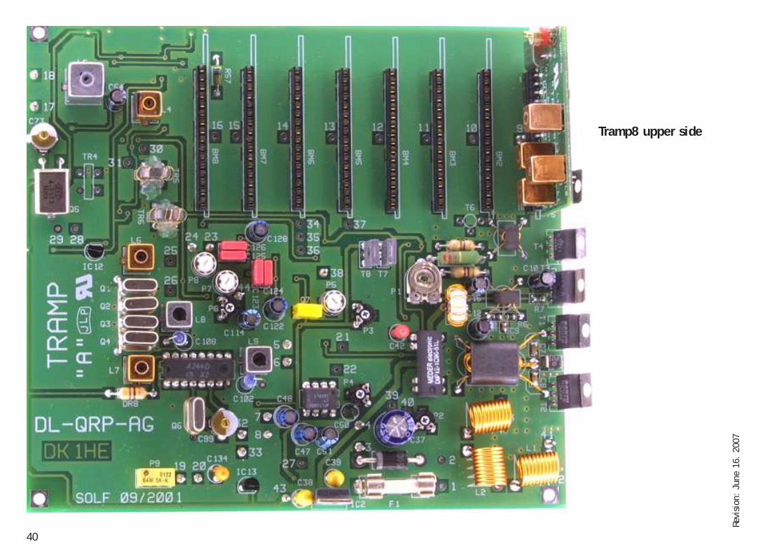
Tramp8 upper side

41
Revi
sion
: ju
ne 1
6. 2
007

Revi
sion
: Ju
ne 1
6. 2
007
42
Appendix:Very late we found, that there is a strange problem with the BandmodulVCO. The original design generates a huge amount of harmonics. This canresult in a too low amount of power on the desired frequency at the mixerinput.We found out that we drastically decrese the harmonics if we change C1 toa much higher value and R9 to a much lower value. R9 should be as low aspossible before the VCO becomes instable.Below you see the minimum values we found by experiments. As a compro-mize we ship a 2k2 R9 for all bandmoduls and the new C17 as listed sinceJan. 2005
Experimentel Values (lower values of R9 result in instable VCO)
Band C17 R9
80m: 330pF 1k840m: 220pF 1k30m: 220pF 1k220m: 220pF 1k217m: 180pF 1k815m: 150pF 1k812m: 120pF 1k10m: 100pF 1k2

43
Revi
sion
: ju
ne 1
6. 2
007

Revi
sion
: Ju
ne 1
6. 2
007
44