dual band hf cw transceiver - qrpkits.comqrpkits.com/files/dual_band_manual_rev051009.pdf · dual...
TRANSCRIPT
1
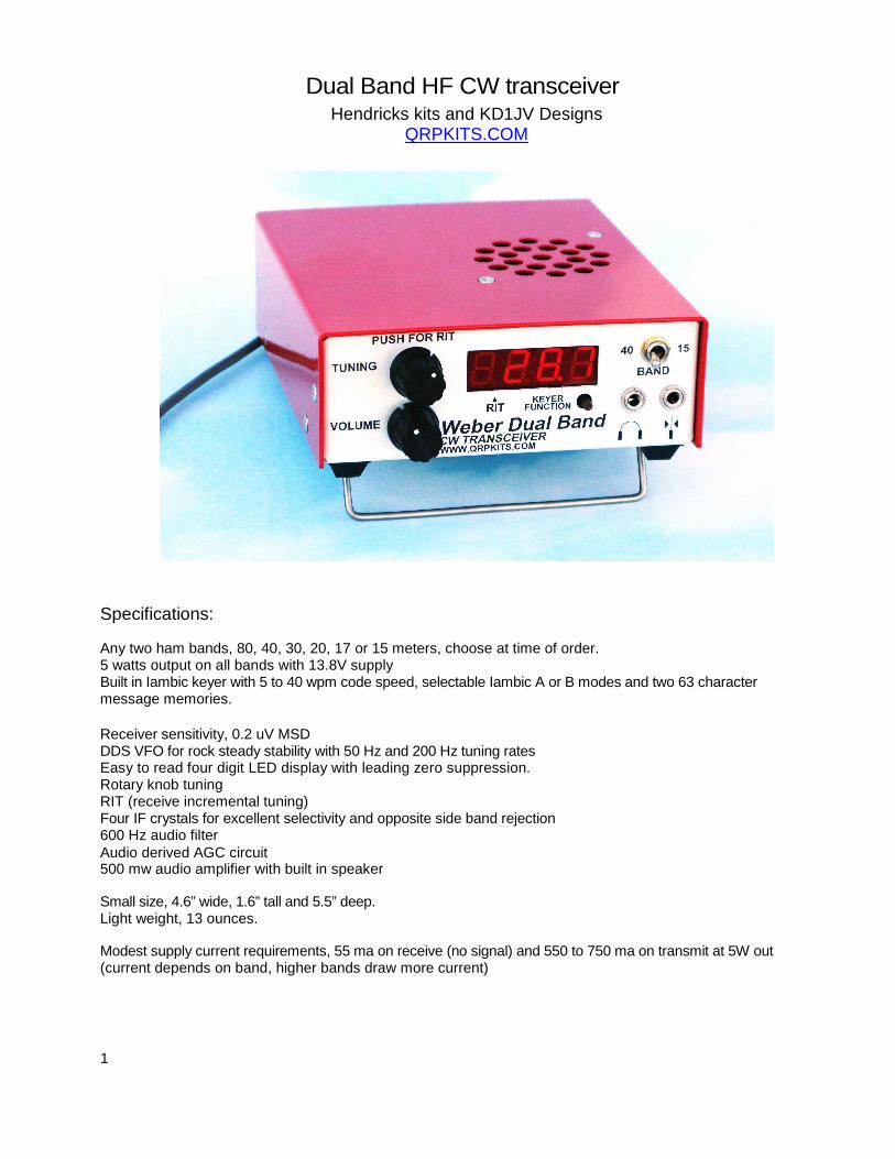
Dual Band HF CW transceiver Hendricks kits and KD1JV Designs
QRPKITS.COM
Specifications:
Any two ham bands, 80, 40, 30, 20, 17 or 15 meters, choose at time of order. 5 watts output on all bands with 13.8V supply Built in Iambic keyer with 5 to 40 wpm code speed, selectable Iambic A or B modes and two 63 character message memories.
Receiver sensitivity, 0.2 uV MSD DDS VFO for rock steady stability with 50 Hz and 200 Hz tuning rates Easy to read four digit LED display with leading zero suppression. Rotary knob tuning RIT (receive incremental tuning) Four IF crystals for excellent selectivity and opposite side band rejection 600 Hz audio filter Audio derived AGC circuit 500 mw audio amplifier with built in speaker
Small size, 4.6” wide, 1.6” tall and 5.5” deep. Light weight, 13 ounces.
Modest supply current requirements, 55 ma on receive (no signal) and 550 to 750 ma on transmit at 5W out (current depends on band, higher bands draw more current)
2
Assembly Instructions:
The quickest and easiest way to build the rig is in “layers”. The lowest profile parts are installed first, such as resistors and diodes, then higher profile parts such as capacitors and so on. Once the board is populated with all the parts, testing will be done by inserting the various Integrated Circuit chips one at a time and testing the associated stage they are used with.
Before you start assembly, it is helpful to sort the parts into types and values.
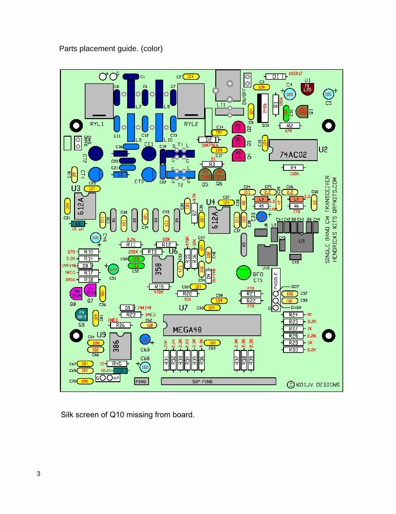
In general, parts are numbered on the board in rows, starting with the lowest part number in the upper left corner of the board (this is the back end) and then run left to right and then zig-zag down the board to the front end. Parts will be inserted in that order. Part values are marked in red on the parts placement diagram on the next page for easy reference. There are two placement diagrams included. The first is in color, which makes the various parts types stand out better, but would use a lot of ink to print out. A second, inkjet friendly diagram is also included. At least one of these diagrams should be printed out for easy reference as you build up the board.
Parts filled in with dark blue / light blue are band specific values. Refer to chart for values. SMT parts filled in with dark gray are pre-installed. Experienced builds should be able to simply sort the parts and follow the placement diagram to assemble most of the board. It is still a good idea to review all the assembly instructions in case there are some details to pay attention to.
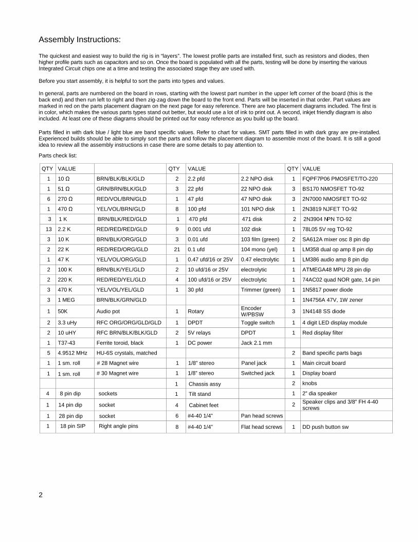
Parts check list:
QTY VALUE QTY VALUE QTY VALUE
1 10 Ω BRN/BLK/BLK/GLD 2 2.2 pfd 2.2 NPO disk 1 FQPF7P06 PMOSFET/TO-220
1 51 Ω GRN/BRN/BLK/GLD 3 22 pfd 22 NPO disk 3 BS170 NMOSFET TO-92
6 270 Ω RED/VOL/BRN/GLD 1 47 pfd 47 NPO disk 3 2N7000 NMOSFET TO-92
1 470 Ω YEL/VOL/BRN/GLD 8 100 pfd 101 NPO disk 1 2N3819 NJFET TO-92
3 1 K BRN/BLK/RED/GLD 1 470 pfd 471 disk 2 2N3904 NPN TO-92
13 2.2 K RED/RED/RED/GLD 9 0.001 ufd 102 disk 1 78L05 5V reg TO-92
3 10 K BRN/BLK/ORG/GLD 3 0.01 ufd 103 film (green) 2 SA612A mixer osc 8 pin dip
2 22 K RED/RED/ORG/GLD 21 0.1 ufd 104 mono (yel) 1 LM358 dual op amp 8 pin dip
1 47 K YEL/VOL/ORG/GLD 1 0.47 ufd/16 or 25V 0.47 electrolytic 1 LM386 audio amp 8 pin dip
2 100 K BRN/BLK/YEL/GLD 2 10 ufd/16 or 25V electrolytic 1 ATMEGA48 MPU 28 pin dip
2 220 K RED/RED/YEL/GLD 4 100 ufd/16 or 25V electrolytic 1 74AC02 quad NOR gate, 14 pin
3 470 K YEL/VOL/YEL/GLD 1 30 pfd Trimmer (green) 1 1N5817 power diode
3 1 MEG BRN/BLK/GRN/GLD 1 1N4756A 47V, 1W zener
1 50K Audio pot 1 Rotary Encoder W/PBSW 3 1N4148 SS diode
2 3.3 uHy RFC ORG/ORG/GLD/GLD 1 DPDT Toggle switch 1 4 digit LED display module
2 10 uHY RFC BRN/BLK/BLK/GLD 2 5V relays DPDT 1 Red display filter
1 T37-43 Ferrite toroid, black 1 DC power Jack 2.1 mm
5 4.9512 MHz HU-6S crystals, matched 2 Band specific parts bags
1 1 sm. roll # 28 Magnet wire 1 1/8” stereo Panel jack 1 Main circuit board
1 1/8” stereo Switched jack 1 Display board
4 8 pin dip sockets
2 knobs
1 14 pin dip socket
1 2” dia speaker
1 28 pin dip socket
2 Speaker clips and 3/8” FH 4-40 screws
screws
8 #4-40 1/4” Flat head screws 1 DD push button sw
1 1 sm. roll # 30 Magnet wire
1 18 pin SIP Right angle pins
6 #4-40 1/4” Pan head
4 Cabinet feet
1 Tilt stand
1 Chassis assy
3
Silk screen of Q10 missing from board.
Parts placement guide. (color)
4
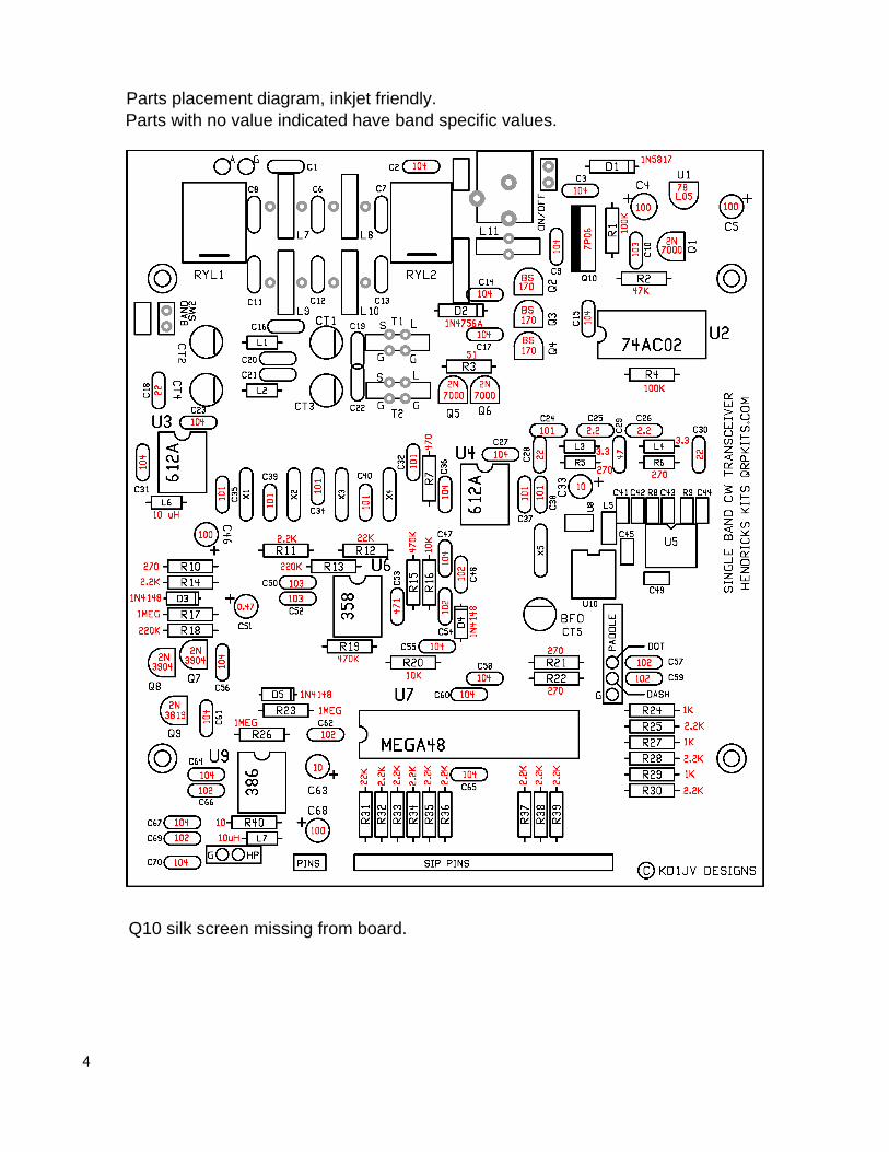
Parts placement diagram, inkjet friendly.Parts with no value indicated have band specific values.
Q10 silk screen missing from board.
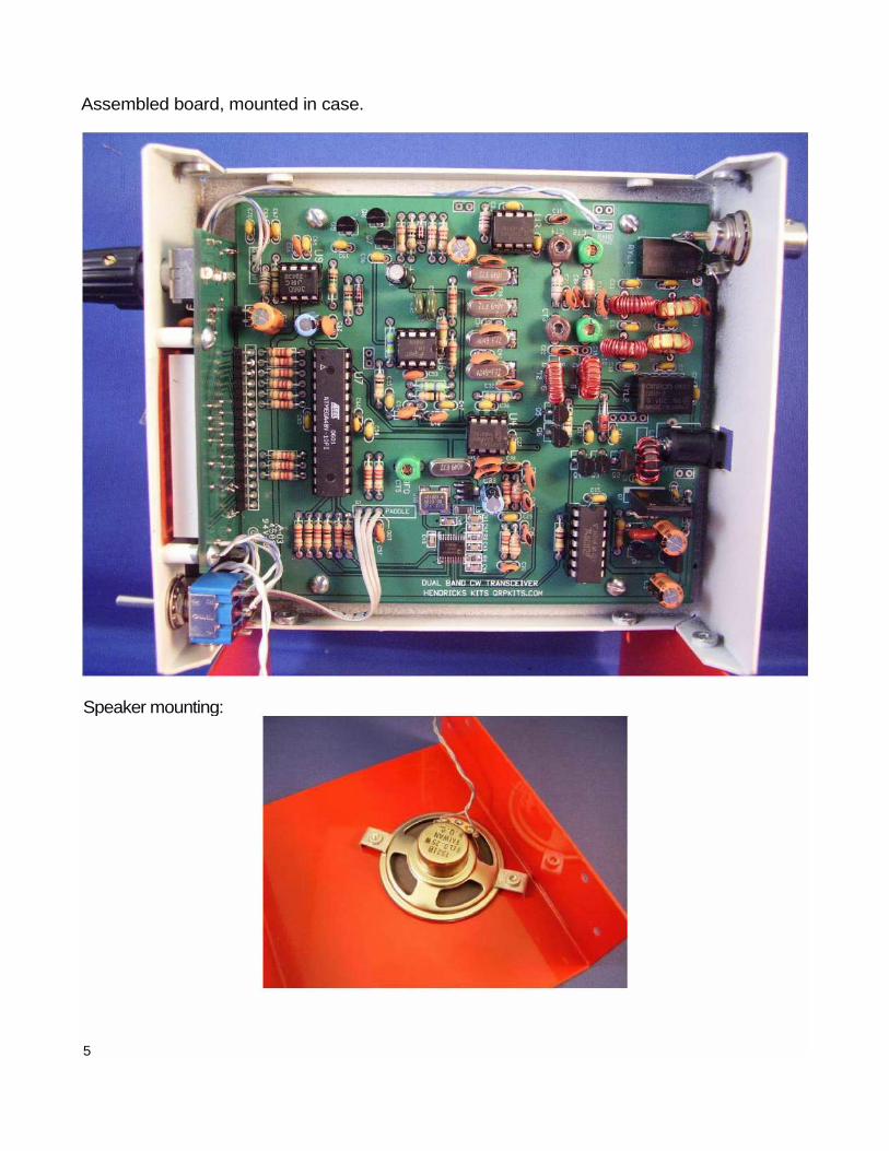
Assembled board, mounted in case.
5
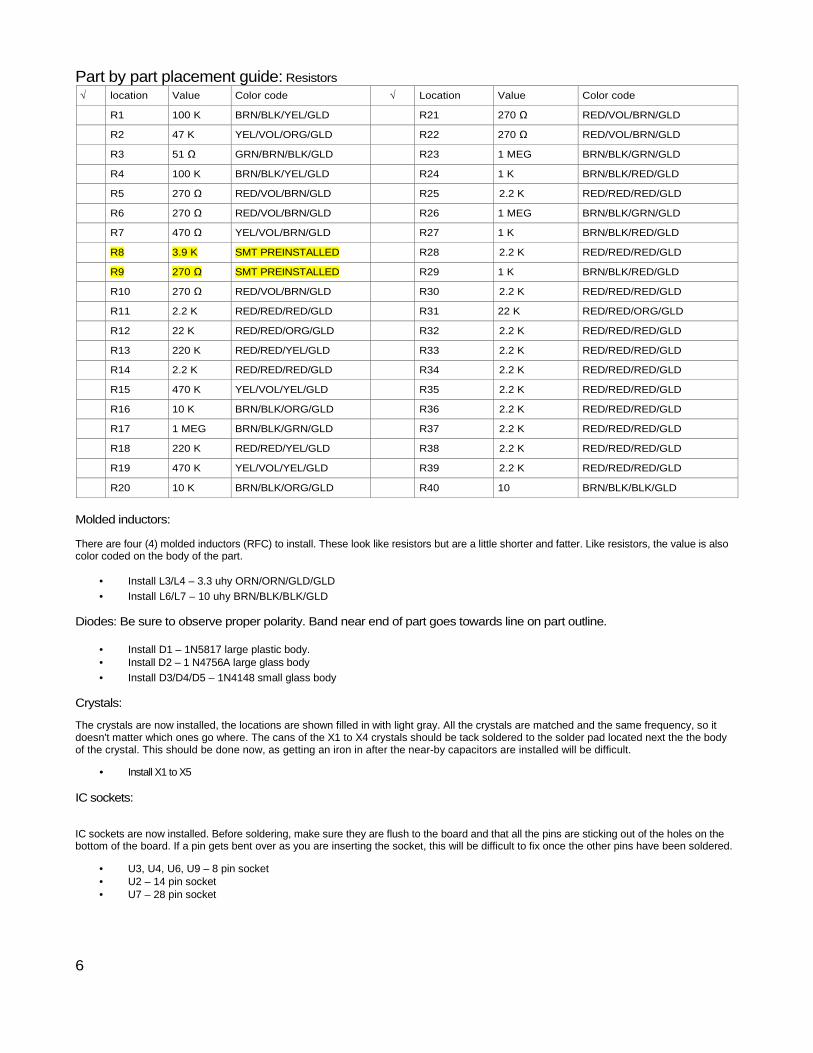
Speaker mounting:
6
Part by part placement guide: Resistors √ location Value Color code √ Location Value Color code
R1 100 K BRN/BLK/YEL/GLD R21 270 Ω RED/VOL/BRN/GLD
R2 47 K YEL/VOL/ORG/GLD R22 270 Ω RED/VOL/BRN/GLD
R3 51 Ω GRN/BRN/BLK/GLD R23 1 MEG BRN/BLK/GRN/GLD
R4 100 K BRN/BLK/YEL/GLD R24 1 K BRN/BLK/RED/GLD
R5 270 Ω RED/VOL/BRN/GLD R25 2.2 K RED/RED/RED/GLD
R6 270 Ω RED/VOL/BRN/GLD R26 1 MEG BRN/BLK/GRN/GLD
R7 470 Ω YEL/VOL/BRN/GLD R27 1 K BRN/BLK/RED/GLD
R8 3.9 K SMT PREINSTALLED R28 2.2 K RED/RED/RED/GLD
R9 270 Ω SMT PREINSTALLED R29 1 K BRN/BLK/RED/GLD
R10 270 Ω RED/VOL/BRN/GLD R30 2.2 K RED/RED/RED/GLD
R11 2.2 K RED/RED/RED/GLD R31 22 K RED/RED/ORG/GLD
R12 22 K RED/RED/ORG/GLD R32 2.2 K RED/RED/RED/GLD
R13 220 K RED/RED/YEL/GLD R33 2.2 K RED/RED/RED/GLD
R14 2.2 K RED/RED/RED/GLD R34 2.2 K RED/RED/RED/GLD
R15 470 K YEL/VOL/YEL/GLD R35 2.2 K RED/RED/RED/GLD
R16 10 K BRN/BLK/ORG/GLD R36 2.2 K RED/RED/RED/GLD
R17 1 MEG BRN/BLK/GRN/GLD R37 2.2 K RED/RED/RED/GLD
R18 220 K RED/RED/YEL/GLD R38 2.2 K RED/RED/RED/GLD
R19 470 K YEL/VOL/YEL/GLD R39 2.2 K RED/RED/RED/GLD
R20 10 K BRN/BLK/ORG/GLD R40 10 BRN/BLK/BLK/GLD
Molded inductors:
There are four (4) molded inductors (RFC) to install. These look like resistors but are a little shorter and fatter. Like resistors, the value is also color coded on the body of the part.
• Install L3/L4 – 3.3 uhy ORN/ORN/GLD/GLD • Install L6/L7 – 10 uhy BRN/BLK/BLK/GLD
Diodes: Be sure to observe proper polarity. Band near end of part goes towards line on part outline.
• Install D1 – 1N5817 large plastic body. • Install D2 – 1 N4756A large glass body • Install D3/D4/D5 – 1N4148 small glass body
Crystals:
The crystals are now installed, the locations are shown filled in with light gray. All the crystals are matched and the same frequency, so it doesn't matter which ones go where. The cans of the X1 to X4 crystals should be tack soldered to the solder pad located next the the body of the crystal. This should be done now, as getting an iron in after the near-by capacitors are installed will be difficult.
• Install X1 to X5
IC sockets:
IC sockets are now installed. Before soldering, make sure they are flush to the board and that all the pins are sticking out of the holes on the bottom of the board. If a pin gets bent over as you are inserting the socket, this will be difficult to fix once the other pins have been soldered.
• U3, U4, U6, U9 – 8 pin socket • U2 – 14 pin socket • U7 – 28 pin socket
7
Capacitors:
There are four types of capacitors used. Multi-layer (MONO) caps, which are generally yellow and rectangular is shape.
NPO type disks will have a black dot on the top edge of the cap. Note. Some of the ceramic disk caps will have lead spacing wider then the hole spacing on the board. In this case, use your needle nose pliers to kink both leads inward slightly to match the board hole spacing.
Film capacitors. These will be green in color.
Aluminum Electrolytic. These are round cylinders and have polarity. They must be installed with the correct polarity. Electrolytic caps inserted with the wrong polarity across the DC supply can heat up and explode! The negative lead is marked with a black stripe and the positive lead is always the longer lead.
Capacitor value markings:
The capacitor value is marked on the part with a two or three digit number and is read in picofards. The third digit is the zero multiplier. Values of less than 100 pfd generally show only two digits, but sometimes three. Therefore, if a part is marked 470, that means it is a 47 pfd cap and not a 470 pfd cap. A 470 pfd cap would be marked 471. Mono caps also often have letters printed on the part. These letters indicate the type or tolerance and can be disregarded.
NOTE: Although the electrolytic caps are listed in the table below, they should be installed last.
√ location value type √ location value type
C1 BAND SPEC SEE BAND TABLE C23 0.1 ufd (104) MONO, YELLOW
C2 0.1 ufd (104) MONO, YELLOW C24 100 pfd (101) NPO DISK, OR MONO YELLOW
C3 0.1 ufd (104) MONO, YELLOW C25 2.2 pfd (2.2) NPO DISK, BROWN
C4 100 ufd /16 or 25V ELECTOLYTIC C26 2.2 pfd (2.2) NPO DISK, BROWN
C5 100 ufd /16 or 25V ELECTOLYTIC C27 0.1 ufd (104) MONO, YELLOW
C6 BAND SPEC SEE BAND TABLE C28 22 pfd (22) NPO DISK, BROWN
C7 BAND SPEC SEE BAND TABLE C29 47 pfd (47) NPO DISK, BROWN
C8 BAND SPEC SEE BAND TABLE C30 22 pfd (22) NPO DISK, BROWN
C9 0.1 ufd (104) MONO, YELLOW C31 0.1 ufd (104) MONO, YELLOW
C10 0.01 ufd (103) FILM, GREEN C32 100 pfd (101) NPO DISK, OR MONO YELLOW
C11 BAND SPEC SEE BAND TABLE C33 10 ufd /16 or 25V ELECTROLYTIC
C12 BAND SPEC SEE BAND TABLE C34 100 pfd (101) NPO DISK, BROWN
C13 BAND SPEC SEE BAND TABLE C35 100 pfd (101) NPO DISK, OR MONO YELLOW
C14 0.1 ufd (104) MONO, YELLOW C36 0.1 ufd (104) MONO, YELLOW
C15 0.1 ufd (104) MONO, YELLOW C37 100 pfd (101) NPO DISK, OR MONO YELLOW
C16 BAND SPEC SEE BAND TABLE C38 100 pfd (101) NPO DISK, OR MONO YELLOW
C17 0.1 ufd (104) MONO, YELLOW C39 100 pfd (101) NPO DISK, OR MONO YELLOW
C18 22 pfd (22) DISK C40 100 pfd (101) NPO DISK, OR MONO YELLOW
C19 BAND SPEC SEE BAND TABLE C41 .1ufd SMT PREINSTALLED
C20 BAND SPEC SEE BAND TABLE C42 .01 ufd SMT PREINSTALLED
C21 BAND SPEC SEE BAND TABLE C43 .01 ufd SMT, PREINSTALLED
C22 BAND SPEC SEE BAND TABLE C44 22 pfd SMT, PREINSTALLED
C45 .01 ufd SMT, PREINSTALLED C58 0.1 ufd (104) MONO, YELLOW
C46 100 ufd/16 or 25V ELECTROLYTIC C59 .001 ufd (102) DISK, BROWN
8
C47 0.1 ufd (104) MONO, YELLOW C60 0.1 ufd (104) MONO, YELLOW
C48 .001 ufd (102) DISK, BROWN C61 0.1 ufd (104) MONO, YELLOW
C49 .01 ufd SMT, PREINSTALLED C62 .001 ufd (102) DISK, BROWN
C50 0.01 ufd (103) FILM, GREEN C63 10 ufd/16 or 25V ELECTROLYTIC
C51 0.47 ufd/16 or 25V ELECTROLYTIC C64 0.1 ufd (104) MONO, YELLOW
C52 0.01 ufd (103) FILM, GREEN C65 0.1 ufd (104) MONO, YELLOW
C53 470 pfd (471) DISK, BROWN C66 .001 ufd (102) DISK, BROWN
C54 .001 ufd (102) DISK, BROWN C67 0.1 ufd (104) MONO, YELLOW
C55 0.1 ufd (104) MONO, YELLOW C68 100 ufd/16 or,25V ELECTROLYTIC
C56 0.1 ufd (104) MONO, YELLOW C69 .001 ufd (102) DISK, BROWN
C57 .001 ufd (102) DISK, BROWN C70 0.1 ufd (104) MONO, YELLOW
• Trimmer capacitor CT5 – Green trimmer. Make use flat side of part is facing the line drawn in the circle outline on the board.
• L11 – L11 is wound with 15 turns of # 28 wire on the black T37-43 core. However, do not install L8 yet. Put it aside for now. It will be installed after the initial tests have been completed.
Transistors:
Be sure to properly ready the part number on the three legged transistors so they go in the proper place. A magnifying glass maybe helpful for this. When installing the part, look out of thin shavings of the plating on the leads which might come off as you push the legs into the holes. These can cause shorts between the leads. Space the package about 1/8” above the board – no not push real close to the board. Also, be sure to orientate the flat side of the package with the flat side of the part outline.
• Install Q2, Q3, Q4 – BS170 mosfets – these are static sensitive! • Install Q1, Q5, Q6 – 2N7000 mosfets – these are also static sensitive. • Install Q7, Q8 – 2N3904 NPN • Install Q9 – 2N3819 j-fet • Install U1 – 78L05 5V regulator • Install Q10, FQPF7P06 – line up the long side with the black rectangle on the board outline. Note: Q10 is labeled
Q7 on circuit board.
• Now install all the Electrolytic capacitors. Be sure to observe proper polarity. Long lead is plus side. Black stripe on the body of the can indicates negative side. C5 can explode if installed backwards!
C4, C5, C46, C68 100 ufd/16 or 25V
C33, C63 10 ufd/16 or 25V
C51 0.47 ufd/16 or 25V
DC power jack relays and the right angle SIP pin strips.
• Install DC power jack • Install the two relays, RYL1 and RYL2. Note the line on one end of the relay and match this with the line on the relay
outline. • Install right angle SIP pin strips. You will need to cut 2 pins from the strip, as these two pins are offset from the rest of
the pins to the left. Simply snip the plastic between the pins with your side cutters. Insert the short pins into the main board. The pins will not quite stick all the way through the board, so make sure the pins are well seated. DO NOT SOLDER the pins to the board yet. Do this after trial fitting the main board with the display board attached into the cabinet.
9
Band specific parts:
In the color parts layout, the transmitter low pass filter and associated receiver input parts are filled in with the same color. Band “A” parts are colored in light blue and Band “B” is colored in dark blue . It doesn't matter which specific band you call “A” and which you call “B”, that will be programmed later. Just note which one is which. Keep in mind that since the relays are non-latching, a small amount of additional current will be drawn by the rig when band “B” is selected, so you might want to put the band you think will be used most often as band “A”. Part locations are indicated in the table for band “A” first, then band “B”.
Be sure to count the turns on L7/L8/L9 and L1 0 properly. Each time the wire passes through the center of the core, this is one turn. Having one extra turn, which is a common mistake, will result in reduced power output. Also the turns should be reasonably tight to the core. Sloppy winding can result in reduced performance. Evenly space the turns around the core.
Winding T1/T2: See next page for instruction on winding T1/T2 so leads end up in proper locations for the outline.
80 meters Value Type 40 meters Value Type
C16 or C1 100 pfd 101 NPO Disk C16 or C1 68 pfd NPO disk
C11 or C8 680 pfd 681 mono C0G C11 or C8 330 pfd (331) C0G
C12 or C6 1500 pfd 152 mono C0G C12 or C6 680 pfd (681) C0G
C13 or C7 680 pfd 681 mono C0G C13 or C7 330 pfd (331) C0G
C22 or C19 68 pfd 68 NPO Disk C22 or C19 47 pfd disk
C21 or C20 15 pfd 15 NPO Disk C21 or C20 10 pfd NPO disk
CT3 or CT4, CT1 or CT2
70 pfd Brown trimmer CT3 or CT4, CT1 or CT2
70 pfd trimmer Brown
L10 or L8 24 turns #30 wire T37-2 Red L10 or L8 18 turns #28 wire T37-2 Red
L9 or L7 29 turns #30 wire T37-2 Red L9 or L7 20 turns #28 wire T37-2 Red
L2 or L1 18 uHy BRN/GRY/BLK/GLD L2 or L1 8.2 uHy GRY/RED/GLD/GLD
T1 or T2 60 turns/ 6 turns #32 wire T37-2 Red T1 or T2 45 turns / 4 turns #30 wire T37-2 Red
30 meters 20 meters C16 or C1 47 pfd 47 NPO Disk C16 or C1 22 pfd 22 NPO Disk
C11 or C8 220 pfd 221 mono C0G C11 or C8 150 151 mono C0G
C12 or C6 560 pfd 561 mono C0G C12 or C6 330 331 mono C0G
C13 or C7 220 pfd 221 mono C0G C13 or C7 150 151 mono C0G
C22 or C19 4.7 pfd 4.7 NPO Disk C22 or C19 2.2 pfd 2.2 NPO Disk
C21 or C20 None C21 or C20 None CT3 or CT4, CT1 or CT2
30 pfd Green trimmer CT3 or CT4, CT1 or CT2
30 pfd Green trimmer
L10 or L8 13 turns #28 wire T37-2 Red L10 or L8 13 turns # 28 wire T37-6 Yellow
L9 or L7 16 turns #28 wire T37-2 Red L9 or L7 16 turns #28 wire T37-6 Yellow
L2 or L1 8.2 uHy GRY/RED/GLD/GLD L2 or L1 5.6 uHy GRN/BLU/GLD/GLD
T1 or T2 45 turns / 4 truns # 30 wire T37-2 Red T1 or T2 38 turns / 4 turns # 30 wire T37-2 Red
17 meters 15 meters C16 or C1 15 pfd 15 NPO disk C16 or C1 15 pfd 15 NPO disk
C11 or C8 47 pfd 47 mono C0G C11 or C8 47 pfd 47 mono C0G
C12 or C6 220 pfd 221 mono C0G C12 or C6 220 pfd 221 mono C0G
C13 or C7 100 pfd 101 Disk C13 or C7 100 pfd 101 Disk
C22 or C19 none C22 or C19 none C21 or C20 2.2 pdf 2.2 NPO Disk C21 or C20 2.2 pfd 2.2 NPO Disk
CT3 or CT4, CT1 or CT2
30 pfd Green trimmer CT3 or CT4, CT1 or CT2
30 pfd Green trimmer
L10 or L8 13 turns # 28 wire T37-6 Yellow L10 or L8 11 turns #28 wire T37-6 yellow
L9 or L7 16 turns # 28 wire T37-6 Yellow L9 or L7 14 turns #28 wire T37-6 yellow
L2 or L1 3.3 uHy ORG/ORG/GLD/GLD L2 or L1 3.3 uHy ORG/ORG/GLD/GLD
T1 or T2 25 Turns/ 4 Turns #30 wire T37-2 RED T1 or T2 25 Turns/ 4 Turns #30 wire T37-2 RED
1 0
T1/T2 winding: Hold the core in your left hand and start winding by passing 1/2” of the magnet wire up through the “bottom” side of the core as shown in the diagram. Then continue winding the remaining required number of turns by passing the long end of the wire in and down from the top of the core. When you get to the end of the required number of secondary turns, make about a 1/2” loop and continue winding the four link turns.
Snip the loop to separate the secondary (S) from the link (L) winding, then tin the wires. Insert the core into the board and solder. It will not matter along which side of the board outline the wide side of the core faces.
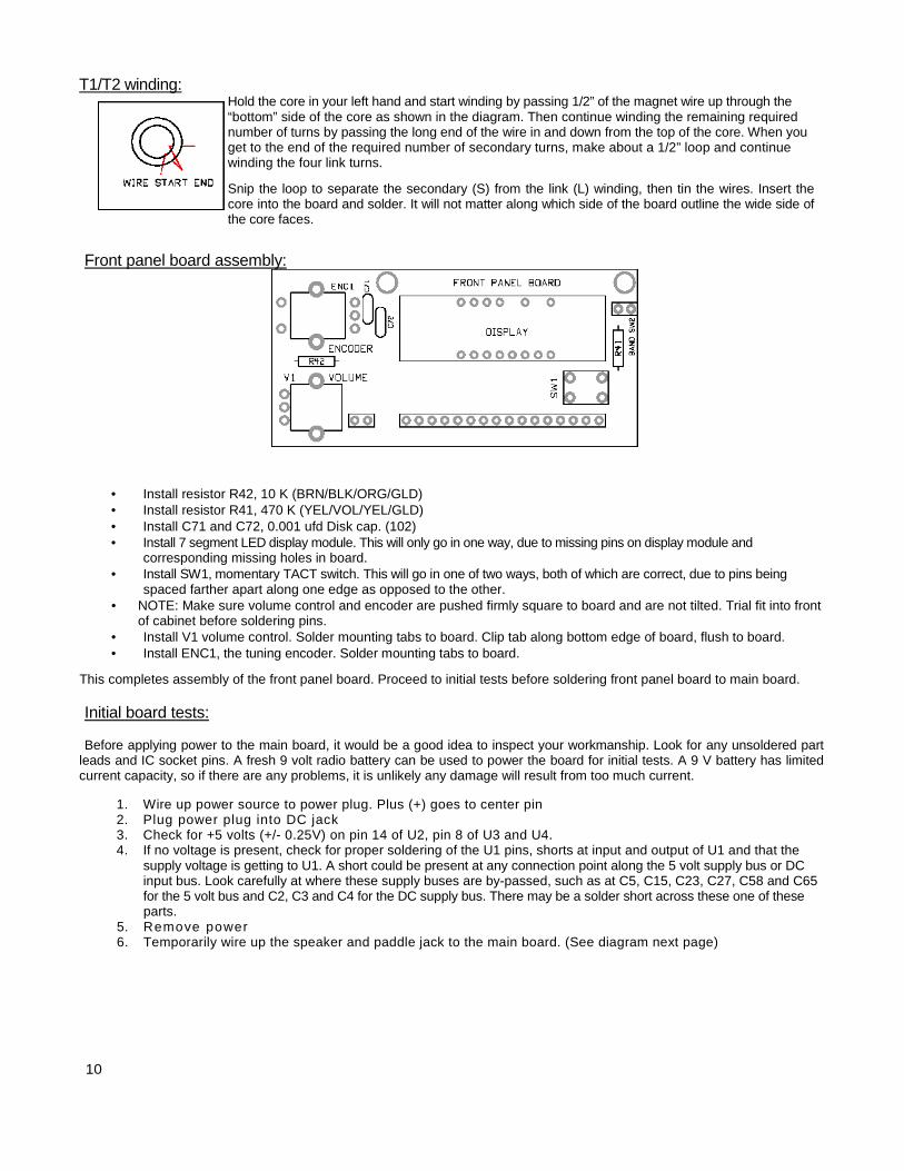
Front panel board assembly:
• Install resistor R42, 10 K (BRN/BLK/ORG/GLD) • Install resistor R41, 470 K (YEL/VOL/YEL/GLD) • Install C71 and C72, 0.001 ufd Disk cap. (102) • Install 7 segment LED display module. This will only go in one way, due to missing pins on display module and
corresponding missing holes in board. • Install SW1, momentary TACT switch. This will go in one of two ways, both of which are correct, due to pins being
spaced farther apart along one edge as opposed to the other. • NOTE: Make sure volume control and encoder are pushed firmly square to board and are not tilted. Trial fit into front
of cabinet before soldering pins. • Install V1 volume control. Solder mounting tabs to board. Clip tab along bottom edge of board, flush to board. • Install ENC1, the tuning encoder. Solder mounting tabs to board.
This completes assembly of the front panel board. Proceed to initial tests before soldering front panel board to main board.
Initial board tests:
Before applying power to the main board, it would be a good idea to inspect your workmanship. Look for any unsoldered part leads and IC socket pins. A fresh 9 volt radio battery can be used to power the board for initial tests. A 9 V battery has limited current capacity, so if there are any problems, it is unlikely any damage will result from too much current.
1. Wire up power source to power plug. Plus (+) goes to center pin 2. Plug power plug into DC jack 3. Check for +5 volts (+/- 0.25V) on pin 14 of U2, pin 8 of U3 and U4. 4. If no voltage is present, check for proper soldering of the U1 pins, shorts at input and output of U1 and that the
supply voltage is getting to U1. A short could be present at any connection point along the 5 volt supply bus or DC input bus. Look carefully at where these supply buses are by-passed, such as at C5, C15, C23, C27, C58 and C65 for the 5 volt bus and C2, C3 and C4 for the DC supply bus. There may be a solder short across these one of these parts.
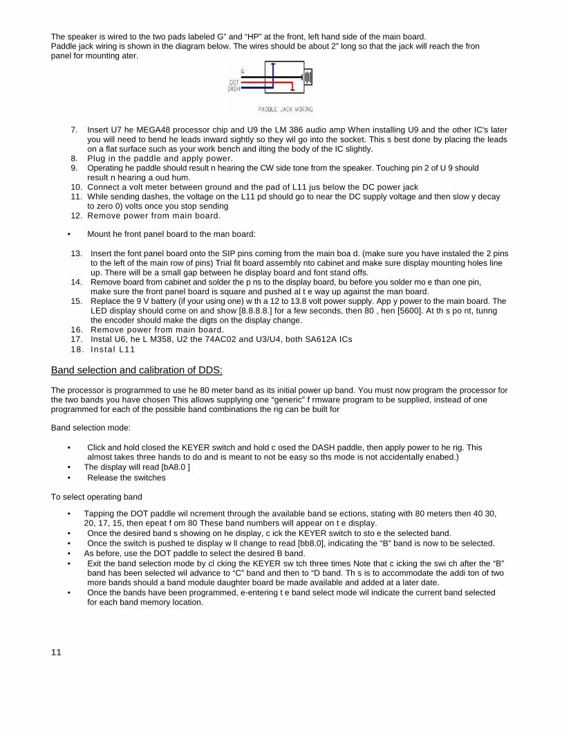
5. Remove power 6. Temporarily wire up the speaker and paddle jack to the main board. (See diagram next page)
11
The speaker is wired to the two pads labeled G” and “HP” at the front, left hand side of the main board. Paddle jack wiring is shown in the diagram below. The wires should be about 2” long so that the jack will reach the fron panel for mounting ater.
7. Insert U7 he MEGA48 processor chip and U9 the LM 386 audio amp When installing U9 and the other IC's later you will need to bend he leads inward sightly so they wil go into the socket. This s best done by placing the leads on a flat surface such as your work bench and ilting the body of the IC slightly.
8. Plug in the paddle and apply power. 9. Operating he paddle should result n hearing the CW side tone from the speaker. Touching pin 2 of U 9 should
result n hearing a oud hum. 10. Connect a volt meter between ground and the pad of L11 jus below the DC power jack 11. While sending dashes, the voltage on the L11 pd should go to near the DC supply voltage and then slow y decay
to zero 0) volts once you stop sending 12. Remove power from main board.
• Mount he front panel board to the man board:
13. Insert the font panel board onto the SIP pins coming from the main boa d. (make sure you have instaled the 2 pins to the left of the main row of pins) Trial fit board assembly nto cabinet and make sure display mounting holes line up. There will be a small gap between he display board and font stand offs.
14. Remove board from cabinet and solder the p ns to the display board, bu before you solder mo e than one pin, make sure the front panel board is square and pushed al t e way up against the man board.
15. Replace the 9 V battery (if your using one) w th a 12 to 13.8 volt power supply. App y power to the main board. The LED display should come on and show [8.8.8.8.] for a few seconds, then 80 , hen [5600]. At th s po nt, tunng the encoder should make the digts on the display change.
16. Remove power from main board. 17. Instal U6, he L M358, U2 the 74AC02 and U3/U4, both SA612A ICs 18. Ins ta l L11
Band selection and calibration of DDS:
The processor is programmed to use he 80 meter band as its initial power up band. You must now program the processor for the two bands you have chosen This allows supplying one “generic” f rmware program to be supplied, instead of one programmed for each of the possible band combinations the rig can be built for
Band selection mode:
• Click and hold closed the KEYER switch and hold c osed the DASH paddle, then apply power to he rig. This almost takes three hands to do and is meant to not be easy so ths mode is not accidentally enabed.)
• The display will read [bA8.0 ] • Release the switches
To select operating band
• Tapping the DOT paddle wil ncrement through the available band se ections, stating with 80 meters then 40 30, 20, 17, 15, then epeat f om 80 These band numbers will appear on t e display.
• Once the desired band s showing on he display, c ick the KEYER switch to sto e the selected band. • Once the switch is pushed te display w ll change to read [bb8.0], indicating the “B” band is now to be selected. • As before, use the DOT paddle to select the desired B band. • Exit the band selection mode by cl cking the KEYER sw tch three times Note that c icking the swi ch after the “B”
band has been selected wil advance to “C” band and then to “D band. Th s is to accommodate the addi ton of two more bands should a band module daughter board be made available and added at a later date.
• Once the bands have been programmed, e-entering t e band select mode wil indicate the current band selected for each band memory location.
12
Calibration of DDS reference frequency and LO frequency:
Calibration of the reference frequency and LO frequency is not absolutely necessary, but will improve the performance of the rig. If an accurate frequency counter and audio oscilloscope , either CRT or PC based, is not available, do not attempt calibration. Calibration can be done at a later time. To enter the calibration mode, first power down the board if it is on. Then, while holding closed the KEYER switch and the DOT paddle closed, apply power to the board. The display will read [CAL.r] and release the switches.
• In the “CAL.r” mode, the DDS is producing about a 10.000,000 MHz signal. A counter can be placed at Pin 4 of the U2 socket to read this frequency. The paddle is then used to adjust the signal so that it is exactly 10.000,000 MHz. Tapping the dot paddle will increment the frequency up, while the dash paddle will increment it down.
• Once the frequency is adjusted to 10.000,000 MHz, click the “Keyer” switch to advance to the LO cal mode.
• The display will now read “CAL.O” and the LO frequency can now be tweaked.
• This adjustment is used to center the LO frequency into the pass band of the crystal filter, which might vary a little depending on the exact frequency of the crystals used in the filter. All the crystals are matched to the same frequency, but exactly where the center frequency falls can vary from crystal lot to lot.
• Pre-set the BFO trimmer to about 1/4 turn from its factory setting. 180 degrees or 1/2 turn changes the setting from maximum to minimum capacitance.
• Connect an Oscilloscope to pin 7 of U5, the LM358 IC.
• Use the paddles again to tune the LO frequency through the pass band of the crystal filter. Observe the points at which the amplitude of the signal starts to fall off on either side of the pass band. You will likely see a peak in the signal on each side of the pass band, just before it starts to quickly roll off. You will want to set the LO frequency about mid way between these two peaks.
• Once the LO frequency is set, move the Oscilloscope to pin 1 of U5.
• Now adjust the BFO trimmer to peak the amplitude of the signal. This will center the BFO note into the center of the pass band of the audio filter stage.
• Click the “KEYER” switch to finish up the calibration. The processor will reset, load the new values and the rig is almost ready to operate.
Please note that each time the calibration procedure is enabled, the default operating values are loaded as a starting point. This is done in the remote chance the calibration data stored in EEPROM has become corrupted and known good starting values are used.
Final assembly into case:
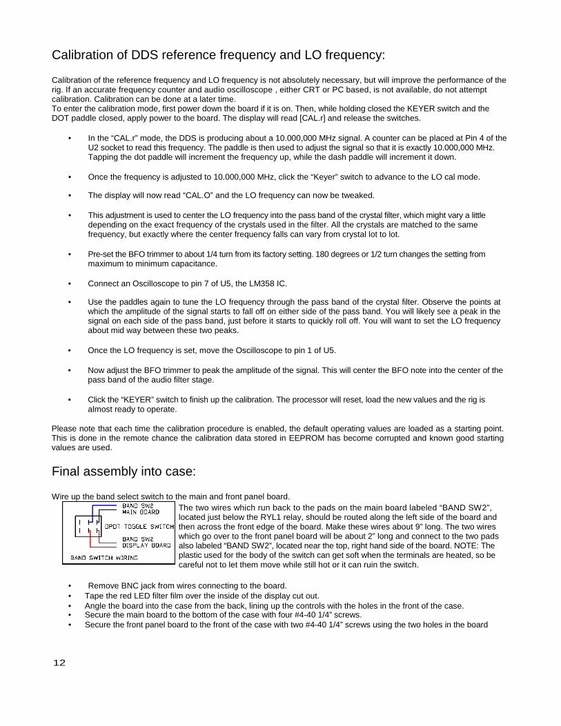
Wire up the band select switch to the main and front panel board. The two wires which run back to the pads on the main board labeled “BAND SW2”, located just below the RYL1 relay, should be routed along the left side of the board and then across the front edge of the board. Make these wires about 9” long. The two wires which go over to the front panel board will be about 2” long and connect to the two pads also labeled “BAND SW2”, located near the top, right hand side of the board. NOTE: The plastic used for the body of the switch can get soft when the terminals are heated, so be careful not to let them move while still hot or it can ruin the switch.
• Remove BNC jack from wires connecting to the board. • Tape the red LED filter film over the inside of the display cut out. • Angle the board into the case from the back, lining up the controls with the holes in the front of the case. • Secure the main board to the bottom of the case with four #4-40 1/4” screws. • Secure the front panel board to the front of the case with two #4-40 1/4” screws using the two holes in the board
13
along the top edge of the board on either side of the display. • Install the BNC jack and connect to the wires from the main board. HINT: To keep the BNC jack from spinning as
you tighten the nut, put a BNC plug on the jack and hold that firmly. • Install the paddle jack into the cabinet front panel hole.
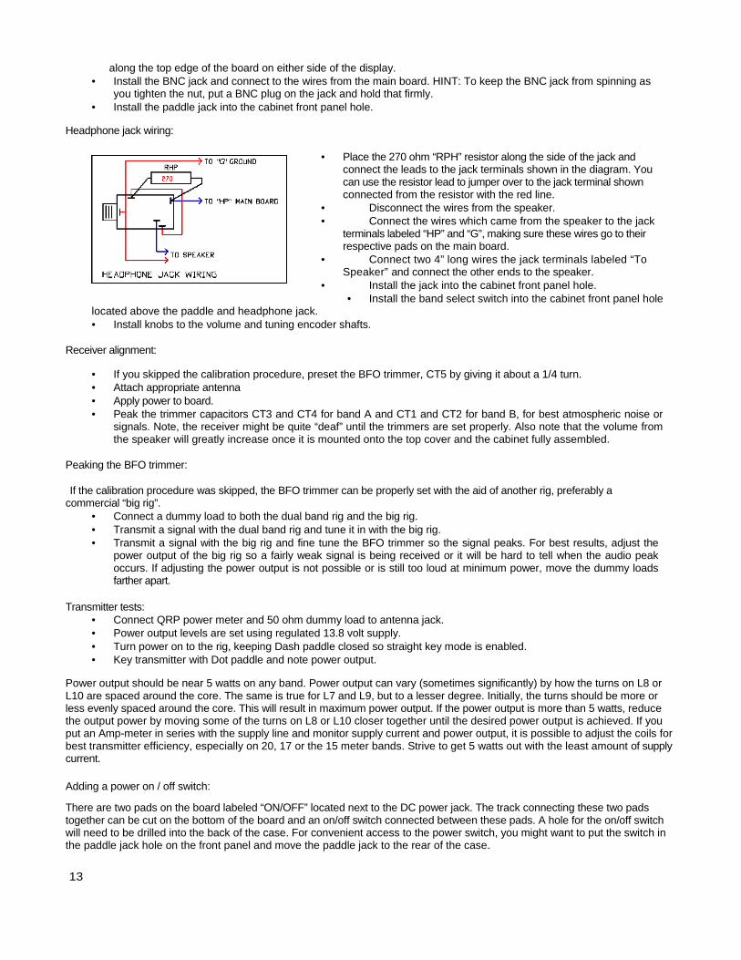
Headphone jack wiring:
• Place the 270 ohm “RPH” resistor along the side of the jack and connect the leads to the jack terminals shown in the diagram. You can use the resistor lead to jumper over to the jack terminal shown connected from the resistor with the red line.
• Disconnect the wires from the speaker. • Connect the wires which came from the speaker to the jack
terminals labeled “HP” and “G”, making sure these wires go to their respective pads on the main board.
• Connect two 4” long wires the jack terminals labeled “To Speaker” and connect the other ends to the speaker.
• Install the jack into the cabinet front panel hole. • Install the band select switch into the cabinet front panel hole
located above the paddle and headphone jack. • Install knobs to the volume and tuning encoder shafts.
Receiver alignment:
• If you skipped the calibration procedure, preset the BFO trimmer, CT5 by giving it about a 1/4 turn. • Attach appropriate antenna • Apply power to board. • Peak the trimmer capacitors CT3 and CT4 for band A and CT1 and CT2 for band B, for best atmospheric noise or
signals. Note, the receiver might be quite “deaf” until the trimmers are set properly. Also note that the volume from the speaker will greatly increase once it is mounted onto the top cover and the cabinet fully assembled.
Peaking the BFO trimmer:
If the calibration procedure was skipped, the BFO trimmer can be properly set with the aid of another rig, preferably a commercial “big rig”.
• Connect a dummy load to both the dual band rig and the big rig. • Transmit a signal with the dual band rig and tune it in with the big rig. • Transmit a signal with the big rig and fine tune the BFO trimmer so the signal peaks. For best results, adjust the
power output of the big rig so a fairly weak signal is being received or it will be hard to tell when the audio peak occurs. If adjusting the power output is not possible or is still too loud at minimum power, move the dummy loads farther apart.
Transmitter tests: • Connect QRP power meter and 50 ohm dummy load to antenna jack. • Power output levels are set using regulated 13.8 volt supply. • Turn power on to the rig, keeping Dash paddle closed so straight key mode is enabled. • Key transmitter with Dot paddle and note power output.
Power output should be near 5 watts on any band. Power output can vary (sometimes significantly) by how the turns on L8 or L10 are spaced around the core. The same is true for L7 and L9, but to a lesser degree. Initially, the turns should be more or less evenly spaced around the core. This will result in maximum power output. If the power output is more than 5 watts, reduce the output power by moving some of the turns on L8 or L10 closer together until the desired power output is achieved. If you put an Amp-meter in series with the supply line and monitor supply current and power output, it is possible to adjust the coils for best transmitter efficiency, especially on 20, 17 or the 15 meter bands. Strive to get 5 watts out with the least amount of supply current.
Adding a power on / off switch:
There are two pads on the board labeled “ON/OFF” located next to the DC power jack. The track connecting these two pads together can be cut on the bottom of the board and an on/off switch connected between these pads. A hole for the on/off switch will need to be drilled into the back of the case. For convenient access to the power switch, you might want to put the switch in the paddle jack hole on the front panel and move the paddle jack to the rear of the case.
14
Trouble shooting guide:
In most cases, any problems with the getting the rig to work will be tracked down to soldering problems or miss placed parts. A close visual inspection of the board is often enough to find soldering problems or the miss-placed parts.
Soldering problems fall into four groups: 1. Missing solder connections 2. Solder bridges between closely spaced pads which should not be connected togther. 3. Solder which stuck to the part lead but did not flow into the solder pad on the board. This is often caused by not using enough
heat or not placing the iron tip on both the lead and the solder pad. 4. Not making connection to the wires on the toroid coils. Even if you pre-tined the magnet wire, you may have pulled it past the
tinning when inserting the wires into the board and are not making a connection. Buzz out the connection to ensure continuity.
Miss-placed parts:
The most common error here is not reading the resistor color code correctly. Some values have identical colors, but in a different order. It is easy to mistake a 51 ohm resistor (Green/Brown/Black) for a 1 Meg resistor (Brown/Black/Green)
Trouble shooting technique:
The trick to trouble shooting is being able to narrow down the area to look at to find the problem. Just using a DVM will be sufficient for basic trouble shooting. For more difficult cases, an Oscilloscope and signal generator may be needed to track signals through the circuits.
In any case, one should first determine which parts of the circuit are working properly and this will lead you to what is not. If the rig is completely dead, the problem is likely with the power supply and could very well be a short to ground somewhere on the 5 volt supply feeding most of the IC's. If the display comes on, the microprocessor is working and if you get side tone when you use the paddle, or hear hiss when the volume control is turned all the way up, the audio amp is working. If there is no side tone or hiss, the problem maybe a simple as the wiring to the speaker/headphone jack or it might in the audio amp area.
If you get audio, but can not hear any off air signals, the problem is more difficult to find as it could be anywhere between the antenna jack and the audio amp. In this case having a signal generator and Oscilloscope are of great help in tracing the signal though the circuits.
Transmitter:
There is not a whole lot which can go wrong with the transmitter portion. Check for PA keying voltage coming out of Q10, proper soldering of the toroid magnet wire.
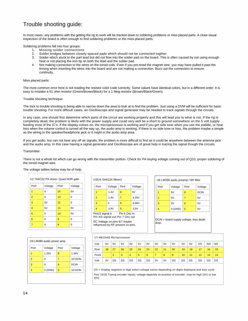
The voltage tables below may be of help.
U7 MEGA48 Microprocessor
Volt 5V 5V 5V 0V 5V 0V 0V 5V 5V 5V 5V DS 5/0 5/0
Pin# 28 27 26 25 24 23 22 21 20 19 18 17 16 15
Pin#1 2 3 4 5 6 7 8 9 10 11 12 13 14
Volt 0V DS DS DS DS DS 5V 0V DS DS DS DS DS DS
DS = Display segment or digit select voltage varies depending on digits displayed and duty cycle.
Pins 15/16 Tuning encoder inputs, voltage depends on position of encoder, may be high (5V) or low (0V)
U2 74AC02 PA driver, Quad NOR gate
Pin# Voltage Pin# Voltage
1 0 14 5V
2 0 13 0
3 5V 12 0
4 5V 11 5V
5 0 10 5V
6 0 9 0
7 0 8 0
U3/U4 SA612A Mixers
Pin# Voltage Pin# Voltage
1 1.4V 8 5V
2 1.4V 7 4.25V
3 0 6 4.96V
4 3.9V 5 3.9V Pin1/2 signal in Pin 6 Osc in Pin 4/5 signal out Pin 7 Osc out
DC Voltage on pins 6/7 maybe influenced by RF present on pins.
U6 LM358 audio preamp / BP filter
Pin# Voltage Pin# Voltage
1 5V 8 DCIN
2 5V 7 5V
3 5V 6 5V
4 0 (GND) 5 5V
DCIN = board supply voltage, less diode drop.
U9 LM386 audio power amp
Pin# Voltage Pin# Voltage
1 1.33V 8 1.34V
2 0 7 1/2 DCIN
3 0 6 DCIN
4 0 (GND) 5 1/2 DCIN
15
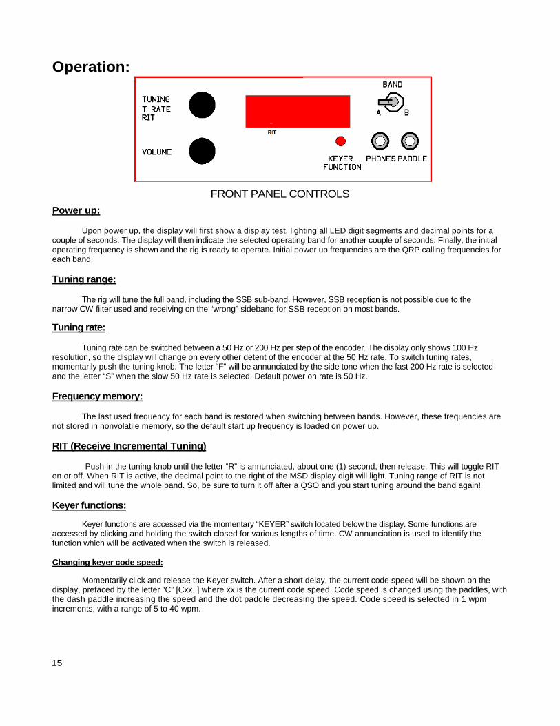
Operation:
FRONT PANEL CONTROLS
Power up:
Upon power up, the display will first show a display test, lighting all LED digit segments and decimal points for a couple of seconds. The display will then indicate the selected operating band for another couple of seconds. Finally, the initial operating frequency is shown and the rig is ready to operate. Initial power up frequencies are the QRP calling frequencies for each band.
Tuning range:
The rig will tune the full band, including the SSB sub-band. However, SSB reception is not possible due to the narrow CW filter used and receiving on the “wrong” sideband for SSB reception on most bands.
Tuning rate:
Tuning rate can be switched between a 50 Hz or 200 Hz per step of the encoder. The display only shows 100 Hz resolution, so the display will change on every other detent of the encoder at the 50 Hz rate. To switch tuning rates, momentarily push the tuning knob. The letter “F” will be annunciated by the side tone when the fast 200 Hz rate is selected and the letter “S” when the slow 50 Hz rate is selected. Default power on rate is 50 Hz.
Frequency memory:
The last used frequency for each band is restored when switching between bands. However, these frequencies are not stored in nonvolatile memory, so the default start up frequency is loaded on power up.
RIT (Receive Incremental Tuning)
Push in the tuning knob until the letter “R” is annunciated, about one (1) second, then release. This will toggle RIT on or off. When RIT is active, the decimal point to the right of the MSD display digit will light. Tuning range of RIT is not limited and will tune the whole band. So, be sure to turn it off after a QSO and you start tuning around the band again!
Keyer functions:
Keyer functions are accessed via the momentary “KEYER” switch located below the display. Some functions are accessed by clicking and holding the switch closed for various lengths of time. CW annunciation is used to identify the function which will be activated when the switch is released.
Changing keyer code speed:
Momentarily click and release the Keyer switch. After a short delay, the current code speed will be shown on the display, prefaced by the letter “C” [Cxx. ] where xx is the current code speed. Code speed is changed using the paddles, with the dash paddle increasing the speed and the dot paddle decreasing the speed. Code speed is selected in 1 wpm increments, with a range of 5 to 40 wpm.
16
Tune Up Mode:
Clicking and holding closed the keyer switch for 1 second will access the “Tune Up Mode” function. Release the switch after the side tone annunciates the Morse letter “T” to activate this function. A character resembling a “t” will appear on the display to indicate this mode is active. The dot or dash paddle can now be used to key the transmitter on and off. Click the Keyer switch again to exit this function and return to normal operation. This function is primarily used if you have an Autotuner, which requires a steady carrier for a minute or so to find a match. When using a manual antenna tuner, you would be better off sending a string of dots or dashes to reduce strain on the transmitter.
Entering messages into keyer memory:
Two, 63 character message memories are available. To enter this function, click and hold the keyer switch closed until the Morse letter “M” is annunciated by the side tone and release the switch. The display will blank to indicate it is not in normal operating mode.
Now key in your message. Ideal letter and word space timing is used to add letter group and word spacing. Therefore, if you tend to run your letters and words together, the message may come out garbled. It can take some practice and a few tries to get the message entered correctly.
Once you have completed entering the message, click the KEYER switch. The message will repeat via the side tone so you can check it's accuracy. If you need to re-enter the message, click the KEYER switch again and the Morse characters “EM” will be annunciated and you can start again.
Once the message has been keyed in correctly, tap the DOT paddle to store the message in location 1 or the Dash paddle to store in location 2. The characters “MS” be annunciated to indicate the message was stored and the frequency display will be restored.
Sending a message:
Click the KEYER switch, then within one (1) second, tap the DOT or Dash paddle to send either message 1 or 2.
Stopping or pausing the sending of a message:
Once a message has started sending, it can be terminated by holding closed the Dot paddle. Closing the DASH paddle will pause the message and continue sending from the point at which is was paused when the paddle is released. The paddle is sensed during word or letter spaces, so it has to be held closed until one of these occurs.
Straight key mode:
Straight key mode is automatically enabled if a monaural phone plug is used in the paddle jack at the time the rig is turned on. This grounds the Dash input and tells the rig to go into straight key mode. This mode can also be enabled by keeping the Dash paddle closed on power up.
Note: In straight key mode, none of the KEYER switch functions will be available, since these all require the Dash input to be active. However, you can still used the Message 1 memory if a message has been stored, but it will send at the default keyer speed of 20 wpm.
Paddle plug wiring:
Standard paddle plug wiring is used, Tip = dot, Ring = dash. Paddle sense is not programmable.
Setting keyer Iambic A or B mode:
The default Iambic mode is A mode. This can be switched to B mode by holding closed the KEYER switch for three (3) seconds. After the keyer memory function letter “M” has been annunciated, the next function will be the toggling of the Iambic mode. If A is currently enabled, B will be toggled on and the letter “B” will be annunciated and the display will show [b . ]. Conversely, if B is currently enabled, the letter “A” will be annunciated and the display will show [A .] for a second and then escape to normal operation.
The difference between A and B modes:
When using Iambic keying, holding closed both paddles will alternately send dots and dashes, with the first element being
17
determined by which paddle was closed first. The difference between A and B modes is what happens after the paddles are released. In A mode, the keyer simply stops sending. In B mode, an extra and opposite element is sent from the last element being sent when the paddles are released. The “both paddles closed” condition is sensed at the end of an inter-element space. This helps ensure that when sending a simple two element letter like “A” or “N”, an extra dot or dash isn't tacked on the end. Therefore, to send a letter such as “C”, the paddles would be released as the second dash is being sent and the final dot will automatically added. B mode is only useful for aiding in the sending of a couple of letters and can be more trouble than its worth, as your timing has to be very good.
AGC action:
The AGC is audio derived and kicks in when a fairly strong signal is received. There maybe a slight popping noise as the AGC kicks in with very strong signals, as it takes a few audio cycles to activate. The main purpose of the AGC is to keep strong signals from “blowing your ears out” and reduces the need to ride the volume control when tuning across the band.
Power supply:
The power supply voltage to the rig should be no more than 13.8 volts and no less then 10.5 volts. It is strongly recommended that a fused power cord be used between the rig and power supply with a 1 amp, fast blow fuse.
18
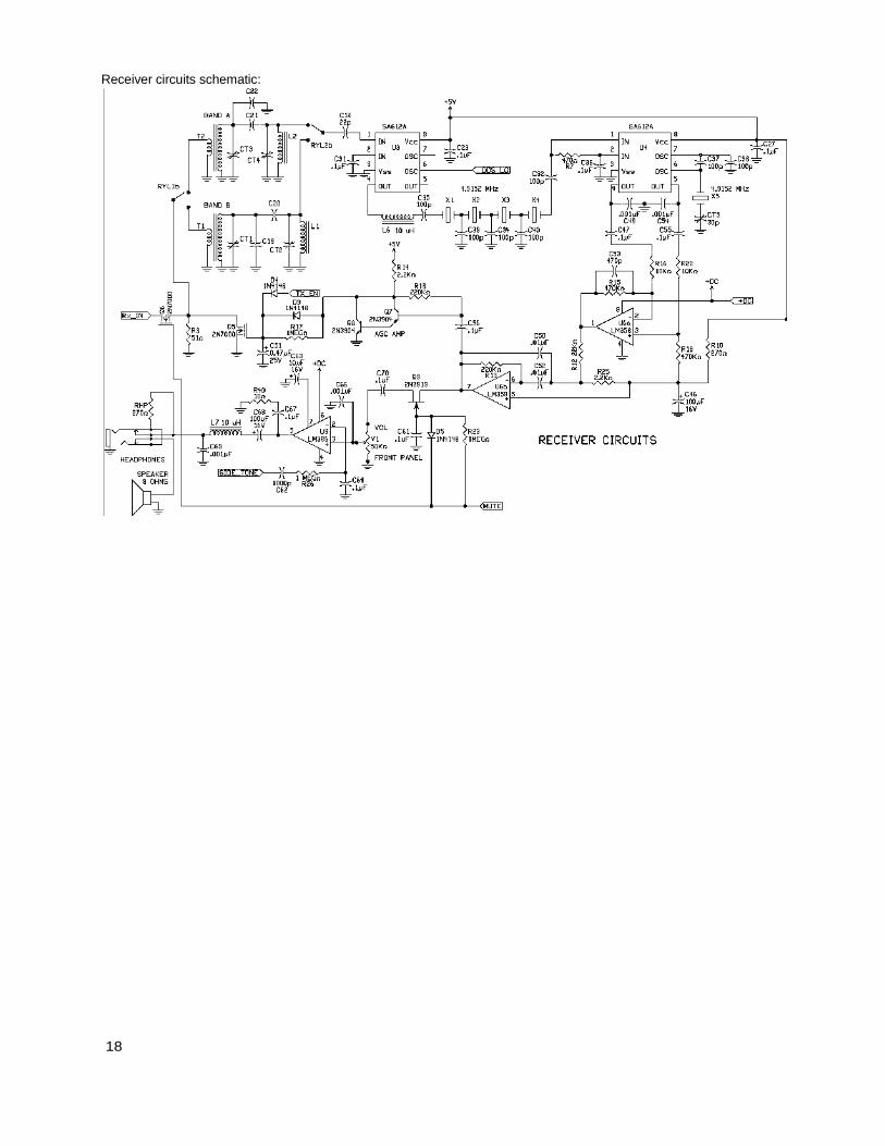
Receiver circuits schematic:
19
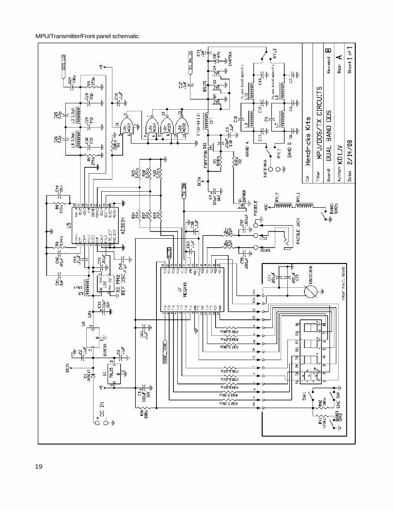
MPU/Transmitter/Front panel schematic:

20
How it works:
Signals from the antenna first pass through the transmitters Low Pass Filter, which are selected for the current operating band by two relays, RY1 and RY2. The receiver signal is picked off from the drains of the transmitters PA FETs and routed through a QSK switch, Q6 a 2N7000 MOSFET. During receive, this FET is biased ON to allow signal to pass through and a 51 ohm resistor, R3 is used to terminate the LPF to keep its frequency response correct.
The output of the QSK switch Q6 is then routed to the double tuned receiver input filter, which are selected by the other set of contacts on relays RY1 and RY2. The top of the second tuned circuit is connected to the input of the 1st mixer, U3, a SA612A Gilbert Cell active mixer. A Local Oscillator signal generated by the DDS (Direct Digital Synthesizer) is mixed in U3 to produce an IF frequency of 4.915 MHz. The output of the 1st mixer is then filtered by a four crystal IF filter to provide selectivity and opposite sideband suppression. The crystal filter is terminated by a 470 ohm resistor across the inputs of the product detector mixer, another SA612A (U4). This termination resistor helps flatten out the response of the filter. Without this termination, there would be peaks in the filter response.
The product detector mixer uses the on chip crystal oscillator function to generate the BFO signal needed to produce the audio beat note from the IF signal. The balanced output of the product detector mixer feed a balanced input audio amplifier. 0.001 ufd caps from the mixer outputs to ground by-pass RF products on the mixer output to ground. The output of the first audio amplifier (U6a, a LM358 dual op amp) then feeds an audio band pass filter. This filter has a peak response at 600 Hz and is used to help reduce high frequency hiss and provide some additional selectivity.
The output of the audio band pass filter is then routed through an audio mute switch, Q9. R23 and C61 on the gate of the FET switch delays the turn on time when going from transmit back to receive. This eliminates an audio “thump” caused by the RF QSK switching FET Q6 turning back on and propagates through the receiver circuits.
The output of the audio mute switch then goes to the volume control and then into the final audio power amplifier, U9 a LM386. A RF choke between the output of the audio amp and the speaker or headphones keeps which might be picked up by the speaker or headphone leads out of the amplifier, which can cause distorted or raspy side tone. Side tone, which is generated by the microprocessor, is feed into on the of the amplifier inputs though a low pass filter comprised of R26 and C64. This RC filter reduces the amplitude of the uP generated square wave signal and improves its sound. Injecting the side tone signal into the audio amplifier in this way allows for volume control independent side tone level.
AGC operation:
The audio signal from the audio band pass filter is amplified by a high gain Darlington pair amplifier, Q7/Q8. These transistors are normally biased into saturation by the base resistor R1 8. Negative going portions of the audio signal cause Q7/Q8 to start to turn off, allowing the collector voltage to rise. Diode D3 allows this voltage to charge C51, which holds the AGC voltage during positive portions of the audio signal and in conjunction with R17 provides the AGC “hang” time. The voltage on C51 is applied to the gate of Q5. When the voltage on the gate gets to be about 3 volts, Q5 starts to turn on. Since Q5 is connected across the signal input to the receiver, this attenuates the input signal.
AGC action does not start until an input signal reaches about S7 or 8 and stops being effective with signals above S9+20 dB. Although the AGC range is somewhat limited, it is enough to keep strong signals from becoming too loud and making you ride the volume control while tuning across the band. The AGC is also effectively disabled for weak signals, where AGC action can be more of a hindrance then a help. Because it takes several audio cycles for the AGC to respond, very strong signals can cause a slight “popping” sound as the leading edge of the signal will be at full volume. This is most noticeable if the code speed being sent is slower than the hang time of the AGC. The hang time is made relatively short so that it recovers quickly when coming out of transmit.
Transmitter:
The transmitter is very simple and effective. During transmit, the DDS chip produces the direct transmit frequency so no mixing and filtering is needed. It also generates a square wave signal, which is feed into some NOR gate high speed logic buffers. The DDS output is first inverted with U2a to produce a normally HIGH signal, then inverted again the remaining three gates in the chip which are connected in parallel to produce a normally LOW signal to apply to the PA FET gates.
Three BS170 MOSFETs connected in parallel are used for the power amplifier. The 5 volt square wave logic drive to the gates allows the MOSFETs to have a low “ON” resistance and switch on and off quickly. This produces a very efficient Class C amplifier, of about 70%. This high efficiency is the key to using PA transistors in TO-92 packages which do not get very warm, even when putting out 5 watts of RF power. The output Low Pass Filter is designed to provide some impedance matching between the PA and antenna load, which also improves efficiency.
In order to eliminate key clicks, the supply voltage to the PA is keyed on and off and has a few millisecond rise and fall time.
21
Q10, a P channel power MOSFET switches the supply voltage to the PA. The gate pull up resistor R1 in conjunction with C10 slows down the turn on and off times to provide the proper voltage ramp. Q1 connected back to the uP is used to turn Q10 on and off for keying.
Microprocessor control:
An Atmel MEGA48 processor is used to control the rig. This processor provides all the logic functions needed to control the DDS chip, operate the LED display, input switches, provide the keyer functions, generate side tone and do the T/R switching control.
dual_band_manual_051009