qrp transceiver for cw in kit form - qsl.net manual ingles.pdfegv-40 cw qrp transceiver page 1...
TRANSCRIPT

EGV-40 CW QRP Transceiver Page 1
EGV-40QRP transceiver for CW in kit form
In memory of Miguel Montilla, EA3EGV (SK)
Assembly manualLast update: Octubre 1st, 2013
[email protected] last minute updates and news, please got to: www.qsl.net/ea3gcy
Thanks for buying and building the kit for the EGV-40 transceiver
Enjoy building and working QRP! 73, Javier Solans, ea3gcy

EGV-40 CW QRP Transceiver Page 2
INDEX
INDEX……………………………………………………………………………………….………. 2
INTRODUCTION…………………………………………………………………………………… 3
SPECIFICATIONS………………………………………………………………………………….. 4
TIPS FOR FIRST TIME BUILDERS………………………………………...……………………. 5
PARTS LIST SORTED BY VALUE/QUANTITY………..…………………………..…………… 7
INDIVIDUAL PARTS LIST………………………..……….……………………………………….. 9
LOCATION MAP…….…………………………………………………………………………….. 13
ASSEMBLY…….………..……………….…..……………………………………....................... 14
ADJUSTMENTS AND CHECKS…………..…………………………………………………...... 24
APPENDICES………….…...……………………………………………………………….……… 28
IF YOUR KIT DOES NOT WORK AFTER ASSEMBLY.………………..……………………... 31
WARRANTY CLAUSES………........…………………………………………………………...... 33
SCHEMATICS..……..……………………………………………………………………………… 34
WIRING……..………..……………………………………………………………………………… 35

EGV-40 CW QRP Transceiver Page 3
INTRODUCTION
This EGV-40 transceiver is probably the kit that I have produced with more care and illusion in my life.It is a great honor to name this kit "EGV", the callsign suffix of the late Miguel Montilla, EA3EGV (SK).With no doubt, this is the kind of kit he liked most.It was my privilege to establish and share with him the first years of the EA-QRP Club. He has alwaysbeen a referent in my life; when I remember those wonderful years his humbleness, work capacity andgenerosity are the virtues which shine his image.How lucky I was to be able to share the path with you, Miguel! Thanks!
Javier Solans, ea3gcy
Miguel Montilla, EA3EGV (SK)Miguel got his A class callsign in 1983. He hold previously the call EC3BAY. He was a good CWoperator, highly respected among their peers. Holder of many awards and winner of several contests,Miguel enjoyed both the competition and sharing his time with a novel operator, patiently providinginformation to make a QSO.He published articles on the journal from URE (Spanish Radio Amateur Union) Unión deRadioaficionados Españoles, on “CQ Radio Amateur” (Spanish edition) and on the G-QRP bulletins, etc.But, without doubt, what he liked most it was QRP kit building. He loved to build a kit over a weekendand enjoy some placid QSOs made with his new fresh transceiver. Of course, always with the minimumpower required!Miguel EA3EGV was the founder member #1 of the EA-QRP CLUB.On September 1994 a group of four hams, Miguel Montilla EA3EGV, Miguel Molina EA3FHC, VicençLlario EA3ADV and myself, Javier Solans EA3GCY, founded the EA-QRP.Every April the club celebrates a CW contest: “EA-QRP-CW In memoriam EA3EGV”.
EGV-40The EGV-40 is not a novel design.The EGV-40 kit is a low power, CW transceiver designed to be simple and compact, using the legendaryNE/SA602 mixer chips. The circuit is a “tutti frutti” mix of several well known designs from the last 20-25years, very similar among them. In the EGV-40 I have tried to gather the best ideas of all these littlejewels but keeping in mind the philosophy of making an easy to build, compact, reasonably cheap circuitwith good characteristics.The EGV is not a technical marvel but... will something so simple work well?Build it, and you will be able to answer this question.
A high stability VXO covers around 40 kHz in the lower part of the band with very low drift: less than 200Hz in the first 5 minutes of the start-up. A "fine" tuning has been added, so no mechanical or electricalband-spread of the main tuning is required.Also, a variable attenuator has been included in the RX path to avoid the overload with the typical strongsignals in the band.

EGV-40 CW QRP Transceiver Page 4
AcknowledgmentsI want to thank Viçens EA3ADV, Lluís EA3WX and Alfons EA3BFL for their support and help to makethis kit happen. To Dave K1SWL (smallwonderlabs.com) for granting me permission to use on the EGV-40 some details of the transmitter circuit of his legendary SW-40.To Jon EA2SN for translating this manual into English, and to the “EA-QRP-CLUB” for keeping alive thehomebrewing, even on difficult times.And, in special, to Montse, Miguel's widow, for allowing me to link this EGV-40 kit with the memory of hislate husband, and for generously providing me with information and support.
SPECIFICATIONS
GENERAL:Frequency coverage: By means of a Variable Crystal Oscillator (VXO), tuning the CW segment of the 40meter band (40 kHz).Frequency control: High stability VXO, with a couple of crystals on 11.981 MHz.Antenna impedance: 50 ohm.Power requirements: 12-14 V DC, about 25 mA in reception (without signal), 380 mA (2.5 W) ontransmission.Part count: 36 resistors, 65 capacitors, 1 trimmer resistor, 2 trimmer capacitors, 3 potentiometers(volume, fine tune and attenuator), 7 IC's, 12 transistors, 6 diodes, 11 inductors, 5 IF transformers, 1variable capacitor (tuning), and 5 crystals.Front panel controls: Main tuning, fine tuning, volume.Back panel controls: RX attenuator.External connections: Headphones, key, antenna, DC connector.Board dimensions: 100x85 mm (around 4 x 3 1/2 in).
TRANSMITTER:RF output: from 0 to 3.5 W (at 13.8 V) internally adjustable (2.5 W recommended).2nd. harmonic output: -40dBc below the fundamental (at 2.5 W).Other spurs: all other spurs are -50dBc o lower with respect to the fundamental.T/R switching: Semi or full break-in (internally defined by changing a capacitor).Adjustable RX/TX shift.Sidetone monitor: through the receiver, picking an attenuated signal of the transmitter.Sidetone level: internally defined by changing a resistor.
RECEIVER:Type: Superheterodyne, one conversion Balanced mixer.Coverage: 7.0 to 7.04 MHz approx. (CW segment)Sensitivity: 0.25 µV MDS (minimum discernible signal).Selectivity: ladder filter with 3 crystals. Bandpass: 800 Hz nominal (at -6 dB)IF frequency: 4.915 MHz.Dual AGC system, controlling both the RX mixer and the product detector.Audio output: on headphones 150 mW (on 30-100 ohm loads).

EGV-40 CW QRP Transceiver Page 5
PLEASE, READ AT LEAST ONCE ANDTHOROUGHLY ALL THE ASSEMBLY INSTRUCTIONSPRIOR TO BUILDING SESSIONS.
TIPS FOR FIRST TIME BUILDERS
Tools Required:- Small tipped soldering of about 25-30 W rating, good quality soldering tin for electronic work, small sidecutters, wire strippers, long strippers, long nosed pliers, a sharp knife hobby "cutter”, a screw driver forthe M3 bolt, trimming tool for the IF cans.- You need a good light and a magnifying glass to see fine print on the parts and other building details.Instruments required:- Multimeter, Oscilloscope (desirable but not essential). Frequency counter or HF receiver. RF powermeter. 50 ohm, 5W load. RF Generator (desirable not essential).
Soldering:There are two important things which need to be done to ensure the successful operation of a kit. One isgetting the right part into the proper place on the board, the second is good soldering.
To solder properly, you must use the correct type of iron and the right quality of solder. Use a smalltipped soldering iron which has a bit that is short and almost pointed at end. The iron should be about25-30 Watts (if it is not thermostatically controlled). Use only electronic type multicored solder. NEVERuse any extra flux. You should hold the hot iron in contact with both the board and component lead forabout two seconds to heat them up. Then, keeping the iron in place, touch the solder onto the junction oflead and track and wait about two second or so until the solder to flow along the lead and track to form agood joint. Now remove the iron. The iron should have been in contact with the work piece for a totaltime of about 4 seconds in all. When soldering leads going to the ground plane of the board, you willneed to preheat the union longer to get a good flow of the molten tin.It is highly recommended to clean and remove the remaining tin from the iron tip after each soldering(most of the holders have a sponge for this); this helps to avoid old tin on the tip and residues fromprevious operations.

EGV-40 CW QRP Transceiver Page 6
Finding the right part:
IC’sThe outline on the board for the IC's has a “U” notch on one end, indicating pin 1 end of the IC. There isalso a notch on one end of the sockets. This end goes over the “U” notch outline on the board. Finally,pin 1 of the IC is marked with a round dimple or dot; this end of IC will go towards the notch on thesocket or “U” on the outline.
DiodesBe sure to observe proper polarity of diodes. There is a black band towards one end of the diode. Thisband should face the line shown on the diode outline of the board.
Electrolytic capacitors:These must be installed with the correct polarity. The positive (+) lead is always the long lead. Thenegative (-) lead is marked by a stripe on the body of the capacitor can. Make sure the plus end of thecap goes toward the hole labeled with the (+).
Coils and Transformers:You can find it convenient to wind and prepare all the coils and transformers before you start insertingparts. That way you don’t need to stop and possibly loose concentration to wind them.Is the part of the build considered by some to be the most difficult. I find it one of the easiest stages,personally, and almost relaxing. Just take your time. The assembly instructions and pictures illustrate theprocess.
EGV-40 CW QRP Transceiver Page 7
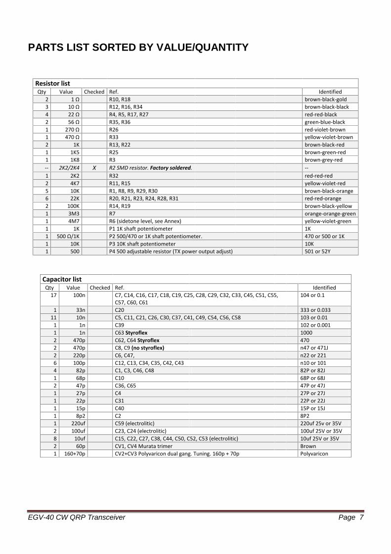
PARTS LIST SORTED BY VALUE/QUANTITY
Resistor listQty Value Checked Ref. Identified
2 1 Ω R10, R18 brown-black-gold3 10 Ω R12, R16, R34 brown-black-black4 22 Ω R4, R5, R17, R27 red-red-black2 56 Ω R35, R36 green-blue-black1 270 Ω R26 red-violet-brown1 470 Ω R33 yellow-violet-brown2 1K R13, R22 brown-black-red1 1K5 R25 brown-green-red1 1K8 R3 brown-grey-red-- 2K2/2K4 X R2 SMD resistor. Factory soldered. --1 2K2 R32 red-red-red2 4K7 R11, R15 yellow-violet-red5 10K R1, R8, R9, R29, R30 brown-black-orange6 22K R20, R21, R23, R24, R28, R31 red-red-orange2 100K R14, R19 brown-black-yellow1 3M3 R7 orange-orange-green1 4M7 R6 (sidetone level, see Annex) yellow-violet-green1 1K P1 1K shaft potentiometer 1K1 500 Ω/1K P2 500/470 or 1K shaft potentiometer. 470 or 500 or 1K1 10K P3 10K shaft potentiometer 10K1 500 P4 500 adjustable resistor (TX power output adjust) 501 or 52Y
Capacitor listQty Value Checked Ref. Identified
17 100n C7, C14, C16, C17, C18, C19, C25, C28, C29, C32, C33, C45, C51, C55, 104 or 0.1C57, C60, C61
1 33n C20 333 or 0.03311 10n C5, C11, C21, C26, C30, C37, C41, C49, C54, C56, C58 103 or 0.01
1 1n C39 102 or 0.0011 1n C63 Styroflex 10002 470p C62, C64 Styroflex 4702 470p C8, C9 (no styroflex) n47 or 471J2 220p C6, C47, n22 or 2216 100p C12, C13, C34, C35, C42, C43 n10 or 1014 82p C1, C3, C46, C48 82P or 82J1 68p C10 68P or 68J2 47p C36, C65 47P or 47J1 27p C4 27P or 27J1 22p C31 22P or 22J1 15p C40 15P or 15J1 8p2 C2 8P21 220uf C59 (electrolitic) 220uf 25v or 35V2 100uf C23, C24 (electrolitic) 100uf 25V or 35V8 10uf C15, C22, C27, C38, C44, C50, C52, C53 (electrolitic) 10uf 25V or 35V2 60p CV1, CV4 Murata trimer Brown1 160+70p CV2+CV3 Polyvaricon dual gang. Tuning. 160p + 70p Polyvaricon

EGV-40 CW QRP Transceiver Page 8
Semiconductors listQty Type Checked Ref. IdentifiedTransistors
8 BC547 Q1, Q2, Q5, Q6, Q7, Q8, Q10, Q11 BC5471 BC557 or BC558 Q9 BC557 or BC5582 J310 SMD X Q3, Q4 SMD Factory soldered --1 2SC2078/1969 Q12, washer and mica spacer C2078 or C1969
Integrated circuits3 SA/NE602 IC1, IC2, IC6 SA602AN or NE602AN1 LM386 IC3 LM386N-12 78L06 IC4, IC7 78L061 78L08 IC5 78L08
Diodes4 1N4148 D1, D2, D4, D5 41481 47V Zener D3 Zener 47V 1W BZX85C471 BB112 DV1 Varicap diode BB112
Inductors/RF Transformers/CrystalsQty Value Checked Ref. Identified
4 100uH L1, L3, L6, L8, Axial inductor brown, black, brown1 18uH L2 Axial inductor brown-grey-black1 22uH L4 Axial inductor red-red-black1 47uH L7 Axial inductor yellow-violet-black2 T37-2 L10, L11 LPF toroids 16t. 9,5 mm diam. red1 T68-2 L5 Toroid. Tuning inductor (47) 48t. 17,5 mm diam. red2 FT37-43 T5 toroid = 8 + 1 turns ; L9 toroid = 6turns 9,5 mm diam. black4 3334 (5u3H) T1, T2, T3, T4 5u3H Shielded coils K3334 or “5u3H”5 4.915 X1, X2, X3, X4, X7 Crystals 4.915MHz. 4.9152 11.981 X5, X6, 11.981MHz crystals 11.98
HardwareQty Value Checked Ref. Identified
5 nuts hex nuts M3 -4 spacers 5mm spacer for M3 screw -4 screw 5mm M3 screw -1 screw 10mm M3 screw -1 washer M3 lock washer -
13 pins Phone(2), KEY(2), VDC(2), ANT(2), VXO(2), J1A/B(3) -1 jumper jumper for J1 -4 IC socket IC’s socket 8 pin -1 Shaft Poly. 6mm Shaft Polyvaricon Hardware -1 Heatsink Q7 (Output Amp) Heatsink -
70cm wire 70cm enameled copper wire 0,5mm -110cm wire 110cm enameled copper wire 0,3mm -
1 EGV PCB 100mm x 85mm ILER V2 PCB -

EGV-40 CW QRP Transceiver Page 9
INDIVIDUAL PARTS LIST
ResistorsChecked Ref. Value Ident./Comment Circuit section Located
R1 10K brown-black-orange Rx mute C-8X X R2 2K2/2K4 SMD factory soldered AGC F-9
R3 1K8 brown-grey-red Q2 C-7R4 22 Ω red-red-black IC1 E-10R5 22 Ω red-red-black IC2 E-10R6 4M7 yellow-violet-green Q3 Mute (see text) H-8R7 3M3 orange-orange-green Q4 Mute H-9R8 10K brown-black-orange Q5 Mute G-9R9 10K brown-black-orange Q5 Mute G-10R10 1 Ω brown-black-gold IC3 Audio out G-5R11 4K7 yellow-violet-red IC3 Audio out F-6R12 10 Ω brown-black-black IC3 Audio out F-6/7R13 1K brown-black-red Q6 AGC G-7/8R14 100K brown-black-yellow Q6 AGC H-7R15 4K7 yellow-violet-red Q6 AGC H-7R16 10 Ω brown-black-black earphones out H-9/10R17 22 Ω red-red-black IC3 Audio out H-5R18 1 Ω brown-black-gold Fine G-3R19 100K brown-black-yellow Fine H-1/2R20 22K red-red-orange VXO Q7 E-3R21 22K red-red-orange VXO Q7 G-4R22 1K brown-black-red VXO Q7 F-4R23 22K red-red-orange VXO Q8 E-3R24 22K red-red-orange VXO Q8 F-4R25 1K5 brown-green-red VXO out E-4R26 270 Ω red-violet-brown VXO out E-4/5R27 22 Ω red-red-black Q10 C-4R28 22K red-red-orange Q10 C-3R29 10K brown-black-orange Q10 C-2R30 10K brown-black-orange Key in Q9 E-6R31 22K red-red-orange Key in Q9 E-6R32 2K2 red-red-red Q11 B-4/5R33 470 Ω yellow-violet-brown Q11 B-4/5R34 10 Ω brown-black-black Q11 B/C-4/5R35 56 Ω green-blue-black Q11 B-5R36 56 Ω green-blue-black Q12 A-2
PotentiometersChecked Ref. Value Ident./Comment Circuit section Located
P1 1K shfat potentiometer 1K RX atten. A-9P2 500 Ω/1K shaft potentiometer 500 or 470 or 1K Audio volume I-9P3 10K shaft potentiometer 10K Fine Tune I-2P4 500 Ω adjustable resistor 501 Power level B-3

EGV-40 CW QRP Transceiver Page 10
CapacitorsChecked Ref. Value Ident./Comment Circuit section Located
C1 82p 82, 82p or 82J RX BPF C-10C2 8p2 8p2 or 8.2 RX BPF C-9C3 82p 82, 82p or 82J RXBPF C-10C4 27p 27, 27p or27J RX BPF C-9C5 10n 103 or 0.01 RX MIX C-8C6 220p 220p, 220 or n22 RX MIX E-8C7 100n 104 or 0.1 RX MIX E-9C8 470p 471 or n47 IF Filter D-7C9 470p 471 or n47 IF Filter E-7C10 68p 68, 68p or 68J CW DETEC. F-7/8C11 10n 103 or 0.01 CW DETEC. F-8C12 100p 100, 100p or n10 CW DETEC. F-10C13 100p 100, 100p or n10 CW DETEC. F-9/10C14 100n 104 or 0.1 IC4 C-7C15 10uF 10uF IC4 C-6C16 100n 104 or 0.1 CW DETEC. E-9C17 100n 104 or 0.1 MUTE G-8/9C18 100n 104 or 0.1 MUTE I-7/8C19 100n 104 or 0.1 MUTE I-7/8C20 33n 333 or 0.033 MUTE I-7C21 10n 103 or 0.01 AGC F-7/8C22 10uF 10uF AGC H-7/8C23 100uF 100uF Audio AMP G-7C24 100uF 100uF Audio AMP H-6C25 100n 104 or 0.1 Audio AMP F-7C26 10n 103 or 0.01 Audio AMP F-5/6C27 10uF 10uF Audio AMP G-5C28 100n 104 or 0.1 Audio AMP H-5C29 100n 104 or 0.1 Audio AMP H-4/5C30 10n 103, 0.01 VXO G-3C31 22p 22, 22p or 22J VXO G-2C32 100n 104 or 0.1 VXO H-1C33 100n 104or 0.1 VXO H-2C34 100p 100p, 100 or n10 VXO G-4C35 100p 100p, 100 or n10 VXO F/G-4C36 47p 47, 47p or 47J VXO F-4C37 10n 103 or 0.01 IC5 G-4C38 10uF 10uF IC5 H-4C39 1n 102 or 0.001 TX MIX E-5C40 15p 15, 15p or 15J TX MIX E-4C41 10n 103 or 0.01 TX MIX C-4C42 100p 100, 100p or n10 TX MIX D-3C43 100p 100, 100p or n10 TX MIX E-3C44 10uF 10uF IC7 D-4C45 100n 104 or 0.1 IC7 D-3/4C46 82p 82, 82p or 82J TX MIX D-2C47 220p 220, 220p or n22 TX MIX C-1C48 82p 82, 82p or 82J TX MIX B-1C49 10n 103 or 0.01 DRIVER B-2C50 10uF 10uF DRIVER E-5C51 100n 104 or 0.1 DRIVER E-5C52 10uF 10uF Q9 Key in F-7C53 10uF 10uF DRIVER C-3C54 10n 103 or 0.01 DRIVER C-3C55 100n 104 or 0.1 DRIVER C-5C56 10n 103 or 0.01 DRIVER B-4C57 100n 104 or 0.1 DRIVER C-5C58 10n 103 or 0.01 Output AMP A-3C59 220uF 220uF Supply D-5

EGV-40 CW QRP Transceiver Page 11
Capacitors (continued)C60 100n 104 or 0.1 Output Amp C-5/6C61 100n 104 or 0.1 Output Amp A/B-6C62 470p 470 (Styroflex) LPF A/B-6C63 1000p (1n) 1000 (Styroflex) LPF A-6/7C64 470p 470 (Styroflex) LPF A-7/8C65 47p 47, 47p or 47J RX switch C-7CV1 60p Trimmer (brown) CW Detector G-10CV2+CV3 160+70p Var Tuning Polyvaricon VXO I-5/6CV4 60p Trimmer (brown) TX Mix E-1
CrystalsChecked Ref. Frequency Ident./Comment Circuit section Located
X1 4.915Mhz 4.915 IF D-7/8X2 4.915Mhz 4.915 IF E-7/8X3 4.915Mhz 4.915 IF E-7/8X4 4.915Mhz 4.915 RX DETEC. F-10X5 11.981Mhz 11.98 VXO F-3X6 11.981Mhz 11.98 VXO F-3X7 4.915Mhz 4.915 TX MIX E-2
SemiconductorsCheked Ref. Type Ident./Comment Circuit section Located
TransistorsQ1 BC547 BC547 MUTE B/C-9Q2 BC547 BC547 IF D-8
X X Q3 J310 SMD factory soldered MUTE H-8X X Q4 J310 SMDfactory soldered MUTE H-9
Q5 BC547 BC547 MUTE G-9Q6 BC547 BC547 AGC G-7/8Q7 BC547 BC547 VXO F/G-4Q8 BC547 BC547 VXO E-4Q9 BC557or BC558 BC557 or BC558 KEY switch E-6Q10 BC547 BC547 DRIVER C-2/3Q11 BC547 BC547 DRIVER C-4Q12 2SC2078 or 1969 C20178 or C1969 Output Amp A-5
IC'sIC1 NE602/SA602 NE602/SA602 RX MIX D-8/9IC2 NE602/SA602 NE602/SA602 CW DETEC F-9IC3 LM386N LM386N Audio AMP G-6IC4 78L06 78L06 RX C/D-6IC5 78L08 78L08 VXO H-3IC6 NE602/SA602 NE602/SA602 TX MIX D-3IC7 78L06 78L06 TX MIX D-4
DiodesD1 1N4148 1N4148 AGC H-7D2 1N4148 1N4148 Output AMP A-2D3 Zener 47V 1W BZX85C47 Output AMP C-5D4 1N4148 1N4148 RX limiter B-8D5 1N4148 1N4148 RX limiter B-9DV1 BB112 Varicap diode BB112 VXO (Fine) G/H-1

EGV-40 CW QRP Transceiver Page 12
Inductors/RF TransformersChecked Ref. Value/Type Ident./Comment Circuit section Located
L1 100uH Axial inductor brown-black-brown CW DETEC C-8/9L2 18uH Axial inductor brown-grey-black IF F-7L3 100uH Axial inductor brown-black-brown CW DETEC F-8L4 22H Axial inductor red-red-black CW DETEC G-10L5 T68-2 red toroid 48 turns (see text) VXO F-1/2L6 100uH Axial inductor brown-black-brown VXO G/H-3L7 47uH Axial inductor yellow-violet-black TX MIX E-1L8 100uH Axial inductor brown-black-brown DRIVER D-5L9 FT37-43 black toroid 6 turns (see text) Output AMP B-6L10 T37-2 red toroid 16 turns (see text) LPF B-7L11 T37-2 red toroid 16 turns (see text) LPF B-8
T1 5u3H (shielded) RF transf. 5u3H RX BPF B-10T2 5u3H (shielded) RF transf. 5u3H RX BPF D-10T3 5u3H (shielded) RF transf. 5u3H TX MIX D-1T4 5u3H (shielded) RF transf. 5u3H TX MIX B-1T5 FT37-43 black toroid 8 + 1 turns (see text) Output AMP A-4

EGV-40 CW QRP Transceiver Page 13
LOCATION MAP

EGV-40 CW QRP Transceiver Page 14
ASSEMBLY
You may use “individual parts list” or the “value/quantity parts list”. The “value/quantity parts list” is thequickest way to place components because all parts of the same value or type can be placed one aftereach other. You will need, however, the “individual parts list” to know how each part is identified and itslocation on the board. According to your personal experience you may prefer to use the individual list, toplay on the safe side. The location of all parts is very easy when using the 90 quadrants map. Afterplacing each component, you can mark it in the “checked column list”.It is highly recommended to inventory all parts to make sure everything is available and ready forassembly. Each builder may have his/her own way of organizing parts, but if you do not, you might tryusing a block of Styrofoam packing material and poke the parts on it. Parts may be sorted by type, value,and size (ohms, micro-farads etc).
RECOMENDED ASSEMBLY SEQUENCE ResistorsThe resistors are installed first. Place all resistors from R1 to R36 and the P4 trimmer (transmitter outputpower adjustment).DO NOT install now the potentiometers P1 (RF attenuator), P2 (volume) and P3 (fine tuning).Refer to the parts list, select the first resistor, R1 and locate its place on the board. This resistor is placedvertically; you need to bend only one leg. Most of the resistors are placed horizontally; bend their leadsas close to the ends as possible, and fit them into the holes marked on the silkscreen of the PCB. Takecare and avoid mixing resistors and axial inductors, which are a bit thicker. All resistors have a lightyellow body color with a gold band at one end. The resistor's leads once inserted, push the body down tolay flat on the PCB, and on the other side bend slightly out the legs to hold the resistor in place. Thenturn the PCB over and solder the leads to the PCB pads. Make sure the resistor body lays flat over theboard to keep its legs as short as possible.

EGV-40 CW QRP Transceiver Page 15
Please read the notes on soldering Poor soldering is the most common cause of a kit failing to work firsttime, so please take the soldering advice at heart! Once soldered cut off the excess length of the partlead as close to the joint as possible. Install all resistors from the parts list and carry on until all resistorsare soldered in place.Values which are in decade increments may be easily confused, such as 470, 4K7 and 47K. So, take agood look at the colors before you solder the part in place! In case of doubt, use a multimeter to checkthe resistor value.R2 is an SMD resistor, factory installed.
Axial inductorsL1, L2, L3, L4, L6, L7, L8.These components look just like fat resistors, but they have a blue or green colored bodies. Inside thedevice is a small coil wound on ferrite material. As before, refer to the parts list to select the correct onefor each position. L1, L2, L3, L4, L6 and L7 are mounted vertically. L8 is the only inductor horizontallyplaced, and we recommend to separate it from the board approximately 1-1.5 mm (1/16 in).Fit them on their designated places as with resistors.Note: L5 is the VXO toroidal coil, which will be wound and placed later.

EGV-40 CW QRP Transceiver Page 16
DiodesNow install the diodes, taking care to place them with the right orientation. There is one band at one endof each diode’s body which has to match the silkscreen of the PCB.D1, D2, D4 and D5 are 1N4148 types, these are usually orange with a black band, marked with “4148”on their body. D4 and D5 are placed vertically, all others are placed horizontally.D3 is similar to the 1N4148 ones but thicker, and it is marked as BZX85C47.DV1 is a BB112 varicap diode and is similar to a transistor with only two legs; its outline should fit thesilkscreen of the PCB.
CapacitorsThere are Ceramic, Polyester, Styroflex and Electrolytic type capacitors. All these have their valueprinted on the body. Go to the parts list' “identified” column.When fitting them, keep their leads as short as possible.C62, C63 y C64 are Styroflex capacitors, they are axial and must be placed vertically.Values which are in decade increments may be easily confused, such as 8p2, 82p and 820 p. So, take agood look at the printed numbers before you solder the part in place!Electrolytic capacitors must be fitted the right way around: the LONGER LEAD goes to the hole marked“+”, the shorter lead is "-" and it is indicated by a band along the body of the capacitor with “-“.CV1 and CV4 are capacitor trimmers brown in color. They have no printed marks. Place them followingthe outline on the silkscreen of the PCB.CV2 + CV3 are part of the two-section tuning “Polyvaricon” variable capacitor. DO NOT INSTALL it now.

EGV-40 CW QRP Transceiver Page 17
Pin “headers”Place and solder pins for “Phone”(2)(H-10), “KEY”(2)(D-6), “VDC”(2)(D-6), “ANT”(2)(A-7), “VXO”(2)(F-5),and J1 A/B(3)(I-4).Turn the board over and hold the headers in place with the help of a female jumper while you solderthem avoiding burning your fingers. Use the other hand for the soldering iron and move the boardtowards the tin to solder the headers in place. If you have someone to help out, much better!
TransistorsAll of them have their type numbers marked on their body. Place and solder Q1, Q2, Q5, Q6, Q7, Q8,Q9, Q10 and Q11 following the outline on the silkscreen.Q3 and Q4 are SMD J310 transistors, and they are factory soldered on the tracks side of the PCB.DO NOT INSTALL Q12 now (TX power amplifier).
Integrated CircuitsThe outline on the board for the ICs has a “U” notch on one end, indicating the pin 1 end of the IC. Thereis also a notch on one end of the sockets. This end goes over the “U” notch outline on the board. Finally,pin 1 of the IC is marked with a round dimple or dot; this end of IC will go towards the notch on thesocket or “U” on the outline.Install sockets for IC1, IC2, IC3, and IC6 on their PCB locations. Make sure that all sockets lie flatagainst the board. Next, insert IC1, IC2, IC3, and IC6 on their sockets.
IMPORTANT: Make sure that all IC’s are fully inserted on their sockets, push them if need be. It is agood idea to clean or scratch the legs of the chips prior to their insertion on their sockets. If contact failsin the sockets it may cause a malfunction of the rig.Now, place the voltage regulators IC4, IC5, and IC7, following the outline of the silkscreen.

EGV-40 CW QRP Transceiver Page 18
CrystalsInstall X1 to X7.X1, X2, and X3 are part of the CW filter, X4 is the RX BFO crystal, and X7 is the oscillator for the TXmixer. These crystals have been hand picked (have handwritten numbers on their body) to have thesame resonating frequency, in order to obtain the best filter quality. The X5 and X6 pair are the VXOcrystals.The crystal housing should not touch the board, place them slightly separated from the board. 0,5-1 mm(less than 1/16 in) may be sufficient.
Toko shielded coils (cans)T1, T2, T3 y T4 are Toko “5u3“ cans (Toko KANK3334). RF transformers for the bandpass filters Makesure their body lay flat against the PCB.You may need extra heat to solder the shield tabs.

EGV-40 CW QRP Transceiver Page 19
When you turn the board over the cans may fall. Fit the can in place, hold it with one hand, and turn theboard over. Use the other hand for the soldering iron, and move the board towards the tin to solder thecan in place. If you have someone to help out, much better!
Toroids L10 y L11 for the LPFL10 and L11 are identical. T37-2 cores (red toroids with OD 9.5 mm / 0,375 in) are used.Cut 25 cm (10”) of 0.5 mm enameled wire and wind 16 turns on the red toroidal T37-2 core. Wind thewire tightly on the core, avoiding loose turns, and spread the turns evenly around the core. They shouldbe uniformly spread around the circumference of the toroid. Leave pigtails of about 10 mm (0.4”).Remove the enamel with a cutter to solder the toroids on the board.The nominal value for L10 and L11 is 1.02 µH.Counting turns: every time the wire passes through the toroid center hole counts as one turn.Important: Wind the toroid exactly as shown in the pictures.
Toroidal transformer T5T5 is an impedance matching transformer. A FT37-43 is used (black toroid with an OD of 9.5 mm /0.375 in). It has a primary of 8 turns, going to “b” and “b1” holes in the PCB and one secondary of 1 turngoing to “a” and “a1” holes.

EGV-40 CW QRP Transceiver Page 20
- Cut 15 cm (6”) of 0.5 mm enameled wire and wind 8 turns on the black FT37-43 toroidal core. Windthe wire tightly on the core, avoiding loose turns, and spread the turns evenly around the core. Theyshould be uniformly spread around the circumference of the toroid. Leave pigtails of about 10-20 mm(0.70”).- Now take a resistor leftover of 15 – 20 mm (1/2-3/4 in) to make the 1 turn secondary (remember, oneturn means that the wire goes once through the toroid core). Please try to make a snug fit of this turn tothe core.- Prior to its soldering, use a cutter, or sandpaper to scrape the enamel from the pigtails of the 8 turnwinding.
IMPORTANT: Wind the T5 transformer exactly as shown in the pictures. You must follow both thenumber of turns and the winding direction.

EGV-40 CW QRP Transceiver Page 21
L9 ToroidL9 is an inductor acting as a collector choke on the TX power amplifier transistor. A FT37-32 is used(black toroid with an OD of 9.5 mm / 0.375 in). It has 6 turns.Cut 12 cm (5”) of 0.5 mm enameled wire and wind 6 turns on the black FT37-43 core. Wind the wiretightly on the core, avoiding loose turns, and spread the turns evenly around the core. They should beuniformly spread around the circumference of the toroid. Leave pigtails of about 10 mm (0.4”). Removethe enamel of the pigtails with a cutter prior to soldering the toroid on the board.The nominal value for L9 is 12.6 µH.
Tuning Polyvaricon capacitor for the VXO CV2/CV3Install the hardware shaft on the polyvaricon.Place the Polyvaricon over the board at a distance of 3-5 mm (see picture). This eases the fitting of thevariable cap to the front panel. Do not solder it until you know exactly how you are going to install theboard on the box.You may want to mount the polyvaricon out of the board. This may be a good idea, but place it asclose as possible and use short and rigid wires. Even small movements may affect the tuning!

EGV-40 CW QRP Transceiver Page 22
This polyvaricon contains two variable tuning capacitors inside. With the external jumpers J1 A/B youmay select which section you will use; with the jumper in "B" you will use CV2, the larger capacitor, whileon "A" the smaller CV3 will be used.
CV2 has about 150 pF, CV3 only 70 pf.In the back of the capacitor there are two padders (small trimmers) for a fine adjustment. The one in thelower part “X” (close to the terminals) goes in parallel with CV2, and the one on top “Z” is for CV3.Adjusting these you may change the upper limit of the band coverage by some 10-15 kHz! Youwill have to adjust the upper limit with the polyvaricon in its minimum capacity (turned all the wayclockwise). These adjustments will be carried out later on, in "ADJUSTMENTS AND CHECKS".
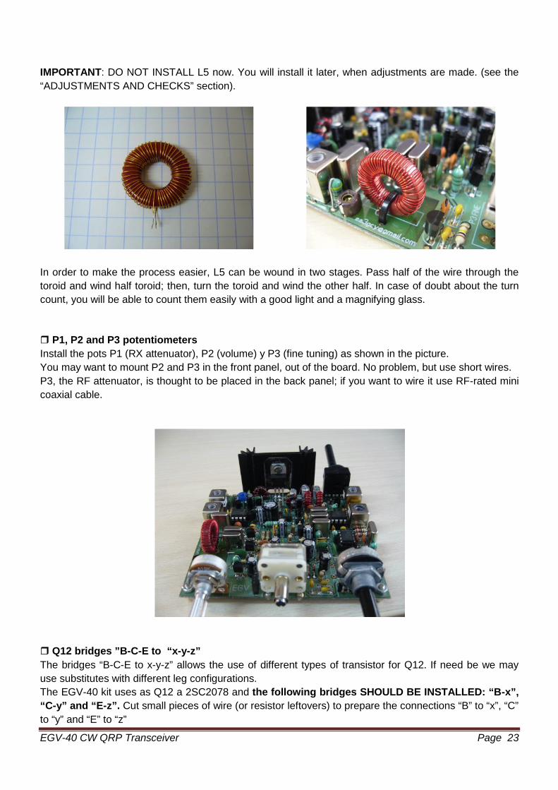
IMPORTANT:- If you want to wire the polyvaricon out of the board, please take notice that, when mounting it withterminals up the connections get inverted and J1 A/B should be changed from J1B to J1A and viceversa.- When screwing the polyvaricon to the front panel (M2,5 x 5 screws) take care not to drive the screwstoo much; they may block the internal mechanism of the polyvaricon. If needed, add one or morewashers avoid this kind of trouble L5 Tuning inductor of the VXOA T68-2 is used (red toroid with an OD of 18 mm / 0.690 in).Cut 102 cm (40 in) of 0.3 mm enameled wire and wind 48 turns on the T68-2. Leave pigtails of 10-15mm (3/8-1/2 in).
EGV-40 CW QRP Transceiver Page 23
IMPORTANT: DO NOT INSTALL L5 now. You will install it later, when adjustments are made. (see the“ADJUSTMENTS AND CHECKS” section).
In order to make the process easier, L5 can be wound in two stages. Pass half of the wire through thetoroid and wind half toroid; then, turn the toroid and wind the other half. In case of doubt about the turncount, you will be able to count them easily with a good light and a magnifying glass.
P1, P2 and P3 potentiometersInstall the pots P1 (RX attenuator), P2 (volume) y P3 (fine tuning) as shown in the picture.You may want to mount P2 and P3 in the front panel, out of the board. No problem, but use short wires.P3, the RF attenuator, is thought to be placed in the back panel; if you want to wire it use RF-rated minicoaxial cable.
Q12 bridges ”B-C-E to “x-y-z”The bridges “B-C-E to x-y-z” allows the use of different types of transistor for Q12. If need be we mayuse substitutes with different leg configurations.The EGV-40 kit uses as Q12 a 2SC2078 and the following bridges SHOULD BE INSTALLED: “B-x”,“C-y” and “E-z”. Cut small pieces of wire (or resistor leftovers) to prepare the connections “B” to “x”, “C”to “y” and “E” to “z”

EGV-40 CW QRP Transceiver Page 24
Take care and avoid any shortcircuits between bridges.
Q12 capsule (2SC2078) should be electrically isolated from the heatsink. Use the plastic washer and themica sheet provided with the kit. Once the transistor is fitted over the heatsink, check with a multimeterthat there is no continuity between the transistor tab, the screw and the heatsink. Use the insulatingmaterial and an M3 screw and nut. It is also recommended to apply a dab of thermal grease.You may also drill other hole on the heatsink if that suits better its position on your box.
DO NOT OPERATE the transceiver without a heatsink on Q12

EGV-40 CW QRP Transceiver Page 25
ADJUSTMENTS AND CHECKS
Preliminary testing- Adjust P2 (volume), P3 (fine tuning), and P4 (TX output power) to mid position.- Turn P1 (RF attenuator) all the way clockwise.- Connect headphones to the header “PHONE” on the board.- Connect a PSU (12-14 V) to the “VDC” header on the board.- Measure the voltage on the following points (related to the receiver path):8 V from any leg of L6 and ground.6 V from any leg of R4 or R5 and ground.- Turn the volume (P3) to the maximum; you will hear a hiss on the headphones.
If all is OK, you may continue.
If not, please check your kit (see section "If your kit does not work after assembly")
Tuning adjustment of the inductor L5 and the Polyvaricon CV2/CV3NOTE: it is recommended to make all VXO adjustments with the "fine tuning" pot in its mid position; thisway, once tuned the pot will allow you some extra coverage at both ends of the tuning range.
The following task is more fun that you may think at first; it is not a "plug&play” one, but it is fun; leaveone hour of relaxed time and enjoy it!Solder the L5 pigtails on their place over the board. Leave it for now some slack, so you may compressor spread the turns. Connect a frequency counter on the “VXO” header. If your counter has a low inputimpedance, insert between the counter and the header a resistor (470 ohm or more) or a smallcapacitance cap (try with 22 pF or less) to reduce the interaction between the counter and VXO.If you don't have access to a counter, you may use an SSB or CW receiver with a digital dial coveringthe VXO frequency around 11.950 MHz. Connect to the receiver antenna input a length of wire with asmall loop and place it over the EGV-40.Note: A counter is highly recommended as the use of the receive is cumbersome.On TX, the IF frequency of 4.915 MHz is subtracted from the VXO frequency to obtain the RF outputsignal. For instance: 11.945 – 4.915 to get 7.030 MHz.On RX, the antenna signal is subtracted from the VXO frequency to obtain the IF frequency. Forinstance: 11.945 – 7.030 to get the IF of 4.915 MHz.
In both cases VXO = RF + FI
The polyvaricon capacitor contains two variable caps for tuning. J1 selects which section to use. Placinga jumper on “B” the larger CV2 (around 150 pf) is selected. Placing a jumper on “A” the smaller CV3 (70pf) is selected.For normal use on the EGV-40 the jumper should be placed on J1 “A” (smaller capacity) you canalso try the place J1 “B”. When the polyvaricon is placed out of the board, please notice that whenmounted upside down, with the terminals up, the jumper connections get inverted, and you will have toplace the jumper on J1 "B" instead of J1 "A".

EGV-40 CW QRP Transceiver Page 26
Lower limit of frequency.You may change the tuning coverage by spreading or compressing the turns. When the turns arecompressed, the inductance increases and, thus, the coverage is larger (the lower limit decreases).When turns are spread, the inductance and, thus, the coverage diminishes. Spreading or compressingthe turns a variation of a few kHz may be achieved.The EGV-40 has been designed to have a lower limit of the tuning range around 7.000 MHz.
Higher limit of frequency.In the back of the polyvaricon there are two padders (adjusting trimmers) “X” and “Z” to be used for thefine tuning. The one below, “X”, goes in parallel with CV2 (J1-B) and the one on top, “Z”, is for CV3 (J1-A). These padders may move the upper limit up to about 10-20 kHz! Make this adjustment with thepolyvaricon on its minimum capacity (all the way clockwise). The EGV-40 has been designed to allowthe adjustment of the upper limit of the coverage to 7.040 MHz.
Please see some examples as an orientation:
CV3 L6= T68-2 48 turns. Minimum MaximumX5-X6 = 11.981Mhz. MHz MHz MHz MHz
VXO RF VXO RF RangeTurns widely spread 11.925 7.010 11.950 7.035 30 kHzTurns less spread 11.915 7.000 11.958 7.043 43 kHzTurns compressed 11.900 6.090 11.955 7.040 50 kHz
When the turns spread is changed, you may need to readjust slightly the “padder” on the polyvaricon tokeep the tuning upper limit near 7.040MHz.

EGV-40 CW QRP Transceiver Page 27
Once VXO coverage suits your needs you will have to secure L5 on its position on the board.The best and cleanest option is to use a plastic retaining clamp throughout the holes on the board, asshown in the picture.Once the clamp is fastened you will still have some slack to move a bit the turns and make slightadjustments. Once done, you may use nail polish to fix the turns.If you plan to use silicone or glues, please notice that, due to their composition, they may affect largelythe characteristics of L5, even after curing. They also may absorb humidity, affecting its stability.
L6 should remain well fixed, it is very important, since vibrations may change the VXO frequencycausing "tremors" on the received and transmitted signals.Prior to the L5 final fix to the board make all the adjustments and checks of the rig and confirm that thefrequency coverage suits your needs.
Do not worry too much about the exact margin; is it so important to end at 40, 41 or 42 kHz?If you are dexterous, you may draw a dial in the front panel, with a scale to help you as a guide. RX adjustment. T1 and T2 bandpass. BFO oscillator CV1
T1-T2 bandpassNote: for this adjustment you will need a trimming tool for this kind of IF cans; if you use a screwdriver you maybreak and damage the coil core.Turn P1 (RX attenuator) to minimum attenuation, that is, all the way clockwise.

EGV-40 CW QRP Transceiver Page 28
If you have access to a RF generator, inject through the antenna header a signal on the receiving rangeof about 1-2 µV, tune the receiver into it, and adjust alternately T1 and T2 until you get the maximumsignal on the headphones.If you don't have access to instrumentation, do not worry, as these adjustments are not critical at all.Connect an adequate antenna for 40 meters to EGV-40 and tune a strong CW signal, as stable aspossible; adjust alternately T1 and T2 until you get the best reception on the headphones.
BFO oscillator CV1Once you have the input bandpass filter (T1-T2) adjusted, you will have to adjust the CV1 trimmer toobtain the best CW note that suits your taste.Although this adjustment is not very critical, it is more important that it seems at first; the signalsshould sound bassy, and check also that this adjustment has an influence on the oppositesideband suppression.
If you have access to a good counter with a sensible, high impedance input, try measuring the frequencyon pin 6 or 7 of IC2 and adjusting CV1 to measure something between 4.9140 – 4.9141 MHz.
Note: some counters are not sensible enough or present a large load, changing the oscillating frequencyand providing fake readings. You may try inserting between the counter and the pin a resistor (470 ohmsor more) or a small cal (22 pF or less) to reduce the interaction between the counter and the BFO.
REMEMBER: All transmission checks should be done with a 50 ohm load connected tothe transmitter output.DO NOT OPERATE the transceiver without a heatsink on Q12.
Adjustment of the TX, T3 and T4 bandpass filter. Adjustment of CV4, TX shift.Note: for this adjustment you will need a trimming tool for this kind of IF cans; if you use a screwdriver you maybreak and damage the coil core.Connect a power meter and a 50 ohm load to the antenna connector. Turn P4 (power control) to midposition.Connect a Morse key to the "KEY" headers and use the key to activate the transmitter (or shortcircuit the"KEY" headers.) You will notice that the receiver mutes and a reading on the wattmeter. Adjustalternately T3 and T4 to peak the power. With P4 on its mid position you will get some 2-2.5 W outputpower.
Put the headphones on and, while on TX, listen the sidetone monitor; turn CV4 until you hear a tone thatsuit your tastes. This adjustment can be done by ear, it is not critical at all, but usually the TX/RX shiftlies around 600-700 Hz.Please notice that the EGV is receiving its own transmitted frequency: the tone you are hearing is thesame as the shift, the offset, of your transmission.If you have access to an audio frequency meter you may check the frequency by measuring it at theheadphone output.
Notes:- While you are doing the transmitter adjustments, it is a good idea to touch Q12 heatsink every coupleof minutes to check it is not overheating.- If you plan to use always the same output power it is recommended to replace P4 with two fixedresistors of a similar value that the ones measured on P4 at the desired power.

EGV-40 CW QRP Transceiver Page 29
APPENDICESAppendix 1. “PHONE” headphone output. R16 limiting resistor.The EGV-40 has not been designed to be used with loudspeakers directly.On the "PHONE" header you may connect only headphones. Please use adequate headphones; badones will degrade the final outcome of your receiver. When checking several headphones, results will bevery different and for us, hams, in many cases the most expensive headphones are not the best.Sometimes low cost headphones may result ideal for the purpose of listening to the EGV-40; this may bedue to their sensitivity and the audio response, which may fit better the bandwidth required for the CWsignals.If you plan to use the EGV-40 at home, you may get very good results with PC multimedia speakers withtheir own amplifier (use 2.0 types of good quality, as systems with “sub-woofer” or "home cinema" arenot adequate.)
-R16 limits the output level to the headphones and protects the audio amplifier in case of a shortcircuit atthe output.
Appendix 2. Transmitter power amplifier transistor Q12.The 2SC2078 transistor included with the kit has been selected for the EGV for being a good outputtransistor for HF.In case of need you may use others. Some transistors used on CB transceiver such as the 2SC2166 or2SC1969 may be also used and offer a similar result. In some cases the terminal distribution is different.The bridges “B, E, C” - “x, y, z” will allow you to use any kind of TO-220 transistor as Q12.Notes:- Some transistors may have higher gain and, depending on their manufacturer, may be prone to auto-oscillations.- Many of this kind of HF transistors offered in the market at low price are fakes and work bad or do notwork at all.
Appendix 3. The VXO as local oscillator.Why are we using a VXO?The classical -and economical- alternative to the VXO is a simple Variable Frequency Oscillator (VFO) ora Voltage Controlled Oscillator (VCO). In order to get very clean mixing products when an heterodynesystem is used, it is recommended for both RX and, especially, for TX to use a Local Oscillator (LO)located over the Intermediate Frequency (IF), in our case 4.915 MHz, and over the working frequency, inour case 7.000 MHz. It will be possible to build a VFO LO on 2.085 - 2.125 MHz quite cheap and stable,but the mixing products on RX and TX will not be as clean as the ones produced with an LO on 11.9MHz, as generated on the EGV-40 VXO.The other option, a PLL driven VCO, will be adequate but expensive and cumbersome taking intoaccount the number of parts required.If you want to have a very precise transceiver, with high stability and digital dial, an excellent alternativeis the use of a DDS circuit. I will recommend you the ILER-DDS from EA3GCY.Note:If you have bought the EGV-40 and the ILER-DDS you don't need to install any of the parts related to theVXO circuit. Please see Appendix 7.
Appendix 4. Sidetone level. R6 value.The sidetone level is fixed by R6. With the R6 resistor included with the kit the sidetone level is sufficientbut soft. You may change the value between 1 M and 10 M to get the required level.

EGV-40 CW QRP Transceiver Page 30
Appendix 5. Full-Break-in delay. C17 value.The TX/RX switching delay may be modified by exchanging C17 with a cap of different value. The kitincludes a C17 cap of 100nF, getting a delay of 300-400 ms. You may increase or reduce the value ofC17 to increase or reduce the delay. If you remove C17, you will be able to work with Full Break-in, but itis recommended to include a small capacitor to get a delay of some tens of ms to avoid switching clicksand noises.
Appendix 6. “Fine tune” coverageThe P3 control acts as a fine tuning associated to the main tuning carried out by the polyvaricon and,obviously, they both work on RX and TX.If you prefer to use a mechanical reduction on the shaft of the polyvaricon or a larger diameter button,you may disable the P3 pot but just removing it from the PCB; we recommend that, instead, you placetwo 4K7 resistors to keep the overall coverage of the VXO as previously adjusted. If you removecompletely the "Fine tuning" circuit, including the DV1 varicap diode, the upper frequency limit may lieabove the CW segment with no adjustment possible to lower it.The "Fine tuning" control changes 1-2 kHz in the lower part of the coverage range and 5-6 kHz in theupper part. This is due to the nature of the circuit, the lack of linearity on the tuning circuit, and the factthat a similar change on the capacity external to the polyvaricon affects differently to the tuned frequencydepending on the part of the band.
Use of the “Fine tuning” controlWe recommend to place it normally on its mid position. Once you have find a station with the Main tuningcontrol, move the Fine tuning to tune it spot on. Once you have finished the QSO, or when you want tosearch for other stations, return first the Fine tuning control to its mid position.Note: You may change the coverage of the “Fine tuning” control by changing the value of the capacitorC31 and/or the resistor R18.
Appendix 7. Use of the ILER-DDS with the EGV-40The ILER-DDS offers a high stability oscillator against temperature changes, with a 10 Hz resolution andfrequency reading on an LCD. Moreover, the ILER-DDS may be configured to work with any other IFvalue, place band limits, quickly change the tuning steps, display the PSU voltage, etc.-If you have a working EGV-40 with its VXO and want to install an ILER-DDS, you need to disable theVXO by just disconnecting L6 and connecting the DDS output to the "VXO" header on the EGV-40.-If you have bought the EGV-40 and the ILER-DDS and you want to install it from scratch you don't needto install any of the parts related to the VXO circuit with the exception of R26.The following list gathers the parts related to the VXO that you don't need to install if you plan to usealways the rig with the ILER-DDS:
R18, P3, R19, R20, R21, R22, R23, R24, R25, and pot P3C30, C31, C32, C33, C34, C35, C36, C37, C38, and Polyvaricon CV2/CV3L6, L5, DV1, Q7, Q8, IC5, X5, and X6
Appendix 8. IF bandwithThe nominal bandwidth of the IF filter is of 800 Hz (at -6 dB). This offers a good selectivity for an easylistening of the CW signals. The IF bandwidth, however, may be modified by simply exchanging the capson C8 and C9. You may reduce their value down to 100 pf to get a wider bandwidth (less selectivity).This change produces some mismatches on the terminating impedance and the ripple on the filterresponse may increase, but most of the time you will not notice it.

EGV-40 CW QRP Transceiver Page 31
IF YOUR KIT DOES NOT WORK AFTER ASSEMBLYDon't worry, it is not uncommon a non working kit on the first try; be calm as in the majority of cases theyare small mistakes with a simple fix.Most faults are due to poorly soldered connections or misplaced parts; it is very rare to find a faulty part.Before taking any measurements with instruments, check all connections, inspect your soldering worklooking for cold connections, shortcircuits between tracks, sockets not making good contact, or partsplaced in the wrong place.If your kit does not work after final assembly, please follow these steps in order:
-Double-check every step in the assembly manual, pads soldered, and right parts placed in their rightposition.-If you have access to instrumentation, take readings, and follow the signals on the circuit to diagnosewhat is happening and why.-Talk to a ham with experience on kits or a technician to check your work. A fresh look to your circuitmay find things you had overlooked.-In case of need, your request for technical assistance by email to [email protected] is welcomed. Asa last resource, you may send the kit for a repair; I will have to charge, though, the repair needed, but Iwill try the cost will be as moderate as possible.
To help you troubleshooting your rig, it may be useful the following voltage table. The voltages on theIC’s and transistors have been measured on Reception and on Transmission. If there is a fault, it is quiteprobable that one or more readings will be largely different.
Voltages while on reception without signal on the antenna. PSU voltage 13.8V.
Q1 Q2 Q3 Q4 Q5 Q6 Q7 Q8 Q9 Q10 Q11 Q12B 0 4.75 (G)3.67 (G)3.67 0 0 3.75 3.87 13.75 0 0 0C 0 5.90 (D)4.80 (D)4.82 3.67 1.39 7.90 7.90 13.8 0 0 0E 0 4.10 (S)4.80 (S)4.80 0 0 4.30 3.93 0 0 0 0
IC1 IC2 IC3 IC4 IC5 IC6 IC71 1.39 1.39 1.34 Out 5.96 Out 7.98 0 Out 0.02 1.39 1.39 0 -- -- 0 --3 0 0 0 -- -- 0 --4 4.74 4.80 0 -- -- 0 --5 4.76 4.80 6.81 -- -- 0 --6 5.84 5.90 13.60 -- -- 0 --7 5.23 5.43 6.90 -- -- 0 --8 5.90 5.90 1.34 -- -- 0 --
EGV-40 CW QRP Transceiver Page 32
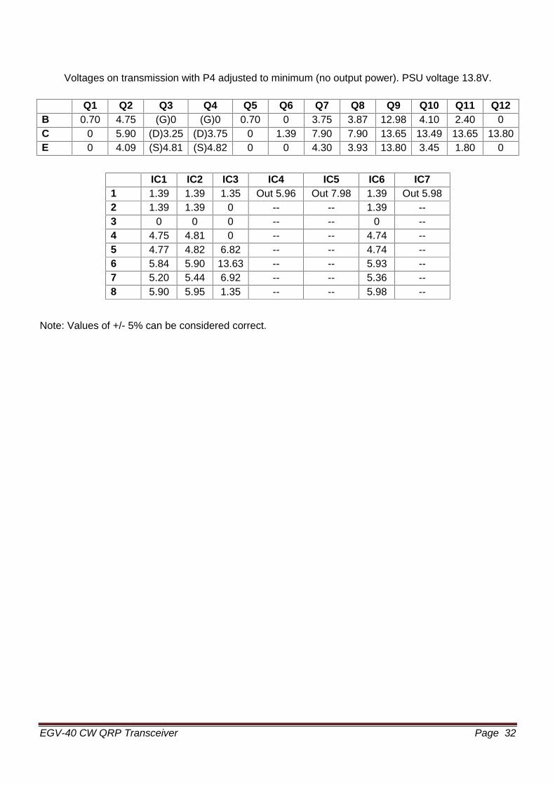
Voltages on transmission with P4 adjusted to minimum (no output power). PSU voltage 13.8V.
Q1 Q2 Q3 Q4 Q5 Q6 Q7 Q8 Q9 Q10 Q11 Q12B 0.70 4.75 (G)0 (G)0 0.70 0 3.75 3.87 12.98 4.10 2.40 0C 0 5.90 (D)3.25 (D)3.75 0 1.39 7.90 7.90 13.65 13.49 13.65 13.80E 0 4.09 (S)4.81 (S)4.82 0 0 4.30 3.93 13.80 3.45 1.80 0
IC1 IC2 IC3 IC4 IC5 IC6 IC71 1.39 1.39 1.35 Out 5.96 Out 7.98 1.39 Out 5.982 1.39 1.39 0 -- -- 1.39 --3 0 0 0 -- -- 0 --4 4.75 4.81 0 -- -- 4.74 --5 4.77 4.82 6.82 -- -- 4.74 --6 5.84 5.90 13.63 -- -- 5.93 --7 5.20 5.44 6.92 -- -- 5.36 --8 5.90 5.95 1.35 -- -- 5.98 --
Note: Values of +/- 5% can be considered correct.

EGV-40 CW QRP Transceiver Page 33
Limited WARRANTYPlease read carefully BEFORE building your kit
All parts and hardware supplied with the kit are under warranty in case of manufacturing defect for theperiod of one year after sale. The warranty does not include the transmitter power amplifier transistor.
The original purchaser has the option of examining the kit and manual for 10 days. If, within this period,the buyer decides not to build the kit, he or she may return the entire unassembled kit at their ownexpense Shipping charges included on the kit price and sale commissions (by banks or “Paypal”, etc)won't be returned..Please, BEFORE making a return, ask for directions by email to: ea3gcy@gmail.
Javier Solans, ea3gcy, warrants this device to function as described in this documentation provided thatit is assembled and used correctly according to all printed instructions.It is your responsibility to follow all directions in the instruction manual, to identify parts correctly, and touse good workmanship and proper tools and instruments in constructing and adjusting this kit.REMEMBER: This kit will not work as a commercially manufactured set, however, can often give similarresults. Do not expect great performance, but it is sure that you will have a lot of fun!
If you notice a missing kit part missing, please do first a thorough inventory. Check all bags, envelopesor boxes carefully. If need be, email me and I will promptly replace any missing part. Even in the casethat you find the exact replacement locally, please let us know so we are aware of the problem and getready to help other customers.I can also supply any part that you have lost or break accidentally.If you find any errors in this manual or would like to make a comment, please do not hesitate incontacting me at: [email protected]
THANKS for building the EGV-40 CW transceiver kit.Enjoy QRP!73 Javier Solans, ea3gcy

EGV-40 CW QRP Transceiver Page 34
SCHEMATICS

EGV-40 CW QRP Transceiver Page 35
WIRING
The EGV-40 wiring is very simple:-For the antenna connection use RF-rated fine coaxial cable such as RG-174 or similar.-If you place the polyvaricon outboard, use short and rigid wires as the mechanical stability is important.-A metal box is highly recommended
Take notice that the EGV-40 is NOT PROTECTED against polarity inversions!It is a good idea to place a diode (ex. BY255 or larger) in parallel with the PSU input on the EGV-40. Thecathode (the end with the printed band) goes to the positive wire. If your PSU supports shortcircuits orhas a fuse on its output, OK; else you will need to buy or build a cable with an on-line fuse in series.