training quectel
TRANSCRIPT

Wireless Module Expert
Quectel Wireless Solutions
Kavin He
www.quectel.com
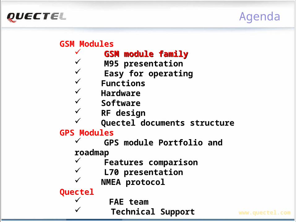
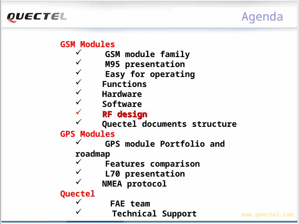
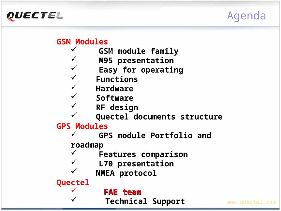
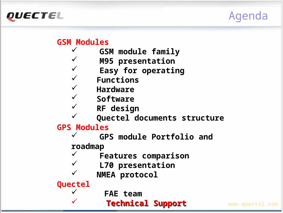
Agenda
GSM Modules GSM module family GSM module family M95 presentation Easy for operating Functions Hardware Software RF design Quectel documents structure
GPS Modules GPS module Portfolio and roadmap Features comparison L70 presentation NMEA protocol
Quectel FAE team Technical Support
www.quectel.com
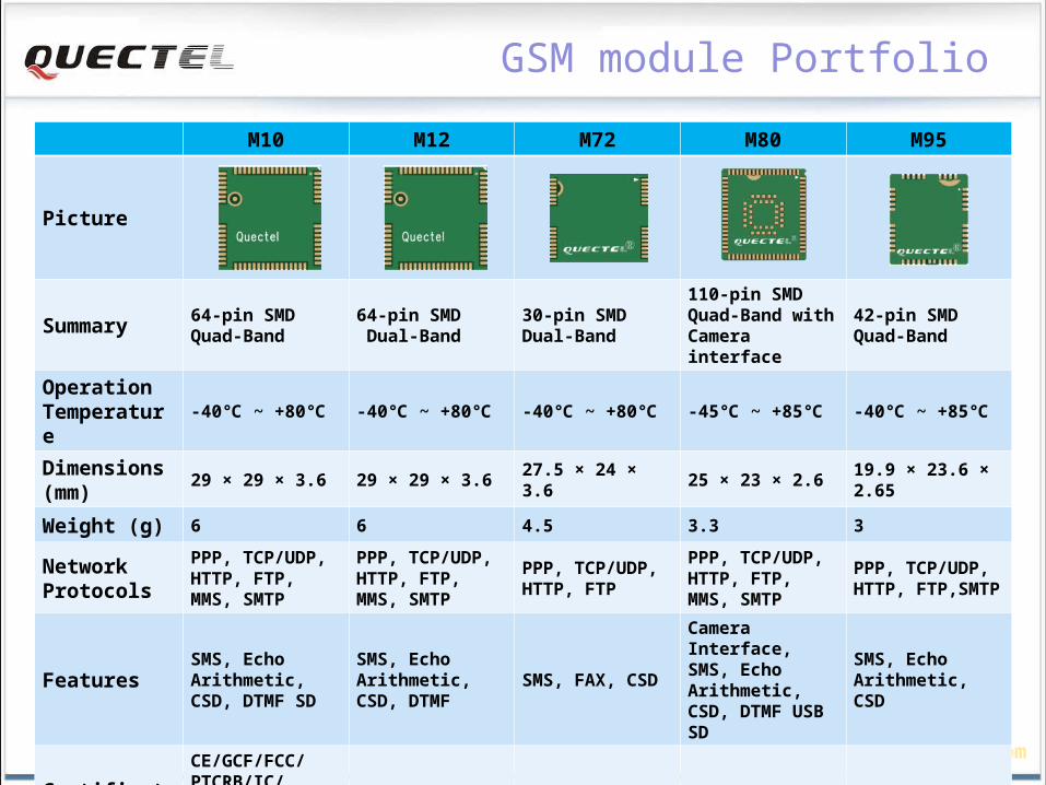
GSM module Portfolio
M10 M12 M72 M80 M95
Picture
Summary64-pin SMD Quad-Band
64-pin SMD Dual-Band
30-pin SMD Dual-Band
110-pin SMDQuad-Band with Camera interface
42-pin SMD Quad-Band
Operation Temperature
-40℃ ~ +80℃ -40℃ ~ +80℃ -40℃ ~ +80℃ -45℃ ~ +85℃ -40℃ ~ +85℃
Dimensions (mm)
29 × 29 × 3.6 29 × 29 × 3.6 27.5 × 24 × 3.6 25 × 23 × 2.6 19.9 × 23.6 × 2.65
Weight (g) 6 6 4.5 3.3 3
Network Protocols
PPP, TCP/UDP, HTTP, FTP, MMS, SMTP
PPP, TCP/UDP, HTTP, FTP, MMS, SMTP
PPP, TCP/UDP, HTTP, FTP
PPP, TCP/UDP, HTTP, FTP, MMS, SMTP
PPP, TCP/UDP, HTTP, FTP,SMTP
FeaturesSMS, Echo Arithmetic, CSD, DTMF SD
SMS, Echo Arithmetic, CSD, DTMF
SMS, FAX, CSD
Camera Interface, SMS, Echo Arithmetic, CSD, DTMF USB SD
SMS, Echo Arithmetic, CSD
Certifications
CE/GCF/FCC/PTCRB/IC/ANATEL/NORM/ TACOFETEL/ICASA/NCC
CE CE CE/ICASA/ CE/FCC/IC/NCC

www.quectel.com
Agenda
GSM Modules GSM module family M95 presentationM95 presentation Easy for operating Functions Hardware Software RF design Quectel documents structure
GPS Modules GPS module Portfolio and roadmap Features comparison L70 presentation NMEA protocol
Quectel FAE team Technical Support
www.quectel.com
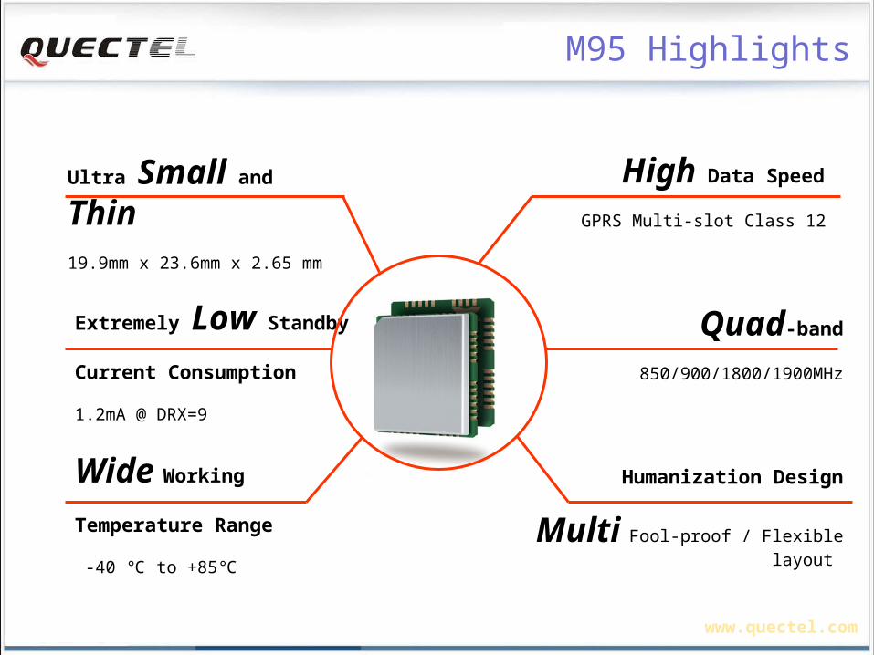
Ultra Small and Thin19.9mm x 23.6mm x 2.65 mm
High Data Speed
GPRS Multi-slot Class 12
Wide Working
Temperature Range
-40 ℃ to +85℃
Extremely Low Standby
Current Consumption
1.2mA @ DRX=9
M95 Highlights
Quad-band
850/900/1800/1900MHz
Humanization Design
Multi Fool-proof / Flexible layout
www.quectel.com
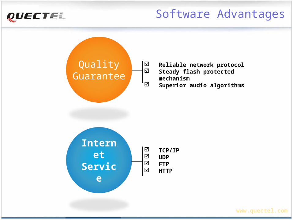
Reliable network protocol Steady flash protected mechanism Superior audio algorithms
Software Advantages
QualityGuarantee
InternetService
TCP/IP UDP FTP HTTP
www.quectel.com
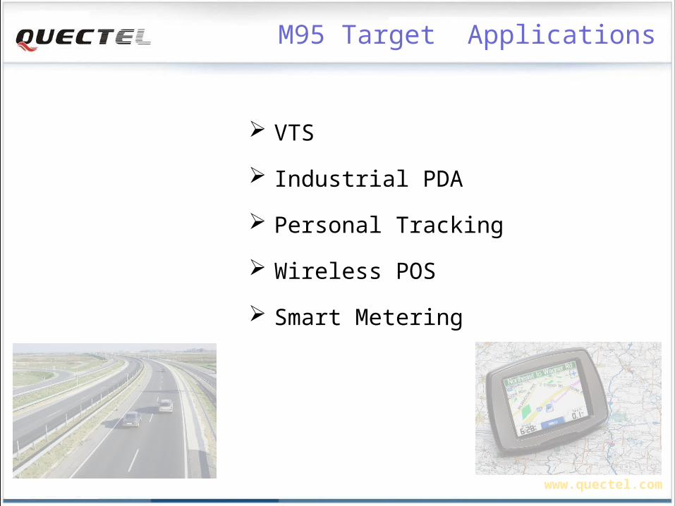
M95 Target Applications
VTS
Industrial PDA
Personal Tracking
Wireless POS
Smart Metering
www.quectel.com
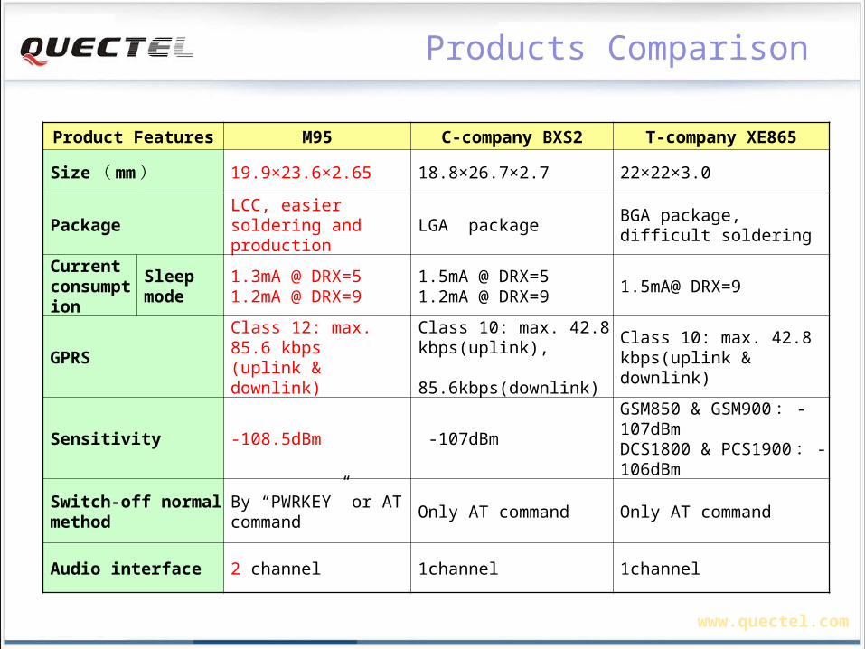
Products Comparison
Product Features M95 C-company BXS2 T-company XE865
Size ( mm) 19.9×23.6×2.65 18.8×26.7×2.7 22×22×3.0
PackageLCC, easier soldering and production
LGA packageBGA package, difficult soldering
Current consumption
Sleep mode
1.3mA @ DRX=51.2mA @ DRX=9
1.5mA @ DRX=51.2mA @ DRX=9
1.5mA@ DRX=9
GPRSClass 12: max. 85.6 kbps(uplink & downlink)
Class 10: max. 42.8 kbps(uplink), 85.6kbps(downlink)
Class 10: max. 42.8 kbps(uplink & downlink)
Sensitivity -108.5dBm -107dBm
GSM850 & GSM900 : -107dBmDCS1800 & PCS1900 : -106dBm
Switch-off normal method
By “PWRKEY” or AT command
Only AT command Only AT command
Audio interface 2 channel 1channel 1channel
www.quectel.com
Agenda
GSM Modules GSM module family M95 presentation Easy for operatingEasy for operating Functions Hardware Software RF design Quectel documents structure
GPS Modules GPS module Portfolio and roadmap Features comparison L70 presentation NMEA protocol
Quectel FAE team Technical Support
www.quectel.com
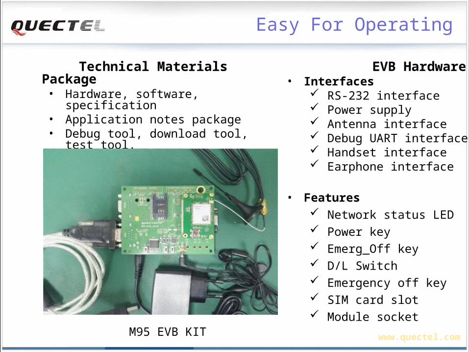
Easy For Operating
Technical Materials Package• Hardware, software, specification • Application notes package• Debug tool, download tool, test tool, EVB package• Approvals & test report package
M95 EVB KIT
EVB Hardware • Interfaces
RS-232 interface Power supply Antenna interface Debug UART interface Handset interface Earphone interface
• Features Network status LED Power key Emerg_Off key D/L Switch Emergency off key SIM card slot Module socket
www.quectel.com
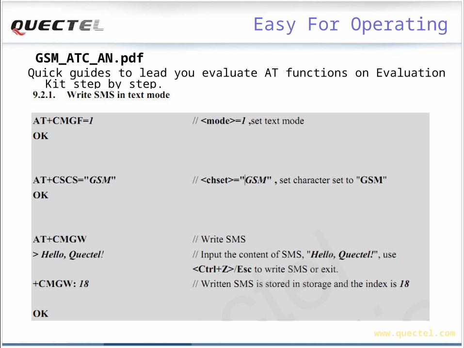
GSM_ATC_AN.pdfQuick guides to lead you evaluate AT functions on Evaluation Kit step by step.
Easy For Operating
www.quectel.com
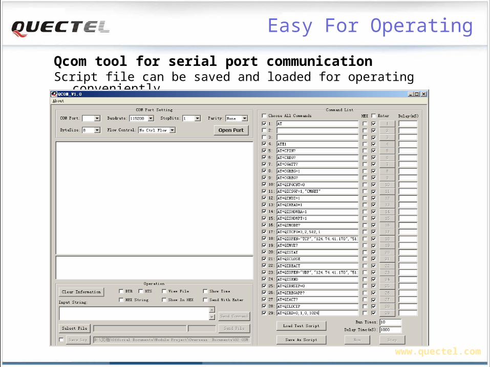
Qcom tool for serial port communicationScript file can be saved and loaded for operating conveniently.
Easy For Operating
www.quectel.com
Agenda
GSM Modules GSM module family M95 presentation Easy for operating FunctionsFunctions Hardware Software RF design Quectel documents structure
GPS Modules GPS module Portfolio and roadmap Features comparison L70 presentation NMEA protocol
Quectel FAE team Technical Support
www.quectel.com
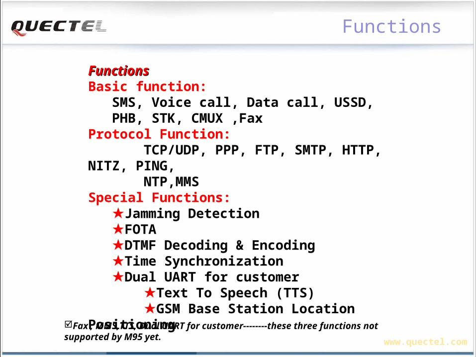
Functions
FunctionsFunctionsBasic function:
SMS, Voice call, Data call, USSD, PHB, STK, CMUX ,Fax
Protocol Function: TCP/UDP, PPP, FTP, SMTP, HTTP, NITZ, PING, NTP,MMS Special Functions:
★Jamming Detection★FOTA★DTMF Decoding & Encoding★Time Synchronization★Dual UART for customer
★Text To Speech (TTS) ★GSM Base Station Location Positioning
Fax , MMS,TTS, Dual UART for customer--------these three functions not supported by M95 yet.
www.quectel.com
TCPIP
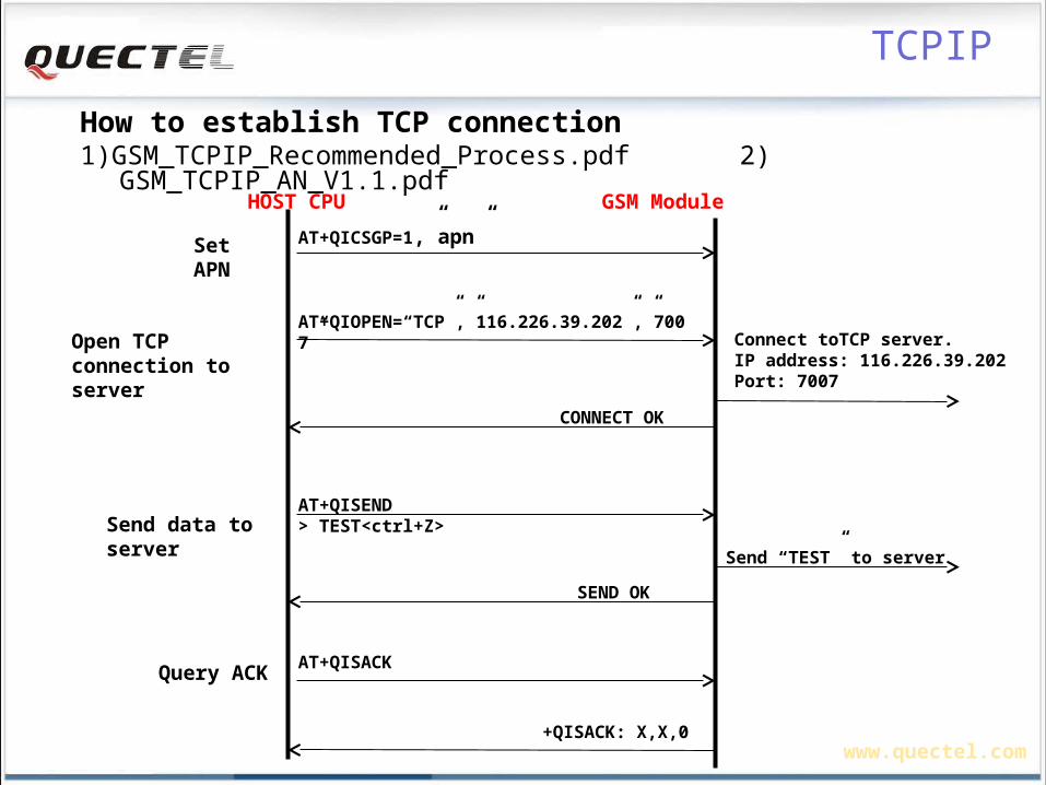
How to establish TCP connection1)GSM_TCPIP_Recommended_Process.pdf 2) GSM_TCPIP_AN_V1.1.pdf
HOST CPU GSM Module
AT+QICSGP=1,”apn”Set APN
AT+QIOPEN=“TCP”,”116.226.39.202”,”7007”Open TCP connection to server
Connect toTCP server. IP address: 116.226.39.202Port: 7007
CONNECT OK
AT+QISEND> TEST<ctrl+Z>
AT+QISACK
Send “TEST” to server
SEND OK
Query ACK
Send data to server
+QISACK: X,X,0
www.quectel.com
TCPIP
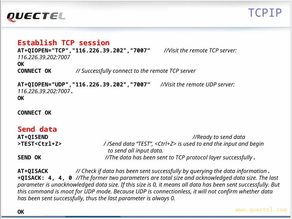
Establish TCP sessionAT+QIOPEN="TCP","116.226.39.202","7007“ //Visit the remote TCP server: 116.226.39.202:7007OKCONNECT OK // Successfully connect to the remote TCP server
AT+QIOPEN="UDP","116.226.39.202","7007“ //Visit the remote UDP server: 116.226.39.202:7007.OK CONNECT OK
Send dataAT+QISEND //Ready to send data>TEST<Ctrl+Z> / /Send data “TEST”, <Ctrl+Z> is used to end the input and begin to send all input data.SEND OK //The data has been sent to TCP protocol layer successfully.
AT+QISACK // Check if data has been sent successfully by querying the data information.+QISACK: 4, 4, 0 //The former two parameters are total size and acknowledged data size. The last parameter is unacknowledged data size. If this size is 0, it means all data has been sent successfully. But this command is moot for UDP mode. Because UDP is connectionless, it will not confirm whether data has been sent successfully, thus the last parameter is always 0. OK
www.quectel.com
TCPIP
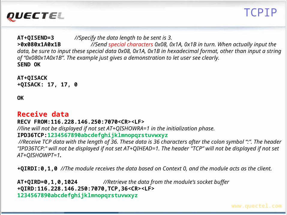
AT+QISEND=3 //Specify the data length to be sent is 3.>0x080x1A0x1B //Send special characters 0x08, 0x1A, 0x1B in turn. When actually input the data, be sure to input these special data 0x08, 0x1A, 0x1B in hexadecimal format, other than input a string of “0x080x1A0x1B”. The example just gives a demonstration to let user see clearly. SEND OK AT+QISACK+QISACK: 17, 17, 0 OK
Receive dataRECV FROM:116.228.146.250:7070<CR><LF>//line will not be displayed if not set AT+QISHOWRA=1 in the initialization phase.IPD36TCP:1234567890abcdefghijklmnopqrstuvwxyz //Receive TCP data with the length of 36. These data is 36 characters after the colon symbol “:”. The header "IPD36TCP:" will not be displayed if not set AT+QIHEAD=1. The header "TCP” will not be displayed if not set AT+QISHOWPT=1.
+QIRDI:0,1,0 //The module receives the data based on Context 0, and the module acts as the client.
AT+QIRD=0,1,0,1024 //Retrieve the data from the module’s socket buffer+QIRD:116.228.146.250:7070,TCP,36<CR><LF>1234567890abcdefghijklmnopqrstuvwxyz
www.quectel.com
TCPIP
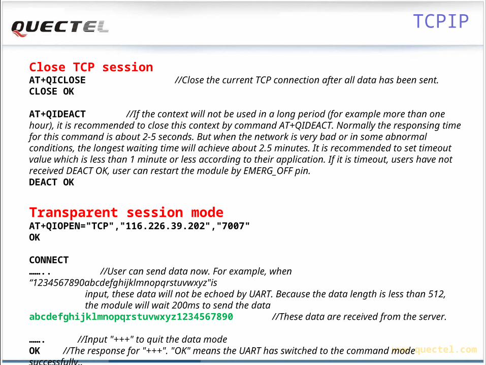
Close TCP sessionAT+QICLOSE //Close the current TCP connection after all data has been sent.CLOSE OK AT+QIDEACT //If the context will not be used in a long period (for example more than one hour), it is recommended to close this context by command AT+QIDEACT. Normally the responsing time for this command is about 2-5 seconds. But when the network is very bad or in some abnormal conditions, the longest waiting time will achieve about 2.5 minutes. It is recommended to set timeout value which is less than 1 minute or less according to their application. If it is timeout, users have not received DEACT OK, user can restart the module by EMERG_OFF pin. DEACT OK
Transparent session modeAT+QIOPEN="TCP","116.226.39.202","7007"OK CONNECT…….. //User can send data now. For example, when “1234567890abcdefghijklmnopqrstuvwxyz"is input, these data will not be echoed by UART. Because the data length is less than 512, the module will wait 200ms to send the dataabcdefghijklmnopqrstuvwxyz1234567890 //These data are received from the server.
……. //Input "+++" to quit the data modeOK //The response for "+++". "OK" means the UART has switched to the command mode successfully..
www.quectel.com
TCPIP
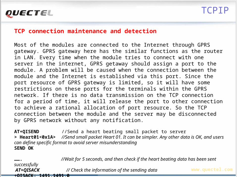
TCP connection maintenance and detection
Most of the modules are connected to the Internet through GPRS gateway. GPRS gateway here has the similar functions as the router in LAN. Every time when the module tries to connect with one server in the internet, GPRS getaway should assign a port to the module. A problem will be caused when the connection between the module and the Internet is established via this port. Since the port resource of GPRS gateway is limited, so it will have some restrictions on these ports for the terminals within the GPRS network. If there is no data transmission on the TCP connection for a period of time, it will release the port to other connection to achieve a rational allocation of port resource. So the TCP connection between the module and the server may be disconnected by GPRS network without any notification.
AT+QISEND //Send a heart beating small packet to server> Heart01<0x1A> //Send small packet Heart 01. It can be simpler. Any other data is OK, and users can define specific format to avoid server misunderstandingSEND OK ……. //Wait for 5 seconds, and then check if the heart beating data has been sent successfully AT+QISACK // Check the information of the sending data+QISACK: 1491,1491,0
www.quectel.com
SMS
Send/Receive a SMS in text mode
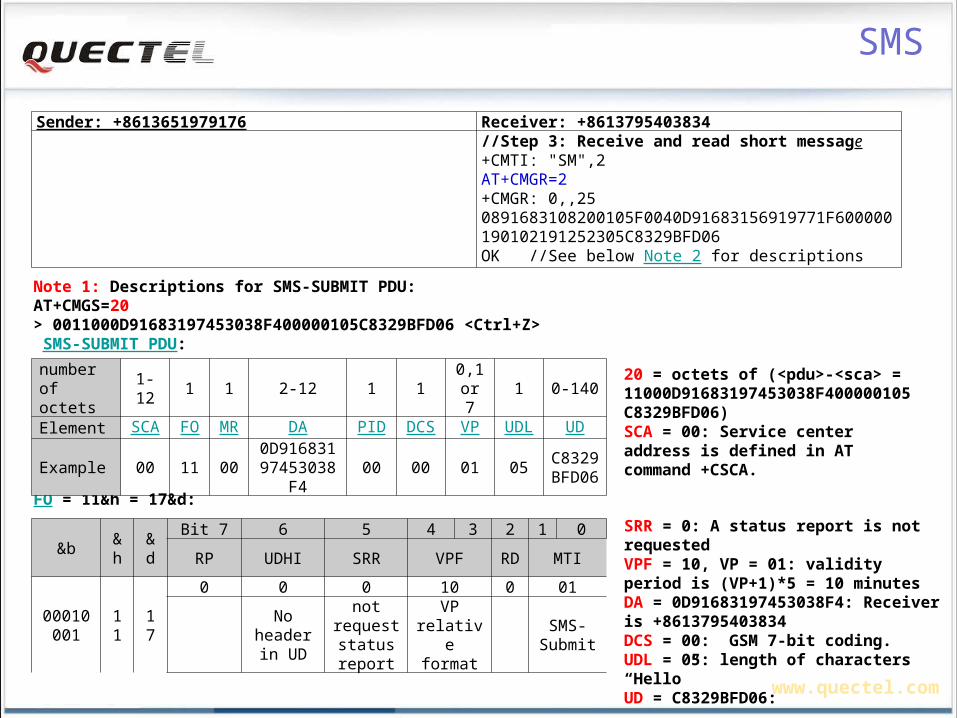
Sender: +8613651979176 Receiver: +8613795403834
//Step 1: Check service center addressAT+CSCS=“GSM” //Set the character mode as GSM mode. OKAT+CSCA? //Check the address of short message service center. OK
//Step 1: Check service center address (same as step 1 of sender)AT+CSCS="GSM"OKAT+CSCA?+CSCA: "+8613800210500",145OK
//Step 2: Set for sending English short message in text modeAT+CMGF=1 // Set the short message mode as TEXT mode:OKAT+CSCS=“GSM”OKAT+CSMP=17,167,0,241 // Set the related parameters for sending short message in text mode: FO, VP, PID and DCS2. DCS and +CSCS should match each other. To send English message, set +CSCS as “GSM” and <dcs> as GSM 7-bit coding.OKAT+CNMI=2,1,0,0,0 // Not require status report: <FO> of +CSMP = 17 or <ds> of +CNMI =0OK
//Step 2: Set for receiving English short message in text modeAT+CMGF=1 // Set the short message mode as TEXT mode:OKAT+CSCS=“GSM” //Set the character mode as GSM mode. If it sets as “UCS, the message content will be displayed in UCS2 format.OKAT+CNMI=2,1,0,0,0 // Set parameters for new message indication. 1 – get indication +CMTIOKAT+CPMS? //Check if short message storage is full. If it has been full, delete some messages by AT command +CMGD or +QMGDA.+CPMS: "SM",0,50,"SM",0,50,"SM",0,50OKAT+CSDH=1 //More information will be displayed if it equals 1.OK
www.quectel.com
SMS
Sender: +8613651979176 Receiver: +8613795403834//Step 1: Check service center addressAT+CSCS=“GSM” //Set the character mode as GSM mode. OKAT+CSCA? //Check the address of short message service center. For china mobile in , the CSA is "+8613800210500". If this address is wrong, the short message can NOT be sent successfully. And so this address should be set to the correct one by AT+CSCA=<sca> and save it by AT+CSAS.1 +CSCA: "+8613800210500",145OK
//Step 1: Check service center address (same as step 1 of sender)AT+CSCS="GSM"OKAT+CSCA?+CSCA: "+8613800210500",145OK
//Step 2: Set for sending English short message in text modeAT+CMGF=1 // Set the short message mode as TEXT mode:OKAT+CSCS=“GSM” // (Optional because it has been set in above step 1). Set the character mode as GSM mode.OKAT+CSMP=17,167,0,241 // Set the related parameters for sending short message in text mode: FO, VP, PID and DCS2. DCS and +CSCS should match each other. To send English message, set +CSCS as “GSM” and <dcs> as GSM 7-bit coding.OKAT+CNMI=2,1,0,0,0 // Not require status report: <FO> of +CSMP = 17 or <ds> of +CNMI =0OK
//Step 2: Set for receiving English short message in text modeAT+CMGF=1 // Set the short message mode as TEXT mode:OKAT+CSCS=“GSM” //Set the character mode as GSM mode. If it sets as “UCS, the message content will be displayed in UCS2 format.OKAT+CNMI=2,1,0,0,0 // Set parameters for new message indication. 1 – get indication +CMTIOKAT+CPMS? //Check if short message storage is full. If it has been full, delete some messages by AT command +CMGD or +QMGDA.+CPMS: "SM",0,50,"SM",0,50,"SM",0,50OKAT+CSDH=1 //More information will be displayed if it equals 1.OK

www.quectel.com
SMS
Sender: +8613651979176 Receiver: +8613795403834
//Step 3: Send English short message AT+CMGS="13795403834" // Send SMS: Enter the mobile phone number directly. Enter message content after “>” and end the input by pressing Ctrl and “Z” simultaneously.>Hello<Ctrl+Z>+CMGS: 140OK
//Step 3: Receive and read short message+CMTI: "SM",1AT+CMGR=1+CMGR: "REC UNREAD","+8613651979176","","2010/09/01 11:11:47+32",145,4,0,241,"+8613800210500",145,5HelloOKAT+CSCS="UCS2" //if set character set as “UCS, the message content will be displayed in UCS2 format.OKAT+CMGR=1+CMGR: "REC READ","002B0038003600310033003600350031003900370039003100370036","","2010/09/01 11:11:47+32",145,4,0,241,"002B0038003600310033003800300030003200310030003500300030",145,5OK
www.quectel.com
SMS
Send/Receive a SMS in PDU modeSender: +8613651979176 Receiver: +8613795403834//Step 1: Check service center addressAT+CSCS=“GSM” //Set the character mode as GSM mode. OKAT+CSCA? //Check the address of short message service center. For china mobile in , the CSA is "+8613800210500". If this address is wrong, the short message can NOT be sent successfully. And so this address should be set to the correct one by AT+CSCA=<sca> and save it by AT+CSAS. +CSCA: "+8613800210500",145OK
//Step 1: Check service center address (same as step 1 of sender)AT+CSCS="GSM"OKAT+CSCA?+CSCA: "+8613800210500",145OK
//Step 2: Set PDU modeAT+CMGF=0 // Set the short message mode as PDU mode. OK
//Step 2: Set PDU mode and parameters for receiving messagesAT+CMGF=0 //Set the short message mode as PDU mode.OKAT+CNMI=2,1,0,0,0 // Set parameters for new message indication. 1 – get indication +CMTIOKAT+CPMS? //Check if short message storage is full. If it has been full, delete some messages by AT command +CMGD or +QMGDA.+CPMS: "SM",1,50,"SM",1,50,"SM",1,50OK
//Step 3: Send English short message AT+CMGS=20 > 0011000D91683197453038F8329BFD06 <Ctrl+Z>+CMGS: 146OK //See below Note 1 for descriptions
www.quectel.com
SMS
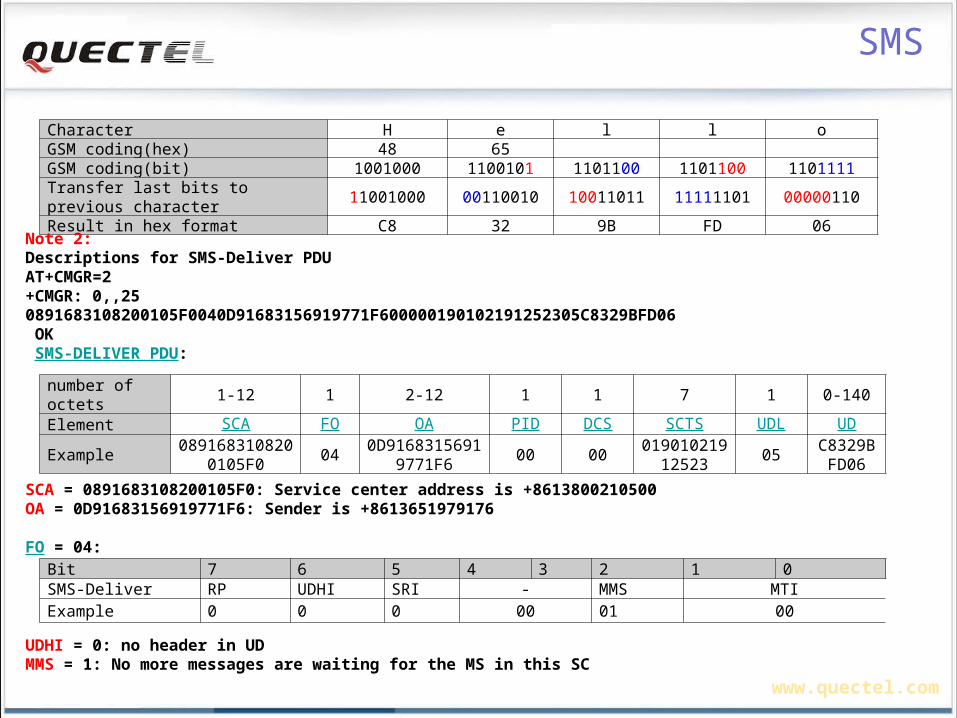
Sender: +8613651979176 Receiver: +8613795403834//Step 3: Receive and read short message+CMTI: "SM",2AT+CMGR=2+CMGR: 0,,250891683108200105F0040D91683156919771F600000190102191252305C8329BFD06OK //See below Note 2 for descriptions
Note 1: Descriptions for SMS-SUBMIT PDU:AT+CMGS=20 > 0011000D91683197453038F400000105C8329BFD06 <Ctrl+Z> SMS-SUBMIT PDU:
FO = 11&h = 17&d:
number of octets
1-12 1 1 2-12 1 10,1 or 7
1 0-140
Element SCA FO MR DA PID DCS VP UDL UD
Example 00 11 000D91683197453038F4
00 00 01 05C8329BFD0
6
&b&h
&d
Bit 7 6 5 4 3 2 1 0
RP UDHI SRR VPFRD
MTI
00010001
11 17
0 0 0 10 0 01
No header in
UD
not request status report
VP relative format
SMS-Submit
SRR = 0: A status report is not requestedVPF = 10, VP = 01: validity period is (VP+1)*5 = 10 minutesDA = 0D91683197453038F4: Receiver is +8613795403834DCS = 00: GSM 7-bit coding.UDL = 05: length of characters “Hello”UD = C8329BFD06:
20 = octets of (<pdu>-<sca> = 11000D91683197453038F400000105C8329BFD06)SCA = 00: Service center address is defined in AT command +CSCA.
www.quectel.com
SMS
Character H e l l oGSM coding(hex) 48 65GSM coding(bit) 1001000 1100101 1101100 1101100 1101111Transfer last bits to previous character 11001000 00110010 10011011 11111101 00000110Result in hex format C8 32 9B FD 06
Note 2: Descriptions for SMS-Deliver PDUAT+CMGR=2+CMGR: 0,,250891683108200105F0040D91683156919771F600000190102191252305C8329BFD06 OK SMS-DELIVER PDU:
SCA = 0891683108200105F0: Service center address is +8613800210500OA = 0D91683156919771F6: Sender is +8613651979176
FO = 04:
UDHI = 0: no header in UDMMS = 1: No more messages are waiting for the MS in this SC
number of octets
1-12 1 2-12 1 1 7 1 0-140
Element SCA FO OA PID DCS SCTS UDL UD
Example089168310820
0105F004
0D91683156919771F6
00 00019010219
1252305
C8329BFD06
Bit 7 6 5 4 3 2 1 0SMS-Deliver RP UDHI SRI - MMS MTIExample 0 0 0 00 01 00
www.quectel.com
SMS
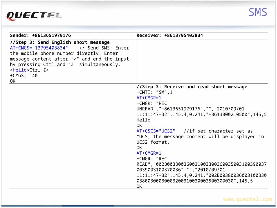
Sender: +8613651979176 Receiver: +8613795403834
//Step 3: Send English short message AT+CMGS="13795403834" // Send SMS: Enter the mobile phone number directly. Enter message content after “>” and end the input by pressing Ctrl and “Z” simultaneously.>Hello<Ctrl+Z>+CMGS: 140OK
//Step 3: Receive and read short message+CMTI: "SM",1AT+CMGR=1+CMGR: "REC UNREAD","+8613651979176","","2010/09/01 11:11:47+32",145,4,0,241,"+8613800210500",145,5HelloOKAT+CSCS="UCS2" //if set character set as “UCS, the message content will be displayed in UCS2 format.OKAT+CMGR=1+CMGR: "REC READ","002B0038003600310033003600350031003900370039003100370036","","2010/09/01 11:11:47+32",145,4,0,241,"002B0038003600310033003800300030003200310030003500300030",145,5OK
www.quectel.com
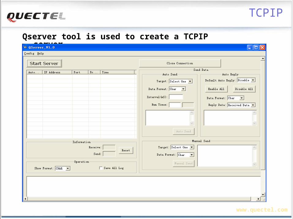
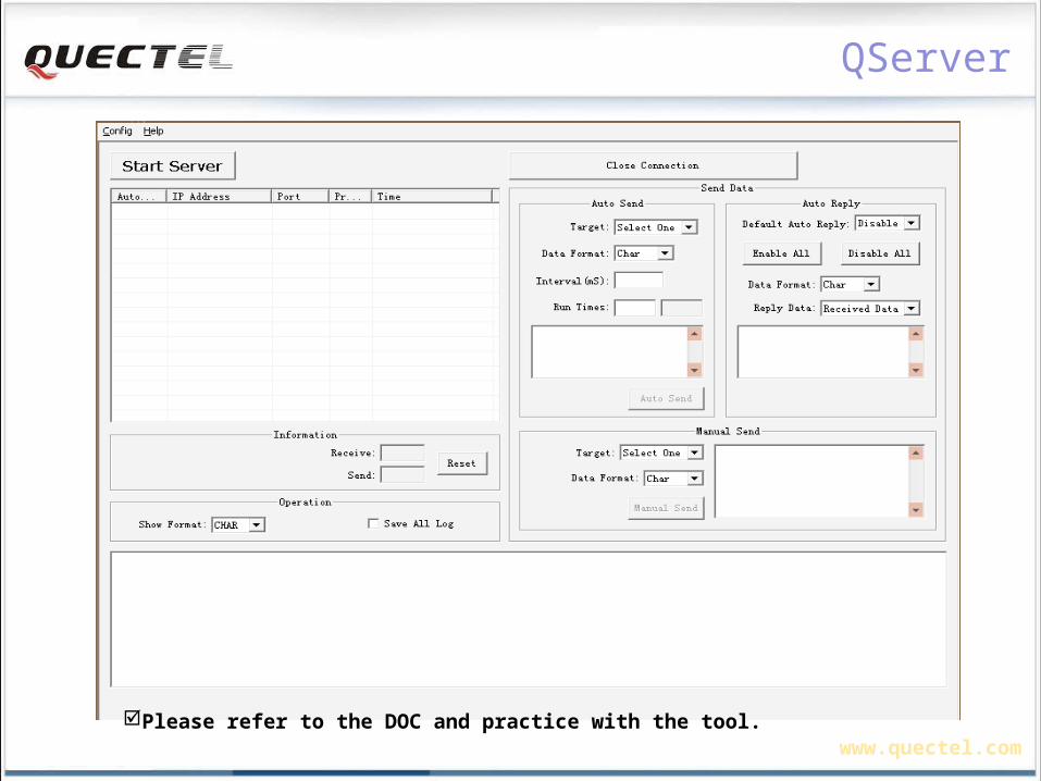
Qserver tool is used to create a TCPIP server.
TCPIP
www.quectel.com
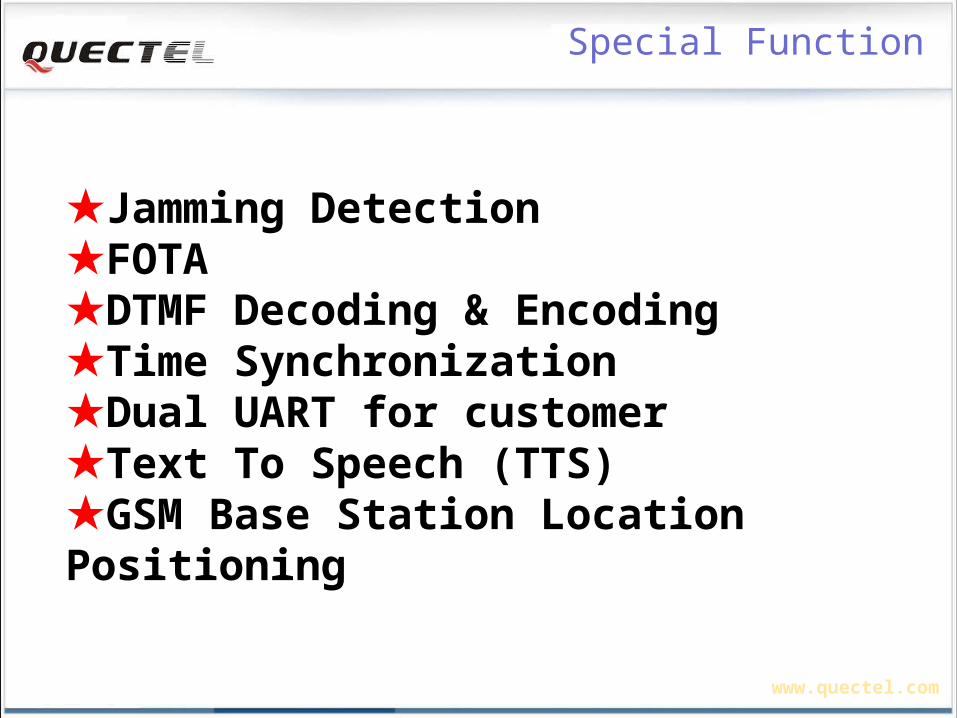
Special Function
★Jamming Detection★FOTA★DTMF Decoding & Encoding★Time Synchronization★Dual UART for customer★Text To Speech (TTS)★GSM Base Station Location Positioning
www.quectel.com
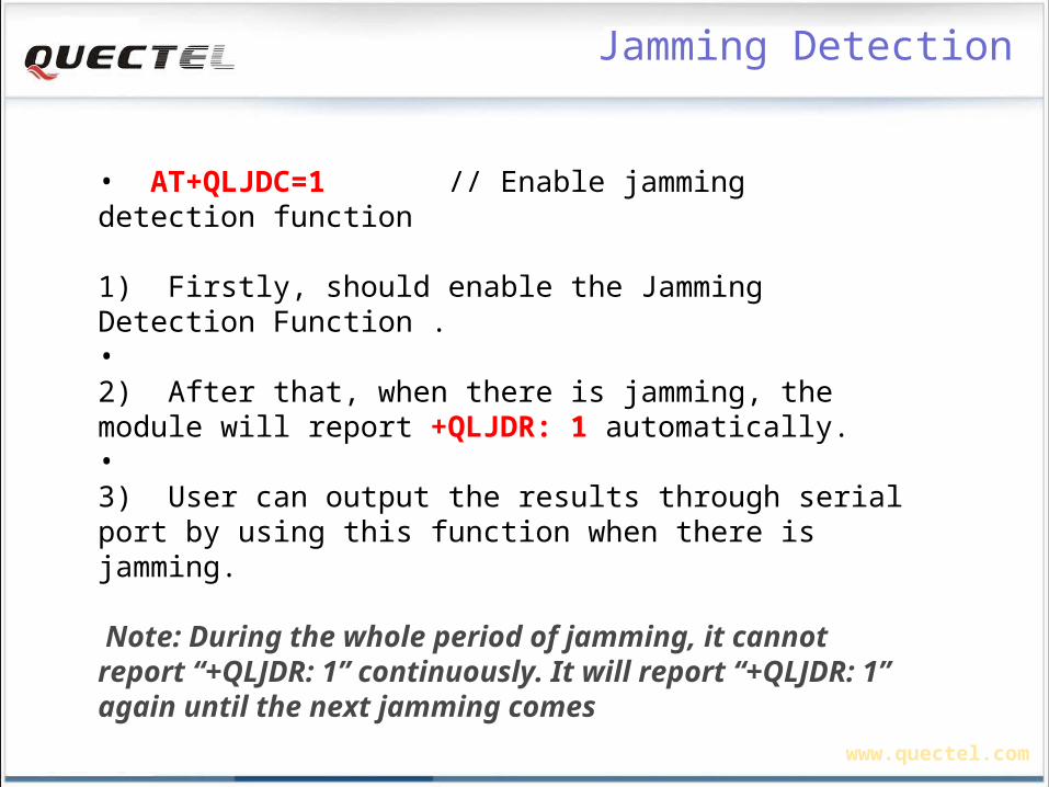
Jamming Detection
• AT+QLJDC=1 // Enable jamming detection function 1) Firstly, should enable the Jamming Detection Function .•2) After that, when there is jamming, the module will report +QLJDR: 1 automatically. •3) User can output the results through serial port by using this function when there is jamming.
Note: During the whole period of jamming, it cannot report “+QLJDR: 1” continuously. It will report “+QLJDR: 1” again until the next jamming comes
www.quectel.com
FOTA
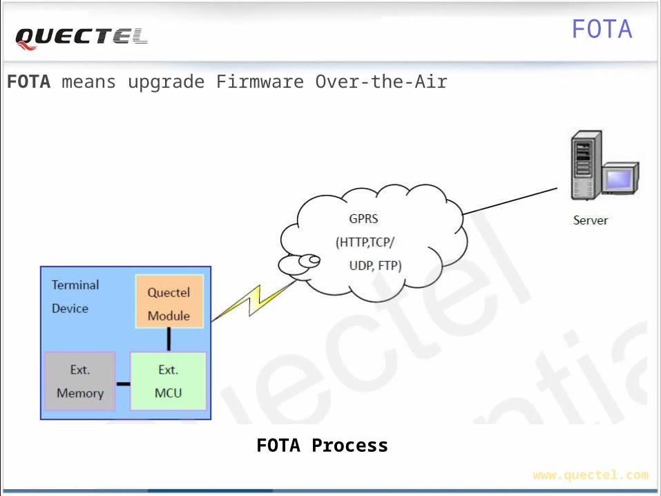
FOTA means upgrade Firmware Over-the-Air
FOTA Process
www.quectel.com
FOTA
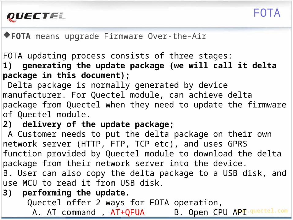
FOTA means upgrade Firmware Over-the-Air
FOTA updating process consists of three stages: 1) generating the update package (we will call it delta package in this document); Delta package is normally generated by device manufacturer. For Quectel module, can achieve delta package from Quectel when they need to update the firmware of Quectel module.2) delivery of the update package; A Customer needs to put the delta package on their own network server (HTTP, FTP, TCP etc), and uses GPRS function provided by Quectel module to download the delta package from their network server into the device.B. User can also copy the delta package to a USB disk, and use MCU to read it from USB disk.3) performing the update. Quectel offer 2 ways for FOTA operation, A. AT command , AT+QFUA B. Open CPU API
www.quectel.com
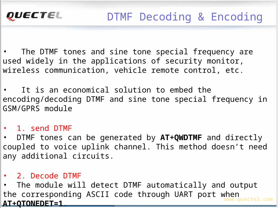
DTMF Decoding & Encoding
• The DTMF tones and sine tone special frequency are used widely in the applications of security monitor, wireless communication, vehicle remote control, etc.
• It is an economical solution to embed the encoding/decoding DTMF and sine tone special frequency in GSM/GPRS module
• 1. send DTMF• DTMF tones can be generated by AT+QWDTMF and directly coupled to voice uplink channel. This method doesn’t need any additional circuits.
• 2. Decode DTMF• The module will detect DTMF automatically and output the corresponding ASCII code through UART port when AT+QTONEDET=1.
www.quectel.com
Time Synchronization
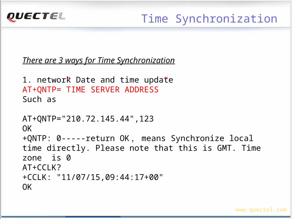
There are 3 ways for Time Synchronization
1. network Date and time updateAT+QNTP=”TIME SERVER ADDRESS”Such as
AT+QNTP="210.72.145.44",123OK+QNTP: 0-----return OK , means Synchronize local time directly. Please note that this is GMT. Time zone is 0AT+CCLK?+CCLK: "11/07/15,09:44:17+00"OK
www.quectel.com
Time Synchronization
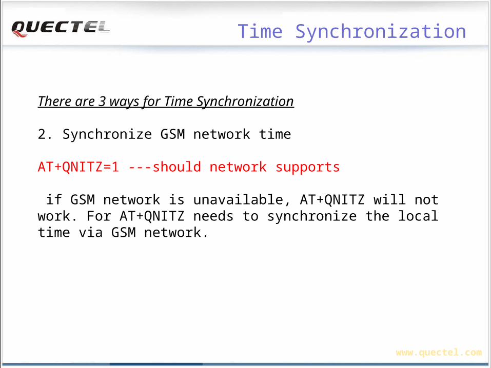
There are 3 ways for Time Synchronization
2. Synchronize GSM network time
AT+QNITZ=1 ---should network supports
if GSM network is unavailable, AT+QNITZ will not work. For AT+QNITZ needs to synchronize the local time via GSM network.
www.quectel.com
Time Synchronization
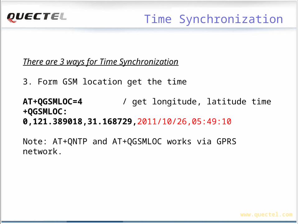
There are 3 ways for Time Synchronization
3. Form GSM location get the time
AT+QGSMLOC=4 / get longitude, latitude time+QGSMLOC: 0,121.389018,31.168729,2011/10/26,05:49:10
Note: AT+QNTP and AT+QGSMLOC works via GPRS network.
www.quectel.com
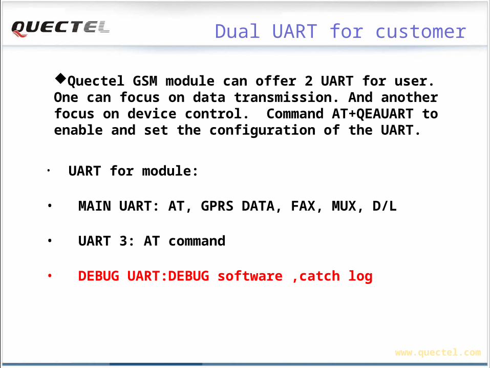
Dual UART for customer
Quectel GSM module can offer 2 UART for user. One can focus on data transmission. And another focus on device control. Command AT+QEAUART to enable and set the configuration of the UART.
• UART for module:
• MAIN UART: AT, GPRS DATA, FAX, MUX, D/L
• UART 3: AT command
• DEBUG UART:DEBUG software ,catch log
www.quectel.com
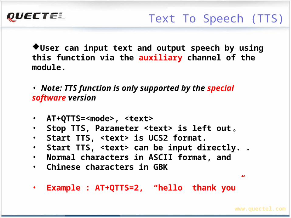
Text To Speech (TTS)
User can input text and output speech by using this function via the auxiliary channel of the module.
• Note: TTS function is only supported by the special software version
• AT+QTTS=<mode>, <text>• Stop TTS, Parameter <text> is left out。• Start TTS, <text> is UCS2 format.• Start TTS, <text> can be input directly. .• Normal characters in ASCII format, and • Chinese characters in GBK
• Example : AT+QTTS=2, “hello thank you”
www.quectel.com
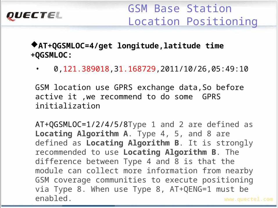
GSM Base Station Location Positioning
AT+QGSMLOC=4/get longitude,latitude time+QGSMLOC:
• 0,121.389018,31.168729,2011/10/26,05:49:10
GSM location use GPRS exchange data,So before active it ,we recommend to do some GPRS initialization
AT+QGSMLOC=1/2/4/5/8Type 1 and 2 are defined as Locating Algorithm A. Type 4, 5, and 8 are defined as Locating Algorithm B. It is strongly recommended to use Locating Algorithm B. The difference between Type 4 and 8 is that the module can collect more information from nearby GSM coverage communities to execute positioning via Type 8. When use Type 8, AT+QENG=1 must be enabled.
• Notice: we do not promote this function.
www.quectel.com
Agenda
GSM Modules GSM module family M95 presentation Easy for operating Functions Hardware Hardware Software RF design Quectel documents structure
GPS Modules GPS module Portfolio and roadmap Features comparison L70 presentation NMEA protocol
Quectel FAE team Technical Support
www.quectel.com
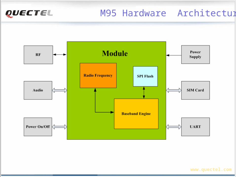
M95 Hardware Architecture
www.quectel.com
M95 Hardware Architecture
BB&RF
RF PAMSAW Filter
32KHz
26MHzRF Transceiver
RTC
GPIO
Serial Interface
SIM Interface
RF_ANT
VBAT
PWRKEY
EMERG_OFF
VRTC
Status&Netlight
UART
SIM Interface
Reset
ESD
PMU
MEMORYAudio Audio
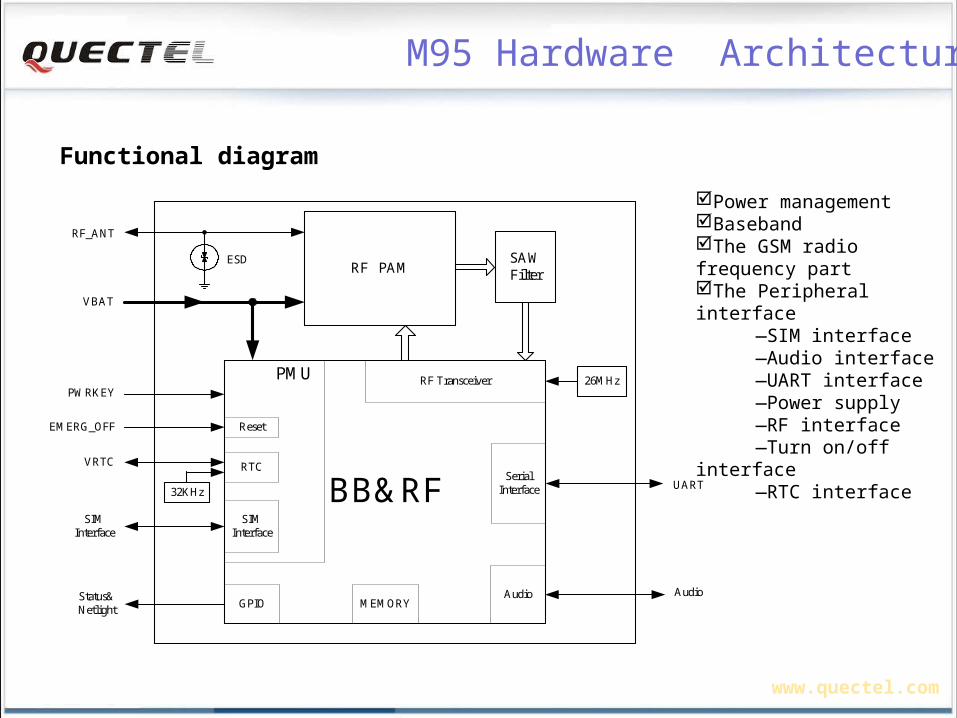
Functional diagram
Power managementBasebandThe GSM radio frequency partThe Peripheral interface
—SIM interface—Audio interface—UART interface—Power supply—RF interface—Turn on/off interface—RTC interface
www.quectel.com
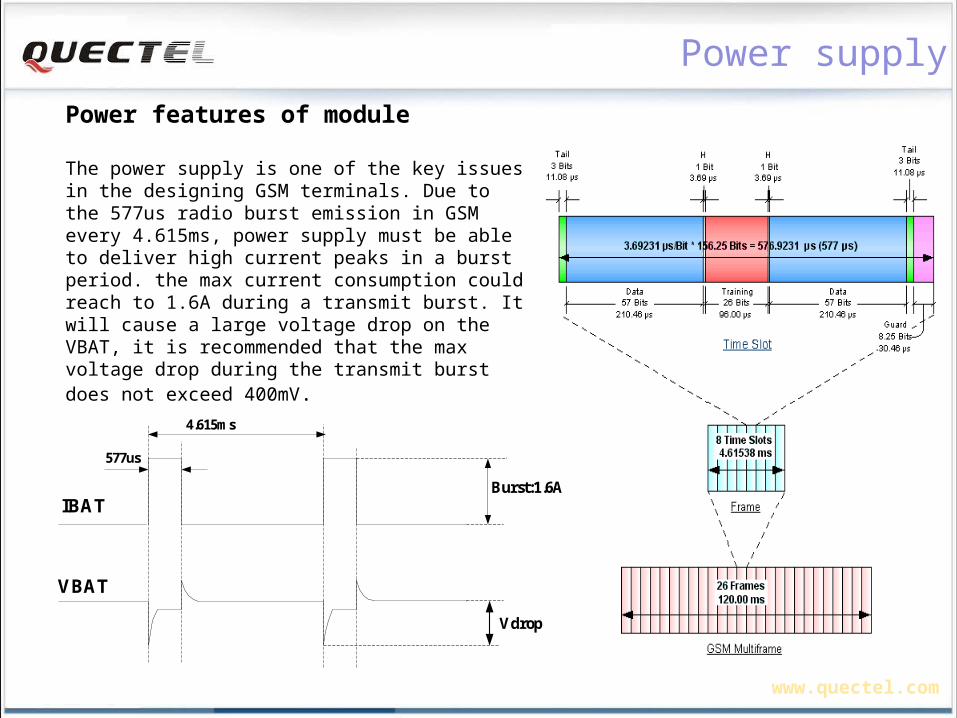
Power supply
Vdrop
4.615ms
577us
IBAT
VBAT
Burst:1.6A
Power features of module
The power supply is one of the key issues in the designing GSM terminals. Due to the 577us radio burst emission in GSM every 4.615ms, power supply must be able to deliver high current peaks in a burst period. the max current consumption could reach to 1.6A during a transmit burst. It will cause a large voltage drop on the VBAT, it is recommended that the max voltage drop during the transmit burst does not exceed 400mV.
www.quectel.com
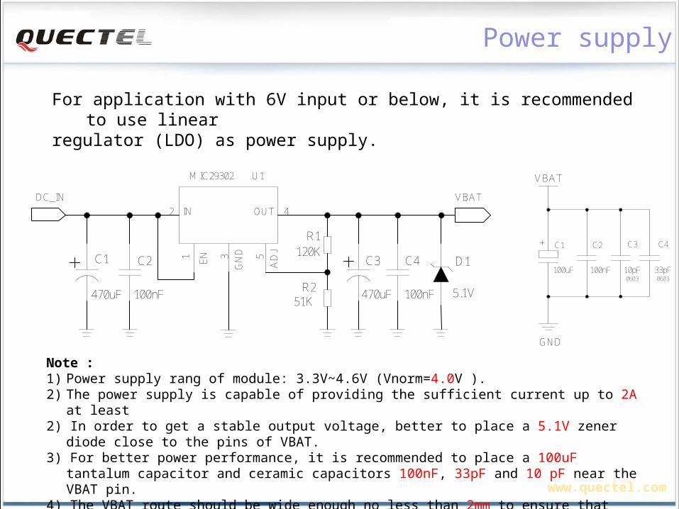
Note :1) Power supply rang of module: 3.3V~4.6V (Vnorm=4.0V ).2) The power supply is capable of providing the sufficient current up to 2A at least2) In order to get a stable output voltage, better to place a 5.1V zener diode close to the pins of
VBAT.3) For better power performance, it is recommended to place a 100uF tantalum capacitor and ceramic
capacitors 100nF, 33pF and 10 pF near the VBAT pin.4) The VBAT route should be wide enough no less than 2mm to ensure that there is not too much
voltage drop occurring during transmit burst and the Module’s GND trace should be as wider and shorter as possible.
DC_IN
C1 C2
MIC29302 U1
IN OUTE
N
GN
D
AD
J
2 4
1 3 5
VBAT
100nF
C3
470uF
C4
100nF
R1
D1120K
51KR2
470uF 5.1V
VBAT
C2C1+ C3 C4
GND
100uF 100nF 10pF0603
33pF0603
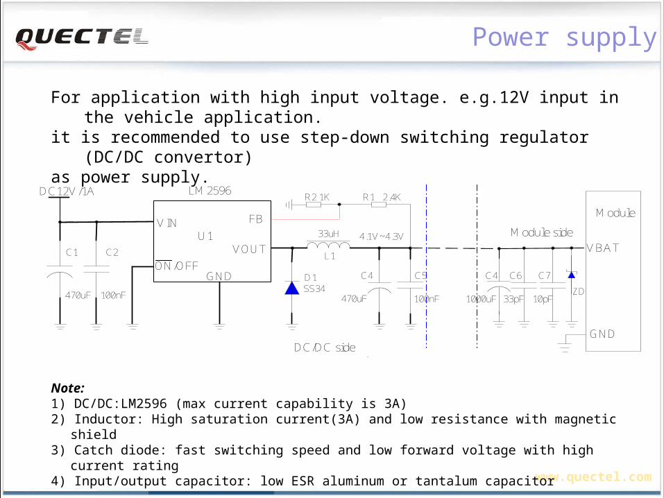
For application with 6V input or below, it is recommended to use linear regulator (LDO) as power supply.
Power supply
www.quectel.com
Note:1) DC/DC:LM2596 (max current capability is 3A)2) Inductor: High saturation current(3A) and low resistance with magnetic shield3) Catch diode: fast switching speed and low forward voltage with high current rating4) Input/output capacitor: low ESR aluminum or tantalum capacitor
For application with high input voltage. e.g.12V input in the vehicle application.it is recommended to use step-down switching regulator (DC/DC convertor) as power supply.
DC12V/1A
VIN
VOUT
GND
FBModule
VBAT
GND
470uF 100nF
C1
100nF
C2
R1R2
U1
C4 C5
4.1V~4.3V
470uF
ON/OFF
LM2596
D1
L1
33uH
2.4K1K
C6 C7
33pF 10pF
C4
1000uF
Module side
DC/DC side
ZDSS34
Power supply
www.quectel.com
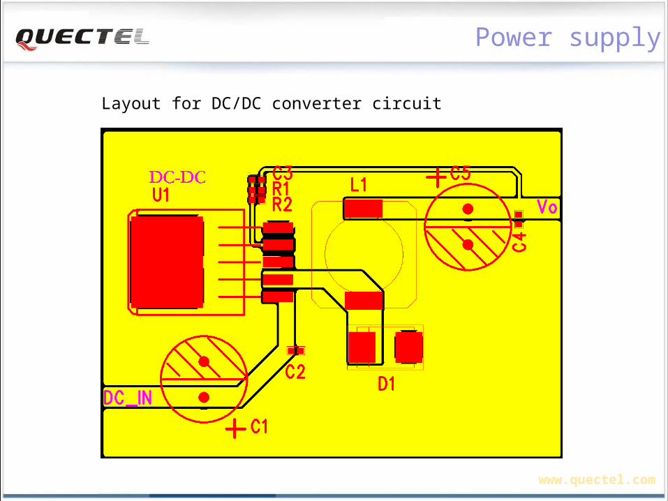
Layout for DC/DC converter circuit
Power supply
www.quectel.com
Power ON/OFF
Turn on the module using driving circuit
Turn on pulse
PWRKEY
4.7K
47K
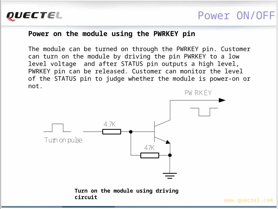
Power on the module using the PWRKEY pin
The module can be turned on through the PWRKEY pin. Customer can turn on the module by driving the pin PWRKEY to a low level voltage and after STATUS pin outputs a high level, PWRKEY pin can be released. Customer can monitor the level of the STATUS pin to judge whether the module is power-on or not.
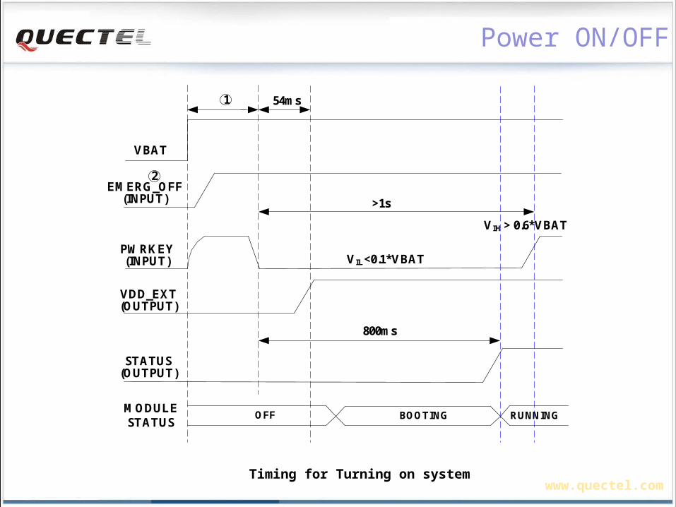
www.quectel.comTiming for Turning on system
VDD_EXT(OUTPUT)
VIL<0.1*VBAT
VIH > 0.6*VBAT
VBAT
PWRKEY(INPUT)
EMERG_OFF(INPUT)
54ms
STATUS(OUTPUT)
800ms
>1s
OFF BOOTINGMODULE STATUS
RUNNING
2
1
Power ON/OFF
www.quectel.comTiming of Turning of the module
VBAT
PWRKEY(INPUT)
STATUS(OUTPUT)
EMERG_OFF(INPUT)
Logout net about 2s to 12s
0.6s<Pulldown<1s >160us
Power ON/OFF
www.quectel.com
Reference circuit for EMERG_OFF by using driving circuit
Emergency shutdown pulse
EMERG_OFF
4.7K
47K
Emergency shutdown using EMERG_OFF pin
The module can be shut down by driving the pin EMERG_OFF to a low level voltage over 20ms and then releasing it. The EMERG_OFF line can be driven by an Open Drain / Collector driver or a button.
Notice:Be cautious to use the pin EMERG_OFF. It should only be used under emergent situation. For instance, if the module is unresponsive or abnormal, the pin EMERG_OFF could be used to shut down the system.
Power ON/OFF
www.quectel.com
SLEEP MODE
Sleep mode
The SLEEP mode is disabled in default software configuration. Customer’s applicationcan enable this mode by “AT+QSCLK=1”. When “AT+QSCLK=1” is sent to the module, customer’s application can control the module to enter or exit from the SLEEP mode through pin DTR. When DTR is set to high Level and not interrupter, the module will enter SLEEP mode automatically. In this mode,the module can still receive voice, SMS or GPRS paging from network but the UARTport is not accessible.
Wake up the module from SLEEP mode
When the module is in the SLEEP mode, the following methods can wake up the module1) If the DTR Pin is set low, it would wake up the module from the SLEEP mode. The UART port will be active within 20ms after DTR is changed to low level. 2) Receiving a voice or data call from network wakes up module.3) Receiving an SMS from network wakes up the module.
Note: DTR pin should be held low level during communication between the module and DTE. If the module does not act as 2) or 3) , few seconds later it will came into sleep mode again.
www.quectel.com
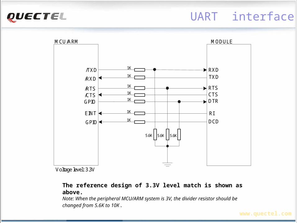
UART interface
Logic levels of UART port (VDD_EXT=2.8V)
The main features of main UART port:
1) Receive and transmit lines TXD and RXD, hardware flow control lines RTS and CTS, Other control lines DTR, DCD and RI.
2) The hardware flow control was disabled by default. AT command “AT+IFC=2,2” is used to enable hardware flow control.
3) Support the communication baud rate as the following: 300,600,1200,2400,4800,9600,14400,19200,28800,38400,57600,115200.4) The default setting is autobauding mode. Support the following baud rates forautobauding function: 4800, 9600, 19200, 38400, 57600, 115200.
Parameter Min Max Unit
VIL 0 0.25×VDD_EXT V
VIH 0.75×VDD_EXT VDD_EXT +0.3 V
VOL 0 0.15×VDD_EXT V
VOH 0.85×VDD_EXT VDD_EXT V
www.quectel.com
MCU/ARM MODULE
/TXD
/RXD TXDRXD
RTSCTSDTR
RI
/RTS/CTSGPIO
EINT
GPIO DCD
1K
1K
1K
1K
1K
1K
1K
5.6K 5.6K5.6K
Voltage level: 3.3V
The reference design of 3.3V level match is shown as above. Note: When the peripheral MCU/ARM system is 3V, the divider resistor should be changed from 5.6K to 10K.
UART interface
www.quectel.com
MCU/ARM
/TXD
/RXD
1K
VDD_EXT
4.7k
VCC_MCU
4.7k
4.7k
4.7k
VDD_EXT
TXD
RXD
RTS
CTS
DTR
RI
/RTS
/CTS
Voltage level: 5V
GPIO STATUS
MODULE
GPIO
EINT
VCC_MCU
5V level match circuit
UART interface
www.quectel.com
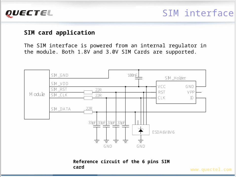
SIM interface
Reference circuit of the 6 pins SIM card
Module
SIM_VDD
SIM_GND
SIM_RST
SIM_CLK
SIM_DATA 22R
22R
22R
100nFSIM_Holder
GND
ESDA6V8V6
33pF 33pF 33pF
VCC
RST
CLK IO
VPP
GND
GND
33pF
SIM card application
The SIM interface is powered from an internal regulator in the module. Both 1.8V and 3.0V SIM Cards are supported.
www.quectel.com
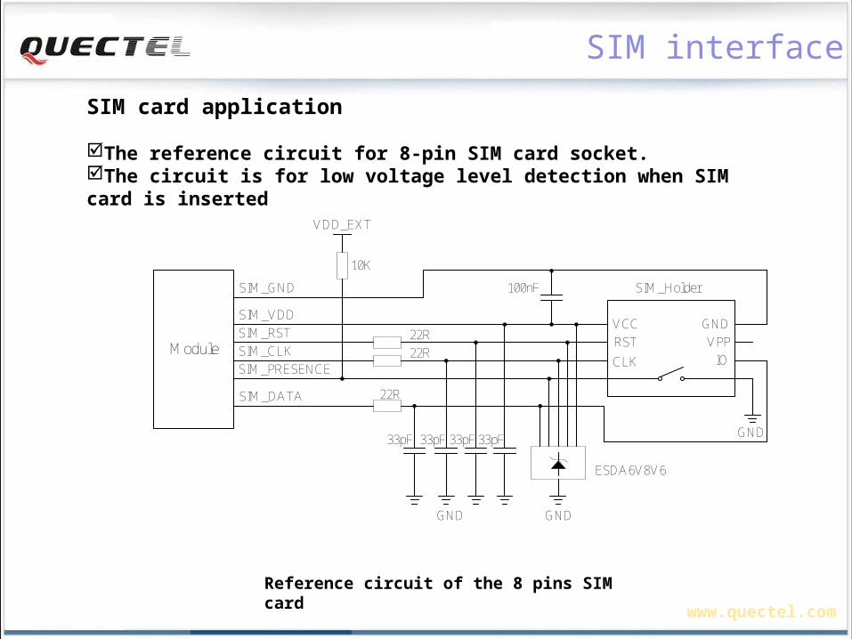
SIM interface
Reference circuit of the 8 pins SIM card
SIM card application
The reference circuit for 8-pin SIM card socket.The circuit is for low voltage level detection when SIM card is inserted
Module
SIM_VDD
SIM_GND
SIM_RST
SIM_CLK
SIM_DATA
SIM_PRESENCE
22R
22R
22R
VDD_EXT
10K
100nF SIM_Holder
GND
GND
ESDA6V8V6
33pF33pF 33pF 33pF
VCC
RST
CLK IO
VPP
GND
GND
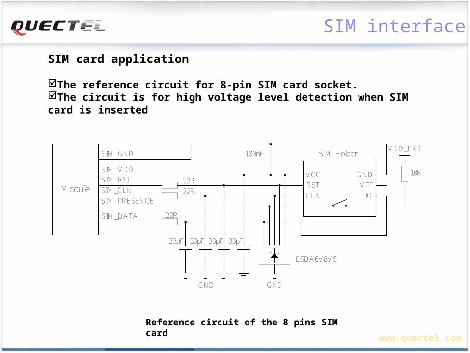
www.quectel.com
SIM interface
Reference circuit of the 8 pins SIM card
SIM card application
The reference circuit for 8-pin SIM card socket.The circuit is for high voltage level detection when SIM card is inserted
Module
SIM_VDD
SIM_GND
SIM_RST
SIM_CLK
SIM_DATA
SIM_PRESENCE
22R
22R
22R
10K
100nF SIM_Holder
GND
ESDA6V8V6
33pF33pF 33pF 33pF
VCC
RST
CLK IO
VPP
GND
GND
VDD_EXT
www.quectel.com
Notice for SIM interface Design
Place the SIM card holder close to module as close as possible. Ensure the trace length of SIM signals keeps less than 200mm.
1) Keep the SIM signals far away from VBAT power and RF trace.
2) The width of SIM_VDD and SIM_GND trace is not less than 0.5mm. Place a bypass capacitor close to SIM card power pin. The value of capacitor is less than 1uF.
3) To avoid possible cross-talk from the SIM_CLK signal to the SIM_DATA signal be careful that both traces are not placed closely next to each other. The traces of SIM_CLK, SIM_DATA and SIM_RST are recommended to be around with GND independently.
4) All signals of SIM interface should be protected against ESD with a TVS diode array. It is recommended to add TVS diode and The parasitic capacitance of TVS diode is less than 50pF.
5) The 22Ω resistors should be added in series between the module and the SIM card so as to suppress the EMI spurious transmission and enhance the ESD protection. All the peripheral components are recommended to place near the SIM card holder.
SIM interface
www.quectel.com
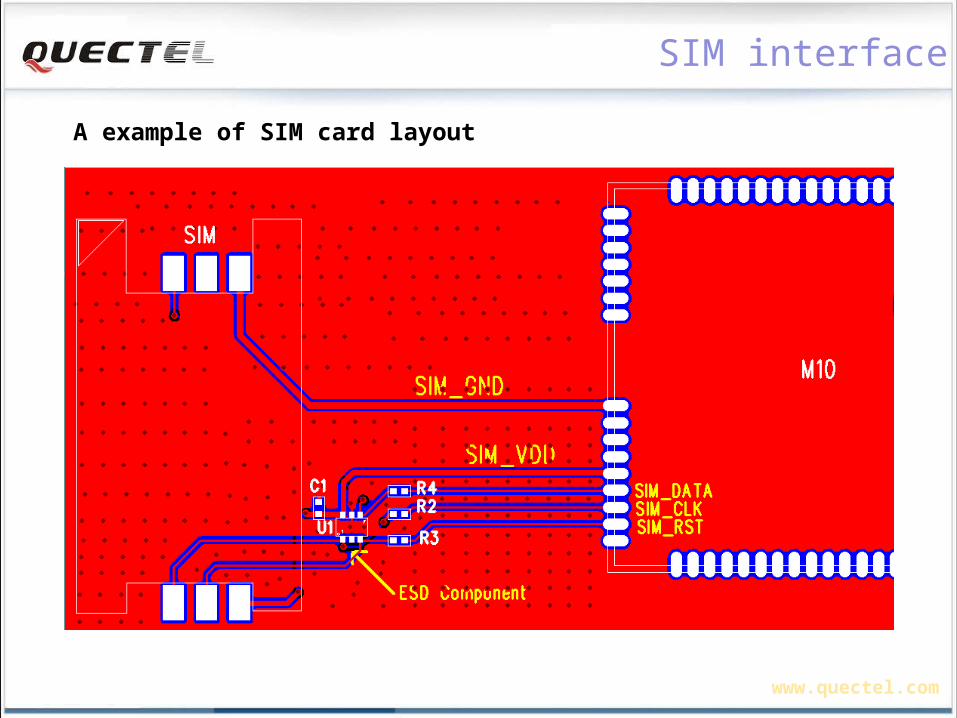
A example of SIM card layout
SIM interface
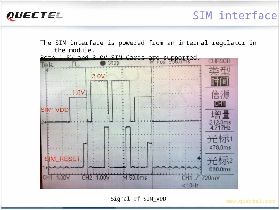
www.quectel.comSignal of SIM_VDD
The SIM interface is powered from an internal regulator in the module. Both 1.8V and 3.0V SIM Cards are supported.
SIM interface
www.quectel.com
Agenda
GSM Modules GSM module family M95 presentation Easy for operating Functions Hardware Software RF designRF design Quectel documents structure
GPS Modules GPS module Portfolio and roadmap Features comparison L70 presentation NMEA protocol
Quectel FAE team Technical Support
www.quectel.com
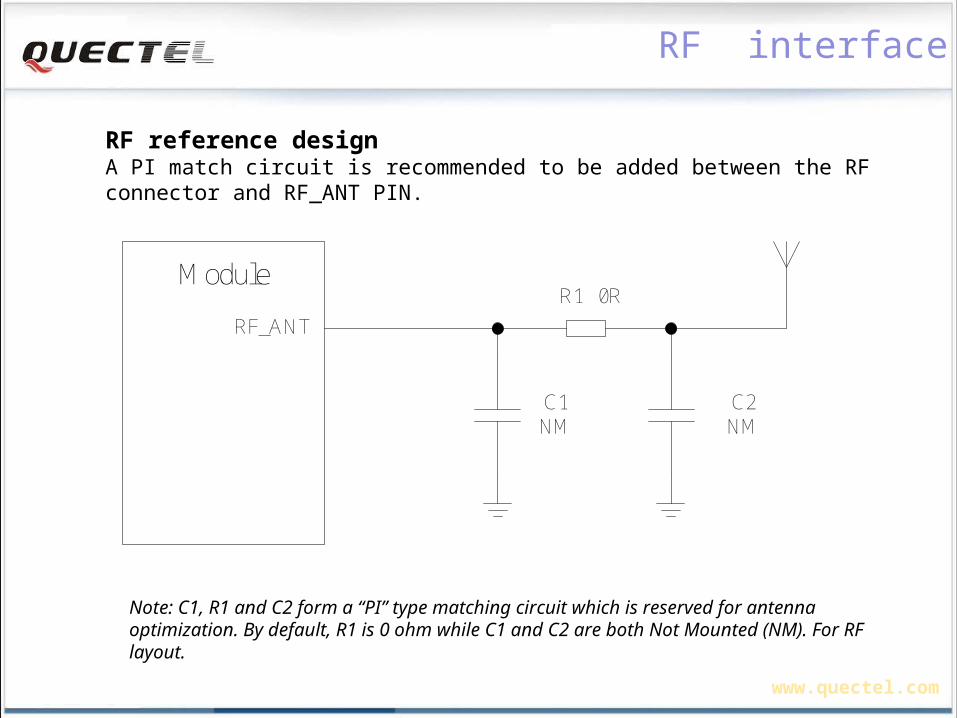
RF interface
Note: C1, R1 and C2 form a “PI” type matching circuit which is reserved for antenna optimization. By default, R1 is 0 ohm while C1 and C2 are both Not Mounted (NM). For RF layout.
RF_ANT
R1 0R
C1NM
C2NM
Module
RF reference design
A PI match circuit is recommended to be added between the RF connector and RF_ANT PIN.
www.quectel.com
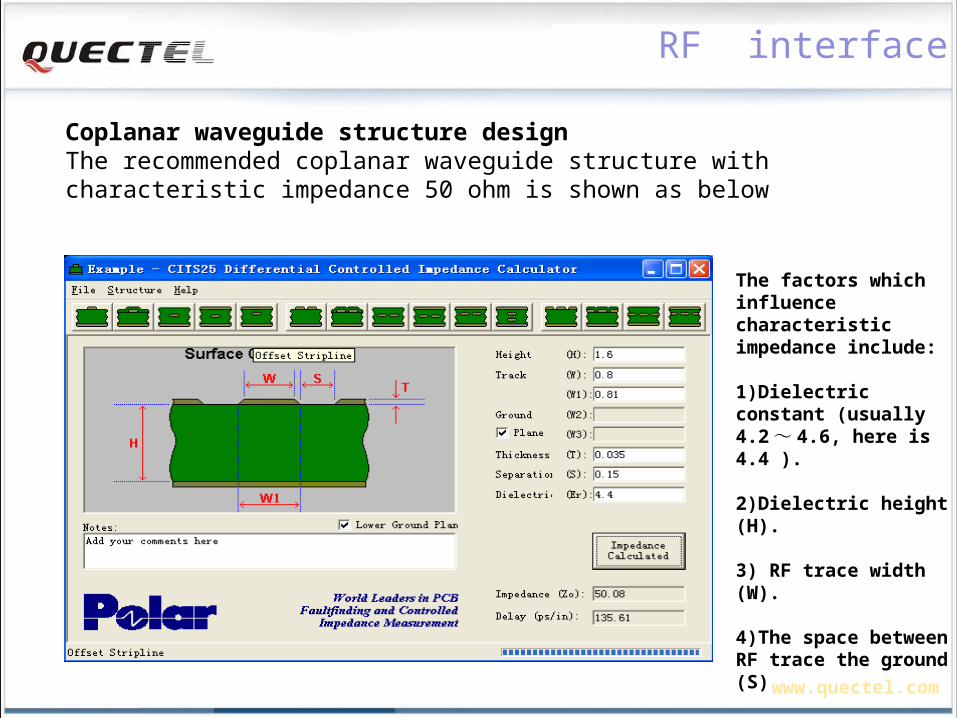
Coplanar waveguide structure designThe recommended coplanar waveguide structure with characteristic impedance 50 ohm is shown as below
The factors which influence characteristic impedance include:
1)Dielectric constant (usually 4.2 ~ 4.6, here is 4.4 ).
2)Dielectric height (H). 3) RF trace width (W).
4)The space between RF trace the ground (S)
5)Copper thickness (T).
RF interface
www.quectel.com
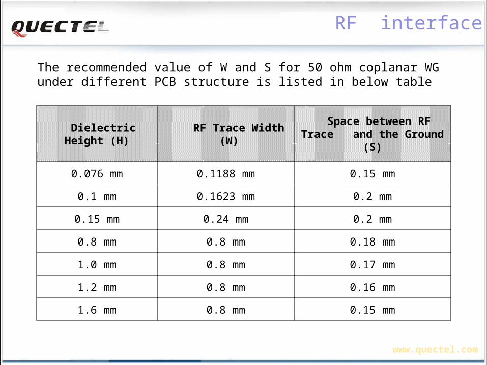
The recommended value of W and S for 50 ohm coplanar WG under different PCB structure is listed in below table
Dielectric Height (H) RF Trace Width
(W) Space between RF Trace
and the Ground (S)
0.076 mm 0.1188 mm 0.15 mm
0.1 mm 0.1623 mm 0.2 mm
0.15 mm 0.24 mm 0.2 mm
0.8 mm 0.8 mm 0.18 mm
1.0 mm 0.8 mm 0.17 mm
1.2 mm 0.8 mm 0.16 mm
1.6 mm 0.8 mm 0.15 mm
RF interface
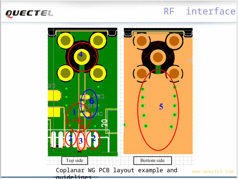
www.quectel.comCoplanar WG PCB layout example and guidelines
6
RF interface
www.quectel.com
1) Control corresponding W and S of 50 ohm coplanar waveguide. Keep in mind that reminding PCB manufacturers of controlling the accuracy of W and S.
2) To achieve good ground performance for RF signal, connect ground pin on either side of RF pin with main ground closely.
3) Keep out pouring copper in the surface layer of RF pin area to reduce parasitic effect. The RF trace line should be as short as possible. It will be better for RF trace line to avoid vertical angle layout.
4) Keep a certain distance between signal pad and ground when using SMA as RF connector. If the signal pad is in SMD type, keep out copper on the corresponding area under signal pad.
5)Ensure the corresponding reference ground of RF trace line is integrated and more ground via is added to help RF reflow. Guarantee the contact area that is in the same layer with RF trace is as large as enough and its corresponding reference ground in the opposite layer is as integrated as possible meanwhile ensure the two layer ground is connected by amount of ground hole.
6) Three components consist of PI type matching circuit shown as Figure 1. Place these components to antenna as closely as possible. If the distance is so short that no component can be placed, the matching circuit also can be removed,
RF interface

www.quectel.com
Agenda
GSM Modules GSM module family M95 presentation Easy for operating Functions Hardware SoftwareSoftware RF design Quectel documents structure
GPS Modules GPS module Portfolio and roadmap Features comparison L70 presentation NMEA protocol
Quectel FAE team Technical Support
www.quectel.com
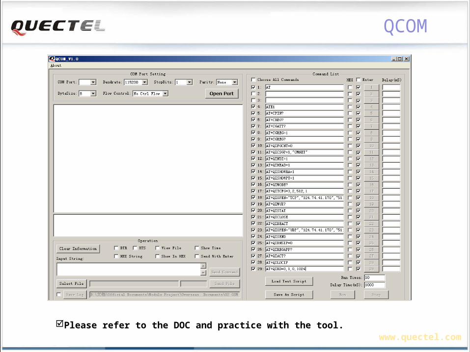
QCOM
Please refer to the DOC and practice with the tool.
www.quectel.com
QServer
Please refer to the DOC and practice with the tool.
www.quectel.com
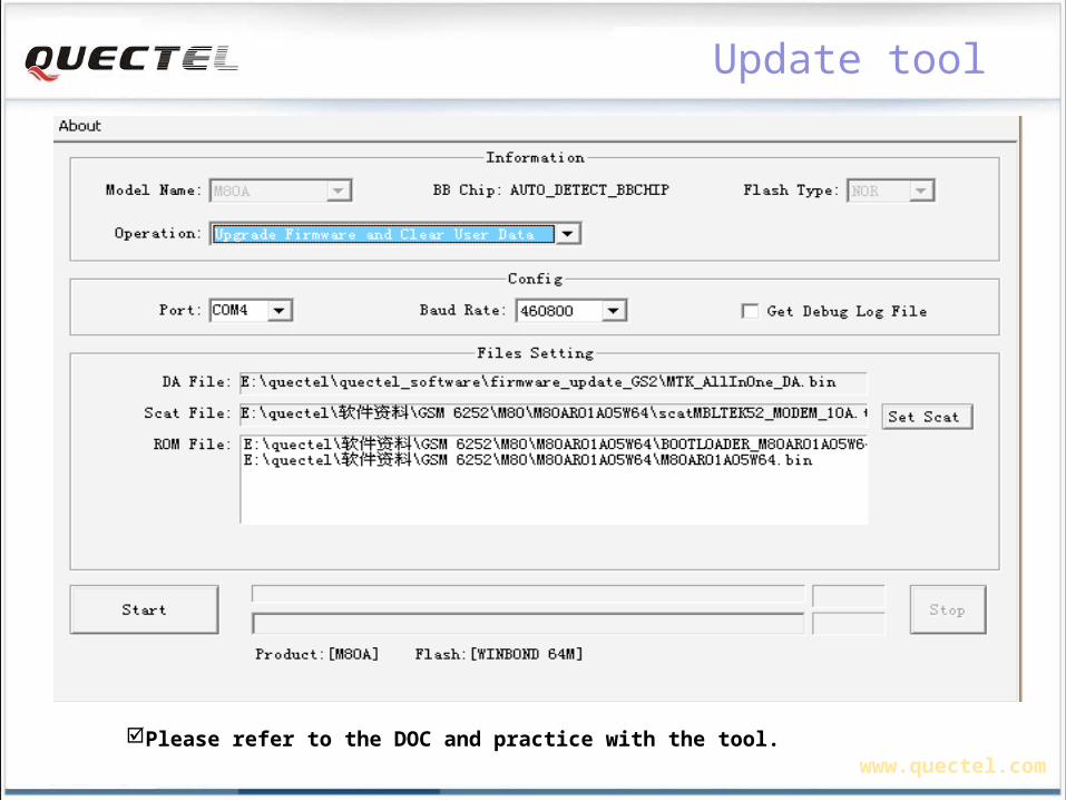
Update tool
Please refer to the DOC and practice with the tool.
www.quectel.com
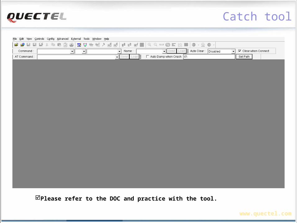
Catch tool
Please refer to the DOC and practice with the tool.
www.quectel.com
Agenda
GSM Modules GSM module family M95 presentation Easy for operating Functions Hardware Software RF design Quectel documents structureQuectel documents structure
GPS Modules GPS module Portfolio and roadmap Features comparison L70 presentation NMEA protocol
Quectel FAE team Technical Support
www.quectel.com
Quectel document structure
CommonDatasheetQuectel GSM Module FamilyApplication Notes GSM_TCPIP_Recommended_ProcessGSM_ATC_AN_V1.00GSM_DTMF_AN_V1.1GSM_FTP_ATCGSM_SMTP_ATC_V1.1GSM_HTTP_ATC_V1.1GSM_SMS_ANGSM_MMS_ATC_V1.1GSM_Jamming_Detection_AN_V1.0GSM_Location_ATC_V1.2RF LAYOUT_AN_V1.0…AN_SpecialFw_Update_Protocol_ANFw_Update_Protocol_AN_V1 3GSM_eCall_AN_V1.1…Development kitQCOM1.1QServer_V1.0Update tool GS1.2Catcher 3.1140.00…
M95DatasheetM10_GSM_Module_SpecificationM95_HD_V1.1M95_ATC_V1.1Development kitM95 Reference DesignM10-EVB_V2.01_SCHM95_Part&Decal…
CertificationM95_CE_CertificateM95_FCC_CertificateM95_IC_CertificateM95_ICASA_CertificateM95_NCC_CertificateM95_RF_Test_ReportM95_EMC_Test_ReportM95_Test_Report…
www.quectel.com
Agenda
GSM Modules GSM module family M95 presentation Easy for operating Functions Hardware Software RF design Quectel documents structure
GPS Modules GPS module Portfolio and roadmapGPS module Portfolio and roadmap Features comparison L70 presentation NMEA protocol
Quectel FAE team Technical Support
www.quectel.com
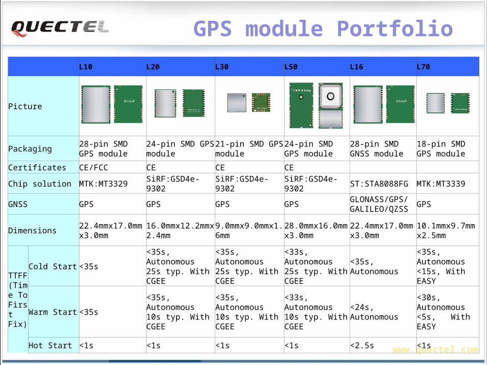
GPS module Portfolio
L10 L20 L30 L50 L16 L70
Picture
Packaging 28-pin SMD GPS module
24-pin SMD GPS module
21-pin SMD GPS module
24-pin SMD GPS module
28-pin SMD GNSS module
18-pin SMD GPS module
Certificates CE/FCC CE CE CE
Chip solution MTK:MT3329 SiRF:GSD4e-9302 SiRF:GSD4e-9302SiRF:GSD4e-9302
ST:STA8088FG MTK:MT3339
GNSS GPS GPS GPS GPSGLONASS/GPS/GALILEO/QZSS
GPS
Dimensions22.4mmx17.0mmx3.0mm
16.0mmx12.2mmx2.4mm
9.0mmx9.0mmx1.6mm
28.0mmx16.0mmx3.0mm
22.4mmx17.0mmx3.0mm
10.1mmx9.7mmx2.5mm
TTFF(Time To First Fix)
Cold Start <35s<35s, Autonomous25s typ. With CGEE
<35s, Autonomous25s typ. With CGEE
<33s, Autonomous25s typ. With CGEE
<35s, Autonomous
<35s, Autonomous<15s, With EASY
Warm Start <35s<35s, Autonomous10s typ. With CGEE
<35s, Autonomous10s typ. With CGEE
<33s, Autonomous10s typ. With CGEE
<24s, Autonomous
<30s, Autonomous<5s, With EASY
Hot Start <1s <1s <1s <1s <2.5s <1s
www.quectel.com
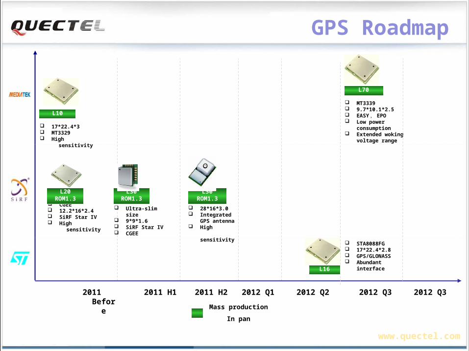
GPS Roadmap
L10
17*22.4*3 MT3329 High sensitivity
2012 Q22011 H2
28*16*3.0 Integrated
GPS antenna
High sensitivity
L50 ROM1.3
Ultra-slim size
9*9*1.6 SiRF Star IV CGEE
L30 ROM1.3 CGEE 12.2*16*2.4 SiRF Star IV High sensitivity
L20 ROM1.3
2012 Q12011 Before 2011 H1
Mass production
In pan
STA8088FG 17*22.4*2.8 GPS/
GLONASS Abundant
interface
2012 Q3
MT3339 9.7*10.1*2.5 EASY , EPO Low power
consumption Extended woking
voltage range
L16
L70
2012 Q3
www.quectel.com
Agenda
GSM Modules GSM module family M95 presentation Easy for operating Functions Hardware Software RF design Quectel documents structure
GPS Modules GPS module Portfolio and roadmap Features comparisonFeatures comparison L70 presentation NMEA protocol
Quectel FAE team Technical Support
www.quectel.com
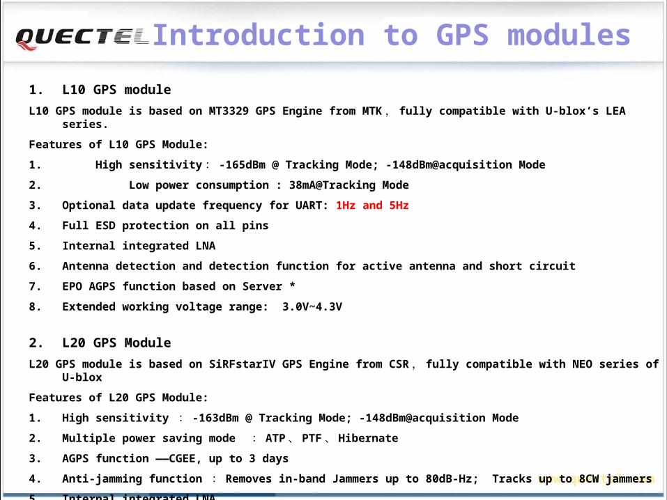
Introduction to GPS modules
1. L10 GPS module
L10 GPS module is based on MT3329 GPS Engine from MTK , fully compatible with U-blox’s LEA series.
Features of L10 GPS Module:
1. High sensitivity : -165dBm @ Tracking Mode; -148dBm@acquisition Mode
2. Low power consumption : 38mA@Tracking Mode
3. Optional data update frequency for UART: 1Hz and 5Hz
4. Full ESD protection on all pins
5. Internal integrated LNA
6. Antenna detection and detection function for active antenna and short circuit
7. EPO AGPS function based on Server *
8. Extended working voltage range: 3.0V~4.3V
2. L20 GPS Module
L20 GPS module is based on SiRFstarIV GPS Engine from CSR , fully compatible with NEO series of U-blox
Features of L20 GPS Module:
1. High sensitivity : -163dBm @ Tracking Mode; -148dBm@acquisition Mode
2. Multiple power saving mode : ATP 、 PTF 、 Hibernate
3. AGPS function ——CGEE, up to 3 days
4. Anti-jamming function : Removes in-band Jammers up to 80dB-Hz; Tracks up to 8CW jammers
5. Internal integrated LNA
www.quectel.com
INTRODUCTION TO GPS MODULES
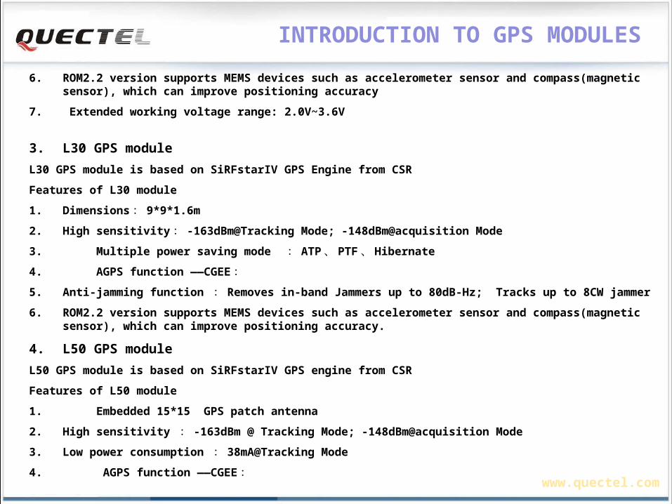
6. ROM2.2 version supports MEMS devices such as accelerometer sensor and compass(magnetic sensor), which can improve positioning accuracy
7. Extended working voltage range: 2.0V~3.6V
3. L30 GPS module
L30 GPS module is based on SiRFstarIV GPS Engine from CSR
Features of L30 module
1. Dimensions : 9*9*1.6m
2. High sensitivity : -163dBm@Tracking Mode; -148dBm@acquisition Mode
3. Multiple power saving mode : ATP 、 PTF 、 Hibernate
4. AGPS function ——CGEE:
5. Anti-jamming function : Removes in-band Jammers up to 80dB-Hz; Tracks up to 8CW jammer
6. ROM2.2 version supports MEMS devices such as accelerometer sensor and compass(magnetic sensor), which can improve positioning accuracy.
4. L50 GPS module
L50 GPS module is based on SiRFstarIV GPS engine from CSR
Features of L50 module
1. Embedded 15*15 GPS patch antenna
2. High sensitivity : -163dBm @ Tracking Mode; -148dBm@acquisition Mode
3. Low power consumption : 38mA@Tracking Mode
4. AGPS function ——CGEE:
www.quectel.com
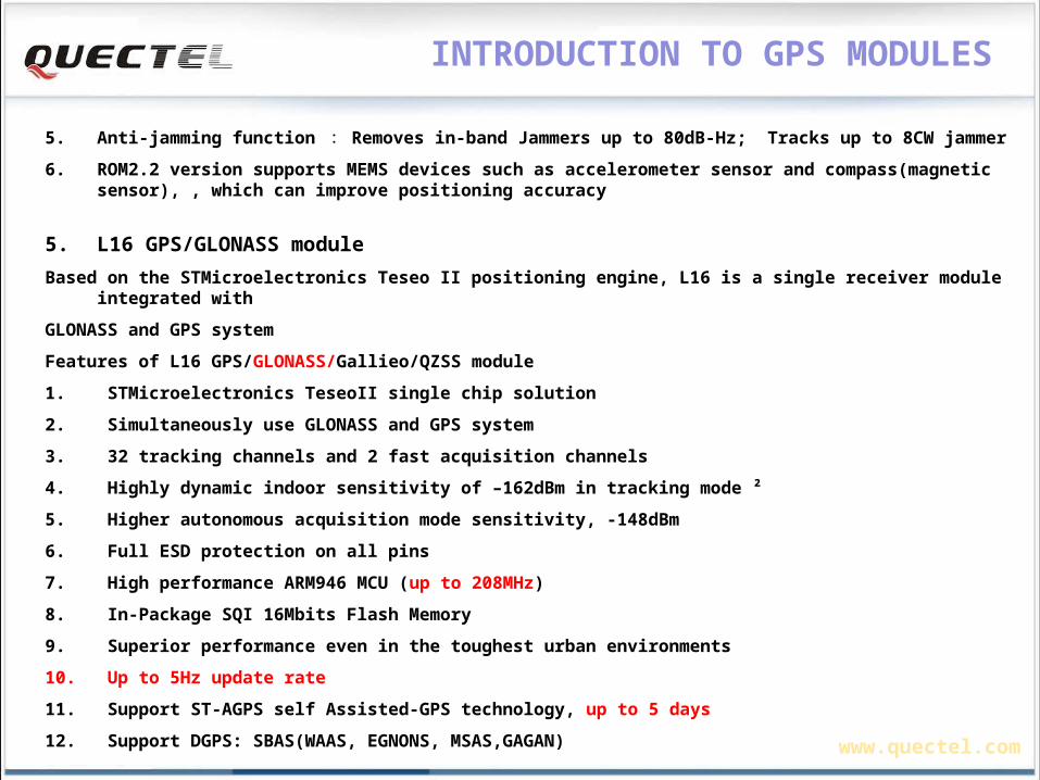
5. Anti-jamming function : Removes in-band Jammers up to 80dB-Hz; Tracks up to 8CW jammer
6. ROM2.2 version supports MEMS devices such as accelerometer sensor and compass(magnetic sensor), , which can improve positioning accuracy
5. L16 GPS/GLONASS module
Based on the STMicroelectronics Teseo II positioning engine, L16 is a single receiver module integrated with
GLONASS and GPS system
Features of L16 GPS/GLONASS/Gallieo/QZSS module
1. STMicroelectronics TeseoII single chip solution
2. Simultaneously use GLONASS and GPS system
3. 32 tracking channels and 2 fast acquisition channels
4. Highly dynamic indoor sensitivity of –162dBm in tracking mode ²
5. Higher autonomous acquisition mode sensitivity, -148dBm
6. Full ESD protection on all pins
7. High performance ARM946 MCU (up to 208MHz)
8. In-Package SQI 16Mbits Flash Memory
9. Superior performance even in the toughest urban environments
10. Up to 5Hz update rate
11. Support ST-AGPS self Assisted-GPS technology, up to 5 days
12. Support DGPS: SBAS(WAAS, EGNONS, MSAS,GAGAN)
INTRODUCTION TO GPS MODULES
www.quectel.com
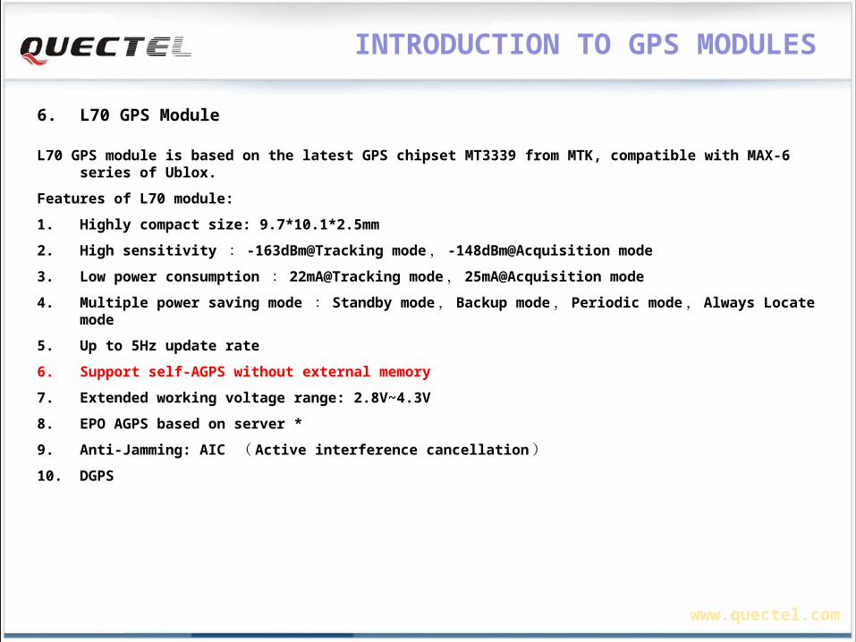
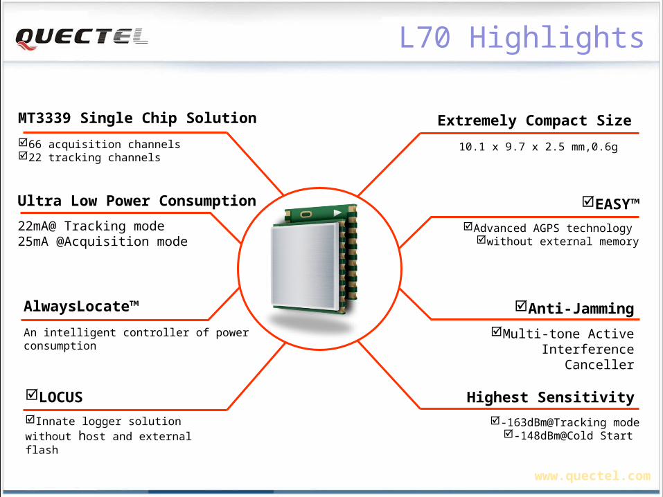
6. L70 GPS Module
L70 GPS module is based on the latest GPS chipset MT3339 from MTK, compatible with MAX-6 series of Ublox.
Features of L70 module:
1. Highly compact size: 9.7*10.1*2.5mm
2. High sensitivity : -163dBm@Tracking mode , -148dBm@Acquisition mode
3. Low power consumption : 22mA@Tracking mode , 25mA@Acquisition mode
4. Multiple power saving mode : Standby mode , Backup mode , Periodic mode , Always Locate mode
5. Up to 5Hz update rate
6. Support self-AGPS without external memory
7. Extended working voltage range: 2.8V~4.3V
8. EPO AGPS based on server *
9. Anti-Jamming: AIC ( Active interference cancellation)
10. DGPS
INTRODUCTION TO GPS MODULES
www.quectel.com
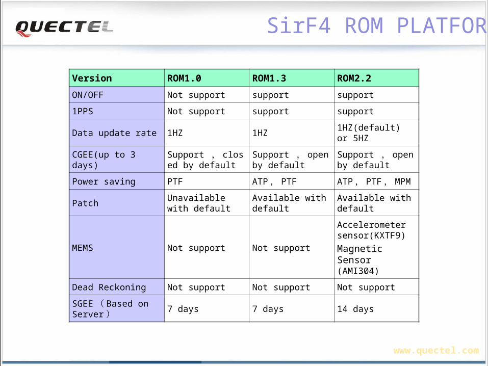
SirF4 ROM PLATFORM
Version ROM1.0 ROM1.3 ROM2.2
ON/OFF Not support support support
1PPS Not support support support
Data update rate 1HZ 1HZ 1HZ(default) or 5HZ
CGEE(up to 3 days)Support , closed by default
Support , open by default
Support , open by default
Power saving PTF ATP , PTFATP , PTF , MPM
PatchUnavailable with default
Available with default
Available with default
MEMS Not support Not support
Accelerometer sensor(KXTF9)
Magnetic Sensor (AMI304)
Dead Reckoning Not support Not support Not support
SGEE ( Based on Server) 7 days 7 days 14 days

www.quectel.com
Agenda
GSM Modules GSM module family M95 presentation Easy for operating Functions Hardware Software RF design Quectel documents structure
GPS Modules GPS module Portfolio and roadmap Features comparison L70 presentationL70 presentation NMEA protocol
Quectel FAE team Technical Support
www.quectel.com
L70 Highlights
EASY™
Advanced AGPS technology without external memory
Highest Sensitivity
-163dBm@Tracking mode-148dBm@Cold Start
AlwaysLocate™
An intelligent controller of power consumption
Extremely Compact Size
10.1 x 9.7 x 2.5 mm,0.6g
MT3339 Single Chip Solution
66 acquisition channels22 tracking channels
Ultra Low Power Consumption
22mA@ Tracking mode 25mA @Acquisition mode
Anti-Jamming
Multi-tone Active Interference Canceller
LOCUS
Innate logger solution without host and external flash

www.quectel.com
Target Applications
Portable Devices
Vehicle Management
Asset Tracking
Security System
Connected PND
GIS Application
Industrial PDA
www.quectel.com
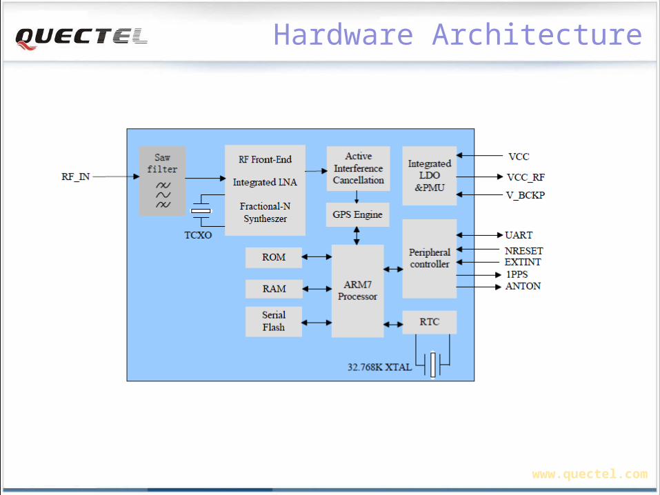
Hardware Architecture
www.quectel.com
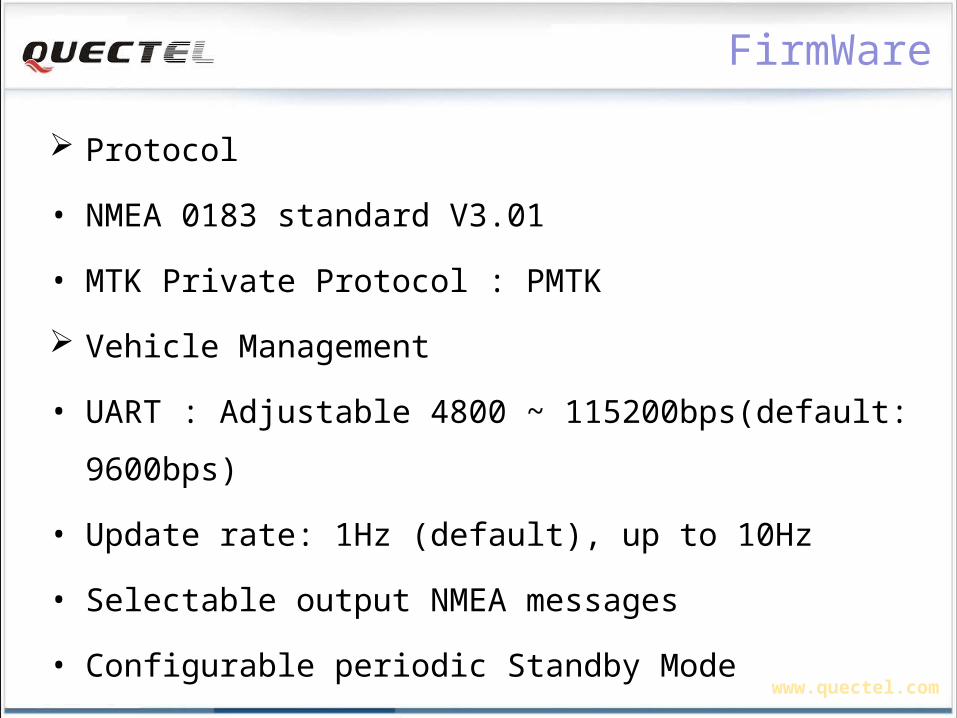
FirmWare
Protocol
• NMEA 0183 standard V3.01
• MTK Private Protocol : PMTK
Vehicle Management
• UART : Adjustable 4800 ~ 115200bps(default: 9600bps)
• Update rate: 1Hz (default), up to 10Hz
• Selectable output NMEA messages
• Configurable periodic Standby Mode
www.quectel.com
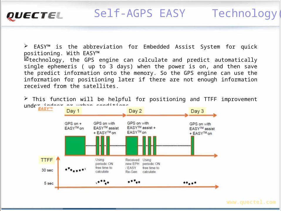
Self-AGPS EASY Technology(1)
EASY™ is the abbreviation for Embedded Assist System for quick positioning. With EASY™ technology, the GPS engine can calculate and predict automatically single ephemeris ( up to 3 days) when the power is on, and then save the predict information onto the memory. So the GPS engine can use the information for positioning later if there are not enough information received from the satellites.
This function will be helpful for positioning and TTFF improvement under indoor or urban conditions.
www.quectel.com
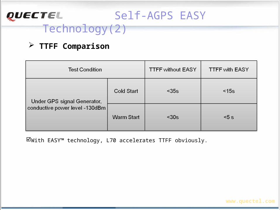
With EASY™ technology, L70 accelerates TTFF obviously.
Self-AGPS EASY Technology(2)
TTFF Comparison
www.quectel.com
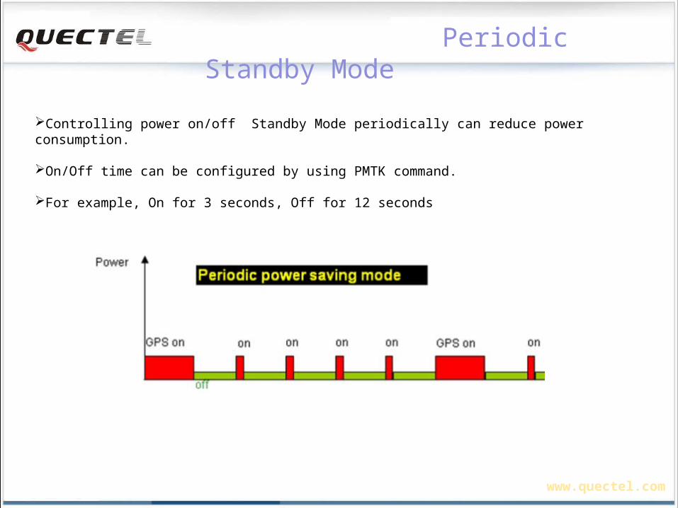
Periodic Standby Mode
Controlling power on/off Standby Mode periodically can reduce power consumption.
On/Off time can be configured by using PMTK command.
For example, On for 3 seconds, Off for 12 seconds

www.quectel.com
AlwaysLocate Technology
AlwaysLocate™ is an intelligent controller of periodic mode.
L70 can adaptively adjust the on/off time to achieve balance between positioning accuracy and power consumption according to the environmental and motion conditions.
www.quectel.com
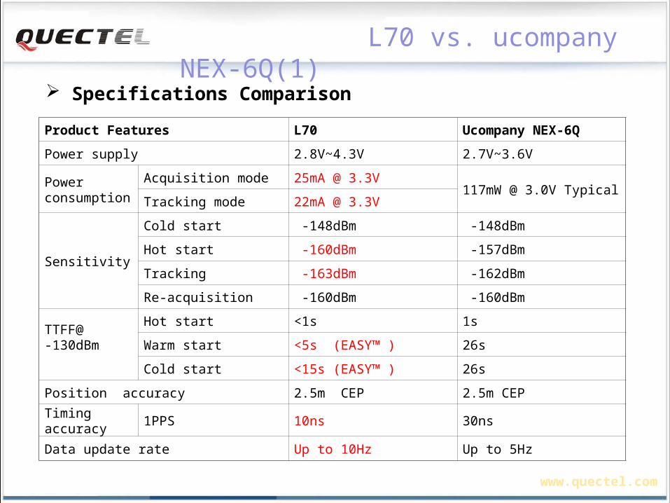
L70 vs. ucompany NEX-6Q(1)
Product Features L70 Ucompany NEX-6Q
Power supply 2.8V~4.3V 2.7V~3.6V
Power consumption
Acquisition mode 25mA @ 3.3V117mW @ 3.0V Typical
Tracking mode 22mA @ 3.3V
Sensitivity
Cold start -148dBm -148dBm
Hot start -160dBm -157dBm
Tracking -163dBm -162dBm
Re-acquisition -160dBm -160dBm
TTFF@-130dBm
Hot start <1s 1s
Warm start <5s (EASY™ ) 26s
Cold start <15s (EASY™ ) 26s
Position accuracy 2.5m CEP 2.5m CEP
Timing accuracy
1PPS 10ns 30ns
Data update rate Up to 10Hz Up to 5Hz
Specifications Comparison
www.quectel.com
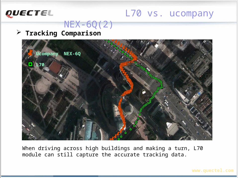
Ucompany NEX-6Q L70
When driving across high buildings and making a turn, L70 module can still capture the accurate tracking data.
L70 vs. ucompany NEX-6Q(2)
Tracking Comparison
www.quectel.com
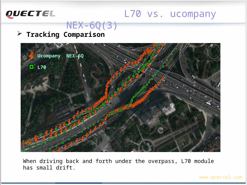
When driving back and forth under the overpass, L70 module has small drift.
L70 vs. ucompany NEX-6Q(3)
Tracking Comparison
Ucompany NEX-6Q L70
www.quectel.com
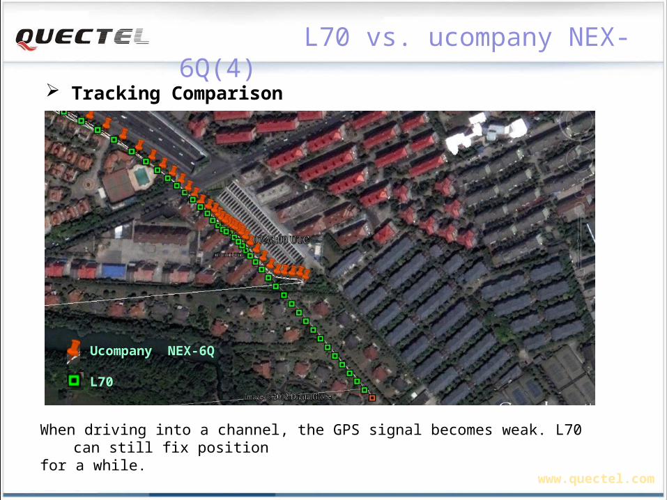
When driving into a channel, the GPS signal becomes weak. L70 can still fix position for a while.
L70 vs. ucompany NEX-6Q(4)
Tracking Comparison
Ucompany NEX-6Q L70
www.quectel.com
Support Package
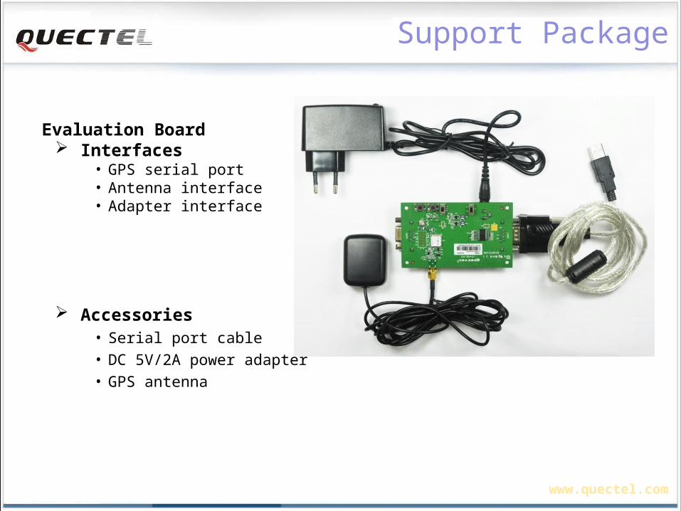
Evaluation Board Interfaces
• GPS serial port• Antenna interface• Adapter interface
Accessories• Serial port cable • DC 5V/2A power adapter• GPS antenna
www.quectel.com
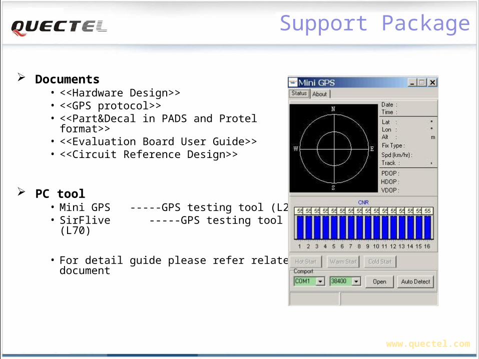
Documents• <<Hardware Design>> • <<GPS protocol>>• <<Part&Decal in PADS and Protel format>>• <<Evaluation Board User Guide>>• <<Circuit Reference Design>>
PC tool• Mini GPS -----GPS testing tool (L20)• SirFlive -----GPS testing tool (L70)
• For detail guide please refer related document
Support Package
www.quectel.com
Agenda
GSM Modules GSM module family M95 presentation Easy for operating Functions Hardware Software RF design Quectel documents structure
GPS Modules GPS module Portfolio and roadmap Features comparison L70 presentation NMEA protocolNMEA protocol
Quectel FAE team Technical Support
www.quectel.com
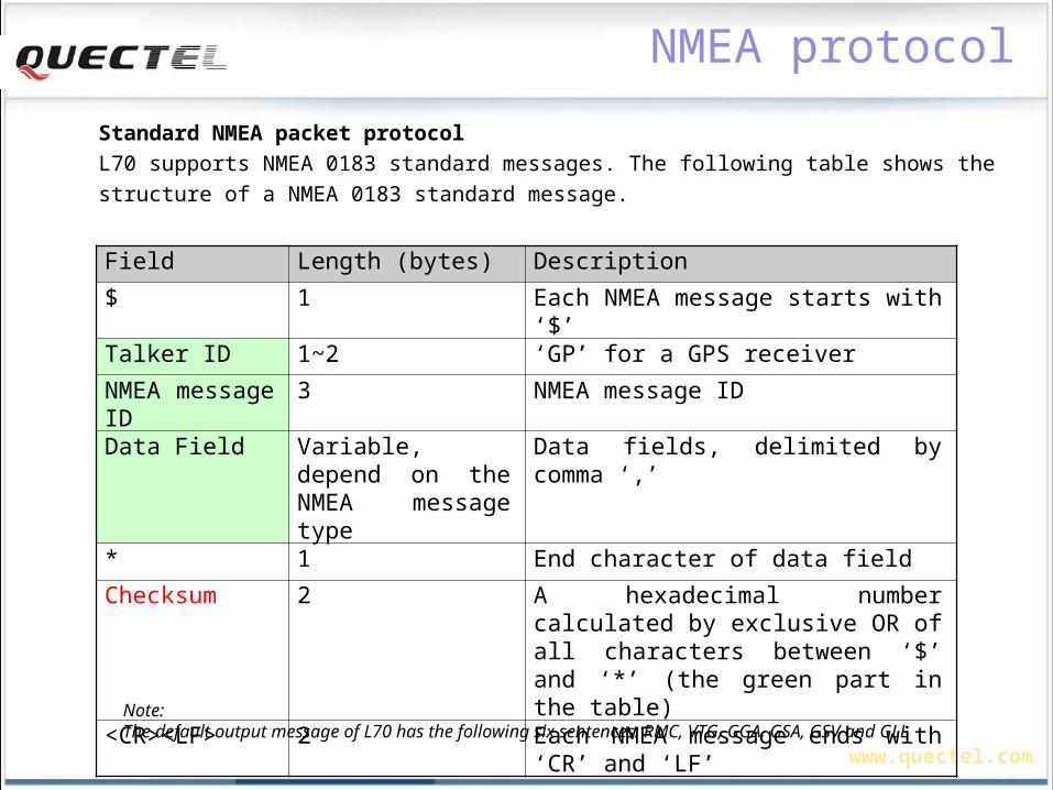
NMEA protocol
Standard NMEA packet protocol
L70 supports NMEA 0183 standard messages. The following table shows the
structure of a NMEA 0183 standard message.
Field Length (bytes) Description
$ 1 Each NMEA message starts with ‘$’
Talker ID 1~2 ‘GP’ for a GPS receiver
NMEA message ID
3 NMEA message ID
Data Field Variable, depend on the NMEA message type
Data fields, delimited by comma ‘,’
* 1 End character of data field
Checksum 2 A hexadecimal number calculated by exclusive OR of all characters between ‘$’ and ‘*’ (the green part in the table)
<CR><LF> 2 Each NMEA message ends with ‘CR’ and ‘LF’
Note:The default output message of L70 has the following six sentences: RMC, VTG, GGA, GSA, GSV and GLL
www.quectel.com
NMEA SENTENCES
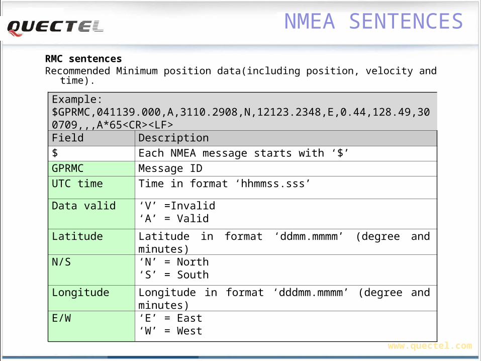
RMC sentencesRecommended Minimum position data(including position, velocity and time).
Example:$GPRMC,041139.000,A,3110.2908,N,12123.2348,E,0.44,128.49,300709,,,A*65<CR><LF>Field Description
$ Each NMEA message starts with ‘$’
GPRMC Message ID
UTC time Time in format ‘hhmmss.sss’
Data valid ‘V’ =Invalid‘A’ = Valid
Latitude Latitude in format ‘ddmm.mmmm’ (degree and minutes)
N/S ‘N’ = North‘S’ = South
Longitude Longitude in format ‘dddmm.mmmm’ (degree and minutes)
E/W ‘E’ = East‘W’ = West
www.quectel.com
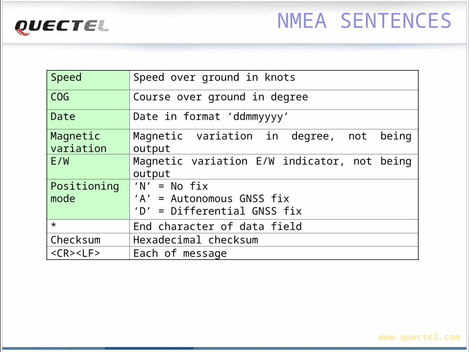
Speed Speed over ground in knots
COG Course over ground in degree
Date Date in format ‘ddmmyyyy’
Magnetic variation
Magnetic variation in degree, not being output
E/W Magnetic variation E/W indicator, not being output
Positioning mode
‘N’ = No fix‘A’ = Autonomous GNSS fix‘D’ = Differential GNSS fix
* End character of data fieldChecksum Hexadecimal checksum<CR><LF> Each of message
NMEA SENTENCES
www.quectel.com
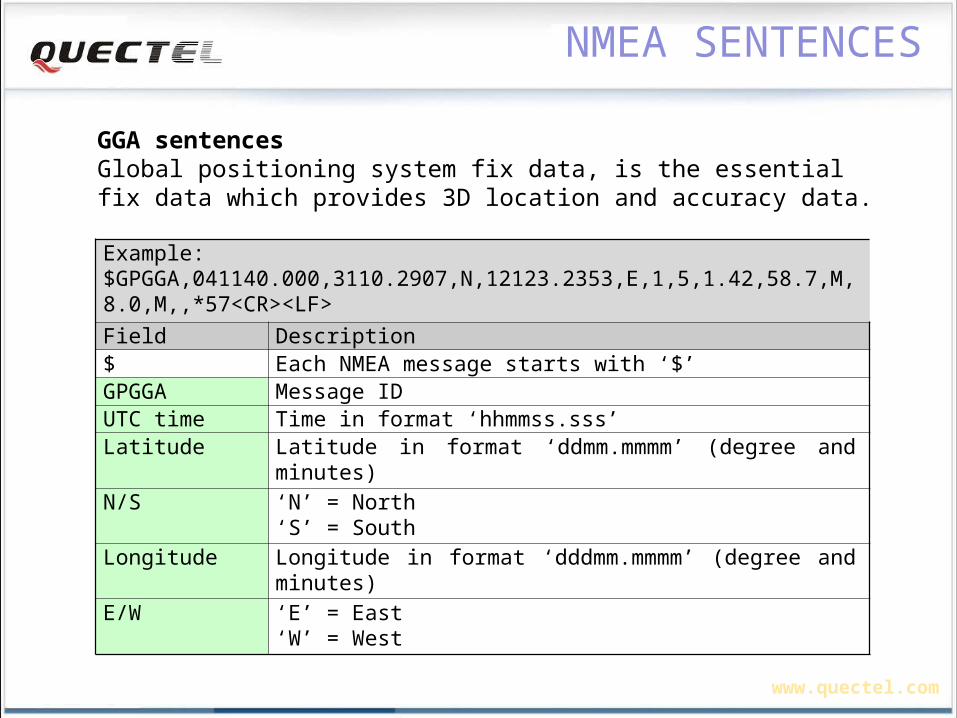
GGA sentencesGlobal positioning system fix data, is the essential fix data which provides 3D location and accuracy data.
Example:$GPGGA,041140.000,3110.2907,N,12123.2353,E,1,5,1.42,58.7,M,8.0,M,,*57<CR><LF>
Field Description$ Each NMEA message starts with ‘$’GPGGA Message IDUTC time Time in format ‘hhmmss.sss’Latitude Latitude in format ‘ddmm.mmmm’ (degree and minutes)
N/S ‘N’ = North‘S’ = South
Longitude Longitude in format ‘dddmm.mmmm’ (degree and minutes)
E/W ‘E’ = East‘W’ = West
NMEA SENTENCES
www.quectel.com
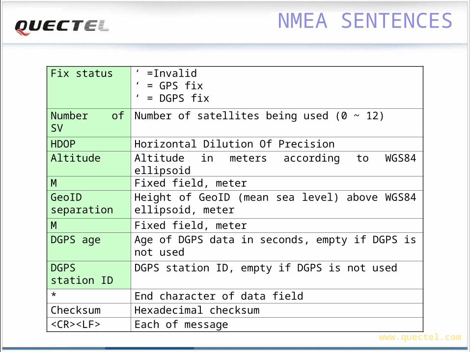
Fix status ‘ =Invalid‘ = GPS fix‘ = DGPS fix
Number of SV Number of satellites being used (0 ~ 12)
HDOP Horizontal Dilution Of PrecisionAltitude Altitude in meters according to WGS84 ellipsoidM Fixed field, meterGeoID separation
Height of GeoID (mean sea level) above WGS84 ellipsoid, meter
M Fixed field, meterDGPS age Age of DGPS data in seconds, empty if DGPS is not used
DGPS station ID
DGPS station ID, empty if DGPS is not used
* End character of data fieldChecksum Hexadecimal checksum<CR><LF> Each of message
NMEA SENTENCES
www.quectel.com
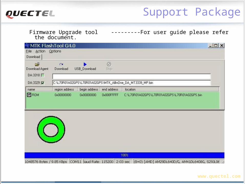
Firmware Upgrade tool ---------For user guide please refer the document.
Support Package
www.quectel.com
Agenda
GSM Modules GSM module family M95 presentation Easy for operating Functions Hardware Software RF design Quectel documents structure
GPS Modules GPS module Portfolio and roadmap Features comparison L70 presentation NMEA protocol
Quectel FAE teamFAE team Technical Support

www.quectel.com
Quectel Teams
Quectel has a diverse and vibrant R&D team, which has rich experience in wireless modules.
Quectel core team members come from world leading cellular module vendors.
Each of them carries 5+ years experience in designing and developing cellular modules. They can assist clients to deliver customized solutions and products in to the market.
Sale and FAE team all over the word
Quectel Teams
www.quectel.com
Agenda
GSM Modules GSM module family M95 presentation Easy for operating Functions Hardware Software RF design Quectel documents structure
GPS Modules GPS module Portfolio and roadmap Features comparison L70 presentation NMEA protocol
Quectel FAE team Technical SupportTechnical Support

www.quectel.com
Technical Support
Complete Technical Support
1. We review customer designs, including schematic, PCB layout and software source code.
2. We also offer to conduct RF tests, HW verifications and give S/W and/or H/W optimization recommendations to our customers.
3. Any problem, just contact us and we will provide the most comprehensive support to our customer with our best.

www.quectel.com
Q&A
The End