training memristors for reliable computing - deep blue - university
TRANSCRIPT

Training Memristors for Reliable Computing
by
Idongesit Effiong Ebong
A dissertation submitted in partial fulfillmentof the requirements for the degree of
Doctor of Philosophy(Electrical Engineering)
in The University of Michigan2013
Doctoral Committee:
Professor Pinaki Mazumder, ChairAssistant Professor Kira BartonAssociate Professor Igor L. MarkovAssistant Professor Zhengya Zhang

c© Idongesit Effiong Ebong 2013
All Rights Reserved

For my family
ii

ACKNOWLEDGEMENTS
This dissertation would not have been successful without the advice, funding,
guidance, and help from my advisor, Prof. Pinaki Mazumder. He taught me valuable
lessons in identifying research areas and ways to position myself in order to succeed.
His encouragement throughout my journey at Michigan is very much appreciated. I
am also immensely grateful for the assistance of my dissertation committee. They
asked very insightful questions that guided me on how to strengthen my work.
I appreciate the level of support I received from the system set up at Michigan and
would like to thank my academic advisor, Prof. Michael Flynn. He was very helpful
when I was crafting my course plans, and also very understanding when advising on
personal issues. I would like to thank Prof. Alexander Ganago, whom I have learned
so much from regarding teaching. In addition, I would like to thank all the professors
whose courses I have had the pleasure of attending. The formal lessons received from
my courses have contributed to my understanding of various subject matters and
enabled the completion of this thesis.
Many thanks to the past and current members of the NDR research group. Manoj
Rajagopalan helped me situate in the group, answering my questions on programming
languages. Dr. Kyungjun Song displayed model work ethic and encouraged me to stay
on a set graduation plan. Yalcin Yilmaz, Jaeyoung Kim, Zhao Xu, and Mahmood
Barangi have become very good friends and have taught me much about life and
work. They have answered questions in regard to their area of expertise and aided
with simulation work in this dissertation and other coauthored papers not part of this
iii

dissertation.
Special thanks to Rackham Graduate School (RGS) and EECS staff, who have
supported me throughout my endeavors. I cannot name them all, but Stephen Reger
has provided much needed help navigating the administrative part of the department.
Joel VanLaven has helped with Cadence and software related issues. Beth Stalnaker
and Karen Liska have provided help relating to GSI assignments, graduation require-
ments, and fellowship materials. RGS provided pivotal financial support for two years
of my studies.
Moving alone to Michigan was a huge life change, so I would like to thank my
SMES-G family for helping me acclimate to the local scene in Ann Arbor. Special
thanks to Michael Logue, for serving as a mentor, listening to my complaints, and
providing encouragement; Prof. Kyla McMullen, for providing feedback on my dis-
sertation; and Dr. Memie Ezike, for providing advice on the future and keeping me
focused.
I have had an incredible support structure and would like to give well deserved
thanks to all my friends. I would like to specifically thank Claudia Arambula for being
my confidante since high school; Chen Huang for professional, as well as, personal
advice since CMU; Dr. Min Kim for getting me into the life-altering habit of running;
Precious Ugwumba for helping me navigate cultural issues; and Rachel Patrick for
incredible homemade meals and laughter.
During my tenure at Michigan, I have been adopted by different families would like
to thank them all for bearing with my quirks. Thank you Mike and Cindy Gillespie for
opening up your home and providing great opportunities to explore and experience
new hobbies I would not attempt on my own. Thanks for the great memories at
Higgins and Chelsea, and for the love you have shown to make Ann Arbor more of
a home to me. Thanks to my church family at Grace Ann Arbor with whom I have
been able to fellowship and discuss the Word. Thanks to Cloyd and Betty Peters,
iv

who have shown that having community roots and dedication to uplifting the youth
are important aspects to success.
I pulled Jessica Gillespie alongside me as I treaded through my Michigan journey.
I would like to thank her for enduring part of this dissertation process with me. She
improved my emotional health and provided consistent challenges that helped me
avoid being a hermit, cloistered away in the office.
I would like to thank my family for being there for me. Thanks to my parents,
Effiong and Affiong Ebong, for their support and encouragement throughout life.
I thank my uncle and aunty, Prof. Abasifreke Ebong and Uduak Ebong, for also
serving parental roles and providing much needed guidance through these years. My
siblings, Iniubong Ebong, Dr. Ekaette Ebong, and Emem Ebong, have played pivotal
roles in molding me to the person I am today, and I thank them all for their love,
encouragement, and support. My sisters, Imabasi, Eti, and Eka Ebong, thank you
for giving me reasons to continue my studies. And thanks to all the aunties, uncles,
and cousins all over the world who have supported my endeavors.
Lastly, I would like to thank God for the wonderful blessings and answered prayers.
He provided me with families and friends away from home so I would not be alone.
He made sure to put influences in my life, both academically and emotionally, to keep
me going. This journey would not have been possible without Him.
v

TABLE OF CONTENTS
DEDICATION . . . . . . . . . . . . . . . . . . . . . . . . . . . . . . . . . . ii
ACKNOWLEDGEMENTS . . . . . . . . . . . . . . . . . . . . . . . . . . iii
LIST OF FIGURES . . . . . . . . . . . . . . . . . . . . . . . . . . . . . . . viii
LIST OF TABLES . . . . . . . . . . . . . . . . . . . . . . . . . . . . . . . . xi
ABSTRACT . . . . . . . . . . . . . . . . . . . . . . . . . . . . . . . . . . . xii
CHAPTER
I. Introduction . . . . . . . . . . . . . . . . . . . . . . . . . . . . . . 1
1.1 Motivation . . . . . . . . . . . . . . . . . . . . . . . . . . . . 11.2 Memristor Applications . . . . . . . . . . . . . . . . . . . . . 31.3 Thesis Organization . . . . . . . . . . . . . . . . . . . . . . . 7
II. Memristor Background . . . . . . . . . . . . . . . . . . . . . . . . 10
2.1 Introduction . . . . . . . . . . . . . . . . . . . . . . . . . . . 102.2 Chua’s modeling of memristors and memristive systems . . . 102.3 Experimental realizations of memristors . . . . . . . . . . . . 142.4 Memristor modeling in this thesis . . . . . . . . . . . . . . . . 172.5 Chapter Conclusion . . . . . . . . . . . . . . . . . . . . . . . 22
III. Neuromorphic Building Blocks with Memristors . . . . . . . . 24
3.1 Introduction . . . . . . . . . . . . . . . . . . . . . . . . . . . 243.2 Implementing Neuromorphic Functions with Memristors . . . 263.3 CMOS-Memristor Neuromorphic Chips . . . . . . . . . . . . 343.4 Chapter Summary . . . . . . . . . . . . . . . . . . . . . . . . 48
IV. Memristor Digital Memory . . . . . . . . . . . . . . . . . . . . . 50
vi

4.1 Introduction . . . . . . . . . . . . . . . . . . . . . . . . . . . 504.2 Adaptive Reading and Writing in Memristor Memory . . . . 524.3 Simulation Results . . . . . . . . . . . . . . . . . . . . . . . . 574.4 Adaptive Methods Results and Discussion . . . . . . . . . . . 694.5 Chapter Summary . . . . . . . . . . . . . . . . . . . . . . . . 73
V. Value Iteration with Memristors . . . . . . . . . . . . . . . . . . 75
5.1 Introduction . . . . . . . . . . . . . . . . . . . . . . . . . . . 755.2 Q-Learning and Memristor Modeling . . . . . . . . . . . . . . 775.3 Maze Search Application . . . . . . . . . . . . . . . . . . . . 805.4 Results and Discussion . . . . . . . . . . . . . . . . . . . . . . 855.5 Chapter Conclusion . . . . . . . . . . . . . . . . . . . . . . . 88
VI. Closing Remarks and Future Work . . . . . . . . . . . . . . . . 89
6.1 Chapter Conclusions . . . . . . . . . . . . . . . . . . . . . . . 896.2 Future Work . . . . . . . . . . . . . . . . . . . . . . . . . . . 91
APPENDIX . . . . . . . . . . . . . . . . . . . . . . . . . . . . . . . . . . . . 93
BIBLIOGRAPHY . . . . . . . . . . . . . . . . . . . . . . . . . . . . . . . . 105
vii

LIST OF FIGURES
Figure
2.1 Relationship between all four circuit variables and their constitutivecircuit elements . . . . . . . . . . . . . . . . . . . . . . . . . . . . . 11
2.2 HP memristor device showing appropriate layers and identifying theohmic and non-ohmic contacts . . . . . . . . . . . . . . . . . . . . . 15
2.3 Normalized ∆C vs. Vab showing proportional magnitude of conduc-tance change as a function of applied bias . . . . . . . . . . . . . . . 21
2.4 MT vs. φ showing two regions of operation for the memristor . . . . 21
3.1 Recurrent network architecture showing an example of how Winner-Take-All, lateral inhibition, or inhibition of return can be connectedusing crossbars . . . . . . . . . . . . . . . . . . . . . . . . . . . . . 28
3.2 STDP curves showing relationship between synaptic weight changeand the difference in spike times between the pre-neuron and thepost-neuron . . . . . . . . . . . . . . . . . . . . . . . . . . . . . . . 31
3.3 Neural network implemented in Verilog in order to determine noisyperformance of STDP in comparison to digital logic . . . . . . . . . 32
3.4 Neuron layer connectivity showing position detector architecture (cir-cles are neurons and triangles are synapses) . . . . . . . . . . . . . . 35
3.5 STDP Synapse Circuit Diagram implemented in CMOS . . . . . . . 37
3.6 Pre-neuron and post-neuron spiking diagram showing three pulsesabove the memristor’s threshold . . . . . . . . . . . . . . . . . . . . 38
3.7 Neuron circuit that can provide spiking pattern for STDP realizationwith memristors . . . . . . . . . . . . . . . . . . . . . . . . . . . . . 38
viii

3.8 FSM showing control signal generation . . . . . . . . . . . . . . . . 39
3.9 Neuromorphic architecture for the multi-function digital gate showingneurons and synapses . . . . . . . . . . . . . . . . . . . . . . . . . . 43
3.10 Training mode using prescribed XOR training scheme . . . . . . . . 45
3.11 XOR simulation results . . . . . . . . . . . . . . . . . . . . . . . . . 46
3.12 (Left) Edge detection simulation results for input pattern “011110”produces output pattern “010010”. (Right) Edge detection simu-lation results for input pattern “100110” produces output pattern“100110” . . . . . . . . . . . . . . . . . . . . . . . . . . . . . . . . . 49
4.1 Memory system top-level block diagram . . . . . . . . . . . . . . . . 51
4.2 (a) Read flow diagram. (b)Write/erase flow diagram . . . . . . . . . 54
4.3 Memory cell read operation showing the different phases of read:equalize, charge v1, charge v2, no op, and sense enable . . . . . . . 56
4.4 Read sense circuitry: (a) Sampling circuit that converts current throughRmem to voltage (b) Sense amplifier that determines HIGH or LOWresistive state . . . . . . . . . . . . . . . . . . . . . . . . . . . . . . 56
4.5 Simulation Results Writing to an RRAM cell (a) Low/High Resis-tance Signals (b) Memristance High Resistance to Low Resistanceswitch . . . . . . . . . . . . . . . . . . . . . . . . . . . . . . . . . . 57
4.6 Simulation Results Erasing an RRAM Cell (a) Low/High ResistanceSignals (b) Memristance Low Resistance to High Resistance switch . 58
4.7 Writing in the BRS Case showing that resistance background hasminimal effect on the number of read cycles required for a write . . 59
4.8 Erasing in the BRS Case showing that resistance background hasminimal effect on the number of read cycles required for an erase . . 60
4.9 Percent change in unselected devices during an erase for differentminimum resistances . . . . . . . . . . . . . . . . . . . . . . . . . . 61
4.10 Writing to memristor devices with the same high resistive state butvarying low resistive states (coarse spread) . . . . . . . . . . . . . . 63
ix

4.11 Writing under different diode leakage conditions . . . . . . . . . . . 64
4.12 Memristor changes under the different leakage conditions showingthat the Read/Write failure in Figure 4.11 is not because of charac-teristic deviation but because of sensing methodology drawback . . 65
4.13 Equivalent circuit schematic showing the components considered inpower analysis (note that series diode RD << M1) . . . . . . . . . . 66
4.14 Writing to memristor devices with the same high resistive state butvarying low resistive states . . . . . . . . . . . . . . . . . . . . . . . 70
5.1 Maze example showing starting position (green square) and endingposition (red square) . . . . . . . . . . . . . . . . . . . . . . . . . . 81
5.2 (a) Top Level system showing information flow (b) Network schematicshowing analog and digital components . . . . . . . . . . . . . . . . 82
5.3 (a) Activation of neurons (b) Equivalent circuit of activated devices 85
5.4 (a) Number of terms vs. the percent error (b) Effect of vthresh on thecharging time to spike (c) Number of steps before convergence usingthe baseline value function (d) Number of steps before convergenceusing memristors . . . . . . . . . . . . . . . . . . . . . . . . . . . . 86
5.5 (a) Optimal path using the baseline value function (b) Near optimalpath using the memristor crossbar (suboptimal moves circled) . . . 87
A.1 BISR example circuitry for a 4x4 fault pattern . . . . . . . . . . . . 96
A.2 Example of programming a BISR memory pattern . . . . . . . . . . 96
A.3 (a) Erasing the fault pattern from the BISR array (b) Programminga specific fault pattern to the BISR array . . . . . . . . . . . . . . . 99
A.4 Fault pattern and transient simulation results showing the selectedneuron coverage scheme for the fault pattern shown . . . . . . . . . 102
A.5 Fault pattern and transient simulation results showing the selectedneuron coverage solution for the fault pattern shown . . . . . . . . . 103
x

LIST OF TABLES
Table
3.1 Verilog STDP Output Neuron Results for an Object Placed at Dif-ferent Locations on the 1D Position Detection Line . . . . . . . . . 34
3.2 Design summary for both proposed WTA CMOS and MMOST 5X5Position Detector Arrays . . . . . . . . . . . . . . . . . . . . . . . . 39
4.1 Power and Energy results . . . . . . . . . . . . . . . . . . . . . . . . 70
xi

ABSTRACT
Training Memristors for Reliable Computing
by
Idongesit Effiong Ebong
Chair: Pinaki Mazumder
The computation goals of the digital computing world have been segmented into
different factions. The goals are no longer rooted in a purely speed/performance
standpoint as added requirements point to much needed interest in power awareness.
This need for technological advancement has pushed researchers into a CMOS+X
field, whereby CMOS transistors are utilized with emerging device technology in a
hybrid space to combine the best of both worlds. This dissertation focuses on a
CMOS+Memristor approach to computation since memristors have been proposed
for a large application space from digital memory and digital logic to neuromorphic
and self-assembling circuits.
With the growth in application space of memristors comes the need to bridge the
gap between complex memristor-based system proposals and reliably computing with
memristors in the face of the technological difficulties with which it is associated. In
order to account for these issues, research has to be pushed on two fronts. The first
is from the processing viewpoint, in order to have a better control on the fabrication
process and increase device yield. The second is from a circuits and architecture
technique and how to tolerate the effects of a non-ideal process. This thesis takes the
xii
approach of the latter in order to provide a pathway to realizing the many applications
suggested for the memristor.
Specifically, three application spaces are investigated. The first is a neuromorphic
approach, whereby spike-timing-dependent-plasticity (STDP) can be combined with
memristors in order to withstand noise in circuits. We show that the analog approach
to STDP implementation with memristors is superior to a digital-only approach. The
second application is in memory; specifically, we show a procedure to program and
erase a memristor memory. The procedure is proven to have an adaptive scheme that
stems from device properties and makes accessing the memristor memory more reli-
able. The third approach is an attempt to bridge higher level learning to a memristor
crossbar, therefore paving the way to realizing self-configurable circuits. The ap-
proach, or training methodology, is compared to Q-Learning in order to re-emphasize
that reliably using memristors may require not knowing the precise resistance of each
device, but instead working with relative magnitudes of one device to another. This
dissertation argues for the adoption of training methods for memristors that exhibit
relative magnitudes in order to overcome reliability issues and realize applications
proposed for the memristor.
xiii
CHAPTER I
Introduction
1.1 Motivation
The computation goals of the digital computing world have been segmented into
different factions. The goals are no longer rooted in a purely speed/performance
standpoint but added requirements point to much needed interest in power aware-
ness [107]. In addition to the added power efficiency metrics, the transistor scaling
requirements imposed upon by Moore’s Law continue to drive the digital computing
world to fit more options, processes, and systems on a smaller and smaller area. How-
ever, CMOS technology will eventually encounter physical and manufacturing limita-
tions, thereby ending the era of transistor scaling. In order to sustain the exponential
scaling of the integrated circuits espoused by Moore’s Law, several non-CMOS tech-
nologies have been investigated. These technologies include, but are not limited to,
Ferroelectric RAM [59], Spin-transfer torque (STT-RAM [16]), Phase change memory
(PCRAM [110][78]) and other resistive RAM (RRAM) devices [111], molecular and
macromolecular memory [75], and nanomechanical memory [64]. ITRS recognizes the
feasibility of these devices with respect to scaling and provides a table comparison
[100].
The comparison in ITRS cites these emerging technologies as memory replace-
ments in current CMOS technology. Memory is targeted because as integration den-
1

sity grows, power consumption due to leakage in memory also increases (which is bad
news because chip sizes in effect are dominated by on-chip memory). The emerging
technologies are in effect viewed as technologies that will revolutionize memory and
therefore reach the targeted goals of higher device integration as well as low power
performance. Memories employing the emerging technologies are expected to have
significant leakage power reduction because almost all proposed technologies have a
nonvolatile property. When not in use, the power to the memory can be shut off
thereby eliminating wasted power due to leakage, and the devices will “remember”
their previous states when power is restored for computation.
Under the umbrella of emerging technologies, this thesis deals specifically with the
RRAM and memristor devices. These devices are chosen because of their ability to
skirt both digital [29] and analog [41] processing domains. The memristor device is
not just viewed as a memory element; they can perform simple computation, therefore
replacing the need for multiple transistors on chip. In addition, the RRAM technology
with memristors provides a pathway to scale devices down to 5 nm. With promising
prospects in continued scaling and higher level processing, memristors have been
proposed for different applications.
The call for different applications also comes with a paradigm shift in the best
way to realize digital and analog systems. A design approach catering to the device
properties signals that the best way to efficiently use the memristor may actually
be to depart from conventional digital processing methods. Sequential processing
through the classical architecture of conventional digital computers has produced
very complex, power hungry machines. Only recently has the industry been pushed to
consider parallel processing for algorithm implementation [3]. By successfully meeting
speed and performance milestones, the emulation of a mouse’s brain is possible using
the digital computer, but the energy and power requirement has grown exponentially
as the computer’s complexity has increased [3]. Biological architectures, on the other
2

hand, are configured very differently and possess a power efficiency that far exceeds
that of the digital computer.
Biological architectures are dependent on complex electrochemical synapses and
parallel computing. Different pathways, i.e., visual, auditory, tactile, olfactory, and
gustation, are all used to make conclusions about perceived information. In accor-
dance, motor control is used to react to the information acquired by these different
pathways or sensors. There not only exists the ability to decipher information, but
also the capacity to correct or react to a sensation. Realization and demonstration of
a bio-inspired system with comparable power budgets to the biological world is the
Holy Grail for the memristor-laden technology. In order to achieve the many proposed
applications, better ways of training the memristor to obtain reliable, reproducible
behavior is necessary. This thesis provides three methods of training the memristor.
The first training method is applicable to neuromorphic circuitry, the second training
method is applicable to a digital memory system, and the final training method is
inspired by reinforcement learning and may pave a way for self-organizing circuits.
The next section provides an overview for a better understanding of the application
space of memristors.
1.2 Memristor Applications
The information in this section draws mostly from [53]. Memristor applications
are broadly categorized into two clusters whereby memristors are used either as dis-
crete devices or in an array configuration. The discrete device advocates tend to use
memristors as single elements in order to take advantage of the nonlinear properties
each memristor exhibits. The array configuration, on the other hand, places an em-
phasis on using memristors in a nano crossbar, thereby primarily reaping benefits of
the crossbar’s high density structure, with memristor’s nonlinear properties viewed as
a secondary benefit. In the crossbar array configuration, proposed memristors appli-
3

cations include: neuromorphic networks, field programmable analog arrays (FPAA),
content addressable memory (CAM), resistive random access memory (RRAM), and
logic circuits. For the discrete component category, the proposed applications are:
chaos circuits, Schmitt trigger, variable gain amplifier, difference comparator, cellular
neural networks (CNNs), oscillators, logic operations, digital gates, and reconfigurable
logic circuits.
The broadly defined categories (discrete vs. crossbar) with their respective appli-
cations are by no means definite in nature, for some applications can skirt both cate-
gories depending on proposed usage. For example, spike-timing-dependent-plasticity
(STDP) [89] and associative memory [70] are proposed as discrete device applica-
tions, but the spirit of both works is an array application. This is due to the fact
that, although not explicitly mentioned, the transformative impact of utilizing the
memristors discretely for the selected applications may not be much compared to the
state of the art. This reasoning is behind why memory applications and neuromor-
phic applications are classified as crossbar applications; even though, the papers cited
may only focus on a small part of the learning or programming mechanism rather
than an entire system. The applications that will be expounded upon in detail are:
non-volatile memory, neuromorphic circuits, reconfigurable logic, and logic gates.
Non-volatile memory (NVM) is the most mature of all the applications, not only
because of the aforementioned problems of high leakage power consumption in CMOS
chips and scaling limits predicted for memory, but also data centric processing will
fall victim to the memory wall problem [13]. Before proposing memristor realizations
to tackle this problem, PCRAM has been investigated with several prototypes suc-
cessively fabricated in the 90 nm node [4] and 45 nm node [86]. Currently various
memristor forms are being investigated in tandem with PCRAM, including metal
oxide based devices [66] and programmable metalization cells (PMC) based on solid
state electrolytes [46]. Various problems arise with memristor memories and Chap-
4

ter IV deals in detail with an adaptive scheme designed to ameliorate some of the
issues. In addition to improving memory yield, the repair technique in Appendix A
may also be employed. Programming, erasing, and yield are not the only challenges
associated with memory. Flash memory (today’s solid state NVM leader) has the
capability of multibit cells, therefore, in order to match and exceed storage capacity
of flash, memristors should also employ multibit cells. Issues associated with reliable
multibit cell memristors are covered in [51]. A good reference for RRAM with metal
oxides is [2]. A CAM memory structure with memristors is discussed in [30]. A
CAM structure is similar to digital RAM; the difference between both lies in usage
and function. CAMs receive data as inputs, perform a whole memory search, and
then return the address that stores the values that match the input data. RAMs, on
the other hand, receive an address and will provide the data stored at the specified
address.
Digital memory applications lead the discussion to digital logic blocks using mem-
ristors. The experimental, non-volatile synchronous flip flop in [81] shows resiliency
to power losses and boasts an error rate of 0.1% during 1000 power loss events. Along
the lines of digital logic blocks, logic gates [76][12] have been realized with memristors
even though their speed does not match a purely CMOS design [113]. An extension of
gate and memory design is the use of memristors in FPGA design [103][21] and field
programmable nanowire interconnect (FPNI) design [90]. Since memristors can take
on digital states, their use as switches for reconfigurable digital logic is the appeal
in the FPGA and FPNI designs. Logic gate speeds, in essense, would not necessar-
ily be adversely affected by memristor programming speeds, since after configuration
into the logic function specified by the FPGA software, the logic circuits are only
used to evaluate logic functions and further programming will be unnecessary. Logic
gates using implication logic as well as threshold logic have also been investigated
since standard Boolean logic may not be the best utilization of the memristor devices
5

[47][8].
Analog circuits also strive to use memristors to enhance functionality. Analog
circuits usually consume a larger area compared to their digital counterparts, so by
utilizing nanodevices such as memristors, analog circuits may be made more com-
pact. Several applications have been mentioned in literature for analog circuits, and
most use the memristor as a variable resistor thereby allowing for staple items like pro-
grammable amplifiers [68][87]. Memristors have also been proposed for cellular neural
networks (CNN) [39],[48], recurrent neural networks [112], programmable threshold
comparators, Schmitt triggers, difference amplifiers [68], ultra wide band receivers
[108], adaptive filters [56], and oscillators[95]. Chaos circuits are also an interesting
blend for analog applications of memristors because of large benefits that can be
garnered in areas such as secure communication and seizure detection. Second order
effects of a memristor can lead to chaotic behavior when connected to a power source
[25]. Another way to realize chaos with memristors is to replace the Chua diode with
a memristor [38],[62],[6]. An example of using chaos and memristors in an image
encryption application is provided in [49].
There have been multiple displays of using memristors in biomimetic or neuro-
morphic circuits and some of the options are discussed in Chapter III. In the neu-
romorphic circuit approach, observable biological behavior or processing is aimed to
be replicated. Processing elements (or “neuron circuits”) are built with standard
CMOS while the adaptive synapses are achieved using the memristor crossbar. In lit-
erature, various groups have demonstrated through simulation how to achieve STDP
with memristors [89],[27],[84]. We have shown through experimental design with off-
the-shelf components and fabricated memristors that the nanodevices are capable of
mimicking biological synapses and implementing STDP [41]. The conductance of the
memristor can be incrementally adjusted by precisely controlling the electric bias ap-
plied to the pre-synaptic and post-synaptic CMOS neurons. STDP has been verified
6

not just with the a-Si memristor but with a Cu2O device[18]. Future development
of CMOS/memristive systems must be explored further in order to create more bi-
ologically inspired machines that will possess better power profiles and integration
densities compared to digital computers, thus being able to perform more mobile
computing on a certain energy budget.
With the growth in application space and different suggestions for how to use the
memristor, some complex systems do not really divulge the details on how reliable
computing will happen with all the technological problems associated with the mem-
ristor and the nanocrossbar. In order to account for these issues, research has to be
pushed on two fronts. The first is from the processing viewpoint in order to have
a better control on the fabrication process and increase device yield. The second is
from a circuits and architecture technique and how to tolerate the effects of an unideal
process. This thesis takes the approach of the latter in order to provide a pathway
to realizing the many applications suggested for the memristor.
1.3 Thesis Organization
The goal of this thesis is to facilitate the realization of multiple memristor applica-
tions that will push the computing boundary beyond that which CMOS and Boolean
logic can offer. The works delineated in this thesis are under the category of different
methods of training memristors for reliable computing.
Chapter II provides an overview of memristors and the models used for SPICE
and MATLAB simulation. The chapter treats the memristor in much more detail,
but a brief history of model evolution is presented. Memristor theoretic model was
first introduced in Chua’s paper [20]. Afterwards, a simple model was adopted by
HP to fit their experimental data [93]. With the HP model tied to a specific exper-
imental device, [9] provided a SPICE version for simulation, and [42] provided an
in depth analysis of the proposed model. Since then, more memristor models have
7

been proposed as more data is available on the specific transport mechanisms and
dynamic behavior of different devices. With so many models and a myriad of devices,
some have strived to obtain a model to fit all devices [74], [114]. Some have stuck to
using macromodels and emulators with circuit components or SPICE equations [77].
Statistical modeling is still being studied in this area, but most variation in models
are related to geometric variations because they are viewed to be the dominant cause
of fluctuation from one device to another [72].
Chapter III provides training methods for the memristor with respect to neuro-
morphic computing. The examples in this chapter show two circuits: (1) an unsu-
pervised circuit that learns based on a biologically inspired learning rule and (2) a
supervised learning circuit that can be used to learn the XOR function and perform
edge detection. The neuromorphic angle is highlighted as an interesting topic in this
work because most of the applications that warrant the use of memristors are in this
area. Hence, investigation of memristor viability is important in order to obtain novel
techniques that may provide insight into future system design.
Chapter IV discusses an adaptive read, program, and erase method for a memristor
based crossbar memory. The most likely application for memristor adoption is in
nonvatile memory, due to the increased density the memristor crossbar exhibits. The
issues associated with memristor adoption in the memory application is discussed,
and the developed method is evaluated in relation to these issues. The method is
shown applicable to single level cell design and shown to overcome various non-ideal
processing and technology challenges.
Chapter V proposes a method of training memristors to self organize through
value iteration, thereby connecting an important principle of artificial intelligence
with memristors. The work in this chapter is currently unpublished. Value iteration
is chosen to illustrate memristor training because of its prevalence in reinforcement
learning (RL). RL is very extensive and used in varied forms from computer science to
8

computational psychology. A good review of RL from a computer science perspective
is provided in [43].
Chapter VI provides closing comments and future work, and the Appendix pro-
vides a memory repair technique using memristors.
The publications for the information in Chapter III are:
1. Ebong, I., and P. Mazumder, “CMOS and Memristor Based Neural Network
Design for Position Detection,” Proceedings of IEEE, vol. 100, no. 6, pp. 2050-
2060, 2011. [27]
2. Ebong, I., D. Deshpande, Y. Yilmaz, and P. Mazumder. “Multi-purpose Neuro-
architecture with Memristors,” IEEE Nano 2011 Conference, Aug 2011. [28]
3. Ebong, I., and P. Mazumder. “Memristor based STDP learning network for
position detection,” Microelectronics (ICM), 2010 International Conference on,
pp.292-295, Dec. 2010. [26]
4. Jo, S. H., T. Chang, I. Ebong, B. B. Bhadviya, P. Mazumder, and W. Lu,
“Nanoscale memristor device as synapse in neuromorphic systems,” Nanoletters,
vol. 10, no. 4, pp. 1297-1301, 2010.
The publication for the information in Chapter IV is:
1. Ebong, I., and P. Mazumder, “Self-Controlled Writing and Erasing in a Mem-
ristor Crossbar Memory,” IEEE Transactions on Nanotechnology, vol. 10, no.
6, pp. 1454-1463, 2011. [29]
9

CHAPTER II
Memristor Background
2.1 Introduction
This chapter serves to provide background information from the development of
the concept of a memristor to its full realization. Section 2.2 provides the development
of Chua’s memristor, and the information in this section is obtained from [20] and
[19]. Section 2.3 introduces two memristor implementations, the HP memristor and
the a-Si memristor, along with experimental current models. The a-Si memristor is
introduced to provide an example of a device whose process technology is compatible
with current CMOS process. Section 2.4 dives into the memristor model used for
different parts of this thesis.
2.2 Chua’s modeling of memristors and memristive systems
The name memristor is a portmanteau created by joining the words “memory”
and “resistor”. The element was introduced in Chua’s seminal paper [20] due to the
absence of an element that embodied a relationship between flux and charge. Chua
noticed the four circuit variables — charge (q), voltage (V ), flux (ϕ), and current (i)
— constituted relationships between three circuit elements and hypothesized a fourth
element, which he named memristor. Figure 2.1 is a reconstruction of a diagram that
10

Figure 2.1: Relationship between all four circuit variables and their constitutive cir-cuit elements
relates all four circuit variables with the four circuit elements.
The four fundamental circuit elements (capacitor, inductor, resistor, and memris-
tor) are shown in Figure 2.1, and are thus named because they cannot be defined as
a network of other circuit elements. The relationships are summarized in (2.1a) to
(2.1d), where (2.1d) is the constitutive relationship of the memristor relating charge
and flux.
dq = C(v)dv (2.1a)
dv = R(i)di (2.1b)
dϕ = L(i)di (2.1c)
dϕ = M(q)dq (2.1d)
11

From (2.1d), the term “memristance” (M) determines the relationship between q
and ϕ. The relationship defined in (2.1d) when divided by dt yields
v(t) = M(q(t))i(t) (2.2)
This equation is similar to the definition of a resistor in accordance to Ohm’s Law,
but instead of R we have an M . The linear resistor is a special case of (2.2) when M
is a constant term. But when M is not a constant, then M behaves like a variable
resistor that remembers its previous state based upon the amount of charge that has
flowed through the device.
Description of (2.2) presents a charge-controlled memristor, but the converse view,
a flux-controlled memristor, may be adopted as shown in (2.3).
dq = W (ϕ(t))dϕ (2.3)
From the perspective of (2.1d), M is dubbed the incremental memristance while
from the perspective of (2.3), W is dubbed incremental menductance. Along with
these constitutive relationships comes some properties of memristors associated with
circuit theory. In circuit theory, the fundamental elements are all passive elements,
so in order to ensure memristor passivity, the passivity criterion states: “a memristor
characterized by a differentiable charge-controlled curve is passive if and only if its
incremental memristance is non-negative.”
Although thorough, the inchoate charge-flux memristor is only a special case of
a general class of dynamical systems. Chua and Kang’s [19] memristor idea culmi-
nated in a general class of systems called memristive systems defined in state-space
representation form
x = f(x, u, t)
y = g(x, u, t)u. This state space representation of the system
defines x as the state of the system, and u and y as inputs and outputs of the system,
respectively. The function f is a continuous n-dimensional vector function, and g is a
12

continuous scalar function. The special nature of the structure of y to u distinguishes
memristive systems from other dynamic systems because whenever u is 0, y is 0,
regardless of the value of x. By incorporating a memristor into this form, the result
is (2.4).
w = f(w, i, t)
v = R(w, i, t)i(2.4)
In (2.4), w, v, and i denote an n-dimensional state variable, port voltage, and
current, respectively. This representation of the memristor has current as an input
and voltage as the output, hence is a current-controlled memristor. The voltage
controlled counterpart is provided in (2.5).
w = f(w, v, t)
i = G(w, v, t)v(2.5)
In [19], memristive systems were used to model three disparate systems. Firstly,
memristive systems were shown capable of modeling thermistors, specifically show-
ing that using the characterized thermistor equation, the thermistor is not a memo-
ryless temperature-dependent linear resistor but a first-order time-invariant current-
controlled memristor. Secondly, memristive system analysis was applied to the Hodgkin
Huxley model; the results identified the potassium channel as a first order time-
invariant voltage controlled memristor and the sodium channel as a second-order
time-invariant voltage controlled memristor. Thirdly, the discharge tube was ana-
lyzed, showing it can be modeled as a first-order time-invariant current-controlled
memristor. The generalization of memristive systems allowed for the proper classifi-
cation of different models of dynamic systems. The definition of memristive systems
allowed for generic properties of such systems with some of the properties listed here.
Memristive systems were defined in the context of circuits, even though the afore-
13
mentioned examples of memristors need not be specific to circuits. From a circuit
standpoint, memristive systems can be made passive if R(x, i, t) ≥ 0 in (2.4). If
the system is passive then there is no energy discharge from the device, i.e., the in-
stantaneous power entering the device is always non-negative. A current controlled
memristor under periodic operation will always form a v − i Lissajous figure whose
voltage v can be at most a double valued function of i. In the time invariant case, if
R(x, i) = R(x,−i), then the v− i Lissajous figure will possess an odd symmetry with
respect to the origin. For more memristive system properties and proofs of the listed
properties, refer to [19].
2.3 Experimental realizations of memristors
Chua’s work laid the groundwork for the theoretical concept of the memristor, but
the device was not recognized until 2008 in HP Labs [93]. Although different devices
and materials were investigated for resistive RAM [83],[104],[66],[7], HP was the first
to associate the properties of their device as a direct connection to memristive systems.
This section will deal with the different types of memristors and their associated
transport mechanisms. The information summarized in this section can be found in
[93],[94],[71],[40], and [41].
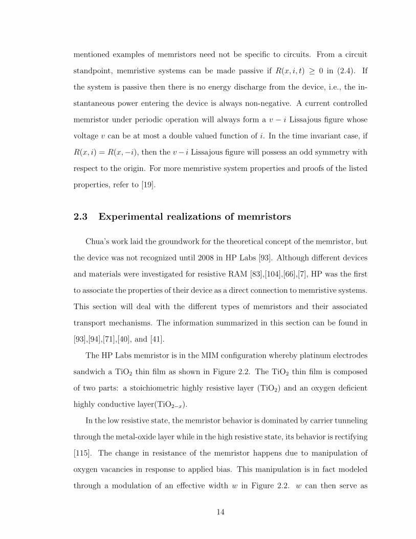
The HP Labs memristor is in the MIM configuration whereby platinum electrodes
sandwich a TiO2 thin film as shown in Figure 2.2. The TiO2 thin film is composed
of two parts: a stoichiometric highly resistive layer (TiO2) and an oxygen deficient
highly conductive layer(TiO2−x).
In the low resistive state, the memristor behavior is dominated by carrier tunneling
through the metal-oxide layer while in the high resistive state, its behavior is rectifying
[115]. The change in resistance of the memristor happens due to manipulation of
oxygen vacancies in response to applied bias. This manipulation is in fact modeled
through a modulation of an effective width w in Figure 2.2. w can then serve as
14

Figure 2.2: HP memristor device showing appropriate layers and identifying theohmic and non-ohmic contacts
the state variable in order to determine the transport characteristics of the device in
accordance with the definition of memristive system espoused in (2.5) and (2.4).
From device measurements [115], the fabricated memristor exhibits a rectifying
behavior, thereby suggesting that the non-ohmic contact at the Pt/TiO2 interface
influences electrical transport in the device. The oxygen vacancies in the TiO2−x side
make the TiO2−x/Pt contact an ohmic contact, allowing a model whereby a series re-
sistance can be attributed to this side of the memristor and a more complex rectifying
behavior is attributed to the other side of the memristor. Since tunneling through the
TiO2 barrier determines the current through the memristor, the non-ohmic interface
is said to dominate the transport mechanism of HP’s proposed structure. The value
of w is proportional to the time integral of the voltage applied to the memristor and
is normalized between 0 and 1 for the high resistive state and low resistive state,
respectively. The current behavior of the HP memristor is described by (2.6).
I = wnβsinh(αV ) + χ(exp(γV )− 1) (2.6)
In (2.6), the first term βsinh(αV ) is used to approximate the lowest resistive
state of the device, and α and β are fitting parameters. The second term of (2.6),
χ(exp(γV )− 1), approximates the rectifying behavior of the memristor with χ and γ
15
as fitting parameters. The value for n suggests a nonlinear dependence of the vacancy
drift velocity on the voltage applied to the memristive device. The value for n after
fitting parameters ranges from 14 to 22, thereby suggesting applied voltage exhibits a
highly nonlinear relationship with vacancy drift [115]. This highly nonlinear behavior
has led to several drift models using effective ion drift values.
The dynamics of w which completes the description of the HP thin film device as
a memristor is provided in [71] as (2.7a) and (2.7b)
w = foff sinh
(i
ioff
)exp
[−exp
(w − aoff
wc− |i|
b
)− w
wc
], i > 0 (2.7a)
w = fon sinh
(i
ion
)exp
[−exp
(w − aonwc
− |i|b
)− w
wc
], i < 0 (2.7b)
As with (2.6), parameter fitting is used to describe w, so foff , fon, ioff , ion, aoff ,
aon, b, and wc are the parameters to be set according to [71]. So with the dynamics
of (2.7a) and (2.7b) combined with the current description (2.6), the complete model
of the TiO2 memristor describing the specific HP device is complete.
Metal oxides are not the only candidates for memristive devices. In [40], the
memristor structure is composed of silver and silicon, specifically Ag/a-Si/p-Si. The
insulating layer is the a-Si while the contacts are Ag and heavily doped p-type crys-
talline silicon. The memristor state change in this device is achieved by the drift of
Ag ions towards the p-Si when voltage is applied to the device. The Ag ion drift into
the a-Si layer causes traps that lower the effective resistance of the entire device as
a whole. The ON to OFF resistance ratios of the a-Si memristor has been shown to
range from 103 to 107. With realized memristors, the models provided are mostly
parameters fitted to experimental results. This thesis takes a more generic approach
based on the work presented in [42]. The next section describes the memristor model
used for simulation.
16

2.4 Memristor modeling in this thesis
The memristor model used for simulation in this thesis is based on the nonlinear
drift model with window function Fp (2.9) as defined by [42] and [9]. The model is
based on the HP TiO2 device with the variables w and D identified in Figure 2.2 .
The doped region width w is modulated according to (2.8) with the window function
definition expressed in (2.9). For SPICE simulation the memristor model was im-
plemented as a functional block in Verilog-A with parameter p=4, memristor width
D=10 nm, and dopant mobility µD=10−9cm2/V · s.
dw
dt=µDRON
Di(t)F
(wD
)(2.8)
Fp(x) = 1− (2x− 1)2p (2.9)
The memristor’s resistance is viewed in the 2D framework, whereby effective resis-
tances of the oxygen deficient region (or doped region) and the effective resistance of
the undoped region are weighted and added. This linear combination is described in
(2.10), where ROFF is the resistance of the undoped region and RON is the resistance
of the doped region.
M(w) =w
DRON +
(1− w
D
)ROFF (2.10)
Joglekar and Wolf [42] performed two different derivations on the linear combi-
nation proposed. The first is dubbed the nonlinear drift model and is obtained by
combining (2.8) and (2.9) with (2.10) using integer parameter p > 1. The second
method is the linear drift model which is obtained by using an all pass window func-
tion which has the value of 1. The linear drift model provides the closed form analytic
model in (2.11), while the nonlinear model must be solved numerically.
17

MT = R0
√1− 2 · η ·∆R · φ(t)
Q0 ·R20
(2.11)
The memristance values over time follow the definition of MT in (2.11). In this
definition, MT is the total memristance, R0 is the initial resistance of the memristor, η
is related to applied bias (+1 for positive and -1 for negative), ∆R is the memristor’s
resistive range (difference between maximum resistance and minimum resistance),
φ(t) is the total flux through the device, and Q0 is the charge required to pass through
the memristor for dopant boundary to move a distance comparable to the device
width. So Q0 = D2/(µDRON), where D is device thickness and µD is dopant mobility,
as previously discussed.
Modeling and setup applied to Memory Chapter: The memristor crossbar is
an important element for ultra-dense digital memories. The crossbar structure has a
device at each crosspoint, therefore possessing the quality of a very dense device pop-
ulation compared to CMOS. The crossbar is composed of nanowires connecting mem-
ristors in a pitch width smaller than that of CMOS. The crossbar also scales better
than CMOS, thereby suggesting the process for building or fabricating this structure
is different from the standard CMOS process. For memory simulation (Chapter IV),
the crosspoint devices have diode isolation of individual devices in accordance with
[80]. The memristor is in series with a bi-directional diode model, representative of
the MIM diode. In order to model worst case effects, P-N diode model is used for
each direction of the bi-directional diode model, with each forward path presented in
(2.12).
IDiode = I0(e(qVD/(nkT )) − 1) (2.12)
Overall, the simulation parameters for the diodes were: I0=2.2 fA, kT/q=25.85
mV, VD is dependent on applied bias, and n=1.08. A P-N diode model is used because
18

it provides a weaker isolation than actual MIM diodes. Therefore, if the proposed
adaptive method works with P-N diode configuration, then it will work better with
actual MIM configuration that depends on tunneling currents and provides better
isolation than P-N diodes. Nanowire modeling for simulation is a distributed pi-
model, but for hand calculations, a lumped model will be used for simplicity. The
numbers used for the crossbar are per unit length resistance in order to obtain fair
results. From Snider and Williams [90], nanowire resistivity follows:
ρ/ρ0 = 1 + 0.75× (1− p)(λ/d) (2.13)
Where ρ0 is bulk resistivity, d is nanowire width, and λ is mean free path. The
nanowire recorded values used for simulation were: 24 µ · Ωcm for 4.5 nm thick
Cu. Following a conservative estimate in the memory application of Chapter IV, the
nanowire resistance was chosen to be 24 kΩ total. Using a nanowire capacitance of
2.0 pF·cm−1, the nanowire modeling was made transient complete.
Modeling and setup applied to Neuromorphic Work: For the neuromorphic
work (Chapter III), the memristor crossbar is not utilized, so individual memristor
characteristics are more important. Since the overall model is based on the HP Lab’s
device, a detailed valuation of a separation of the analog memristor is pursued as
opposed to the digital memristor. The memristor model of HP labs gives rise to
a device whose resistance change is proportional to applied bias. If applied bias is
relatively low for a certain time span, then the change in memristance is very small
and can be neglected. This idea allows for the establishment of a device threshold,
whereby the memristor’s resistance is assumed to be unchanged when bias is below
this threshold value. This memristor behavior is seen not just in HP’s device but
also in the a-Si memristor in [40]. The a-Si memristor shows conformity to the idea
of a built-in threshold, thereby allowing the authors to use different voltage biases
19

for read/write interpretation. This memristor can withstand low current without
resistance change, and this quality is important for analog circuit design usage of the
memristor.
The memristor behavior already described allowed for the creation of a threshold
based SPICE model proportional to conductance change magnitude, ∆C , that follows
(2.14).
∆C = −M × 3
√(Vab − Vthp)(−Vab − Vthn) + Voff (2.14)
In the above relationship, M is an amplitude correcting factor, Vab is the applied
bias across the terminals of the memristor, Vthp and Vthn are both threshold voltages
of the memristor with a positive and negative applied bias respectively. Voff corrects
and maintains a zero change with no applied bias. Equation 2.14 works really well
for a symmetric device, and the simulation done in this work uses a device with the
same magnitude in threshold voltage for both the positive and negative directions.
This threshold behavior, in conjunction with the linear-drift model presented in [42],
is used to implement a memristor with threshold characteristics.
The memristor threshold model does not assume zero change below the applied
threshold voltage. The change is minimal, but not negligible, to some above threshold
voltage applications as shown in a normalized plot of ∆C vs. Vab in Figure 2.3. In
circuit design, depending on application, the voltage choices between read and write
pulses will determine how the memristive device is used. The read pulse is chosen to
not cause drastic change in memristance, while the write pulse is chosen to encourage
higher levels of conductance change than the read pulse.
For hand design purposes, it is useful to determine appropriate pulse widths and
approximate memristance changes, for the change in memristance for each pulse is
very important. The exact role of the thresholding factor ∆C needs to be quantified.
By taking the derivative of (2.11) with respect to φ(t), the approximation of the
20

Figure 2.3: Normalized ∆C vs. Vab showing proportional magnitude of conductancechange as a function of applied bias. ±1 V can be viewed as thresholdvoltages
Figure 2.4: MT vs. φ showing two regions of operation for the memristor. In theslowly changing region, the magnitude of memristance change ranges from∼2 MΩ to 3 MΩ for every 1 Wb flux change. The change in memristanceincreases drastically when φ is > ∼2.5 Wb. (Parameters used to simulatethe analog memristor: R0=18 MΩ, Q0 = 5× 10⁻⁷ C, ∆R ≈ 20MΩ)
21

change of memristance is:
∆MT =−R0 · η ·∆R · φ(t)/(Q0R
20)√
1− 2 · η ·∆R · φ(t)/(Q0R20)·∆C (2.15)
Equation 2.15 suggests that for successive small changes in ∆φ whereby φ(t) is
not affected significantly, then the change in memristance, ∆MT , will respond with
almost constant step changes. For analog memristor design applications, the designer
is essentially taking advantage of this localized constant stepping for a range of φ(t)
values. The concept is represented in Figure 2.4 by graphing (2.11) with respect to
φ(t).
The plot in Figure 2.4 suggests an analog mode and a digital mode of operation
for the memristor. The mode of operation is strongly linked to the concept of lo-
calized constant stepping range previously discussed. In Figure 2.4, the decrease in
memristance seems nearly linear at first and then exponentially increases. The nearly
linear part of operation is where the memristor values should lie for the analog neural
network functionality. In this region of operation, φ(t) ≤2.6 Wb, the memristance
decreases by about 2 MΩ to 3 MΩ in response to every 1 Wb change in φ(t). This op-
erating region is a design choice to allow for better flexibility in choosing voltage levels
and pulse widths. Designs that desire higher changes with respect to chosen applied
biases will most likely operate in the region closer to the digital device characteristics.
2.5 Chapter Conclusion
Chua theorized existence of the memristor and formalized/defined the concept of
memristive systems to explain observed natural dynamics. When HP discovered the
memristor, research into resistive devices was spurred with multiple applications pro-
posed. The fabricated memristors are currently still under investigation with respect
to their transport properties, retention properties, device stability, yield, CMOS in-
22

tegration, etc. With these device specific issues in mind, architectural proposals of
device applications need to consider modeling techniques that encompass a range of
devices and materials, hence the model adopted for this thesis is one that exhibits
general physics theoretic properties that may be adopted to multiple devices (whether
analog or digital) through fitting parameters. From this generic model, training meth-
ods proposed in later chapters will be demonstrated.
23

CHAPTER III
Neuromorphic Building Blocks with Memristors
3.1 Introduction
Neuromorphic engineering is not a new approach to information processing sys-
tems. It particularly gained momentum in the 1980s with the amalgamation of learn-
ing rules and VLSI technology [97]. The growing transistor integration density in
CMOS enabled better simulation of neural systems in order to verify models and nur-
ture new bio-inspired ideas. Since then, the neuromorphic landscape has changed and
neuromorphic chips and programs are now available that cater to specific applications
and tasks.
Technological advancement has always been both friend and foe to neuromorphic
networks. Neuromorphic networks are essentially more valuable in instances where
parallel computing is necessary. In order to perform neuromorphic computing effec-
tively, a large number of processing elements (PE) is needed [97]. In current CMOS
technology, the density and connectivity required for more sophisticated neuromor-
phic systems does not exist. This has led many neuromorphic chips to implement
various schemes that utilize virtual connectivity between processing elements.
The shortcomings of CMOS in terms of density and parallel computing encour-
aged more complex neuromorphic system techniques and designs. Although design
complexity increased, the number of neurons, synapses, and connections that can
24

be simulated are orders of magnitude below the integration density of neurons in
the human brain. Human beings, possessing neurons that operate in the millisecond
range, can perform arbitrary image recognition tasks in tens to hundreds of mil-
liseconds, while very powerful computers would take hours, if not days, to perform
similar tasks. This lapse between digital computing and biology (specifically, the hu-
man brain) gives motivation for exploring technologies with connection densities that
surpass anything CMOS can offer.
Low power and high device integration in nanotechnology have reignited a spark
in the advancement of neuromorphic network in hardware as shown by Turel in [98]
and Zhao in [120]. The “Crossnets” approach shown in [98] provides evidence of the
design problems and methods of incorporation of resistive nanoscale devices in cross-
bar topology with CMOS circuitry to design neuromorphic circuitry. Nanotechnology,
specifically the memristor as postulated by Chua, shows much promise in this area
because it may overcome the inability to reach densities found in biological systems.
This inability is reduced by two factors: the first is the small size of the memristors
with respect to their functionality, and the second is the ability to connect the mem-
ristors with crossbars. Connecting these nano-devices (memristors) with nano-wires
(crossbars) has been shown to increase device integration significantly [92]. Device in-
tegration in MMOST (Memristor-MOS Technology) is expected to improve in the age
of memristors and crossbar scaling. A hypothetical study of a cortex-scale hardware,
performed in [119], shows the use of nano-devices in a crossbar structure has the po-
tential of implementing large-scale spiking neural systems. More complex algorithms
like Bayesian inference [118] have also been studied for crossbar implementation, but
these studies limit the crossbar array to digital storage. Analog use of the array would
be ideal to reap its full benefits.
Neuromorphic networks derive their behavior from learning rules [15]. The net-
works have inherent governance that maintains relationships between neurons and
25
synapses. Based on the myriad of combinations of synaptic weights and neuron be-
havior, the network at any given point in time is unique.
The goal of this chapter is to show that memristors are valuable in the devel-
opment of biologically inspired adaptable circuitry. Three identified behaviors, well
documented with biological neurons, will be introduced. These are lateral inhibition,
spike timing dependent plasticity (STDP), and inhibition of return (IOR). An ap-
proach to implementing these behaviors with memristors will be discussed. These
behaviors are fundamental building blocks for neural hardware that have been well
demonstrated in CMOS. This chapter will show a new, compact way of implementing
STDP compared to pure CMOS. In addition, the chapter will also provide a method
of realizing a reconfigurable XOR gate. The XOR gate is provided as an example,
for in order to build more complex systems, both analog and digital methods will
most likely be implemented. No specific recommendation is made for integration of
analog/digital neuromorphic circuit blocks.
3.2 Implementing Neuromorphic Functions with Memristors
3.2.1 Lateral Inhibition
Lateral inhibition is seen prevalently in the biological world. This phenomenon has
been credited with playing a part in amplifying variation in gradients [102], signaling
orientation for vision processing and sensations [10], and providing form and structure
during development and neurogenesis [55]. The inhibition process, a simple idea,
seems to play a role in biological processing to create complex schemes and structures
such as leaf patterns on trees, branch formations, and limbs on various organisms.
The importance of inhibition for biological processing cannot be discounted. Although
the inhibition process might seem a simple idea, its deconstruction from biological
systems has not been so straightforward.
26

Inhibition plays a key role in neuron processing, so artificial neurons need to
exhibit this behavior to closely approximate their biological counterparts. The lateral
inhibition in artificial neural architectures exists as either total inhibition (as in the
case of McCulloch-Pitts neurons [54]) or partial inhibition (as in the case of the
perceptron [82]). Examples of these include the contrast enhancer using cross coupled
transistors [109] and the winner-take-all (WTA) circuitry[67][99][85][36][73] that may
be used for self-organizing maps [17]. These examples show that lateral inhibition
has progressed and has been realized in neuromorphic hardware research. Adoption
of memristor crossbar should further encourage and support the ease with which the
inhibition process can be achieved since the lateral inhibition with memristors in
crossbar simplify the circuitry and wire connections necessary with CMOS.
Lateral inhibition as well as recurrent network configurations can be achieved
with memristors as shown in Figure 3.1. The memristor crossbar allows massive
connectivity from one neuron to another through modifiable weights. Neurons in the
same functional vicinity can be made to inhibit one another through the crossbar
configuration. For example, N11 is connected to N12 through some synapse M1112;
the signal injected through this synapse M1112 from N11 will be an inhibitory signal
that will disturb the internal state of neuron N12. This crossbar method can also
be extended to excite neighboring neurons. In this neuromorphic approach, two
memristor crossbars can be stacked upon one another: one for excitatory synapses
and the other for inhibitory synapses.
In addition to lateral inhibition, self-enhancement seems to play a key role in
neurogenesis [55]. An effect measured in biological neurons seems to be lateral inhi-
bition of neighboring neurons but self-enhancement of oneself. This effect prevents a
feature or neuron from inhibiting itself. For example, when a leaf forms on one part
of a branch, an area around the leaf receives an inhibitory effect that suppresses the
formation of other leaves too close. Since this inhibitory effect applies to an area that
27

Figure 3.1: Recurrent network architecture showing an example of how Winner-Take-All, lateral inhibition, or inhibition of return can be connected using cross-bars
includes the inhibiting leaf itself, in order to combat its inhibitory effect, the leaf has a
positive feedback loop that reinforces its continued development and existence. This
self feedback loop can be made with the memristor crossbar as shown in Figure 3.1.
3.2.2 Inhibition of Return
IOR, in its hardware implementation, is a neuromorphic algorithm used to allow
different neurons to spike [44]. From the previous section, lateral inhibition imple-
menting WTA only allows for one neuron to be considered the winner when in com-
petitive spiking with its neighbors. By combining WTA with IOR, the behavior of the
winner changes, for successive neurons will take the winner’s place after a designed
time period. By implementing this combination, the winner inhibits itself after an
allowed spike duration and gives rise for another spiking neuron to win. This algo-
rithm can be used to map network activity as well as compare different input pattern
intensities. No surprise, it is mostly used in visual neuromorphic applications, such
as attention shifts [61].
Memristor MOS Technology (MMOST) design of IOR can be accomplished in a
similar way as the WTA. The self-feedback parameter (synapse) would be strength-
28

ened so the neuron will inhibit itself strongly as its spiking frequency increases. The
neurons with the strongest synaptic inhibitions (lowest synaptic weights) can be com-
pared with one another with respect to synaptic strength in order to determine the
current relationship between them.
3.2.3 Coincidence Detection
Coincidence detection occurs when two spiking events are linked and coded for in
a certain way. This algorithm is usually found in pattern recognition or classification
systems, whereby the neuromorphic network codes differently an input train of pulses
or spikes. Based on the level of coincidence between different inputs to the network,
the neural network responds appropriately. This realization is not the only way to
use coincidence detection.
Another way to use coincidence detection is to update synaptic weights based on
coincidence. This relates to the plasticity of the synapse and governs the learning
rule of the synapse locally. In this form, the coincidence detection is known as STDP
[24]. There are two main forms of STDP: symmetric STDP and asymmetric STDP
(as depicted in Figure 3.2). Symmetric STDP performs the same weight adjustments,
independent of the spike order between the pre-neuron and the post-neuron, while
asymmetric STDP reverses weight adjustment based on the spike time difference
between the pre-neuron and the post-neuron.
STDP implementations utilizing the crossbar structure have been proposed [89],[50],[1].
In their current state, they do not provide much density gains when comparing
MMOST to CMOS. The implementations require pulse/signal generations in both
the positive and negative directions across the memristor. Snider [89] proposes a
decaying pulse width while Linares-Barranco and Serrano-Gotarredona [50] and Afifi
et al [1] propose decaying signal amplitudes. All three suggested implementations
rely on the additive effect of the signals across the memristor to control the synaptic
29

weight changes. The STDP synaptic weight implementation in this thesis is realized
with a different approach; pulses are used to make a linear approximation of the
STDP curve in order to reduce the size of the neuron.
The proposed STDP implementations are usually of the form in Figure 3.2. These
synaptic behaviors, both asymmetric and symmetric, have been implemented in
CMOS [96],[37],[11]. In the asymmetric STDP case, if the pre-neuron spikes before
the post-neuron, the synaptic weight is increased. If the order of spikes is reversed, the
synaptic weight is decreased. In both cases, the larger the duration between the pre-
neuron and the post-neuron spikes, the lesser the magnitude of the synaptic change.
Most circuit implementations take advantage of the asymmetric implementation.
The STDP implementation in this work is asymmetric and is based on the equation
in the form of (3.1):
4W (t2 − t1) =
A+e−(t2−t1)/τ+ , t2 − t1 > 0
−A−e(t2−t1)/τ− , t2 − t1 < 0
(3.1)
The change in synaptic weight,4W , is dependent on spike time difference between
the pre-neuron and the post-neuron, t2 − t1. A+ is the maximum change in the
positive direction, A− is the maximum change in the negative direction, and both
changes decay with time constants τ+ and τ−, respectively. Most implementations
use capacitors and weak inversion transistors to adjust τ+ and τ− in order to obtain
decay times in the hundreds of milliseconds [45]. An alternate way to realize STDP
in CMOS when working under a lower area budget is to incorporate digital storage
units that can help remember spike states instead of using huge analog capacitors to
set time constants.
The total change in weight for a given synapse is the summation of all positive
and negative weight changes. Over the learning period, the synapse will converge
to a certain weight value and will remain stable at that value. The STDP concept
30

Figure 3.2: STDP curves showing relationship between synaptic weight change andthe difference in spike times between the pre-neuron and the post-neuron.Symmetric STDP and Asymmetric STDP are both found in nature [23].
31

Figure 3.3: Neural network implemented in Verilog in order to determine noisy per-formance of STDP in comparison to digital logic
was tested through Verilog simulations, whereby STDP was pitted against digital
computation to do a comparison under noisy conditions.
The network of interest for simulation was that of a 1D position detector, where
the location of an object is determined by the two-layered neural network presented
in Figure 3.3. The network consists of an input neuron layer (neurons labeled n11
through n15) connected through feedforward excitatory synapses to an output neuron
layer (neurons labeled n21 through n25). At the output layer, each output neuron is
connected to every other output neuron through inhibitory synapses.
The network shown in Figure 3.3 updates its synaptic weights through STDP.
Both excitatory (gray triangles) and inhibitory (red triangles) synaptic weights are
modified through STDP. The inherent competition resulting when the output neurons
spike help establish the weights for all 20 inhibitory synapses. An object is presented
to the line of input neurons shown in Figure 3.3. The object’s presence generates
signals that affect the closest neurons to its position. For example, if the object is
directly in front of n13, then only n13 receives the object’s generated signals, but if the
object lies between n13 and n14, then both n13 and n14 receive the input signals. The
32

object’s position is deciphered from the output neuron based on the relative spiking
frequency (or period) of the output neurons.
The 1D position detection was simulated for two noise conditions — noise-free
condition and noisy condition — with different object locations. The noise-free case
results are trivial. If there is no noise in the input of the system, then the output
neuron results can be reduced to binary outputs — spike or no spike. For example,
in the noise free case, an object placed next to n13 causes n23 to spike while the other
input and output neurons do not spike. In this noise free case, the implementation
of this position detection function could have been accomplished with digital logic
where input signals exceeding some threshold would provide the desired output. In
the noise-free case, when the object is placed between n12 and n13, both n22 and n23
spike but the relationship between their spiking frequencies is proportional to the
input object’s exact location between both n12 and n13. If the object is closer to
n13, then the spiking frequency of n23 is a little greater than that of n22. The noise
free condition provides direct mapping of either a spike or a no spike with neurons
involved in receiving the object’s input and those not receiving the object’s input.
The noisy condition case is a bit more interesting, and the results are summarized
in Table 3.1. Table 3.1 provides results for the noisy case whereby all neurons in
the output layer spike due to the noise background effect fed in through the input
layer. The units in the simulation are time units or simulation time steps. Period is
determined after weight stabilization has occurred and the time between successive
spikes becomes fairly regular. The object’s position can be determined in all three
cases presented in the table. When the object is at n13, n23 spiking period is the
lowest (n23 is spiking the most). When the object is between n12 and n23 but closer
to n13, n23 spikes the most but its spiking period is comparable to n22. A second level
processing can compare these two neurons’ spiking period to determine the object’s
location relative to the two neurons that spike the most. Lastly, when the object
33

Period (time between successive spikes)OutputNeurons
Object at n13 Object betweenn12&n13 but closerto n13
Object midway be-tween n12&n13
n21 1746 2046 1014n22 786 684 660n23 636 642 660n24 786 3030 1506n25 1746 7242 7266
Table 3.1: Verilog STDP Output Neuron Results for an Object Placed at DifferentLocations on the 1D Position Detection Line
is exactly midway between n12 and n13, then both n22 and n23 spike with the same
spiking period.
An extension of these results may be used for motion detection. Looking at the
spiking response of n23, we may conclude that the spiking period decreases as the
object moves away from n13. The advantages therefore seen in using STDP is that
by determining the object’s position using the spiking frequency, the neural network
can withstand the effects in a noisy background while digital threshold logic fails.
3.3 CMOS-Memristor Neuromorphic Chips
The validity of memristors as processing elements is investigated using two neu-
romorphic architectures that exhibit lateral inhibition as well as STDP. The first
architecture is for a local “position detector” and the second architecture is a multi-
function chip that can be trained to perform digital gate functions such as the XOR
function. The XOR function is later extended to perform edge detection.
3.3.1 Analog Example: Position Detector
Procedure: Given a two dimensional area, split up the area into a 5x5 grid Fig-
ure 3.4. Each square on the grid represents the resolution for the detector. A neuron
resides at the center of each square on the grid. The detector has a two dimen-
34
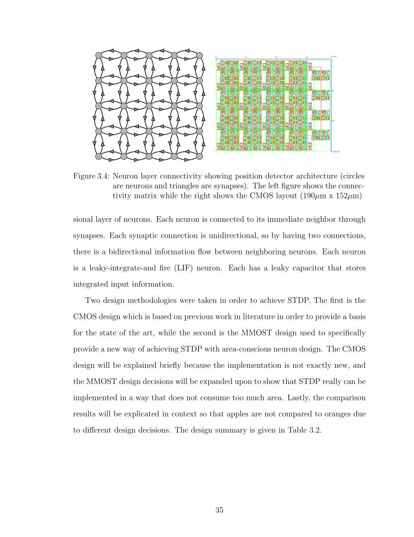
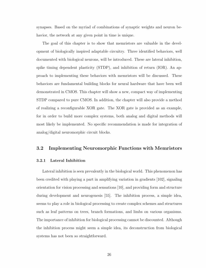
Figure 3.4: Neuron layer connectivity showing position detector architecture (circlesare neurons and triangles are synapses). The left figure shows the connec-tivity matrix while the right shows the CMOS layout (190µm x 152µm)
sional layer of neurons. Each neuron is connected to its immediate neighbor through
synapses. Each synaptic connection is unidirectional, so by having two connections,
there is a bidirectional information flow between neighboring neurons. Each neuron
is a leaky-integrate-and fire (LIF) neuron. Each has a leaky capacitor that stores
integrated input information.
Two design methodologies were taken in order to achieve STDP. The first is the
CMOS design which is based on previous work in literature in order to provide a basis
for the state of the art, while the second is the MMOST design used to specifically
provide a new way of achieving STDP with area-conscious neuron design. The CMOS
design will be explained briefly because the implementation is not exactly new, and
the MMOST design decisions will be expanded upon to show that STDP really can be
implemented in a way that does not consume too much area. Lastly, the comparison
results will be explicated in context so that apples are not compared to oranges due
to different design decisions. The design summary is given in Table 3.2.
35

3.3.1.1 CMOS Design Description
The CMOS design has an LIF neuron with multiple inputs depending on the
location within the position detection fabric. The neuron is inspired by designs with
complimentary inputs, which has PMOS (pull ups) for excitatory inputs and NMOS
(pull downs) for inhibitory inputs. Each neuron has only one pull up and multiple pull
downs depending on the location in the position detector fabric, e.g., 4 pull downs
for neurons surrounded by 4 neighbors. The STDP synapse approach is similar to
those already presented in literature [96],[45] and the synapse schematic is shown
in Figure 3.5. When the pre-neuron spikes, Spre activates a switch that charges
C1. When Spre deactivates, C1 discharges exponentially, but the capacitor CWeight
is not updated until there is a post-neuron spike event. A post-neuron spike event
would activate Spost, therefore allowing the evaluated output of the top comparator
to see CWeight. This explained sequence describes long term potentiation (LTP).
The post-spiking before the pre-spiking would entail long term depression (LTD). To
reduce area, the capacitors C1 and C2 were implemented with diode connected NMOS
transistors operating in weak inversion. The voltage range between Vcharge and VQ is
made to be about 100 mV. The decay shape of the voltages across C1 and C2 from
Vcharge to VQ is a function of the difference between Vcharge and VQ. By reducing the
voltage range, the decay appears more linear than exponential.
3.3.1.2 Memristor-MOS Design Description
The MMOST design will be delved into with more detail than the CMOS design.
The design goal is to take advantage of the memristor crossbar, thereby simplifying the
synapse and making it a fraction of the size of the CMOS synapse. The synapse itself is
a simple memristor whose changes respond to pulses of equal widths provided through
the neurons. STDP mechanism is moved from the synapse to the neuron. The neuron
design utilizes a new way of realizing STDP by striking a tradeoff between neuron
36

Figure 3.5: STDP Synapse Circuit Diagram implemented in CMOS
area and asynchrony. The neuron implementation of STDP is depicted graphically in
Figure 3.6. The STDP behavior modeled is based on a linear approximation behavior
observed in mushroom bodies as shown in [14].
Figure 3.6 shows the spike patterns between a pre-neuron’s output and a post-
neuron’s input (the memristor lies between these two terminals). In Figure 3.6, the
pre-neuron spikes right before time t0, so at time t0, the pre-neuron’s output is at 0V.
The 0V level is held for 4 clock cycles (from t0 to t3) then pulses are allowed to pass
for another 4 clock cycles (from t4 to t8). Afterwards, the pre-neuron’s output rests
at a reference voltage, VREFX . The post-neuron’s input exhibits a similar behavior
as the pre-neuron’s output, but instead of spiking before time t0, it spikes sometime
in the interval from t2 to t3. The post-neuron’s input is pulled to 0V at time t3, as
opposed to time t0 as the pre-neuron’s output. The pre-neuron’s output and the post-
neuron’s input spiking patterns present a difference across the memristor’s output,
and this difference is shown in Figure 3.6 as “pre”-“post”. As explained earlier, the
memristor utilized is a threshold device, meaning its conductance experiences greater
37

Figure 3.6: Pre-neuron and post-neuron spiking diagram showing three pulses abovethe memristor’s threshold. The below threshold pulses do not greatlyinfluence conductance
Figure 3.7: Neuron circuit that can provide spiking pattern for STDP realization withmemristors
change when a voltage greater than its threshold voltage, vth, is met. The threshold
is exceeded only by the three pulses shown in Figure 3.6. The neuron circuit that can
implement the spiking patterns depicted in Figure 3.6 is shown in Figure 3.7.
The neuron in Figure 3.7 is composed of an integrate and fire circuitry, a path for
passing an inhibitory current signal Iin to the integrate and fire circuitry (pass), paths
for pulling the neuron’s input and output nodes high (adj1), and paths for pulling
both its inputs and output nodes low (adj2). The control signals (pass, adj1, and
adj2) to turn each path on is controlled by the Finite State Machine (FSM) shown
in Figure 3.8.
38

Figure 3.8: FSM showing control signal generation
In Figure 3.8, Start is the default state — the neuron is not spiking, the neuron’s
input and output voltages are at reference voltage (VREFX), pass is ON, adj1 is OFF,
and adj2 is OFF. When the neuron receives excitatory inputs from the environment
enough to cause a spike, then spike becomes 1, and in the next clock cycle, the neuron
moves to the next state, Low. In the Low state, both the input and output ports of
the neuron are pulled to 0 V — the neuron has spiked, pass is OFF, adj1 is OFF,
and adj2 is ON. The neuron stays in this state for 4 clock cycles (a counting variable
increments from 0 to 3) before moving to the Pulse state. The Pulse state is the state
where the neuron passes the external pulse to both its input and output ports —
pass is OFF, adj1 is ON, and adj2 is OFF. In order to move from Pulse to Start, a
counting mechanism is employed for 4 clock cycles. This internal FSM resides within
each neuron.
3.3.1.3 Comparison of CMOS Design and Memristor Design
CMOS MMOSTTiming Asynchronous Clocked (1 kHz)Power (Static, Dynamic max) 0.2 µW, 55 µW 5.28 µW, 15.6 µWChip Area 2.89× 10⁻⁴ cm2 6.1× 10⁻⁵ cm2
Input Noise(0.3V noise level) > 3 dB SNR > 4.8 dB SNR
Table 3.2: Design summary for both proposed WTA CMOS and MMOST 5X5 Posi-tion Detector Arrays
The CMOS design is an asynchronous design in which minor perturbations on a
39

neuron’s excitatory input can cause a spiking event. The MMOST design is a clocked
design that synchronizes OFF-chip signals with the ON-chip logic. The MMOST
design itself has asynchronous parts to it (neuron integration and signal input), but
the timing of change in resistance of the memristor is a synchronous event. The
WTA algorithm allows for spiking neurons to inhibit one another while changing
synaptic weights to strengthen or weaken the inhibition. The change of synaptic
weight for both the CMOS and memristor or MMOST design qualifies as the ability
for the chip to learn. The advantage of choosing an STDP design is to take advantage
of its noise handling capability. The lower the noise level, the lower the difference
between signal and noise necessary for position detection. In comparing the CMOS
and MMOST designs, the MMOST design has a higher potential because consumes
less area and requires less operating power. The quoted values in Table 3.2 for the
MMOST design for both power and area are over-estimations, so the possibility of
improving over CMOS with this technology is very appealing. This is without even
considering potential synaptic and neuronal densities that can be achieved. The
local connections adopted for this example are beneficial for the CMOS numbers
but increasing the neighborhood connections will have a larger detrimental effect on
CMOS density than on MMOST density.
Design Complexity: For the current implementation, the timing of the CMOS
circuitry is designed to perform STDP in the tens of microsecond range in order to
conserve area. This value can be adjusted by using bigger capacitors (C1 and C2 in
Figure 3.5) to extend the time constant or by putting the synaptic transistors (those
that implement switches and comparators) even more into subthreshold. The CMOS
design can become very complex when trying to design for its most dismaying feature:
volatility. Currently, when the stimulus is removed, the weight decays exponentially to
its DC steady state in about 100 ms, since synaptic weight is stored on capacitors. A
40

way to improve this design would be to save these weights to memory and incorporate
read, write, and restore schemes which requires careful timing requirements.
The Chip area (5x5 array) for the CMOS design is about 2.9× 10⁻⁴ cm2 from the
CMOS layout, while that for the MMOST is about 6 × 10⁻⁵ cm2. The memristor
design area is an over-estimation, so it is likely to be much less than the proposed
value. From design automation, the current logic for the memristor design is expected
to take about 488 minimum sized transistors. Since this automated design was not
simulated for signal integrity, drive, etc., for a worst case scenario, we double this
value by 2 in order to account for various signal buffering, clock signal regeneration,
and via spaces to the crossbar structure. This gross estimation still shows that the
memristor design consumes 5 times lower area than the CMOS design. This value can
only improve, for a custom design would use fewer transistors. The area estimation
assumes that the crossbar array area will be fully contained over the CMOS area.
Power: The CMOS design consumes less static power than the memristor design,
mostly due to the fact that both designs are operating under different supply voltages
(1 V for CMOS, 1.5 V for MMOST), and the memristor design has only a few tran-
sistors operating in the weak inversion region. The operating voltage difference is due
to the fact that memristors will need to exceed a threshold voltage in order to change
resistance, and the largest voltage across the memristor with under the 1.5 V power
supply is about 0.9 V. The static power can be reduced for later generations of the
design by having a lower voltage supply and using charge pumps to achieve required
threshold voltages. Although the static power consumption for CMOS is lower, its
maximum dynamic power is higher than that of the memristor design. The memristor
design consumes 15.6 µW while the CMOS design consumes 55 µW. The memristor
logic and comparators use most of the power due to heavy switching during spiking
events. In the case of CMOS, as neurons begin to inhibit one another, they create
41

or strengthen paths to ground allowing larger current draw especially when both ex-
citatory and inhibitory inputs are activated. This current adds up pretty quickly as
array size increases.
Noise: Both the CMOS and memristor designs were tested with a noise background
between 0.1 V and 0.3 V. The conclusion for testing under CMOS is as noise level
increases, the required signal level to counter this noise also increases. For example, at
a noise level of 0.2 V, as long as the signal is at least 0.3 V, the neuron of interest will
spike accordingly. This is a 100 mV difference between signal and noise. This value
changes to 125 mV with the noise level increases to 0.3 V. In real world computing, we
do not expect the noise to be quite that high, but as long as the signal level is above
0.425 V, the neural network will work as designed. For the memristor design, the
noise level is actually used to randomly assert the memristors at different conductance
states. Once the network is stabilized under a certain noise level, the signal input is
capable of tuning the memristors around its signal level for the detecting purpose.
The noise levels used for simulation are similar to that of the CMOS design (0.1 V,
0.2 V, and 0.3 V). At 0.3 V, as long as the input is about 200mV greater than the
noise level, then the signal is discernible.
3.3.2 Digital Example: Multi-function Chip Architecture
The previous example showed that through analog computation, localized signal
detection can be computed. This section will show that digital functions can also be
achieved with the proposed neuron design. The approach that will be presented may
actually use more area than a digital approach would require, however the current
approach can be reconfigured and can also interface well with other analog compo-
nents. The multi-function chip architecture is shown in Figure 3.9. The neurons are
shown in circle and implemented in CMOS while synapses are shown with arrowed
42

Figure 3.9: Neuromorphic architecture for the multi-function digital gate showingneurons and synapses
lines and are implemented with memristors. Excitatory synapses are in red, and
inhibitory synapses are in black. The architecture is amenable to STDP synapses
whereby the spike timing between pre-neuron and post-neuron determine how much
the memristive synapses will adjust. The same approach to achieving STDP is used
with this architecture as in the position detection architecture.
The neuromorphic architecture is composed of both input and output neurons, and
based on the chosen structure of inhibitory to excitatory synapses, various functions
can be obtained. The XOR and Edge Detector have the same synaptic weight profile,
but perform different functions. An AND or an OR gate would have a different
synaptic profile than both XOR and Edge Detection. The basic architecture shown
needs pre- and post-processing circuits to interface with other systems. The post-
processing side may contain adders and integrators to convert spiking outputs of the
spiking neurons to leveled signals, while the pre-processing side would convert DC
level signals to spiking inputs for the neurons. Each function will have different post-
43

processing requirements; the architecture is meant to be the barebones to allow for
different functionality based on synaptic weight adjustments.
The training process involves using input patterns in order to adjust memristors to
the desired relative values between excitatory and inhibitory synapses. On simulation
startup, weights can either be initialized to a low value, or initialized to a random
pattern and learned to low values. Using different input patterns, the memristors
can be trained to predetermined weights or relative weights between excitatory and
inhibitory synapses. For example, starting in a low weight state, n11, n13, and n15 can
be made to spike at frequencies that cause n21, n23, and n25 to spike, thereby strength-
ening excitatory synaptic connection between these neurons according to STDP rules.
This input pattern will not affect the inhibitory synapses due to the rules of STDP
requiring pre-neuron and post-neuron to spike. After these synapses are trained to
weights approximately twice the inhibitory synaptic weights, neurons n12, n14, and
n16 are used to train the excitatory synapses between n22, n24, and n26.
This training scheme is designed for the XOR and edge detection profile and allows
the tuning of excitatory synapses without affecting inhibitory synapses as shown in
Figure 3.10. The synapse naming follows the convention “pre-neuron post-neuron”.
In Figure 3.10, the XOR training is done for 30 ms to get a resistance profile for the
excitatory neurons around 5.6 MΩ. The tuning of the memristors to exact resistance
values is hard to accomplish, therefore, in a system, a timer would be used to stop
training. This training scheme hints that the neurons have two different modes de-
termined by a control signal deciding on either a training mode or running mode.
The difference between the two modes lies in the voltage levels used for both. The
training mode uses voltage levels that influence the memristors more than the running
mode. The simulation results shown for the XOR and edge detection operation use
the learned memristor resistance values of about 10 MΩ and between 5.6 to 6.8 MΩ
for the inhibitory synapses and the excitatory synapses, respectively. The simulation
44
Figure 3.10: Training mode using prescribed XOR training scheme (Top) Inhibitorysynapses unchanged during training (Bottom) Excitatory synapsetrained using timestamps
45

Figure 3.11: XOR simulation results showing: (a) Input A (n11 and n12) = 0, andInput B (n13 and n14)= 0, so Output (n22 or n23)= 0. (b) Input A = 0,and Input B = 1, so Output = 1. (c) Input A = 1, and Input B = 1, soOutput = 0. (d) Input A = 1, and Input B = 0, so Output = 1
results are shown in the run-mode — learning has stabilized, and voltages adjusted
so memristors are fairly static.
XOR Simulation: The neuromorphic architecture is simulated in Cadence Analog
Environment with IBM 90nm CMOS9RF process. The XOR simulation setup does
not use all six input-output neuron pairs. Four neuron pairs are needed for the XOR
operation. For example, to find the XOR between logic signals A and B, input A
would be given to n11 and n12 while input B would be passed on to n13 and n14.
The outputs would be read from the sum of n22 and n23. Figure 3.11 provides the
results for the XOR operation for all cases. Figure 3.11a provides results for the case
when both inputs A and B are Logic “0” thereby producing no spiking behavior at
the outputs. Figure 3.11b and Figure 3.11d provide the scenarios when one input is
Logic “1” and the other input is Logic “0”.
In Figure 3.11b, Input A is Logic “0” and Input B is Logic “1”. The result from
46

the simulation shows that n23 spikes in a pattern that signifies Logic “1” while n22
does not spike at all. The XOR post processing will integrate and add the results
of n22 and n23 to obtain a final verdict. The spiking behavior of either n22 or n23
should be deciphered as a Logic “1” by the post-processing circuitry. Figure 3.11d
provides results and works in a similar way to Figure 3.11b except this time, instead
of n23 spiking and n22 not spiking, n23 does not spike but n22 spikes. The results from
post-processing will be the same as the previous case.
Lastly, Figure 3.11c shows the case when both inputs A and B are Logic “1”. The
results show that neither n22 or n23 spikes therefore providing output results similar
to Figure 3.11a. As expected, the XOR operation is verified with all test cases and
shows that the neuromorphic architecture works as expected. Due to the bidirectional
nature of the output node, Logic “0” when inputs do not induce spiking is different
from Logic “0” when inputs induce spiking. For example, the Logic “0” seen for n11
and n12 in Figure 3.11d looks different from that of Figure 3.11a. The disturbance
seen is directly related to the spiking behavior of the second layer of neurons. The
pulses from this layer directly cause a disturbance in the output node of the input
neurons.
Edge Detection Simulation: The edge detector operation is similar to XOR as
shown in Figure 3.12. In Figure 3.12, the input neurons n11,...,n16 receive “011110”
respectively, and they cause the output neurons n21,..., n26 to produce “010010”
respectively. In the input pattern, there are two edges, i.e., between n11 and n12 and
between n15 and n16, and the neural network configuration was able to extract these
edges in the output spiking pattern. The post-processing on the edge detector will
integrate each output to determine output logic level. The verification of the edge
detector is done by showing another pattern with input neurons n11,...,n16 receiving
“100110” respectively. This pattern clearly has two edges between n13 and n14 and
47

between n15 and n16. Another observation here is that since there is no wrap-around
effect in the neural architecture, the neural network identifies Logic “1” values at
the extremes as edges. This design decision is architecture dependent and behavior
may be changed by modifying the synaptic weights of the synapses controlling neuron
behavior at the extremes. The result for the input pattern “100110” turns out to be
“100110” and the post-processing for the edge detection should be able to extract the
position of the edges quite clearly.
The CMOS neuron from the position detector is scaled down from 130 nm CMOS
process to 90 nm. In addition to process migration, the inclusion of synaptic weight
dependent excitatory inputs was made. The neuron design was migrated from a
mostly saturation design to a mostly subthreshold design to improve power efficiency.
When conducting the simulation for edge detection and XOR, the average power
consumption per neuron during the spiking is about 0.3 µW, which is more than an
8X saving over our position detector neuron.
3.4 Chapter Summary
We have explored the benefits of moving to an MMOST design for STDP circuit
implementation on the bases of circuit area, power, and noise. The area considerations
are implementation dependent, but scaling to denser networks favors the MMOST
design, for a CMOS implementation will require more STDP synapses, which greatly
limit connectivity. The power considerations show mixed results because moving to
synchronous STDP for the MMOST implementation may actually waste more power
in the idle state than the CMOS implementation. Dynamic power numbers are better
for MMOST, so a more active circuit would take advantage of the MMOST design.
The noise considerations show that both designs are comparable. However, this may
change with device scaling, as both memristors and CMOS transistors become more
susceptible to noise.
48

Figure 3.12: (Left) Edge detection simulation results for input pattern “011110” pro-duces output pattern “010010”. (Right) Edge detection simulation re-sults for input pattern “100110” produces output pattern “100110”
In addition to the STDP circuitry, a neuromorphic architecture for digital compu-
tation is proposed. The architecture is shown to perform the XOR and edge detection
operations after a supervised learning process. The design is simulated in 90 nm IBM
CMOS process with power consumption while spiking at 0.3 µW. The amenable archi-
tecture is great for the memristor crossbar design, allowing the area savings possible
with building crossbars above CMOS circuitry. The overall purpose of this work is
to explore low level computing components that can utilize nanodevices in a man-
ner that encourages parameter adjustment in order to facilitate on-site tuning when
necessary.
49

CHAPTER IV
Memristor Digital Memory
4.1 Introduction
In the process of developing highly dense computing systems, the problem of dense,
low power, non-volatile memory still remains. This section discusses the difficulties
currently present in memristor memories and provides an adaptive method to tackle
those difficulties.
The memristor memory is a viable candidate for future memory due to the diffi-
culties encountered with CMOS scaling. However, memristors have their own com-
plications to realizing this memory system. The patent database provides a myriad
of methods to deal with difficulties (resistance drift, nonuniform resistance profile
across the crossbar array, leaky crossbar devices, etc.) that arise from working with
these resistive memory elements. These difficulties (problems) are addressed within
the database by using correcting pulses to mitigate the effect of resistance drift due
to normal usage [60]; using a temperature-compensating circuit to counter resistance
drift due to temperature variation [35]; using an adaptive method to read and write
to an array with nonuniform resistance profile [91]; and introducing diodes [63] or
metal-insulator-metal (MIM) diodes to reduce leaky paths within the crossbar mem-
ory array [80].
With every proposed solution to solve a problem, there are drawbacks that need to
50

Figure 4.1: Memory system top-level block diagram
be considered. The work in this chapter exposes a view that may lead to the realiza-
tion of memristor based memory in the face of low device yield and the aforementioned
problems that plague memristor memory. Section 4.2 describes the reading, writing,
and erasing methodology; Section 4.3 shows the simulation results; Section 4.4 ex-
plains the results; and Section 4.5 provides concluding remarks.
Figure 4.1 shows the top level block diagram of the envisioned memory architecture
and the connections between the crossbar array and the periphery circuitry. The Row
Address and Column Address signals allow a selected row or column to be transparent
to either the RC (Read Circuitry) or the Data sections.
The nature of the muxes may prove to make design more difficult due to the
stringent requirements of their functionality. These requirements do not affect the
muxes controlled by the RP (Reverse Polarity) signal; these muxes are simpler, as
they are essentially transmission gate muxes that switch between two paths. For the
Row and Column Address muxes, the mux requirements extend beyond switching
51

paths for unselected and selected lines. Our preliminary simulations agree with the
results from [79], proposing active bias for unselected lines (columns and/or rows).
When a line is unselected, a reference bias must be set on all the unselected lines,
thereby limiting the leakage paths that may affect read and write integrity. For more
details on this problem, refer to [22]; this reference discusses in detail the effect on
noise margin of floating the unselected lines in a resistive memory.
In this implementation, the selected and unselected lines have two different refer-
ences corresponding to when the memory is in use and when the memory is not in
use. When in use, the unselected lines are held at VREF voltage, and when not in
use, the lines are grounded. The selected lines pulsate between VREF and VDD when
memory in use but is held to ground when memory is not in use. The signal flow is
unidirectional from Data, through an RP mux, through a Mux/Demux, through the
MCA (Memristor Crossbar Array), through another Mux/Demux, then another RP
mux, and finally to the RC. The signal flow direction is controlled by which RP mux
is connected to the RC and which is connected to Data.
Data is a small driver that asserts VDD. The length of time VDD is asserted is
controlled by timing circuits that determine when to open the signal path from Data
to RC. The RC block is essentially a generic block that implements the flow diagram
represented in Figure 4.2, specifically, the “Calculate δ” and the steps that lead to
determining the logic state of the selected memristor device. This signal flow is used
to avoid negative pulse generation signals as seen in [33] and [65].
4.2 Adaptive Reading and Writing in Memristor Memory
This section delves into the operations of the RC division with respect to the
flow diagram in Figure 4.2. Figure 4.2a shows the decision process for a read while
Figure 4.2b shows the decision process for a write or erase operation. The write and
erase operations are extensions of a single cycle read operation. The double cycle read
52
is given in the flow diagram, and this is dubbed double cycle because the memristor is
read in one direction and then read in the other direction to restore state if necessary.
The read process is designed this way in order to prevent read disturbance in the
memory device. Since each memory device in the crossbar array is different, the
chosen pulses utilized for the read may cause destructive reads, thereby requiring a
data refresh after read. The refresh process is essentially built into the read just in
case it is necessary.
Referring back to Figure 4.2a, bias is applied to the memristor to sample its current
value (Apply Sampling Pulse #1), then another bias is applied to the memristor to
sample its value again (Apply Sampling Pulse #2), then calculate δ. δ signifies the
amount of change that has occurred within the memristor between the two sampled
pulses. The pulses are chosen in a manner that will change the conductance of the
memristor. Depending on the magnitude of δ, the read circuitry will return either a
“Logic 0” or a “Logic 1”. The definitions of both the “Logic 0” and “Logic 1” states
depend on the designer. In one state, the sampling pulses push against an upper
(lower) limit, while in the other state, the sampling pulses move the memristor in a
direction opposite to its current state. In the latter case, a correction is necessary if
considering that each memristor is different within the crossbar array. The pulses used
will disturb memory state based on location of memristor within the crossbar array
and also the low/high resistance boundaries of specific memristors. The unknown
memristor resistance response to the applied pulses puts a requirement of a loop back
requiring a polarity reversal.
The read process described in Figure 4.2a is extended to create Figure 4.2b. The
goal of the latter figure is to reuse circuitry for the erase and write operations. The
erase operation is defined as taking the memristor from a “Logic 0” to a “Logic 1”,
while the write operation changes the memristor from a “Logic 1” to a “Logic 0”.
These states can be interchanged depending on definition, as long as the definition is
53

Figure 4.2: (a) Read flow diagram. (b)Write/erase flow diagram
54

consistent across the read, write, and erase operations.
The adaptive write process is similar to that in [116]. While the presented process
is a discrete process that requires multiple steps, the process in [116] continuously
changes the memristor until a latch stops the write process. This method is appro-
priate for single devices, but using a control to stop an applied bias may be tricky
to implement in a crossbar because signal delays will come into play. The delays
may cause an over-programming or over-erasing of a device, or even over-disturbing
unselected devices.
The advantages of reading, writing, and erasing using this scheme includes toler-
ance to: crossbar variation resistance, adaptive method to write and erase a crossbar
memory, and circuitry reuse for read, write, and erase. Figure 4.3 shows the different
tasks (equalize, charge v1, charge v2, no op, and sense enable) that compose a read.
The circuit that produces these signals is shown in Figure 4.4 to make sense of the
different tasks. Two sampling signals, ϕ1 and ϕ2, control the conversion of current
to voltage samples on capacitors C1 and C2. But before any sampling, an equalize
operation is performed to balance the charges on both capacitors by asserting EQ sig-
nal high. Once the signals are sampled, then the sense enable operation is performed
by first asserting NS high then later PS high. The sense amplifier in Figure 4.4b is
modified from the sense amplifiers found in literature. The amplifier is purposefully
made unbalanced to produce a default output of LOW resistance.
The unbalanced attribute of the sense amplifier can be achieved in multiple ways,
but the chosen method in this implementation is to make the W/L ratio of both Mpa
and Mpb 320 nm/180 nm, the W/L ratio of Mna 1 µm/500 nm, and W/L ratio of
Mnb 1.2 µm/500 nm. The NMOS devices are unbalanced while the PMOS devices
are balanced. The transistor controlled by NS has a ratio of 280 nm/180 nm while
the one controlled by PS has 400 nm/180 nm. Rref is an 80 kΩ resistor while Rmem’s
default value is expected to vary from 20 kΩ to 20 MΩ.
55

Figure 4.3: Memory cell read operation showing the different phases of read: equalize,charge v1, charge v2, no op, and sense enable
Figure 4.4: Read sense circuitry: (a) Sampling circuit that converts current throughRmem to voltage (b) Sense amplifier that determines HIGH or LOW re-sistive state
56

Figure 4.5: Simulation Results Writing to an RRAM cell (a) Low/High ResistanceSignals (b) Memristance High Resistance to Low Resistance switch
4.3 Simulation Results
The simulation approach consists of considering different memory conditions on
a 16x16 array. The device of interest is situated in the center of the array, but all
verifications were done with a worst case device at the corner with minor changes in
the results. The crossbar array, unless otherwise specified, contains all memristors
with the ability to change states.
4.3.1 High State Simulation (HSS)
In HSS, the memristor crossbar array has all devices initialized to a high conduc-
tive state (worst case scenario). The device of interest to be written to has a resistive
range between 20 kΩ and 20 MΩ, and its initial resistance is ∼18 MΩ. The device
accessed for the write operation is located at the center of the array (8th row, 8th
column). Figure 4.5 provides a sample number for read cycles necessary to perform
the write operation.
Figure 4.5a shows the number of cycles required for a write while Figure 4.5b
shows the change in memristance of the accessed device each read cycle. Each read
57

Figure 4.6: Simulation Results Erasing an RRAM Cell (a) Low/High Resistance Sig-nals (b) Memristance Low Resistance to High Resistance switch
operation provides device state feedback, and the device only changes from high
resistance to low resistance when the device is written to its lowest resistance level,
i.e., 20 kΩ. The number of read cycles necessary to write in this case is ∼21. The
signals v1 and v2 presented in Figure 4.3 and Figure 4.4 are appropriately renamed to
help facilitate the understanding of the simulation results. vHighRes and vLowRes
are the logically renamed signal to denote when the device of interest is in a high
resistance state and a low resistance state. When the signal vHighRes is high, the
memristor is in a high resistance state, but when vLowRes is high, the memristor is
in a low resistance state. Both vHighRes and vLowRes are always opposites of each
other in the sense enable phase.
Figure 4.6a shows the number of cycles required for an erase while Figure 4.6b
shows the change in memristance of the accessed device. Just like the write cycle,
the erase cycle is performed through read operations. The erase cycle takes 6 read
cycles to go from a low resistive state to a high resistive state. The sense amplifier
recognizes the switch to high resistive state when the resistance is about 4.21 MΩ.
This implies that during memory operation, the number of read operations necessary
58

Figure 4.7: Writing in the BRS Case showing that resistance background has minimaleffect on the number of read cycles required for a write
for a write after an erase may be different. And this adaptive method will prevent
any over-erasing or over-writing (over-programming).
4.3.2 Background Resistance Sweep (BRS)
In the BRS simulated state, the background resistance for all devices are swept
from 20 kΩ to 20 MΩ. The device of interest is kept the same as the HSS case:
its resistance range is from 20 kΩ to 20 MΩ. The goal of the simulation is to show
the effect of current memory state on reading, erasing, and writing to a selected
memristor. Figure 4.7 and Figure 4.8 show the simulation result for a broad spectrum
(20 kΩ, 200 kΩ, 2 MΩ, and 20 MΩ), from top to bottom. Since tuning memristors
to specific resistances is a time consuming process, the background resistance for all
devices are achieved with static resistors. Figure 4.7 shows the simulation results for
the write case while Figure 4.8 shows the simulation results for the erase case.
59

Figure 4.8: Erasing in the BRS Case showing that resistance background has minimaleffect on the number of read cycles required for an erase
From Figure 4.7, the starting resistance is about 16 MΩ, and ∼21 read operations
are necessary for a write. In the 20 MΩ case, one less read is required. The simulation
results show only vLowRes signal for clarity (vHighRes is its opposite as shown earlier
in Figure 4.5 and Figure 4.6. The BRS experiment is performed for the erase case
to show that using the memristor, with proper diode isolation, a similar result is
obtained. The same number of read cycles is necessary to erase the memristor in all
four background resistance sweeps.
Another concern aside from the background resistance is the effect of reading,
writing, and erasing on unselected devices. A BRS experiment was performed but
instead of using static devices around a memristor, the memory array was composed
of all memristors with background resistances around 20 kΩ, 40 kΩ, and 200 kΩ. The
maximum resistance for all devices still remained at 20 MΩ. Figure 4.9 provides the
results for the change in unselected devices during an erase operation.
60

Figure 4.9: Percent change in unselected devices during an erase for different mini-mum resistances
61

In Figure 4.9, the larger the minimum resistance, the larger the percentage of
change undergone by the unselected memristors. This simulation hints that the
larger the spread between minimum and maximum resistance, the less likely uns-
elected memristors will change. Another factor that may contribute to the results
of Figure 4.9 is that the lower the minimum resistance is compared to the resistance
of an OFF diode, the less likely the memristor will change. This is because of the
voltage divider set up by the memristors in series with the diode, whereby most of the
voltage drop is on the diode, thereby causing very little voltage drop on the unselected
memristor.
4.3.3 Minimum Resistance Sweep (MRS)
For the MRS case, the resistance range for the memristor of interest is modified.
Since the BRS case has shown that the background resistance is really no factor with
proper diode isolation, the HSS simulation conditions are used, whereby unselected
devices are initialized to low resistance and may change during writing operation.
Figure 4.10 shows a coarse spread of low resistances and the number of read cycles
necessary to complete a write. This result suggests that with set pulse duration for
sampling, there exists a continuum on the number of read cycles necessary before a
write occurs. The farther the lowest resistance is from 20 MΩ, the more number of
read cycles necessary for a write to occur. In the 2 kΩ case, the switch to low resistive
state does not occur. In the 20 kΩ case, the switch to low resistive state occurs after
∼21 read cycles, and in the 200 kΩ case, the switch to low resistive state occurs after
1 read cycle. This trend implies that the current parameters chosen for sensing may
be limited to the range currently provided. For cases where the low resistive state
is greater than 200 kΩ, the sensing circuit might only give vLowRes as high. The
sensing resolution takes a hit here, but this can be adjusted by using a shorter pulse
width.
62

Figure 4.10: Writing to memristor devices with the same high resistive state butvarying low resistive states (coarse spread). Minimum resistance affectsnumber of read cycles necessary before a write occurs.
The implication of an upper end only means that for devices with low resistance
states closer to their high resistance states, shorter sampling pulses will need to be
used in order to detect the memory state. Shorter pulses will provide the resolu-
tion necessary to avoid over-writing. Figure 4.10 might show a coarse sweep, but
Figure 4.14 shows a finer sweep of the minimum resistance. The trend already men-
tioned holds true when the low resistance state is varied from 28 kΩ to 100 kΩ. As
the low resistance state value increases, the number of pulses required to reach this
value decreases.
4.3.4 Diode Leakage Current (DLC)
The goal of this simulation is to determine how much diode leakage the 16 by
16 network’s sensing scheme can handle. The graphs shown in Figure 4.11 depict
multiple read cycles under different diode saturation currents, IS. The saturation
63

Figure 4.11: Writing under different diode leakage conditions (from left to right:2.2 fA, 4.34 fA, 8.57 fA, 16.9 fA, 33.4 fA, 65.9 fA, 130 fA, 257 fA,and 507 fA) to show that under heavy leakage, the Read/Write circuitryfails to correctly determine logic state of memristor
currents going from left to right are: 2.2 fA, 4.34 fA, 8.57 fA, 16.9 fA, 33.4 fA,
65.9 fA, 130 fA, 257 fA, and 507 fA. For the first 7 IS values, the sensing scheme
works as expected. For the lowest saturation current, 2.2 fA, it takes about 3 more
read cycles for a write to occur as opposed to the highest saturation current, 130 fA.
The sensing scheme fails for the 257 fA and 507 fA case.
In Figure 4.11, the higher leakage cases actually switch the memristor device
state more quickly than the lower leakage case. The failed cases (257 fA and 507
fA) do not signify a change in memristor characteristic behavior, but they signify a
drawback in the sensing mechanism. This view is supported in the simulation results
of Figure 4.12. The memristor responses to the pulses provide the same general
shape, therefore, the sensing method should be able to determine the resistive state.
The high leakage cases take the memristor to low resistive state quicker than the low
leakage cases, and this is verified also in the memristance profiles.
64

Figure 4.12: Memristor changes under the different leakage conditions showing thatthe Read/Write failure in Figure 4.11 is not because of characteristicdeviation but because of sensing methodology drawback
A redesign of the sensing circuit can overcome this drawback and only suggests
that the circuit only responds to certain limits. By resizing the sense amplifiers, a
better leakage range can be accommodated at the cost of lower precision.
4.3.5 Power Modeling
For hand analysis, a lumped wire model is used for the nanowire as shown in
Figure 4.13, but for simulation, a distributed pi model is used. The capacitance
CN is in the femtofarad (fF) range while CM1 is in the attofarad (aF) range. The
capacitors of interest that contribute most to the transient behavior of the chosen
method are the CS transistors that have capacitance in the hundreds of fF range.
Using a Delta-Wye conversion and ignoring some capacitors, the time constants
related to the OFF and ON resistance paths are derived. The small capacitors, CN
and CM1, are ignored in this analysis for the sake of simplicity, since they are much
smaller than CS. The ON and OFF paths relate to the switches in Figure 4.4 that
65

Figure 4.13: Equivalent circuit schematic showing the components considered inpower analysis (note that series diode RD << M1)
are controlled by the sampling signals, ϕ1 and ϕ2, and the EQ signal.
There are four noticeable sources of power consumption. The first comes in the
form of power dissipated by the resistive nature of the nanowires, transistors, and
memristors. The second comes in the form of dynamic power needed each cycle due
to capacitances that charge and discharge. The third source comes from non-ideal
isolations and leakage, i.e., diode leakage in the nano-crossbar array or OFF transistor
leakage. The last source of power comes from the static and dynamic nature of the
driving circuitry used to drive the crossbar array. The third and fourth sources of
power severely depend on implementation and will not be considered in the following
analysis; note, though, that with CMOS scaling, these may dominate future power
consumption. The power analysis is done for one complete read cycle, and depending
on the amount of read cycles necessary for a write or an erase, the equations can be
iterated through N cycles to estimate the power for the necessary number of cycles.
Worst case CS charging and discharging energy: CS × (VREF )2 Worst case energy
dissipated in resistor reference: (IN(M1))2 · (RN +M1) · ts + (VREF )2/RREF · ts where
ts is average time the resistor combination is under bias.
66

Programming and Erasing Sequence: During programming and erasing, the
value of M1 changes with applied bias. For hand analysis and verification of program-
ming and erasing sequence, a model is necessary that will account for memristance
change from high to low and from low to high depending on the sample voltage pulses.
The change in memristance is discretized in (4.1) through N read cycles necessary
for programming or erasing.
MT = R0
√1− 2 · η ·∆R · φ(t)
Q0 ·R20
∼= R0
√1− 2 · η ·∆R ·
∑Nn=1 vn · ts
Q0 ·R20
(4.1)
The memristance values over time follow the definition of MT in (4.1), where MT
is the total memristance, R0 is the initial resistance of the memristor, η is related
to applied bias (+1 for positive and -1 for negative), ∆R is the memristor’s resistive
range (difference between maximum resistance and minimum resistance), φ(t) is the
total flux through the device, Q0 is the charge required to pass through the memristor
for dopant boundary to move a distance comparable to the device width, and vn is
the voltage across the memristor.
For programming, the adaptive method registers a change from high resistance
to low resistance when the memristor hits 20 kΩ. For erasing, the change from low
resistance to high resistance occurs around 4.21 MΩ. Iteratively, the power and energy
is determined using constant time steps of ts.
For simulation/hand analysis, the values used are: RREF=80 kΩ, RN=26 kΩ,
CS=320 fF, ts=2 µs, and M1=18 MΩ for high resistive state and 20 kΩ for low
resistive state. The VDD value for this simulation was chosen as 1.8 V and adjusted
down to 1.1 V to account for drops on the MIM diode. With these parameters, the
power consumed for each read cycle in the low resistive state is 9.68 µW, while the
power consumed in the high resistive state is 0.07 µW. For the SPICE simulated case,
67

the power consumed for each read cycle in the low resistive state is 10.5 µW while
the power consumed in the low resistive state was 0.67 µW. The values for the low
resistive state for both SPICE and calculated are similar, but the calculated value for
the high resistive state is a great underestimation (89.6 % error)!
Leakage Inclusion: The high resistive state is definitely a victim of the leakage
power. The simulation in the work is done in a low resistive memory state to account
for the worst case condition. In this memory state, the measured leakage value for
devices in the selected rows and selected columns is around 20 nA each. In our 16×16
array, this accounts for 30 devices biased to around 0.9 V (lower than the MIM diode
threshold), therefore the leakage increases due to the applied bias. The diodes are
modeled with two P-N diodes in series for worst case performance while actual MIM
characteristics will be better.
In order to estimate the energy more efficiently, this leakage power must be ac-
counted for. This was done by using the P-N diode equation in (2.12), with I0=2.2
fA, kT/q=25.85 mV, VD=0.45 V (0.9 V divided equally by 2 identical P-N diodes)
and n=1.08, IDiode=22 nA. Assuming each path on the selected rows and columns
takes a diode current of this magnitude, then the total power consumed by leakage
in the 16×16 array is 30×22 nA×0.9 V = 0.59 µW. Adding this value to the hand
calculated values in the previous section gives better agreement with simulation in
both resistive states: 10.27 µW and 0.66 µW.
To summarize, the energy per bit for the memristor memory compared to flash
memory looks very promising. The numbers from flash include the periphery circuitry
and driving circuitry. Most energy consumption in flash is usually attributed to the
charge pumps which are unnecessary in the resistive memory case. In flash memory
product comparison, the lowest read energy for single level cells is 5.6 pJ/bit, program
energy 410 pJ/bit, and erase energy 25 pJ/bit [32]. These values are from different
68

single level cells (one product could not boast to be the lowest in all categories). The
read and erase energy per bit for the resistive memory is given in Table 4.1. There is
potential to reduce the program energy significantly by shifting to resistive memory
technology. The erase energy between this technology and flash are similar, and the
read energy depends on the state of the memristor being read.
4.4 Adaptive Methods Results and Discussion
The RRAM (Resistive Random Access Memory) is a structure that strives on the
isolation provided from one cell to the next cell. The ability to selectively access
one device without disturbing the other is the most vital trait of the technology.
The results from the diode leakage current (DLC) simulation show the vulnerability
of sensing in the resistive memory when the leakage current is too high. One way
to combat this effect is to allow for an adjustable reference resistor and design for
specific leakage tolerance. The background resistance sweep (BRS) results show that
as long as the diode isolation is intact, the memory state does not dominate device
state sensing. In essence, the proposition of more tolerable sensing methods does not
eliminate the need for tighter device processes with respect to isolation.
The power results are given in Table 4.1; the energy per bit for the memristor
memory compared to flash looks very promising. In flash memory product compar-
ison, the lowest read energy for single level cells is 5.6 pJ/bit, program energy 410
pJ/bit, and erase energy 25 pJ/bit [32]. The flash numbers are from a study of dif-
ferent flash memories optimized for different applications. Usually, when optimized
for read energy, the other two values suffer. Hence, the quoted values are from differ-
ent single level cells (one product could not boast to be the lowest in all categories).
There is potential of reducing the program energy significantly by shifting to resistive
memory technology. The drawback to this move is the inability to perform block
erasures which allow flash to have low erase energy per bit.
69
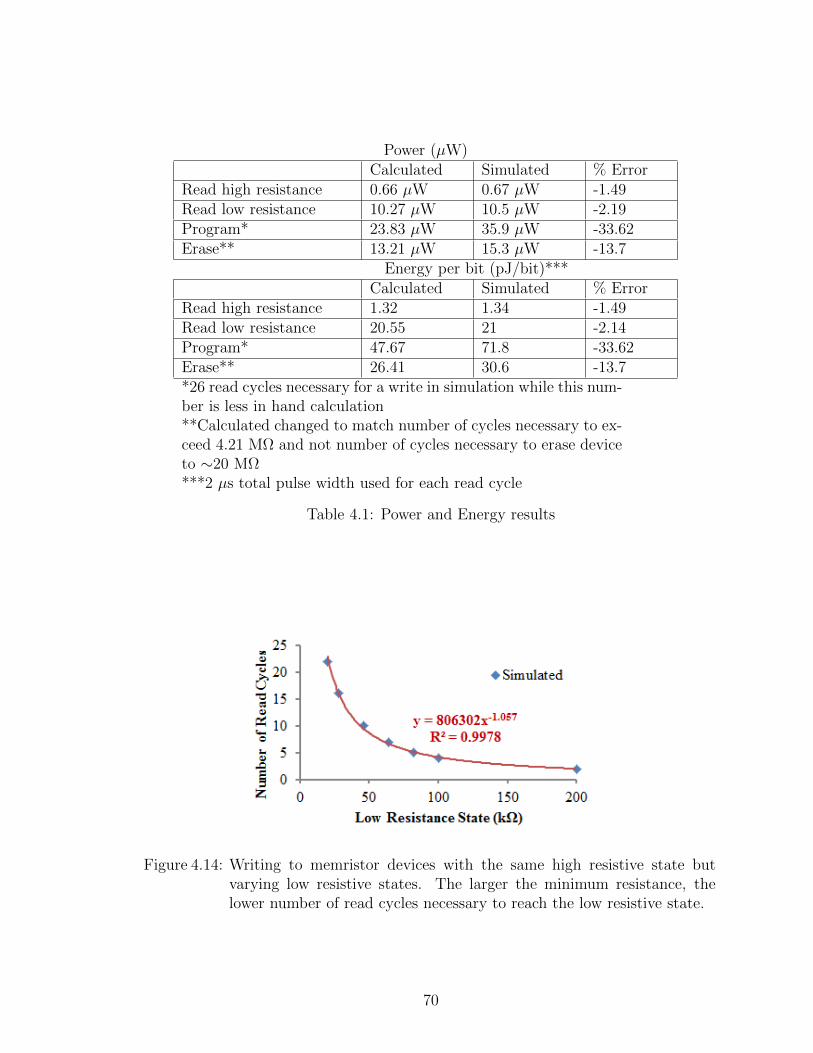
Power (µW)Calculated Simulated % Error
Read high resistance 0.66 µW 0.67 µW -1.49Read low resistance 10.27 µW 10.5 µW -2.19Program* 23.83 µW 35.9 µW -33.62Erase** 13.21 µW 15.3 µW -13.7
Energy per bit (pJ/bit)***Calculated Simulated % Error
Read high resistance 1.32 1.34 -1.49Read low resistance 20.55 21 -2.14Program* 47.67 71.8 -33.62Erase** 26.41 30.6 -13.7*26 read cycles necessary for a write in simulation while this num-ber is less in hand calculation**Calculated changed to match number of cycles necessary to ex-ceed 4.21 MΩ and not number of cycles necessary to erase deviceto ∼20 MΩ***2 µs total pulse width used for each read cycle
Table 4.1: Power and Energy results
Figure 4.14: Writing to memristor devices with the same high resistive state butvarying low resistive states. The larger the minimum resistance, thelower number of read cycles necessary to reach the low resistive state.
70
The adaptive method proposed provides a sensible way to deal with errors (defects)
in the crossbar structure. Errors can be classified in three ways: firstly, the memristor
is in a stuck open state; secondly, the memristor is in a stuck closed state; and thirdly,
the lower-bound or upper-bound resistance targets are not met. In the first two errors
(stuck open or stuck closed), an attempt to write the opposite data to the memristor
will fail. In either case, as long as the memristor is static, the write methodology
will only attempt the write process once. The read process will always produce a
“Logic 1” as defined in the flow diagram in Figure 4.2b. The stuck open or stuck
closed case will not take multiple write cycles in order to determine if the memristor
is functional. To determine if the device works or not, a read in one direction is
performed, an opposite data write is tried (again lasting only one read cycle due to
the static nature of the failed device), and a read verify is performed. If both reads
yield the same result, then the device is non-operational. This method removes the
guesswork from setting hard thresholds and setting maximum write tries before a
memory storage cell is deemed defective.
The defective nature of a stuck open or stuck closed cell is different from a device
that misses the target high and low resistances for memristor devices. These devices
behave in a way that exhibit hysteresis, but they may have larger or smaller ratios
of the resistance in the high state to the resistance in the low state compared to
the design target. Since the proposed method does not deal directly with absolute
resistance values, the exact extremes of the resistance of a certain device is not of
interest. Resistance extremes are dealt with in ratio (Figure 4.14). The larger the
range between the high and low resistive states, the more number of read cycles
necessary to perform a write or erase operation. Also, depending on resistance range,
the pulse widths used for the design may not be enough to distinguish high and low
states. For example, in Figure 4.10, any low level greater than 200 kΩ does not provide
enough separation between the high and low resistive states. The chosen 1 µs pulse
71

widths would already change the device state from one extreme to another during a
read operation. The analyses done in this work examines the memory limitations for
a chosen pulse width, but the values presented can be improved upon with shorter
pulses (< 1 µs) based on improved memristor switching performance.
The advantage of using this method for read/write is to combat the effects of
process variation within the crossbar structure. The exact low level does not matter
except that the level is within operational limits imposed by the 1 µs pulse. The nature
of the low level and high levels of memristive devices to change during operation
requires that the sensing method take this into account. During operation, as long as
the pulses do not change the memristor device to an extreme, then a device that may
have been deemed a failed device under another sensing scheme is salvaged for further
use. This method provides an insightful scheme to combat the effects of resistance
drift as memristors’ absolute extreme resistances change over their lifetime.
The power and energy numbers in Table 4.1 show some disagreement between cal-
culated and simulated values. Eliminating the assumptions made due to the low time
constant values for the different capacitor paths may lead to an agreement. Essen-
tially, the storage capacitors, although their access transistors are in the OFF state,
are leaking and charging depending on the cycle presented by Data. Also, the pe-
ripheral circuitry consumes power not included in the calculated values. Considering
that the same driving circuitry is used to drive the memristor in both its high and
low resistive states, the low current achieved in the high resistive state suggests that
the time constants of the OFF and the ON paths have similar power characteristics,
which account for 0.01 µW. However, in the low resistance state, the OFF and the
ON paths have differing power profiles leading to 0.23 µW disagreement between
simulation and calculation.
The program and erase numbers have a larger error differential because two dif-
ferent models are used to determine the weight change in the memristor. In the
72

calculated case, the weight change is determined through an approximated linear
diffusion model whereby boundary effects are not taken into consideration. In the
simulated model, boundary effects are modeled with a window function, which is why
when the device is in a low resistive state at a boundary, albeit high current, the
memristance does not change as drastically as predicted by the linear model.
The current method proposed takes into account problems that may be more
pronounced in higher-dimension grid, i.e., 4 Kb block size as used in many commercial
flash devices. The resistive nature of the nanowire will be more pronounced for devices
not very close to the driver. This method of determining memory state adjusts to
the resistive drops that may be made when the nanowires are more resistive than
expected. The problem that may affect a larger memory size is excessive voltage
drops which would require tuning the voltage level to accommodate all devices in the
crossbar array. Devices far from the drivers will essentially take longer to write or
erase compared to devices closer to the driver. Essentially, an adaptive read, write,
and erase method allows for a more flexible process technology and will enable the
adoption of the memristor memory sooner since devices that do not meet high and
low resistance criteria may still be used with confidence.
4.5 Chapter Summary
The memristor memory showcased extols the advantages of using the new tech-
nology in memory applications. The method of achieving the read, write, and erase
relate adaptively to each memristor device thereby allowing for increased yield when
it comes to using devices that have differing high to low resistance range. The mem-
ristor memory also exhibits lower power and energy consumption when compared to
flash memory. Unfortunately, the proposed method cannot be directly applied to the
multi-bit memory, since this method depends on writing the memristor to an extreme.
New methods will need to be devised that will allow for reliably writing to the device
73

in the multi-bit case, as well as perform flash-like operations, such as block erasures.
The latter is not necessary, but it would improve the operation per bit statistics when
it comes to power and energy consumption.
74

CHAPTER V
Value Iteration with Memristors
5.1 Introduction
Memristors [20],[93] have been proposed for use in different applications in both
an evolutionary and revolutionary manner with respect to hardware complexity. In
the evolutionary sense, memristors have been proposed for FPGA, cellular neural
networks, digital memory, and programmable analog resistors. From the revolution-
ary perspective, memristors are offered for applications that bring together higher
level algorithms, usually implemented in software, down to the hardware level. These
include proposed architectures such as the hardware that will utilize MoNETA [101],
instar and outstar training [88], optimal control [106], visual cortex [117], etc. The use
of memristors in the evolutionary sense has several limitations [29] due to the nature
of the memristors being used in a Boolean logic computation when direct control of
memristors are very imprecise.
A plausible area to use memristors would be in applications whereby precise re-
sistance values are not required, but the relative values between memristors in the
crossbar are maintained. This approach has been shown successful in simulating a
maze problem [69], but the maze hardware architecture seems harder to fabricate
and realize since memristors are not used in a crossbar configuration. The access
transistors inhibit a crossbar structure, and even if this drawback were ignored, the
75

approach described in [69] requires probing voltages in the memristor network that
may be inaccessible due to spacing requirements for vias and contacts. The work pre-
sented in this chapter seeks to solve the maze problem in using a different approach
that may be realized with current fabrication methods.
The approach whereby precise resistance values on memristors are not required
has been shown successfully through simulation to implement a fuzzy system [57] and
extended to an edge detector learning [58]. Fuzzy systems have multiple applications,
but this paper focuses on ways to bridge the gap between successful algorithms in
artificial intelligence (AI) and memristors. AI algorithms are grounded deeply in
mathematical formulations that breed reproducibility. If memristor crossbars can
implement AI algorithms, then software interface of AI hardware will become less
intricate since hardware will handle more complex computation. This work strives to
link both memristor properties and AI through a basic learning tool, value iteration
through Q-learning [105].
Q-learning is used as an example because of its memory requirement. Q-Learning
learns state-action values (dubbed Q-values) and storing these Q-values in tabular
form for the entire state-action space is shown to reach optimal solutions even under
exploration. The drawback associated with Q-learning stems from the prohibitive
nature of the memory requirement for the tabular form of the algorithm. In order
to circumvent this problem, function approximators have been used to reduce the
memory size required. Function approximators though need careful design because
poor design may lead to divergence.
This chapter is organized as follows: Section 5.2 deals with the mathematical
details concerning Q-learning and an extension of the memristor equations; Section 5.3
introduces the maze application and reconciles Q-learning equation and memristor
equation; Section 5.4 provides simulation results and discussion; and Section 5.5 relays
concluding remarks.
76
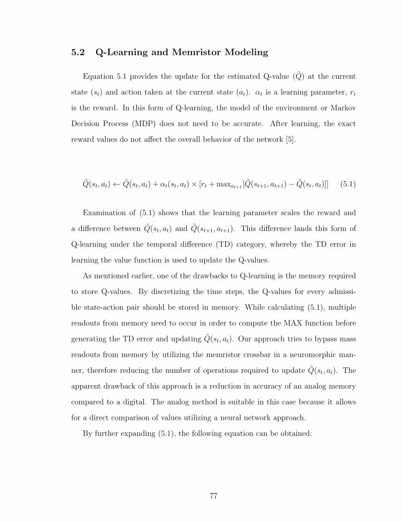
5.2 Q-Learning and Memristor Modeling
Equation 5.1 provides the update for the estimated Q-value (Q) at the current
state (st) and action taken at the current state (at). αt is a learning parameter, rt
is the reward. In this form of Q-learning, the model of the environment or Markov
Decision Process (MDP) does not need to be accurate. After learning, the exact
reward values do not affect the overall behavior of the network [5].
Q(st, at)← Q(st, at) + αt(st, at)× [rt + maxat+1 [Q(st+1, at+1)− Q(st, at)]] (5.1)
Examination of (5.1) shows that the learning parameter scales the reward and
a difference between Q(st, at) and Q(st+1, at+1). This difference lands this form of
Q-learning under the temporal difference (TD) category, whereby the TD error in
learning the value function is used to update the Q-values.
As mentioned earlier, one of the drawbacks to Q-learning is the memory required
to store Q-values. By discretizing the time steps, the Q-values for every admissi-
ble state-action pair should be stored in memory. While calculating (5.1), multiple
readouts from memory need to occur in order to compute the MAX function before
generating the TD error and updating Q(st, at). Our approach tries to bypass mass
readouts from memory by utilizing the memristor crossbar in a neuromorphic man-
ner, therefore reducing the number of operations required to update Q(st, at). The
apparent drawback of this approach is a reduction in accuracy of an analog memory
compared to a digital. The analog method is suitable in this case because it allows
for a direct comparison of values utilizing a neural network approach.
By further expanding (5.1), the following equation can be obtained:
77

Q(st, at)← Q(st, at)(1− αt(st, at)) + αt(st, at)× rt + αt(st, at)×maxat+1Q(st+1, at+1)
(5.2)
The takeaway from (5.2) is that the learning rate places importance on which pa-
rameter is more important by adjusting the contribution of each to the value update.
The MAX function in (5.2) will produce a value, Qmax(st+1, at+1) that can be seen
as a linear combination between Q(st, at) and another value δt thereby giving the
relationship in (5.3).
maxat+1 [Q(st+1, at+1)] = Qmax(st+1, at+1) = Q(st, at) + δt (5.3)
The value of δt can be zero, positive or negative. It is a correcting factor that
discerns how far apart the Q-value of the current state-action pair is from the Q-value
of the next state-action pair. By substituting (5.3) back into (5.2) and eliminating
some terms we obtain (5.4), the final equation describing the targeted value function
updates.
Q(st, at)← Q(st, at) + αt(st, at)× (rt + δt) (5.4)
Neural network inspired approaches have been shown to efficiently perform max-
imizing and minimizing functions [34]. Memristors in the crossbar configuration are
not only used as memory but also as processing elements, i.e., synapses in a neural
network exhibit both functions. By monitoring the current through selected memory
devices, the MAX function can be evaluated in parallel. The next step is to cast (5.4)
in a form that is readily applied to the memristor crossbar, so memristor modeling is
discussed next.
Referring back to total memristance given by (2.11), the flux term φ(t) is the in-
dependent variable and hence the control for the memristor’s resistance. By choosing
78

a constant voltage pulse Vapp and applying this constant pulse for a specified time
tspec, (2.11) can be discretized into n different applications of Vapp for tspec thereby
producing:
MT = R0
√1− β
∑n
Vapp · tspec = R0
√1− β · Vapp · tspec · n (5.5)
where β is defined as (2 · η · δR)/(Q0R20) and n is an integer. The goal in value
iteration is to update the value function, and since we strive to use MT to store the
value function, then the updates to MT will depend on the value of n. The change
between the previous value and the updated value ∆MT can be described by
MT = R0
√1− β · Vapp · tspec · n−R0
√1− β · Vapp · tspec · (n− 1) (5.6)
Furthermore defining a = 1− β · Vapp · tspec · n and b = β · Vapp · tspec, (5.6) can be
rewritten as:
∆MT = R0
√a
(1−
√1 +
b
a
)(5.7)
Since |b/a| < 1, (5.7) can be approximated with the Taylor expansion as:
∆MT∼= R0
√a
[−1
2
(b
a
)+
1
8
(b
a
)2
− 1
16
(b
a
)3
+ ...
](5.8)
For the intended application, Hebbian learning is envisioned. Therefore, if updat-
ing the memristor in one direction, whereby the resistance is always increasing with
increasing n, then the piecewise relationship in (5.9) (keeping two terms of the Taylor
expansion) describes an approximate discretized memristor used in this application.
MT∼=
R0 n = 0
R0 +∑
nR0
√a[−1
2
(ba
)+ 1
8
(ba
)2]n > 0
(5.9)
79

The next section will explain the maze application in detail, thereby reconciling
the derived memristor behavior in (5.9) and the value iteration equation in (5.4).
5.3 Maze Search Application
5.3.1 Introduction
Given a test maze (Figure 5.1) we would like to train through value iteration,
the generation of optimal actions to reach the target (RED) from the start position
(GREEN). The 16×16 maze shows admissible states in white and inadmissible states
in black. Our approach to solving this maze using memristors is to store the value of
each state (admissible or inadmissible) in a memristor crossbar. A 16×16 memristor
crossbar array is therefore needed to store all values. The maze pattern can be
preprogrammed to the crossbar array whereby inadmissible states are programmed to
ROFF and the admissible states are programmed to values around an initial resistance
R0. The search space is discretized into time periods where one move is made per
unit time. Each move made must either progress to adjacent states or stay at the
current state. For example, if at time period p=1 and the current state is the green
square, then the three valid states for transition are the two adjacent white squares
and the green square.
Decisions regarding state transition are made by obtaining the stored values of
valid states in reference to the present state. The drawback to this one-step lookahead
approach is its limited depth search that takes longer for training to converge to an
approximation of the optimal path from start to end. The advantage of this approach
is a less complex hardware implementation when using the crossbar.
80

Figure 5.1: Maze example showing starting position (green square) and ending posi-tion (red square)
5.3.2 Hardware Architecture
The memristor crossbar is used to store state values. To reduce hardware com-
plexity with respect to accessing the crossbar, two crossbars are used whereby one
stores the values in order (Network 1 in Figure 5.2) as prescribed by the state order
in Figure 5.1, while the other crossbar stores values of Figure 5.1 mirrored about
the diagonal from the top left corner to the bottom right corner (Network 2 in Fig-
ure 5.2). The top level system in Figure 5.2 shows an agent acting on the environment
(the maze). The components of the system are: controller, memristor network, com-
parators (C blocks), and actor. The actor performs chosen actions, the comparators
compare two values within the memristor crossbar, the memristor network performs
the MAX function and generates next state information, and the controller coordi-
nates communication between all components. The two memristor networks have the
81

Figure 5.2: (a) Top Level system showing information flow (b) Network schematicshowing analog and digital components
82

same components and a detailed network schematic is also provided in Figure 5.2.
The network blocks have two sets of neurons. Each set contains 16 neurons,
allowing access to the value of each state on the memristor crossbar array. This
architecture is chosen to approximate a recurrent neural network. Network 1 may
be viewed as the forward path and Network 2 may be viewed as the feedback path.
Neurons correspond to horizontal and vertical coordinates in Figure 5.1. At any given
time the admissible actions are: stay at current state, move one space in any diagonal
direction, any horizontal direction, or any vertical direction. Network 1 determines
the next Y position, while Network 2 determines the next X position. The controller
coordinates the actions of the networks using four control phases: Start, Run, Check,
and Train.
That Start phase is a wait phase whereby the crossbar network is not accessed. All
the switches in Figure 5.2 are open, all input and output neurons disabled, and output
registers are zeros. In the Run phase, the network obtains the next position; the first
neuron to spike will have its corresponding output register latch a “1” while the others
are “0,” and will provide a signal to the controller that this phase is complete. In
the Check phase, the digital network asserts VREAD and connects RLOAD to decipher
the values stored at two locations (the value of current state vs. that of the next
state). If the current state’s value is greater than or equal to the next state’s then
a punish signal is generated. In the Train phase, the punish signal is used to reduce
the weight of the current state. The neural network is used to translate the time to
spike to approximate the environment. The architecture is a hybrid architecture that
combines both analog processing with digital controls. The next section makes a case
as to why this architecture is suitable for value iteration and the maze problem.
83
5.3.3 Hardware Connection to Q-Learning
For the maze application, value iteration updates based on (5.4), but the exact
nature of the update term, αt(st, at)× (rt + δt), has not clearly been defined. In the
maze problem, αt(st, at) will be limited to take on a value of either –1 or 0, and the sum
of rt and δt can be cast to take on the value of ∆MT in (5.8), R0
√a[−1
2
(ba
)+ 1
8
(ba
)2].
This proposed matching works in this application because the envisioned system has
memristors initialized around R0 and any memristor updates will adjust resistance
by ∆MT . αt(st, at) is –1 if Q(st, at) is greater than or equal to Qmax(st+1, at+1),
otherwise αt(st, at) is 0. The punish signal generated in the Check phase determines
which value αt(st, at) takes. This restriction on αt(st, at) ensures Q(st, at) is always
decreased when updated since rt + δt is always a positive number.
The value for αt(st, at) depends on Qmax(st+1, at+1), and Qmax(st+1, at+1) is ob-
tained from the neuromorphic side of the circuit. A simple leaky integrate and fire
neuron should work for this purpose. The schematic in Figure 5.3a is used to explain
the nearest neighbor concept. From a current X position and a current Y position,
switch corresponding to Xj is activated and Yi−1, Yi, and Yi+1 are enabled. Using
RC integrators to model neuron internal state, the equivalent circuit for these ac-
tivated devices is shown in Figure 5.3b. The first order RC circuit shows that the
internal state of the neurons take on the form vn(1− e−t/(MijCint)
). By choosing a
spiking threshold vthresh for the neurons less than vn, neuron j can spike whenever
vn(1− e−t/(MijCint)
)reaches vthresh. The difference between the activated neurons lies
in tjspike, how long it takes for neuron j to spike:
tjspike > −Mij · Cint · ln(
1− vthreshvn
)(5.10)
According to (5.10), each memristor allows each neuron to spike at a different
time. If three memristors were chosen, then the memristor with the lowest value will
84

Figure 5.3: (a) Activation of neurons (b) Equivalent circuit of activated devices
cause its neuron to spike sooner than the other memristors, thereby guaranteeing the
highest conductance memristor will be chosen when trying to determine the MAX
function. This disparity in charging activated neurons’ internal state capacitors is
therefore used to determine Qmax(st+1, at+1).
5.4 Results and Discussion
MATLAB simulations were performed on the derived models. The parameters
used to evaluate performance are: vthresh/vn=0.75, Vapp=1.2 V, Cint=1 pF, tspec=2 ms,
β= -199.8 V−1·s−1, R0=2 MΩ, RON=20 kΩ, and ROFF=20 MΩ. Figure 5.4a com-
pares the effect of keeping more terms of the Taylor expansion in (5.8), showing that
preserving at least two terms provides enough accuracy for the current modeling.
When two terms are kept, the error quickly reduces to less than one percent at n =3.
Figure 5.4b shows the graph of (5.10) and how the choice of vthresh can affect
circuit operation. Since the MAX function depends on the comparison of spike times
of different neurons, separation of these spike times for different n values is critical
for correct circuit operation. By increasing vthresh, while other parameters are kept
85

Figure 5.4: (a) Number of terms vs. the percent error (b) Effect of vthresh on thecharging time to spike (c) Number of steps before convergence using thebaseline value function (d) Number of steps before convergence usingmemristors
86

Figure 5.5: (a) Optimal path using the baseline value function (b) Near optimal pathusing the memristor crossbar (suboptimal moves circled)
at their previous levels, there is a wider change in spike time. The quoted times
are in µs, and if transistors used for implementation are sensitive to the hundreds
of nanosecond range, then there should be minimal problem detecting the larger of
n=50 and n=51.
Figure 5.4d shows the relationship between the number of steps to reaching target
and the number of training stages for convergence. The outlined process in this
paper prefers exploration in the first iteration. During the second iteration, the
number of steps is drastically reduced. To show that learning converges, after 26
iterations, the network stops updating since αt(st, at) does not reach the value of –1
due to the stable path chosen by the neural network. The results in Figure 5.4d
are juxtaposed with that in Figure 5.4c using conventional methods where Q(st, at)
is updated using the relationship in (5.1) with αt(st, at)=0.2. This value function
is dubbed the baseline value function and is used as a point of comparison. The
results show that conventional method converges to one of the optimal paths, taking
much more effort with designing the value function to limit the number of steps to
convergence.
87

Figure 5.5 shows two solutions: Figure 5.5a shows the path obtained through the
baseline value function while Figure 5.5b shows results using the memristor modeled
network. The first path is an optimal path, while the second is near-optimal. The
discrepancy between the two lies in the current method being inefficient at diago-
nal moves. All the sub-optimal moves made in the memristor implementation were
due to making a vertical and a horizontal move instead of one diagonal move. The
discrepancy is due to the 2-step process in obtaining the next state location.
5.5 Chapter Conclusion
We have shown the concept of value iteration being applied to the memristor
crossbar in a way that is realizable with the aid of CMOS hardware. We have shown
how maze learning can be implemented using the crossbar. We have dissected the
memristor modeling equation to show that the neural network model whereby state
information can be translated to delayed spike timing is shown. The goal behind this
work was the mapping of a higher level algorithm to the memristor crossbar, and the
simulation results in the chapter have proven this is possible.
88
CHAPTER VI
Closing Remarks and Future Work
6.1 Chapter Conclusions
Memristors have been proposed for multiple applications, as reviewed in Sec-
tion 1.2 and including the memory repair application in Appendix A. These applica-
tions have different requirements stemming from the need to either use memristors as
discrete elements or in a crossbar structure. Each device implementation brings about
challenges as well as advantages. The challenge with the discrete element memristor
lies in the processing of such devices, in order to take advantage of the promised
density gains. The crossbar structure is simpler to fabricate but runs into leakage
problems and low device yield. There is a need for reliable ways of using the mem-
ristor, i.e., training the memristor to take on appropriate values. This thesis strived
to explore multiple avenues of training the memristor crossbar in order to adhere to
the promises of the high density memory/processing element structure.
Chapter III dealt with reliably training a memristor using STDP. The work in
this chapter promoted the view that specific resistance value training is not necessary
and is most likely ideal when dealing with memristors. Realization of a WTA system
using STDP learning and memristors was shown to consume less area due to a novel
design technique of estimating the STDP curve and using the memristor properties to
realize the exponential relationship. Incorporating memristors simplified the circuit
89

design, which enabled a digital design in order to use less components on chip. In
addition to less components on chip, the power consumption during the evaluation
phase is much lower with the memristor design than with the CMOS design. The
chosen method to train memristors to realize STDP showed memristors can be used
reliably and that memristor design can surpass the current implementations of STDP
which rely on analog circuit design using large capacitors.
Chapter IV strived to utilize the advantage of the crossbar structure, since the
architecture in Chapter III was not suitable for the crossbar. The example in Chap-
ter IV is that of a digital memory and how to both program and erase this memory.
The crossbar structure is modified to include diodes for isolation, as proposed in liter-
ature. The diode isolation allows a higher noise margin, thereby aiding in decoupling
neighboring memristors. By combining the memristor and the diode, a novel adaptive
scheme was used to program the memristor crossbar memory to different logic states.
Also, the memristor memory is shown to have benefits related to reading and writing
energy when compared to flash memory. Lastly, this training scheme for memristors
relies on using each device as its own reference, thereby potentially improving the
yield of a crossbar memory.
Chapter V presents a method of training the memristor crossbar using a reinforce-
ment learning approach. This approach showed that with a simple digital controller,
the memristor crossbar could be used to self-assemble an environmental model that
can be used to solve a maze problem. The link between Q-Learning and the proposed
memristor crossbar training hardware was established. Using the current training
scheme, a four instruction processor would be able to demonstrate value iteration.
Therefore, the memristor crossbar with analog memristors possesses the ability to
reduce hardware complexity.
The main contributions of this thesis lie in setting up building blocks and method-
ologies for training memristors utilized in either a discrete manner or a crossbar
90
manner. Memristors show promise because their proposed application space spans
bio-inspired computation on chip to massively dense digital memory. At this stage,
applications should drive innovative use of memristors from the architectural perspec-
tive, while process technologists more vividly understand device properties, transport
mechanisms, and causes for defects. This view influences the future work, which
should deal mostly in more training methods, building blocks, and confirmation of a
CMOS-memristor hardware that combines the knowledge gathered in cross-disciplines
(Artificial intelligence, Neuroscience, and Electrical Engineering).
6.2 Future Work
A strong, useful prototype in the future will be most beneficial to this line of
research. With respect to memristor memory, methods of reliably integrating mem-
ristors with CMOS and demonstrating different memory operations is key. Multiple
read, program, and erase methodologies for memristors and resistive memory devices
are present in literature. Extending the proposed adaptive method to a memristor
and striving to use such method to improve memory yield in lab on a 10×10 memris-
tor crossbar memory would be a viable effort in extending the value of the memristor
technology. Digital memory is mature enough to be at the vanguard when CMOS in-
tegration is concerned because the integration efforts will provide very new questions
to ponder. These questions may need to be answered in order to realize any other
application that possesses lower noise margin compared the digital memory design.
By achieving success in the digital memory, the next step is to apply such knowl-
edge to the development of neuromorphic circuitry. The real value of the memristor
lies in its ability to not only serve as storage units, but also processing elements. With
respect to the neuromorphic approach, the next phase is to successfully implement a
large scale control or inferencing application. The control application may be that of
motor control. The motor control hardware should be adaptable to a varying range
91

of control problems. Adaptable hardware is envisioned with the properties of the
memristor, hence an adaptive-critic design approach is considered for motor control,
for existing adaptive-critic designs have been shown to be very effective in designing
systems that learn and adapt in real time [31]. The difficulty to realizing these mem-
ristive adaptive hardware lies in the uncertainty and imprecise control of memristors,
so the lessons learned in realizing a digital memory in crossbar structure will further
aid the realization of an adaptive hardware. Best practices of crossbar training and
better model development will aid in alleviating the problem of imprecise memristor
training.
The adaptive-critic design will have a CMOS/memristor circuit block that will be
trained to represent the actor (control law), and another CMOS/memristor circuit
block will be trained to represent the critic (behavioral goals). The overall system
behavior will depend on the spike training of these two networks to acquire the de-
sired outcome of the control system. Introducing memristors in optimal control will
strive to leverage the zero-static power consumption of memristor synapses and low
power operation of analog very-large-scale-integration (VLSI) technology. The hard-
ware used for the reinforcement learning problem can be a starting point to realizing
this adaptive-critic design. The steps involved would be to: (1)Modify architecture
for multiple algorithms, e.g., ε−greedy exploration, not just the greedy algorithm
espoused in Chapter V; (2)Circuit redesign of the proposed hardware to account
for bidirectional neurons; (3)Since combining with CMOS and possibly the micro-
processor, multiplexing methods for specified bus widths of the processor should be
investigated. These aforementioned steps will be intermediaries to achieving hardware
for algorithms that require higher level abstraction like the optimal control problem.
92

APPENDIX
93

APPENDIX A
Memory Yield Enhancement with Memristor
Built-in Self-Repair Circuit
Digital memory is the most promising approach with respect to a commercial
product, which is why extensive research in this area has resulted in hundreds of
patents as well as an impressive list of problems that may be encountered in a mem-
ristor crossbar memory. In the era of memristor memories, the memory designer will
need to provide ways of dealing with defective memory cells. Due to aggressive scal-
ing into the nanometer regime and devices only a few tens of nanometers thick, the
number of defective memory cells will dramatically increase, thereby forcing newer
methods that will handle larger fault pattern densities.
Due to the binary nature of memory cells, a faulty memory cell is unusable;
therefore, a workaround the faulty cell is needed in order to salvage the memory chip.
With every memory chip, redundant memory cells are incorporated to anticipate
any errors, and reconfigurable techniques are used to replace rows and/or columns
that contain faulty cells with the redundant rows/columns. This appendix explores
the use of the nonlinear analog memristor model in a Built-in Self-Repair (BISR)
architecture that is appropriate for embedded memories. The next section provides a
94

brief description of the architecture and some earlier work that leads to the proposed
system and results from the memristor circuitry.
A.1 Architecture Description and Results
Given a memory array consists of m by n memory cells for data storage, most
memory have extra rows and/or columns in case there exists faulty cells in the m by
n memory array. In the memory model, assume there exists p extra rows and q extra
columns to replace rows and columns with faulty cells. As long as the number of rows
to be replaced is less than p, and the number of columns to be replaced is less than
q, then the memory is repairable. The goal of the repair architecture is to minimize
an energy function and find near optimal repair scheme. An example of a 4x4 fault
pattern repair architecture is shown in Figure A.1.
Memristors are used in the architecture to store transposed fault patterns as de-
scribed in [52]. The BISR circuitry operates in the context of a memory system,
whereby a BIST memory tests a large memory array and creates a compressed defect
pattern as shown in Figure A.2. The defect pattern is then transferred to the BISR
quadrants as shown.
The power circuitry with the Set and Reset signals is used to write and erase the
fault pattern from the memristors. The muxes allow the change of operations between
a run operation, a write operation, and an erase operation. In both the write and
erase operations, RX and WLX are asserted and the corresponding access transistors
provide access to the memristors of interest. Examples of these operations are shown
in Figure A.3.
Splitting up the architecture into four quadrants, the top left (quadrant 2) and
the bottom right (quadrant 4) are static, and their current draw is dependent on the
sizing of these unchanging transistors. The top right and the bottom left quadrants
(quadrants 1 and 3, respectively), on the other hand, will draw different amounts of
95

Figure A.1: BISR example circuitry for a 4x4 fault pattern
Figure A.2: Example of programming a BISR memory pattern. The memory array istested for faults (dots mean faulty cells), and compressed defect patternis generated, and this pattern is written to the BISR memory quadrants
96

current depending on the resistance registered by the memristors. From Figure A.3,
we can see that these quadrants will store transposed state of the fault pattern based
on the defined control switches.
The bias generators provide initial bias to the row and column neurons. Neurons
are represented as triangles in Figure A.1, and they are implemented with specially
designed threshold buffers whereby their stable output values are either a Logic “1”
or Logic “0.” In the run operation, all neurons inhibit one another, and depending
on the fault pattern stored in the top right and bottom left quadrants, some neu-
rons are inhibited more than others. This causes an equilibrium to be reached at
a certain point, whereby the neurons still operational signal that their correspond-
ing rows/columns should be replaced with spare rows/columns. Neuron excitation
is achieved through the bias generators, and neuron inhibition is achieved through
the currents drawn from the ON transistor paths in Figure A.1. Current addition
and subtraction is converted to voltage and then to Boolean form using the buffer
mentioned earlier.
The BISR circuitry shown relies on a built-in self-testing (BIST) circuit that
will provide the compressed defect pattern to be programmed to the BISR array of
Figure A.1. The BIST will also determine how each neuron in the BISR will be
biased. The neurons in the BISR circuitry will receive different biases based on the
number of defective elements present in each vertical line the neurons are driving.
With the BISR circuit architecture explained, the remaining task left is to provide a
theoretical background for its conception.
Solving optimization problems with neural networks was explored by Hopfield for
the Traveling Salesman Problem [34]. Hopfield used a recurrent neural network with
the Lyapunov energy for the neural network as the objective function for optimiza-
tion. The neural network approach, in fact, reduced the complexity of finding local
minimums compared to using other approaches. The architecture shown in Figure A.1
97

is a recurrent neural network similar to Hopfield’s network, but the problem solved
is that of the memory repair problem.
The energy function for Hopfield’s neural network is given by (A.1):
ENN = −1
2
∑i
∑j
wijsisj −∑i
sibi (A.1)
where ENN is the neural network energy, wij is the synaptic weight between neuron
i and neuron j, si is the current state of neuron i, sj is the current state of neuron
j, and bi terms are the input biases for each of the neurons. The sj terms take on
binary values of either 1 or 0, depending on whether the neuron is in a firing state or
not. In the context of the memory repair problem, if a neuron is in a firing state, then
the neuron signals that a certain row or column needs to be replaced. The neural
network in effect seeks to minimize (A.1) due to the current network configuration.
From the energy function description, the first step of the memory repair problem
is to cast the objective function in the same form as (A.1). The memory repair cost
function is dealt with at length in [52], with a resultant cost function modeled as
(A.2a) and (A.2b).
C1 =A
2
[(m∑i=1
si
)− p
]2+A
2
[(n∑i=1
sm+i
)− q
]2(A.2a)
C2 = B
[m∑i=1
n∑j=1
dij(1− si)(1− sm+j)
](A.2b)
C1 is the cost function associated with the number of covered rows and columns.
This cost function grows quadratically if the number of rows or columns to be cov-
ered exceeds p or q, respectively. C2 is the cost function associated with unrepaired
defective cells, where dij is takes on the value of 1 if a cell is defective and takes on the
value of 0 otherwise. The total cost to be minimized in the memory repair problem
98

Figure A.3: (a) Erasing the fault pattern from the BISR array (b) Programming aspecific fault pattern to the BISR array
99

is the addition of both of these cost functions. By adding these cost functions and
comparing to (A.1), the matched terms produce the relationships that help set the
biases in the “Programmable Row Neuron Bias Generators” in Figure A.1, the sizing
of the quadrants 2 and 4 transistors, and the current defect pattern to be written to
quadrants 1 and 3. For more details on the expressions, we refer the reader to [52].
The next subsection deals with the simulation results performed on a host of different
schemes with different number of neurons.
A.2 Results and Discussion
The goal of the current experiments was to see if the BISR architecture developed
for purely CMOS neural network is able to be ported well to the memristor array.
The process of writing to the array as shown in Figure A.3 involves turning off the
neural pathway and allowing the bias drivers to directly access the memristors for
programming or erasing selected devices. An assumed behavior in this scheme is that
multiple devices can be programmed or erased at the same time. Our simulation
results show that multiple memristors can be driven to one extreme or another using
the current scheme. The memristors reach their terminal resistances at different
times using this scheme since their starting resistances may be about 1% different.
The programming and erasing schemes use a higher voltage (±2 V) to change the
resistance of the memristor. The neurons, on the other hand, use a lower voltage
(1.2 V) during operation. The BISR architecture was simulated with transistors in
the IBM 130 nm technology. The memristor model used is the nonlinear dopant drift
model derived using (2.8) and (2.9).
The first study performed is to derive the transient behavior of the BISR circuitry.
Figure A.4 and Figure A.5 show simulation results for compressed 4x4 defect patterns.
In the pattern, a value of “1” signifies a faulty cell while that of “0” signifies a normal
operating cell. Since the current repair scheme replaces rows and columns, the goal
100

for the circuitry is to cover all faulty cells with a total of four rows and columns
(2 each). The architecture in Figure A.1 has 8 neurons with four neurons’ outputs
corresponding to the status of replacing rows and the other four neurons’ outputs
corresponding to the status of replacing columns. The waveforms in Figure A.4 and
Figure A.5 represent the eight neuron outputs with indices labeled as Row0 through
Row3 and Col0 through Col3.
All the neuron outputs start rising when all the neurons activated at once. Fig-
ure A.4 shows that Col2 is selected first because this signal is the first to reach 1.2 V;
Row2, Col0, and Col3 are greatly inhibited, so they all fall to 0 V very quickly after
activation. After Col2 is selected, the other falling signals begin to compete once
again, and Col1 wins out and reverses its direction to end up at 1.2 V. At this point,
Row0, Row1, and Row3 are still in contention for selection. After the selection of
Col2, Row0 and Row3 reverse their direction and become selected while Row1 falls
to 0 V. At this point all the faults are covered by the selected rows, and the logic
values for the neuron outputs can be clocked in by the “Row Neuron Output Shift
Register” and the “Column Neuron Output Shift Register” in Figure A.1.
Figure A.5 is shown as a second example to present the case that the transient
behavior really depends on the fault pattern programmed in the compressed fault
memory. Figure A.4 neuron outputs settled to 1.2 V one after another except for
Row0 and Row3, but the pattern in Figure A.5 forces the circuitry to make decisions
two at a time. First, Row1 and Col3 settle to 1.2 V, then afterward Row3 and
Col0 win out to settle at 1.2 V, while Row0 and Col2 drop to 0 V. The patterns in
Figure A.4 and Figure A.5 were chosen carefully to see whether the neural network
will be effective in balancing spare resources.
For every memory, there are a limited number of spare rows and columns, and
by selecting a spare column for repair, there exists one less number of spare columns
to be used for repair. In Figure A.4, the spare columns were used up first before
101

Figure A.4: Fault pattern and transient simulation results showing the selected neu-ron coverage scheme for the fault pattern shown
the spare rows were considered. This problem would not have been solved correctly
if the neural network came out with the solution Col0, Col1, Col2, and Col3. By
choosing two column solutions in the first two tries, the network limited itself to
cover the rest of the faults with spare rows. On the other hand, Figure A.5 shows a
different behavior where the neural network picks Row1 and Col3 and then Row3 and
Col0. The existence of this behavior hints that with proper design, an appropriate
balancing of spare row and column selection can be tuned with the neural network so
in a larger fault pattern array, too many spare rows are not used up before columns
or vice versa. This result satisfies the minimum cost constraint modeled in (A.2a).
Since memristor integration with CMOS is still at a low yield stage, the current
design, where faulty patterns are written to the compressed defect memory, may have
problems. For example, the memristors could behave in a non-programmable way,
where they are either in a stuck-open state or a stuck-short case. With these def-
initions of defective, the effect of defective memristors was studied using the fault
pattern in Figure A.4a. When one memristor is in a stuck state, the neural network
performs correctly with 100% of faulty memory cells repaired. This relationship oc-
curs even when three memristors are in a stuck state (∼9% memristors are defective).
102

Figure A.5: Fault pattern and transient simulation results showing the selected neu-ron coverage solution for the fault pattern shown
The failure to cover all faulty memory cells occurs when defective memristors are in
coupled configuration. This means that the corresponding defective memory cell in-
formation stored in both quadrants 1 and 3 are defective. This coupling essentially
rewrites the defect pattern of the compressed memory allowing the neural network
to believe there is no faulty memory cell when in fact there is. A much deeper study
needs to be performed in a larger array, whereby the defects in quadrants 1 and 3 are
coupled.
For the small array presented, the non-coupling memristor defects do not affect the
result of the BISR circuitry, but the defects of the neuron greatly affect the behavior.
The neuron can have multiple defects: incorrect biasing, stuck in a firing state (Logic
“1”), and stuck in a non-firing state (Logic “0”). In the 4x4 defect pattern array
of Figure A.4, when one neuron is in a stuck state, the repair success is lowered
to 62.5% while two neurons defective lowers this value further down to 8.6%. This
method shows that the neurons should be deemed fairly fault free in order to get
proper behavior.
The neuron fault results do not have a dampening effect on the BISR circuitry
because this method should be used with a larger defect pattern - 10×10 or more.
Neural network robustness grows as the size of the network grows. A study done on
103

the array size with respect to number of neuron failures is presented in [52]. The
effect of neuron failures degrades the repair scheme more gracefully when there are 40
neurons as opposed to 20 neurons. One neuron fault still rendered the scheme ∼95%
successful in the 40 neuron case and ∼85% in the 20 neuron case. In next generation
memory repair schemes, the yield problems will mostly lie in the memristors and not
so much on the CMOS circuitry if the transistors sizes are made large enough.
A.3 BISR Conclusion
A BISR circuitry is converted from CMOS only technology to that utilizing mem-
ristors. The BISR circuitry is shown to solve the memory repair optimization problem
quite well. For a 4×4 array, the defect pattern is shown to determine the behavior
of the neural network, thereby proving that the network will settle to its lowest en-
ergy state. The network is also shown to exhibit a balancing technique, where equal
numbers of rows and columns are used for the repair scheme. The BISR circuitry is
shown to be resistant to minor defects in the memristor memory, but very susceptible
to defective neurons.
104

BIBLIOGRAPHY
105

BIBLIOGRAPHY
[1] Afifi, A., A. Ayatollahi, and F. Raissi (2009), Implementation of biologi-cally plausible spiking neural network models on the memristor crossbar-basedcmos/nano circuits, in European Conference on Circuit Theory and Design,ECCTD ’09, IEEE, New York, doi:10.1109/ECCTD.2009.5275035.
[2] Akinaga, H., and H. Shima (2010), Resistive random access memory (reram)based on metal oxides, Proceedings of the IEEE, 98 (12), 2237 –2251, doi:10.1109/JPROC.2010.2070830.
[3] Ananthanarayanan, R., S. K. Esser, H. D. Simon, and D. S. Modha (2009),The cat is out of the bag: cortical simulations with 109 neurons, 1013 synapses,in Proceedings of the Conference on High Performance Computing Networking,Storage and Analysis, SC ’09, pp. 63:1–63:12, ACM, New York, NY, USA, doi:http://doi.acm.org.proxy.lib.umich.edu/10.1145/1654059.1654124.
[4] Annunziata, R., P. Zuliani, M. Borghi, G. De Sandre, L. Scotti, C. Prelini,M. Tosi, I. Tortorelli, and F. Pellizzer (2009), Phase change memory technol-ogy for embedded non volatile memory applications for 90nm and beyond, inElectron Devices Meeting (IEDM), 2009 IEEE International, pp. 1 –4, doi:10.1109/IEDM.2009.5424413.
[5] Balleine, B., N. Daw, and J. ODoherty (2009), Multiple forms of value learningand the function of dopamine, in Neuroeconomics: decision making and thebrain, edited by P. W. Glimcher, pp. 367–385, Academic Press.
[6] Bao, B., Z. Liu, and J. Xu (2010), Steady periodic memristor oscillatorwith transient chaotic behaviours, Electronics Letters, 46 (3), 237 –238, doi:10.1049/el.2010.3114.
[7] Beck, A., J. G. Bednorz, C. Gerber, C. Rossel, and D. Widmer (2000), Repro-ducible switching effect in thin oxide films for memory applications, AppliedPhysics Letters, 77 (1), 139–141.
[8] Bickerstaff, K., and E. Swartzlander (2010), Memristor-based arithmetic,in Signals, Systems and Computers (ASILOMAR), 2010 Conference Recordof the Forty Fourth Asilomar Conference on, pp. 1173 –1177, doi:10.1109/ACSSC.2010.5757715.
106
[9] Biolek, Z., D. Biolek, and V. Biolkova (2009), Spice model of memristor withnonlinear dopant drift, Radioengineering, 18 (2), 210–214.
[10] Blakemore, C., and E. A. Tobin (1972), Lateral inhibition between orientationdetectors in the cat’s visual cortex, Experimental Brain Research, 15 (4), 439–440, 10.1007/BF00234129.
[11] Bofill-i Petit, A., and A. F. Murray (2004), Synchrony detection and amplifica-tion by silicon neurons with stdp synapses, Neural Networks, IEEE Transactionson, 15 (5), 1296–1304.
[12] Borghetti, J., Z. Y. Li, J. Straznicky, X. M. Li, D. A. A. Ohlberg, W. Wu,D. R. Stewart, and R. S. Williams (2009), A hybrid nanomemristor/transistorlogic circuit capable of self-programming, Proceedings of the National Academyof Sciences of the United States of America, 106 (6), 1699–1703.
[13] Burr, G. W., B. N. Kurdi, J. C. Scott, C. H. Lam, K. Gopalakrishnan, andR. S. Shenoy (2008), Overview of candidate device technologies for storage-class memory, IBM Journal of Research and Development, 52 (4.5), 449–464.
[14] Cassenaer, S., and G. Laurent (2007), Hebbian stdp in mushroom bodiesfacilitates the synchronous flow of olfactory information in locusts, Nature,448 (7154), 709–713.
[15] Cauwenberghs, G. (1998), Neuromorphic learning vlsi systems: A survey, inNeuromorphic Systems Engineering, The Kluwer International Series in Engi-neering and Computer Science, vol. 447, edited by T. S. Lande, pp. 381–408,Springer US.
[16] Chen, E., et al. (2010), Advances and future prospects of spin-transfer torquerandom access memory, Magnetics, IEEE Transactions on, 46 (6), 1873 –1878,doi:10.1109/TMAG.2010.2042041.
[17] Choi, J., and B. Sheu (1993), A high-precision vlsi winner-take-all circuit forself-organizing neural networks, Solid-State Circuits, IEEE Journal of, 28 (5),576 –584, doi:10.1109/4.229397.
[18] Choi, S.-J., et al. (2011), Synaptic behaviors of a single metal-oxide-metal re-sistive device, Applied Physics A: Materials Science and Processing, 102 (4),1019–1025.
[19] Chua, L., and S. M. Kang (1976), Memristive devices and systems, Proceedingsof the IEEE, 64 (2), 209 – 223, doi:10.1109/PROC.1976.10092.
[20] Chua, L. O. (1971), Memristor - missing circuit element, IEEE Transactions onCircuit Theory, CT18 (5), 507–519.
107

[21] Cong, J., and B. Xiao (2011), mrfpga: A novel fpga architec-ture with memristor-based reconfiguration, in Nanoscale Architectures(NANOARCH), 2011 IEEE/ACM International Symposium on, pp. 1 –8, doi:10.1109/NANOARCH.2011.5941476.
[22] Csaba, G., and P. Lugli (2009), Read-out design rules for molecular crossbararchitectures, Nanotechnology, IEEE Transactions on, 8 (3), 369–374.
[23] Cutsuridis, V., S. Cobb, and B. P. Graham (2008), A ca2 + dynamics modelof the stdp symmetry-to-asymmetry transition in the ca1 pyramidal cell of thehippocampus, in Proceedings of the 18th international conference on ArtificialNeural Networks, Part II, ICANN ’08, pp. 627–635, Springer-Verlag, Berlin,Heidelberg.
[24] Dan, Y., and M.-m. Poo (2004), Spike timing-dependent plasticity of neuralcircuits, Neuron, 44 (1), 23–30, doi: DOI: 10.1016/j.neuron.2004.09.007.
[25] Driscoll, T., Y. Pershin, D. Basov, and M. Di Ventra (2011), Chaotic mem-ristor, Applied Physics A: Materials Science and Processing, 102 (4), 885–889,10.1007/s00339-011-6318-z.
[26] Ebong, I., and P. Mazumder (2010), Memristor based stdp learning network forposition detection, in Microelectronics (ICM), 2010 International Conferenceon, pp. 292 –295, doi:10.1109/ICM.2010.5696142.
[27] Ebong, I., and P. Mazumder (2012), Cmos and memristor-based neural networkdesign for position detection, Proceedings of the IEEE, 100 (6), 2050 –2060, doi:10.1109/JPROC.2011.2173089.
[28] Ebong, I., D. Deshpande, Y. Yilmaz, and P. Mazumder (2011), Multi-purposeneuro-architecture with memristors, in Nanotechnology (IEEE-NANO), 201111th IEEE Conference on, pp. 431 –435, doi:10.1109/NANO.2011.6144522.
[29] Ebong, I. E., and P. Mazumder (2011), Self-controlled writing and erasing ina memristor crossbar memory, Nanotechnology, IEEE Transactions on, 10 (6),1454–1463.
[30] Eshraghian, K., K.-R. Cho, O. Kavehei, S.-K. Kang, D. Abbott, and S.-M. S.Kang (2011), Memristor mos content addressable memory (mcam): Hybridarchitecture for future high performance search engines, Very Large Scale In-tegration (VLSI) Systems, IEEE Transactions on, 19 (8), 1407 –1417, doi:10.1109/TVLSI.2010.2049867.
[31] Ferrari, S., and R. F. Stengel (2004), Online adaptive critic flight control, Jour-nal of Guidance Control and Dynamics, 27 (5), 777–786.
[32] Grupp, L. M., A. M. Caulfield, J. Coburn, E. Yaakobi, S. Swanson, P. Siegel,and J. Wolf (2009), Characterizing flash memory: Anomalies, observations, and
108

applications, in Proceedings of the 42nd International Symposium on Microar-chitecture, pp. 24–33.
[33] Ho, Y., G. M. Huang, and P. Li (2009), Nonvolatile memristor memory: devicecharacteristics and design implications, in IEEE/ACM International Confer-ence on Computer-Aided Design-Digest of Technical Papers, ICCAD 2009, pp.485–490, IEEE.
[34] Hopfield, J. J., and D. W. Tank (1985), “neural” computation of de-cisions in optimization problems, Biological Cybernetics, 52 (3), 141–152,10.1007/BF00339943.
[35] Hsu, S. T. (2005), Temperature compensated rram circuit, patent number: US6 868 025.
[36] Indiveri, G. (2001), A current-mode hysteretic winner-take-all network, withexcitatory and inhibitory coupling, Analog Integrated Circuits and Signal Pro-cessing, 28 (3), 279–291.
[37] Ishikawa, M., K. Doya, H. Miyamoto, T. Yamakawa, G. Tovar, E. Fukuda,T. Asai, T. Hirose, and Y. Amemiya (2008), Analog cmos circuits implementingneural segmentation model based on symmetric stdp learning, in Neural Infor-mation Processing, Lecture Notes in Computer Science, vol. 4985, pp. 117–126,Springer Berlin / Heidelberg.
[38] Itoh, M., and L. O. Chua (2008), Memristor oscillators, International Journalof Bifurcation and Chaos, 18 (11), 3183–3206, doi:10.1142/S0218127408022354.
[39] Itoh, M., and L. O. Chua (2009), Memristor cellular automata and memristordiscrete-time cellular neural networks, International Journal of Bifurcation andChaos, 19 (11), 3605–3656, doi:10.1142/S0218127409025031.
[40] Jo, S. H., and W. Lu (2008), Cmos compatible nanoscale nonvolatile resistance,switching memory, Nano Letters, 8 (2), 392–397.
[41] Jo, S. H., T. Chang, I. Ebong, B. B. Bhadviya, P. Mazumder, and W. Lu(2010), Nanoscale memristor device as synapse in neuromorphic systems, NanoLetters, 10 (4), 1297–1301, doi: 10.1021/nl904092h.
[42] Joglekar, Y. N., and S. J. Wolf (2009), The elusive memristor: properties ofbasic electrical circuits, European Journal of Physics, 30 (4), 661–675.
[43] Kaelbling, L. P., M. L. Littman, and A. W. Moore (1996), Reinforcement learn-ing: A survey, Journal of Artificial Intelligence Research, 4, 237–285.
[44] Klein, R. M. (2000), Inhibition of return, Trends in Cognitive Sciences, 4 (4),138–147, doi: DOI: 10.1016/S1364-6613(00)01452-2.
109

[45] Koickal, T. J., A. Hamilton, S. L. Tan, J. A. Covington, J. W. Gardner, andT. C. Pearce (2007), Analog vlsi circuit implementation of an adaptive neuro-morphic olfaction chip, Circuits and Systems I: Regular Papers, IEEE Trans-actions on, 54 (1), 60–73.
[46] Kozicki, M., M. Park, and M. Mitkova (2005), Nanoscale memory elementsbased on solid-state electrolytes, Nanotechnology, IEEE Transactions on, 4 (3),331 – 338, doi:10.1109/TNANO.2005.846936.
[47] Lehtonen, E., and M. Laiho (2009), Stateful implication logic with memristors,in Proceedings of the 2009 IEEE/ACM International Symposium on NanoscaleArchitectures, NANOARCH ’09, pp. 33–36, IEEE Computer Society, Washing-ton, DC, USA, doi:10.1109/NANOARCH.2009.5226356.
[48] Lehtonen, E., and M. Laiho (2010), Cnn using memristors for neighborhood con-nections, in Cellular Nanoscale Networks and Their Applications (CNNA), 201012th International Workshop on, pp. 1 –4, doi:10.1109/CNNA.2010.5430304.
[49] Lin, Z.-H., and H.-X. Wang (2009), Image encryption based on chaoswith pwl memristor in chua’s circuit, in International Conference onCommunications, Circuits and Systems (ICCCAS), pp. 964 –968, doi:10.1109/ICCCAS.2009.5250354.
[50] Linares-Barranco, B., and T. Serrano-Gotarredona (2009), Memristance canexplain spike-time-dependent-plasticity in neural synapses, Nature precedings,pp. 1–4.
[51] Manem, H., G. S. Rose, X. He, and W. Wang (2010), Design considerationsfor variation tolerant multilevel cmos/nano memristor memory, in Proceedingsof the 20th symposium on Great lakes symposium on VLSI, GLSVLSI ’10, pp.287–292, ACM, New York, NY, USA, doi:10.1145/1785481.1785548.
[52] Mazumder, P., and J. S. Yih (1990), A novel built-in self-repair approach tovlsi memory yield enhancement, in Test Conference, 1990. Proceedings., Inter-national, pp. 833–841, IEEE, doi:10.1109/TEST.1990.114101.
[53] Mazumder, P., S. M. Kang, and R. Waser (2012), Memristors: Devices, models,and applications [scanning the issue], Proceedings of the IEEE, 100 (6), 1911 –1919, doi:10.1109/JPROC.2012.2190812.
[54] McCulloch, W., and W. Pitts (1943), A logical calculus of the ideas imma-nent in nervous activity, Bulletin of Mathematical Biology, 5 (4), 115–133,10.1007/BF02478259.
[55] Meinhardt, H., and A. Gierer (2000), Pattern formation by local self-activationand lateral inhibition, BioEssays, 22 (8), 753–760.
110

[56] Merrikh-Bayat, F., and S. Bagheri-Shouraki (2011), Mixed analog-digitalcrossbar-based hardware implementation of signsign lms adaptive filter, AnalogIntegrated Circuits and Signal Processing, 66 (1), 41–48, 10.1007/s10470-010-9523-3.
[57] Merrikh-Bayat, F., and S. Bagheri Shouraki (2012), Memristive neuro-fuzzy sys-tem, Systems, Man, and Cybernetics, Part B: Cybernetics, IEEE Transactionson, PP(99), 1–17.
[58] Merrikh-Bayat, F., S. Bagheri Shouraki, and F. Merrikh-Bayat (2011), Mem-ristive fuzzy edge detector, Journal of Real-Time Image Processing, pp. 1–11.
[59] Mikolajick, T., C. Dehm, W. Hartner, I. Kasko, M. Kastner, N. Nagel, M. Mo-ert, and C. Mazure (2001), Feram technology for high density applications, Mi-croelectronics Reliability, 41 (7), 947 – 950, doi:10.1016/S0026-2714(01)00049-X.
[60] Moore, J. T., and K. A. Campbell (2005), Memory device and methods ofcontrolling resistance variation and resistance profile drift, patent Number: US6,930,909.
[61] Morris, T. G., and S. P. DeWeerth (1996), Analog vlsi circuits for covert at-tentional shifts, in Microelectronics for Neural Networks, 1996., Proceedings ofFifth International Conference on, pp. 30–37.
[62] Muthuswamy, B., and P. P. Kokate (2009), Memristor-based chaotic circuits,IETE Technical Review, 26 (6), 417.
[63] Myoung-Jae, L., et al. (2007), 2-stack 1d-1r cross-point structure with oxidediodes as switch elements for high density resistance ram applications, in Elec-tron Devices Meeting, 2007. IEDM 2007. IEEE International, pp. 771–774.
[64] Ng, E., J. Soon, N. Singh, N. Shen, V. Leong, T. Myint, V. Pott, and J. Tsai(2011), High density vertical silicon nem switches with cmos-compatible fabri-cation, Electronics Letters, 47 (13), 759 –760, doi:10.1049/el.2011.1073.
[65] Niu, D., Y. Chen, and Y. Xie (2010), Low-power dual-element memristor basedmemory design, in Proceedings of the 16th ACM/IEEE international symposiumon Low power electronics and design, ISLPED ’10, pp. 25–30, ACM, New York,NY, USA, doi:10.1145/1840845.1840851.
[66] Pagnia, H., and N. Sotnik (1988), Bistable switching in electroformedmetalinsulatormetal devices, physica status solidi (a), 108 (1), 11–65, doi:10.1002/pssa.2211080102.
[67] Pedroni, V. A. (1995), Inhibitory mechanism analysis of complexity o(n) moswinner-take-all networks, Circuits and Systems I: Fundamental Theory and Ap-plications, IEEE Transactions on, 42 (3), 172–175.
111
[68] Pershin, Y., and M. Di Ventra (2010), Practical approach to programmableanalog circuits with memristors, Circuits and Systems I: Regular Papers, IEEETransactions on, 57 (8), 1857 –1864, doi:10.1109/TCSI.2009.2038539.
[69] Pershin, Y. V., and M. Di Ventra (2011), Solving mazes with memris-tors: A massively parallel approach, Phys. Rev. E, 84 (4), 046,703, doi:10.1103/PhysRevE.84.046703.
[70] Pershin, Y. V., and M. D. Ventra (2010), Experimental demonstration of as-sociative memory with memristive neural networks, Neural Networks, 23 (7),881–886.
[71] Pickett, M. D., D. B. Strukov, J. L. Borghetti, J. J. Yang, G. S. Snider,D. R. Stewart, and R. S. Williams (2009), Switching dynamics in titaniumdioxide memristive devices, Journal of Applied Physics, 106 (7), 074508, doi:10.1063/1.3236506.
[72] Pino, R., H. Li, Y. Chen, M. Hu, and B. Liu (2012), Statistical memristormodeling and case study in neuromorphic computing, in Design AutomationConference (DAC), 2012, pp. 585 –590.
[73] Pouliquen, P. O., A. G. Andreou, and K. Strohbehn (1997), Winner-takes-allassociative memory: A hamming distance vector quantizer, Analog IntegratedCircuits and Signal Processing, 13 (1), 211–222.
[74] Prodromakis, T., B. P. Peh, C. Papavassiliou, and C. Toumazou (2011), Aversatile memristor model with nonlinear dopant kinetics, Electron Devices,IEEE Transactions on, 58 (9), 3099 –3105, doi:10.1109/TED.2011.2158004.
[75] Radosavljevic, M., M. Freitag, K. V. Thadani, and A. T. Johnson (2002), Non-volatile molecular memory elements based on ambipolar nanotube field effecttransistors, Nano Letters, 2 (7), 761–764, doi:10.1021/nl025584c.
[76] Raja, T., and S. Mourad (2010), Digital logic implementation in memristor-based crossbars - a tutorial, in Electronic Design, Test and Application, 2010.DELTA ’10. Fifth IEEE International Symposium on, pp. 303 –309, doi:10.1109/DELTA.2010.70.
[77] Rak, A., and G. Cserey (2010), Macromodeling of the memristor in spice,Computer-Aided Design of Integrated Circuits and Systems, IEEE Transactionson, 29 (4), 632 –636, doi:10.1109/TCAD.2010.2042900.
[78] Raoux, S., et al. (2008), Phase-change random access memory: A scalable tech-nology, IBM Journal of Research and Development, 52 (4.5), 465 –479, doi:10.1147/rd.524.0465.
[79] Rinerson, D., C. J. Chevallier, S. W. Longcor, E. R. Ward, W. Kinney, andS. K. Hsia (2004), Cross point memory array using multiple modes of operation,patent Number: US 6 834 008.
112

[80] Rinerson, D., C. J. Chevallier, S. W. Longcor, W. Kinney, E. R. Ward, andS. K. Hsia (2005), Re-writable memory with non-linear memory element, patentNumber: US 6 870 755.
[81] Robinett, W., M. Pickett, J. Borghetti, Q. Xia, G. S. Snider, G. Medeiros-Ribeiro, and R. S. Williams (2010), A memristor-based nonvolatile latch circuit,Nanotechnology, 21 (23), 235,203.
[82] Rosenblatt, F. (1958), The perceptron: A probabilistic model for informationstorage and organization in the brain, Psychological Review, 65 (6), 386 – 408,doi:DOI: 10.1037/h0042519.
[83] Scott, J., and L. Bozano (2007), Nonvolatile memory elements based on organicmaterials, Advanced Materials, 19 (11), 1452–1463.
[84] Seo, K., et al. (2011), Analog memory and spike-timing-dependent plasticitycharacteristics of a nanoscale titanium oxide bilayer resistive switching device,Nanotechnology, 22 (25), 254,023.
[85] Serrano-Gotarredona, R., et al. (2009), Caviar: A 45k neuron, 5m synapse,12g connects/s aer hardware sensory-processing-learning-actuating system forhigh-speed visual object recognition and tracking, Ieee Transactions on NeuralNetworks, 20 (9), 1417–1438.
[86] Servalli, G. (2009), A 45nm generation phase change memory technology, inElectron Devices Meeting (IEDM), 2009 IEEE International, pp. 1 –4, doi:10.1109/IEDM.2009.5424409.
[87] Shin, S., K. Kim, and S.-M. Kang (2011), Memristor applications for pro-grammable analog ics, Nanotechnology, IEEE Transactions on, 10 (2), 266 –274,doi:10.1109/TNANO.2009.2038610.
[88] Snider, G. (2011), Instar and outstar learning with memristive nanodevices,Nanotechnology, 22 (1), 015,201.
[89] Snider, G. S. (2008), Spike-timing-dependent learning in memristive nanode-vices, in IEEE International Symposium on Nanoscale Architectures, pp. 85–92.
[90] Snider, G. S., and R. S. Williams (2007), Nano/cmos architectures using afield-programmable nanowire interconnect, Nanotechnology, 18 (3), 11.
[91] Straznicky, J. (2008), Method and system for reading the resistance state ofjunctions in crossbar memory, patent Number: US 7 340 356.
[92] Strukov, D. B., and R. S. Williams (2009), Four-dimensional address topologyfor circuits with stacked multilayer crossbar arrays, Proceedings of the NationalAcademy of Sciences, 106 (48), 20,155–20,158, doi:10.1073/pnas.0906949106.
113

[93] Strukov, D. B., G. S. Snider, D. R. Stewart, and R. S. Williams (2008), Themissing memristor found, Nature, 453 (7191), 80–83.
[94] Strukov, D. B., J. L. Borghetti, and R. S. Williams (2009), Coupled ionicand electronic transport model of thin-film semiconductor memristive behavior,Small, 5 (9), 1058–1063.
[95] Talukdar, A., A. Radwan, and K. Salama (2011), Generalized model formemristor-based wien family oscillators, Microelectronics Journal, 42 (9), 1032– 1038, doi:10.1016/j.mejo.2011.07.001.
[96] Tanaka, H., T. Morie, and K. Aihara (2009), A cmos spiking neural networkcircuit with symmetric/asymmetric stdp function, IEICE TRANSACTIONS onFundamentals of Electronics, Communications and Computer Sciences, 92 (7),1690–1698.
[97] Treleaven, P. C. (1989), Neurocomputers, Neurocomputing, 1 (1), 4–31, doi:DOI: 10.1016/S0925-2312(89)80014-1.
[98] Turel, O., J. H. Lee, X. Ma, and K. K. Likharev (2004), Neuromorphic architec-tures for nanoelectronic circuits, International Journal of Circuit Theory andApplications, 32 (5), 277–302, doi:10.1002/cta.282.
[99] Urahama, K., and T. Nagao (1995), K-winners-take-all circuit with o(n) com-plexity, Neural Networks, IEEE Transactions on, 6 (3), 776–778.
[100] Various (2011), Emerging research memory devicesdemonstrated and projectedparameters (table erd5), in Emerging Research Devices (ERD) Tables in ITRSWinter Meeting Presentations.
[101] Versace, M., and B. Chandler (2010), The brain of a new machine, Spectrum,IEEE, 47 (12), 30 –37, doi:10.1109/MSPEC.2010.5644776.
[102] von Bekesy, G. (1968), Mach- and hering-type lateral inhibition in vision, VisionResearch, 8 (12), 1483 – 1499, doi:DOI: 10.1016/0042-6989(68)90123-5.
[103] Wang, W., T. Jing, and B. Butcher (2010), Fpga based on integrationof memristors and cmos devices, in Circuits and Systems (ISCAS), Pro-ceedings of 2010 IEEE International Symposium on, pp. 1963 –1966, doi:10.1109/ISCAS.2010.5537010.
[104] Waser, R., and M. Aono (2007), Nanoionics-based resistive switching memories,Nature Materials, 6 (11), 833–840.
[105] Watkins, C. J. C. H. (1989), Learning from delayed rewards, ph.D. thesis, Cam-bridge University.
114
[106] Werbos, P. J. (2012), Memristors for more than just memory: How to uselearning to expand applications, in Advances in Neuromorphic Memristor Sci-ence and Applications, Springer Series in Cognitive and Neural Systems, vol. 4,edited by R. Kozma, R. E. Pino, G. E. Pazienza, J. G. Taylor, and V. Cutsuridis,pp. 63–73, Springer Netherlands.
[107] Wierman, A., L. L. H. Andrew, and T. Ao (2009), Power-aware speed scalingin processor sharing systems, in INFOCOM 2009, IEEE, pp. 2007–2015.
[108] Witrisal, K. (2009), Memristor-based stored-reference receiver-the uwb solu-tion?, Electronics Letters, 45 (14), 713–714.
[109] Wolpert, S., and E. Micheli-Tzanakou (1993), Silicon models of lateral in-hibition, Neural Networks, IEEE Transactions on, 4 (6), 955 –961, doi:10.1109/72.286890.
[110] Wong, H., S. Raoux, S. Kim, J. Liang, J. Reifenberg, B. Rajendran, M. Asheghi,and K. Goodson (2010), Phase change memory, Proceedings of the IEEE,98 (12), 2201 –2227, doi:10.1109/JPROC.2010.2070050.
[111] Wong, H.-S., H.-Y. Lee, S. Yu, Y.-S. Chen, Y. Wu, P.-S. Chen, B. Lee, F. Chen,and M.-J. Tsai (2012), Metal-oxide rram, Proceedings of the IEEE, 100 (6), 1951–1970, doi:10.1109/JPROC.2012.2190369.
[112] Wu, A., Z. Zeng, X. Zhu, and J. Zhang (2011), Exponential synchronization ofmemristor-based recurrent neural networks with time delays, Neurocomputing,74 (17), 3043 – 3050, doi:10.1016/j.neucom.2011.04.016.
[113] Xia, Q., et al. (2009), Memristor- cmos hybrid integrated circuits for reconfig-urable logic, Nano Letters, 9 (10), 3640–3645.
[114] Yakopcic, C., T. Taha, G. Subramanyam, R. Pino, and S. Rogers (2011), Amemristor device model, Electron Device Letters, IEEE, 32 (10), 1436 –1438,doi:10.1109/LED.2011.2163292.
[115] Yang, J. J., M. D. Pickett, X. M. Li, D. A. A. Ohlberg, D. R. Stewart, andR. S. Williams (2008), Memristive switching mechanism for metal/oxide/metalnanodevices, Nature Nanotechnology, 3 (7), 429–433.
[116] Yi, W., F. Perner, M. Qureshi, H. Abdalla, M. Pickett, J. Yang, M.-X. Zhang,G. Medeiros-Ribeiro, and R. Williams (2011), Feedback write scheme for mem-ristive switching devices, Applied Physics A: Materials Science & Processing,102 (4), 973–982.
[117] Zamarreno-Ramos, C., L. A. Camunas-Mesa, J. A. Perez-Carrasco, T. Masque-lier, T. Serrano-Gotarredona, and B. Linares-Barranco (2011), On spike-timing-dependent-plasticity, memristive devices, and building a self-learning visual cor-tex, Frontiers in Neuroscience, 5, 26.
115

[118] Zaveri, M. S., and D. Hammerstrom (2008), Cmol/cmos implementations ofbayesian polytree inference: Digital and mixed-signal architectures and perfor-mance/price, Nanotechnology, IEEE Transactions on, 9 (2), 194–211.
[119] Zaveri, M. S., and D. Hammerstrom (2011), Performance/price estimates forcortex-scale hardware: A design space exploration, Neural Networks, 24 (3), 291– 304, doi:10.1016/j.neunet.2010.12.003.
[120] Zhao, W. S., G. Agnus, V. Derycke, A. Filoramo, J.-P. Bourgoin, and C. Gamrat(2010), Nanotube devices based crossbar architecture: toward neuromorphiccomputing, Nanotechnology, 21 (17), 175,202.
116