tps7a87 datasheet - texas instruments · • 4-mm × 4-mm, 20-pin wqfn package 2 applications •...
TRANSCRIPT

TPS7A87
Clock
ENABLE
SCLK
ADC
OUT1
OUT2
VDD
PG1
PG2
ENABLE
VDD_VCO
IN1
IN2
EN1
EN2
VIN1
EN1
VIN2
EN2
LMK03328LMX2581
ADC3xxxADC3xJxxADC3xJBxxADS4xxBxxADS5xxxADS52J90
Copyright © 2016, Texas Instruments Incorporated
VOUT1VIN1 OUT1
PG1
IN1
EN1
TPS7A87
SS_CTRL1
NR/SS1
FB1CIN1 COUT1
CNR/SS1
R11
R21
OUT2
PG2
IN2
EN2
SS_CTRL2
NR/SS2
FB2
GND
VOUT2
COUT2R12
R22
VIN2
CIN2
CNR/SS2
Copyright © 2016, Texas Instruments Incorporated
Product
Folder
Sample &Buy
Technical
Documents
Tools &
Software
Support &Community
An IMPORTANT NOTICE at the end of this data sheet addresses availability, warranty, changes, use in safety-critical applications,intellectual property matters and other important disclaimers. PRODUCTION DATA.
TPS7A87SBVS281A –MARCH 2016–REVISED JULY 2016
TPS7A87Dual, 500-mA, Low-Noise (3.8 μVRMS), LDO Voltage Regulator
1
1 Features1• Two Independent LDO Channels• Low Output Noise: 3.8 µVRMS (10 Hz–100 kHz)• Low Dropout: 100 mVMAX at 0.5 A• Wide Input Voltage Range: 1.4 V to 6.5 V• Wide Output Voltage Range: 0.8 V to 5.2 V• High Power-Supply Ripple Rejection:
– 75 dB at DC– 40 dB at 100 kHz– 40 dB at 1 MHz
• 1.0% Accuracy Over Line, Load, and Temperature• Excellent Load Transient Response• Adjustable Start-Up In-Rush Control• Selectable Soft-Start Charging Current• Independent Open-Drain Power-Good (PGx)
Outputs• Stable with a 10 µF or Larger Ceramic Output
Capacitor• 4-mm × 4-mm, 20-Pin WQFN Package
2 Applications• High-Speed Analog Circuits:
– VCOs, ADCs, DACs, LVDSs• Imaging: CMOS Sensors, Video ASICs• Test and Measurement• Instrumentation and Medical• Professional Audio
Typical Application Circuit
3 DescriptionThe TPS7A87 is a dual, low-noise (3.8 µVRMS), low-dropout (LDO) voltage regulator capable of sourcing500 mA per channel with only 100 mV of maximumdropout.
The TPS7A87 provides the flexibility of twoindependent LDOs and approximately 30% smallersolution size than two single-channel LDOs. Eachoutput is adjustable with external resistors from 0.8 Vto 5.2 V. The wide input-voltage range of theTPS7A87 supports operation as low as 1.4 V and upto 6.5 V.
With 1% output voltage accuracy (over line, load, andtemperature) and soft-start capabilities to reduce in-rush current, the TPS7A87 is ideal for poweringsensitive analog low-voltage devices [such asvoltage-controlled oscillators (VCOs), analog-to-digitalconverters (ADCs), digital-to-analog converters(DACs), complementary metal oxide semiconductor(CMOS) sensors, and video application-specificintegrated circuits (ASICs)].
The TPS7A87 is designed to power noise-sensitivecomponents such as those found in instrumentation,medical, video, professional audio, test andmeasurement, and high-speed communicationapplications. The very low 3.8-µVRMS output noiseand wideband PSRR (40 dB at 1 MHz) minimizesphase noise and clock jitter. These features maximizethe performance of clocking devices, ADCs, andDACs.
Device Information(1)
PART NUMBER PACKAGE BODY SIZE (NOM)TPS7A87 WQFN (20) 4.00 mm × 4.00 mm
(1) For all available packages, see the orderable addendum atthe end of the datasheet.
Powering the Signal Chain

2
TPS7A87SBVS281A –MARCH 2016–REVISED JULY 2016 www.ti.com
Product Folder Links: TPS7A87
Submit Documentation Feedback Copyright © 2016, Texas Instruments Incorporated
Table of Contents1 Features .................................................................. 12 Applications ........................................................... 13 Description ............................................................. 14 Revision History..................................................... 25 Pin Configuration and Functions ......................... 36 Specifications......................................................... 4
6.1 Absolute Maximum Ratings ...................................... 46.2 ESD Ratings.............................................................. 46.3 Recommended Operating Conditions....................... 46.4 Thermal Information .................................................. 46.5 Electrical Characteristics........................................... 56.6 Typical Characteristics .............................................. 6
7 Detailed Description ............................................ 137.1 Overview ................................................................. 137.2 Functional Block Diagram ....................................... 137.3 Feature Description................................................. 147.4 Device Functional Modes........................................ 17
8 Application and Implementation ........................ 188.1 Application Information............................................ 188.2 Typical Application .................................................. 32
9 Power Supply Recommendations ...................... 3310 Layout................................................................... 34
10.1 Layout Guidelines ................................................. 3410.2 Layout Example .................................................... 35
11 Device and Documentation Support ................. 3611.1 Device Support .................................................... 3611.2 Documentation Support ....................................... 3611.3 Receiving Notification of Documentation Updates 3611.4 Community Resources.......................................... 3711.5 Trademarks ........................................................... 3711.6 Electrostatic Discharge Caution............................ 3711.7 Glossary ................................................................ 37
12 Mechanical, Packaging, and OrderableInformation ........................................................... 37
4 Revision HistoryNOTE: Page numbers for previous revisions may differ from page numbers in the current version.
Changes from Original (March 2016) to Revision A Page
• Released to production........................................................................................................................................................... 1

20E
N1
6E
N2
1IN1 15 OUT1
19N
R/S
S1
7N
R/S
S2
2IN1 14 OUT1
18S
S_C
TR
L18
SS
_CT
RL2
3GND 13 GND
17P
G1
9P
G2
4IN2 12 OUT2
16F
B1
10F
B2
5IN2 11 OUT2
Not to scale
Thermal
Pad
3
TPS7A87www.ti.com SBVS281A –MARCH 2016–REVISED JULY 2016
Product Folder Links: TPS7A87
Submit Documentation FeedbackCopyright © 2016, Texas Instruments Incorporated
5 Pin Configuration and Functions
RTJ Package4-mm × 4-mm, 20-Pin WQFN
Top View
(1) Lowercase x indicates that the specification under consideration applies to both channel 1 and channel 2, one channel at a time.
Pin FunctionsPIN
DESCRIPTIONNAME NO. I/O
EN1 20I Enable pin for each channel. These pins turn the regulator on and off. If VENx
(1) ≥ VIH(ENx), then the regulator is enabled.If VENx ≤ VIL(ENx), then the regulator is disabled. The ENx pin must be connected to INx if the enable function is not used.EN2 6
FB1 16
I
Feedback pin connected to the error amplifier. Although not required, a 10-nF feed-forward capacitor from FBx to OUTx(as close to the device as possible) is recommended to maximize ac performance. The use of a feed-forward capacitorcan disrupt PGx (power good) functionality. See the Feed-Forward Capacitor (CFFx) and Setting the Output Voltage(Adjustable Operation) sections for more details.
FB2 10
GND 3, 13 — Ground pin.These pins must be connected to ground, the thermal pad, and each other with a low-impedance connection.
IN1 1, 2 I Input supply pin for LDO 1.A 10 µF or greater input capacitor is required. Place the input capacitor as close to the input as possible.
IN2 4, 5 I Input supply pin for LDO 2.A 10 µF or greater input capacitor is required. Place the input capacitor as close to the input as possible.
NR/SS1 19
—
Noise-reduction and soft-start pin for each channel. Connecting an external capacitor between this pin and groundreduces reference voltage noise and also enables the soft-start function. Although not required, a 10 nF or largercapacitor is recommended to be connected from NR/SSx to GND (as close to the pin as possible) to maximize acperformance. See the Noise-Reduction and Soft-Start Capacitor (CNR/SSx) section for more details.
NR/SS2 7
OUT1 14, 15 ORegulated output for LDO 1. A 10-μF or larger ceramic capacitor (5 μF or greater of effective capacitance) from OUTx toground is required for stability and must be placed as close to the output as possible. Minimize the impedance from theOUT1 pin to the load. See the Input and Output Capacitor (CINx and COUTx) section for more details.
OUT2 11, 12 ORegulated output for LDO 2. A 10-μF or larger ceramic capacitor (5 μF or greater of effective capacitance) from OUTx toground is required for stability and must be placed as close to the output as possible. Minimize the impedance from theOUT2 pin to the load. See the Input and Output Capacitor (CINx and COUTx) section for more details.
PG1 17O
Open-drain power-good indicator pins for the LDO 1 and LDO 2 output voltages. A 10-kΩ to 100-kΩ external pullupresistor is required. These pins can be left floating or connected to GND if not used. The use of a feed-forward capacitorcan disrupt power-good functionality. See the Feed-Forward Capacitor (CFFx) section for more details.PG2 9
SS_CTRL1 18I Soft-start control pin for each channel. Connect these pins either to GND or INx to allow normal or fast charging of the
NR/SSx capacitor. If a CNR/SSx capacitor is not used, SS_CTRLx must be connected to GND to avoid output overshoot.SS_CTRL2 8
Thermal pad — Connect the thermal pad to a large-area ground plane. The thermal pad is internally connected to GND.

4
TPS7A87SBVS281A –MARCH 2016–REVISED JULY 2016 www.ti.com
Product Folder Links: TPS7A87
Submit Documentation Feedback Copyright © 2016, Texas Instruments Incorporated
(1) Stresses beyond those listed under Absolute Maximum Ratings may cause permanent damage to the device. These are stress ratingsonly, which do not imply functional operation of the device at these or any other conditions beyond those indicated under RecommendedOperating Conditions. Exposure to absolute-maximum-rated conditions for extended periods may affect device reliability.
(2) Lowercase x indicates that the specification under consideration applies to both channel 1 and channel 2, one channel at a time.(3) The absolute maximum rating is VINx + 0.3 V or 7.0 V, whichever is smaller.
6 Specifications
6.1 Absolute Maximum Ratingsover operating junction temperature range and all voltages with respect to GND (unless otherwise noted) (1)
MIN MAX UNIT
Voltage
INx, PGx, ENx (2) –0.3 7.0
VINx, PGx, ENx (5% duty cycle, pulse duration = 200 µs) –0.3 7.5OUTx –0.3 VINx + 0.3 (3)
SS_CTRLx –0.3 VINx + 0.3 (3)
NR/SSx, FBx (2) –0.3 3.6
CurrentOUTx (2) Internally limited APGx (sink current into device) (2) 5 mA
TemperatureOperating junction, TJ –55 150
°CStorage, Tstg –55 150
(1) JEDEC document JEP155 states that 500-V HBM allows safe manufacturing with a standard ESD control process.(2) JEDEC document JEP157 states that 250-V CDM allows safe manufacturing with a standard ESD control process.
6.2 ESD RatingsVALUE UNIT
V(ESD) Electrostatic dischargeHuman body model (HBM), per ANSI/ESDA/JEDEC JS-001 (1) ±2000
VCharged device model (CDM), per JEDEC specification JESD22-C101 (2) ±500
6.3 Recommended Operating Conditionsover operating junction temperature range (unless otherwise noted)
MIN MAX UNITVINx Input supply voltage range 1.4 6.5 VVOUTx Output voltage range 0.8 – 1% 5.2 + 1% VIOUTx Output current 0 500 mACINx Input capacitor, each input 10 µFCOUTx Output capacitor 10 µFCNR/SSx Noise-reduction capacitor 1 µFRPGx Power-good pullup resistance 10 100 kΩTJ Junction temperature range –40 125 °C
(1) For more information about traditional and new thermal metrics, see the Semiconductor and IC Package Thermal Metrics applicationreport (SPRA953).
6.4 Thermal Information
THERMAL METRIC (1)TPS7A87
UNITRTJ (WQFN)20 PINS
RθJA Junction-to-ambient thermal resistance 33 °C/WRθJC(top) Junction-to-case (top) thermal resistance 26.8 °C/WRθJB Junction-to-board thermal resistance 8.0 °C/WψJT Junction-to-top characterization parameter 0.3 °C/WψJB Junction-to-board characterization parameter 8.0 °C/WRθJC(bot) Junction-to-case (bottom) thermal resistance 2.4 °C/W

5
TPS7A87www.ti.com SBVS281A –MARCH 2016–REVISED JULY 2016
Product Folder Links: TPS7A87
Submit Documentation FeedbackCopyright © 2016, Texas Instruments Incorporated
(1) Lowercase x indicates that the specification under consideration applies to both channel 1 and channel 2.(2) When the device is connected to external feedback resistors at the FBx pins, external resistor tolerances are not included.
6.5 Electrical Characteristicsover operating temperature range (TJ = –40°C to +125°C), VINx = 1.4 V or VOUTx(TARGET) + 0.2 V (whichever is greater),VOUTx(TARGET) = 0.8 V, IOUTx = 50 mA, VENx = 1.4 V, COUTx = 10 μF, CNR/SSx = 0 nF, CFFx = 0 nF, SS_CTRLx = GND, PGx pinpulled up to VINx with 100 kΩ, and for each channel (unless otherwise noted); typical values are at TJ = 25°C
PARAMETER TEST CONDITIONS MIN TYP MAX UNIT
VINx(1) Input supply voltage range 1.4 6.5 V
VREF Reference voltage 0.8 V
VUVLOx Input supply UVLOx VINx rising 1.31 1.39 V
VUVLOx(HYS) VUVLOx hysteresis VINx falling hysteresis 290 mV
VOUTx Output voltage range 0.8 – 1% 5.2 + 1% V
VOUTx accuracy (2) 0.8 V ≤ VOUTx ≤ 5.2 V, 5 mA ≤ IOUTx ≤ 0.5 A –1.0% 1.0%
ΔVOUTx(ΔVINx) Line regulation IOUTx = 5 mA, 1.4 V ≤ VINx ≤ 6.5 V 0.003 %/V
ΔVOUTx(ΔIOUTx) Load regulation 5 mA ≤ IOUTx ≤ 0.5 A 0.03 %/A
VDO Dropout voltage 1.4 V ≤ VINx ≤ 5.3 VIOUTx = 0.5 A, VFBx = 0.8 V – 3% 100 mV
ILIM Output current limit VOUTx forced at 0.9 × VOUTx(TARGET), 0.8 1.1 1.5 A
IGND GND pin current
Both channels enabled, per channel,VINx = 6.5 V, IOUTx = 5 mA 2.1 3.5
mABoth channels enabled, per channel,VINx = 1.4 V, IOUTx = 0.5 A 4
ISDN Shutdown GND pin current Both channels shutdown, per channel, PGx = (open),VINx = 6.5 V, VENx = 0.4 V 0.1 15 μA
IENx ENx pin current VINx = 6.5 V, 0 V ≤ VENx ≤ 6.5 V –0.2 0.2 μA
VIL(ENx)ENx pin low-level input voltage(device disabled) 0 0.4 V
VIH(ENx)ENx pin high-level input voltage(device enabled) 1.1 6.5 V
ISS_CTRLx SS_CTRLx pin current VINx = 6.5 V, 0 V ≤ VSS_CTRLx ≤ 6.5 V –0.2 0.2 μA
VIT(PGx) PGx pin threshold For PGx transitioning low with falling VOUTx,expressed as a percentage of VOUTx(TARGET)
82% 88.9% 93%
Vhys(PGx) PGx pin hysteresis For PGx transitioning high with rising VOUTx,expressed as a percentage of VOUTx(TARGET)
1%
VOL(PGx) PGx pin low-level output voltage VOUTx < VIT(PGx), IPGx = –1 mA (current into device) 0.4 V
Ilkg(PGx) PGx pin leakage current VOUTx > VIT(PGx), VPGx = 6.5 V 1 µA
INR/SSx NR/SSx pin charging currentVNR/SSx = GND, 1.4 V ≤ VINx ≤ 6.5 V,VSS_CTRLx = GND 4.0 6.2 9.0
µAVNR/SSx = GND, 1.4 V ≤ VINx ≤ 6.5 V, VSS_CTRLx = VINx 65 100 150
IFBx FBx pin leakage current VINx = 6.5 V, VFBx = 0.8 V –100 100 nA
PSRR Power-supply rejection ratio f = 500 kHz, VINx = 3.8 V, VOUTx = 3.3 V,IOUTx = 250 mA, CNR/SSx = 10 nF, CFFx = 10 nF 40 dB
Vn Output noise voltage BW = 10 Hz to 100 kHz, VINx = 1.8 V, VOUTx = 0.8 V,IOUTx = 0.5 A, CNR/SSx = 1 µF, CFFx = 100 nF 3.8 μVRMS
Noise spectral density f = 10 kHz, VINx = 1.8 V, VOUTx = 0.8 V,IOUTx = 0.5 A, CNR/SSx = 10 nF, CFFx = 10 nF 11 nV/√Hz
RdissOutput active dischargeresistance VENx = GND 250 Ω
Tsdx Thermal shutdown temperatureShutdown, temperature increasing 160
°CReset, temperature decreasing 140

Frequency (Hz)
Pow
er-S
uppl
y R
ejec
tion
Rat
io (
dB)
0
20
40
60
80
100
10 100 1k 10k 100k 1M 10M
COUTx = 10 PFCOUTx = 100 PFCOUTx = 200 PFCOUTx = 500 PFCOUTx = 500 PF || 1 mF OSCON
Frequency (Hz)
Cha
nnel
Isol
atio
n (d
B)
1E+1 1E+2 1E+3 1E+4 1E+5 1E+6 1E+70
10
20
30
40
50
60
70
80
90
100
110
VOUT1 to VOUT2VOUT2 to VOUT1
Frequency (Hz)
Pow
er-S
uppl
y R
ejec
tion
Rat
io (
dB)
0
20
40
60
80
100
10 100 1k 10k 100k 1M 10M
VINx = 1.4 VVINx = 1.45 VVINx = 1.5 V
VINx = 1.55 VVINx = 1.6 VVINx = 1.65 V
VINx = 1.7 V
Frequency (Hz)
Pow
er-S
uppl
y R
ejec
tion
Rat
io (
dB)
0
20
40
60
80
100
10 100 1k 10k 100k 1M 10M
IOUTx = 10 mAIOUTx = 50 mAIOUTx = 100 mAIOUTx = 250 mAIOUTx = 500 mA
Frequency (Hz)
Pow
er-S
uppl
y R
ejec
tion
Rat
io (
dB)
0
20
40
60
80
100
10 100 1k 10k 100k 1M 10M
CNR/SS = 10 nF, CFF = 10 nF, COUT = 10 PFCNR/SS = 0 nF, CFF = 0 nF, COUT = 10 PFCNR/SS = 1000 nF, CFF = 1000 nF, COUT = 10 PF
Frequency (Hz)
Pow
er-S
uppl
y R
ejec
tion
Rat
io (
dB)
0
20
40
60
80
100
10 100 1k 10k 100k 1M 10M
CNR/SSx = 10 nFCNR/SSx = 0 nFCNR/SSx = 100 nFCNR/SSx = 1000 nF
6
TPS7A87SBVS281A –MARCH 2016–REVISED JULY 2016 www.ti.com
Product Folder Links: TPS7A87
Submit Documentation Feedback Copyright © 2016, Texas Instruments Incorporated
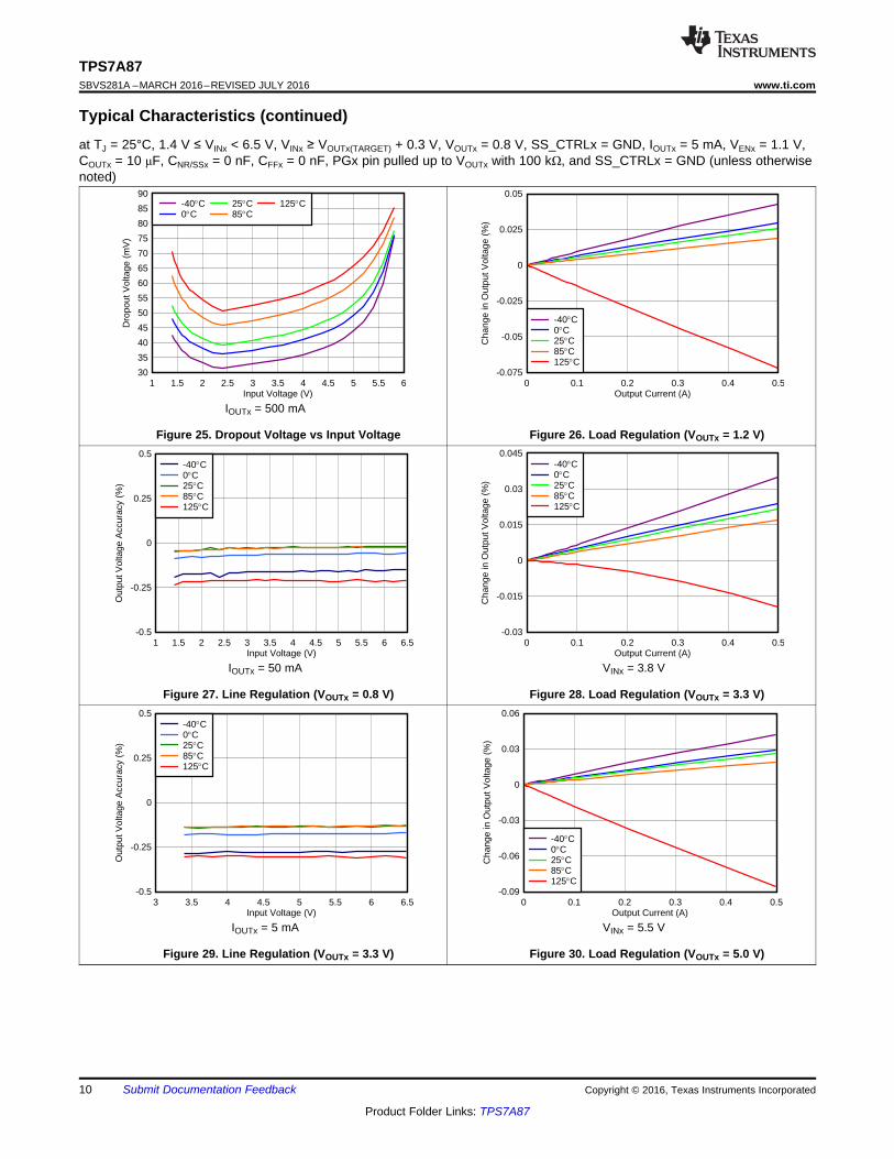
6.6 Typical Characteristicsat TJ = 25°C, 1.4 V ≤ VINx < 6.5 V, VINx ≥ VOUTx(TARGET) + 0.3 V, VOUTx = 0.8 V, SS_CTRLx = GND, IOUTx = 5 mA, VENx = 1.1 V,COUTx = 10 μF, CNR/SSx = 0 nF, CFFx = 0 nF, PGx pin pulled up to VOUTx with 100 kΩ, and SS_CTRLx = GND (unless otherwisenoted)
IOUTx = 500 mA, VINx = 5.3 V
Figure 1. Power-Supply Rejection Ratio at VOUTx = 5.0 V
VOUTx = 5 V, VINx = 5.3 V, VENx = 1.7 V, IOUTx = 500 mA,COUTx = 10 µF, CFFx = 10 nF
Figure 2. Power-Supply Rejection Ratio vsFrequency and CNR/SSx
VOUTx = 1.2 V, IOUTx = 500 mA, COUTx = 10 µF,CNR/SSx = CFFx = 10 nF
Figure 3. Power-Supply Rejection Ratio vsFrequency and Input Voltage
VOUTx = 1.2 V, VINx = 1.4 V, VENx = 3.8 V, IOUTx = 500 mA,COUTx = 10 µF, CNR/SSx = CFFx = 10 nF
Figure 4. Power-Supply Rejection Ratio vsFrequency and Output Current
VOUTx = 5.0 V, VINx = 5.3 V, VENx = 1.7 V, IOUTx = 500 mA,COUTx = ceramic, CFFx = 10 nF
Figure 5. Power-Supply Rejection Ratio vsFrequency and Output Capacitance
VOUTx = 1.8 V, IOUTx = 100 mA, COUTx = 10 µF,CNR/SSx = CFFx = 10 nF
Figure 6. Channel-to-Channel Output Voltage Isolation vsFrequency

Frequency (Hz)
Noi
se (P
V/
Hz)
1E+1 1E+2 1E+3 1E+4 1E+5 1E+6 1E+70.001
0.01
0.1
1
10CFFx = 0 PFCFFx = 0.01 PFCFFx = 0.1 PF
Frequency (Hz)
Noi
se (P
V/
Hz)
1E+1 1E+2 1E+3 1E+4 1E+5 1E+6 1E+70.001
0.01
0.1
1
10VINx = 1.5 VVINx = 1.8 VVINx = 2.5 VVINx = 3.3 V
Frequency (Hz)
Noi
se (P
V/
Hz)
1E+1 1E+2 1E+3 1E+4 1E+5 1E+6 1E+70.001
0.01
0.1
1
10VOUTx = 0.8 V, 3.94 PVRMSVOUTx = 1.2 V, 4.31 PVRMSVOUTx = 1.8 V, 5.1 PVRMSVOUTx = 2.5 V, 6.03 PVRMSVOUTx = 3.3 V, 7.43 PVRMSVOUTx = 5.0 V, 10.3 PVRMS
Frequency (Hz)
Noi
se (P
V/
Hz)
1E+1 1E+2 1E+3 1E+4 1E+5 1E+6 1E+70.001
0.01
0.1
1
10CNR/SSx = None, 11.43 PVRMSCNR/SSx = 0.01 PF, 4.94 PVRMSCNR/SSx = 0.1 PF, 4.24 PVRMSCNR/SSx = 1.0 PF, 4.22 PVRMS
Output Voltage (V)
Out
put V
otla
ge N
oise
(P
VR
MS)
0.8 1.6 2.4 3.2 4 4.8 5.64
6
8
10
12
14CFFx = 10 nF, CNR/SSx = 10 nFCFFx = 100 nF, CNR/SSx = 1 PF
Frequency
Out
put V
olta
ge N
oise
(P
V/
Hz)
0.00050.0010.002
0.0050.010.02
0.050.10.2
0.512
51020
50
10 100 1k 10k 100k 1M 10M
Nominal Noise FigureCNR/SSx = 1 PF, CFFx = 100 nFCNR/SSx = 1 PF, CFFx = 100 nF, SS_CTRLx = GNDCNR/SSx = 10 nF, CFFx = 10 nF, COUTx = 22 PF||1 mF
7
TPS7A87www.ti.com SBVS281A –MARCH 2016–REVISED JULY 2016
Product Folder Links: TPS7A87
Submit Documentation FeedbackCopyright © 2016, Texas Instruments Incorporated
Typical Characteristics (continued)at TJ = 25°C, 1.4 V ≤ VINx < 6.5 V, VINx ≥ VOUTx(TARGET) + 0.3 V, VOUTx = 0.8 V, SS_CTRLx = GND, IOUTx = 5 mA, VENx = 1.1 V,COUTx = 10 μF, CNR/SSx = 0 nF, CFFx = 0 nF, PGx pin pulled up to VOUTx with 100 kΩ, and SS_CTRLx = GND (unless otherwisenoted)
IOUTx = 500 mA
Figure 7. Output Noise vs Output Voltage
IOUTx = 500 mA
Figure 8. Output Noise at VOUTx = 5 V
VINx = VOUTx + 1.0 V, IOUTx = 500 mA, VRMS BW = 10 Hz to 100kHz, COUTx = 10 µF, CNR/SSx = CFFx = 10 nF
Figure 9. Noise vs Frequency and Output Voltage
VINx = 1.7 V, VOUTx = 1.2 V, IOUTx = 500 mA, VRMS BW = 10 Hz to100 kHz, COUTx = 10 µF, CFFx = 10 nF
Figure 10. Noise vs Frequency and CNR/SSx
VINx = 3.8 V, VOUTx = 3.3 V, IOUTx = 500 mA, VRMS BW = 10 Hz to100 kHz, COUTx = 10 µF, CNR/SSx = 10 nF
Figure 11. Noise vs Frequency and CFFx
VOUTx = 1.2 V, IOUTx = 500 mA, COUTx = 10 µF, CNR/SSx = 10 nF
Figure 12. Noise vs Frequency and VINx

VPGx
1 V/div
Time (200 Ps/div)
VINx
2 V/div
VOUTx
20 mV/div
Time (Ps)
AC
-Cou
pled
Out
put V
otla
ge (
mV
)
0 200 400 600 800 1000-50
-25
0
25
50IOUTx = 1 mA to 500 mAIOUTx = 10 mA to 500 mAIOUTx = 50 mA to 500 mAIOUTx = 100 mA to 500 mA
Feed-Forward Capacitor [CFFx] (PF)
RM
S O
utpu
t Noi
se (P
VR
MS)
1E-6 1E-5 0.0001 0.001 0.01 0.10
2
4
6
8
10
12
Time (Ps)
AC
-Cou
pled
Out
put V
olta
ge (
mV
)
Out
put C
urre
nt (
A)
0 200 400 600 800 1000-50 0
-25 0.5
0 1
25 1.5
50 2VOUTx = 5.0 VVOUTx = 3.3 V
VOUTx = 1.2 VVOUTx = 0.9 V
IOUTx
Frequency (Hz)
Noi
se (P
V/
Hz)
1E+1 1E+2 1E+3 1E+4 1E+5 1E+6 1E+70.001
0.01
0.1
1
10COUTx = 10 PF, 4.94 PVRMSCOUTx = 22 PF, 5.05 PVRMSCOUTx = 100 PF, 5.66 PVRMS
Noise Reduction Capacitor [CNR/SSx] (PF)
RM
S O
utpu
t Noi
se (P
VR
MS)
1E-6 1E-5 0.0001 0.001 0.01 0.1 1 100
2
4
6
8
10
12
8
TPS7A87SBVS281A –MARCH 2016–REVISED JULY 2016 www.ti.com
Product Folder Links: TPS7A87
Submit Documentation Feedback Copyright © 2016, Texas Instruments Incorporated
Typical Characteristics (continued)at TJ = 25°C, 1.4 V ≤ VINx < 6.5 V, VINx ≥ VOUTx(TARGET) + 0.3 V, VOUTx = 0.8 V, SS_CTRLx = GND, IOUTx = 5 mA, VENx = 1.1 V,COUTx = 10 μF, CNR/SSx = 0 nF, CFFx = 0 nF, PGx pin pulled up to VOUTx with 100 kΩ, and SS_CTRLx = GND (unless otherwisenoted)
VOUTx = 1.8 V, IOUTx = 500 mA, VRMS BW = 10 Hz to 100 kHz,CFFx = 0.01 µF
Figure 13. Noise vs Frequency and COUTx
VOUTx = 1.8 V, IOUTx = 500 mA, CFFx = 0.01 µF,BW = 10 Hz to 100 kHz
Figure 14. RMS Output Noise vs CNR/SSx
VOUTx = 1.8 V, IOUTx = 500 mA, CNR/SSx = 1 µF,BW = 10 Hz to 100 kHz
Figure 15. RMS Output Noise vs CFFx
VINx = VOUTx + 0.3 V, IOUTx = 10 mA to 500 mA, COUTx = 10 µF,CFFx = CNR/SSx = 10 nF
Figure 16. Load Transient Response vs VOUTx
VINx = 5.3 V, COUTx = 10 µF, CFFx = CNR/SSx = 10 nF
Figure 17. Load Transient Response vs DC Load
VINx = 1.4 V to 6.5 V to 1.4 V at 2 V/µs, VOUTx = 0.8 V,IOUTx = 500 mA, CNR/SSx = CFFx = 10 nF
Figure 18. Line Transient

Output Current (A)
Dro
pout
Vol
tage
(m
V)
0 0.1 0.2 0.3 0.4 0.50
20
40
60
80VINx = 1.4 VVINx = 1.8 VVINx = 3.6 V
VINx = 4.8 VVINx = 5.6 VVINx = 5.8 V
VPG1
200 mV/div
Time (2 ms/div)
VOUT1
200 mV/div
VEN1
1 V/div
VPG1
200 mV/div
Time (500Ps/div)
VOUT1
200 mV/div
VEN1
1 V/div
VPG1
200 mV/div
Time (50Ps/div)
VOUT1
200 mV/div
VEN1
1 V/div
Time (50 Ps/div)
VPGx
200mV/div
VOUTx
200 mV/div
VENx
1 V/div
Output Voltage (V)
Out
put C
urre
nt (
A)
0 0.5 1 1.5 2 2.5 3 3.50.9
0.95
1
1.05
1.1
1.15
1.2
1.25
-40qC 0qC 25qC 85qC 125qC
9
TPS7A87www.ti.com SBVS281A –MARCH 2016–REVISED JULY 2016
Product Folder Links: TPS7A87
Submit Documentation FeedbackCopyright © 2016, Texas Instruments Incorporated
Typical Characteristics (continued)at TJ = 25°C, 1.4 V ≤ VINx < 6.5 V, VINx ≥ VOUTx(TARGET) + 0.3 V, VOUTx = 0.8 V, SS_CTRLx = GND, IOUTx = 5 mA, VENx = 1.1 V,COUTx = 10 μF, CNR/SSx = 0 nF, CFFx = 0 nF, PGx pin pulled up to VOUTx with 100 kΩ, and SS_CTRLx = GND (unless otherwisenoted)
VINx = 3.4 V, VOUTx = 3.3 V, 125°C curve truncated because ofdevice entering thermal shutdown
Figure 19. Current Limit Foldback
VINx = 1.4 V
Figure 20. Start-Up (SS_CTRLx = GND, CNR/SSx = 0 nF)
VINx = 1.4 V
Figure 21. Start-Up (SS_CTRLx = GND, CNR/SSx = 10 nF)
VINx = 1.4 V
Figure 22. Start-Up (SS_CTRLx = VINx, CNR/SSx = 10 nF)
VINx = 1.4 V
Figure 23. Start-Up (SS_CTRLx = VINx, CNR/SSx = 1 µF)Figure 24. Dropout Voltage vs Output Current
Input Voltage (V)
Out
put V
olta
ge A
ccur
acy
(%)
3 3.5 4 4.5 5 5.5 6 6.5-0.5
-0.25
0
0.25
0.5-40qC0qC25qC85qC125qC
Output Current (A)
Cha
nge
in O
utpu
t Vol
tage
(%
)
0 0.1 0.2 0.3 0.4 0.5-0.09
-0.06
-0.03
0
0.03
0.06
-40qC0qC25qC85qC125qC
Input Voltage (V)
Out
put V
olta
ge A
ccur
acy
(%)
1 1.5 2 2.5 3 3.5 4 4.5 5 5.5 6 6.5-0.5
-0.25
0
0.25
0.5-40qC0qC25qC85qC125qC
Output Current (A)
Cha
nge
in O
utpu
t Vol
tage
(%
)
0 0.1 0.2 0.3 0.4 0.5-0.03
-0.015
0
0.015
0.03
0.045-40qC0qC25qC85qC125qC
Input Voltage (V)
Dro
pout
Vol
tage
(m
V)
1 1.5 2 2.5 3 3.5 4 4.5 5 5.5 630
35
40
45
50
55
60
65
70
75
80
85
90-40qC0qC
25qC85qC
125qC
Output Current (A)
Cha
nge
in O
utpu
t Vol
tage
(%
)
0 0.1 0.2 0.3 0.4 0.5-0.075
-0.05
-0.025
0
0.025
0.05
-40qC0qC25qC85qC125qC
10
TPS7A87SBVS281A –MARCH 2016–REVISED JULY 2016 www.ti.com
Product Folder Links: TPS7A87
Submit Documentation Feedback Copyright © 2016, Texas Instruments Incorporated
Typical Characteristics (continued)at TJ = 25°C, 1.4 V ≤ VINx < 6.5 V, VINx ≥ VOUTx(TARGET) + 0.3 V, VOUTx = 0.8 V, SS_CTRLx = GND, IOUTx = 5 mA, VENx = 1.1 V,COUTx = 10 μF, CNR/SSx = 0 nF, CFFx = 0 nF, PGx pin pulled up to VOUTx with 100 kΩ, and SS_CTRLx = GND (unless otherwisenoted)
IOUTx = 500 mA
Figure 25. Dropout Voltage vs Input Voltage Figure 26. Load Regulation (VOUTx = 1.2 V)
IOUTx = 50 mA
Figure 27. Line Regulation (VOUTx = 0.8 V)
VINx = 3.8 V
Figure 28. Load Regulation (VOUTx = 3.3 V)
IOUTx = 5 mA
Figure 29. Line Regulation (VOUTx = 3.3 V)
VINx = 5.5 V
Figure 30. Load Regulation (VOUTx = 5.0 V)

Temperature (qC)
%V
OU
Tx(
TA
RG
ET
)
-40 0 40 80 120 16088.5
88.8
89.1
89.4
89.7
90
VINx = 1.4 V, Falling ThresholdVINx = 1.4 V, Rising ThresholdVINx = 6.5 V, Falling ThresholdVINx = 6.5 V, Rising Threshold
PG Current (mA)
PG
Vol
tage
(m
V)
0 0.5 1 1.5 2 2.5 30
100
200
300
400
500-40qC0qC25qC85qC125qC
Input Voltage (V)
GN
D C
urre
nt (
mA
)
0.5 1 1.5 2 2.5 3 3.5 4 4.5 5 5.5 6 6.53
3.5
4
4.5
5
D001
-40qC0qC25qC85qC125qC
PG Current (mA)
PG
Vol
tage
(m
V)
0 0.5 1 1.5 2 2.5 30
100
200
300
400
500-40qC0qC25qC85qC125qC
Input Voltage (V)
Shu
tdow
n C
urre
nt (P
A)
1 1.5 2 2.5 3 3.5 4 4.5 5 5.5 6 6.50
1
2
3
4
5
D001
-40qC0qC25qC85qC125qC
Output Current (A)
Gro
und
Pin
Cur
rent
(m
A)
0 0.05 0.1 0.15 0.2 0.25 0.3 0.35 0.4 0.45 0.51.5
1.551.6
1.651.7
1.751.8
1.851.9
1.952
2.052.1
2.152.2
-40qC 0qC 25qC 85qC 125qC
11
TPS7A87www.ti.com SBVS281A –MARCH 2016–REVISED JULY 2016
Product Folder Links: TPS7A87
Submit Documentation FeedbackCopyright © 2016, Texas Instruments Incorporated
Typical Characteristics (continued)at TJ = 25°C, 1.4 V ≤ VINx < 6.5 V, VINx ≥ VOUTx(TARGET) + 0.3 V, VOUTx = 0.8 V, SS_CTRLx = GND, IOUTx = 5 mA, VENx = 1.1 V,COUTx = 10 μF, CNR/SSx = 0 nF, CFFx = 0 nF, PGx pin pulled up to VOUTx with 100 kΩ, and SS_CTRLx = GND (unless otherwisenoted)
Both channels
Figure 31. Shutdown Current vs Input Voltage
VINx = 1.4 V, both channels enabled
Figure 32. Ground Current vs Output Current
Both channels enabled
Figure 33. Ground Current vs Input Voltage Figure 34. PGx Low Level vs PGx Current (VINx = 1.4 V)
Figure 35. PGx Low Level vs PGx Current (VINx = 6.5 V) Figure 36. PGx Threshold vs Temperature

Temperature (qC)
Ena
ble
Thr
esho
ld (
V)
-40 0 40 80 120 1600.5
0.6
0.7
0.8
0.9
1VINx = 1.4 V, Falling ThresholdVINx = 1.4 V, Rising ThresholdVINx = 6.5 V, Falling ThresholdVINx = 6.5 V, Rising Threshold
Temperature (qC)
Inpu
t Vol
tage
(V
)
-40 -25 -10 5 20 35 50 65 80 95 110 1250.9
0.95
1
1.05
1.1
1.15
1.2
1.25
1.3
1.35
1.4Rising ThresholdFalling Threshold
Temperature (qC)
Cur
rent
(P
A)
-40 -25 -10 5 20 35 50 65 80 95 110 1250
0.005
0.01
0.015
0.02
0.025
0.03
Temperature (qC)
I NR
/SS
x
-40 0 40 80 120 1601
2
3
57
10
20
30
5070
100
200
VNx = 1.4 V, SS_CTRLx = GNDVNx = 1.4 V, SS_CTRLx = VINxVNx = 6.5 V, SS_CTRLx = GNDVNx = 6.5 V, SS_CTRLx = VINx
12
TPS7A87SBVS281A –MARCH 2016–REVISED JULY 2016 www.ti.com
Product Folder Links: TPS7A87
Submit Documentation Feedback Copyright © 2016, Texas Instruments Incorporated
Typical Characteristics (continued)at TJ = 25°C, 1.4 V ≤ VINx < 6.5 V, VINx ≥ VOUTx(TARGET) + 0.3 V, VOUTx = 0.8 V, SS_CTRLx = GND, IOUTx = 5 mA, VENx = 1.1 V,COUTx = 10 μF, CNR/SSx = 0 nF, CFFx = 0 nF, PGx pin pulled up to VOUTx with 100 kΩ, and SS_CTRLx = GND (unless otherwisenoted)
VINx = VPGx = 6.5 V
Figure 37. PGx Leakage Current vs Temperature Figure 38. Soft-Start Current vs Temperature(SS_CTRLx = GND)
Figure 39. Enable Threshold vs Temperature Figure 40. Input UVLOx Threshold vs Temperature

+
±
Charge Pump
Current Limit
0.8-V VREF
Thermal Shutdown
Error Amp
UVLO InternalEnableControl
SoftstartControl
OUT1
FB1
PG1
EN1
NR/SS1
SS_CTRL1
IN1
INR/SSx
GND
Active Discharge
+
±
0.89 x VREF
+
±
Charge Pump
Current Limit
0.8-V VREF
Thermal Shutdown
Error Amp
UVLO InternalEnableControl
SoftstartControl
OUT2
FB2
PG2
EN2
NR/SS2
SS_CTRL2
IN2
INR/SSx
Active Discharge
+
±
0.89 x VREF
13
TPS7A87www.ti.com SBVS281A –MARCH 2016–REVISED JULY 2016
Product Folder Links: TPS7A87
Submit Documentation FeedbackCopyright © 2016, Texas Instruments Incorporated
7 Detailed Description
7.1 OverviewThe TPS7A87 is a monolithic, dual-channel, low-dropout (LDO) regulator, and each channel is low-noise, high-PSRR, and capable of sourcing a 500-mA load with only 100 mV of maximum dropout. These features make thedevice a robust solution to solve many challenging problems in generating a clean, accurate power supply.
The various features for each of the TPS7A87 fully independent LDOs simplify using the device in a variety ofapplications. As detailed in the Functional Block Diagram section, these features are organized into threecategories, as shown in Table 1.
Table 1. FeaturesVOLTAGE REGULATION SYSTEM START-UP INTERNAL PROTECTION
High accuracy Programmable soft-start Foldback current limitLow-noise, high-PSRR output Sequencing controls
Thermal shutdownFast transient response Power-good output
7.2 Functional Block Diagram

+ ±
VINx To Load
VREF
GND
R1
R2
14
TPS7A87SBVS281A –MARCH 2016–REVISED JULY 2016 www.ti.com
Product Folder Links: TPS7A87
Submit Documentation Feedback Copyright © 2016, Texas Instruments Incorporated
7.3 Feature Description
7.3.1 Voltage Regulation Features
7.3.1.1 DC RegulationAn LDO functions as a class-B amplifier in which the input signal is the internal reference voltage (VREF), asshown in Figure 41. VREF is designed to have a very low-bandwidth at the input to the error amplifier through theuse of a low-pass filter (VNR/SSx).
As such, the reference can be considered as a pure dc input signal. The low output impedance of an LDO comesfrom the combination of the output capacitor and pass element. The pass element also presents a high inputimpedance to the source voltage when operating as a current source. A positive LDO can only source currentbecause of the class-B architecture.
This device achieves a maximum of 1% output voltage accuracy primarily because of the high-precision band-gap voltage (VBG) that creates VREF. The low dropout voltage (VDO) reduces the thermal power dissipationrequired by the device to regulate the output voltage at a given current level, thereby improving systemefficiency. Combined, these features help make this device a good approximation of an ideal voltage source.
This device replaces two stand-alone power-supplies, and also provides load-to-load isolation. The LDOs canalso be put in series (cascaded) to achieve even higher PSRR by connecting the output of one channel to theinput of the other channel.
NOTE: VOUTx = VREF × (1 + R1x / R2x).
Figure 41. Simplified Regulation Circuit
7.3.1.2 AC and Transient ResponseEach LDO responds quickly to a transient (large-signal response) on the input supply (line transient) or theoutput current (load transient) resulting from the LDO high-input impedance and low output-impedance acrossfrequency. This same capability also means that each LDO has a high power-supply rejection-ratio (PSRR) and,when coupled with a low internal noise-floor (Vn), the LDO approximates an ideal power supply in ac (small-signal) and large-signal conditions.
The performance and internal layout of the device minimizes the coupling of noise from one channel to the otherchannel (crosstalk). Good printed circuit board (PCB) layout minimizes the crosstalk.
The choice of external component values optimizes the small- and large-signal response. The NR/SSx capacitor(CNR/SSx) and feed-forward capacitor (CFFx) easily reduce the device noise floor and improve PSRR; see theOptimizing Noise and PSRR section for more information on optimizing the noise and PSRR performance.
7.3.2 System Start-Up FeaturesIn many different applications, the power-supply output must turn-on within a specific window of time to eitherensure proper operation of the load or to minimize the loading on the input supply or other sequencingrequirements. Each LDO start-up is well-controlled and user-adjustable, solving the demanding requirementsfaced by many power-supply design engineers in a simple fashion.

ENx
UVLOxInternal Enable Control
VREF
INR/SSx
RNRx
CNR/SSx
GND
+
±
SW
VFBx
NR/SSx Control
15
TPS7A87www.ti.com SBVS281A –MARCH 2016–REVISED JULY 2016
Product Folder Links: TPS7A87
Submit Documentation FeedbackCopyright © 2016, Texas Instruments Incorporated
Feature Description (continued)
(1) The active discharge remains on as long as VINx provides enough headroom for the discharge circuit to function.
7.3.2.1 Programmable Soft-Start (NR/SSx)Soft-start directly controls the output start-up time and indirectly controls the output current during start-up (in-rush current).
The external capacitor at the NR/SSx pin (CNR/SSx) sets the output start-up time by setting the rise time of theinternal reference (VNR/SSx), as shown in Figure 42. SS_CTRLx provides additional control over the rise time ofthe internal reference by enabling control over the charging current (INR/SSx) for CNR/SSx. The voltage at theSS_CTRLx pin (VSS_CTRLx) must be connected to ground (GND) or VINx.
Note that if CNR/SSx = 0 nF and the SS_CTRLx pin is connected to VINx, then the output voltage overshoots duringstart-up.
Figure 42. Simplified Soft-Start Circuit
7.3.2.2 SequencingControlling when a single power supply turns on can be difficult in a power distribution network (PDN) because ofthe high power levels inherent in a PDN, and the variations between all of the supplies. Control of each channelturn-on and turn-off time is set by the specific channel enable circuit (ENx) and undervoltage lockout circuit(UVLOx), as shown in Figure 43 and Table 2.
Figure 43. Simplified Turn-On Control
Table 2. Sequencing Functionality Table
INPUT VOLTAGE ENABLE STATUS LDOSTATUS
ACTIVEDISCHARGE POWER-GOOD
VINx ≥ VUVLOxENx = 1 On Off PGx = 1 when VOUTx ≥ VIT(PGx)
ENx = 0 Off On PGx = 0VINx < VUVLOx – VHYS ENx = don't care Off On (1) PGx = 0
7.3.2.2.1 Enable (ENx)
The enable signal (VENx) is an active-high digital control that enables the LDO when the enable voltage is pastthe rising threshold (VENx ≥ VIH(ENx)) and disables the LDO when the enable voltage is below the falling threshold(VENx ≤ VIL(ENx)). The exact enable threshold is between VIH(ENx) and VIL(ENx) because ENx is a digital control. Inapplications that do not use the enable control, connect ENx to VINx.

GND
VBG
+
±
VINx
VFBx
GND
VPGx
ENxGNDUVLOx
16
TPS7A87SBVS281A –MARCH 2016–REVISED JULY 2016 www.ti.com
Product Folder Links: TPS7A87
Submit Documentation Feedback Copyright © 2016, Texas Instruments Incorporated
7.3.2.2.2 Undervoltage Lockout (UVLOx) Control
The UVLOx circuit responds quickly to glitches on VINx and attempts to disable the output of the device if eitherof these rails collapse.
As a result of the fast response time of the input supply UVLOx circuit, fast and short line transients well belowthe input supply UVLOx falling threshold (brownouts) can cause momentary glitches during the edges of thetransient. These glitches are typical in most LDOs and, in most applications, the brownouts required for theseglitches do not result from the local input capacitance; see the Undervoltage Lockout (UVLOx) Control section formore details.
7.3.2.2.3 Active Discharge
When either ENx or UVLOx is low, the device connects a resistor of several hundred ohms from VOUTx to GND,discharging the output capacitance.
Do not rely on the active discharge circuit for discharging large output capacitors when the input voltage dropsbelow the targeted output voltage. Current flows from the output to the input (reverse current) when VOUTx > VINx,which can cause damage to the device (when VOUTx > VINx + 0.3 V); see the Reverse Current Protection sectionfor more details.
7.3.2.3 Power-Good Output (PGx)The PGx signal provides an easy solution to meet demanding sequencing requirements because PGx signalswhen the output nears its nominal value. PGx can be used to signal other devices in a system when the outputvoltage is near, at, or above the set output voltage (VOUTx(Target)). A simplified schematic is shown in Figure 44.
The PGx signal is an open-drain digital output that requires a pullup resistor to a voltage source and is activehigh. The power-good circuit sets the PGx pin into a high-impedance state to indicate that the power is good.
Using a large feed-forward capacitor (CFFx) delays the output voltage and, because the power-good circuitmonitors the FBx pin, the PGx signal can indicate a false positive. A simple solution to this scenario is to use anexternal voltage detector device, such as the TPS3780; see the Feed-Forward Capacitor (CFFx) section for moreinformation.
Figure 44. Simplified PGx Circuit

17
TPS7A87www.ti.com SBVS281A –MARCH 2016–REVISED JULY 2016
Product Folder Links: TPS7A87
Submit Documentation FeedbackCopyright © 2016, Texas Instruments Incorporated
(1) All table conditions must be met.(2) The device is disabled when any condition is met.
7.3.3 Internal Protection FeaturesIn many applications, fault events can occur that damage devices in the system. Short-circuits and excessiveheat are the most common fault events for power supplies. The TPS7A87 implements circuitry for each LDO toprotect the device and its load during these events. Continuously operating in these fault conditions or above ajunction temperature of 125°C is not recommended because the long-term reliability of the device is reduced.
7.3.3.1 Foldback Current Limit (ICLx)The internal current limit circuit protects the LDO against short-circuit and excessive load current conditions. Theoutput current decreases (folds back) when the output voltage falls to better protect the device, as described inFigure 19. Each channel features its own independent current limit circuit.
7.3.3.2 Thermal Protection (Tsdx)The thermal shutdown circuit protects the LDO against excessive heat in the system, either resulting from currentlimit or high ambient temperature. Each channel features its own independent thermal shutdown circuit.
The output of the LDO turns off when the LDO temperature (junction temperature, TJ) exceeds the rising thermalshutdown temperature (Tsdx). The output turns on again after TJ decreases below the falling thermal shutdowntemperature (Tsdx).
A high power dissipation across the device, combined with a high ambient temperature (TA), can cause TJ to begreater than or equal to Tsdx, triggering the thermal shutdown and causing the output to fall to 0 V. The LDO cancycle on and off when thermal shutdown is reached under these conditions.
7.4 Device Functional ModesTable 3 provides a quick comparison between the regulation and disabled operation.
Table 3. Device Functional Modes Comparison
OPERATING MODEPARAMETER
VINx ENx IOUTx TJ
Regulation (1) VINx > VOUTx(nom) + VDO VENx > VIH(ENx) IOUTx < ICLx TJ < Tsd
Disabled (2) VINx < VUVLOx VENx < VIL(ENx) — TJ > Tsd
7.4.1 RegulationThe device regulates the output to the targeted output voltage when all the conditions in Table 3 are met.
7.4.2 DisabledWhen disabled, the pass device is turned off, the internal circuits are shutdown, and the output voltage is activelydischarged to ground by an internal resistor from the output to ground.

VOUT1VIN1 OUT1
PG1
IN1
EN1
TPS7A87
SS_CTRL1
NR/SS1
FB1CIN1 COUT1
CNR/SS1
R11
R21
OUT2
PG2
IN2
EN2
SS_CTRL2
NR/SS2
FB2
GND
VOUT2
COUT2R12
R22
VIN2
CIN2
CNR/SS2
Copyright © 2016, Texas Instruments Incorporated
18
TPS7A87SBVS281A –MARCH 2016–REVISED JULY 2016 www.ti.com
Product Folder Links: TPS7A87
Submit Documentation Feedback Copyright © 2016, Texas Instruments Incorporated
8 Application and Implementation
NOTEInformation in the following applications sections is not part of the TI componentspecification, and TI does not warrant its accuracy or completeness. TI’s customers areresponsible for determining suitability of components for their purposes. Customers shouldvalidate and test their design implementation to confirm system functionality.
8.1 Application InformationSuccessfully implementing an LDO in an application depends on the application requirements. This sectiondiscusses key device features and how to best implement them to achieve a reliable design.
8.1.1 External Component Selection
8.1.1.1 Setting the Output Voltage (Adjustable Operation)Each LDO resistor feedback network sets the output voltage, as shown in Figure 45, with an output voltagerange of 0.8 V to 5.2 V.
Figure 45. Adjustable Operation
Equation 1 relates the values R1x and R2x to VOUTx(Target) and VFBx. Equation 1 is a rearranged version ofEquation 2, simplifying the feedback resistor calculation. The current through the feedback network must beequal to or greater than 5 μA for optimum noise performance and accuracy, as shown in Equation 3.
VOUTx = VFBx × (1 + R1x / R2x) (1)R1x = (VOUTx / VFBx – 1) × R2x (2)R2x < VREF / 5 µA (3)
The input bias current into the error amplifier (feedback pin current, IFBx) and tighter tolerance resistors must betaken into account for optimizing the output voltage accuracy.

19
TPS7A87www.ti.com SBVS281A –MARCH 2016–REVISED JULY 2016
Product Folder Links: TPS7A87
Submit Documentation FeedbackCopyright © 2016, Texas Instruments Incorporated
Application Information (continued)
(1) R1x is connected from OUTx to FBx; R2x is connected from FBx to GND; see Figure 45.
Table 4 shows the resistor combinations for several common output voltages using commercially-available, 1%tolerance resistors.
Table 4. Recommended Feedback-Resistor Values
TARGETED OUTPUTVOLTAGE (V)
FEEDBACK RESISTOR VALUES (1) CALCULATED OUTPUTVOLTAGE (V)R1x (kΩ) R2x (kΩ)
0.80 Short Open 0.8000.90 1.37 11.0 0.9000.95 1.91 10.2 0.9501.00 2.55 10.2 1.0001.05 3.32 10.7 1.0481.10 3.57 9.53 1.1001.15 4.64 10.7 1.1471.20 5.49 11.0 1.1991.35 6.98 10.2 1.3471.50 9.31 10.7 1.4961.80 13.70 11.0 1.7961.90 14.70 10.7 1.8992.50 22.60 10.7 2.4902.85 27.40 10.7 2.8493.00 29.40 10.7 2.9983.30 33.20 10.7 3.2823.60 35.70 10.2 3.6004.50 44.20 9.53 4.5105.00 56.20 10.7 5.0025.20 53.60 9.76 5.193
8.1.1.2 Capacitor RecommendationsThe device is designed to be stable using low equivalent series resistance (ESR) ceramic capacitors at the inputand output pins. Multilayer ceramic capacitors have become the industry standard for these types of applicationsand are recommended, but must be used with good judgment. Ceramic capacitors that employ X7R-, X5R-, andCOG-rated dielectric materials provide relatively good capacitive stability across temperature, whereas the use ofY5V-rated capacitors is discouraged because of large variations in capacitance.
Regardless of the ceramic capacitor type selected, ceramic capacitance varies with operating voltage andtemperature. As a rule of thumb, derate ceramic capacitors by at least 50%. The input and output capacitorsrecommended herein account for an effective capacitance derating of approximately 50%, but at higher VINx andVOUTx conditions (that is, VINx = 5.5 V to VOUTx = 5.0 V) the derating can be greater than 50% and must be takeninto consideration.
8.1.1.3 Input and Output Capacitor (CINx and COUTx)The device is designed and characterized for operation with ceramic capacitors of 10 µF or greater (5 µF orgreater of effective capacitance) at each input and output. Locate the input and output capacitors as near aspractical to the respective input and output pins to minimize the trace inductance from the capacitor to thedevice.

I =OUTx(t)
COUTx OUTx´ dV (t)
dt
VOUTx(t)
RLOAD
+
20
TPS7A87SBVS281A –MARCH 2016–REVISED JULY 2016 www.ti.com
Product Folder Links: TPS7A87
Submit Documentation Feedback Copyright © 2016, Texas Instruments Incorporated
8.1.1.4 Feed-Forward Capacitor (CFFx)Although a feed-forward capacitor (CFFx) from the FBx pin to the OUTx pin is not required to achieve stability, a10-nF external CFFx optimizes the transient, noise, and PSRR performance. A higher capacitance CFFx can beused; however, the start-up time is longer and the power-good signal can incorrectly indicate that the outputvoltage is settled. The maximum recommended value is 100 nF.
To ensure proper PGx functionality, the time constant defined by CNR/SSx must be greater than or equal to thetime constant from CFFx. For a detailed description, see the Pros and Cons of Using a Feed-Forward Capacitorwith a Low Dropout Regulator application report (SBVA042).
8.1.1.5 Noise-Reduction and Soft-Start Capacitor (CNR/SSx)Although a noise-reduction and soft-start capacitor (CNR/SSx) from the NR/SSx pin to GND is not required, CNR/SSxis highly recommended to control the start-up time and reduce the noise-floor of the device. The typical valueused is 10 nF, and the maximum recommended value is 10 µF.
8.1.2 Start-Up
8.1.2.1 Circuit Soft-Start Control (NR/SSx)Each output of the device features a user-adjustable, monotonic, voltage-controlled soft-start that is set with anexternal capacitor (CNR/SSx). This soft-start eliminates power-up initialization problems when powering field-programmable gate arrays (FPGAs), digital signal processors (DSPs), or other processors. The controlledvoltage ramp of the output also reduces peak inrush current during start-up, thus minimizing start-up transients tothe input power bus.
The output voltage (VOUTx) rises proportionally to VNR/SSx during start-up as the LDO regulates so that thefeedback voltage equals the NR/SSx voltage (VFBx = VNR/SSx). As such, the time required for VNR/SSx to reach itsnominal value determines the rise time of VOUTx (start-up time).
The soft-start ramp time depends on the soft-start charging current (INR/SSx), the soft-start capacitance (CNR/SSx),and the internal reference (VREF). The approximate soft-start ramp time (tSSx) can be calculated with Equation 4:
tSSx = (VREF × CNR/SSx) / INR/SSx (4)
The SS_CTRLx pin for each output sets the value of the internal current source, maintaining a fast start-up timeeven with a large CNR/SSx capacitor. When the SS_CTRLx pin is connected to GND, the typical value for theINR/SSx current is 6.2 µA. Connecting the SS_CTRLx pin to INx increases the typical soft-start charging current to100 µA. The larger charging current for INR/SSx is useful when smaller start-up ramp times are needed or whenusing larger noise-reduction capacitors.
Not using a noise-reduction capacitor on the NR/SSx pin and tying the SS_CTRLx pin to VINx results in outputvoltage overshoot of approximately 10%. Connecting the SS_CTRLx pin to GND or using a capacitor on theNR/SSx pin minimizes the overshoot.
Values for the soft-start charging currents are provided in the Electrical Characteristics table.
8.1.2.1.1 In-Rush Current
In-rush current is defined as the current into the LDO at the INx pin during start-up. In-rush current then consistsprimarily of the sum of load current and the current used to charge the output capacitor. This current is difficult tomeasure because the input capacitor must be removed, which is not recommended. However, this soft-startcurrent can be estimated by Equation 5:
where:• VOUTx(t) is the instantaneous output voltage of the turn-on ramp• dVOUTx(t) / dt is the slope of the VOUTx ramp• RLOAD is the resistive load impedance (5)
C
tAt
VINx
VOUTx
UVLOx Rising Threshold
UVLOx Hysteresis
tBt tDt tEt tFt tGt
21
TPS7A87www.ti.com SBVS281A –MARCH 2016–REVISED JULY 2016
Product Folder Links: TPS7A87
Submit Documentation FeedbackCopyright © 2016, Texas Instruments Incorporated
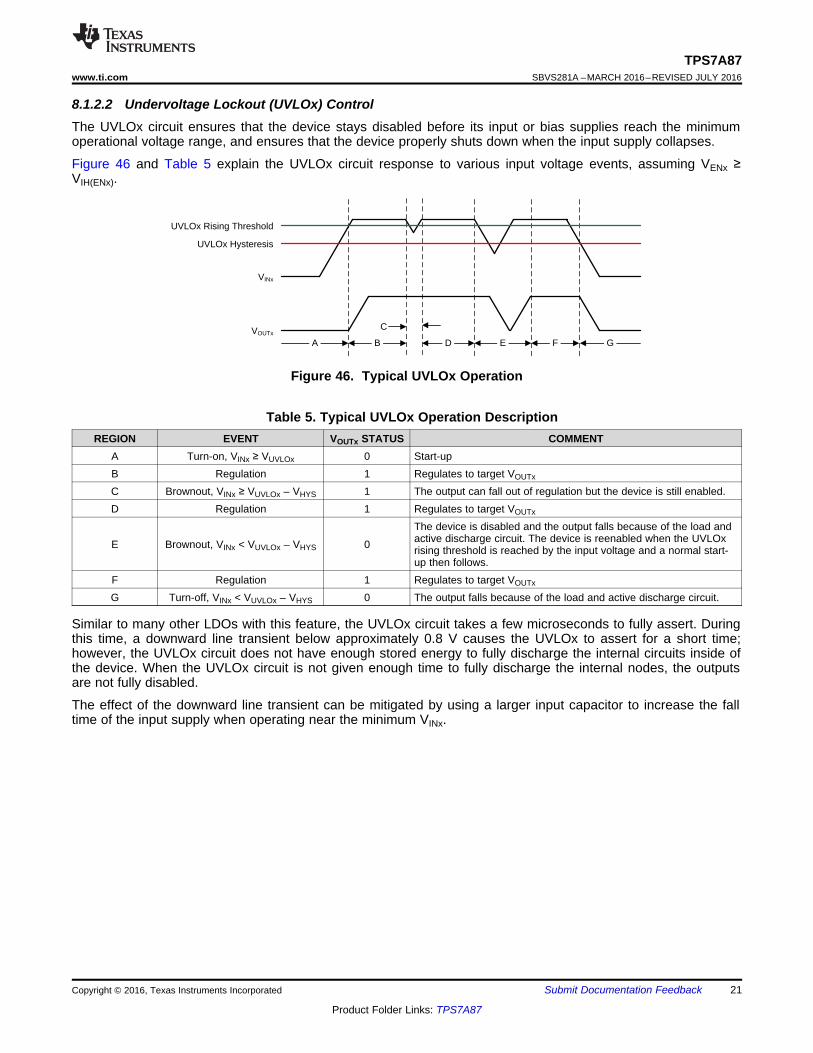
8.1.2.2 Undervoltage Lockout (UVLOx) ControlThe UVLOx circuit ensures that the device stays disabled before its input or bias supplies reach the minimumoperational voltage range, and ensures that the device properly shuts down when the input supply collapses.
Figure 46 and Table 5 explain the UVLOx circuit response to various input voltage events, assuming VENx ≥VIH(ENx).
Figure 46. Typical UVLOx Operation
Table 5. Typical UVLOx Operation DescriptionREGION EVENT VOUTx STATUS COMMENT
A Turn-on, VINx ≥ VUVLOx 0 Start-upB Regulation 1 Regulates to target VOUTx
C Brownout, VINx ≥ VUVLOx – VHYS 1 The output can fall out of regulation but the device is still enabled.D Regulation 1 Regulates to target VOUTx
E Brownout, VINx < VUVLOx – VHYS 0
The device is disabled and the output falls because of the load andactive discharge circuit. The device is reenabled when the UVLOxrising threshold is reached by the input voltage and a normal start-up then follows.
F Regulation 1 Regulates to target VOUTx
G Turn-off, VINx < VUVLOx – VHYS 0 The output falls because of the load and active discharge circuit.
Similar to many other LDOs with this feature, the UVLOx circuit takes a few microseconds to fully assert. Duringthis time, a downward line transient below approximately 0.8 V causes the UVLOx to assert for a short time;however, the UVLOx circuit does not have enough stored energy to fully discharge the internal circuits inside ofthe device. When the UVLOx circuit is not given enough time to fully discharge the internal nodes, the outputsare not fully disabled.
The effect of the downward line transient can be mitigated by using a larger input capacitor to increase the falltime of the input supply when operating near the minimum VINx.

C
tAt
VOUTx
PGx
PGx Rising Threshold
PGx Falling Threshold
tBt tDt tFt tGt
E
22
TPS7A87SBVS281A –MARCH 2016–REVISED JULY 2016 www.ti.com
Product Folder Links: TPS7A87
Submit Documentation Feedback Copyright © 2016, Texas Instruments Incorporated
8.1.2.3 Power-Good (PGx) FunctionThe power-good circuit monitors the voltage at the feedback pin to indicate the status of the output voltage. Thepower-good circuit asserts whenever FBx, VINx, or ENx are below their thresholds. The PGx operation versus theoutput voltage is shown in Figure 47, which is described by Table 6.
Figure 47. Typical PGx Operation
Table 6. Typical PGx Operation DescriptionREGION EVENT PGx STATUS FBx VOLTAGE
A Turn-on 0 VFBx < VIT(PGx) + VHYS(PGx)
B Regulation Hi-ZVFBx ≥ VIT(PGx)C Output voltage dip Hi-Z
D Regulation Hi-ZE Output voltage dip 0 VFBx < VIT(PGx)
F Regulation Hi-Z VFBx ≥ VIT(PGx)
G Turn-off 0 VFBx < VIT(PGx)
The PGx pin is open-drain and connecting a pullup resistor to an external supply enables others devices toreceive power-good as a logic signal that can be used for sequencing. Make sure that the external pullup supplyvoltage results in a valid logic signal for the receiving device or devices.
To ensure proper operation of the power-good circuit, the pullup resistor value must be between 10 kΩ and100 kΩ. The lower limit of 10 kΩ results from the maximum pulldown strength of the power-good transistor, andthe upper limit of 100 kΩ results from the maximum leakage current at the power-good node. If the pullup resistoris outside of this range, then the power-good signal may not read a valid digital logic level.
Using a large CFFx with a small CNR/SSx causes the power-good signal to incorrectly indicate that the outputvoltage has settled during turn-on. The CFFx time constant must be greater than the soft-start time constant toensure proper operation of the PGx during start-up. For a detailed description, see the Pros and Cons of Using aFeed-Forward Capacitor with a Low Dropout Regulator application report (SBVA042).
The state of PGx is only valid when the device operates above the minimum supply voltage. During shortbrownout events and at light loads, power-good does not assert because the output voltage (therefore VFBx) issustained by the output capacitance.
8.1.3 AC and Transient PerformanceLDO ac performance for a dual-channel device includes power-supply rejection ratio, channel-to-channel outputisolation, output current transient response, and output noise. These metrics are primarily a function of open-loopgain, bandwidth, and phase margin that control the closed-loop input and output impedance of the LDO. Theoutput noise is primarily a result of the reference and error amplifier noise.

Pow
er-S
uppl
y R
ejec
tion
Rat
io (
dB)
Frequency (Hz)
Band Gap Band-Gap RC Filter
Error Amplifier, Flat-Gain Region
Error Amplifier, Gain Roll-Off
Output Capacitor |ZCOUTx| Decreasing
Output Capacitor |ZCOUTx| Increasing
PSRR Boost Circuit Improves PSRR in This Region
Sub 10 Hz 10 Hz±1 MHz100 kHz +
INx10
OUTx
V (f)PSRR (dB) 20 Log
V (f )
§ · ¨ ¸
© ¹
23
TPS7A87www.ti.com SBVS281A –MARCH 2016–REVISED JULY 2016
Product Folder Links: TPS7A87
Submit Documentation FeedbackCopyright © 2016, Texas Instruments Incorporated
8.1.3.1 Power-Supply Rejection Ratio (PSRR)PSRR is a measure of how well the LDO control-loop rejects signals from VINx to VOUTx across the frequencyspectrum (usually 10 Hz to 10 MHz). Equation 6 gives the PSRR calculation as a function of frequency for theinput signal [VINx(f)] and output signal [VOUTx(f)].
(6)
Even though PSRR is a loss in signal amplitude, PSRR is shown as positive values in decibels (dB) forconvenience.
A simplified diagram of PSRR versus frequency is shown in Figure 48.
Figure 48. Power-Supply Rejection Ratio Diagram
An LDO is often employed not only as a dc-dc regulator, but also to provide exceptionally clean power-supplyvoltages that exhibit ultra-low noise and ripple to sensitive system components. This usage is especially true forthe TPS7A87.
The TPS7A87 features an innovative circuit to boost the PSRR between 200 kHz and 1 MHz; see Figure 4. Toachieve the maximum benefit of this PSRR boost circuit, using a capacitor with a minimum impedance in the100-kHz to 1-MHz band is recommended.
8.1.3.2 Channel-to-Channel Output Isolation and CrosstalkOutput isolation is a measure of how well the device prevents voltage disturbances on one output from affectingthe other output. This attenuation appears in load transient tests on the other output; however, to numericallyquantify the rejection, the output channel isolation is expressed in decibels (dB).
Output isolation performance is a strong function of the PCB layout. See the Layout section on how to bestoptimize the isolation performance.

Out
put V
olta
ge N
oise
Den
sity
(nV
/¥+])
Frequency (Hz)
Integrated NoiseFrom Band-Gap and Error Amplifier
Measurement Noise Floor
1/f Noise
Wide-Band Noise
Noise Gain Roll-Off
Charge Pump Spurs
24
TPS7A87SBVS281A –MARCH 2016–REVISED JULY 2016 www.ti.com
Product Folder Links: TPS7A87
Submit Documentation Feedback Copyright © 2016, Texas Instruments Incorporated
(1) The number of +'s indicates the improvement in noise or PSRR performance by increasing the parameter value.(2) Shaded cells indicate the easiest improvement to noise or PSRR performance.
8.1.3.3 Output Voltage NoiseThe TPS7A87 is designed for system applications where minimizing noise on the power-supply rail is critical tosystem performance. For example, the TPS7A87 can be used in a phase-locked loop (PLL)-based clockingcircuit can be used for minimum phase noise, or in test and measurement systems where even small power-supply noise fluctuations reduce system dynamic range.
LDO noise is defined as the internally-generated intrinsic noise created by the semiconductor circuits alone. Thisnoise is the sum of various types of noise (such as shot noise associated with current-through-pin junctions,thermal noise caused by thermal agitation of charge carriers, flicker noise, or 1/f noise and dominates at lowerfrequencies as a function of 1/f). Figure 49 shows a simplified output voltage noise density plot versus frequency.
Figure 49. Output Voltage Noise Diagram
For further details, see the How to Measure LDO Noise white paper (SLYY076).
8.1.3.4 Optimizing Noise and PSRRThe ultra-low noise floor and PSRR of the device can be improved in several ways, as described in Table 7.
Table 7. Effect of Various Parameters on AC Performance (1) (2)
PARAMETERNOISE PSRR
LOW-FREQUENCY
MID-FREQUENCY
HIGH-FREQUENCY
LOW-FREQUENCY
MID-FREQUENCY
HIGH-FREQUENCY
CNR/SSx +++ No effect No effect +++ + No effectCFFx ++ +++ + ++ +++ +
COUTx No effect + +++ No effect + +++VINx – VOUTx + + + +++ +++ ++PCB layout ++ ++ + + +++ +++
The noise-reduction capacitor, in conjunction with the noise-reduction resistor, forms a low-pass filter (LPF) thatfilters out the noise from the reference before being gained up with the error amplifier, thereby minimizing theoutput voltage noise floor. The LPF is a single-pole filter and the cutoff frequency can be calculated withEquation 7. The typical value of RNR is 250 kΩ. The effect of the CNR/SSx capacitor increases when VOUTx(Target)increases because the noise from the reference is gained up when the output voltage increases. For low-noiseapplications, a 10-nF to 10-µF CNR/SSx is recommended.
fcutoff = 1 / (2 × π × RNR × CNR/SSx) (7)
The feed-forward capacitor reduces output voltage noise by filtering out the mid-band frequency noise. The feed-forward capacitor can be optimized by placing a pole-zero pair near the edge of the loop bandwidth and pushingout the loop bandwidth, thus improving mid-band PSRR.

25
TPS7A87www.ti.com SBVS281A –MARCH 2016–REVISED JULY 2016
Product Folder Links: TPS7A87
Submit Documentation FeedbackCopyright © 2016, Texas Instruments Incorporated
A larger COUTx or multiple output capacitors reduces high-frequency output voltage noise and PSRR by reducingthe high-frequency output impedance of the power supply.
Additionally, a higher input voltage improves the noise and PSRR because greater headroom is provided for theinternal circuits. However, a high power dissipation across the die increases the output noise because of theincrease in junction temperature.
Good PCB layout improves the PSRR and noise performance by providing heatsinking at low frequencies andisolating VOUTx at high frequencies.
Table 8 lists the output voltage noise for the 10-Hz to 100-kHz band at a 5-V output for a variety of conditionswith an input voltage of 5.4 V, an R1x of 12.1 kΩ, and a load current of 0.5 A. The 5-V output is chosen becausethis output is the worst-case condition for output voltage noise.
Table 8. Output Noise Voltage at a 5-V Output with a 5.4-V Input
CNR/SSx (nF) CFFx (nF) COUTx (µF) SS_CTRLx OUTPUT VOLTAGENOISE (µVRMS)
10 10 22 VINx 10.81000 100 22 VINx 5.61000 100 22 GND 5.61000 100 22 || 1000 VINx 5.0
8.1.3.4.1 Charge Pump Noise
The device internal charge pump generates a minimal amount of noise.
The high-frequency components of the output voltage noise density curve are filtered out in most applications byusing 10-nF to 100-nF bypass capacitors close to the load. Using a ferrite bead between the LDO output and theload input capacitors forms a pi-filter, further reducing the high-frequency noise contribution.

FB
VOUTx
IOUTx
HGECA D
26
TPS7A87SBVS281A –MARCH 2016–REVISED JULY 2016 www.ti.com
Product Folder Links: TPS7A87
Submit Documentation Feedback Copyright © 2016, Texas Instruments Incorporated
8.1.3.5 Load Transient ResponseThe load-step transient response is the output voltage response by the LDO to a step in load current, wherebyoutput voltage regulation is maintained. There are two key transitions during a load transient response: thetransition from a light to a heavy load and the transition from a heavy to a light load. The regions shown inFigure 50 are broken down in this section and are described in Table 9. Regions A, E, and H are where theoutput voltage is in steady-state.
Figure 50. Load Transient Waveform
Table 9. Load Transient Waveform DescriptionREGION DESCRIPTION COMMENT
A Regulation RegulationB Output current ramping Initial voltage dip is a result of the depletion of the output capacitor charge.
C LDO responding to transient Recovery from the dip results from the LDO increasing its sourcing current, and leadsto output voltage regulation.
D Reaching thermal equilibrium At high load currents the LDO takes some time to heat up. During this time the outputvoltage changes slightly.
E Regulation Regulation
F Output current ramping Initial voltage rise results from the LDO sourcing a large current, and leads to theoutput capacitor charge to increase.
G LDO responding to transient Recovery from the rise results from the LDO decreasing its sourcing current incombination with the load discharging the output capacitor.
H Regulation Regulation

VDO
IOUTx
Slope
= ~R
DS(ON)
VOUTx
IOUTx
Wrise
Wfall
VOUTx(max)
VOUTx(min)
IOUTx(HI)
IOUTx(LO)IOUTx(LO)
trise
PW
tfall
27
TPS7A87www.ti.com SBVS281A –MARCH 2016–REVISED JULY 2016
Product Folder Links: TPS7A87
Submit Documentation FeedbackCopyright © 2016, Texas Instruments Incorporated
The transient response peaks (VOUTx(max) and VOUTx(min)) are improved by using more output capacitance;however, doing so slows down the recovery time (Wrise and Wfall). Figure 51 shows these parameters during aload transient, with a given pulse duration (PW) and current levels (IOUTx(LO) and IOUTx(HI)).
Figure 51. Simplified Load Transient Waveform
8.1.4 DC Performance
8.1.4.1 Output Voltage Accuracy (VOUTx)The device features an output voltage accuracy of 1% maximum that includes the errors introduced by theinternal reference, load regulation, line regulation, and operating temperature as specified by the ElectricalCharacteristics table. Output voltage accuracy specifies minimum and maximum output voltage error, relative tothe expected nominal output voltage stated as a percent.
8.1.4.2 Dropout Voltage (VDO)Generally speaking, the dropout voltage often refers to the minimum voltage difference between the input andoutput voltage (VDO = VINx – VOUTx) that is required for regulation. When VINx drops below the required VDO forthe given load current, the device functions as a resistive switch and does not regulate output voltage. Dropoutvoltage is proportional to the output current because the device is operating as a resistive switch, as shown inFigure 52.
Figure 52. Dropout Voltage versus Output Current
Dropout voltage is affected by the drive strength for the gate of the pass element, which is nonlinear with respectto VINx on this device because of the internal charge pump. Dropout voltage increases exponentially when theinput voltage nears its maximum operating voltage because the charge pump multiplies the input voltage by afactor of 4 and then is internally clamped to 8.0 V.
8.1.4.2.1 Behavior when Transitioning from Dropout into Regulation
Some applications can have transients that place the LDO into dropout, such as slower ramps on VINX for start-up or load transients. As with many other LDOs, the output can overshoot on recovery from these conditions.

TI Device
INx OUTx
GND
COUTx
CINx
Schottky Diode
Internal Body Diode
Copyright © 2016, Texas Instruments Incorporated
Input Voltage
Output Voltage
Output Voltage in normal regulation.
Dropout VOUTx = VINx - VDO
VINx = VOUTx(nom) + VDO
Response time for LDO to get back into
regulation. Load current discharges output voltage.
Vol
tage
Time
28
TPS7A87SBVS281A –MARCH 2016–REVISED JULY 2016 www.ti.com
Product Folder Links: TPS7A87
Submit Documentation Feedback Copyright © 2016, Texas Instruments Incorporated
A ramping input supply can cause an LDO to overshoot on start-up when the slew rate and voltage levels are inthe right range, as shown in Figure 53. This condition is easily avoided through either the use of an enablesignal, or by increasing the soft-start time with CSS/NRx.
Figure 53. Start-Up Into Dropout
8.1.5 Reverse Current ProtectionAs with most LDOs, this device can be damaged by excessive reverse current.
Reverse current is current that flows through the body diode on the pass element instead of the normalconducting channel. This current flow, at high enough magnitudes, degrades long-term reliability of the deviceresulting from risks of electromigration and excess heat being dissipated across the device. If the current flowgets high enough, a latch-up condition can be entered.
Conditions where excessive reverse current can occur are outlined in this section, all of which can exceed theabsolute maximum rating of VOUTx > VINx + 0.3 V:• If the device has a large COUTx and the input supply collapses quickly with little or no load current• The output is biased when the input supply is not established• The output is biased above the input supplyIf excessive reverse current flow is expected in the application, then external protection must be used to protectthe device. Figure 54 shows one approach of protecting the device.
Figure 54. Example Circuit for Reverse Current Protection Using a Schottky Diode

Y
Y Y ´
JT J T JT D: T = T + PY ´
JB J B JB D: T = T + P
29
TPS7A87www.ti.com SBVS281A –MARCH 2016–REVISED JULY 2016
Product Folder Links: TPS7A87
Submit Documentation FeedbackCopyright © 2016, Texas Instruments Incorporated
8.1.6 Power Dissipation (PD)Circuit reliability demands that proper consideration is given to device power dissipation, location of the circuit onthe printed circuit board (PCB), and correct sizing of the thermal plane. The PCB area around the regulator mustbe as free as possible of other heat-generating devices that cause added thermal stresses.
As a first-order approximation, power dissipation in the regulator depends on the input-to-output voltagedifference and load conditions. PD can be approximated using Equation 8:
PD = (VOUTx – VINx) × IOUTx (8)
An important note is that power dissipation can be minimized, and thus greater efficiency achieved, by properselection of the system voltage rails. Proper selection allows the minimum input-to-output voltage differential tobe obtained. The low dropout of the device allows for maximum efficiency across a wide range of outputvoltages.
The main heat conduction path for the device is through the thermal pad on the package. As such, the thermalpad must be soldered to a copper pad area under the device. This pad area contains an array of plated vias thatconduct heat to any inner plane areas or to a bottom-side copper plane.
The maximum power dissipation determines the maximum allowable junction temperature (TJ) for the device.Power dissipation and junction temperature are most often related by the junction-to-ambient thermal resistance(θJA) of the combined PCB, device package, and the temperature of the ambient air (TA), according toEquation 9. The equation is rearranged for output current in Equation 10.
TJ = TA + θJA × PD (9)IOUTx = (TJ – TA) / [θJA × (VINx – VOUTx)] (10)
Unfortunately, this thermal resistance (θJA) is highly dependent on the heat-spreading capability built into theparticular PCB design, and therefore varies according to the total copper area, copper weight, and location of theplanes. The θJA recorded in the table is determined by the JEDEC standard, PCB, and copper-spreading area,and is only used as a relative measure of package thermal performance. Note that for a well-designed thermallayout, θJA is actually the sum of the VQFN package junction-to-case (bottom) thermal resistance (θJCbot) plus thethermal resistance contribution by the PCB copper.
8.1.6.1 Estimating Junction TemperatureThe JEDEC standard now recommends the use of psi (Ψ) thermal metrics to estimate the junction temperaturesof the LDO when in-circuit on a typical PCB board application. These metrics are not strictly speaking thermalresistances, but rather offer practical and relative means of estimating junction temperatures. These psi metricsare determined to be significantly independent of the copper-spreading area. The key thermal metrics (ΨJT andΨJB) are given in the table and are used in accordance with Equation 11.
where:• PD is the power dissipated as explained in Equation 8• TT is the temperature at the center-top of the device package, and• TB is the PCB surface temperature measured 1 mm from the device package and centered on the package
edge (11)

Rated Output Current
Output Current Limited by Dropout
Output Current Limited by Thermals
Limited by Minimum VINx
Limited by Maximum VINx
VINx ± VOUTx (V)
Out
put C
urre
nt (
A)
30
TPS7A87SBVS281A –MARCH 2016–REVISED JULY 2016 www.ti.com
Product Folder Links: TPS7A87
Submit Documentation Feedback Copyright © 2016, Texas Instruments Incorporated
8.1.6.2 Recommended Area for Continuous Operation (RACO)The operational area of an LDO is limited by the dropout voltage, output current, junction temperature, and inputvoltage. The recommended area for continuous operation for a linear regulator can be separated into thefollowing parts, and is shown in Figure 55:
• Limited by dropout: Dropout voltage limits the minimum differential voltage between the input and the output(VINx – VOUTx) at a given output current level; see the Dropout Voltage (VDO) section for more details.
• Limited by rated output current: The rated output current limits the maximum recommended output currentlevel. Exceeding this rating causes the device to fall out of specification.
• Limited by thermals: The shape of the slope is given by Equation 10. The slope is nonlinear because thejunction temperature of the LDO is controlled by the power dissipation across the LDO; therefore, when VINx –VOUTx increases, the output current must decrease in order to ensure that the rated junction temperature ofthe device is not exceeded. Exceeding this rating can cause the device to fall out of specifications andreduces long-term reliability.
• Limited by VINx range: The rated input voltage range governs both the minimum and maximum of VINx –VOUTx.
Figure 55. Continuous Operation Slope Region Description

VINx - VOUTx (V)
Out
put C
urre
nt (
A)
0 1.5 3 4.5 60
0.15
0.3
0.45
0.6
0.75TA = 55qCTA = 70qCTA = 85qC
TA = 105qCRACO at TA = 105qC
VINx - VOUTx (V)
Out
put C
urre
nt (
A)
0 0.5 1 1.5 20
0.15
0.3
0.45
0.6
0.75TA = 55qCTA = 70qCTA = 85qC
TA = 105qCRACO at TA = 105qC
VINx - VOUTx (V)
Out
put C
urre
nt (
A)
0 1.5 3 4.5 60
0.15
0.3
0.45
0.6
0.75TA = 55qCTA = 70qCTA = 85qC
TA = 105qCRACO at TA = 105qC
VIN - VOUT (V)
Out
put C
urre
nt (
A)
0 1.5 3 4.5 60
0.15
0.3
0.45
0.6
0.75TA = 55qCTA = 70qCTA = 85qC
TA = 105qCRACO at TA = 105qC
VINx - VOUTx (V)
Out
put C
urre
nt (
A)
0 1.5 3 4.5 60
0.15
0.3
0.45
0.6
0.75TA = 55qCTA = 70qCTA = 85qC
TA = 105qCRACO at TA = 105qC
VINx - VOUTx (V)
Out
put C
urre
nt (
A)
0 1.5 3 4.5 60
0.15
0.3
0.45
0.6
0.75TA = 55qCTA = 70qCTA = 85qC
TA = 105qCRACO at TA = 105qC
31
TPS7A87www.ti.com SBVS281A –MARCH 2016–REVISED JULY 2016
Product Folder Links: TPS7A87
Submit Documentation FeedbackCopyright © 2016, Texas Instruments Incorporated
Figure 56 to Figure 61 show the recommended area of operation curves for this device on a JEDEC-standard,high-K board with a θJA = 35.4°C/W, as given in the table.
Figure 56. Recommended Area for Continuous Operationfor VOUTx = 0.8 V
Figure 57. Recommended Area for Continuous Operationfor VOUTx = 1.2 V
Figure 58. Recommended Area for Continuous Operationfor VOUTx = 1.8 V
Figure 59. Recommended Area for Continuous Operationfor VOUTx = 2.5 V
Figure 60. Recommended Area for Continuous Operationfor VOUTx = 3.3 V
Figure 61. Recommended Area for Continuous Operationfor VOUTx = 5.0 V

VOUTxVINx OUTx
PGx
INx
ENx
SS_CTRLx
NR/SSx
FBxCINx COUTx
CNR/SSx
R1x
R2x
GND
RPGx
VPGx
VPULL-UP
Copyright © 2016, Texas Instruments Incorporated
TI Device
32
TPS7A87SBVS281A –MARCH 2016–REVISED JULY 2016 www.ti.com
Product Folder Links: TPS7A87
Submit Documentation Feedback Copyright © 2016, Texas Instruments Incorporated
8.2 Typical ApplicationThis section discusses the implementation of the TPS7A87 to regulate from a common input voltage to twooutput voltages of the same value. This application is common for when two noise-sensitive loads must have thesame supply voltage but have high channel-to-channel isolation. The schematic for this application circuit isprovided in Figure 62.
Figure 62. Application Example (Single Channel)
8.2.1 Design RequirementsFor the design example shown in Figure 62, use the parameters listed in Table 10 as the input parameters.
Table 10. Design ParametersPARAMETER DESIGN REQUIREMENT
Input voltages (VIN1 and VIN2) 1.8 V, ±3%, provided by the dc-dc converter switching at 750 kHzMaximum ambient operating temperature 85°C
Output voltages (VOUT1 and VOUT2) 1.2 V, ±1%, output voltages are isolatedOutput currents (IOUT2 and IOUT2) 400 mA (maximum), 10 mA (minimum)
Channel-to-channel isolation Isolation greater than 50 dB at 100 kHzRMS noise < 5 µVRMS, bandwidth = 10 Hz to 100 kHz
PSRR at 750 kHz > 40 dBStartup time < 5 ms
8.2.2 Detailed Design ProcedureThe output voltages can be set to 1.2 V by selecting the correct values for R1x and R2x; see Equation 1.
Input and output capacitors are selected in accordance with the External Component Selection section. Ceramiccapacitances of 10 µF for both inputs and outputs are selected.
To minimize noise, a feed-forward capacitance (CFFx) of 10 nF is selected.
Channel-to-channel isolation depends greatly on the layout of the design. To minimize crosstalk between theoutputs, keep the output capacitor grounds on separate sides of the design. See the Layout section for anexample of how to layout the TPS7A87 to achieve best PSRR, channel-to-channel isolation, and noise.
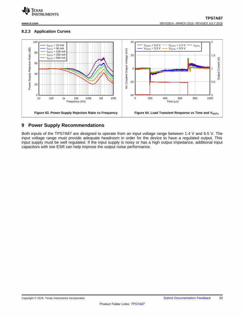
Frequency (Hz)
Pow
er-S
uppl
y R
ejec
tion
Rat
io (
dB)
0
20
40
60
80
100
10 100 1k 10k 100k 1M 10M
IOUTx = 10 mAIOUTx = 50 mAIOUTx = 100 mAIOUTx = 250 mAIOUTx = 500 mA
Time (Ps)
AC
-Cou
pled
Out
put V
olta
ge (
mV
)
Out
put C
urre
nt (
A)
0 200 400 600 800 1000-50 0
-25 0.5
0 1
25 1.5
50 2VOUTx = 5.0 VVOUTx = 3.3 V
VOUTx = 1.2 VVOUTx = 0.9 V
IOUTx
33
TPS7A87www.ti.com SBVS281A –MARCH 2016–REVISED JULY 2016
Product Folder Links: TPS7A87
Submit Documentation FeedbackCopyright © 2016, Texas Instruments Incorporated
8.2.3 Application Curves
Figure 63. Power-Supply Rejection Ratio vs Frequency Figure 64. Load Transient Response vs Time and VOUTx
9 Power Supply RecommendationsBoth inputs of the TPS7A87 are designed to operate from an input voltage range between 1.4 V and 6.5 V. Theinput voltage range must provide adequate headroom in order for the device to have a regulated output. Thisinput supply must be well regulated. If the input supply is noisy or has a high output impedance, additional inputcapacitors with low ESR can help improve the output noise performance.
34
TPS7A87SBVS281A –MARCH 2016–REVISED JULY 2016 www.ti.com
Product Folder Links: TPS7A87
Submit Documentation Feedback Copyright © 2016, Texas Instruments Incorporated
10 Layout
10.1 Layout GuidelinesGeneral guidelines for linear regulator designs are to place all circuit components on the same side of the circuitboard and as near as practical to the respective LDO pin connections. Place ground return connections to theinput and output capacitor, and to the LDO ground pin as close to each other as possible, connected by a wide,component-side, copper surface. The use of vias and long traces to create LDO circuit connections is stronglydiscouraged and negatively affects system performance.
10.1.1 Board LayoutTo maximize the performance of the device, following the layout example illustrated in Figure 65 isrecommended. This layout isolates the analog ground (AGND) from the noisy power ground. Components thatmust be connected to the quiet analog ground are the noise-reduction capacitors (CNR/SSx) and the lowerfeedback resistors (R2x). These components must have a separate connection back to the thermal pad of thedevice. To minimize crosstalk between the two outputs, the output capacitor grounds are positioned on oppositesides of the layout and only connect back to the device at opposite sides of the thermal pad. Connecting theGND pins directly to the thermal pad and not to any external plane is recommended.
To maximize the output voltage accuracy, the connection from each output voltage back to the top output dividerresistors (R1x) must be made as close as possible to the load. This method of connecting the feedback traceeliminates the voltage drop from the device output to the load.
To improve thermal performance, a 3 × 3 thermal via array must connect the thermal pad to internal groundplanes. A larger area for the internal ground planes improves the thermal performance and lowers the operatingtemperature of the device.

CIN2 COUT2
CNR/SS2
CFF2
R12
R22
RPG2
OUT1
EN
1
IN1
NR
/SS
1
PG
1
FB
1
EN
2
NR
/SS
2
PG
2
FB
2
SS
_CT
RL1
SS
_CT
RL2
OUT2IN2
IN1
IN2
OUT1
OUT2
GND GND
1
5
2
4
3
15
11
14
12
13
6 7 8 9 10
20 19 18 17 16CIN1 COUT1
CNR/SS1
CFF1
R11
R21
RPG1
Thermal Ground
Thermal Ground
AGND
AGND
VIN1
VIN2VOUT2
VOUT1
VOUT1 SENSE on Bottom Layer
VOUT2 SENSE on Bottom Layer
PG1
PG2
Circles denote PCB via connections.
35
TPS7A87www.ti.com SBVS281A –MARCH 2016–REVISED JULY 2016
Product Folder Links: TPS7A87
Submit Documentation FeedbackCopyright © 2016, Texas Instruments Incorporated
10.2 Layout Example
Figure 65. TPS7A87 Example Layout

36
TPS7A87SBVS281A –MARCH 2016–REVISED JULY 2016 www.ti.com
Product Folder Links: TPS7A87
Submit Documentation Feedback Copyright © 2016, Texas Instruments Incorporated
(1) For the most current package and ordering information see the Package Option Addendum at the end of this document, or see thedevice product folder at www.ti.com.
11 Device and Documentation Support
11.1 Device Support
11.1.1 Development Support
11.1.1.1 Evaluation ModulesAn evaluation module (EVM) is available to assist in the initial circuit performance evaluation using the TPS7A87.The summary information for this fixture is shown in Table 11.
Table 11. Design Kits & Evaluation Modules (1)
NAME PART NUMBERTPS7A88 evaluation module TPS7A88EVM User's Guide
(1) For the most current package and ordering information see the Package Option Addendum at the end of this document, or see thedevice product folder at www.ti.com.
The EVM can be requested at the Texas Instruments web site (www.ti.com) through the TPS7A87 product folder.
11.1.1.2 SPICE ModelsComputer simulation of circuit performance using SPICE is often useful when analyzing the performance ofanalog circuits and systems. A SPICE model for the TPS7A87 is available through the TPS7A87 product folderunder simulation models.
11.1.2 Device Nomenclature
Table 12. Ordering Information (1)
PRODUCT DESCRIPTION
TPS7A87XXYYYZXX represents the output voltage. 01 is the adjustable output version.YYY is the package designator.Z is the package quantity.
11.2 Documentation Support
11.2.1 Related DocumentationFor related documentation see the following:• TPS37xx Dual-Channel, Low-Power, High-Accuracy Voltage Detectors Data Sheet (SBVS250)• TPS7A88 Evaluation Module User's Guide (SBVU027)• Pros and Cons of Using a Feed-Forward Capacitor with a Low Dropout Regulator Application Report
(SBVA042)• How to Measure LDO Noise White Paper (SLYY076)
11.3 Receiving Notification of Documentation UpdatesTo receive notification of documentation updates, navigate to the device product folder on ti.com. In the upperright corner, click on Alert me to register and receive a weekly digest of any product information that haschanged. For change details, review the revision history included in any revised document.
37
TPS7A87www.ti.com SBVS281A –MARCH 2016–REVISED JULY 2016
Product Folder Links: TPS7A87
Submit Documentation FeedbackCopyright © 2016, Texas Instruments Incorporated
11.4 Community ResourcesThe following links connect to TI community resources. Linked contents are provided "AS IS" by the respectivecontributors. They do not constitute TI specifications and do not necessarily reflect TI's views; see TI's Terms ofUse.
TI E2E™ Online Community TI's Engineer-to-Engineer (E2E) Community. Created to foster collaborationamong engineers. At e2e.ti.com, you can ask questions, share knowledge, explore ideas and helpsolve problems with fellow engineers.
Design Support TI's Design Support Quickly find helpful E2E forums along with design support tools andcontact information for technical support.
11.5 TrademarksE2E is a trademark of Texas Instruments.All other trademarks are the property of their respective owners.
11.6 Electrostatic Discharge CautionThis integrated circuit can be damaged by ESD. Texas Instruments recommends that all integrated circuits be handled withappropriate precautions. Failure to observe proper handling and installation procedures can cause damage.
ESD damage can range from subtle performance degradation to complete device failure. Precision integrated circuits may be moresusceptible to damage because very small parametric changes could cause the device not to meet its published specifications.
11.7 GlossarySLYZ022 — TI Glossary.
This glossary lists and explains terms, acronyms, and definitions.
12 Mechanical, Packaging, and Orderable InformationThe following pages include mechanical, packaging, and orderable information. This information is the mostcurrent data available for the designated devices. This data is subject to change without notice and revision ofthis document. For browser-based versions of this data sheet, refer to the left-hand navigation.

PACKAGE OPTION ADDENDUM
www.ti.com 31-Jul-2016
Addendum-Page 1
PACKAGING INFORMATION
Orderable Device Status(1)
Package Type PackageDrawing
Pins PackageQty
Eco Plan(2)
Lead/Ball Finish(6)
MSL Peak Temp(3)
Op Temp (°C) Device Marking(4/5)
Samples
TPS7A8701RTJR ACTIVE QFN RTJ 20 3000 Green (RoHS& no Sb/Br)
CU NIPDAU Level-2-260C-1 YEAR -40 to 125 TPS7A87
TPS7A8701RTJT ACTIVE QFN RTJ 20 250 Green (RoHS& no Sb/Br)
CU NIPDAU Level-2-260C-1 YEAR -40 to 125 TPS7A87
(1) The marketing status values are defined as follows:ACTIVE: Product device recommended for new designs.LIFEBUY: TI has announced that the device will be discontinued, and a lifetime-buy period is in effect.NRND: Not recommended for new designs. Device is in production to support existing customers, but TI does not recommend using this part in a new design.PREVIEW: Device has been announced but is not in production. Samples may or may not be available.OBSOLETE: TI has discontinued the production of the device.
(2) Eco Plan - The planned eco-friendly classification: Pb-Free (RoHS), Pb-Free (RoHS Exempt), or Green (RoHS & no Sb/Br) - please check http://www.ti.com/productcontent for the latest availabilityinformation and additional product content details.TBD: The Pb-Free/Green conversion plan has not been defined.Pb-Free (RoHS): TI's terms "Lead-Free" or "Pb-Free" mean semiconductor products that are compatible with the current RoHS requirements for all 6 substances, including the requirement thatlead not exceed 0.1% by weight in homogeneous materials. Where designed to be soldered at high temperatures, TI Pb-Free products are suitable for use in specified lead-free processes.Pb-Free (RoHS Exempt): This component has a RoHS exemption for either 1) lead-based flip-chip solder bumps used between the die and package, or 2) lead-based die adhesive used betweenthe die and leadframe. The component is otherwise considered Pb-Free (RoHS compatible) as defined above.Green (RoHS & no Sb/Br): TI defines "Green" to mean Pb-Free (RoHS compatible), and free of Bromine (Br) and Antimony (Sb) based flame retardants (Br or Sb do not exceed 0.1% by weightin homogeneous material)
(3) MSL, Peak Temp. - The Moisture Sensitivity Level rating according to the JEDEC industry standard classifications, and peak solder temperature.
(4) There may be additional marking, which relates to the logo, the lot trace code information, or the environmental category on the device.
(5) Multiple Device Markings will be inside parentheses. Only one Device Marking contained in parentheses and separated by a "~" will appear on a device. If a line is indented then it is a continuationof the previous line and the two combined represent the entire Device Marking for that device.
(6) Lead/Ball Finish - Orderable Devices may have multiple material finish options. Finish options are separated by a vertical ruled line. Lead/Ball Finish values may wrap to two lines if the finishvalue exceeds the maximum column width.
Important Information and Disclaimer:The information provided on this page represents TI's knowledge and belief as of the date that it is provided. TI bases its knowledge and belief on informationprovided by third parties, and makes no representation or warranty as to the accuracy of such information. Efforts are underway to better integrate information from third parties. TI has taken andcontinues to take reasonable steps to provide representative and accurate information but may not have conducted destructive testing or chemical analysis on incoming materials and chemicals.TI and TI suppliers consider certain information to be proprietary, and thus CAS numbers and other limited information may not be available for release.

PACKAGE OPTION ADDENDUM
www.ti.com 31-Jul-2016
Addendum-Page 2
In no event shall TI's liability arising out of such information exceed the total purchase price of the TI part(s) at issue in this document sold by TI to Customer on an annual basis.

TAPE AND REEL INFORMATION
*All dimensions are nominal
Device PackageType
PackageDrawing
Pins SPQ ReelDiameter
(mm)
ReelWidth
W1 (mm)
A0(mm)
B0(mm)
K0(mm)
P1(mm)
W(mm)
Pin1Quadrant
TPS7A8701RTJR QFN RTJ 20 3000 330.0 12.4 4.25 4.25 1.15 8.0 12.0 Q2
TPS7A8701RTJT QFN RTJ 20 250 180.0 12.4 4.25 4.25 1.15 8.0 12.0 Q2
PACKAGE MATERIALS INFORMATION
www.ti.com 29-Jul-2016
Pack Materials-Page 1

*All dimensions are nominal
Device Package Type Package Drawing Pins SPQ Length (mm) Width (mm) Height (mm)
TPS7A8701RTJR QFN RTJ 20 3000 367.0 367.0 35.0
TPS7A8701RTJT QFN RTJ 20 250 210.0 185.0 35.0
PACKAGE MATERIALS INFORMATION
www.ti.com 29-Jul-2016
Pack Materials-Page 2


IMPORTANT NOTICE
Texas Instruments Incorporated and its subsidiaries (TI) reserve the right to make corrections, enhancements, improvements and otherchanges to its semiconductor products and services per JESD46, latest issue, and to discontinue any product or service per JESD48, latestissue. Buyers should obtain the latest relevant information before placing orders and should verify that such information is current andcomplete. All semiconductor products (also referred to herein as “components”) are sold subject to TI’s terms and conditions of salesupplied at the time of order acknowledgment.TI warrants performance of its components to the specifications applicable at the time of sale, in accordance with the warranty in TI’s termsand conditions of sale of semiconductor products. Testing and other quality control techniques are used to the extent TI deems necessaryto support this warranty. Except where mandated by applicable law, testing of all parameters of each component is not necessarilyperformed.TI assumes no liability for applications assistance or the design of Buyers’ products. Buyers are responsible for their products andapplications using TI components. To minimize the risks associated with Buyers’ products and applications, Buyers should provideadequate design and operating safeguards.TI does not warrant or represent that any license, either express or implied, is granted under any patent right, copyright, mask work right, orother intellectual property right relating to any combination, machine, or process in which TI components or services are used. Informationpublished by TI regarding third-party products or services does not constitute a license to use such products or services or a warranty orendorsement thereof. Use of such information may require a license from a third party under the patents or other intellectual property of thethird party, or a license from TI under the patents or other intellectual property of TI.Reproduction of significant portions of TI information in TI data books or data sheets is permissible only if reproduction is without alterationand is accompanied by all associated warranties, conditions, limitations, and notices. TI is not responsible or liable for such altereddocumentation. Information of third parties may be subject to additional restrictions.Resale of TI components or services with statements different from or beyond the parameters stated by TI for that component or servicevoids all express and any implied warranties for the associated TI component or service and is an unfair and deceptive business practice.TI is not responsible or liable for any such statements.Buyer acknowledges and agrees that it is solely responsible for compliance with all legal, regulatory and safety-related requirementsconcerning its products, and any use of TI components in its applications, notwithstanding any applications-related information or supportthat may be provided by TI. Buyer represents and agrees that it has all the necessary expertise to create and implement safeguards whichanticipate dangerous consequences of failures, monitor failures and their consequences, lessen the likelihood of failures that might causeharm and take appropriate remedial actions. Buyer will fully indemnify TI and its representatives against any damages arising out of the useof any TI components in safety-critical applications.In some cases, TI components may be promoted specifically to facilitate safety-related applications. With such components, TI’s goal is tohelp enable customers to design and create their own end-product solutions that meet applicable functional safety standards andrequirements. Nonetheless, such components are subject to these terms.No TI components are authorized for use in FDA Class III (or similar life-critical medical equipment) unless authorized officers of the partieshave executed a special agreement specifically governing such use.Only those TI components which TI has specifically designated as military grade or “enhanced plastic” are designed and intended for use inmilitary/aerospace applications or environments. Buyer acknowledges and agrees that any military or aerospace use of TI componentswhich have not been so designated is solely at the Buyer's risk, and that Buyer is solely responsible for compliance with all legal andregulatory requirements in connection with such use.TI has specifically designated certain components as meeting ISO/TS16949 requirements, mainly for automotive use. In any case of use ofnon-designated products, TI will not be responsible for any failure to meet ISO/TS16949.
Products ApplicationsAudio www.ti.com/audio Automotive and Transportation www.ti.com/automotiveAmplifiers amplifier.ti.com Communications and Telecom www.ti.com/communicationsData Converters dataconverter.ti.com Computers and Peripherals www.ti.com/computersDLP® Products www.dlp.com Consumer Electronics www.ti.com/consumer-appsDSP dsp.ti.com Energy and Lighting www.ti.com/energyClocks and Timers www.ti.com/clocks Industrial www.ti.com/industrialInterface interface.ti.com Medical www.ti.com/medicalLogic logic.ti.com Security www.ti.com/securityPower Mgmt power.ti.com Space, Avionics and Defense www.ti.com/space-avionics-defenseMicrocontrollers microcontroller.ti.com Video and Imaging www.ti.com/videoRFID www.ti-rfid.comOMAP Applications Processors www.ti.com/omap TI E2E Community e2e.ti.comWireless Connectivity www.ti.com/wirelessconnectivity
Mailing Address: Texas Instruments, Post Office Box 655303, Dallas, Texas 75265Copyright © 2016, Texas Instruments Incorporated