using vcos as rf measuring devices by carl elliot taylor
TRANSCRIPT

USING VCOS AS RF MEASURING DEVICES
by
Carl Elliot Taylor
BS, University of Pittsburgh, 2000
Submitted to the Graduate Faculty of
the University of Pittsburgh in partial fulfillment
of the requirements for the degree of
Master’s of Science in Electrical Engineering
University of Pittsburgh
2004

UNIVERSITY OF PITTSBURGH
SCHOOL OF ENGINEERING
This thesis was presented
by
Carl Elliot Taylor
It was defended on
August 4th, 2003
and approved by
James T. Cain, Assistant Professor, Electrical Engineering Department
Raymond R. Hoare, Assistant Professor, Electrical Engineering Department
Ronald G. Hoelzeman, Assistant Professor, Electrical Engineering Department
Thesis Advisor: Marlin H. Mickle, Nickolas A. DeCecco Professor, Electrical Engineering Department
ii
USING VCOS AS RF MEASURING DEVICES
Carl Elliot Taylor, MS
University of Pittsburgh, 2004
This thesis presents an alternative way to test the amount of energy harvested by an antenna.
Accurately measuring the amount of energy an antenna harvests is a challenge. The test
equipment that touches the antenna can greatly affect the results of the test. Using a VCO to
measure an antenna’s harvested power enables accuracy and prevents the need to attach testing
equipment. The VCO is powered by a harvesting antenna. The frequency produced is then
output to a transmitting antenna. The output frequency of the VCO can easily be determined and
then used to look up the power from the characteristics of the VCO. A background study of
types of VCOs, and VCOs available on the market will also be included in this thesis. Finally
the experiment setups and results will be presented.
iii
TABLE OF CONTENTS
1.0 BACKGROUND OF THE PROBLEM.................................................................................... 1
1.1 GENERALITIES .......................................................................................................... 1
1.2 STATEMENT OF THE PROBLEM............................................................................ 2
2.0 ANTENNAS ON-CHIP............................................................................................................ 3
2.1 RF ID TAGS................................................................................................................. 4
2.1.1 On-Chip Solution ........................................................................................... 4
2.1.1.1 Antennas ..................................................................................................... 7
3.0 CURRENT ANTENNA TESTING PROBLEMS.................................................................. 10
3.1 CONNECTED TEST EQUIPMENT.......................................................................... 10
3.2 LED POWER METER ............................................................................................... 11
4.0 BACKGROUND OF A VCO................................................................................................. 14
4.1 VCO DEFINITION .................................................................................................... 14
4.2 TYPES OF VCOS....................................................................................................... 17
4.2.1 LC Oscillators .............................................................................................. 18
4.2.2 Non-LC Oscillators...................................................................................... 19
4.2.2.1 Current Starved Oscillator ........................................................................ 20
4.2.2.2 Interpolation.............................................................................................. 23
4.2.3 Special Components..................................................................................... 24
4.2.3.1 Tunable Capacitors ................................................................................... 25
4.2.3.2 Tunable Diode........................................................................................... 29
4.2.3.3 Varactor Transistors.................................................................................. 30
5.0 CURRENT VCO USES.......................................................................................................... 35
5.1 PHASE LOCK LOOPS .............................................................................................. 35
6.0 THE VCO SOLUTION .......................................................................................................... 37
7.0 ANALOG SUPPORT CIRCUITRY....................................................................................... 38
iv

7.1 SPIRAL DELTA ANTENNA .................................................................................... 39
7.2 CHARGE PUMP ........................................................................................................ 40
7.3 IMPENDENCE MATCHING .................................................................................... 41
7.4 AMPLIFIER ............................................................................................................... 42
8.0 AVAILABLE TEHCNOLOGIES .......................................................................................... 44
9.0 THE VCO DESIGN AND VERIFICATION EXPERIEMENTS.......................................... 46
9.1 OSCILATOR DESIGN .............................................................................................. 46
9.1.1 Experiment Description ............................................................................... 46
9.1.1.1 Objective ................................................................................................... 46
9.1.1.2 Background Information........................................................................... 47
9.1.1.3 Test Setup.................................................................................................. 51
9.1.2 Results.......................................................................................................... 62
9.1.2.1 VCO 1 Results .......................................................................................... 63
9.2 TRANSMISSION I EXPERIMENT .......................................................................... 67
9.2.1 Description................................................................................................... 67
9.2.1.1 Objective ................................................................................................... 67
9.2.1.2 What was accomplished............................................................................ 68
9.2.1.3 Test Rig Setup........................................................................................... 69
9.2.1.4 Equipment Setup....................................................................................... 72
9.2.2 Results.......................................................................................................... 75
9.3 TRANSMISSION II EXPERIMENT......................................................................... 77
9.3.1 Description................................................................................................... 77
9.3.1.1 Objective ................................................................................................... 77
9.3.1.2 What was accomplished............................................................................ 77
9.3.1.3 Test Rig Setup........................................................................................... 78
10.0 CONCLUSION..................................................................................................................... 81
11.0 CONTRBUTIONS................................................................................................................ 82
APPENDIX A............................................................................................................................... 84
VCO Comparison Test...................................................................................................... 84
11.1 VCO 1 Results .......................................................................................................... 84
11.2 VCO 2 Results .......................................................................................................... 87
v

APENDIX B ................................................................................................................................. 90
Transmission Experiment ................................................................................................. 90
11.3 Transmission Results ................................................................................................ 90
BIBLIOGRAPHY......................................................................................................................... 93
vi
LIST OF TABLES
Table 1. LED Power Look Up Table ............................................................................................ 12
Table 2. VCO1 (digital) Analyzer Results.................................................................................... 64
Table 3. VCO2 (analog) Analyzer Results ................................................................................... 65
Table 4. Transmitted Results Compared to the Non-Transmitted Results ................................... 76
vii

LIST OF FIGURES
Figure 1. E-ZPass Electric Toll Collector....................................................................................... 5
Figure 2. Mobil’s Speedpass ID Tag .............................................................................................. 6
Figure 3. An On-Chip, Self-Contained RF-ID................................................................................ 7
Figure 4. RF-ID Block Diagram ..................................................................................................... 8
Figure 5. LED Power Meter.......................................................................................................... 12
Figure 6. Frequency vs. Voltage of an Ideal VCO ....................................................................... 15
Figure 7. Tuning Non-Linearity.................................................................................................... 17
Figure 8. CMOS oscillator with self-switching inductors ............................................................ 19
Figure 9. Ring Oscillator............................................................................................................... 20
Figure 10. A Full Current Starved VCO....................................................................................... 21
Figure 11. A Simple Current-Starving Circuitry .......................................................................... 22
Figure 12. Current Starved Ring Oscillator .................................................................................. 23
Figure 13. Interpolation Node Ring .............................................................................................. 23
Figure 14. Interpolation Node....................................................................................................... 24
Figure 15. A Simplified Colpitts Oscillator.................................................................................. 25
Figure 16. A Negative Resistance LC Oscillator.......................................................................... 26
Figure 17. Varactor Capacitor Conceptual ................................................................................... 27
Figure 18. Varactor Capacitor Profile........................................................................................... 28
Figure 19. VCO Containing Varactor Capacitors......................................................................... 29
Figure 20. Topology of VCO with a Tunable Diode .................................................................... 30
Figure 21. VCO with PMOS Capacitors....................................................................................... 31
Figure 22. Varactor Transistor with B = D = S ............................................................................ 32
Figure 23. An A-MOS Varactor Transistor Profile ...................................................................... 33
Figure 24. A-MOS vs. B=D=S ..................................................................................................... 33
Figure 25. Phase-Locked-Loop Block Diagram ........................................................................... 36
viii

Figure 26. Support Circuitry Flow Chart...................................................................................... 39
Figure 27. The Spiral Delta Antenna ............................................................................................ 40
Figure 28. Voltage Doubler .......................................................................................................... 41
Figure 29. Voltage Doubler Layout .............................................................................................. 41
Figure 30. A Simple π Matching Network.................................................................................. 42
Figure 31. Low Noise Amplifier................................................................................................... 43
Figure 32. Current Starved Oscillator with Sizes ......................................................................... 49
Figure 33. APLAC’s Oscillation Simulator.................................................................................. 50
Figure 34. Ansoft’s Oscillator Simulator...................................................................................... 51
Figure 35. VCO Chip with the Patch Antennas............................................................................ 52
Figure 36. Example of a Circuit Using a Mirroring Technique.................................................... 53
Figure 37. Dummy elements outside of the protected elements................................................... 54
Figure 38. An example of using unit sizes.................................................................................... 54
Figure 39. An example of a guard ring ......................................................................................... 55
Figure 40. An example of a capacitor using the finger technique ................................................ 56
Figure 41. Digital Style VCO layout (VCO1) .............................................................................. 57
Figure 42. Analog Style VCO layout (VCO2).............................................................................. 58
Figure 43. The VCO Test Rig....................................................................................................... 59
Figure 44. Theta Wire Bonds........................................................................................................ 60
Figure 45. Pomona 3073 Power Adaptor...................................................................................... 61
Figure 46. Power Supply............................................................................................................... 61
Figure 47. VCO Test Setup........................................................................................................... 62
Figure 48. VCO1 and VCO2 Frequency vs. Voltage ................................................................... 66
Figure 49. VCO1 and VCO2 dBm vs. Voltage ............................................................................ 66
Figure 50. Theta chip .................................................................................................................... 69
Figure 51. Epsilon Chip ................................................................................................................ 70
Figure 52. Test Rig ....................................................................................................................... 71
Figure 53. Bonding Diagram of Transmission Experiment.......................................................... 72
Figure 54. Test Equipment............................................................................................................ 73
Figure 55. Maxrad 900 MHz antenna ........................................................................................... 73
Figure 56. Spectrum Analyzer, Test Rig and Receiving Antenna................................................ 74
ix
Figure 57. Transmit I Test Setup .................................................................................................. 75
Figure 58. Transmitted I Compared to Non-Transmitted Results ................................................ 76
Figure 59. Iota Chip ...................................................................................................................... 78
Figure 60. Bonding Diagram of Transmission II Experiment ...................................................... 79
Figure 61. Transmitting II Test Setup........................................................................................... 80
Figure 62. VCO 1 Analyzer Results: 1.5 Volts and 2.0 Volts ...................................................... 84
Figure 63. VCO 1 Analyzer Results: 2.5 Volts and 3 Volts ......................................................... 85
Figure 64. VCO 1 Analyzer Results: 3.5 Volts and 4 Volts ......................................................... 85
Figure 65. VCO 1 Analyzer Results: 4.5 Volts and 5 Volts ......................................................... 86
Figure 66. VCO 1 Analyzer Results: 5.5 Volts and 6 Volts ......................................................... 86
Figure 67. VCO 2 Analyzer Results: 1.5 Volts and 2 Volts ......................................................... 87
Figure 68. VCO 2 Analyzer Results: 2.5 Volts and 3 Volts ......................................................... 87
Figure 69. VCO 2 Analyzer Results: 3.5 Volts and 4 Volts ......................................................... 88
Figure 70. VCO 2 Analyzer Results: 4.5 Volts and 5 Volts ......................................................... 88
Figure 71. VCO 2 Analyzer Results: 5.5 Volts and 6 Volts ........................................................ 89
Figure 72. Transmitted Analyzer Results: 2.5 Volts and 3 Volts ................................................ 90
Figure 73. Transmitted Analyzer Results: 3.5 Volts and 4 Volts ................................................ 91
Figure 74. Transmitted Analyzer Results: 4.5 Volts and 5 Volts ................................................ 91
Figure 75. Transmitted Analyzer Results: 5.5 Volts and 6 Volts ................................................ 92
x

ACKNOWLEDGEMENTS
First of all I would like to thank Dr. Marlin Mickle for his support and guidance. He has been a
big part of my success with my experiments, my thesis, and mentoring me. I would like to thank
Dr. Thomas Cain, Dr. Ronald Hoelzeman, and Dr. Hoare for their advice and sitting on my thesis
committee. I would like to thank Dr. Minhong Mi for his information on the voltage doubler. I
would like to thank Charlie Greene for his advice on the impedance matching. I would also like
to thank Dr. Frank Herzel who was very helpful when I requested more details about a VCO that
was in one of his papers [1].
xi

1.0 BACKGROUND OF THE PROBLEM
1.1 GENERALITIES
Wireless electronic devices continue to become smaller and smaller. As this transition of design
and development progress, it becomes more and more difficult to fabricate and test these
prototype wireless devices and their chip (die) implementations. Any physical connection to the
device under test (DUT) tends to distort the RF profile of the DUT.
While many proposed techniques may solve problems of this type, for example, simulation, the
critical questions of the functionality can only be answered by building a prototype of the device.
The solution for the wireless prototype is to fabricate an integral wireless element(s) that will
transmit various parameter measurements as data on a wireless communication link. There are
various technologies such as radio frequency (RF) and infrared (IR) to facilitate the wireless
transmission.
This thesis primarily focuses on research to implement a parametric data link using RF. In the
category of RF, the link will transmit coded data through modulating a carrier frequency, varying
the frequency to denote parametric values of voltage that can provide energy and power.
The designing of the CMOS devices and implementing a wireless link that uses frequency as the
basis for transmitting parameter values will also be the focus of this thesis. The parameter
measurements will be in the terms of DC voltages, and the transducer (voltage to frequency) will
be a voltage controlled oscillator (VCO).
1

1.2 STATEMENT OF THE PROBLEM
The problem to be solved is the design, testing and evaluation of a voltage controlled oscillator
(VCO) in CMOS for use in the measurement of power harvested on autonomous operating
without batteries and wireless chips. The research will consider alternative topologies and
CMOS layouts. The VCO will be tested by transmission through an antenna to a receiving
antenna connected to a spectrum analyzer. The context and basis for the evaluation of alternative
VCO implementations will also be presented.
2

2.0 ANTENNAS ON-CHIP
An emerging field that has sparked the interest of many is the study of on-chip antennas. Until
recently radio frequency (RF) transmissions have been limited to macro antenna designs, which
are on the order of several square inches. The ability to make an antenna of the micro size is
extremely valuable due to reductions in cost and the method of attaching the antenna to products.
There are many uses for such a device.
The current commercial antennas are not on the same chip with the rest of the circuitry and
require wire bonding or other methods of precision attachment. This is an expensive, time
consuming step in manufacturing. Having an antenna on the chip reduces the cost of the circuit
drastically. It can also be fabricated at the same time with the other devices on the chip.
Isolating a circuit from the outside environment is another growing interest. A chip that does not
need batteries or wires attached to it makes this possible. This enables it to be used in
environments where outside bacteria or particles must not come in contact with it. It also can be
embedded making wireless communication possible in demanding environments.
The market for an on-chip antenna is overwhelming. The number of applications is too large to
determine based on current concepts. The most popular application is an identification tag. The
tags can be used to track anything from products in a warehouse to instruments in an emergency
room.
3

2.1 RF ID TAGS
An RFID tag is the fundamental device in an identification technology based on electronic
waves. It has an advantage over the bar code system because no contact or orientation is needed,
it can read and store data, and it can achieve a large amount of information capacity [18].
The potential for affordable RFID tags is enormous. They can revolutionize many industries. A
few of the industries that it would greatly affected by the tags is the retail market, Electric Toll
Collection (ETC), medical, and warehouse inventory.
Shopping markets as well as other retail stores can use the tag instead of a traditional bar code.
The tag would speed shopping checkout lines drastically. It would also allow automatic
inventory updates. A product can be tracked from its creation, to the warehouse, to the
unloading from the truck, to the shelf on the store, and through the checkout as well as providing
a capability for essentially instant inventory.
An example of the potential of an RFID tag is the current ETC system, E-ZPass. E-ZPass, an
electronic toll payment system, is available in many north eastern states. This lowers the number
of toll attendants required, and greatly speeds up the flow of traffic.
The tags also improve automatic payment systems like Mobil’s Speedpass. The tag is about an
inch long and is worn on a key ring. This tag makes it fast and convenient to pay for your gas
without having to go inside or having to insert a credit card into the machine. This technology
can also be extended to parking meters, or any other type of purchase.
2.1.1 On-Chip Solution
In order for RFID tags replace the bar code and become the retail standard, the manufacturing
cost of the tags must be greatly reduced. There are two changes that can take place to make the
4

tags affordable. The antennas can be placed on the chip with the rest of the circuitry, and the
size of the tag needs to be greatly reduced.
A self-contained chip would exhibit the largest reduction in cost. The key to a self-contained
chip is to have multiple antennas on the tag. These antennas are used for harvesting energy and
transmitting the identification information.
Reducing the size of the chip is the next challenge. The smaller the design, the more chips that
can be produced from a single fabrication run. As the number of chips produced on a single run
increases, the price of the chips decreases. This is essential to get an ID tag down to the
“ultimate” target price of 1 cent.
E-ZPass devices for example are the size of a cassette tape. These tags are free to the user, but
cost the E-ZPass service roughly $2.00 to manufacture [20]. The tags could cost less than 10
cents. The savings in the tag production could be passed on to the customers or improving the
road system. Figure 1 is a picture of the current E-ZPass tag.
Figure 1. E-ZPass Electric Toll Collector
5
The cost of the current tags, like Speedpass, is roughly 75 cents or more. Inside the tag’s casing
is an antenna, a chip containing identification information and wire that connects them. The
antenna and the chip can be manufactured inexpensively, but the process required to connect
them is costly and time consuming. That is the most expensive step of the process.
Having a self-contained, on-chip solution cuts the cost to a fraction. The antennas can be on the
chip with the identification hardware. This step will drastically reduce the size of the tag, and
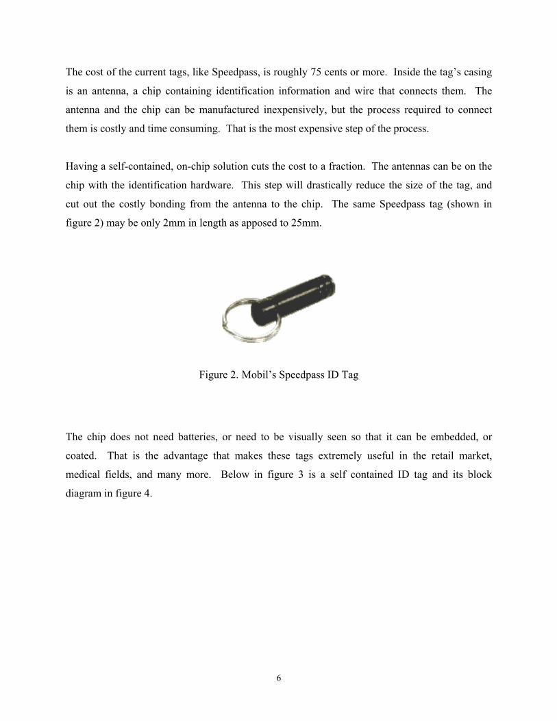
cut out the costly bonding from the antenna to the chip. The same Speedpass tag (shown in
figure 2) may be only 2mm in length as apposed to 25mm.
Figure 2. Mobil’s Speedpass ID Tag
The chip does not need batteries, or need to be visually seen so that it can be embedded, or
coated. That is the advantage that makes these tags extremely useful in the retail market,
medical fields, and many more. Below in figure 3 is a self contained ID tag and its block
diagram in figure 4.
6
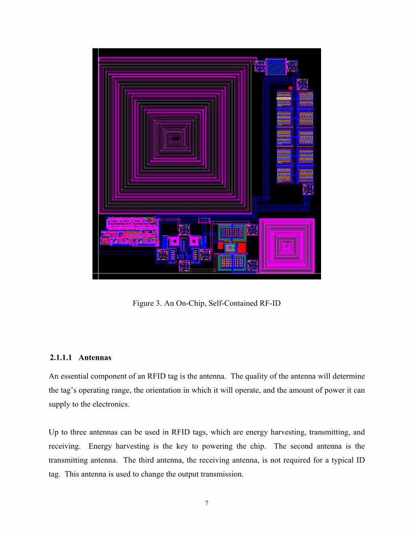
Figure 3. An On-Chip, Self-Contained RF-ID
2.1.1.1 Antennas
An essential component of an RFID tag is the antenna. The quality of the antenna will determine
the tag’s operating range, the orientation in which it will operate, and the amount of power it can
supply to the electronics.
Up to three antennas can be used in RFID tags, which are energy harvesting, transmitting, and
receiving. Energy harvesting is the key to powering the chip. The second antenna is the
transmitting antenna. The third antenna, the receiving antenna, is not required for a typical ID
tag. This antenna is used to change the output transmission.
7
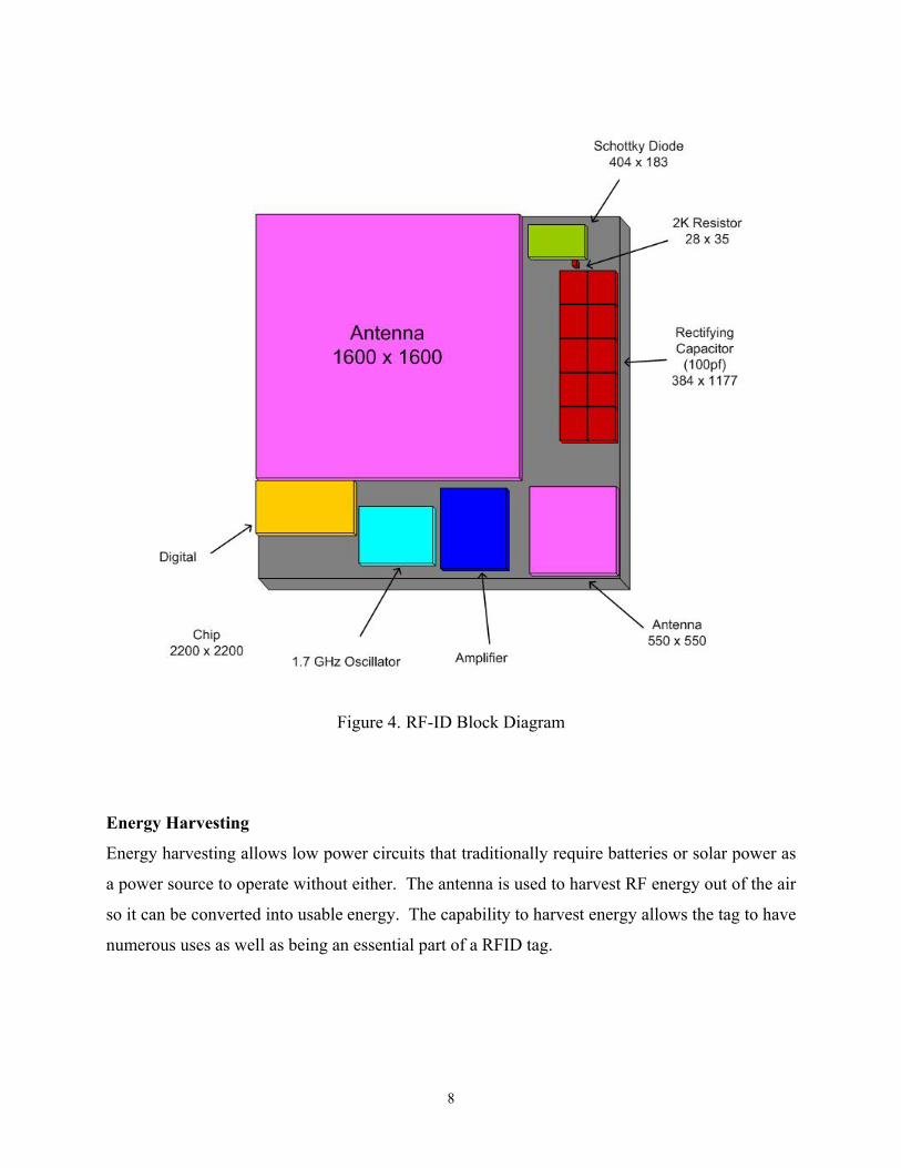
Figure 4. RF-ID Block Diagram
Energy Harvesting
Energy harvesting allows low power circuits that traditionally require batteries or solar power as
a power source to operate without either. The antenna is used to harvest RF energy out of the air
so it can be converted into usable energy. The capability to harvest energy allows the tag to have
numerous uses as well as being an essential part of a RFID tag.
8

Transmitting
The transmitting antenna sends the tag’s identification to a receiving device. This antenna is
typically tuned to a different frequency than the energy harvesting and receiving antennas. The
transmitting antenna input voltage signal must typically be amplified. The quality of the antenna
and the matching network determines the transmitted signal strength. Strong signal strength can
help reduce the cost of the reading equipment.
Receiving
An additional receiving antenna can be used to select multiple outputs. Two outputs can be
hard-coded on the chip and the receiving antenna would select one of the two. The third antenna
can also be used to program the chip. A series of bits can be sent to the chip through the antenna
and stored. When the chip is activated, the stored bits are transmitted.
Having multiple antennas on the same chip complicates the design and testing drastically. Each
antenna must operate at a different frequency. The different frequencies on a single chip can
cause unwanted noise, which can affect the efficiency of the other antennas. Also, the goal is to
reduce the size of the chip and adding another antenna will make it much larger. Therefore
designs that require a third antenna are avoided if possible.
9
3.0 CURRENT ANTENNA TESTING PROBLEMS
The increasing demand for on-chip antennas is alarming. The design of antennas is very
challenging due to the complexity of antenna theory and the effect the surrounding environment
has on an antenna. Moving to the micro size when designing antennas on chips is even more
challenging. The parasitics from the other devices that are also on the chip affect an antenna’s
behavior as well as the chip’s environment.
Testing an antenna’s efficiency has been a major hurdle in their development. When test
equipment is connected to the antenna the equipment can become an antenna itself.
Differentiating the antenna and surrounding circuitry can become extremely involved. A
convenient method of testing is needed that does not touch the actual chip.
3.1 CONNECTED TEST EQUIPMENT
The traditional method of testing an energy harvesting antenna is to expose it to RF energy and
to measure the results with a connected oscilloscope, while shielding the wire as much as
possible.
This method typically involves wire bonding the output of the antenna to typically an SMA
connector, and connecting coaxial cable, which is attached to say a spectrum analyzer. This
solution causes three major problems. The first problem is the coaxial cable can inject noise, or
feedback into the circuit, which may be difficult to determine.
10

The second problem is the connecting cable, as well as the wire bond can become an antenna. It
is not possible to shield the wire bond, and even with the cable shielding the RF waves can
bounce around the shield and contaminate the results.
The third problem is that the wire attached to the chip may make it hard to change the orientation
of the chip to check transmission at different angles. The current primarily purpose of the chip is
to replace the bar code. Therefore the chip must be able to transmit and receive in any
orientation. The ability to test without the test equipment being required to touch the chip will
greatly simplify this task.
3.2 LED POWER METER
Another one of the previous methods that we used to test energy harvesting antennas was the
LED power meter. The power meter is also not very practical for testing on-chip antennas and
was not precise. The LED power meter (figure 5) uses LEDs to estimate the amount of power
the antenna is harvesting. The columns of lights illuminated indicates different amount of
voltage and the intensity indicates the amount of power harvested. Table 1 lists the LEDs
corresponding to a given voltage.
11

Figure 5. LED Power Meter
Table 1. LED Power Look Up Table
LED Power Meter
Column Voltage (V) Power (mW)
One: 1.8 0.09
Two: 3.5 4.03
Three: 5.3 18.23
Four: 7.0 46.40
Five: 8.8 97.42
all LED’s: 12.0 252.00
12
The key reason for the lack of precision of the LED Power Meter is not being able to determine
intermediate voltages when certain LEDs are illuminated. The LED may receive a current
insufficient to completely illuminate it. Determining which LEDs are completely lit and which
LEDs are partially lit becomes difficult. Therefore, the amount of illumination must be
estimated, and the power corresponding to partially illuminated LED must also be estimated.
This problem was the reason for a need for an alternative method of antenna testing. In addition,
this method was used for printed circuit boards (PCB) implementations and is not practical for
CMOS chip fabrications.
13

4.0 BACKGROUND OF A VCO
Before the new method of testing antennas is discussed, some background information on
Voltage Controlled Oscillators (VCOs) is necessary. As well as giving a brief description of
what a VCO is, a number of topologies will be presented along with their advantages and
disadvantages.
4.1 VCO DEFINITION
A Voltage Controlled Oscillator (VCO) is a device that produces alternating current whose
frequency varies as a function of a DC voltage or current. The output frequency is altered by
changing the control voltage or current. An ideal VCO has a linear change in the output
frequency as the voltage changes linearly.
The gain ( ) or sensitivity of a VCO is defined in equation 1.1. The gain is the slope of the
frequency change over the voltage change [3].
vcoK
max min
max minvco
f fK V V=−− (Equation 1.1)
The output frequency of a VCO is noted as ωout, which is defined in equation 1.2. V is the
control voltage, and ω
cont
0 is the frequency when the control voltage is zero (if an oscillation is still
possible at zero). Figure 6 visually defines both , ωvcoK 0 and ωout.
14

contvcooout VK ⋅+=ωω (Equation 1.2)
Figure 6. Frequency vs. Voltage of an Ideal VCO
The different performance parameters that distinguish one VCO from another are the following:
center frequency, tuning range, lock range, tuning linearity, output amplitude, power dissipation,
and signal output noise.
The center frequency ( cω ) is the frequency in the middle of the maximum and minimum
frequencies of the VCO, as shown in equation 1.3. 2ω is the highest frequency and 1ω is the
lowest frequency at which the VCO will oscillate. The operating temperature will also affect the
center frequency [3].
212 ωωω −
=c (Equation 1.3)
15
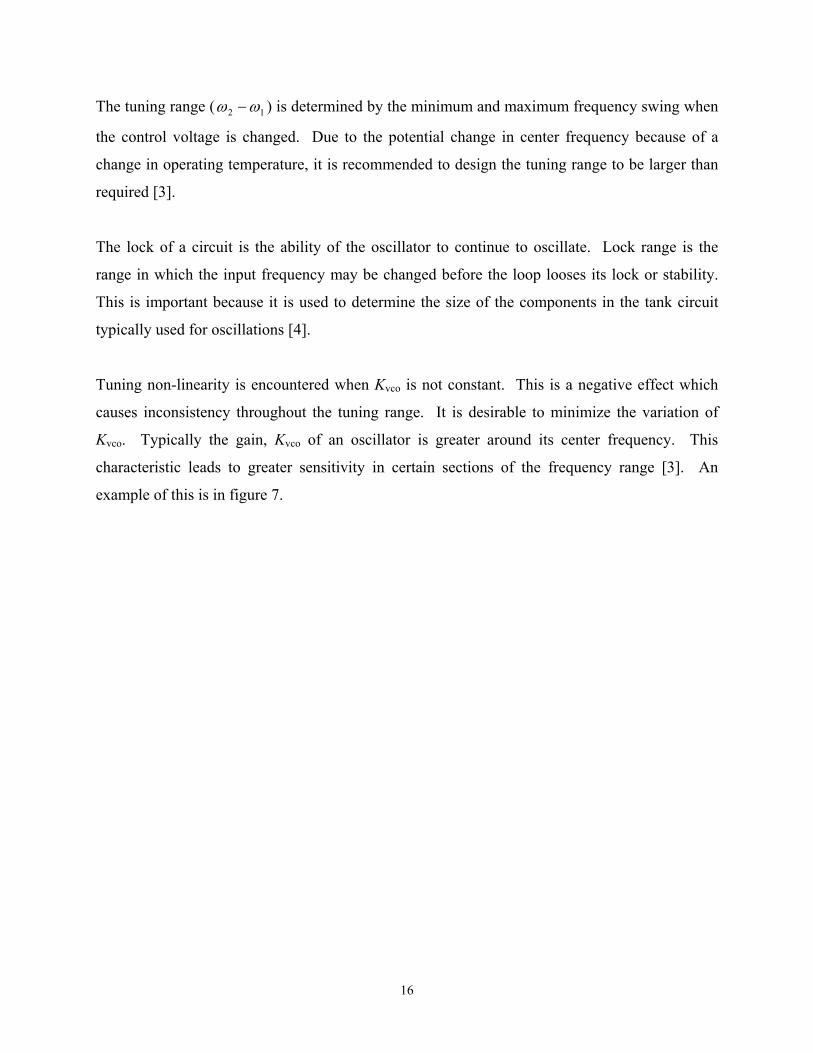
The tuning range ( 12 ωω − ) is determined by the minimum and maximum frequency swing when
the control voltage is changed. Due to the potential change in center frequency because of a
change in operating temperature, it is recommended to design the tuning range to be larger than
required [3].
The lock of a circuit is the ability of the oscillator to continue to oscillate. Lock range is the
range in which the input frequency may be changed before the loop looses its lock or stability.
This is important because it is used to determine the size of the components in the tank circuit
typically used for oscillations [4].
Tuning non-linearity is encountered when Kvco is not constant. This is a negative effect which
causes inconsistency throughout the tuning range. It is desirable to minimize the variation of
Kvco. Typically the gain, Kvco of an oscillator is greater around its center frequency. This
characteristic leads to greater sensitivity in certain sections of the frequency range [3]. An
example of this is in figure 7.
16

Vcont
outω
Figure 7. Tuning Non-Linearity
The output signal quality is the signal to noise ratio. It also is the quality of the actual
oscillation. The quality of the oscillation is the consistency of the oscillation at a given
frequency. Even with a consistent control voltage the oscillation frequency can vary. The noise
of the components in the oscillator can cause these effects. Components with high Q values are
required to raise the signal to noise ratio, and the quality of the overall oscillation.
4.2 TYPES OF VCOS
There are typically three types of voltage controlled oscillators; (1) the traditional
(inductor/capacitance) LC oscillator, (2) the non-LC oscillator, and (3) oscillators containing
special components making variable oscillation possible. The two oscillators with the special
components discussed in this thesis contain electromechanically tunable capacitors, and MOS
varactor transistors.
17

4.2.1 LC Oscillators
The traditional LC VCOs are the most popular for a number of reasons. They do not require a
special, expensive fabrication process, unlike some of the electromechanically tunable capacitors
or varactor transistors. The signal to noise ratio is typically higher than that of a phase lock loop.
The Q values achieved by LC oscillators are superior to the other types of oscillators in the
quality for the amount of design effort and cost of fabrication. They also do not require an
external clock signal.
The oscillation is created from negative feedback which causes the circuit to be unstable. The
instability eventually causes a phase shift. When the Vcont is changed on a traditional VCO the
amount of negative feedback is proportionally changed. The result is an output frequency that
varies [6]. The tuning range is typically smaller compared to the other types of oscillators.
Efforts have been directed towards improving the width of the tuning ranges without having to
use varactor elements or non-LC circuitry. Using inductors in parallel can achieve both high Q
values, and wide tuning ranges, like the circuit in figure 8. Transistors M1 and M2 when turned
on cause L1 and L2 to be in parallel, which lowers the inductance of the tank. The result of the
inductance being lower is the frequency is high. When Vcont is lowered, the current through L2 is
lowered, therefore lowering its inductance. Vcont eventually reaches zero and all of the current
flows through L1 [23]. The inductance across L1 is increased and the frequency will decrease.
18

Figure 8. CMOS oscillator with self-switching inductors
4.2.2 Non-LC Oscillators
The non-LC oscillators have characteristics similar to a digital circuit. They behave like an
analog circuit, but have similar characteristics to that of a digital design. There are two types of
non-LC VCOs. The first is the current starved oscillator, and the second is a technique called
interpolation.
The advantage of the non-LC Oscillators is their wide tuning range. Their tuning range can be as
large as three times the tuning range of the LC VCOs. They also are easy to design. These two
properties make them popular. The disadvantage the non-LC oscillators have is the relatively
high phase noise. This is due to the circuit not containing any passive resonant elements [21].
19
4.2.2.1 Current Starved Oscillator
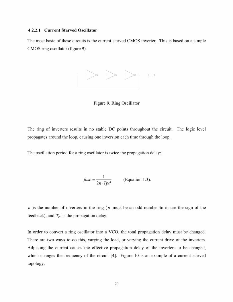
The most basic of these circuits is the current-starved CMOS inverter. This is based on a simple
CMOS ring oscillator (figure 9).
Figure 9. Ring Oscillator
The ring of inverters results in no stable DC points throughout the circuit. The logic level
propagates around the loop, causing one inversion each time through the loop.
The oscillation period for a ring oscillator is twice the propagation delay:
Tpdnfosc
⋅=
21 (Equation 1.3).
n is the number of inverters in the ring ( must be an odd number to insure the sign of the
feedback), and T is the propagation delay.
n
pd
In order to convert a ring oscillator into a VCO, the total propagation delay must be changed.
There are two ways to do this, varying the load, or varying the current drive of the inverters.
Adjusting the current causes the effective propagation delay of the inverters to be changed,
which changes the frequency of the circuit [4]. Figure 10 is an example of a current starved
topology.
20
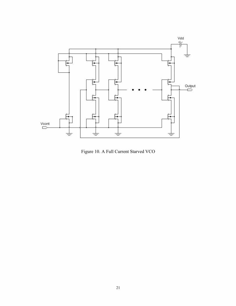
Figure 10. A Full Current Starved VCO
21
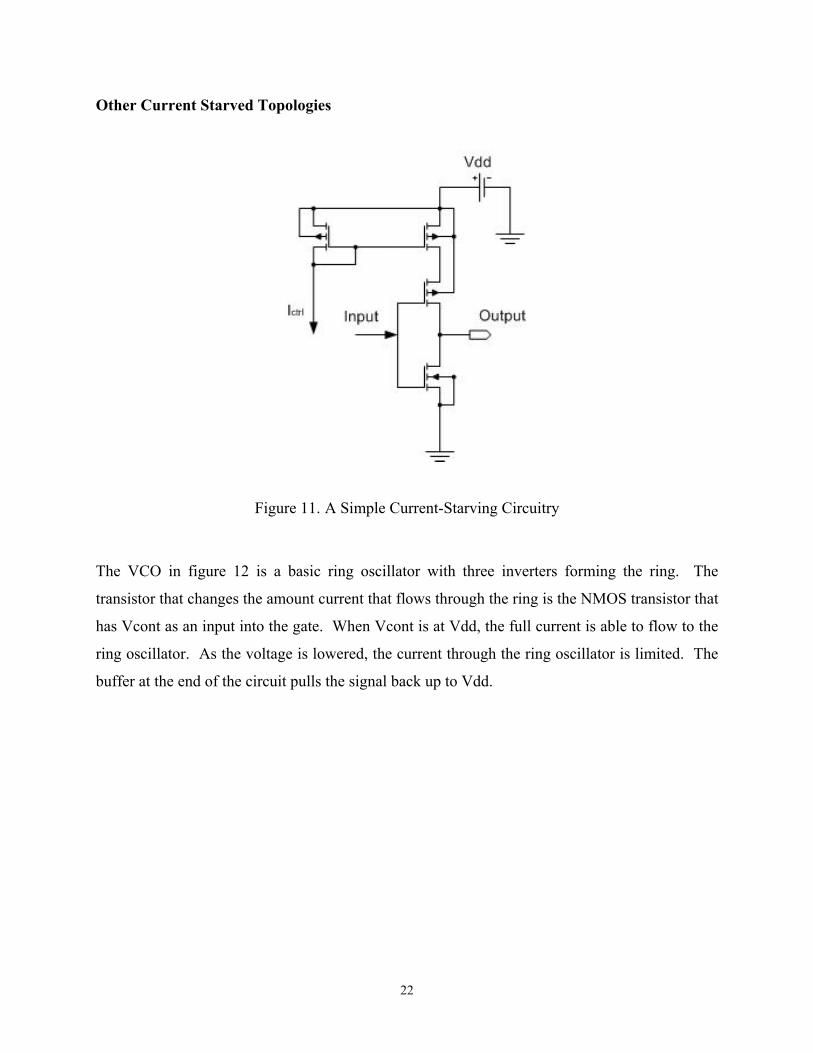
Other Current Starved Topologies
Figure 11. A Simple Current-Starving Circuitry
The VCO in figure 12 is a basic ring oscillator with three inverters forming the ring. The
transistor that changes the amount current that flows through the ring is the NMOS transistor that
has Vcont as an input into the gate. When Vcont is at Vdd, the full current is able to flow to the
ring oscillator. As the voltage is lowered, the current through the ring oscillator is limited. The
buffer at the end of the circuit pulls the signal back up to Vdd.
22

Figure 12. Current Starved Ring Oscillator
4.2.2.2 Interpolation
Another technique to tune ring oscillators is interpolation. Simple adjustable nodes are inserted
into a traditional ring oscillator to accomplish this (figure 13).
Figure 13. Interpolation Node Ring
23

The node (figure 14) has two tracks in which the current can follow. The control voltage Vcont
turns each track on and off. The node is a current adder, which can just be a basic current mirror.
A current mirror is based on copying a current from a reference. That requires that a precisely
defined current source is already available [3].
Figure 14. Interpolation Node
4.2.3 Special Components
Another method of creating a VCO is to use a traditional oscillator topology and electrically alter
the properties of the components. This technique makes it possible to build a complex circuit
with a simple topology. It also has the capability of producing extremely high Q values.
The special components often require special fabrication processes or post-fabrication
alterations. Some however do not require a special fabrication process, but do require changes to
the technology files of the CAD tools. The CAD tools prevent certain masks from being placed
near or on other masks assuming that the user has made an error. Turning off those errors makes
it possible to create some of these components in a traditional CMOS process.
24

4.2.3.1 Tunable Capacitors
A traditional oscillator that contains micromachined electromechanically tunable capacitors is a
new, experimental type of VCO. The tunable capacitors are an integral part of this design. A
VCO can be realized from the very basic oscillator topologies. One of the most basic topologies
is the Colpitts oscillator in figure 15.
Figure 15. A Simplified Colpitts Oscillator
The frequency of a traditional Colpitts LC oscillator is:
1fLC
= (Equation 1.4).
Another popular, simple topology is the negative resistance LC oscillator, which is shown in
figure 16. The negative resistance that is formed in the tank makes this topology popular. The
negative resistance guarantees an oscillation will occur when noise is injected into the circuit.
Tapped resonators are added to a basic negative resistance LC oscillator to achieve signal
amplitudes above the available supply or breakdown voltages [4].
25

Figure 16. A Negative Resistance LC Oscillator
The equation for the fundamental frequency of the negative resistance oscillator is:
12
fLCπ
= (Equation 1.5).
The ability to dynamically change the properties of the components makes the design of the
VCO simple. The inductor and the capacitor are the two components that affect the frequency of
the VCO. Due to the difficulty of changing the inductance of an inductor, most VCO designs
involve changing the capacitance of a capacitor.
There are many experimental techniques being used to electromechanically change the
capacitance. Other devices such as diodes and transistors can change the capacitance of the
26
circuit. There are piezoelectric devices that physically move the plates to create different
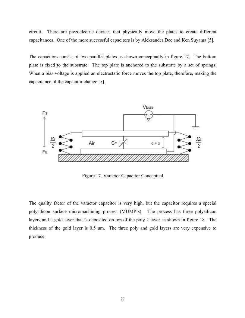
capacitances. One of the more successful capacitors is by Aleksander Dec and Ken Suyama [5].
The capacitors consist of two parallel plates as shown conceptually in figure 17. The bottom
plate is fixed to the substrate. The top plate is anchored to the substrate by a set of springs.
When a bias voltage is applied an electrostatic force moves the top plate, therefore, making the
capacitance of the capacitor change [5].
Figure 17. Varactor Capacitor Conceptual
The quality factor of the varactor capacitor is very high, but the capacitor requires a special
polysilicon surface micromachining process (MUMP’s). The process has three polysilicon
layers and a gold layer that is deposited on top of the poly 2 layer as shown in figure 18. The
thickness of the gold layer is 0.5 um. The three poly and gold layers are very expensive to
produce.
27
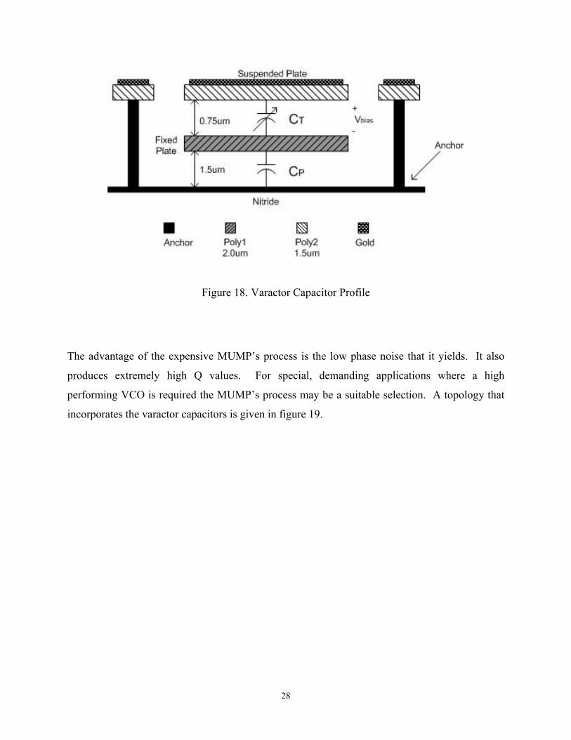
Figure 18. Varactor Capacitor Profile
The advantage of the expensive MUMP’s process is the low phase noise that it yields. It also
produces extremely high Q values. For special, demanding applications where a high
performing VCO is required the MUMP’s process may be a suitable selection. A topology that
incorporates the varactor capacitors is given in figure 19.
28

Figure 19. VCO Containing Varactor Capacitors
4.2.3.2 Tunable Diode
A tunable diode is most widely used to electrically alter properties of an oscillator. The varactor
diode realizes the voltage-variable capacitance [32]. The LC tank is formed by a regular
inductor and the varactor diode. When the control voltage is altered on the anode, the amount of
capacitance between the anode and cathode is also altered. A topology of a VCO containing a
varactor diode is given in figure 20.
29

Figure 20. Topology of VCO with a Tunable Diode
4.2.3.3 Varactor Transistors
Another way to dynamically alter the capacitance of a circuit is to use varactor transistors. When
the drain, source, and bulk silicon are connected they realize a MOS capacitor. These
transistors’ performance exceeds that of a VCO tuned by a reverse bias diode varactor.
The PMOS transistors (M5 and M6) replace the capacitors in figure 21. The two PMOS
transistors with their drain and source tied to ground form the capacitor. The circuit still behaves
like a normal LC circuit, but it has the advantage of not having a capacitor. The PMOS
transistors take up less real-estate than the capacitor and produce wider tuning ranges.
30
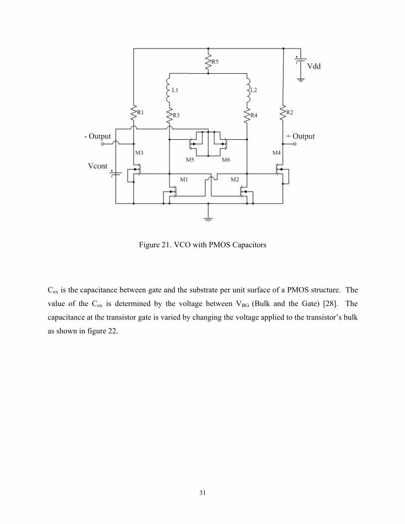
Figure 21. VCO with PMOS Capacitors
Cox is the capacitance between gate and the substrate per unit surface of a PMOS structure. The
value of the Cox is determined by the voltage between VBG (Bulk and the Gate) [28]. The
capacitance at the transistor gate is varied by changing the voltage applied to the transistor’s bulk
as shown in figure 22.
31

Figure 22. Varactor Transistor with B = D = S
Another way to realize a varactor transistor is to limit the transistor to only operate in the
accumulation and depletion modes. This type of transistor is known as an A-MOS transistor.
Preventing the transistor from entering the weak, moderate, and strong inversion modes prevents
the Cmos capacitance from climbing back up to Cox. This is done by preventing any injection of
holes in the MOS channel as shown in figure 23. A way to achieve that condition is by removing
the p+ doping from the MOS device. Figure 24 shows the A-MOS transistor compared to
normal transistor with the bulk, drain, and source tied together (B=D=S).
32
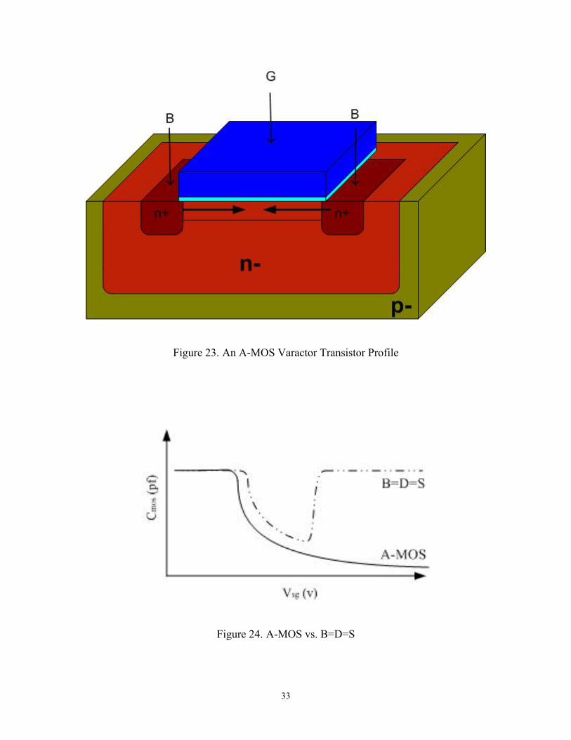
Figure 23. An A-MOS Varactor Transistor Profile
Figure 24. A-MOS vs. B=D=S
33

The A-MOS transistor outperforms the more popular varactor diode and the traditional B=D=S
PMOS as a varactor capacitance. The tuning range of the diode and the A-MOS are both around
11% of the average oscillation frequency, but the A-MOS has lower phase noise [29].
There are other research efforts that are taking place in field of varactor components that are not
mentioned in this thesis. This has been an overview of some of the more recent findings. The
traditional LC circuits are still used more than any other type of VCO. The cost and quality are
usually the reasons for their success. Special applications however do sometimes require special
VCOs.
34

5.0 CURRENT VCO USES
5.1 PHASE LOCK LOOPS
VCOs do not have many traditional uses. They are primarily used in phase lock loops. There
are many uses for a phase lock loop (PPL) circuit. In communications, it readily produces many
frequencies from one reference frequency. They are used in FM and AM radios as
demodulators. They are also used in tone detectors, and frequency synthesizers [11]. In
industrial control applications they are used to control motor speeds.
A phase lock loop is made up of three major components, the phase detector, the loop filter,
amplifier, and a VCO as shown in figure 25. The phase detector compares the phase of an
incoming reference signal with the signal from the VCO, and produces some function of the
phase difference. The loop filter helps eliminate unwanted noise. The amplifier then makes the
signal stronger. The loop filter and amplifier are optional components in a basic PPL. The final
stage is the VCO. The VCO produces the frequency that is a function of the control voltage.
The quality of the VCO determines the necessity of a loop filter and an amplifier.
35

Figure 25. Phase-Locked-Loop Block Diagram
36

6.0 THE VCO SOLUTION
Testing on-chip antennas introduces a non-traditional use of a VCO. It has historically only been
used in phase lock loops, frequency modulation and similar applications. Testing an antenna has
never previously been done by using a VCO as a transducer.
For testing an on-chip antenna, a VCO’s voltage to frequency relationship is required to be
designed, analyzed, and documented. The amount of current the VCO consumes is also
documented. The chip with the antennas under test will consist of an energy harvesting antenna,
a device that converts the harvested RF energy into DC voltage, a VCO, and a transmitting
antenna.
Therefore, when the chip is transmitting an RF signal, the only test equipment that is required is
a spectrum analyzer to act as a receiver with a wide band antenna attached to it. The frequency
received can be recorded and the previously voltage documented can be generated by using a
simple lookup table (Table 2).
The wireless testing of the energy harvesting ability of the antenna also allows the maximum
range of the chip transmission to be tested. The test equipment does not need to be attached to
the chip.
37

7.0 ANALOG SUPPORT CIRCUITRY
Support circuitry as shown in figure 26 is required in order for the VCO to test the antenna’s
efficiency. The harvested energy from the antenna must be converted from RF energy into
usable energy, DC voltage, to power the VCO, by a charge pump. The efficiency of the charge
pump must be very good in order to accurately measure the quality of the antenna. If a high
quality charge pump can not be obtained, then its losses must be predictable.
A matching network between the charge pump and the VCO is necessary for maximum power
transfer. The size of the load of the VCO will also determine the amount of power transferred.
The size of the load and the maximum amount of power transferred are directly proportional.
Another matching network is not necessary, but helpful between the VCO and the Amplifier.
The amplifier boosts the signal from the VCO making the relatively faint signal from the VCO
large enough to be picked up over any ambient RF noise present in the testing environment. The
amplifier must be a wide band to cover the tuning range of the VCO. The center frequency of
the amplifier should be near the center frequency of the VCO.
The amplifier’s output is then sent to the transmitting antenna. The antenna does not need to be
perfectly tuned to transmit the VCOs frequency successfully. It must however be tuned well
enough to transmit a signal that is considerably higher than the noise in the test environment.
The quality of the transmission is not vital because only the frequency is needed. The flow of
the complete circuit can be seen in figure 26. As long as the communications system, path and
channel are linear, the frequency will not change.
38
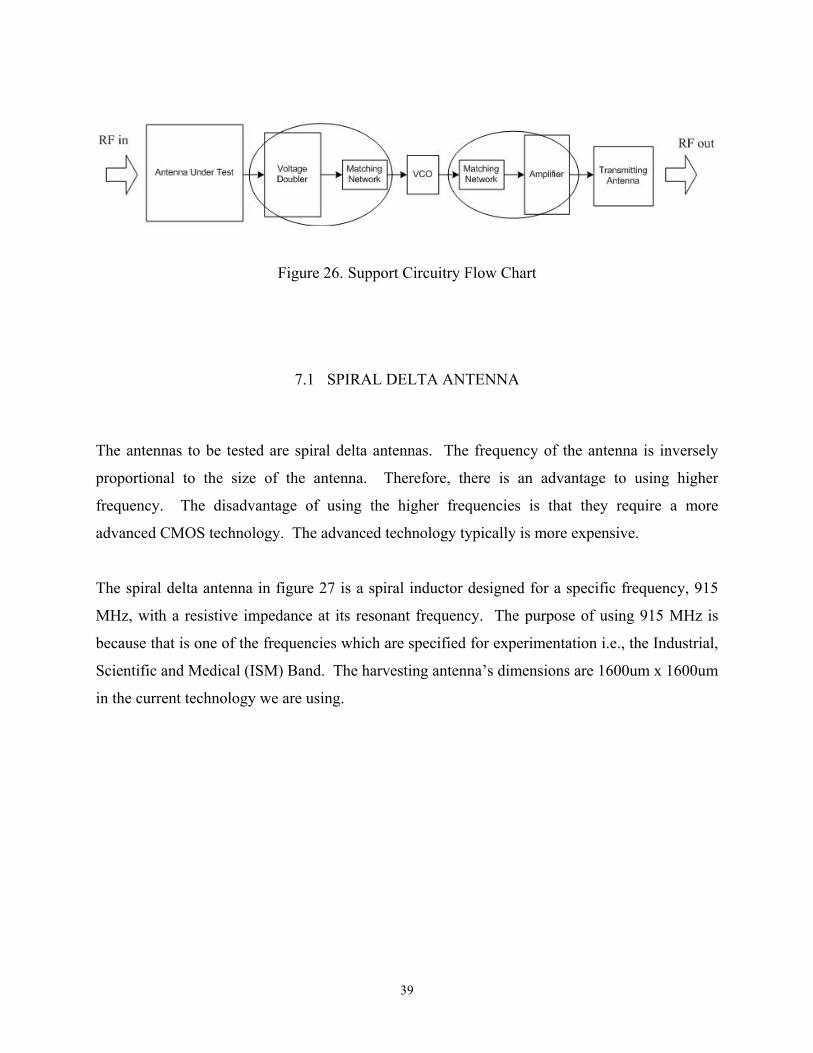
Figure 26. Support Circuitry Flow Chart
7.1 SPIRAL DELTA ANTENNA
The antennas to be tested are spiral delta antennas. The frequency of the antenna is inversely
proportional to the size of the antenna. Therefore, there is an advantage to using higher
frequency. The disadvantage of using the higher frequencies is that they require a more
advanced CMOS technology. The advanced technology typically is more expensive.
The spiral delta antenna in figure 27 is a spiral inductor designed for a specific frequency, 915
MHz, with a resistive impedance at its resonant frequency. The purpose of using 915 MHz is
because that is one of the frequencies which are specified for experimentation i.e., the Industrial,
Scientific and Medical (ISM) Band. The harvesting antenna’s dimensions are 1600um x 1600um
in the current technology we are using.
39

Figure 27. The Spiral Delta Antenna
7.2 CHARGE PUMP
The charge pump, or voltage doubler is a very important aspect in the design. It converts the AC
power into useable DC power. In general, power is a constant (in the ideal case), while voltage
is increased at the expense of current i.e., constant power. The efficiency of this component will
help determine the amount of source power needed to be directed at the chip, and consequently
the maximum distance at which the chip will be effective.
A voltage doubler can be implemented with two diodes and two capacitors as shown in figure
28. The layout of the voltage doubler is shown in figure 29.
40
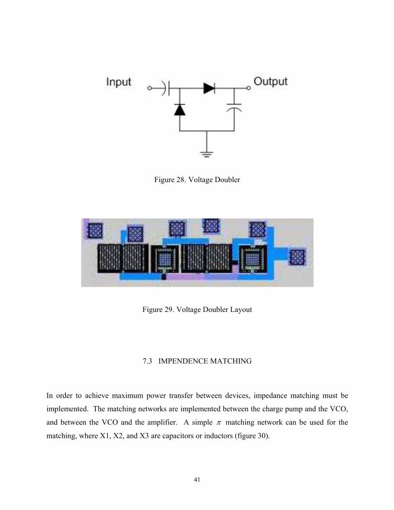
Figure 28. Voltage Doubler
Figure 29. Voltage Doubler Layout
7.3 IMPENDENCE MATCHING
In order to achieve maximum power transfer between devices, impedance matching must be
implemented. The matching networks are implemented between the charge pump and the VCO,
and between the VCO and the amplifier. A simple π matching network can be used for the
matching, where X1, X2, and X3 are capacitors or inductors (figure 30).
41

Figure 30. A Simple π Matching Network
An impedance network can be optimized for maximum voltage or for maximum current
exchange. A normal matching network is designed to transfer maximum power, of course,
resulting in a particular current and voltage. A technique of impedance miss-matching is
sometimes used to maximum the voltage of the transfer. This is important because the voltage
must be large enough to turn on and off transistors.
7.4 AMPLIFIER
The amplifier is necessary for transmitting the VCOs output frequency with sufficient power to
communicate with a receiver. The signal from the VCO is usually not strong enough to transmit
a reasonable distance without being amplified. The signal can easily be received in a shielded
room, but such a laboratory would not make a reasonable test environment for testing practical
antenna efficiencies.
The amplifier used to amplify the VCOs voltage is a typical low noise amplifier with a wide
tuning range to cover the range of VCO frequencies.
42

Figure 31. Low Noise Amplifier
43

8.0 AVAILABLE TEHCNOLOGIES
The technology that we used for our fabrication was very outdated and inexpensive. We make
use of the AMI ABN 1.5 process. The process consists of 2 polysilicon, 2 metal layers, 1.5
micron, 5 volts operation, n-well, CMOS, technology. The advantage of using the older
technology is the inexpensive fabrication price. A 0.5 micron fabrication would have cost us
five times as much per run. We primarily were concerned with fabricating analog circuits so the
limited metal layers, and high voltage was not as critical. The older technology did however
make some designs, and layouts challenging.
Designing a low powered VCO to fit the specific project requirements, discussed later, was
difficult with the AMI ABN 1.5. The necessity for multiple prototype runs prevented us from
choosing a more expensive technology. The antenna designs that were fabricated with the VCO
circuitry did not require an advanced technology to achieve the required results. With the
inexpensive technology, the antennas could be tested and redesigned for a fraction of the cost of
a more advanced technology.
We did consider moving to a more advanced technology. AMI’s C5N was the most favorable
among the considered processes. This 0.5 micron technology has 3 metal layers, 2 polysilicon
layers, 5 volts operation, n-well, CMOS technology. The C5N technology would have allowed
us to decrease the size of the chip. The 5 volts required for operation was the reason that
prevented us from moving to it. The size of the digital circuitry, needed for an ID TAG, would
be reduced, but the amount of power required to run it would not.
44

In order to simulate and test the circuit before sending it out for fabrication the detailed
technology files are required. Attaining the detailed technology files for some fabrication
processes was not possible. The confidential files had been available to educational groups.
MOSIS, a low-cost and small-volume prototyping service, changed their policy, and will not
release the required files to non-commercial groups [34].
Another reason for not moving to a more expensive technology was the lack of multiple
polysilicon layers. The majority of processes only have one polysilicon layer available. The
multiple polysilicon layers are important in the design of capacitors. The size of the capacitor
would greatly increase if the capacitance was formed with a metal layer. The reduction in size
due to the smaller feature size would be forfeited due to the size of the capacitors.
45
9.0 THE VCO DESIGN AND VERIFICATION EXPERIEMENTS
Two experiments were completed as steps to using a VCO to test energy harvesting antennas.
The first experiment was to design, simulate, fabricate and test a low powered VCO.
The second experiment was to transmit the VCOs frequency to a receiving antenna and measure
its results on a spectrum analyzer using a connected voltage source. These results were
compared with the results from the first experiment and are reported in this thesis.
9.1 OSCILATOR DESIGN
9.1.1 Experiment Description
9.1.1.1 Objective
The objective of this experiment was to design and fabricate a low powered voltage controlled
oscillator with a predictable linear frequency range. The function of the VCO is to test the
amount of power harvested by an antenna. The phase noise and Q (quality) factor of the circuit
were not as important as a constant Kvco. A constant Kvco would lead to a linear input voltage vs.
frequency curve. The advantage of a linear curve is the precision of mapping the input power
with the output frequency. A linear curve will allow more accurate conversions for received
frequencies between the measured points.
46
A wide frequency range is also important. A wide frequency range will decrease the amount of
error in calculating the input voltage. If the tuning range of a VCO is over 100 MHz then an
estimation of a specific frequency on the curve will be close, whereas if the tuning range is 10
MHz then the magnitude of the error can be much greater.
The design was also to be made as small as possible, i.e., minimum area of chip real-estate. The
amount of space that is available on future chips may be limited. The VCO is going to be used
to test the antennas and should not take up too much of the chip’s area. It has also been shown in
other research efforts that the circuitry in the area of an antenna will affect the performance of
the antenna. Large antenna designs may be necessary and the VCO should not prevent a large
antenna from fitting on the chip.
9.1.1.2 Background Information
Topology Selection
There are a number of different topologies that could be used as a template for the VCO. A
current-starved ring oscillator was chosen as the topology for the VCO design. The reason for
this selection was the current starved topology consumes less power then the other VCO
topologies. The majority of documented VCO topologies require more power than tolerable. It
also has the widest tuning range and is smallest in chip area used. The tuning range of the
current starved oscillator is nearly six times the size of the next best topology. The size of the
current starved oscillator is also a faction of the size of any other topology. The reason for its
small size is due to the lack of large components like capacitors, inductors and diodes. The
transistors used are extremely small compared to those used in other topologies. Its largest
transistor is typically smaller than the smallest transistor used in an LC VCO.
The lenient requirements for the quality of the signal also make the current starved oscillator the
topology of choice. The phase noise of the current-starved oscillator is poor compared to most
other topologies. The phase noise has very little bearing on our future use of the VCO so this
negative factor is not important.
47

Its other major flaw is the low Q values. The Q value is normally important in most applications.
The low Q is acceptable due to the large tuning range of the VCO. The frequency may be shifted
slightly in either direction due to the lack of quality of the circuit, but the little shift will be a
small percentage of change with respect to the tuning range. Therefore, accurate measurements
can still be achieved.
Overall the current starved oscillator fits the requirements the best. It is best suited in the areas
of importance and has weaknesses in areas that are not critical. It is also much easier to design
then most of the other topologies.
Oscillator Design
There were a multiple current starved oscillator topologies to choose from. The topology that
was chosen was the basic current starved oscillator in figure 12. The performance differences
between that oscillator, the simple oscillator (figure 13), and the full oscillator (figure 11) are
very subtle. The reason for this selection was the buffer on the output that strengthens the signal.
Sizing the components was the next task after choosing a topology. In order to conserve space
the smallest transistor sizes possible were used as shown in figure 32. The PMOS transistors in
the ring oscillator loop are the minimum size, 4.5µ m. The NMOS transistors were sized at
18µ m. The larger NMOS transistors are necessary to pull the signal back down to ground.
The current starved transistor, M3, is sized at 60µ m. It must be at least 3 times the size of the
NMOS transistors in the ring oscillator for it to draw enough current to greatly affect the
propagation delay in the ring. The output buffer is simply two inverters. The PMOS is also
minimum width and the NMOS is twice the size.
48

Figure 32. Current Starved Oscillator with Sizes
Simulations
Oscillators are difficult to simulate due to their physical inability to start without any external
input signals. Simulators have difficulty during the start of the oscillation due to needing to
initiate the circuit noise’s effect on the unstable circuit. Oscillators operate in an unstable state
and require a little bit of noise or jitter to get jumpstarted. Software normally doesn’t account for
such noises in a circuit, resulting in making it difficult to initiate oscillation.
There were two software packages available for this research that took into account the necessary
circuit noise required for oscillation. The two software packages were Ansoft’s Serenade, and
APLAC. The two software packages solve these problems differently.
APLAC requires the user to manually input the predicted noise. It accepts a current at a
specified frequency. The specified noise is then injected into the circuit at a point that must be
specified. Due to unpredictable process variations and complex calculations needed to predict
49
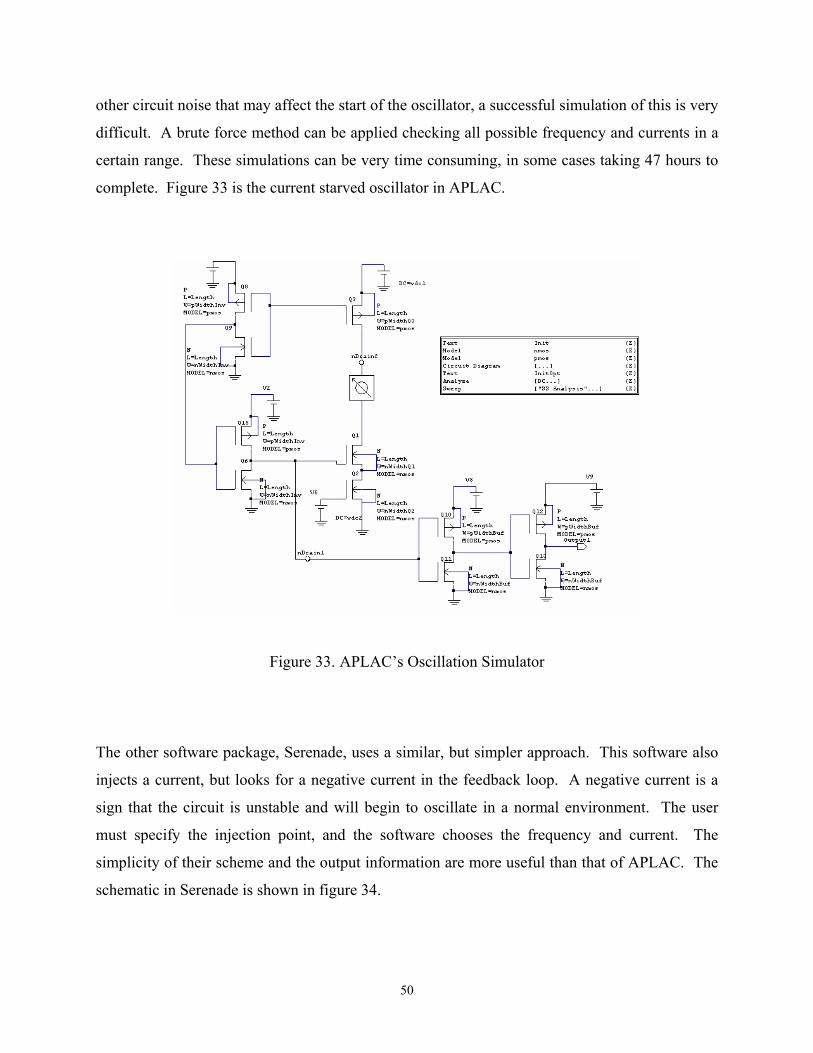
other circuit noise that may affect the start of the oscillator, a successful simulation of this is very
difficult. A brute force method can be applied checking all possible frequency and currents in a
certain range. These simulations can be very time consuming, in some cases taking 47 hours to
complete. Figure 33 is the current starved oscillator in APLAC.
Figure 33. APLAC’s Oscillation Simulator
The other software package, Serenade, uses a similar, but simpler approach. This software also
injects a current, but looks for a negative current in the feedback loop. A negative current is a
sign that the circuit is unstable and will begin to oscillate in a normal environment. The user
must specify the injection point, and the software chooses the frequency and current. The
simplicity of their scheme and the output information are more useful than that of APLAC. The
schematic in Serenade is shown in figure 34.
50

Figure 34. Ansoft’s Oscillator Simulator
9.1.1.3 Test Setup
Chip layouts
Four VCO designs that met the predetermined design requirements were successfully fabricated
and tested.
51

One single chip was used in this experiment to fabricate all four designs. The chip contained two
patch antennas on the top and the bottom and four VCOs spaced out through the middle. The
two patch antennas shown in figure 35 were used in a different experiment and are not a part of
the current VCO research.
Figure 35. VCO Chip with the Patch Antennas
The current-starved topology has many characteristics similar to a digital circuit. It uses
relatively small transistors, and it does not contain any inductors, resistors or capacitors. Those
characteristics make it difficult to use normal analog layout techniques. Normal analog layout
techniques would include mirroring, dummy elements, using unit sizes, separate guard rings, and
fingered transistors to name a few. Due to the lack of strictly analog qualities the same circuit
was designed in both an analog and a digital style layout.
52

A differential analog circuit will have two of each component. The mirroring layout technique
makes two identical layouts of the matching component and then positions them so the
component is symmetrical. An example of a symmetrical circuit can be view in figure 36.
Figure 36. Example of a Circuit Using a Mirroring Technique
Dummy elements are used to protect metal layers from inconsistent process itching. The dummy
elements are placed on the outside of the element that it is to protect. This prevents the inner
elements from receiving less itching than the outer elements during the fabrication process. A
block diagram using dummy elements is in figure 37.
53

Figure 37. Dummy elements outside of the protected elements
Unit sizes are important to keep the ratio of process etching effects consistent from component to
component of different sizes. Only the outer edge of a component is affected by etching. A unit
can be made with different dimensions resulting in a different amount of edge that is exposed to
etching effects. Using unit sizes will allow two elements of different sizes receive the same
percentage of etching effects. In figure 40 three different capacitors are using basic unit blocks
to form the specified size. The center capacitor is one unit block. The middle two on the top and
bottom are two unit blocks and the third is formed by the four unit blocks in the corner. Figure
38 is an example of using an unit to make larger components.
4C
2C C
Figure 38. An example of using unit sizes
54
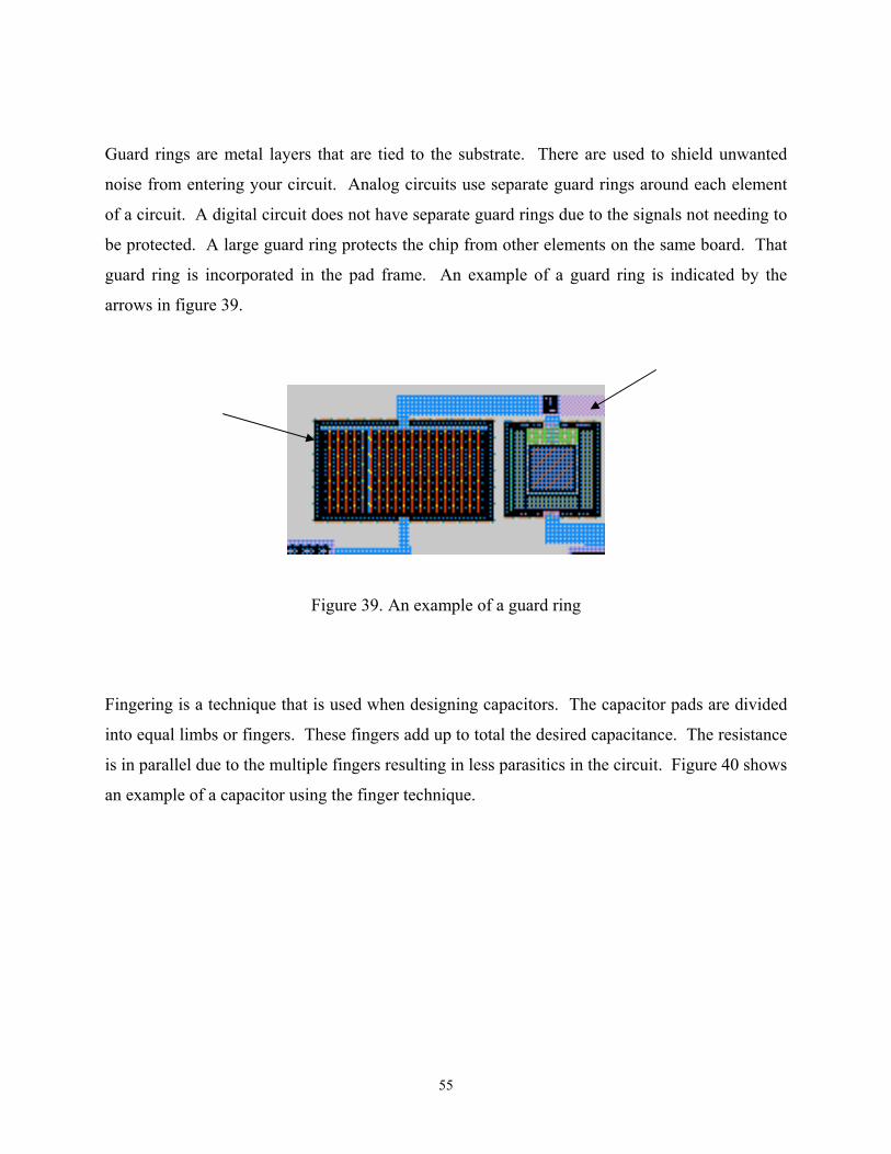
Guard rings are metal layers that are tied to the substrate. There are used to shield unwanted
noise from entering your circuit. Analog circuits use separate guard rings around each element
of a circuit. A digital circuit does not have separate guard rings due to the signals not needing to
be protected. A large guard ring protects the chip from other elements on the same board. That
guard ring is incorporated in the pad frame. An example of a guard ring is indicated by the
arrows in figure 39.
Figure 39. An example of a guard ring
Fingering is a technique that is used when designing capacitors. The capacitor pads are divided
into equal limbs or fingers. These fingers add up to total the desired capacitance. The resistance
is in parallel due to the multiple fingers resulting in less parasitics in the circuit. Figure 40 shows
an example of a capacitor using the finger technique.
55
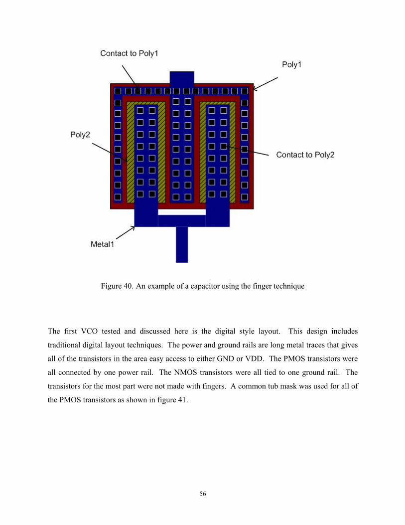
Figure 40. An example of a capacitor using the finger technique
The first VCO tested and discussed here is the digital style layout. This design includes
traditional digital layout techniques. The power and ground rails are long metal traces that gives
all of the transistors in the area easy access to either GND or VDD. The PMOS transistors were
all connected by one power rail. The NMOS transistors were all tied to one ground rail. The
transistors for the most part were not made with fingers. A common tub mask was used for all of
the PMOS transistors as shown in figure 41.
56

Figure 41. Digital Style VCO layout (VCO1)
The second VCO was an analog style layout. The transistors do not share a common rail for
ground or power. The transistors were designed with fingers. Each PMOS transistor has its own
tub mask layer. There is a ground ring which encloses the entire circuit as shown in figure 42.
57

Figure 42. Analog Style VCO layout (VCO2)
The first two VCOs had the VDD and Vcont inputs wired to the same pad. The third and fourth
VCOs were made exactly like the first and second respectively, but the VDD and Vcont inputs
were wired to different pads instead of sharing one common rail. The reason for that is so the
noise from one power source does not affect transistors attached to the other power source.
The advantage of connecting the VDD and Vcont inputs is only one power source is required.
Only needing one power supply allows the VCO to be directly connected to the antenna in future
experiments. The frequency range is also much wider when they are connected. A disadvantage
of connecting the two inputs is the output power is lower when lower voltages are applied to the
input. This may affect future testing of antennas that may harvest low voltages. The faint output
signal may be difficult to detect.
58

Test rig
The VCO was put on a test rig so input and output cables can be attached to them. The test rig
was made with FR4 printed circuit board (PCB) with copper traces. The test rig has five copper
posts and four SMA connectors soldered to it. The posts are necessary to wire-bonding to them.
The input/output of the SMA connectors were connected to each of the copper posts. The other
copper post was grounded. The VCO test rig can be seen in figure 43.
Figure 43. The VCO Test Rig
Wire bonds
To attach the SMA connector the chip containing the VCO wire bonds are necessary. The
bonding wire is made of aluminum. Its thickness is 25.4µm. There are three bonds. The first
bond is connected from the ground pin of the test rig to the ground pad of the VCO. The second
bond is connected to the pin, which is connected to the SMA input. The third bond was
connected from the output pad of the VCO to the input pad of the spectrum analyzer. The three
wire bonds can be viewed in figure 44.
59
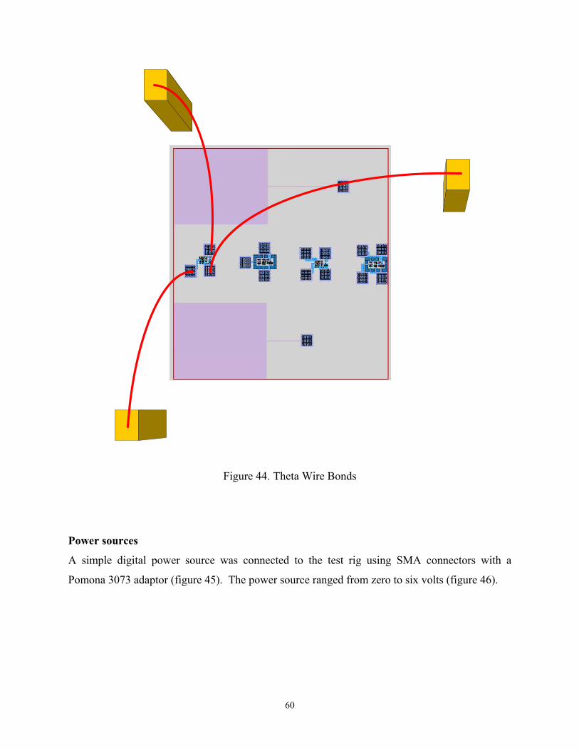
Figure 44. Theta Wire Bonds
Power sources
A simple digital power source was connected to the test rig using SMA connectors with a
Pomona 3073 adaptor (figure 45). The power source ranged from zero to six volts (figure 46).
60

Figure 45. Pomona 3073 Power Adaptor
Figure 46. Power Supply
Network analyzer
An E4403B Agilent spectrum analyzer was used to detect the output frequency. The analyzer
was set at a frequency range of 100 MHz to 600 MHz. The range of the test window was 500
MHz. The results can be easily seen in a RF shielded room. The results in an uncontrolled
environment had to be averaged to easily observe transmission results.
61

Equipment Setup
The test required one power supply, a spectrum analyzer, wires for connections and the test rig as
mentioned before. The DC power supply was directly connected to the test rig with coaxial
cables. The output of the VCO was directly connected to the spectrum analyzer. A diagram of
the setup can be seen in figure 47.
Figure 47. VCO Test Setup
9.1.2 Results
The experiment was a success. All four of the VCOs that were fabricated preformed better than
the simulations indicated. The tuning frequency range was about 4 times as wide as the
62

simulations. The amount of power consumed by the actual VCO (3mW) was also less than the
power consumed in simulation (12mW). Kvco of the actual layout was closer to constant than
expected.
The excellent results are hard to explain for certain. Both simulators use estimations and
approximations to determine the output. There is a degree of error in both programs. That may
account for some of the difference in the results. The models of the MOS transistors may not
have been exactly the same as what was fabricated. The models used were results from previous
fabrication runs. There are three chip runs between the results used for simulation and the
fabrication. There may have been changes made. The output signal was much weaker than that
of the simulation. That explains why less power was consumed. The 1.5 AMI process has a
transistor speed limitation. The frequency is in the range, but some gain is lost at that frequency.
Both programs have been known to bad results before. Using their software it is possible to
successfully simulate frequencies which are well above the technology’s limitations.
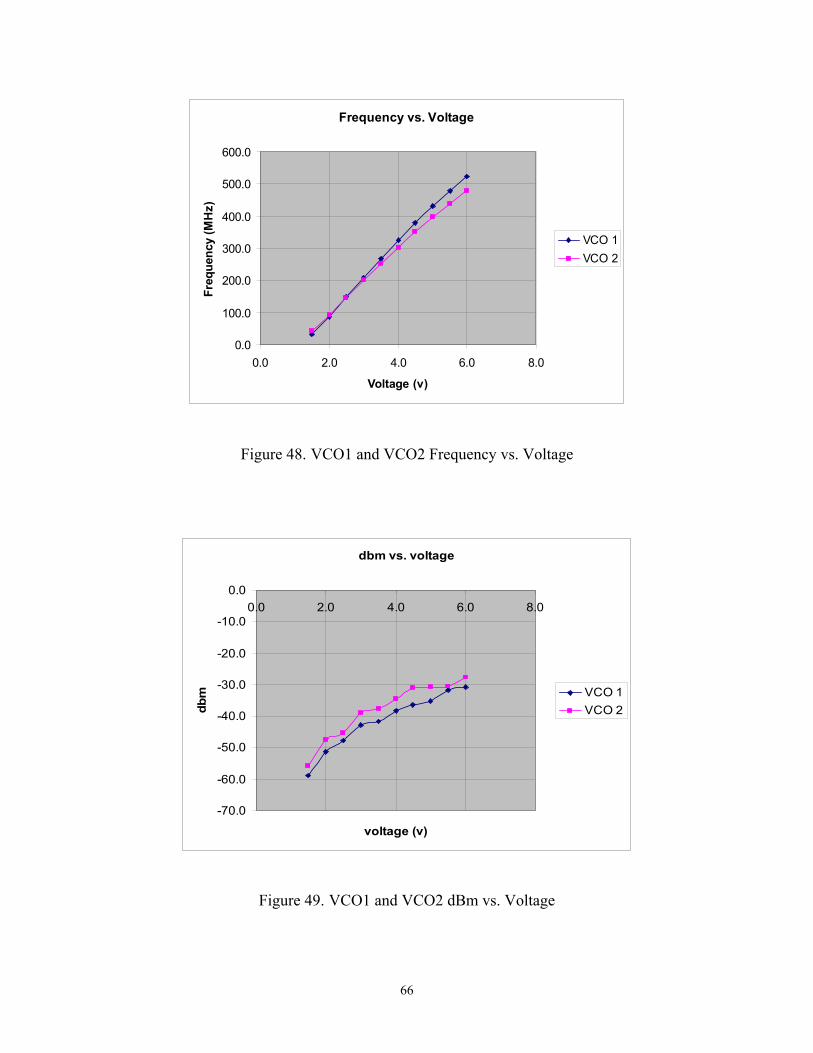
9.1.2.1 VCO 1 Results
The first VCO was the digital style layout. The average Kvco was 109.06 rads/s/V. The standard
deviation was 11.73 rads/s/V. The signal to noise ratio ranged from 2.9 dBm at 1.5v to 30.4
dBm at 6v. Table 2 displays the measured results from VCO1.
63

Table 2. VCO1 (digital) Analyzer Results
VCO1 (digital)
Voltage Frequency dbm1.5 33.0 -58.92.0 86.8 -51.22.5 147.7 -47.83.0 209.1 -42.73.5 268.9 -41.74.0 326.0 -38.34.5 380.2 -36.55.0 431.2 -35.35.5 478.9 -31.76.0 523.8 -30.7
noise level: -61.4 dbmfrequency swing: 490.75 MHz
The second VCO, the analog style layout, performed equally as well. The frequency range was
less than that of VCO1 by 53.05 MHz. The average KVCO was 97.04 rads/s/V. Its standard
deviation was 10.34rads/s/V which was better than the digital VCO. The noise level, -61.94
dBm, was lower than the first VCO. The measured results from VCO2 can be viewed in table 3.
64

Table 3. VCO2 (analog) Analyzer Results
VCO2 (analog)
Voltage Frequency dbm1.5 41.7 -55.92.0 91.7 -47.52.5 146.0 -45.53.0 200.4 -39.13.5 253.0 -37.54.0 303.1 -34.44.5 351.2 -31.05.0 395.6 -30.85.5 438.7 -30.56.0 478.4 -27.6
noise level: -61.9 dbmfrequency swing: 436.70 MHz
The results of the two the frequency versus voltage are plotted on a graph in figure 48. The two
VCOs signal strengths are compared in figure 49.
65
Frequency vs. Voltage
0.0
100.0
200.0
300.0
400.0
500.0
600.0
0.0 2.0 4.0 6.0 8.0
Voltage (v)
Freq
uenc
y (M
Hz)
VCO 1VCO 2
Figure 48. VCO1 and VCO2 Frequency vs. Voltage
dbm vs. voltage
-70.0
-60.0
-50.0
-40.0
-30.0
-20.0
-10.0
0.00.0 2.0 4.0 6.0 8.0
voltage (v)
dbm VCO 1
VCO 2
Figure 49. VCO1 and VCO2 dBm vs. Voltage
66

9.2 TRANSMISSION I EXPERIMENT
The purpose of the transmission experiment was prove the antennas could transmit a VCOs
signal and be received. The reason for this step is to prove the antennas transmitting capabilities.
The experiment was implemented by simulating the harvesting antenna with a DC power supply
and then transmitting the results via transmitting antenna to a nearby receiving antenna which
was connected to a network analyzer.
9.2.1 Description
9.2.1.1 Objective
The objective of the experiment was to accurately measure the amount of power being
transmitted without touching the chip with test equipment from a connected power source. The
results were then compared to the results from the previous experiment. This is in tended to
prove the antenna’s transmitting ability and show consistent voltage verse frequency of the VCO
from test to test.
The test will determine if using an amplifier to boost the signal from the VCO could be avoided.
The power consumed by the amplifier could make testing the envelope of the antenna’s
performance difficult. Another reason was to determine what the lowest voltage that could be
converted, transmitted, and received in a normal test environment.
The possibility of the faint signal from a non-amplified VCO may not be distinguishable in a
normal RF environment. This concern also prompted this test. If the signal to noise ratio is high
enough then future tests will not need to be conducted in an RF shielded room. The advantage of
67
not using an RF shielded environment enables us to test the antennas in some of the actual
environments that they might be used.
9.2.1.2 What was accomplished
The experiment successfully transmitted an RF signal from a voltage controlled oscillator, which
was used to determine the energy supplied by the power source. It proves the transmitting ability
of the delta spiral antenna. This also makes it possible to test the amount of power received from
an energy harvesting antenna without connecting test equipment to it. The VCO and
transmitting antenna have successfully transmitted the power, therefore when powered by the
harvesting antenna and then converted to DC via the voltage doubler the amount of energy
harvested can be determined.
The test was conducted in both an RF shielded room and in two different open environments.
The first test, in the shielded, room was done to prove that the concept worked. The signal is
easier to find on a Spectrum Analyzer due to the interfering noise that is shielded by the room.
The second test was conducted in the laboratory in 570 Benedum Hall. The laboratory test
proved that the concept would work in most environments. Other RF devices and testing
equipment are also in the room. The signal was strong enough to be distinguished over the
ambient noise in the room. Finding the signal was more challenging in that environment, but
possible since the outputted frequency is known. If the frequency is not known it can still be
found, but may require more time.
The third test was setup in a hotel lobby during as normal business day. The test was setup as a
demonstration to show the ability to transmit in a normal everyday environment. It was also a
successful. No measurements were taken from this test as the test was demonstrated for various
Pittsburgh Digital Greenhouse members.
68

9.2.1.3 Test Rig Setup
Chip layouts
Two chips were used in this experiment. The first chip, Theta (figure 50), contained two patch
antennas, one on the top and one on the bottom and four VCOs spaced throughout the middle.
The second chip, Epsilon (figure 51, contains four spiral (delta) antennas, four voltage doublers,
and two dipole antennas.
Figure 50. Theta chip
69
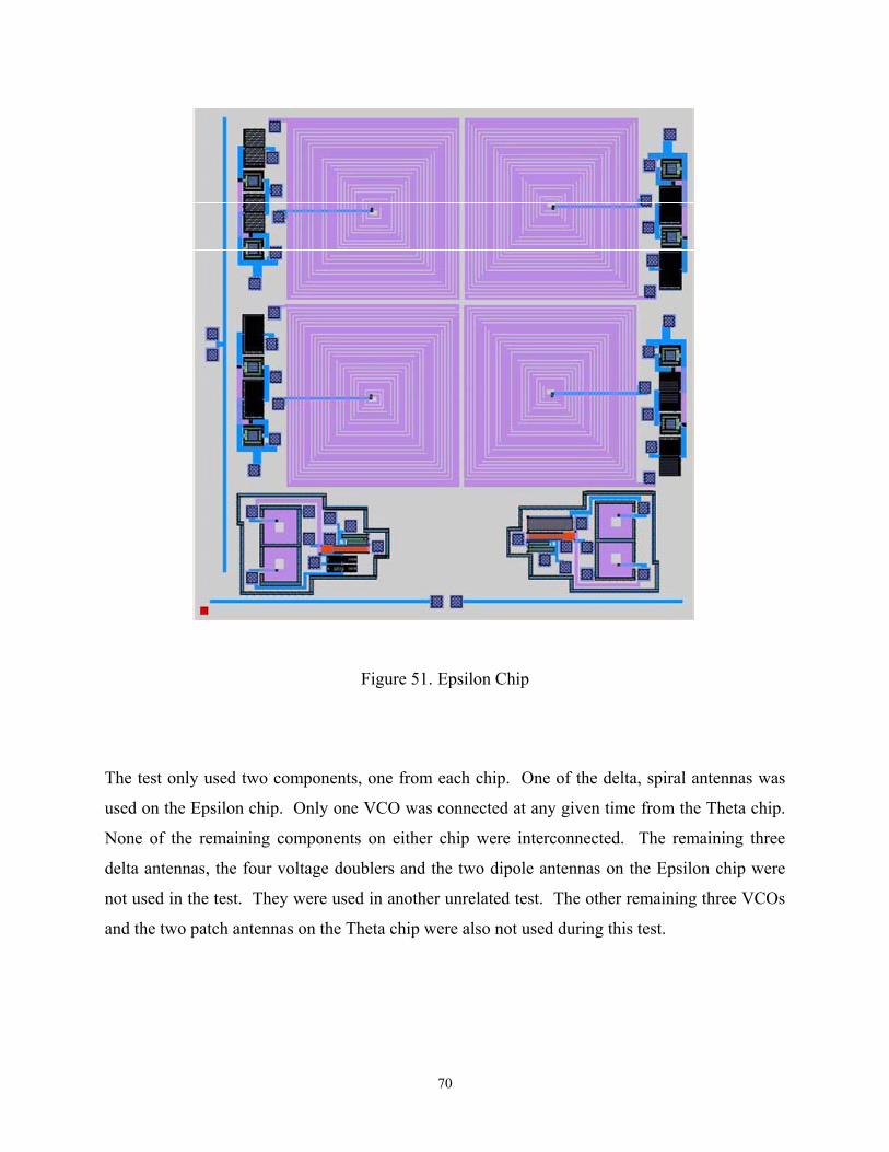
Figure 51. Epsilon Chip
The test only used two components, one from each chip. One of the delta, spiral antennas was
used on the Epsilon chip. Only one VCO was connected at any given time from the Theta chip.
None of the remaining components on either chip were interconnected. The remaining three
delta antennas, the four voltage doublers and the two dipole antennas on the Epsilon chip were
not used in the test. They were used in another unrelated test. The other remaining three VCOs
and the two patch antennas on the Theta chip were also not used during this test.
70

Test rig
The test rig is made of FR4 PCB with copper traces. The test rig has two copper posts which
were used as pins and one SMA connector soldered to it. The input of the SMA connector was
connected to one of the copper post. The other copper post was grounded. A top view of the test
rig is shown in figure 52.
Figure 52. Test Rig
Wire bonds
The bonding wire for this experiment was aluminum wire with a thickness of 25.4µm. There
were three bonds. The first bond was connected from the ground pin of the test rig to the ground
pad of the VCO. The second bond was connected from the VDD, SMA input to the input pad of
the VCO. The third bond was connected from the output pad of the VCO to the input pad of the
antenna. The bonds can be seen in figure 53.
71

Figure 53. Bonding Diagram of Transmission Experiment
9.2.1.4 Equipment Setup
Power source
A simple DC power source was connected to the test rig using SMA connectors with a Pomona
3073 power adaptor (Figure 45). The power source ranged from zero to six volts. The power
source sitting to the left of the network analyzer can be seen in figure 54.
72
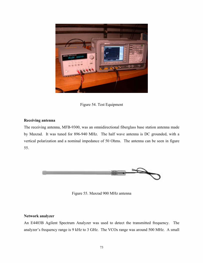
Figure 54. Test Equipment
Receiving antenna
The receiving antenna, MFB-9300, was an omnidirectional fiberglass base station antenna made
by Maxrad. It was tuned for 896-940 MHz. The half wave antenna is DC grounded, with a
vertical polarization and a nominal impedance of 50 Ohms. The antenna can be seen in figure
55.
Figure 55. Maxrad 900 MHz antenna
Network analyzer
An E4403B Agilent Spectrum Analyzer was used to detect the transmitted frequency. The
analyzer’s frequency range is 9 kHz to 3 GHz. The VCOs range was around 500 MHz. A small
73
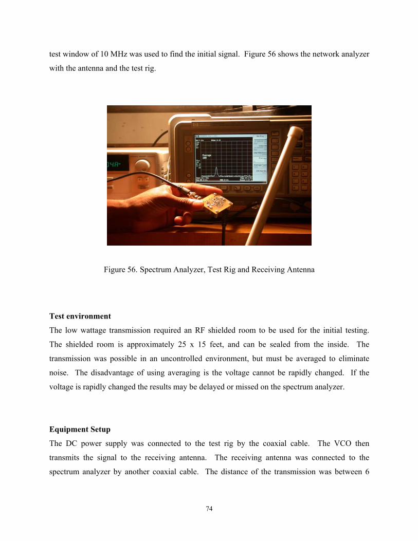
test window of 10 MHz was used to find the initial signal. Figure 56 shows the network analyzer
with the antenna and the test rig.
Figure 56. Spectrum Analyzer, Test Rig and Receiving Antenna
Test environment
The low wattage transmission required an RF shielded room to be used for the initial testing.
The shielded room is approximately 25 x 15 feet, and can be sealed from the inside. The
transmission was possible in an uncontrolled environment, but must be averaged to eliminate
noise. The disadvantage of using averaging is the voltage cannot be rapidly changed. If the
voltage is rapidly changed the results may be delayed or missed on the spectrum analyzer.
Equipment Setup
The DC power supply was connected to the test rig by the coaxial cable. The VCO then
transmits the signal to the receiving antenna. The receiving antenna was connected to the
spectrum analyzer by another coaxial cable. The distance of the transmission was between 6
74
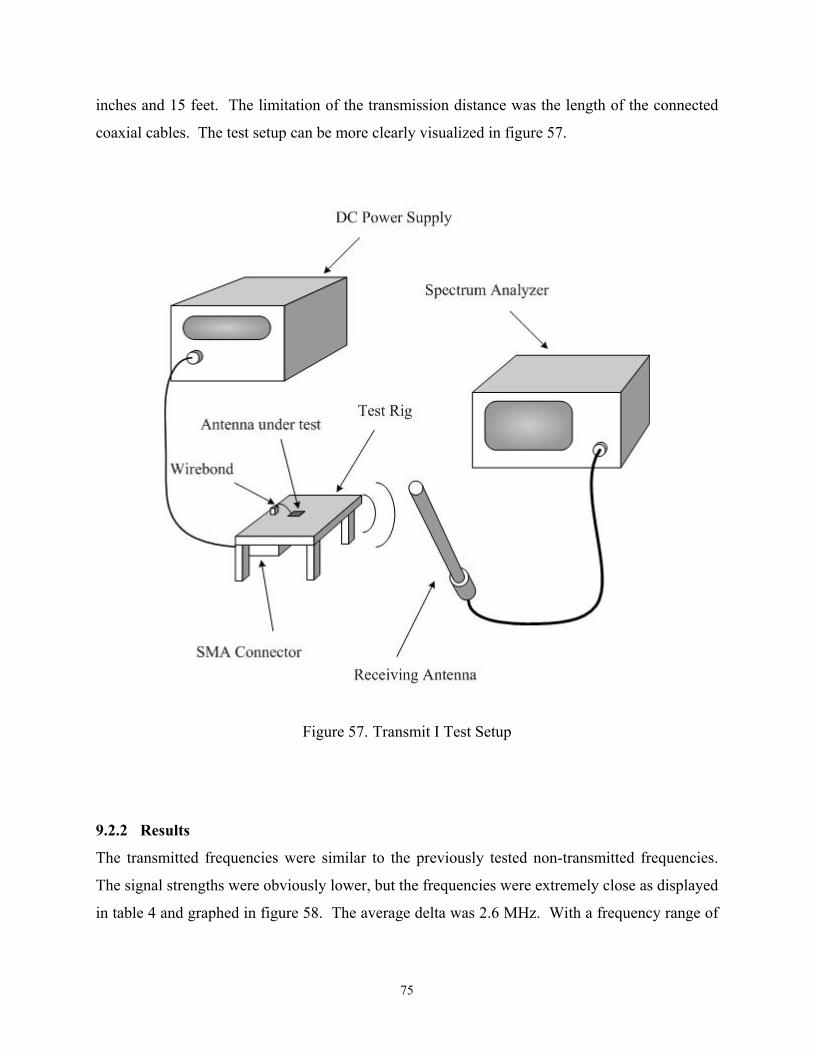
inches and 15 feet. The limitation of the transmission distance was the length of the connected
coaxial cables. The test setup can be more clearly visualized in figure 57.
Figure 57. Transmit I Test Setup
9.2.2 Results
The transmitted frequencies were similar to the previously tested non-transmitted frequencies.
The signal strengths were obviously lower, but the frequencies were extremely close as displayed
in table 4 and graphed in figure 58. The average delta was 2.6 MHz. With a frequency range of
75

over 400 MHz the average delta is negligible, making this experiment a success. The actual
signal can be seen on screen shots from the spectrum analyzer in figures 72-75.
Table 4. Transmitted Results Compared to the Non-Transmitted Results
Voltage Non-Trans Freq. Trans Freq. Delta3.0 209.1 208 1.13.5 268.9 267 1.94.0 326.0 323 3.04.5 380.2 377 3.25.0 431.2 428 3.25.5 478.9 476 2.96.0 523.8 521 2.8
Transmitted vs. Non-Transmitted
200
250
300
350
400
450
500
550
2.5 3.5 4.5 5.5 6.5
Voltage (V)
Freq
uenc
y (M
Hz)
TransmittedNon-Transmitted
Figure 58. Transmitted I Compared to Non-Transmitted Results
76

9.3 TRANSMISSION II EXPERIMENT
The purpose of the second transmission experiment was to transmit the VCOs frequency by
powering the VCO from harvested RF energy, which was converted to DC energy by the voltage
doubler. This is intended to prove both the antennas’ harvesting and transmitting ability. This
would also prove that a VCO used as a transducer can be used as a method of testing on-chip
antennas.
9.3.1 Description
9.3.1.1 Objective
The objective of the experiment was to accurately measure the amount of power being
transmitted without touching the chip. The results would then be compared to the results from
the previous two experiments. This would prove the antenna’s transmitting and harvesting
abilities and confirm consistent voltage verse frequency of the VCO from test to test.
9.3.1.2 What was accomplished
The experiment was unsuccessful. A single chip was fabricated and made that contained an
energy harvesting antenna, which is connected to a voltage doubler, which powers a VCO, who’s
signal is transmitted by a spiral, delta antenna. The name of the chip was Iota (figure 59). There
were two major factors contributing in Iota not functioning correctly. Both were based off of
limitations with the fabrication. Due to limited area available on the chip the largest two
antennas that would fit on the chip were tuned to 915 MHz and 2.45 GHz. The 915 MHz was
used for the energy harvesting, and the 2.45 GHz was used for transmitting. The RF energy was
focused at the chip at 915 MHz, but the transmitting frequency of the VCO was in the 100-600
MHz range. The 2.45 GHz antenna was not a good antenna for this situation.
77
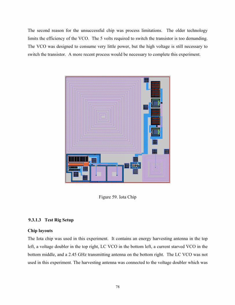
The second reason for the unsuccessful chip was process limitations. The older technology
limits the efficiency of the VCO. The 5 volts required to switch the transistor is too demanding.
The VCO was designed to consume very little power, but the high voltage is still necessary to
switch the transistor. A more recent process would be necessary to complete this experiment.
Figure 59. Iota Chip
9.3.1.3 Test Rig Setup
Chip layouts
The Iota chip was used in this experiment. It contains an energy harvesting antenna in the top
left, a voltage doubler in the top right, LC VCO in the bottom left, a current starved VCO in the
bottom middle, and a 2.45 GHz transmitting antenna on the bottom right. The LC VCO was not
used in this experiment. The harvesting antenna was connected to the voltage doubler which was
78

connected to the VCO. The VCO and the transmitting antenna were not connected. They were
left unconnected so it could be used in other experiments also.
Test rig
The test rig was also made of FR4 PCB with copper traces. The chip was attached to the test rig
using conductive epoxy. The purpose of attaching the chip was to prevent loosing the chip, and
to attach the chips ground/substrate to something.
Wire bonds
There was only one wire bond that was necessary, which was from the output of the VCO to the
input of the transmitting antenna. No wire bonds to the test rig were necessary. Figure 60 shows
the bond on the Iota chip.
Figure 60. Bonding Diagram of Transmission II Experiment
79

Equipment Setup
The test required that an RF source is used. To create the RF source to power the chip a signal
generator transmitting a sinusoidal wave was connected an RF amplifier. The amplifier boosts
the generator’s 20mW signal 10W. That is then transmitted by a Maxrad 900 antenna toward the
Iota chip. The Iota chip then transmitters the signal to another Maxrad 900 antenna, which is
connected to the spectrum analyzer. The test setup can be more clearly visualized in figure 61.
Figure 61. Transmitting II Test Setup
80

10.0 CONCLUSION
The conclusion of the experimental findings is that using VCOs to test the efficiency of an
antenna is possible. The method provides an accurate means of testing energy harvesting
antennas. This method does however require you to the VCO on the chip with the antennas
under test. This may be expensive, especially because cheaper processes cannot be uses as
explained earlier. The VCO can be bonded to the antennas, but this could affect the efficiency of
the antenna.
A problem that could be encountered using this method would be that the CMOS process
variation can change a VCOs performance. The change of performance cannot be measured
independently from the antenna to which it is connected. The results could contain some slight
errors. The margin of error would not be too great due to the possible change verse the very
large tuning range. If the VCO is designed with a small tuning range this could greatly affect
your results
Future research efforts could go into analyzing the thermal behaviors of the VCOs. The results
from all VCOs will change slightly as the temperature of the chip increases. If the thermal
qualities of the VCO are studied more closely they could be predicted and a more accurate
analysis of the antenna under test could be achieved.
81

11.0 CONTRBUTIONS
This research has contributed the following items to the way of science and engineering of a
VCO.
1. Identified and categorized the VCOs into three different types, LC, non LC, and special
components for use as an embedded wireless diagnostic measurement and communications
system.
2. Compiled the necessary characteristics of a VCO to be used as identified earlier in energy
harvesting applications. The compiled items are as follows: definition, multiple topologies,
uses, and currently researched efforts of a VCO.
3. Identify and document an appropriate basis topology and achieved better results. The
current starved topology shown in figure 12 was chosen for the experiments. In order to reduce
the amount of power consumed the buffer on the output was changed to two inverters. This
change reduced not only power, but also reduced the circuit size.
4. Demonstrated the advantage of tying the supply voltage and the control voltage together.
This greatly increased the tuning range and made it possible to use only one voltage source.
5. Designed, laid-out, and fabricated two VCOs with different styles (analog and digital) for
the sake of comparison. The two styles yielded different results, which are summarized and
reported.
6. Developed setup and executed a method of testing the two different VCOs using the data
from the tests as a reference for future tests.
82

7. Developed, setup, and executed a method of testing the transmitting antenna. The test
results were then compared to the previously documented results.
8. Developed an additional method to test an energy harvesting antenna.
83

APPENDIX A
VCO Comparison Test
11.1 VCO 1 Results
Figure 62. VCO 1 Analyzer Results: 1.5 Volts and 2.0 Volts
84

Figure 63. VCO 1 Analyzer Results: 2.5 Volts and 3 Volts
Figure 64. VCO 1 Analyzer Results: 3.5 Volts and 4 Volts
85

Figure 65. VCO 1 Analyzer Results: 4.5 Volts and 5 Volts
Figure 66. VCO 1 Analyzer Results: 5.5 Volts and 6 Volts
86

11.2 VCO 2 Results
Figure 67. VCO 2 Analyzer Results: 1.5 Volts and 2 Volts
Figure 68. VCO 2 Analyzer Results: 2.5 Volts and 3 Volts
87

Figure 69. VCO 2 Analyzer Results: 3.5 Volts and 4 Volts
Figure 70. VCO 2 Analyzer Results: 4.5 Volts and 5 Volts
88

Figure 71. VCO 2 Analyzer Results: 5.5 Volts and 6 Volts
89

APENDIX B
Transmission Experiment
11.3 Transmission Results
Figure 72. Transmitted Analyzer Results: 2.5 Volts and 3 Volts
90

Figure 73. Transmitted Analyzer Results: 3.5 Volts and 4 Volts
Figure 74. Transmitted Analyzer Results: 4.5 Volts and 5 Volts
91

Figure 75. Transmitted Analyzer Results: 5.5 Volts and 6 Volts
92
BIBLIOGRAPHY
1. Herzel, F.; Pierschel, M.; Weger, P.; Tiebout, M. “Phase Noise in a Differential CMOS Voltage-Controlled Oscillator for RF Applications.” IEEE Transactions on Circuits and Systems - II, Volume: 47 Issue 1 January 2000: 11 –15. 2. Kato, K.; Sase, T.; Hideo, S.; Ikushima, I.; Kojima S. “A Low-Power 128-MHz VCO for Monolithic PLL IC’s.” IEEE Journal of Solid-State Circuits, Volume 23, Number 2 April 1988: 474-479. 3. Razavi, Behzad. Design of Analog CMOS Intergraded Circuits. New York: McGraw-Hill, 2001. 4. Lee, Thomas. The Design of CMOS Radio-Frequency Integrated Circuits. New York: Cambridge University Press, 1998. 5. Dec, A.; Suyama K. “A 1.9-GHz CMOS VCO with Micromachined Electromechanically Tunable Capacitors.” IEEE Journal of Solid-State Circuits, Volume 35, Number 8 August 2000: 1231-1237. 6. Craninckx, J.; M. Steyaert, and H. Miyakawa. “A Fully Integrated Spiral-LC CMOS VCO Set with Prescaler for GSM and DCS-1800 Systems.” IEEE 1997 Custom Integrated Circuits Conference 1997: 736-744. 7. Svelto, F., S. Deantoni, R. Castello. “A 1.3 GHz Low-Phase Noise Fully Tunable CMOS LC VCO.” IEEE Journal on Solid State Circuits, Volume 35, Number 3 March 2000. 8. Andreani, P., S. Mattisson. “On the Use of MOS Varactor in RF VCO’s.” IEEE Journal of Solid-State Circuits, Volume 35, Number 6 June 2000. 9. Thamsirianunt, M, A. Kwasniewski. “CMOS VCO for PLL Frequency Synthesis in GHz Digital Mobile Radio Communications.” IEEE Journal of Solid-State Circuits, Volume 32, Number 10 October 1997. 10. Gottlieb, Irving. Practical Oscillator Handbook. Oxford: Newnes, 1997
93

11. Gray, Paul, P. J. Hurst, S. H. Lewis, and R.G. Meyer. Analysis and Design of Analog Integrated Circuits. John Willy & Sons, Inc. 2001. 12. Baker, R. J., H. W. Li, and D. E. Boyce. CMOS Circuit Design, Layout, and Simulation. IEEE Press. 1998. 13. Apparatus for Energizing a Remote Station and Related Method, U.S. Patent No. 6,289,237, University of Pittsburgh. Mickle, Marlin H., K. W. Wells, R. G. Hoelzeman. September 11, 2001 (40 claims). 14. Apparatus for Energizing a Remote Station and Related Method, Continuation In Part, Serial No. 09/951,032. University of Pittsburgh. Mickle, Marlin H., L. Mats, L. Neureuter, M. Mi, D. Gorodetsky, C. Taylor and C. Emahiser. Filed September 10, 2001 (55 claims). 15. http://www.radiolab.com.au 16. http://www.saronix.com 17. Ahrens, T. I., and T. H. Lee. “A 1.4-GHz 3-mW CMOS LC low phase noise VCO using tapped bond wire inductances.” Low Power Electronics and Design, 1998, 1998: pages 16-19. 18. Soga, Shuji, Y. Hiroshige, A. Dobashi, M. Okumura, and T. Kusuzaki. “Products Lifecycle Management System Using Radio Frequency Identification Technology.” 19. http://www.speedpass.com 20. http://www.ezpass.com 21. Razavi, Behzad. “A Study of Phase Noise in CMOS Oscillators.” IEEE Journal of Solid-State Circuits, Vol. 31, No. 3, March 1996: pages 331-343. 22. Herzel, Frank, H. Erzgraber and P. Weger. “Integrated CMOS Wideband Oscillator for RF Applications.” IEEE Electronics Letters, Vol. 37, Issue: 6, 15 March 2001: pages 330-331. 23. Herzel, Frank, H. Erzgraber and N. Ilkov. “A New Approach to Fully Integrated CMOS LC-Oscillators with a Very Large Tuning Range” Custom Integrated Circuits Conference, 2000. CICC Proceedings of the IEEE 2000, 2000: pages 573-576. 24. Hung, Chih-Ming, L. Shi, I. Languado, and K. K. O. “A 25.9-GHz Voltage Controlled Oscillator Fabricated in a CMOS process.” VLSI Circuits, 2000. Digest of Technical Papers. 2000 Symposium on, 2000: pages 100-101. 25. Wilson, William, Un-Ku Moon, K. Lakshmikumar, L. Dai. “A CMOS Self-Calibrating Frequency Synthesizer.” IEEE Journal of Solid-State Circuits, Vol. 35, No. 10, October 2000: pages 1437-1444.
94
95
26. Hung, Chih-Ming, B. Floyd, N. Park, and K. K. O. “Fully Integrated 5.35-GHz CMOS VCOs and Prescalers.” IEEE Transactions on Microwave Theory and Techniques, Vol. 49, No. 1, January 2002: pages 17-22. 27. Andreani, Pietro. “A 1.8-GHz Monolithic CMOS VCO Tuned by an Inductive Varactor.” Circuits and Systems, 2001. ISCAS 2001. The 2001 IEEE International Symposium on, Vol. 4, 2001: pages 714-717. 28. Andreani, Pietro and S. Mattisson. “A 2.4-GHz CMOS Monolithic VCO Based on an MOS Varactor.” 29. Andreani, Pietro. “A 1.8-GHz CMOS VCO Tuned by an Accumulation-Mode Varactor.” Circuits and Systems, 2001. ISCAS 2001. The 2001 IEEE International Symposium on, Vol. 4, 2001: pages 714-717. 30. Pott, V., and others. “The Suspended-Gate MOSFET (SG-MOSFET): A Modeling Outlook for the Design of RF MEMS Switches and Tunable Capacitors.” 31. Dec, A.; Suyama K. “RF Micromachined Varactors with Wide Tuning Range.” Radio Frequency Integrated Circuits Symposium, 1998 IEEE. 7-9 Jun 1998: pages 309-312. 32. De Ranter, C. R. C., M. S. J. Steyaert. “A 0.25 um CMOS 17 GHz VCO.” Solid-State Circuits Conference, 2001. Digest of Technical Papers. ISSCC. 2001 IEEE International. 2001: pages 370-371, 466. 34. http://www.mosis.org