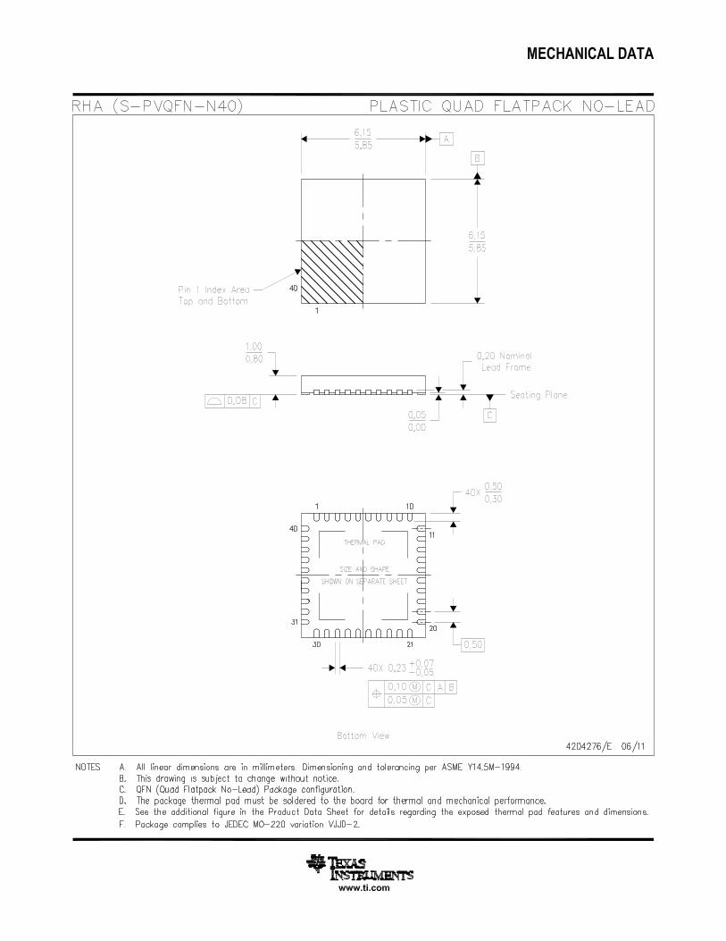
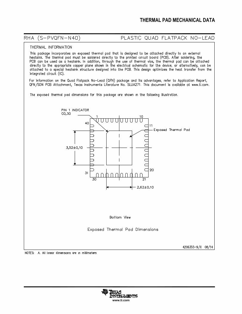
tps65251 4.5-v to 18-v input, high-current, … type package drawing pins package qty eco plan (2)...
TRANSCRIPT
TPS
65251
C25
R22 C24
R20
R21L2
GND
VIN
LX3
VIN
L 3X
GND
C23
BST3VIN3
EN3
L 2X
BST2
L 1X
VIN2
L 2X
EN2
VIN1
EN1
LX1
BST1
C11
R10
R11
L1
C13R13
C15
R12 C14
V2
V1
VIN1C10
C27
4.7 nF
C17
VIN
C35
R32C34C36
R1
C26
C21
F 2B
F 2B
PG
C 1
C2
C37
C31
R30
R31
C33
V3
C30
VIN3
VIN
C20VIN2
C16
L3
4.7 µH
R23
R33120 k
GPIO or GND
GPIO or GND
CM
P2
GN
D
F2
B
LOW
_P
S2
S
V7V
AG
ND
PG
OO
D
V3V
RLI
M2
FB
1
SS
1
SY
NC
CM
P1
RO
SC
RLI
M1
CM
P3
RLI
M3
FB
3
S3
S
Copyright © 2018, Texas Instruments Incorporated
Product
Folder
Order
Now
Technical
Documents
Tools &
Software
Support &Community
ReferenceDesign
An IMPORTANT NOTICE at the end of this data sheet addresses availability, warranty, changes, use in safety-critical applications,intellectual property matters and other important disclaimers. PRODUCTION DATA.
TPS65251SLVSAA4G –JUNE 2010–REVISED FEBRUARY 2018
TPS65251 4.5-V to 18-V Input, High-Current, Synchronous Step-Down Three BuckSwitcher With Integrated FET
1
1 Features1• Wide Input Supply Voltage Range (4.5 to 18 V)• 0.8 V, 1% Accuracy Reference• Continuous Loading: 3 A (Buck 1),
2 A (Buck 2 and 3)• Maximum Current: 3.5 A (Buck 1),
2.5 A (Buck 2 and 3)• Adjustable Switching Frequency
300 kHz to 2.2 MHz Set by External Resistor• Dedicated Enable for Each Buck• External Synchronization Pin for Oscillator• External Enable/Sequencing and Soft-Start Pins• Adjustable Current Limit Set By External Resistor• Soft-Start Pins• Current-Mode Control With Simple Compensation
Circuit• Powergood• Optional Low-Power Mode Operation for Light
Loads• VQFN Package, 40-Pin 6 mm × 6 mm RHA
2 Applications• Set Top Boxes• Blu-ray DVD• DVR• DTV• Car Audio/Video• Security Camera
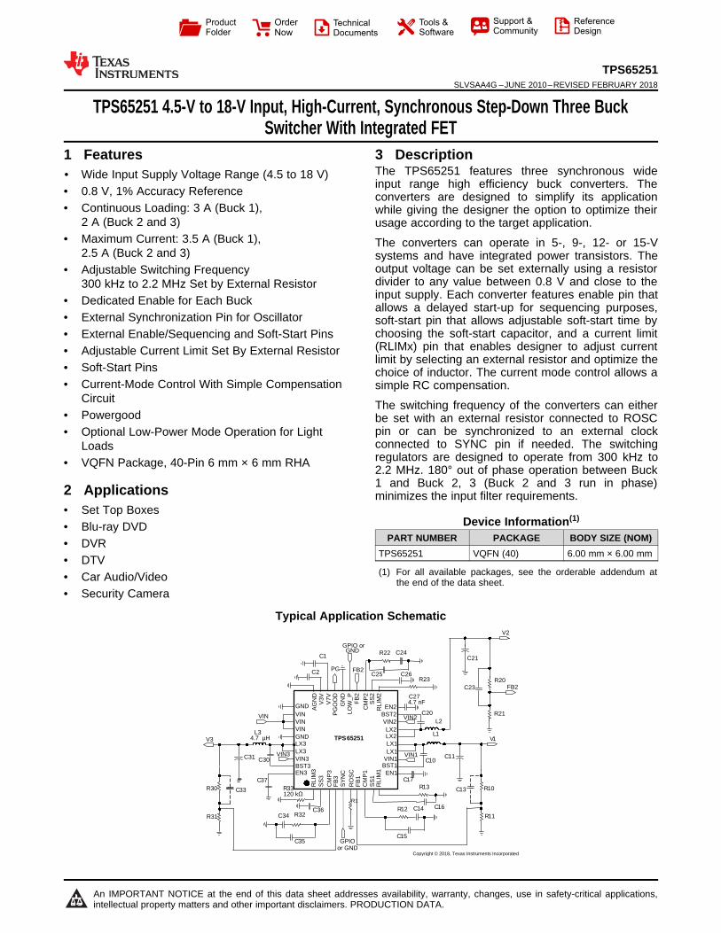
3 DescriptionThe TPS65251 features three synchronous wideinput range high efficiency buck converters. Theconverters are designed to simplify its applicationwhile giving the designer the option to optimize theirusage according to the target application.
The converters can operate in 5-, 9-, 12- or 15-Vsystems and have integrated power transistors. Theoutput voltage can be set externally using a resistordivider to any value between 0.8 V and close to theinput supply. Each converter features enable pin thatallows a delayed start-up for sequencing purposes,soft-start pin that allows adjustable soft-start time bychoosing the soft-start capacitor, and a current limit(RLIMx) pin that enables designer to adjust currentlimit by selecting an external resistor and optimize thechoice of inductor. The current mode control allows asimple RC compensation.
The switching frequency of the converters can eitherbe set with an external resistor connected to ROSCpin or can be synchronized to an external clockconnected to SYNC pin if needed. The switchingregulators are designed to operate from 300 kHz to2.2 MHz. 180° out of phase operation between Buck1 and Buck 2, 3 (Buck 2 and 3 run in phase)minimizes the input filter requirements.
Device Information(1)
PART NUMBER PACKAGE BODY SIZE (NOM)TPS65251 VQFN (40) 6.00 mm × 6.00 mm
(1) For all available packages, see the orderable addendum atthe end of the data sheet.
Typical Application Schematic
2
TPS65251SLVSAA4G –JUNE 2010–REVISED FEBRUARY 2018 www.ti.com
Product Folder Links: TPS65251
Submit Documentation Feedback Copyright © 2010–2018, Texas Instruments Incorporated
Table of Contents1 Features .................................................................. 12 Applications ........................................................... 13 Description ............................................................. 14 Revision History..................................................... 25 Description (continued)......................................... 36 Pin Configuration and Functions ......................... 37 Specifications......................................................... 5
7.1 Absolute Maximum Ratings ..................................... 57.2 ESD Ratings.............................................................. 57.3 Recommended Operating Conditions....................... 57.4 Thermal Information .................................................. 57.5 Electrical Characteristics........................................... 67.6 Typical Characteristics .............................................. 8
8 Detailed Description ............................................ 118.1 Overview ................................................................. 118.2 Functional Block Diagram ....................................... 118.3 Feature Description................................................. 12
8.4 Device Functional Modes........................................ 159 Application and Implementation ........................ 17
9.1 Application Information............................................ 179.2 Typical Application .................................................. 17
10 Power Supply Recommendations ..................... 2411 Layout................................................................... 24
11.1 Layout Guidelines ................................................. 2411.2 Layout Example .................................................... 2511.3 Power Dissipation ................................................. 25
12 Device and Documentation Support ................. 2712.1 Receiving Notification of Documentation Updates 2712.2 Community Resources.......................................... 2712.3 Trademarks ........................................................... 2712.4 Electrostatic Discharge Caution............................ 2712.5 Glossary ................................................................ 27
13 Mechanical, Packaging, and OrderableInformation ........................................................... 27
4 Revision HistoryNOTE: Page numbers for previous revisions may differ from page numbers in the current version.
Changes from Revision F (July 2015) to Revision G Page
• Changed the values for Voltage at LX1, LX2, LX3 From: MIN = –1 V, MAX = 20 V To: MIN = –3 V, MAX = 23 V inthe Absolute Maximum Ratings ............................................................................................................................................. 5
Changes from Revision E (December 2014) to Revision F Page
• Changed the MAX value for Voltage at VIN1,VIN2, VIN3, LX1, LX2, LX3 From: 18 V To: 20 V in the AbsoluteMaximum Ratings .................................................................................................................................................................. 5
• Added Community Resources ............................................................................................................................................. 27
Changes from Revision D (December 2012) to Revision E Page
• Added Pin Configuration and Functions section, ESD Ratings table, Feature Description section, Device FunctionalModes, Application and Implementation section, Power Supply Recommendations section, Layout section, Deviceand Documentation Support section, and Mechanical, Packaging, and Orderable Information section .............................. 1
(power pad connected to ground)
RL
IM3
VIN3
LX3
LX3
VIN
LX2
LX1
LX1
SS
3
CM
P3
SY
NC
1 2 3 4 5 6
11
12
13
14
15
16
17
18
19
20
7 8 9 10
CM
P1
RO
SC
FB
1
LX2
VIN2
AG
ND
V3
V
V7
V
29 28 27 26 25 24G
ND
23 22 2130
CO
MP
2
LO
W_
P
FB
2
40
39
38
37
36
35
34
33
32
31GND
VIN
VIN
PG
OO
D
BST3
EN3
VIN1
BST1
RL
IM1
SS
2
RL
IM2
EN2
BST2
SS
1
EN1
FB
3
GND
3
TPS65251www.ti.com SLVSAA4G –JUNE 2010–REVISED FEBRUARY 2018
Product Folder Links: TPS65251
Submit Documentation FeedbackCopyright © 2010–2018, Texas Instruments Incorporated
5 Description (continued)TPS65251 features a supervisor circuit that monitors each converter output. The PGOOD pin is asserted oncesequencing is done, all PG signals are reported and a selectable end of reset time lapses. The polarity of thePGOOD signal is active high.
TPS65251 also features a light load pulse skipping mode (PSM) by allowing the LOW_P pin tied to V3V. ThePSM mode allows for a reduction on the input power supplied to the system when the host processor is instandby (low-activity) mode.
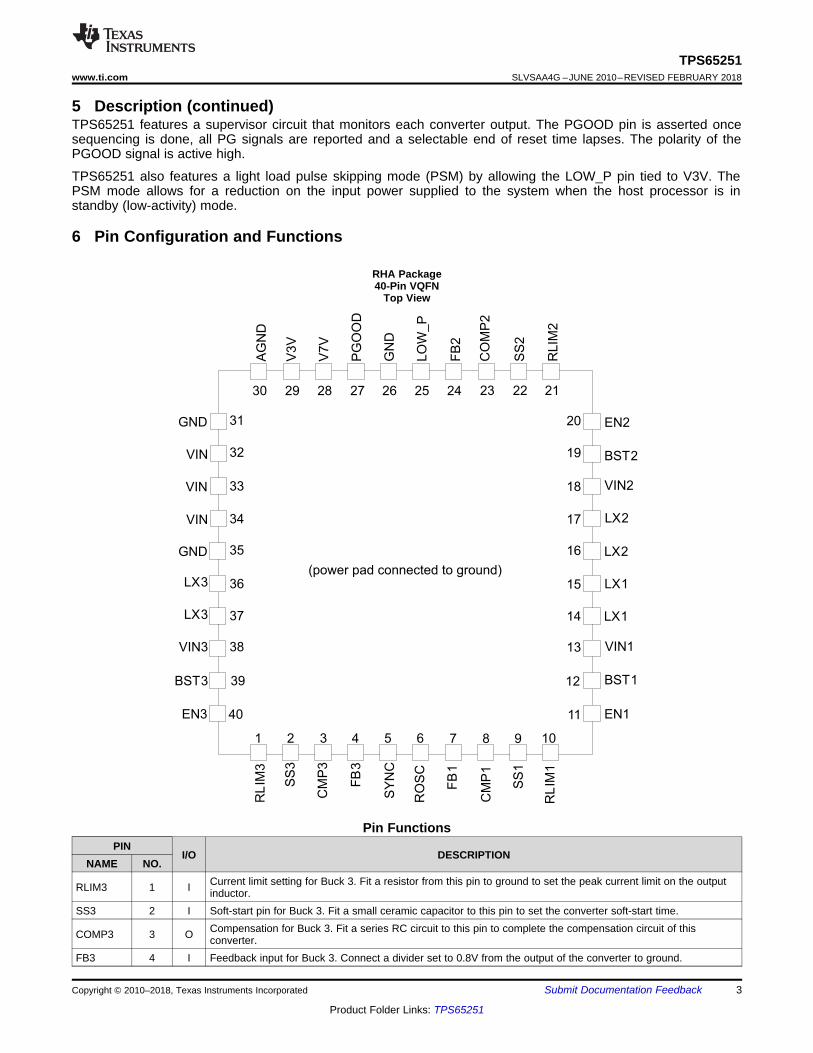
6 Pin Configuration and Functions
RHA Package40-Pin VQFN
Top View
Pin FunctionsPIN
I/O DESCRIPTIONNAME NO.
RLIM3 1 I Current limit setting for Buck 3. Fit a resistor from this pin to ground to set the peak current limit on the outputinductor.
SS3 2 I Soft-start pin for Buck 3. Fit a small ceramic capacitor to this pin to set the converter soft-start time.
COMP3 3 O Compensation for Buck 3. Fit a series RC circuit to this pin to complete the compensation circuit of thisconverter.
FB3 4 I Feedback input for Buck 3. Connect a divider set to 0.8V from the output of the converter to ground.
4
TPS65251SLVSAA4G –JUNE 2010–REVISED FEBRUARY 2018 www.ti.com
Product Folder Links: TPS65251
Submit Documentation Feedback Copyright © 2010–2018, Texas Instruments Incorporated
Pin Functions (continued)PIN
I/O DESCRIPTIONNAME NO.
SYNC 5 I Synchronous clock input. If there is a sync clock in the system, connect to the pin. When not used connect toGND.
ROSC 6 I Oscillator set. This resistor sets the frequency of internal autonomous clock. If external synchronization is usedresistor should be fitted and set to about 70% of external clock frequency.
FB1 7 I Feedback pin for Buck 1. Connect a divider set to 0.8 V from the output of the converter to ground.
COMP1 8 O Compensation pin for Buck 1. Fit a series RC circuit to this pin to complete the compensation circuit of thisconverter.
SS1 9 I Soft-start pin for Buck 1. Fit a small ceramic capacitor to this pin to set the converter soft-start time.
RLIM1 10 I Current limit setting pin for Buck 1. Fit a resistor from this pin to ground to set the peak current limit on theoutput inductor.
EN1 11 I Enable pin for Buck 1. A low level signal on this pin disables it. If pin is left open a weak internal pullup to V3Vwill allow for automatic enable. For a delayed start-up add a small ceramic capacitor from this pin to ground.
BST1 12 I Bootstrap capacitor for Buck 1. Fit a 47-nF ceramic capacitor from this pin to the switching node.VIN1 13 I Input supply for Buck 1. Fit a 10-µF ceramic capacitor close to this pin.
LX114
OSwitching node for Buck 1
15
LX216
OSwitching node for Buck 2
17VIN2 18 I Input supply for Buck 2. Fit a 10-µF ceramic capacitor close to this pin.BST2 19 I Bootstrap capacitor for Buck 2. Fit a 47-nF ceramic capacitor from this pin to the switching node.
EN2 20 I Enable pin for Buck 2. A low level signal on this pin disables it. If pin is left open a weak internal pullup to V3Vwill allow for automatic enable. For a delayed start-up add a small ceramic capacitor from this pin to ground.
RLIM2 21 I Current limit setting for Buck 2. Fit a resistor from this pin to ground to set the peak current limit on the outputinductor.
SS2 22 I Soft-start pin for Buck 2. Fit a small ceramic capacitor to this pin to set the converter soft-start time.
COMP2 23 O Compensation pin for Buck 2. Fit a series RC circuit to this pin to complete the compensation circuit of thisconverter
FB2 24 I Feedback input for Buck 2. Connect a divider set to 0.8 V from the output of the converter to ground.LOW_P 25 I Low-power operation mode (active high) input for TPS65251GND 26 Ground pin
PGOOD 27 O Powergood. Open-drain output asserted after all converters are sequenced and within regulation. Polarity isfactory selectable (active high default).
V7V 28 O Internal supply. Connect a 10-μF ceramic capacitor from this pin to ground.V3V 29 O Internal supply. Connect a 3.3-μF to 10-μF ceramic capacitor from this pin to ground.AGND 30 Analog ground. Connect all GND pins and the power pad together.GND 31 Ground pinVIN 32 I Input supplyVIN 33 I Input supplyVIN 34 I Input supplyGND 35 Ground pin
LX336
OSwitching node for Buck 3
37VIN3 38 Input supply for Buck 3. Fit a 10-µF ceramic capacitor close to this pin.BST3 39 I Bootstrap capacitor for Buck 3. Fit a 47-nF ceramic capacitor from this pin to the switching node.
EN3 40 I Enable pin for Buck 3. A low level signal on this pin disables it. If pin is left open a weak internal pullup to V3Vwill allow for automatic enable. For a delayed start-up add a small ceramic capacitor from this pin to ground.
PAD — — Power pad. Connect to ground.
5
TPS65251www.ti.com SLVSAA4G –JUNE 2010–REVISED FEBRUARY 2018
Product Folder Links: TPS65251
Submit Documentation FeedbackCopyright © 2010–2018, Texas Instruments Incorporated
(1) Stresses beyond those listed under Absolute Maximum Ratings may cause permanent damage to the device. These are stress ratingsonly, and functional operation of the device at these or any other conditions beyond those indicated under Recommended OperatingConditions is not implied. Exposure to absolute-maximum-rated conditions for extended periods may affect device reliability.
7 Specifications
7.1 Absolute Maximum Ratingsover operating free-air temperature (unless otherwise noted) (1)
MIN MAX UNITVoltage at VIN1,VIN2, VIN3, LX1, LX2, LX3 –0.3 20 VVoltage at LX1, LX2, LX3 (maximum withstand voltage transient < 10 ns) –3 23 VVoltage at BST1, BST2, BST3, referenced to Lx pin –0.3 7 VVoltage at V7V, COMP1, COMP2, COMP3 –0.3 7 VVoltage at V3V, RLIM1, RLIM2, RLIM3, EN1,EN2,EN3, SS1, SS2,SS3, FB1, FB2, FB3,PGOOD, SYNC, ROSC, LOW_P –0.3 3.6 V
Voltage at AGND, GND –0.3 0.3 VTJ Operating virtual junction temperature –40 125 °CTstg Storage temperature –55 150 °C
(1) JEDEC document JEP155 states that 500-V HBM allows safe manufacturing with a standard ESD control process.(2) JEDEC document JEP157 states that 250-V CDM allows safe manufacturing with a standard ESD control process.
7.2 ESD RatingsVALUE UNIT
V(ESD) Electrostatic dischargeHuman-body model (HBM), per ANSI/ESDA/JEDEC JS-001 (1) ±2000
VCharged-device model (CDM), per JEDEC specification JESD22-C101 (2) ±500
7.3 Recommended Operating Conditionsover operating free-air temperature range (unless otherwise noted)
MIN MAX UNITVIN Input operating voltage 4.5 18 VTJ Junction temperature –40 125 °C
(1) For more information about traditional and new thermal metrics, see the Semiconductor and IC Package Thermal Metrics applicationreport, SPRA953.
7.4 Thermal Information
THERMAL METRIC (1)TPS65251
UNITRHA (VQFN)40 PINS
RθJA Junction-to-ambient thermal resistance 30 °C/WRθJC(top) Junction-to-case (top) thermal resistance 25.3 °C/WRθJB Junction-to-board thermal resistance 73 °C/WψJT Junction-to-top characterization parameter 0.2 °C/WψJB Junction-to-board characterization parameter 7.6 °C/WRθJC(bot) Junction-to-case (bottom) thermal resistance 1.9 °C/W

6
TPS65251SLVSAA4G –JUNE 2010–REVISED FEBRUARY 2018 www.ti.com
Product Folder Links: TPS65251
Submit Documentation Feedback Copyright © 2010–2018, Texas Instruments Incorporated
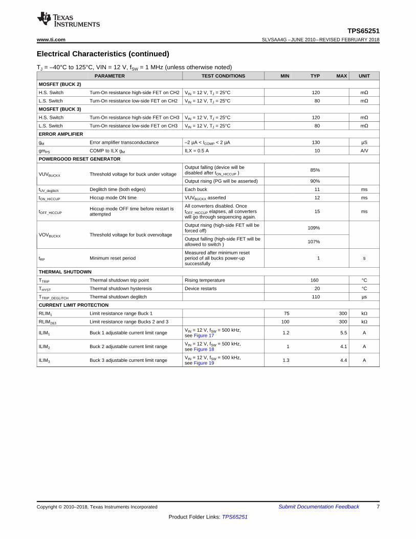
7.5 Electrical CharacteristicsTJ = –40°C to 125°C, VIN = 12 V, fSW = 1 MHz (unless otherwise noted)
PARAMETER TEST CONDITIONS MIN TYP MAX UNIT
INPUT SUPPLY UVLO AND INTERNAL SUPPLY VOLTAGE
VIN Input Voltage range 4.5 18 V
IDDSDN Shutdown EN pin = low for all converters 1.3 mA
IDDQ Quiescent, low-power disabled (Lo)
Converters enabled, no loadBuck 1 = 3.3 V, Buck 2 = 2.5 V,Buck 3 = 7.5 V,L = 4.7 µH , fSW = 800 kHz
20 mA
IDDQ_LOW_P Quiescent, low-power enabled (Hi)
Converters enabled, no loadBuck 1 = 3.3 V, Buck 2 = 2.5 V,Buck 3 = 7.5 V,L = 4.7 µH , fSW = 800 kHz
1.5 mA
UVLOVIN VIN under voltage lockoutRising VIN 4.22
VFalling VIN 4.1
UVLODEGLITCH Both edges 110 µs
V3V Internal biasing supply ILOAD = 0 mA 3.2 3.3 3.4 V
I3V Biasing supply output current VIN = 12 V 10 mA
V7V Internal biasing supply ILOAD = 0 mA 5.63 6.25 6.88 V
I7V Biasing supply output current VIN = 12 V 10 mA
V7VUVLO UVLO for internal V7V railRising V7V 3.8
VFalling V7V 3.6
V7VUVLO_DEGLITCH Falling edge 110 µs
BUCK CONVERTERS (ENABLE CIRCUIT, CURRENT LIMIT, SOFT-START, SWITCHING FREQUENCY AND SYNC CIRCUIT, LOW-POWER MODE)
VIHEnable threshold high V3p3 = 3.2 V - 3.4 V, VENX rising 1.55 1.82
VEnable high level External GPIO, VENX rising 0.66 x V3V
VILEnable threshold low V3p3 = 3.2 V - 3.4 V, VENX falling 0.98 1.24
VEnable low level External GPIO, VENX falling 0.33 x V3V
REN_DIS Enable discharge resistor –10% 2.1 10% kΩ
ICHEN Pullup current enable pin 1.1 µA
tD Discharge time enable pins Power-up 10 ms
ISS Soft-start pin current source 5 µA
FSW_BK Converter switching frequency range Set externally with resistor 0.3 2.2 MHz
RFSW Frequency setting resistor Depending on set frequency 50 600 kΩ
fSW_TOL Internal oscillator accuracy fSW = 800 kHz –10% 10%
VSYNCH External clock threshold high V3p3 = 3.3 V 1.55 V
VSYNCL External clock threshold Low V3p3 = 3.3 V 1.24 V
SYNCRANGE Synchronization range 0.2 2.2 MHz
SYNCCLK_MIN Sync signal minimum duty cycle 40%
SYNCCLK_MAX Sync signal maximum duty cycle 60%
VIHLOW_P Low-power mode threshold high V3p3 = 3.3 V, VENX rising 1.55 V
VILLOW_P Low-power mode threshold Low V3p3 = 3.3 V, VENX falling 0.98 1.24 V
FEEDBACK, REGULATION, OUTPUT STAGE
VFB Feedback voltageVIN = 12V TJ = 25°C –1% 0.8 1%
VVIN = 4.5 to 18 V –2% 0.8 2%
IFB Feedback leakage current 50 nA
tON_MINMinimum on-time(current sense blanking) 80 120 ns
VLINEREGLine regulation - DC∆VOUT/∆VINB
VINB = 4.5 to 18 V,IOUT = 1000 mA 0.5 % VOUT
VLOADREGLoad regulation - DC∆VOUT/∆IOUT
IOUT = 10 % - 90%IOUT,MAX
0.5 % VOUT/A
MOSFET (BUCK 1)
H.S. Switch Turn-On resistance high-side FET on CH1 VIN = 12 V, TJ = 25°C 95 mΩ
L.S. Switch Turn-On resistance low-side FET on CH1 VIN = 12 V, TJ = 25°C 50 mΩ
7
TPS65251www.ti.com SLVSAA4G –JUNE 2010–REVISED FEBRUARY 2018
Product Folder Links: TPS65251
Submit Documentation FeedbackCopyright © 2010–2018, Texas Instruments Incorporated
Electrical Characteristics (continued)TJ = –40°C to 125°C, VIN = 12 V, fSW = 1 MHz (unless otherwise noted)
PARAMETER TEST CONDITIONS MIN TYP MAX UNIT
MOSFET (BUCK 2)
H.S. Switch Turn-On resistance high-side FET on CH2 VIN = 12 V, TJ = 25°C 120 mΩ
L.S. Switch Turn-On resistance low-side FET on CH2 VIN = 12 V, TJ = 25°C 80 mΩ
MOSFET (BUCK 3)
H.S. Switch Turn-On resistance high-side FET on CH3 VIN = 12 V, TJ = 25°C 120 mΩ
L.S. Switch Turn-On resistance low-side FET on CH3 VIN = 12 V, TJ = 25°C 80 mΩ
ERROR AMPLIFIER
gM Error amplifier transconductance –2 µA < ICOMP < 2 µA 130 µS
gmPS COMP to ILX gM ILX = 0.5 A 10 A/V
POWERGOOD RESET GENERATOR
VUVBUCKX Threshold voltage for buck under voltageOutput falling (device will bedisabled after tON_HICCUP ) 85%
Output rising (PG will be asserted) 90%
tUV_deglitch Deglitch time (both edges) Each buck 11 ms
tON_HICCUP Hiccup mode ON time VUVBUCKX asserted 12 ms
tOFF_HICCUPHiccup mode OFF time before restart isattempted
All converters disabled. OncetOFF_HICCUP elapses, all converterswill go through sequencing again.
15 ms
VOVBUCKX Threshold voltage for buck overvoltage
Output rising (high-side FET will beforced off) 109%
Output falling (high-side FET will beallowed to switch ) 107%
tRP Minimum reset periodMeasured after minimum resetperiod of all bucks power-upsuccessfully
1 s
THERMAL SHUTDOWN
TTRIP Thermal shutdown trip point Rising temperature 160 °C
THYST Thermal shutdown hysteresis Device restarts 20 °C
TTRIP_DEGLITCH Thermal shutdown deglitch 110 µs
CURRENT LIMIT PROTECTION
RLIM1 Limit resistance range Buck 1 75 300 kΩ
RLIM2&3 Limit resistance range Bucks 2 and 3 100 300 kΩ
ILIM1 Buck 1 adjustable current limit range VIN = 12 V, fSW = 500 kHz,see Figure 17 1.2 5.5 A
ILIM2 Buck 2 adjustable current limit range VIN = 12 V, fSW = 500 kHz,see Figure 18 1 4.1 A
ILIM3 Buck 3 adjustable current limit range VIN = 12 V, fSW = 500 kHz,see Figure 19 1.3 4.4 A
8
TPS65251SLVSAA4G –JUNE 2010–REVISED FEBRUARY 2018 www.ti.com
Product Folder Links: TPS65251
Submit Documentation Feedback Copyright © 2010–2018, Texas Instruments Incorporated
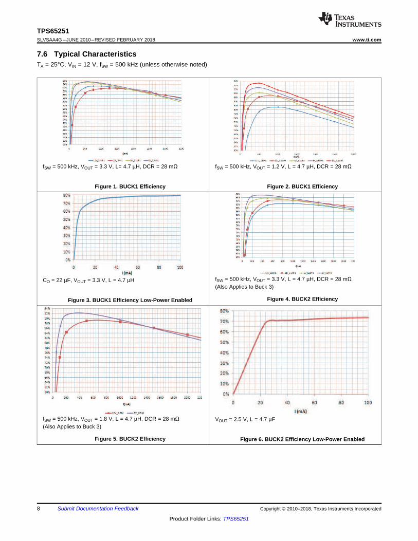
7.6 Typical CharacteristicsTA = 25°C, VIN = 12 V, fSW = 500 kHz (unless otherwise noted)
fSW = 500 kHz, VOUT = 3.3 V, L= 4.7 µH, DCR = 28 mΩ
Figure 1. BUCK1 Efficiency
fSW = 500 kHz, VOUT = 1.2 V, L = 4.7 µH, DCR = 28 mΩ
Figure 2. BUCK1 Efficiency
CO = 22 µF, VOUT = 3.3 V, L = 4.7 µH
Figure 3. BUCK1 Efficiency Low-Power Enabled
fSW = 500 kHz, VOUT = 3.3 V, L = 4.7 µH, DCR = 28 mΩ(Also Applies to Buck 3)
Figure 4. BUCK2 Efficiency
fSW = 500 kHz, VOUT = 1.8 V, L = 4.7 µH, DCR = 28 mΩ(Also Applies to Buck 3)
Figure 5. BUCK2 Efficiency
VOUT = 2.5 V, L = 4.7 µF
Figure 6. BUCK2 Efficiency Low-Power Enabled
9
TPS65251www.ti.com SLVSAA4G –JUNE 2010–REVISED FEBRUARY 2018
Product Folder Links: TPS65251
Submit Documentation FeedbackCopyright © 2010–2018, Texas Instruments Incorporated
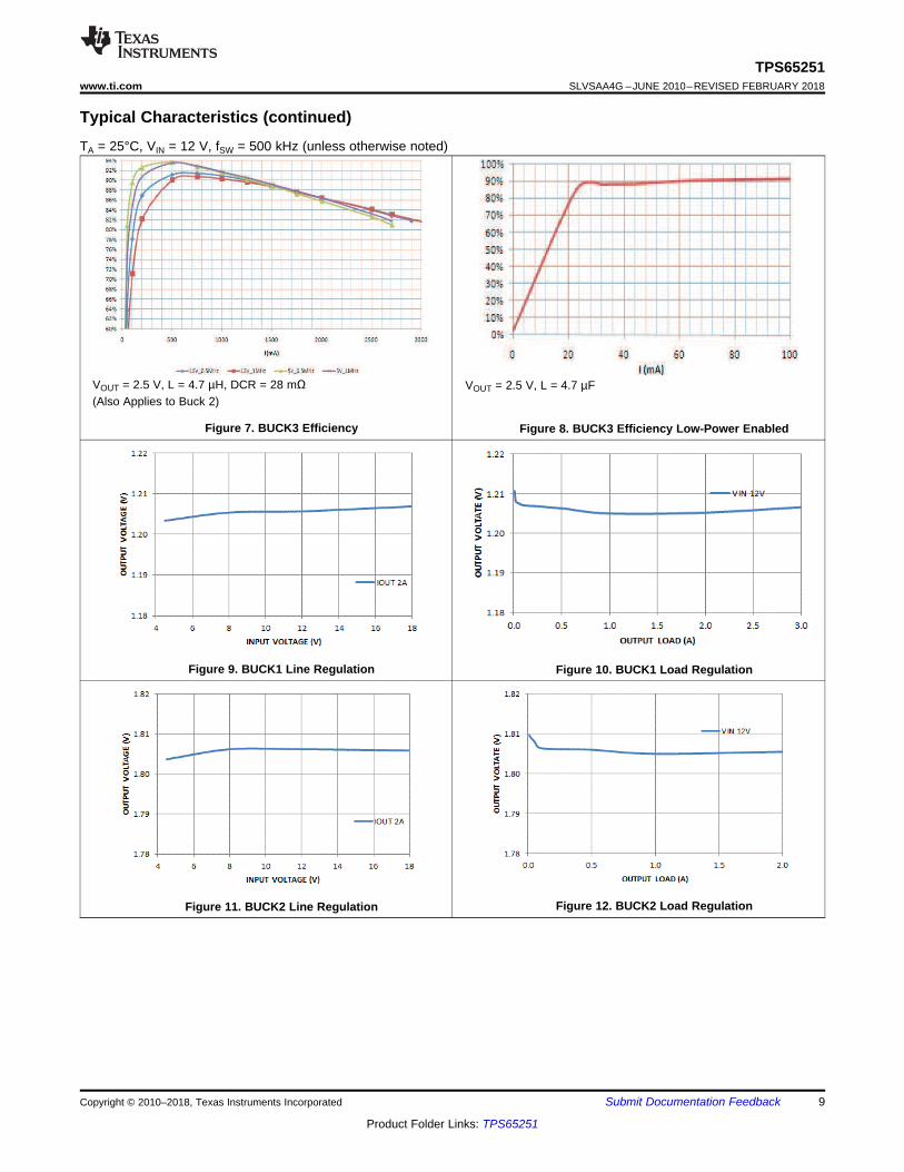
Typical Characteristics (continued)TA = 25°C, VIN = 12 V, fSW = 500 kHz (unless otherwise noted)
VOUT = 2.5 V, L = 4.7 µH, DCR = 28 mΩ(Also Applies to Buck 2)
Figure 7. BUCK3 Efficiency
VOUT = 2.5 V, L = 4.7 µF
Figure 8. BUCK3 Efficiency Low-Power Enabled
Figure 9. BUCK1 Line Regulation Figure 10. BUCK1 Load Regulation
Figure 11. BUCK2 Line Regulation Figure 12. BUCK2 Load Regulation

10
TPS65251SLVSAA4G –JUNE 2010–REVISED FEBRUARY 2018 www.ti.com
Product Folder Links: TPS65251
Submit Documentation Feedback Copyright © 2010–2018, Texas Instruments Incorporated
Typical Characteristics (continued)TA = 25°C, VIN = 12 V, fSW = 500 kHz (unless otherwise noted)
Figure 13. BUCK3 Line Regulation Figure 14. BUCK3 Load Regulation
OSC
EN3
12V DC Supply
from enable logic
INTERNALVOLTAGE RAILS
V3V
V7V
Vout BUCK1LX1
LX1
FB1
COMP1
BST1
BUCK1
Vout BUCK2LX2
LX2
FB2
COMP2
BST2
BUCK2
Vout BUCK3LX3
LX3
FB3
COMP3
BST3
BUCK3
EN2from enable logic
EN1from enable logic
SS2
SS1
SS3
VIN1
VIN2
VIN3
Rlim1
ROSC
AGND
PG Generator
PGOOD
SYNC
Rlim2
Rlim3
PFM mode LOW_P
VIN
GND
Copyright © 2018, Texas Instruments Incorporated
11
TPS65251www.ti.com SLVSAA4G –JUNE 2010–REVISED FEBRUARY 2018
Product Folder Links: TPS65251
Submit Documentation FeedbackCopyright © 2010–2018, Texas Instruments Incorporated
8 Detailed Description
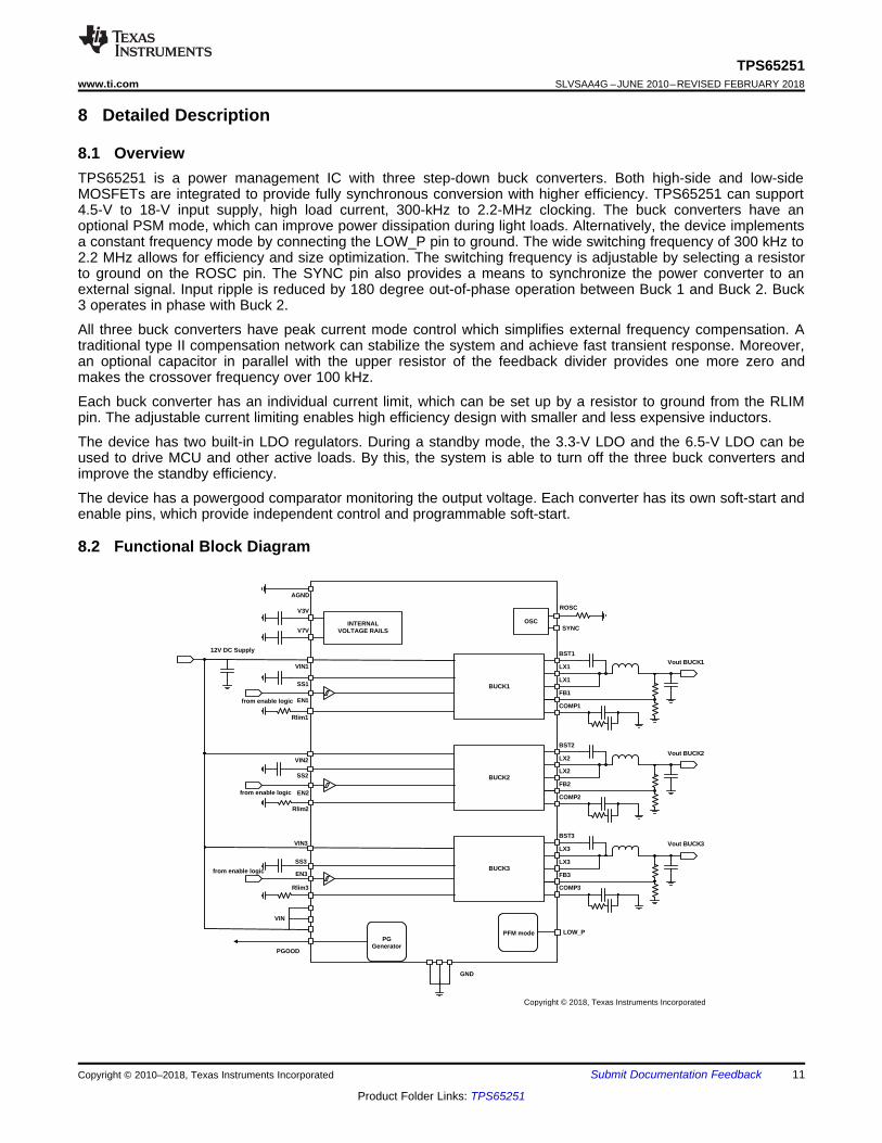
8.1 OverviewTPS65251 is a power management IC with three step-down buck converters. Both high-side and low-sideMOSFETs are integrated to provide fully synchronous conversion with higher efficiency. TPS65251 can support4.5-V to 18-V input supply, high load current, 300-kHz to 2.2-MHz clocking. The buck converters have anoptional PSM mode, which can improve power dissipation during light loads. Alternatively, the device implementsa constant frequency mode by connecting the LOW_P pin to ground. The wide switching frequency of 300 kHz to2.2 MHz allows for efficiency and size optimization. The switching frequency is adjustable by selecting a resistorto ground on the ROSC pin. The SYNC pin also provides a means to synchronize the power converter to anexternal signal. Input ripple is reduced by 180 degree out-of-phase operation between Buck 1 and Buck 2. Buck3 operates in phase with Buck 2.
All three buck converters have peak current mode control which simplifies external frequency compensation. Atraditional type II compensation network can stabilize the system and achieve fast transient response. Moreover,an optional capacitor in parallel with the upper resistor of the feedback divider provides one more zero andmakes the crossover frequency over 100 kHz.
Each buck converter has an individual current limit, which can be set up by a resistor to ground from the RLIMpin. The adjustable current limiting enables high efficiency design with smaller and less expensive inductors.
The device has two built-in LDO regulators. During a standby mode, the 3.3-V LDO and the 6.5-V LDO can beused to drive MCU and other active loads. By this, the system is able to turn off the three buck converters andimprove the standby efficiency.
The device has a powergood comparator monitoring the output voltage. Each converter has its own soft-start andenable pins, which provide independent control and programmable soft-start.
8.2 Functional Block Diagram
±OSC5 N ¦0+]: u
12
TPS65251SLVSAA4G –JUNE 2010–REVISED FEBRUARY 2018 www.ti.com
Product Folder Links: TPS65251
Submit Documentation Feedback Copyright © 2010–2018, Texas Instruments Incorporated
8.3 Feature Description
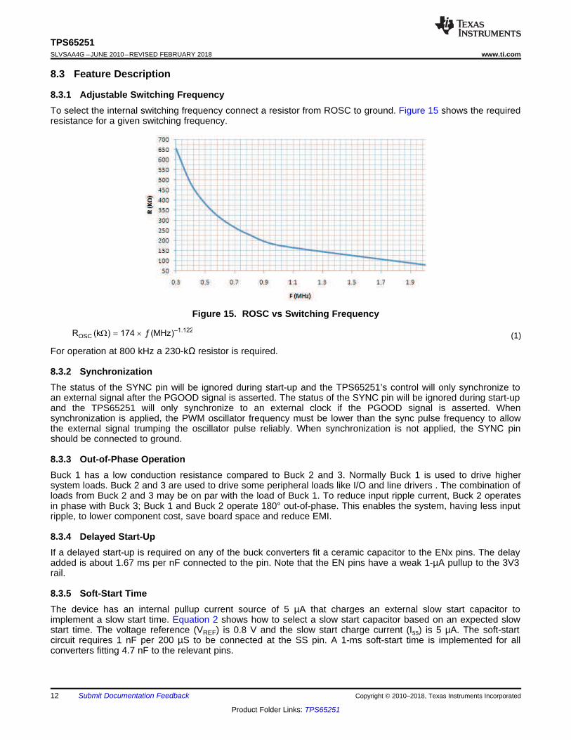
8.3.1 Adjustable Switching FrequencyTo select the internal switching frequency connect a resistor from ROSC to ground. Figure 15 shows the requiredresistance for a given switching frequency.
Figure 15. ROSC vs Switching Frequency
(1)
For operation at 800 kHz a 230-kΩ resistor is required.
8.3.2 SynchronizationThe status of the SYNC pin will be ignored during start-up and the TPS65251’s control will only synchronize toan external signal after the PGOOD signal is asserted. The status of the SYNC pin will be ignored during start-upand the TPS65251 will only synchronize to an external clock if the PGOOD signal is asserted. Whensynchronization is applied, the PWM oscillator frequency must be lower than the sync pulse frequency to allowthe external signal trumping the oscillator pulse reliably. When synchronization is not applied, the SYNC pinshould be connected to ground.
8.3.3 Out-of-Phase OperationBuck 1 has a low conduction resistance compared to Buck 2 and 3. Normally Buck 1 is used to drive highersystem loads. Buck 2 and 3 are used to drive some peripheral loads like I/O and line drivers . The combination ofloads from Buck 2 and 3 may be on par with the load of Buck 1. To reduce input ripple current, Buck 2 operatesin phase with Buck 3; Buck 1 and Buck 2 operate 180° out-of-phase. This enables the system, having less inputripple, to lower component cost, save board space and reduce EMI.
8.3.4 Delayed Start-UpIf a delayed start-up is required on any of the buck converters fit a ceramic capacitor to the ENx pins. The delayadded is about 1.67 ms per nF connected to the pin. Note that the EN pins have a weak 1-µA pullup to the 3V3rail.
8.3.5 Soft-Start TimeThe device has an internal pullup current source of 5 µA that charges an external slow start capacitor toimplement a slow start time. Equation 2 shows how to select a slow start capacitor based on an expected slowstart time. The voltage reference (VREF) is 0.8 V and the slow start charge current (Iss) is 5 µA. The soft-startcircuit requires 1 nF per 200 µS to be connected at the SS pin. A 1-ms soft-start time is implemented for allconverters fitting 4.7 nF to the relevant pins.

FB
0.8V
Vo
+
-
TPS65251
R1
R2
O
0.8 VR2 R1
9 ± 9
§ · u ¨ ¸
© ¹
SSSS REF
SS
C (nF)t (ms) V (V)
I (µA)
§ · u ¨ ¸
© ¹
13
TPS65251www.ti.com SLVSAA4G –JUNE 2010–REVISED FEBRUARY 2018
Product Folder Links: TPS65251
Submit Documentation FeedbackCopyright © 2010–2018, Texas Instruments Incorporated
Feature Description (continued)
(2)
8.3.6 Adjusting the Output VoltageThe output voltage is set with a resistor divider from the output node to the FB pin. TI recommends to use 1%tolerance or better divider resistors. In order to improve efficiency at light load, start with 40.2 kΩ for the R1resistor and use the Equation 3 to calculate R2.
(3)
Figure 16. Voltage Divider Circuit
8.3.7 Input CapacitorUse 10-µF X7R/X5R ceramic capacitors at the input of the converter inputs. These capacitors should beconnected as close as physically possible to the input pins of the converters.
8.3.8 Bootstrap CapacitorThe device has three integrated boot regulators and requires a small ceramic capacitor between the BST and LXpin to provide the gate drive voltage for the high-side MOSFET. The value of the ceramic capacitor should be0.047 µF. A ceramic capacitor with an X7R or X5R grade dielectric is recommended because of the stablecharacteristics over temperature and voltage.
8.3.9 Error AmplifierThe device has a transconductance error amplifier. The frequency compensation network is connected betweenthe COMP pin and ground.
8.3.10 Loop CompensationTPS65251 is a current mode control DC - DC converter. The error amplifier is a transconductance amplifier witha of 130 µA/V.
8.3.11 Slope CompensationThe device has a built-in slope compensation ramp. The slope compensation can prevent subharmonicoscillations in peak current mode control.
8.3.12 PowergoodThe PGOOD pin is an open-drain output. The PGOOD pin is pulled low when any buck converter is pulled below85% of the nominal output voltage. The PGOOD is pulled up when all three buck converters’ outputs are morethan 90% of its nominal output voltage and reset time of 1 second elapses. The polarity of the PGOOD is activehigh.
14
TPS65251SLVSAA4G –JUNE 2010–REVISED FEBRUARY 2018 www.ti.com
Product Folder Links: TPS65251
Submit Documentation Feedback Copyright © 2010–2018, Texas Instruments Incorporated
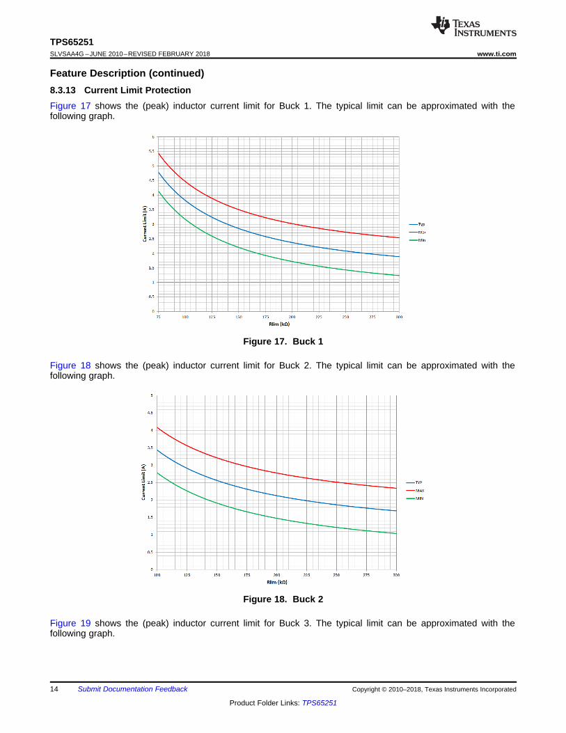
Feature Description (continued)8.3.13 Current Limit ProtectionFigure 17 shows the (peak) inductor current limit for Buck 1. The typical limit can be approximated with thefollowing graph.
Figure 17. Buck 1
Figure 18 shows the (peak) inductor current limit for Buck 2. The typical limit can be approximated with thefollowing graph.
Figure 18. Buck 2
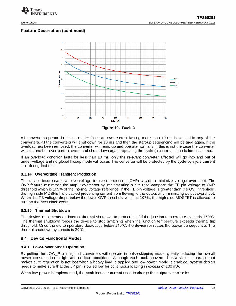
Figure 19 shows the (peak) inductor current limit for Buck 3. The typical limit can be approximated with thefollowing graph.
15
TPS65251www.ti.com SLVSAA4G –JUNE 2010–REVISED FEBRUARY 2018
Product Folder Links: TPS65251
Submit Documentation FeedbackCopyright © 2010–2018, Texas Instruments Incorporated
Feature Description (continued)
Figure 19. Buck 3
All converters operate in hiccup mode: Once an over-current lasting more than 10 ms is sensed in any of theconverters, all the converters will shut down for 10 ms and then the start-up sequencing will be tried again. If theoverload has been removed, the converter will ramp up and operate normally. If this is not the case the converterwill see another over-current event and shuts-down again repeating the cycle (hiccup) until the failure is cleared.
If an overload condition lasts for less than 10 ms, only the relevant converter affected will go into and out ofunder-voltage and no global hiccup mode will occur. The converter will be protected by the cycle-by-cycle currentlimit during that time.
8.3.14 Overvoltage Transient ProtectionThe device incorporates an overvoltage transient protection (OVP) circuit to minimize voltage overshoot. TheOVP feature minimizes the output overshoot by implementing a circuit to compare the FB pin voltage to OVPthreshold which is 109% of the internal voltage reference. If the FB pin voltage is greater than the OVP threshold,the high-side MOSFET is disabled preventing current from flowing to the output and minimizing output overshoot.When the FB voltage drops below the lower OVP threshold which is 107%, the high-side MOSFET is allowed toturn on the next clock cycle.
8.3.15 Thermal ShutdownThe device implements an internal thermal shutdown to protect itself if the junction temperature exceeds 160°C.The thermal shutdown forces the device to stop switching when the junction temperature exceeds thermal tripthreshold. Once the die temperature decreases below 140°C, the device reinitiates the power-up sequence. Thethermal shutdown hysteresis is 20°C.
8.4 Device Functional Modes
8.4.1 Low-Power Mode OperationBy pulling the LOW_P pin high all converters will operate in pulse-skipping mode, greatly reducing the overallpower consumption at light and no load conditions. Although each buck converter has a skip comparator thatmakes sure regulation is not lost when a heavy load is applied and low-power mode is enabled, system designneeds to make sure that the LP pin is pulled low for continuous loading in excess of 100 mA.
When low-power is implemented, the peak inductor current used to charge the output capacitor is:

VOUT
VOUT_PK
V = V +OUT_PK OUT
DVOUT¾
2
DV =OUT
1¾C
·(L I· LIMIT
2
¾2
·VIN¾
V V - VOUT IN OUT· ( )-
ILOAD¾fSLEEP_CLK
)
I = TLIMIT SLEEP_CLK0.25 · ·
V - VIN OUT¾
L
16
TPS65251SLVSAA4G –JUNE 2010–REVISED FEBRUARY 2018 www.ti.com
Product Folder Links: TPS65251
Submit Documentation Feedback Copyright © 2010–2018, Texas Instruments Incorporated
Device Functional Modes (continued)
(4)
Where TSLEEP_CLK is half of the converter switching period, 2/fSW.
The size of the additional ripple added to the output is:
(5)
And the peak output voltage during low-power operation is:
(6)
Figure 20. Peak Output Voltage During Low-Power Operation
TPS65251
C25100pF
R2220K
C244700pF
R2040.2K
R2132K
1.8V 2A
L24.7uH
GND
VIN
LX3
VIN
LX3
GND
C234.7nF
BST3VIN3
EN3
FB
1
SS
1
SY
NC
CM
P1
RO
SC
RL
IM1
CM
P3
RL
IM3
FB
3
SS
3
LX2
BST2
LX1
VIN2
LX2
EN2
VIN1
EN1
LX1
BST1
CM
P2
GN
D
FB
2LO
W_
P
SS
2
V7
V
AG
ND
PG
OO
D
V3
V
C1122uF
R1040.2K
R1180.6K
1.2V 3AL1
4.7uH
C134.7nF
R13100K
C15100pF
R1220K
C144700pF
V2
V1
VIN1C1047nF
C274.7nF
C174.7nF
VIN
C35100pF
R3220K
C344700pF
C364.7nF
R1383K
C264.7nF
C2122uF
FB2
FB2LPPG
C110uF
C23.3uF
C374.7nF
C3122uF
R3040.2K
R3112.7K
3.3V 2A
C334.7nF
V3
C3047nF
VIN3
VINC2047nFVIN2
C164.7nF
L34.7uH
R23150K
RLI
M2
R33120K
Copyright © 2018, Texas Instruments Incorporated
17
TPS65251www.ti.com SLVSAA4G –JUNE 2010–REVISED FEBRUARY 2018
Product Folder Links: TPS65251
Submit Documentation FeedbackCopyright © 2010–2018, Texas Instruments Incorporated
9 Application and Implementation
NOTEInformation in the following applications sections is not part of the TI componentspecification, and TI does not warrant its accuracy or completeness. TI’s customers areresponsible for determining suitability of components for their purposes. Customers shouldvalidate and test their design implementation to confirm system functionality.
9.1 Application InformationThe device is triple synchronous step down dc/dc converter. It is typically used to convert a higher dc voltage tolower dc voltages with continuous available output current of 3A/2A/2A.
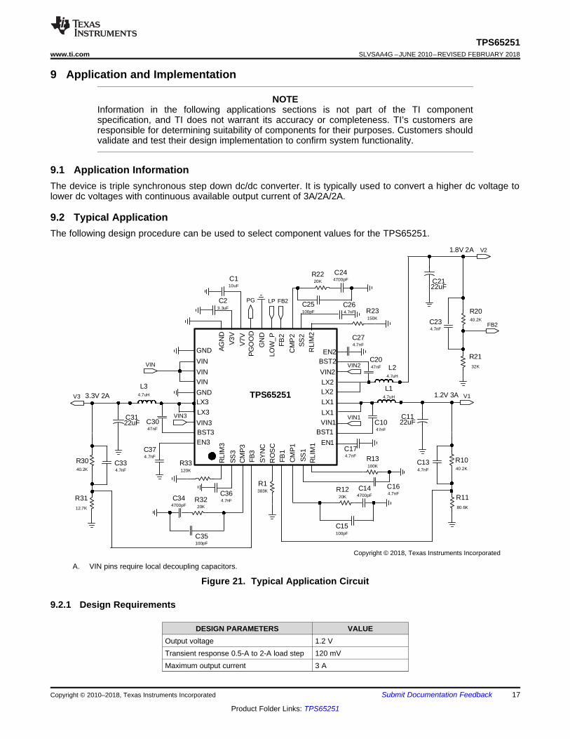
9.2 Typical ApplicationThe following design procedure can be used to select component values for the TPS65251.
A. VIN pins require local decoupling capacitors.
Figure 21. Typical Application Circuit
9.2.1 Design Requirements
DESIGN PARAMETERS VALUEOutput voltage 1.2 VTransient response 0.5-A to 2-A load step 120 mVMaximum output current 3 A

c O OC
M ps
2 ƒ V CR
g Vref gm
p ´ ´ ´
=
´ ´
c OC
M ps
2 ƒ CR
g gm
p ´ ´
=
´
Current Sense
I/V Gain
V.Vref 80=
oV
Li
ESRR
1R
2R
cR
oC
cC
RollC
ffC
LR
ug M 130=
COMPx
FBx
Gm=10A/V
18
TPS65251SLVSAA4G –JUNE 2010–REVISED FEBRUARY 2018 www.ti.com
Product Folder Links: TPS65251
Submit Documentation Feedback Copyright © 2010–2018, Texas Instruments Incorporated
DESIGN PARAMETERS VALUEInput voltage 12 V nom, 9.6 V to 14.4 VOutput voltage ripple < 30 mV p-pSwitching frequency 500 kHz
9.2.2 Detailed Design Procedure
9.2.2.1 Loop Compensation CircuitA typical compensation circuit could be type II (Rc and Cc) to have a phase margin between 60 and 90 degrees,or type III (Rc, Cc and Cff) to improve the converter transient response. CRoll adds a high frequency pole toattenuate high-frequency noise when needed. It may also prevent noise coupling from other rails if there ispossibility of cross coupling in between rails when layout is very compact.
Figure 22. Loop Compensation
To calculate the external compensation components use Table 1:
Table 1. Design Guideline for the Loop CompensationTYPE II CIRCUIT TYPE III CIRCUIT
Select switching frequency that is appropriate forapplication depending on L, C sizes, output ripple, EMIconcerns and etc. Switching frequencies between 500 kHzand 1 MHz give best trade off between performance andcost. When using smaller L and Cs, switching frequencycan be increased. To optimize efficiency, switchingfrequency can be lowered.
Type III circuit recommended forswitching frequencies higher than
500 kHz.
Select cross over frequency (fc) to be less than 1/5 to 1/10of switching frequency.
Suggestedfc = fs/10
Suggestedfc = fs/10
Set and calculate Rc.(7) (8)

2
OUT o
out
I LCo
V Vout
D ´>
´ D
IrippleILpeak Iout
2= +
22 1 Vo (Vinmax Vo)
ILrms Io12 Vinmax Lo ƒsw
æ ö´ -= + ´ ç ÷
´ ´è ø
Vin Vout VoutIripple
Lo Vin fsw
-
= ´
´
ind
Vin Vout VoutLo
Io K Vin ƒsw
-
= ´
´ ´
¦¦¦¦
1C
¦] 5
u S u u
RollC Roll
1¦S
2 R C
u S u u
sr ORoll
C
Re CC
R
u
sr ORoll
C
Re CC
R
u
O L
1¦S
C R 2
u u S
Lc
c
R CoC
R
´
=L
c
c
R CoC
R
´
=
19
TPS65251www.ti.com SLVSAA4G –JUNE 2010–REVISED FEBRUARY 2018
Product Folder Links: TPS65251
Submit Documentation FeedbackCopyright © 2010–2018, Texas Instruments Incorporated
Table 1. Design Guideline for the Loop Compensation (continued)TYPE II CIRCUIT TYPE III CIRCUIT
Calculate Cc by placing a compensation zero at or beforethe converter dominant pole
(9)(10) (11)
Add CRoll if needed to remove large signal coupling to highimpedance COMP node. Make sure that
(12)is at least twice the cross over frequency.
(13) (14)
Calculate Cff compensation zero at low frequency to boostthe phase margin at the crossover frequency. Make surethat the zero frequency (fzff is smaller than soft-startequivalent frequency (1/Tss).
NA
(15)
9.2.2.2 Selecting the Switching FrequencyThe first step is to decide on a switching frequency for the regulator. Typically, you will want to choose thehighest switching frequency possible since this will produce the smallest solution size. The high switchingfrequency allows for lower valued inductors and smaller output capacitors compared to a power supply thatswitches at a lower frequency. However, the highest switching frequency causes extra switching losses, whichhurt the converter’s performance. The converter is capable of running from 300 kHz to 2.2 MHz. Unless a smallsolution size is an ultimate goal, a moderate switching frequency of 500 kHz is selected to achieve both a smallsolution size and a high efficiency operation. Using Figure 15, R1 is determined to be 383 kΩ
9.2.2.3 Output Inductor SelectionTo calculate the value of the output inductor, use Equation 16. KIND is a coefficient that represents the amountof inductor ripple current relative to the maximum output current. In general, KIND is normally from 0.1 to 0.3 forthe majority of applications.
For this design example, use KIND = 0.2 and the inductor value is calculated to be 3.6 µH. For this design, anearest standard value was chosen: 4.7 µH. For the output filter inductor, it is important that the RMS currentand saturation current ratings not be exceeded. The RMS and peak inductor current can be found fromEquation 17 and Equation 18.
(16)
(17)
(18)
(19)
9.2.2.4 Output CapacitorThere are two primary considerations for selecting the value of the output capacitor. The output capacitors areselected to meet load transient and output ripple’s requirements.
Equation 20 gives the minimum output capacitance to meet the transient specification. For this example,LO = 4.7 µH, ΔIOUT = 1.5 A – 0.75 A = 0.75 A and ΔVOUT = 120 mV. Using these numbers gives a minimumcapacitance of 18 µF. A standard 22-µF ceramic capacitor is chose in the design.
(20)
Tss(ms) Iss(µA)Css(nF)
Vref(V)
´
=
Ioutmax 0.25Vin
Cin ƒsw
´D =
´
( )Vinmin VoutVoutIcirms Iout
Vinmin Vinmin
-= ´ ´
1 1Co
Vripple8 ƒsw
Iripple
> ´
´
20
TPS65251SLVSAA4G –JUNE 2010–REVISED FEBRUARY 2018 www.ti.com
Product Folder Links: TPS65251
Submit Documentation Feedback Copyright © 2010–2018, Texas Instruments Incorporated
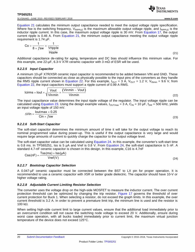
Equation 21 calculates the minimum output capacitance needed to meet the output voltage ripple specification.Where fsw is the switching frequency, VRIPPLE is the maximum allowable output voltage ripple, and IRIPPLE is theinductor ripple current. In this case, the maximum output voltage ripple is 30 mV. From Equation 17, the outputcurrent ripple is 0.46 A. From Equation 21, the minimum output capacitance meeting the output voltage ripplerequirement is 1.74 µF.
(21)
Additional capacitance de-rating for aging, temperature and DC bias should influence this minimum value. Forthis example, one 22-µF, 6.3-V X7R ceramic capacitor with 3 mΩ of ESR will be used.
9.2.2.5 Input CapacitorA minimum 10-µF X7R/X5R ceramic input capacitor is recommended to be added between VIN and GND. Thesecapacitors should be connected as close as physically possible to the input pins of the converters as they handlethe RMS ripple current shown in Equation 22. For this example, IOUT = 3 A, VOUT = 1.2 V, VINmin = 9.6 V, fromEquation 22, the input capacitors must support a ripple current of 0.99 A RMS.
(22)
The input capacitance value determines the input ripple voltage of the regulator. The input voltage ripple can becalculated using Equation 23. Using the design example values, IOUTmax = 3 A, CIN = 10 µF, fSW = 500 kHz, yieldsan input voltage ripple of 150 mV.
(23)
9.2.2.6 Soft-Start CapacitorThe soft-start capacitor determines the minimum amount of time it will take for the output voltage to reach itsnominal programmed value during power-up. This is useful if the output capacitance is very large and wouldrequire large amounts of current to quickly charge the capacitor to the output voltage level.
The soft-start capacitor value can be calculated using Equation 24. In this example, the converter’s soft-start timeis 0.8 ms. In TPS65251, Iss is 5 µA and Vref is 0.8 V. From Equation 24, the soft-start capacitance is 5 nF. Astandard 4.7-nF ceramic capacitor is chosen in this design. In this example, C16 is 4.7nF
(24)
9.2.2.7 Bootstrap Capacitor SelectionA 0.047-µF ceramic capacitor must be connected between the BST to LX pin for proper operation. It isrecommended to use a ceramic capacitor with X5R or better grade dielectric. The capacitor should have 10-V orhigher voltage rating.
9.2.2.8 Adjustable Current Limiting Resistor SelectionThe converter uses the voltage drop on the high-side MOSFET to measure the inductor current. The over currentprotection threshold can be optimized by changing the trip resistor. Figure 17 governs the threshold of overcurrent protection for Buck 1. When selecting a resistor, do not exceed the graph limits. In this example, the overcurrent threshold is 3.2 A. In order to prevent a premature limit trip, the minimum line is used and the resistor is100 kΩ.
When setting high-side current limit to large current values, ensure that the additional load immediately prior toan overcurrent condition will not cause the switching node voltage to exceed 20 V. Additionally, ensure duringworst case operation, with all bucks loaded immediately prior to current limit, the maximum virtual junctiontemperature of the device does not exceed 125°C.

M ps
2 ƒc Vo CoR12
g Vref gm
p ´ ´ ´
=
´ ´
Vout VrefR11 R10
Vref
-
= ´
21
TPS65251www.ti.com SLVSAA4G –JUNE 2010–REVISED FEBRUARY 2018
Product Folder Links: TPS65251
Submit Documentation FeedbackCopyright © 2010–2018, Texas Instruments Incorporated
9.2.2.9 Output Voltage and Feedback Resistors SelectionFor the example design, 40.2 kΩ was selected for R10. Vout is 1.2 V, Vref = 0.8 V. Using Equation 25, R11 iscalculated as 80.4 kΩ. A standard 80.6-kΩ resistor is chose in this design.
(25)
9.2.2.10 CompensationA type-II compensation circuit is adequate for the converter to have a phase margin between 60 and 90 degrees.The following equations show the procedure of designing a peak current mode control dc/dc converter.
The compensation design takes the following steps:1. Set up the anticipated cross-over frequency. In this example, the anticipated cross-over frequency (fc) is 65
kHz. The power stage gain (gmPS ) is 10 A/V and the GM amplifier gain (gM ) is 130 µA/V.
(26)2. Place compensation zero at low frequency to boost the phase margin at the crossover frequency. From the
procedures above, the compensation network includes a 20-kΩ resistor (R12) and a 4700-pF capacitor (C1).3. An additional pole can be added to attenuate high frequency noise.
From the procedures above, the compensation network includes a 20-kΩ resistor (R12) and a 4700-pF capacitor(C14).
9.2.2.11 3.3-V and 6.5-V LDO RegulatorsThe following ceramic capacitor (X7R/X5R) should be connected as close as possible to the described pins:• 10 µF for V7V pin 28• 3.3 µF to 10 µF for V3V pin 29
9.2.3 Application Curves
Figure 23. BUCK1 Start-UpLO = 4.7 µH, CO = 22 µF, VOUT = 3.3 V, 2 A
Figure 24. BUCK1 RippleVOUT = 3.3 V, 1.5 A, fSW = 800 kHz, 20 mV/div
22
TPS65251SLVSAA4G –JUNE 2010–REVISED FEBRUARY 2018 www.ti.com
Product Folder Links: TPS65251
Submit Documentation Feedback Copyright © 2010–2018, Texas Instruments Incorporated
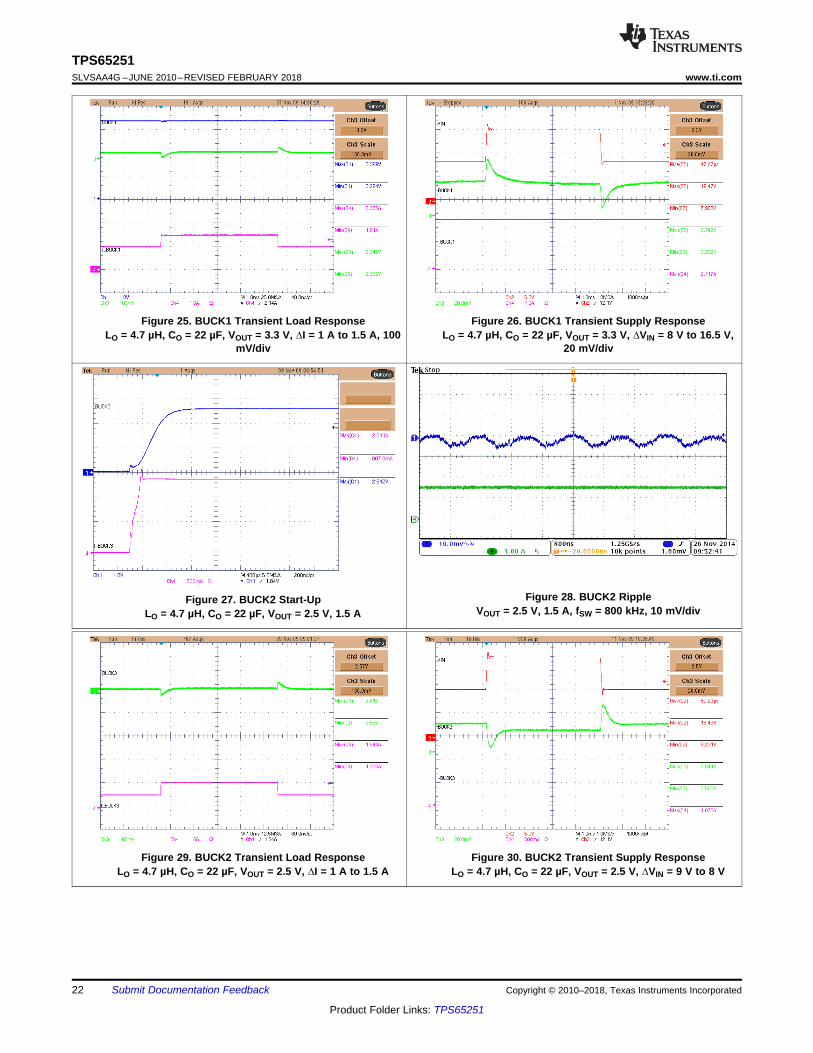
Figure 25. BUCK1 Transient Load ResponseLO = 4.7 µH, CO = 22 µF, VOUT = 3.3 V, ∆I = 1 A to 1.5 A, 100
mV/div
Figure 26. BUCK1 Transient Supply ResponseLO = 4.7 µH, CO = 22 µF, VOUT = 3.3 V, ∆VIN = 8 V to 16.5 V,
20 mV/div
Figure 27. BUCK2 Start-UpLO = 4.7 µH, CO = 22 µF, VOUT = 2.5 V, 1.5 A
Figure 28. BUCK2 RippleVOUT = 2.5 V, 1.5 A, fSW = 800 kHz, 10 mV/div
Figure 29. BUCK2 Transient Load ResponseLO = 4.7 µH, CO = 22 µF, VOUT = 2.5 V, ∆I = 1 A to 1.5 A
Figure 30. BUCK2 Transient Supply ResponseLO = 4.7 µH, CO = 22 µF, VOUT = 2.5 V, ∆VIN = 9 V to 8 V
23
TPS65251www.ti.com SLVSAA4G –JUNE 2010–REVISED FEBRUARY 2018
Product Folder Links: TPS65251
Submit Documentation FeedbackCopyright © 2010–2018, Texas Instruments Incorporated
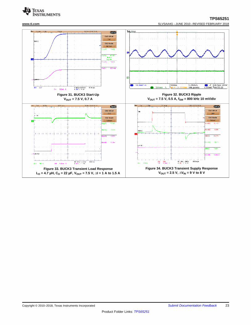
Figure 31. BUCK3 Start-UpVOUT = 7.5 V, 0.7 A
Figure 32. BUCK3 RippleVOUT = 7.5 V, 0.5 A, fSW = 800 kHz 10 mV/div
Figure 33. BUCK3 Transient Load ResponseLO = 4.7 µH, CO = 22 µF, VOUT = 7.5 V, ∆I = 1 A to 1.5 A
Figure 34. BUCK3 Transient Supply ResponseVOUT = 2.5 V, ∆VIN = 9 V to 8 V
24
TPS65251SLVSAA4G –JUNE 2010–REVISED FEBRUARY 2018 www.ti.com
Product Folder Links: TPS65251
Submit Documentation Feedback Copyright © 2010–2018, Texas Instruments Incorporated
10 Power Supply RecommendationsThe device is designed to operate from an input voltage supply range between 4.5 V and 18 V. This input powersupply should be well regulated. If the input supply is located more than a few inches from the TPS65251converter, additional bulk capacitance may be required in addition to the ceramic bypass capacitors. Anelectrolytic capacitor with a value of 47 μF is a typical choice.
11 Layout
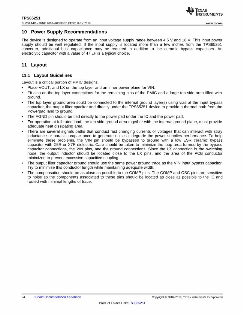
11.1 Layout GuidelinesLayout is a critical portion of PMIC designs.• Place VOUT, and LX on the top layer and an inner power plane for VIN.• Fit also on the top layer connections for the remaining pins of the PMIC and a large top side area filled with
ground.• The top layer ground area sould be connected to the internal ground layer(s) using vias at the input bypass
capacitor, the output filter cpacitor and directly under the TPS65251 device to provide a thermal path from thePowerpad land to ground.
• The AGND pin should be tied directly to the power pad under the IC and the power pad.• For operation at full rated load, the top side ground area together with the internal ground plane, must provide
adequate heat dissipating area.• There are several signals paths that conduct fast changing currents or voltages that can interact with stray
inductance or parasitic capacitance to generate noise or degrade the power supplies performance. To helpeliminate these problems, the VIN pin should be bypassed to ground with a low ESR ceramic bypasscapacitor with X5R or X7R dielectric. Care should be taken to minimize the loop area formed by the bypasscapacitor connections, the VIN pins, and the ground connections. Since the LX connection is the switchingnode, the output inductor should be located close to the LX pins, and the area of the PCB conductorminimized to prevent excessive capacitive coupling.
• The output filter capacitor ground should use the same power ground trace as the VIN input bypass capacitor.Try to minimize this conductor length while maintaining adequate width.
• The compensation should be as close as possible to the COMP pins. The COMP and OSC pins are sensitiveto noise so the components associated to these pins should be located as close as possible to the IC androuted with minimal lengths of trace.
HOT _ SPOT A DIS JAT RT Pq
= + ´
25
TPS65251www.ti.com SLVSAA4G –JUNE 2010–REVISED FEBRUARY 2018
Product Folder Links: TPS65251
Submit Documentation FeedbackCopyright © 2010–2018, Texas Instruments Incorporated
11.2 Layout Example
Figure 35. Layout Schematic
11.3 Power DissipationThe total power dissipation inside TPS65251 should not to exceed the maximum allowable junction temperatureof 125°C. The maximum allowable power dissipation is a function of the thermal resistance of the package (RJA)and ambient temperature.
To calculate the temperature inside the device under continuous loading use the following procedure.1. Define the set voltage for each converter.2. Define the continuous loading on each converter. Make sure do not exceed the converter maximum loading.3. Determine from the graphs below the expected losses (Y axis) in watts per converter inside the device. The
losses depend on the input supply, the selected switching frequency, the output voltage and the converterchosen.
4. To calculate the maximum temperature inside the IC use the following formula:
where• TA is the ambient temperature• PDIS is the sum of losses in all converters• θJA is the junction to ambient thermal impedance of the device and it is heavily dependant on board layout (27)
26
TPS65251SLVSAA4G –JUNE 2010–REVISED FEBRUARY 2018 www.ti.com
Product Folder Links: TPS65251
Submit Documentation Feedback Copyright © 2010–2018, Texas Instruments Incorporated
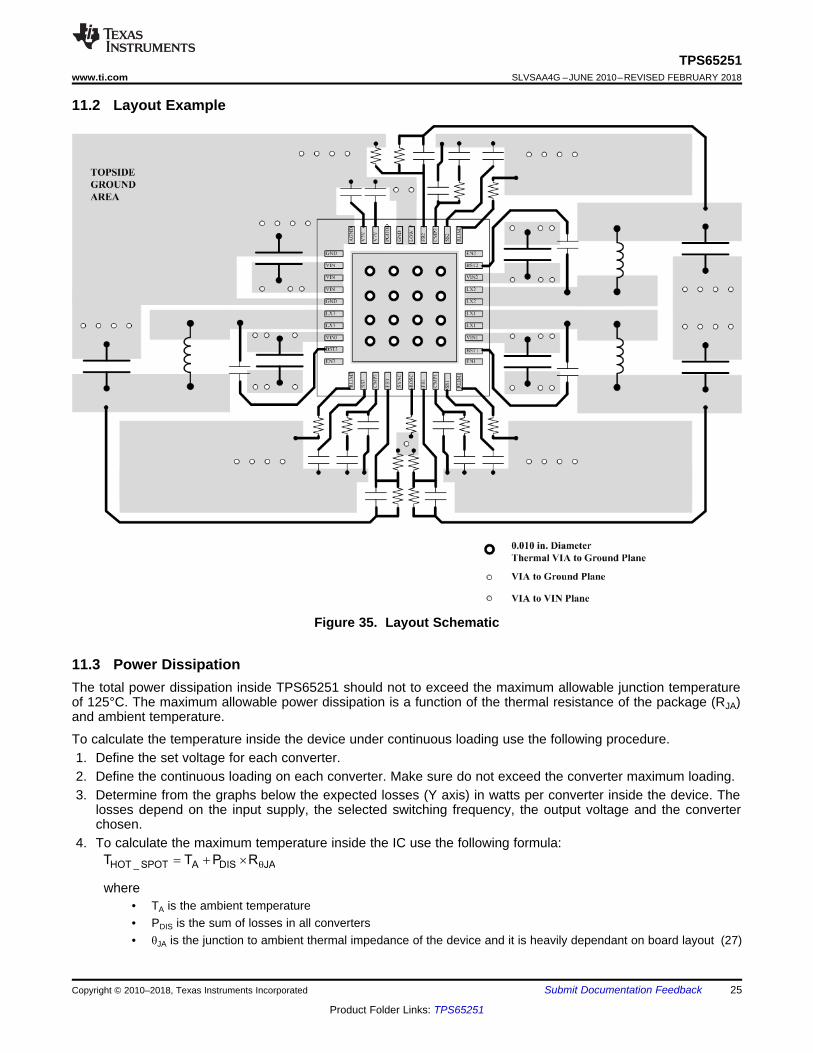
Power Dissipation (continued)
VO (from top to bottom) = 5 V , 3.3 V, 2.5 V, 1.8 V, 1.2 V
Figure 36. Buck 1 Losses (W) vs Output CurrentVIN = 12 V, ƒSW = 500 kHz
VO (from top to bottom) = 5 V , 3.3 V, 2.5 V, 1.8 V, 1.2 V
Figure 37. Buck 1 Losses (W) vs Output CurrentVIN = 12 V, ƒSW = 1.1 MHz
VO (from top to bottom) = 5 V , 3.3 V, 2.5 V, 1.8 V, 1.2 V
Figure 38. Buck 2 and 3 Losses (W) vs Output CurrentVIN = 12 V, ƒSW = 500 kHz
VO (from top to bottom) = 5 V , 3.3 V, 2.5 V, 1.8 V, 1.2 V
Figure 39. Buck 2 and 3 Losses (W) vs Output CurrentVIN = 12 V, ƒSW = 1.1 MHz

27
TPS65251www.ti.com SLVSAA4G –JUNE 2010–REVISED FEBRUARY 2018
Product Folder Links: TPS65251
Submit Documentation FeedbackCopyright © 2010–2018, Texas Instruments Incorporated
12 Device and Documentation Support
12.1 Receiving Notification of Documentation UpdatesTo receive notification of documentation updates, navigate to the device product folder on ti.com. In the upperright corner, click on Alert me to register and receive a weekly digest of any product information that haschanged. For change details, review the revision history included in any revised document.
12.2 Community ResourcesThe following links connect to TI community resources. Linked contents are provided "AS IS" by the respectivecontributors. They do not constitute TI specifications and do not necessarily reflect TI's views; see TI's Terms ofUse.
TI E2E™ Online Community TI's Engineer-to-Engineer (E2E) Community. Created to foster collaborationamong engineers. At e2e.ti.com, you can ask questions, share knowledge, explore ideas and helpsolve problems with fellow engineers.
Design Support TI's Design Support Quickly find helpful E2E forums along with design support tools andcontact information for technical support.
12.3 TrademarksE2E is a trademark of Texas Instruments.All other trademarks are the property of their respective owners.
12.4 Electrostatic Discharge CautionThese devices have limited built-in ESD protection. The leads should be shorted together or the device placed in conductive foamduring storage or handling to prevent electrostatic damage to the MOS gates.
12.5 GlossarySLYZ022 — TI Glossary.
This glossary lists and explains terms, acronyms, and definitions.
13 Mechanical, Packaging, and Orderable InformationThe following pages include mechanical, packaging, and orderable information. This information is the mostcurrent data available for the designated devices. This data is subject to change without notice and revision ofthis document. For browser-based versions of this data sheet, refer to the left-hand navigation.

PACKAGE OPTION ADDENDUM
www.ti.com 1-Feb-2018
Addendum-Page 1
PACKAGING INFORMATION
Orderable Device Status(1)
Package Type PackageDrawing
Pins PackageQty
Eco Plan(2)
Lead/Ball Finish(6)
MSL Peak Temp(3)
Op Temp (°C) Device Marking(4/5)
Samples
905-6525100 ACTIVE VQFN RHA 40 2500 Green (RoHS& no Sb/Br)
CU NIPDAU Level-3-260C-168 HR -40 to 125 TPS65251
TPS65251RHAR ACTIVE VQFN RHA 40 2500 Green (RoHS& no Sb/Br)
CU NIPDAU Level-3-260C-168 HR -40 to 125 TPS65251
TPS65251RHAT ACTIVE VQFN RHA 40 250 Green (RoHS& no Sb/Br)
CU NIPDAU Level-3-260C-168 HR -40 to 125 TPS65251
(1) The marketing status values are defined as follows:ACTIVE: Product device recommended for new designs.LIFEBUY: TI has announced that the device will be discontinued, and a lifetime-buy period is in effect.NRND: Not recommended for new designs. Device is in production to support existing customers, but TI does not recommend using this part in a new design.PREVIEW: Device has been announced but is not in production. Samples may or may not be available.OBSOLETE: TI has discontinued the production of the device.
(2) RoHS: TI defines "RoHS" to mean semiconductor products that are compliant with the current EU RoHS requirements for all 10 RoHS substances, including the requirement that RoHS substancedo not exceed 0.1% by weight in homogeneous materials. Where designed to be soldered at high temperatures, "RoHS" products are suitable for use in specified lead-free processes. TI mayreference these types of products as "Pb-Free".RoHS Exempt: TI defines "RoHS Exempt" to mean products that contain lead but are compliant with EU RoHS pursuant to a specific EU RoHS exemption.Green: TI defines "Green" to mean the content of Chlorine (Cl) and Bromine (Br) based flame retardants meet JS709B low halogen requirements of <=1000ppm threshold. Antimony trioxide basedflame retardants must also meet the <=1000ppm threshold requirement.
(3) MSL, Peak Temp. - The Moisture Sensitivity Level rating according to the JEDEC industry standard classifications, and peak solder temperature.
(4) There may be additional marking, which relates to the logo, the lot trace code information, or the environmental category on the device.
(5) Multiple Device Markings will be inside parentheses. Only one Device Marking contained in parentheses and separated by a "~" will appear on a device. If a line is indented then it is a continuationof the previous line and the two combined represent the entire Device Marking for that device.
(6) Lead/Ball Finish - Orderable Devices may have multiple material finish options. Finish options are separated by a vertical ruled line. Lead/Ball Finish values may wrap to two lines if the finishvalue exceeds the maximum column width.
Important Information and Disclaimer:The information provided on this page represents TI's knowledge and belief as of the date that it is provided. TI bases its knowledge and belief on informationprovided by third parties, and makes no representation or warranty as to the accuracy of such information. Efforts are underway to better integrate information from third parties. TI has taken andcontinues to take reasonable steps to provide representative and accurate information but may not have conducted destructive testing or chemical analysis on incoming materials and chemicals.TI and TI suppliers consider certain information to be proprietary, and thus CAS numbers and other limited information may not be available for release.

PACKAGE OPTION ADDENDUM
www.ti.com 1-Feb-2018
Addendum-Page 2
In no event shall TI's liability arising out of such information exceed the total purchase price of the TI part(s) at issue in this document sold by TI to Customer on an annual basis.
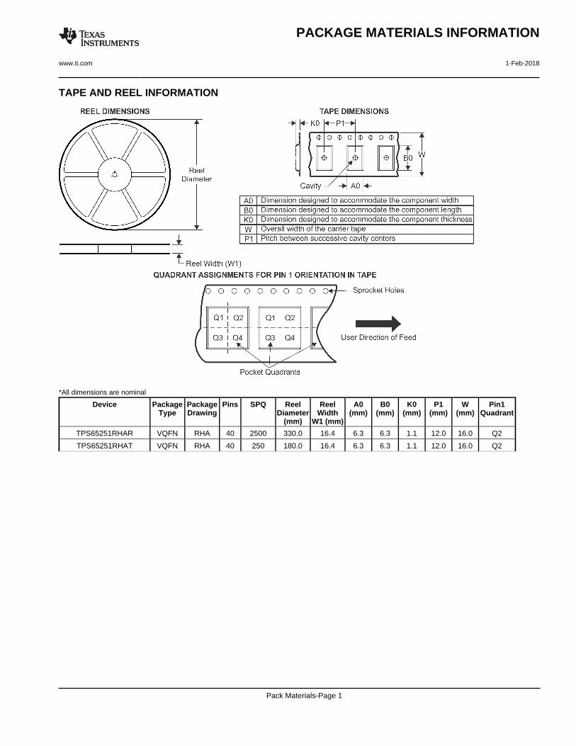
TAPE AND REEL INFORMATION
*All dimensions are nominal
Device PackageType
PackageDrawing
Pins SPQ ReelDiameter
(mm)
ReelWidth
W1 (mm)
A0(mm)
B0(mm)
K0(mm)
P1(mm)
W(mm)
Pin1Quadrant
TPS65251RHAR VQFN RHA 40 2500 330.0 16.4 6.3 6.3 1.1 12.0 16.0 Q2
TPS65251RHAT VQFN RHA 40 250 180.0 16.4 6.3 6.3 1.1 12.0 16.0 Q2
PACKAGE MATERIALS INFORMATION
www.ti.com 1-Feb-2018
Pack Materials-Page 1

*All dimensions are nominal
Device Package Type Package Drawing Pins SPQ Length (mm) Width (mm) Height (mm)
TPS65251RHAR VQFN RHA 40 2500 367.0 367.0 38.0
TPS65251RHAT VQFN RHA 40 250 210.0 185.0 35.0
PACKAGE MATERIALS INFORMATION
www.ti.com 1-Feb-2018
Pack Materials-Page 2


IMPORTANT NOTICE
Texas Instruments Incorporated (TI) reserves the right to make corrections, enhancements, improvements and other changes to itssemiconductor products and services per JESD46, latest issue, and to discontinue any product or service per JESD48, latest issue. Buyersshould obtain the latest relevant information before placing orders and should verify that such information is current and complete.TI’s published terms of sale for semiconductor products (http://www.ti.com/sc/docs/stdterms.htm) apply to the sale of packaged integratedcircuit products that TI has qualified and released to market. Additional terms may apply to the use or sale of other types of TI products andservices.Reproduction of significant portions of TI information in TI data sheets is permissible only if reproduction is without alteration and isaccompanied by all associated warranties, conditions, limitations, and notices. TI is not responsible or liable for such reproduceddocumentation. Information of third parties may be subject to additional restrictions. Resale of TI products or services with statementsdifferent from or beyond the parameters stated by TI for that product or service voids all express and any implied warranties for theassociated TI product or service and is an unfair and deceptive business practice. TI is not responsible or liable for any such statements.Buyers and others who are developing systems that incorporate TI products (collectively, “Designers”) understand and agree that Designersremain responsible for using their independent analysis, evaluation and judgment in designing their applications and that Designers havefull and exclusive responsibility to assure the safety of Designers' applications and compliance of their applications (and of all TI productsused in or for Designers’ applications) with all applicable regulations, laws and other applicable requirements. Designer represents that, withrespect to their applications, Designer has all the necessary expertise to create and implement safeguards that (1) anticipate dangerousconsequences of failures, (2) monitor failures and their consequences, and (3) lessen the likelihood of failures that might cause harm andtake appropriate actions. Designer agrees that prior to using or distributing any applications that include TI products, Designer willthoroughly test such applications and the functionality of such TI products as used in such applications.TI’s provision of technical, application or other design advice, quality characterization, reliability data or other services or information,including, but not limited to, reference designs and materials relating to evaluation modules, (collectively, “TI Resources”) are intended toassist designers who are developing applications that incorporate TI products; by downloading, accessing or using TI Resources in anyway, Designer (individually or, if Designer is acting on behalf of a company, Designer’s company) agrees to use any particular TI Resourcesolely for this purpose and subject to the terms of this Notice.TI’s provision of TI Resources does not expand or otherwise alter TI’s applicable published warranties or warranty disclaimers for TIproducts, and no additional obligations or liabilities arise from TI providing such TI Resources. TI reserves the right to make corrections,enhancements, improvements and other changes to its TI Resources. TI has not conducted any testing other than that specificallydescribed in the published documentation for a particular TI Resource.Designer is authorized to use, copy and modify any individual TI Resource only in connection with the development of applications thatinclude the TI product(s) identified in such TI Resource. NO OTHER LICENSE, EXPRESS OR IMPLIED, BY ESTOPPEL OR OTHERWISETO ANY OTHER TI INTELLECTUAL PROPERTY RIGHT, AND NO LICENSE TO ANY TECHNOLOGY OR INTELLECTUAL PROPERTYRIGHT OF TI OR ANY THIRD PARTY IS GRANTED HEREIN, including but not limited to any patent right, copyright, mask work right, orother intellectual property right relating to any combination, machine, or process in which TI products or services are used. Informationregarding or referencing third-party products or services does not constitute a license to use such products or services, or a warranty orendorsement thereof. Use of TI Resources may require a license from a third party under the patents or other intellectual property of thethird party, or a license from TI under the patents or other intellectual property of TI.TI RESOURCES ARE PROVIDED “AS IS” AND WITH ALL FAULTS. TI DISCLAIMS ALL OTHER WARRANTIES ORREPRESENTATIONS, EXPRESS OR IMPLIED, REGARDING RESOURCES OR USE THEREOF, INCLUDING BUT NOT LIMITED TOACCURACY OR COMPLETENESS, TITLE, ANY EPIDEMIC FAILURE WARRANTY AND ANY IMPLIED WARRANTIES OFMERCHANTABILITY, FITNESS FOR A PARTICULAR PURPOSE, AND NON-INFRINGEMENT OF ANY THIRD PARTY INTELLECTUALPROPERTY RIGHTS. TI SHALL NOT BE LIABLE FOR AND SHALL NOT DEFEND OR INDEMNIFY DESIGNER AGAINST ANY CLAIM,INCLUDING BUT NOT LIMITED TO ANY INFRINGEMENT CLAIM THAT RELATES TO OR IS BASED ON ANY COMBINATION OFPRODUCTS EVEN IF DESCRIBED IN TI RESOURCES OR OTHERWISE. IN NO EVENT SHALL TI BE LIABLE FOR ANY ACTUAL,DIRECT, SPECIAL, COLLATERAL, INDIRECT, PUNITIVE, INCIDENTAL, CONSEQUENTIAL OR EXEMPLARY DAMAGES INCONNECTION WITH OR ARISING OUT OF TI RESOURCES OR USE THEREOF, AND REGARDLESS OF WHETHER TI HAS BEENADVISED OF THE POSSIBILITY OF SUCH DAMAGES.Unless TI has explicitly designated an individual product as meeting the requirements of a particular industry standard (e.g., ISO/TS 16949and ISO 26262), TI is not responsible for any failure to meet such industry standard requirements.Where TI specifically promotes products as facilitating functional safety or as compliant with industry functional safety standards, suchproducts are intended to help enable customers to design and create their own applications that meet applicable functional safety standardsand requirements. Using products in an application does not by itself establish any safety features in the application. Designers mustensure compliance with safety-related requirements and standards applicable to their applications. Designer may not use any TI products inlife-critical medical equipment unless authorized officers of the parties have executed a special contract specifically governing such use.Life-critical medical equipment is medical equipment where failure of such equipment would cause serious bodily injury or death (e.g., lifesupport, pacemakers, defibrillators, heart pumps, neurostimulators, and implantables). Such equipment includes, without limitation, allmedical devices identified by the U.S. Food and Drug Administration as Class III devices and equivalent classifications outside the U.S.TI may expressly designate certain products as completing a particular qualification (e.g., Q100, Military Grade, or Enhanced Product).Designers agree that it has the necessary expertise to select the product with the appropriate qualification designation for their applicationsand that proper product selection is at Designers’ own risk. Designers are solely responsible for compliance with all legal and regulatoryrequirements in connection with such selection.Designer will fully indemnify TI and its representatives against any damages, costs, losses, and/or liabilities arising out of Designer’s non-compliance with the terms and provisions of this Notice.
Mailing Address: Texas Instruments, Post Office Box 655303, Dallas, Texas 75265Copyright © 2018, Texas Instruments Incorporated