ads8320 16-bit, high-speed, 2.7-v to 5-v micropower ... · package type package drawing pins...
TRANSCRIPT

SAR Control
SerialInterface
DOUT
ComparatorS/H AmpCS/SHDN
DCLOCK
+In
VREF
±InCDAC
Copyright © 2016, Texas Instruments Incorporated
Product
Folder
Sample &Buy
Technical
Documents
Tools &
Software
Support &Community
ReferenceDesign
An IMPORTANT NOTICE at the end of this data sheet addresses availability, warranty, changes, use in safety-critical applications,intellectual property matters and other important disclaimers. PRODUCTION DATA.
ADS8320SBAS108E –MAY 2000–REVISED DECEMBER 2016
ADS8320 16-Bit, High-Speed, 2.7-V to 5-V microPower SamplingAnalog-to-Digital Converter
1
1 Features1• 100-kHz Sampling Rate• microPower:
– 1.8 mW at 100 kHz and 2.7 V– 0.3 mW at 10 kHz and 2.7 V
• Power Down: 3 µA (Maximum)• 8-Pin VSSOP Package• Pin-Compatible to ADS7816 and ADS7822• Serial (SPI™/SSI) Interface
2 Applications• Battery-Operated Systems• Remote Data Acquisition• Isolated Data Acquisition• Simultaneous Sampling, Multichannel Systems• Industrial Controls• Robotics• Vibration Analysis
3 DescriptionThe ADS8320 device is a 16-bit, sampling analog-to-digital (A/D) converter with ensured specificationsover a 2.7-V to 5.25-V supply range. It requires verylittle power even when operating at the full 100-kHzdata rate. At lower data rates, the high speed of thedevice enables it to spend most of its time in thepower-down mode. The average power dissipation isless than 100 mW at 10-kHz data rate.
The ADS8320 also features operation from 2 V to5.25 V, a synchronous serial (SPI/SSI compatible)interface, and a differential input. The referencevoltage can be set to any level within the range of500 mV to VCC.
Ultra-low power and small size make the ADS8320ideal for portable and battery-operated systems. It isalso a perfect fit for remote data acquisition modules,simultaneous multi-channel systems, and isolateddata acquisition. The ADS8320 is available in an8-pin VSSOP package.
Device Information(1)
PART NUMBER PACKAGE BODY SIZE (NOM)ADS8320 VSSOP (8) 3.00 mm × 3.00 mm
(1) For all available packages, see the orderable addendum atthe end of the data sheet.
Block Diagram

2
ADS8320SBAS108E –MAY 2000–REVISED DECEMBER 2016 www.ti.com
Product Folder Links: ADS8320
Submit Documentation Feedback Copyright © 2000–2016, Texas Instruments Incorporated
Table of Contents1 Features .................................................................. 12 Applications ........................................................... 13 Description ............................................................. 14 Revision History..................................................... 25 Pin Configuration and Functions ......................... 36 Specifications......................................................... 4
6.1 Absolute Maximum Ratings ...................................... 46.2 ESD Ratings.............................................................. 46.3 Recommended Operating Conditions....................... 46.4 Thermal Information .................................................. 46.5 Electrical Characteristics: VCC = 5 V......................... 56.6 Electrical Characteristics: VCC = 2.7 V...................... 66.7 Typical Characteristics .............................................. 8
7 Detailed Description ............................................ 117.1 Overview ................................................................. 117.2 Functional Block Diagram ....................................... 127.3 Feature Description................................................. 12
7.4 Device Functional Modes........................................ 138 Application and Implementation ........................ 16
8.1 Application Information............................................ 168.2 Typical Applications ................................................ 16
9 Power Supply Recommendations ...................... 2210 Layout................................................................... 22
10.1 Layout Guidelines ................................................. 2210.2 Layout Example .................................................... 2310.3 Power Dissipation ................................................. 23
11 Device and Documentation Support ................. 2711.1 Documentation Support ........................................ 2711.2 Receiving Notification of Documentation Updates 2711.3 Community Resources.......................................... 2711.4 Trademarks ........................................................... 2711.5 Electrostatic Discharge Caution............................ 2711.6 Glossary ................................................................ 27
12 Mechanical, Packaging, and OrderableInformation ........................................................... 27
4 Revision History
Changes from Revision D (March 2007) to Revision E Page
• Added ESD Ratings table, Feature Description section, Device Functional Modes, Application and Implementationsection, Power Supply Recommendations section, Layout section, Device and Documentation Support section, andMechanical, Packaging, and Orderable Information section ................................................................................................. 1
• Added Thermal Information table ........................................................................................................................................... 4• Changed Application Circuits section To: Typical Connection Diagram .............................................................................. 11
1
2
3
4
8
7
6
5
+VCC
DCLOCK
DOUT
CS/SHDN
VREF
+In
±In
GND
ADS8320
3
ADS8320www.ti.com SBAS108E –MAY 2000–REVISED DECEMBER 2016
Product Folder Links: ADS8320
Submit Documentation FeedbackCopyright © 2000–2016, Texas Instruments Incorporated
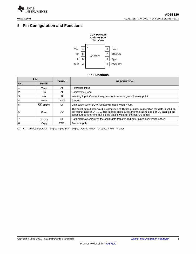
(1) AI = Analog Input, DI = Digital Input, DO = Digital Output, GND = Ground, PWR = Power
5 Pin Configuration and Functions
DGK Package8-Pin VSSOP
Top View
Pin FunctionsPIN
TYPE (1) DESCRIPTIONNO. NAME1 VREF AI Reference input2 +In AI Noninverting input3 –In AI Inverting input: Connect to ground or to remote ground sense point.4 GND GND Ground5 CS/SHDN DI Chip select when LOW; Shutdown mode when HIGH.
6 DOUT DOThe serial output data word is comprised of 16 bits of data. In operation the data is valid onthe falling edge of DCLOCK. The second clock pulse after the falling edge of CS enables theserial output. After one null bit the data is valid for the next 16 edges.
7 DCLOCK DI Data clock synchronizes the serial data transfer and determines conversion speed.8 +VCC PWR Power supply

4
ADS8320SBAS108E –MAY 2000–REVISED DECEMBER 2016 www.ti.com
Product Folder Links: ADS8320
Submit Documentation Feedback Copyright © 2000–2016, Texas Instruments Incorporated
(1) Stresses beyond those listed under Absolute Maximum Ratings may cause permanent damage to the device. These are stress ratingsonly, which do not imply functional operation of the device at these or any other conditions beyond those indicated under RecommendedOperating Conditions. Exposure to absolute-maximum-rated conditions for extended periods may affect device reliability.
6 Specifications
6.1 Absolute Maximum Ratingsover operating free-air temperature range (unless otherwise noted) (1)
MIN MAX UNITVCC 6 VAnalog input –0.3 VCC + 0.3 VLogic input –0.3 6 °CExternal reference voltage 5.5 VInput current to any pin except supply ±10 mACase temperature 100 °CJunction temperature 150 °CStorage temperature, Tstg 125 °C
(1) JEDEC document JEP155 states that 500-V HBM allows safe manufacturing with a standard ESD control process.(2) JEDEC document JEP157 states that 250-V CDM allows safe manufacturing with a standard ESD control process.
6.2 ESD RatingsVALUE UNIT
V(ESD)Electrostaticdischarge
Human-body model (HBM), per ANSI/ESDA/JEDEC JS-001 (1) ±2000V
Charged-device model (CDM), per JEDEC specification JESD22-C101 (2) ±1000
6.3 Recommended Operating Conditionsover operating free-air temperature range (unless otherwise noted)
MIN NOM MAX UNIT
Supply voltage, VCC to GNDLow voltage levels 2.7 3.3
V5-V logic levels 4.75 5 5.25
Reference input voltage, VREF 0.5 VCC V
Analog input voltage–IN to GND –0.1 0 0.5
V+IN to GND –0.1 VCC + 0.1+IN to – (–IN) 0 VREF
Operating temperature, TA –40 85 °C
(1) For more information about traditional and new thermal metrics, see the Semiconductor and IC Package Thermal Metrics applicationreport.
6.4 Thermal Information
THERMAL METRIC (1)ADS8320
UNITDGK (VSSOP)8 PINS
RθJA Junction-to-ambient thermal resistance 163.1 °C/WRθJC(top) Junction-to-case (top) thermal resistance 56.6 °C/WRθJB Junction-to-board thermal resistance 83.4 °C/WψJT Junction-to-top characterization parameter 6.7 °C/WψJB Junction-to-board characterization parameter 82 °C/WRθJC(bot) Junction-to-case (bottom) thermal resistance — °C/W

5
ADS8320www.ti.com SBAS108E –MAY 2000–REVISED DECEMBER 2016
Product Folder Links: ADS8320
Submit Documentation FeedbackCopyright © 2000–2016, Texas Instruments Incorporated
(1) LSB means Least Significant Bit with VREF equal to 2.5 V, one LSB is 0.038 mV.
6.5 Electrical Characteristics: VCC = 5 Vat –40°C to 85°C, VREF = 5 V, –IN = GND, fSAMPLE = 100 kHz, and fCLK = 24 × fSAMPLE (unless otherwise noted)
PARAMETER TEST CONDITIONS MIN TYP MAX UNITRESOLUTIONResolution 16 BitsANALOG INPUTFull-scale input span +In – (–In) 0 VREF V
Absolute input+In –0.1 VCC + 0.1
V–In –0.1 1
Capacitance 45 pFLeakage current 1 nASYSTEM PERFORMANCE
No missing codesADS8320E 14
BitsADS8320EB 15
Integral linearity errorADS8320E ±0.008% ±0.018%
FSRADS8320EB ±0.006% ±0.012%
Offset errorADS8320E ±1 ±2
mVADS8320EB ±0.5 ±1
Offset temperature drift ±3 µV/°C
Gain errorADS8320E ±0.05%
FSRADS8320EB ±0.024%
Gain error temperature drift ±0.3 ppm/°CNoise 20 µVrmsPower-supply rejection ratio 4.7 V < VCC < 5.25 V 3 LSB (1)
SAMPLING DYNAMICS
Conversion time 16 ClockCycles
Acquisition time 4.5 ClockCycles
Throughput rate 100 kHzClock frequency 0.024 2.4 MHzDYNAMIC CHARACTERISTICS
Total harmonic distortion VIN = 5 VP-P at 10 kHzADS8320E –84
dBADS8320EB –86
SINAD VIN = 5 VP-P at 10 kHzADS8320E 82
dBADS8320EB 84
Spurious-free dynamic VIN = 5 VP-P at 10 kHzADS8320E 84
dBADS8320EB 86
SNRADS8320E 90
dBADS8320EB 92
REFERENCE INPUTVoltage 0.5 VCC V
ResistanceCS = GND, fSAMPLE = 0 Hz 5
GΩCS = VCC 5
Current drain40 80
µAfSAMPLE = 0 Hz 0.8CS = VCC 0.1 3

6
ADS8320SBAS108E –MAY 2000–REVISED DECEMBER 2016 www.ti.com
Product Folder Links: ADS8320
Submit Documentation Feedback Copyright © 2000–2016, Texas Instruments Incorporated
Electrical Characteristics: VCC = 5 V (continued)at –40°C to 85°C, VREF = 5 V, –IN = GND, fSAMPLE = 100 kHz, and fCLK = 24 × fSAMPLE (unless otherwise noted)
PARAMETER TEST CONDITIONS MIN TYP MAX UNIT
(2) See Typical Characteristics for more information.(3) fCLK = 2.4 MHz, CS = VCC for 216 clock cycles out of every 240.(4) See Power Dissipation for more information regarding lower sample rates.
DIGITAL INPUT/OUTPUTLogic family CMOS
Logic levels
VIH IIH = 5 µA 3 VCC + 0.3
VVIL IIL = 5 µA –0.3 0.8VOH IOH = –250 µA 4VOL IOL = 250 µA 0.4
Data format Straight BinaryPOWER SUPPLY REQUIREMENTSVCC Specified performance 4.75 5.25 VVCC
(2) 2 5.25 V
Quiescent current900 1700
µAfSAMPLE = 10 kHz (3) (4) 200
Power dissipation 4.5 8.5 mWPower down CS = VCC 0.3 3 µA
(1) LSB means Least Significant Bit with VREF equal to 2.5 V, one LSB is 0.038 mV.
6.6 Electrical Characteristics: VCC = 2.7 Vat –40°C to 85°C, VREF = 5 V, –IN = GND, fSAMPLE = 100 kHz, and fCLK = 24 × fSAMPLE (unless otherwise noted)
PARAMETER TEST CONDITIONS MIN TYP MAX UNITRESOLUTIONResolution 16 BitsANALOG INPUTFull-scale input span +In – (–In) 0 VREF V
Absolute input+In –0.1 VCC + 0.1
V–In –0.1 0.5
Capacitance 45 pFLeakage current 1 nASYSTEM PERFORMANCE
No missing codesADS8320E 14
BitsADS8320EB 15
Integral linearity errorADS8320E ±0.008% ±0.018%
FSRADS8320EB ±0.006% ±0.012%
Offset errorADS8320E ±1 ±2
mVADS8320EB ±0.5 ±1
Offset temperature drift ±3 µV/°C
Gain errorADS8320E ±0.05%
FSRADS8320EB ±0.024%
Gain error temperature drift ±0.3 ppm/°CNoise 20 ppm/°CPower-supply rejection ratio 2.7 V < VCC < 3.3 V 3 LSB (1)

7
ADS8320www.ti.com SBAS108E –MAY 2000–REVISED DECEMBER 2016
Product Folder Links: ADS8320
Submit Documentation FeedbackCopyright © 2000–2016, Texas Instruments Incorporated
Electrical Characteristics: VCC = 2.7 V (continued)at –40°C to 85°C, VREF = 5 V, –IN = GND, fSAMPLE = 100 kHz, and fCLK = 24 × fSAMPLE (unless otherwise noted)
PARAMETER TEST CONDITIONS MIN TYP MAX UNIT
(2) See Typical Characteristics for more information.(3) The maximum clock rate of the ADS8320 is less than 2.4 MHz in this power supply range.(4) fCLK = 2.4 MHz, CS = VCC for 216 clock cycles out of every 240.(5) See Power Dissipation for more information regarding lower sample rates.
SAMPLING DYNAMICS
Conversion time 16 ClockCycles
Acquisition time 4.5 ClockCycles
Throughput rate 100 kHzClock frequency 0.024 2.4 MHzDYNAMIC CHARACTERISTICS
Total harmonic distortion VIN = 2.7 VP-P at 1 kHzADS8320E –86
dBADS8320EB –88
SINAD VIN = 2.7 VP-P at 1 kHzADS8320E 84
dBADS8320EB 86
Spurious-free dynamic VIN = 2.7 VP-P at 1 kHzADS8320E 86
dBADS8320EB 88
SNRADS8320E 88
dBADS8320EB 90
REFERENCE INPUTVoltage 0.5 VCC V
ResistanceCS = GND, fSAMPLE = 0 Hz 5
GΩCS = VCC 5
Current drain20 50
µACS = VCC 0.1 3
DIGITAL INPUT/OUTPUTLogic Family CMOS
Logic levels
VIH IIH = 5 µA 2 VCC + 0.3
VVIL IIL = 5 µA –0.3 0.8VOH IOH = –250 µA 2.1VOL IOL = 250 µA 0.4
Data format Straight BinaryPOWER SUPPLY REQUIREMENTSVCC Specified performance 2.7 3.3 V
VCC(2) 2 5.25
VSee (3) 2 2.7
Quiescent current650 1300
µAfSAMPLE = 10 kHz (4) (5) 100
Power dissipation 1.8 3.8 mWPower down CS = VCC 0.3 3 µA

1200
1000
800
600
400
200
Qui
esce
nt C
urre
nt (
µA
)
1 2 3 4 5
VCC (V)
1000
100
10
1
Sam
ple
Rat
e (k
Hz)
1 2 3 4 5
VCC (V)
1200
1000
800
600
400
200
0
Sup
ply
Cur
rent
(µ
A)
±50 ±25 0 25 50 75 100
Temperature (°C)
2.7V
5V
600
500
400
300
200
100
0
Sup
ply
Cur
rent
(nA
)
±50 ±25 0 25 50 75 100
Temperature (°C)
5V
2.0
1.0
0.0
±1.0
±2.0
±3.0
±4.0
±5.0
±6.0
Inte
gral
Non
Lin
earit
y (L
SB
)
0000H 8000H C000H4000H FFFFH
Hex Code
3.0
2.0
1.0
0.0
±1.0
±2.0
±3.00000H 8000H C000H4000H FFFFH
Hex Code
Non
Lin
earit
y (L
SB
)
8
ADS8320SBAS108E –MAY 2000–REVISED DECEMBER 2016 www.ti.com
Product Folder Links: ADS8320
Submit Documentation Feedback Copyright © 2000–2016, Texas Instruments Incorporated
6.7 Typical Characteristics
Figure 1. Integral Non-Linearity (INL) vs Code (25°C) Figure 2. Differential Non-Linearity Error vs Code (25°C)
Figure 3. Supply Current vs Temperature Figure 4. Power-Down Supply CurrentCode (25°C)
Figure 5. Quiescent Current vs VCC Figure 6. Maximum Sample Rate vs VCC

0
±20
±40
±60
±80
±100
±120
±140
Am
plitu
de (
dB)
0 10 20 30 40 50
Frequency (kHz)
10
9
8
7
6
5
4
3
2
1
0
Pea
k-to
-Pea
k N
oise
(LS
B)
0.1 1 10
Reference Voltage (V)
VCC = 5V
5
4
3
2
1
0
±1
±2
Cha
nge
in G
ain
(LS
B)
1 2 3 4 5Reference Voltage (V)
VCC = 5V6
4
2
0
±2
±4
±6
Del
ta fr
om 2
5°C
(LS
B)
±50 ±25 0 25 50 75 100
Temperature (°C)
5V
2.7V
6
5
4
3
2
1
0
±1
±2
±3
Cha
nge
in O
ffset
(LS
B)
1 2 3 4 5Reference Voltage (V)
VCC = 5V3
2
1
0
í1
í2
í3
Del
ta fr
om +
25C
(LS
B)
í50 í25 0 25 50 75 100
Temperature (°C)
5V
2.7V
9
ADS8320www.ti.com SBAS108E –MAY 2000–REVISED DECEMBER 2016
Product Folder Links: ADS8320
Submit Documentation FeedbackCopyright © 2000–2016, Texas Instruments Incorporated
Typical Characteristics (continued)
Figure 7. Change In Offset vs Reference Voltage Figure 8. Change In Offset vs Temperature
Figure 9. Change In Gain Error vs Reference Voltage Figure 10. Change In Gain Error vs Temperature
Figure 11. Frequency Spectrum (8192 Point FFT,FIN = 10.120 kHz, –0.3 dB)
Figure 12. Peak-to-Peak Noise vs Reference Voltage

70
60
50
40
30
20
10
Ref
eren
ce C
urre
nt (
µA
)
±50 ±25 0 25 50 75 100
Temperature (°C)
5V
2.7V
70
60
50
40
30
20
10
0
Ref
eren
ce C
urre
nt (
µA
)
0 20 40 60 80 100Sample Rate (kHz)
5V
2.7V
100
90
80
70
60
50
40
30
20
10
0
Sig
nal-t
o-(N
oise
+ D
isto
rtio
n)
(dB
)
1 10 50 100
Frequency (kHz)
90
80
70
60
50
40
30
20
Sig
nal-t
o-(N
oise
+ D
isto
rtio
n) (
dB)
±40 ±35 ±30 ±25 ±20 ±15 ±10 ±5 0Input Level (dB)
100
90
80
70
60
50
40
30
20
10
0
Spu
rious
-Fre
e D
ynam
ic R
ange
and
Sig
nal-t
o-N
oise
Rat
io (
dB)
1 10 10050
Frequency (kHz)
Signal-to-Noise Ratio
Spurious-Free Dynamic Range
0
±10
±20
±30
±40
±50
±60
±70
±80
±90
±100
Tota
l Har
mon
ic D
isto
rtio
n (d
B)
1 10 100
Frequency (kHz)
10
ADS8320SBAS108E –MAY 2000–REVISED DECEMBER 2016 www.ti.com
Product Folder Links: ADS8320
Submit Documentation Feedback Copyright © 2000–2016, Texas Instruments Incorporated
Typical Characteristics (continued)
Figure 13. Spurious-Free Dynamic Range and Signal-to-Noise Ratio vs Frequency
Figure 14. Total Harmonic Distortion vs Frequency
Figure 15. Signal-to-(Noise + Distortion) vs Frequency Figure 16. Signal-to-(Noise + Distortion) vs Input Level
Figure 17. Reference Current vs Sample Rate Figure 18. Reference Current vs Temperature
ADS8320
VCC
DOUT
DCLOCK
VREF
+In
±In
GND
+
+
5 �
1 µF to10 µF
1 µF to10 µF
0.1µF
Microcontroller
+2.7 V to +5.25 V
CS
Copyright © 2016, Texas Instruments Incorporated
11
ADS8320www.ti.com SBAS108E –MAY 2000–REVISED DECEMBER 2016
Product Folder Links: ADS8320
Submit Documentation FeedbackCopyright © 2000–2016, Texas Instruments Incorporated
7 Detailed Description
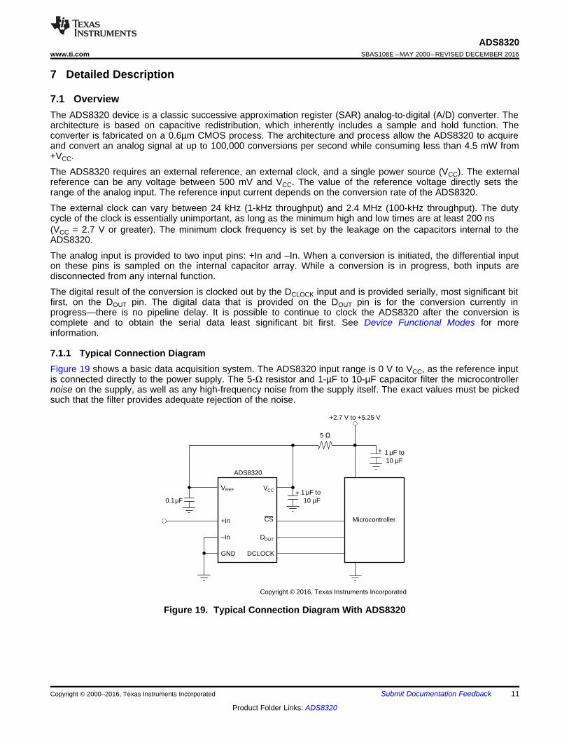
7.1 OverviewThe ADS8320 device is a classic successive approximation register (SAR) analog-to-digital (A/D) converter. Thearchitecture is based on capacitive redistribution, which inherently includes a sample and hold function. Theconverter is fabricated on a 0.6µm CMOS process. The architecture and process allow the ADS8320 to acquireand convert an analog signal at up to 100,000 conversions per second while consuming less than 4.5 mW from+VCC.
The ADS8320 requires an external reference, an external clock, and a single power source (VCC). The externalreference can be any voltage between 500 mV and VCC. The value of the reference voltage directly sets therange of the analog input. The reference input current depends on the conversion rate of the ADS8320.
The external clock can vary between 24 kHz (1-kHz throughput) and 2.4 MHz (100-kHz throughput). The dutycycle of the clock is essentially unimportant, as long as the minimum high and low times are at least 200 ns(VCC = 2.7 V or greater). The minimum clock frequency is set by the leakage on the capacitors internal to theADS8320.
The analog input is provided to two input pins: +In and –In. When a conversion is initiated, the differential inputon these pins is sampled on the internal capacitor array. While a conversion is in progress, both inputs aredisconnected from any internal function.
The digital result of the conversion is clocked out by the DCLOCK input and is provided serially, most significant bitfirst, on the DOUT pin. The digital data that is provided on the DOUT pin is for the conversion currently inprogress—there is no pipeline delay. It is possible to continue to clock the ADS8320 after the conversion iscomplete and to obtain the serial data least significant bit first. See Device Functional Modes for moreinformation.
7.1.1 Typical Connection DiagramFigure 19 shows a basic data acquisition system. The ADS8320 input range is 0 V to VCC, as the reference inputis connected directly to the power supply. The 5-Ω resistor and 1-µF to 10-µF capacitor filter the microcontrollernoise on the supply, as well as any high-frequency noise from the supply itself. The exact values must be pickedsuch that the filter provides adequate rejection of the noise.
Figure 19. Typical Connection Diagram With ADS8320

SAR Control
SerialInterface
DOUT
ComparatorS/H AmpCS/SHDN
DCLOCK
+In
VREF
±InCDAC
Copyright © 2016, Texas Instruments Incorporated
12
ADS8320SBAS108E –MAY 2000–REVISED DECEMBER 2016 www.ti.com
Product Folder Links: ADS8320
Submit Documentation Feedback Copyright © 2000–2016, Texas Instruments Incorporated
7.2 Functional Block Diagram
7.3 Feature Description
7.3.1 Analog InputThe +In and –In input pins allow for a differential input signal. Unlike some converters of this type, the –In input isnot resampled later in the conversion cycle. When the converter goes into the hold mode, the voltage differencebetween +In and –In is captured on the internal capacitor array.
The range of the –In input is limited to –0.1 V to 1 V (–0.1 V to 0.5 V when using a 2.7-V supply). Because ofthis, the differential input can be used to reject only small signals that are common to both inputs. Thus, the –Ininput is best used to sense a remote signal ground that may move slightly with respect to the local groundpotential.
The input current on the analog inputs depends on a number of factors: sample rate, input voltage, sourceimpedance, and power-down mode. Essentially, the current into the ADS8320 charges the internal capacitorarray during the sample period. After this capacitance has been fully charged, there is no further input current.The source of the analog input voltage must be able to charge the input capacitance (45 pF) to a 16-bit settlinglevel within 4.5 clock cycles. When the converter goes into the hold mode or while it is in the power down mode,the input impedance is greater than 1 GΩ.
Care must be taken regarding the absolute analog input voltage. To maintain the linearity of the converter, the–In input must not drop below GND – 100 mV or exceed GND + 1 V. The +In input must always remain withinthe range of GND – 100 mV to VCC + 100 mV. Outside of these ranges, the converter linearity may not meetspecifications. To minimize noise, low bandwidth input signals with lowpass filters must be used.
7.3.2 Reference InputThe external reference sets the analog input range. The ADS8320 operates with a reference in the range of 500mV to VCC. There are several important implications of this.
As the reference voltage is reduced, the analog voltage weight of each digital output code is reduced. This isoften referred to as the Least Significant Bit (LSB) size and is equal to the reference voltage divided by 65,536.This means that any offset or gain error inherent in the A/D converter appears to increase, in terms of LSB size,as the reference voltage is reduced.
The noise inherent in the converter also appears to increase with lower LSB size. With a 5-V reference, theinternal noise of the converter typically contributes only 1.5-LSB peak-to-peak of potential error to the outputcode. When the external reference is 500 mV, the potential error contribution from the internal noise is 10 timeslarger (15 LSBs). The errors due to the internal noise are gaussian in nature and can be reduced by averagingconsecutive conversion results.
For more information regarding noise, see Figure 12. Note that the Effective Number of Bits (ENOB) figure iscalculated based on the converter’s signal-to-(noise + distortion) ratio with a 1-kHz, 0-dB input signal. SINAD isrelated to ENOB as shown in Equation 1.

2
72
3
4864
4
Code
5 6
64 00 0
12
2510
3
2490
4
Code
5 6
0 00 0
1
13
ADS8320www.ti.com SBAS108E –MAY 2000–REVISED DECEMBER 2016
Product Folder Links: ADS8320
Submit Documentation FeedbackCopyright © 2000–2016, Texas Instruments Incorporated
Feature Description (continued)SINAD = 6.02 × ENOB + 1.76 (1)
With lower reference voltages, extra care must be taken to provide a clean layout including adequate bypassing,a clean power supply, a low-noise reference, and a low-noise input signal. Because the LSB size is lower, theconverter is also more sensitive to external sources of error such as nearby digital signals and electromagneticinterference.
7.3.3 NoiseThe noise floor of the ADS8320 itself is extremely low, as can be seen from Figure 20 and Figure 21, and ismuch lower than competing A/D converters. It was tested by applying a low-noise DC input and a 5-V referenceto the ADS8320 and initiating 5000 conversions. The digital output of the A/D converter varies in output code dueto the internal noise of the ADS8320. This is true for all 16-bit SAR-type A/D converters. Using a histogram toplot the output codes, the distribution must appear bell-shaped with the peak of the bell curve representing thenominal code for the input value. The ±1σ, ±2σ, and ±3σ distributions represents the 68.3%, 95.5%, and 99.7%,respectively, of all codes. The transition noise can be calculated by dividing the number of codes measured by 6and this yields the ±3σ distribution or 99.7% of all codes. Statistically, up to 3 codes could fall outside thedistribution when executing 1000 conversions. The ADS8320, with < 3 output codes for the ±3σ distribution,yields a <±0.5-LSB transition noise. Remember, to achieve this low-noise performance, the peak-to-peak noiseof the input signal and reference must be < 50 µV.
Figure 20. Histogram of 5000 Conversions of a DC Input atthe Code Transition
Figure 21. Histogram of 5000 Conversions of a DC Input atthe Code Center
7.3.4 AveragingThe noise of the A/D converter can be compensated by averaging the digital codes. By averaging conversionresults, transition noise is reduced by a factor of 1/√n, where n is the number of averages. For example,averaging four conversion results reduces the transition noise by 1/2 to ±0.25 LSBs. Averaging must only beused for input signals with frequencies near DC.
For AC signals, a digital filter can be used to low-pass filter and decimate the output codes. This works in asimilar manner to averaging; for every decimation by 2, the signal-to-noise ratio improves 3 dB.
7.4 Device Functional Modes
7.4.1 Signal LevelsThe digital inputs of the ADS8320 can accommodate logic levels up to 5.5 V regardless of the value of VCC.Thus, the ADS8320 can be powered at 3 V and still accept inputs from logic powered at 5 V.
The CMOS digital output (DOUT) swings 0 V to VCC. If VCC is 3 V and this output is connected to a 5-V CMOSlogic input, then that IC may require more supply current than normal and may have a slightly longer propagationdelay.

14
ADS8320SBAS108E –MAY 2000–REVISED DECEMBER 2016 www.ti.com
Product Folder Links: ADS8320
Submit Documentation Feedback Copyright © 2000–2016, Texas Instruments Incorporated
Device Functional Modes (continued)7.4.2 Serial InterfaceThe ADS8320 communicates with microprocessors and other digital systems through a synchronous 3-wireserial interface, as shown in Figure 3 and Table 1. The DCLOCK signal synchronizes the data transfer with each bitbeing transmitted on the falling edge of DCLOCK. Most receiving systems capture the bitstream on the rising edgeof DCLOCK. However, if the minimum hold time for DOUT is acceptable, the system can use the falling edge ofDCLOCK to capture each bit.
A falling CS signal initiates the conversion and data transfer. The first 4.5 to 5.0 clock periods of the conversioncycle are used to sample the input signal. After the fifth falling DCLOCK edge, DOUT is enabled and outputs a LOWvalue for one clock period. For the next 16 DCLOCK periods, DOUT outputs the conversion result, most significantbit first. After the least significant bit (B0) has been output, subsequent clocks repeat the output data but in aleast significant bit first format.
After the most significant bit (B15) has been repeated, DOUT tri-states. Subsequent clocks has no effect on theconverter. A new conversion is initiated only when CS has been taken HIGH and returned LOW.
Table 1. Timing Specifications (VCC = 2.7 V and Above, –40°C to 85°C)MIN TYP MAX UNIT
tSMPL Analog input sample time 4.5 5 ClockCycles
tCONV Conversion time 16 ClockCycles
tCYC Throughput rate 100 kHztCSD CS falling to DCLOCK LOW 0 nstSUCS CS falling to DCLOCK rising 20 nsthDO DCLOCK falling to current DOUT not valid 5 15 nstdDO DCLOCK falling to next DOUT not valid 30 50 nstdis CS rising to DOUT Tri-state 70 100 nsten DCLOCK falling to DOUT 20 50 nstf DOUT fall time 5 25 nstr DOUT rise time 7 25 ns
15
ADS8320www.ti.com SBAS108E –MAY 2000–REVISED DECEMBER 2016
Product Folder Links: ADS8320
Submit Documentation FeedbackCopyright © 2000–2016, Texas Instruments Incorporated
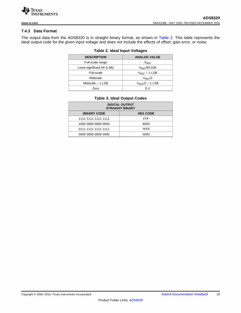
7.4.3 Data FormatThe output data from the ADS8320 is in straight binary format, as shown in Table 2. This table represents theideal output code for the given input voltage and does not include the effects of offset, gain error, or noise.
Table 2. Ideal Input VoltagesDESCRIPTION ANALOG VALUEFull-scale range VREF
Least significant bit (LSB) VREF/65,536Full-scale VREF – 1 LSBMidscale VREF/2
Midscale – 1 LSB VREF/2 – 1 LSBZero 0 V
Table 3. Ideal Output CodesDIGITAL OUTPUT
STRAIGHT BINARYBINARY CODE HEX CODE
1111 1111 1111 1111 FFF1000 0000 0000 0000 80000111 1111 1111 1111 7FFF0000 0000 0000 0000 0000

REF5030
J1
J2
J3
BoosterPack interface
BoosterPack interface
TIDA-00564
Sensorinterface LMP7716
ADS8320
3 V
10M 100
1n
+
_
SPICLK
SPI MISO
SPI CS
1.57 V
U3
U1
U2
3.3 V
3.3 V 3.3 V
T
TT
16
ADS8320SBAS108E –MAY 2000–REVISED DECEMBER 2016 www.ti.com
Product Folder Links: ADS8320
Submit Documentation Feedback Copyright © 2000–2016, Texas Instruments Incorporated
8 Application and Implementation
NOTEInformation in the following applications sections is not part of the TI componentspecification, and TI does not warrant its accuracy or completeness. TI’s customers areresponsible for determining suitability of components for their purposes. Customers shouldvalidate and test their design implementation to confirm system functionality.
8.1 Application InformationTo maximize the performance of data acquisition (DAQ) system based on a high-precision, successiveapproximation register (SAR), and analog-to-digital converter (ADC), the input driver and the reference drivercircuits must be designed properly and must be optimized. This section introduces some application circuitsdesigned using the ADS8320, and the detailed information for the some general principles designing thesecircuits can be referred to the related documentation.
8.2 Typical Applications
8.2.1 Universal Sensor IF SAR Booster Pack
Figure 22. Block Diagram for Universal Sensor IF SAR Booster Pack

17
ADS8320www.ti.com SBAS108E –MAY 2000–REVISED DECEMBER 2016
Product Folder Links: ADS8320
Submit Documentation FeedbackCopyright © 2000–2016, Texas Instruments Incorporated
Typical Applications (continued)8.2.1.1 Design RequirementsThis TI Design is a universal sensor IF based on a successive approximation register (SAR) ADC built in aBooster Pack form factor to be easily connected to TI LaunchPad for development and testing. The analog frontend (AFE) of the board has been designed for sensors with low output voltage range and high output impedancesuch as thermopiles, infrared (IR) thermometers, thermocouple amplifiers, pH electrode buffers, piezoelectricaccelerometers, and many others.
This application circuit for ADS8320 is designed to achieve the key specifications:• 16-bit 100 KHz• Low-input referred noise and low-input bias (100 fA)• Ideal choice for high-impedance output sensors
8.2.1.2 Detailed Design ProcedureThe ADS8320 was selected in this design because it best matches the design’s input requirements and highperformance. The maximum throughput rate of the ADS8320 is 100 ksps, the resolution is equal to 16 bits, andthe input range of the ADS8320 is equal to the reference voltage supplied to the converter. In this design, thereference voltage is equal to 3 V. The REF5030 features low noise, very low drift, and high initial accuracy forhigh-performance data converters. The output of the REF5030 is 3 V, which fixes the voltage range of the ADCand can provide a stable reference voltage to maintain the accuracy.
Because the system is targeted for high-impedance output sensors, CMOS or JFET input amplifiers arepreferable. The LMP7716 is a CMOS amplifier with low-input referred noise and low-input bias current, whichmake it an ideal choice for sensor interfaces such as thermopiles, IR thermometers, thermocouple amplifiers,and pH electrode buffers. To ensure the amplifier settles in enough time for the ADC to complete the signalacquisition. The gain bandwidth product of the amplifier is high enough to make sure that the input signalbandwidth is accounted for, and the amplifier is stable with the filter load. The amplifier has a fast slew rate tocharge the filter changes and to quickly react to changes of the input.
A low-pass filter must be placed between the input of the ADC and input amplifier. Choosing the capacitor andresistor values play an important role to have a good AFE design. CFLT serves two purposes. Firstly, thiscapacitor stores energy to charge the ADC internal sampling capacitor. Secondly, CFLT provides a place for theinternal capacitor’s charge to go. Due to the storage capabilities of CFLT, this design guide sometimes refers tothis capacitor as the flywheel capacitor. CFLT has this alternative name because, like a flywheel, it stores energyfor the acquisition time of the ADC. Another name used to describe CFLT is charge reservoir. This TI design hasa CFLT equal to 1 nF. This capacitor must be a high-quality capacitor with low voltage and frequencycoefficients. The recommended capacitor type is C0G. As a check, make sure the filter capacitor value chosen isat least 20 times the internal capacitor value of ADC. In this case, the value is more than 20 times the size.
The external RFLT | CFLT in the low-pass filter must settle within the ADC acquisition time. As a rule of thumb, setthe external RFLT | CFLT settling time constant a bit faster than ideal (for example, 60%) to allow a margin for errorof the op-amp load transient and the small signal settling time. TI design has an RFLT equal to 100 Ω. Thedetailed discussion and calculation can be found in Universal Sensor IF SAR BoosterPack (TIDUAI7).

Vin(V)
ER
RO
R
-15 -12 -9 -6 -3 0 3 6 9 12 15-0.0025
-0.002
-0.0015
-0.001
-0.0005
0
0.0005
0.001
0.0015
0.002
0.0025
0.003
18
ADS8320SBAS108E –MAY 2000–REVISED DECEMBER 2016 www.ti.com
Product Folder Links: ADS8320
Submit Documentation Feedback Copyright © 2000–2016, Texas Instruments Incorporated
Typical Applications (continued)8.2.1.3 Application Curves
8.2.1.3.1 Static Test (DC)
Figure 23 shows the error, which is the measured output voltage minus the ideal output voltage.
Figure 23. Error (Measured VOUT Minus Ideal VOUT) vs Input Voltage
8.2.1.3.2 Dynamic Test (AC)
For the dynamic test, sine wave is applied at the input of the board with fixed amplitude equal to –1 dBFS and avarying frequency of 0.5 kHz, 1 kHz, 5 kHz, and 10 kHz. Figure 24 shows the test result for 0.5 kHz.
Figure 24. FFT at 500 Hz (Input Signal –1 dBFS)
For step-by-step design procedure, circuit schematics, bill of materials, printed circuit board (PCB) files,simulation results, and test results, refer to TI Precision Design TIDA-00564, Universal Sensor IF SAR BoosterPack Reference Design.

TMP103Temperature
sensor
MSP430FR5969
CC2600 /6LoPan
BQ25570TPL0501
Potentiometer
TPS22969Load switch
ADS832016-bit ADC
TPS7A7LDO
Piezovibration sensor
Li-ionbattery
Flash memory
Remote monitoring(e.g. iPad)
TPL5100Nano timer
I2C
SPI
UART
Copyright © 2016, Texas Instruments Incorporated
19
ADS8320www.ti.com SBAS108E –MAY 2000–REVISED DECEMBER 2016
Product Folder Links: ADS8320
Submit Documentation FeedbackCopyright © 2000–2016, Texas Instruments Incorporated
8.2.2 Wireless Motor Monitor (WMM)
Figure 25. System Block Diagram for Wireless Motor Monitor (WMM)
8.2.2.1 Design RequirementsThis application circuit for ADS8320 is designed to achieve the key specifications:• 16-bit 100 KHz• 4-K FFT for vibration spectral• Optimized for ultra-low sleep-mode current: IQ < 45-nA (typical; BQ-harvester in smart mode)
8.2.2.2 Detailed Design ProcedureThis TI Design is inspired by the need to monitor the health of motors and machines to accurately predict andschedule maintenance (or replacement) while minimizing cost and down time during industrial production.
This design uses a Piezo vibration sensor to monitor machine vibrations, and a 16-bit precision SAR ADC,ADS8320, is connected to the Piezo shock sensor signal chain for signal acquisition. Because Piezo sensorshave high-impedance output nodes, so it’s important to carefully design the analog front-end (AFE) circuitry toreduce the noise and increase the sensitivity of the system, also drive ADS8320 and settle the signal properlyduring the acquisition time.

20
ADS8320SBAS108E –MAY 2000–REVISED DECEMBER 2016 www.ti.com
Product Folder Links: ADS8320
Submit Documentation Feedback Copyright © 2000–2016, Texas Instruments Incorporated
8.2.2.3 Application CurvesWhen testing the system with a portable speaker, the test result graph with 4-K FFT is shown in Figure 26.
Figure 26. Android Screen Shot of FFT at 600-Hz Excitation With Portable Speaker
When testing the system with a shaker calibrated with a accelerometer, the ADC is used and the AFE gain is setto 11, then configure the software to output 0.1-g of vibration at 500 KHz (or 1.5 KHz, and 2.5 KHz) as depictedin Figure 27.

21
ADS8320www.ti.com SBAS108E –MAY 2000–REVISED DECEMBER 2016
Product Folder Links: ADS8320
Submit Documentation FeedbackCopyright © 2000–2016, Texas Instruments Incorporated
Figure 27. BLE Received FFT at 500-Hz 0.1-g Excitation (X 2.4 = Hertz)
For step-by-step design procedure, circuit schematics, bill of materials, printed circuit board (PCB) files,simulation results, and test results, refer to TI Precision Design TIDM-WLMOTORMONITOR, Wireless MotorMonitor Reference Design.

22
ADS8320SBAS108E –MAY 2000–REVISED DECEMBER 2016 www.ti.com
Product Folder Links: ADS8320
Submit Documentation Feedback Copyright © 2000–2016, Texas Instruments Incorporated
9 Power Supply RecommendationsThe ADS8320 is designed to operate using a simple power supply voltage from 2.0 V to 5.25 V, but thespecifications are ensured over a 2.7-V to 5.25-V supply range. This supply must be well regulated andbypassed. A ceramic decoupling capacitor must be placed on the supply pin as close as possible to theADS8320 package. In addition, a 1-µF to 10-µF capacitor and a 5-Ω or 10-Ω series resistor may be used to low-pass filter a noisy supply.
10 Layout
10.1 Layout GuidelinesFor optimum performance, care must be taken with the physical layout of the ADS8320 circuitry. This isparticularly true if the reference voltage is low and/or the conversion rate is high. At a 100-kHz conversion rate,the ADS8320 makes a bit decision every 416 ns. That is, for each subsequent bit decision, the digital outputmust be updated with the results of the last bit decision, the capacitor array appropriately switched and charged,and the input to the comparator settled to a 16-bit level all within one clock cycle.
TI recommends following these layout guidelines:• A printed-circuit board (PCB) with at least four layers to keep all critical components on the top layer.• Analog input signals and the reference input signals must be kept away from noise sources. Crossing digital
lines with the analog signal path must be avoided. The analog input and the reference signals are routed onto the left side of the board and the digital connections are routed on the right side of the device.
• Due to the dynamic currents that occur during conversion and data transfer, the supply pin (+VCC) must havea decoupling capacitor that keeps the supply voltage stable. A 1-µF ceramic decoupling capacitor isrecommended for the supply pin.
• A layout that interconnects the converter and accompanying capacitors with the low inductance path is criticalfor achieving optimal performance. Using 15-mil vias to interconnect components to a solid analog groundplane at the subsequent inner layer minimizes stray inductance. Avoid placing vias between the supply pinand the decoupling capacitor. Any inductance between the supply capacitor and the supply pin of theconverter must be kept to less than 5 nH by placing the capacitor within 0.2 inches from the supply or inputpins of the ADS8320 and by using 20-mil traces.
• Dynamic currents are also present at the REF pin during the conversion phase. Therefore, good decoupling iscritical to achieve optimal performance. The inductance between the reference capacitor and the REF pinmust be kept to less than 2 nH by placing the capacitor within 0.1 inches from the REFIN pin and by using20-mil traces.
• A single 10-µF, X7R-grade, 0805-size ceramic capacitor with at least a 10-V rating for good performance overtemperature range.
• A small, 0.1-Ω to 0.47-Ω, 0603-size resistor placed in series with the reference capacitor keeps the overallimpedance low and constant, especially at very high frequencies.
• Avoid using additional lower value capacitors because the interactions between multiple capacitors can affectthe ADC performance at higher sampling rates.
• Place the RC filters immediately next to the input pins. Among surface-mount capacitors, COG (NPO)ceramic capacitors provide the best capacitance precision. The type of dielectric used in COG (NPO) ceramiccapacitors provides the most stable electrical properties over voltage, frequency, and temperature changes.
• The GND pin on the ADS8320 must be placed on a clean ground plane. In many cases, this is the analogground.

GND 10µF
0.1~0.47
ExternalReference
1µF
VCC
VC
C
DCLOCK
DOUT
/CS/SHDN
REF
+VCCVREF
+IN
-IN
GND
GND
47
47
47
GND
GND
23
ADS8320www.ti.com SBAS108E –MAY 2000–REVISED DECEMBER 2016
Product Folder Links: ADS8320
Submit Documentation FeedbackCopyright © 2000–2016, Texas Instruments Incorporated
10.2 Layout Example
Figure 28. Layout Example
10.3 Power DissipationThe architecture of the converter, the semiconductor fabrication process, and a careful design allow theADS8320 to convert at up to a 100kHz rate while requiring very little power. Still, for the absolute lowest powerdissipation, there are several things to keep in mind.
The power dissipation of the ADS8320 scales directly with conversion rate. Therefore, the first step to achievingthe lowest power dissipation is to find the lowest conversion rate that satisfies the requirements of the system.
In addition, the ADS8320 is in power-down mode under two conditions: when the conversion is complete andwhenever CS is HIGH (as shown in Figure 29). Ideally, each conversion must occur as quickly as possible,preferably at a 2.4-MHz clock rate. This way, the converter spends the longest possible time in the power-downmode. This is very important as the converter not only uses power on each DCLOCK transition (as is typical fordigital CMOS components), but also uses some current for the analog circuitry, such as the comparator. Theanalog section dissipates power continuously, until the power-down mode is entered.
The following timing diagrams and test circuits pertain to the parameters in Table 1.

tdDO
DOUT
DCLOCK
VOH
VOL
V IL
thDO
tr
DOUT
VOH
VOL
tf
DOUT
1.4V
Test Point
3 N�
100 pFCLOAD
Copyright © 2016, Texas Instruments Incorporated
CS/SHDN
DOUT
DCLOCK
Complete Cycle
Power DownConversionSample
Use positive clock edge for data transfer
tSUCS
tCONVtSMPL
B15
(MSB)
B14 B13 B12 B11 B10 B9 B8 B0(LSB)
B7 B1B6 B2B5 B3B4Hi-Z
0Hi-Z
tCSD
24
ADS8320SBAS108E –MAY 2000–REVISED DECEMBER 2016 www.ti.com
Product Folder Links: ADS8320
Submit Documentation Feedback Copyright © 2000–2016, Texas Instruments Incorporated
Power Dissipation (continued)
Minimum 22 clock cycles required for 16-bit conversion. Shown are 24 clock cycles.If CS remains LOW at the end of conversion, a new datastream with LSB-first is shifted out again.
Figure 29. ADS8320 Basic Timing Diagrams
Figure 30. Load Circuit for tdDO, tr, and tf
Figure 31. Voltage Waveforms for DOUT Rise and Fall Times, tr, tf
Figure 32. Voltage Waveforms for DOUT Delay Times, tdDO

41
B1 1
5
t en
/SHDN
DCLOCK
V OLDOUT
CS
/SHDN
DOUT
Waveform 1
DOUT
Waveform 2
90%
10%
V IH
tdis
CS
DOUT
Test Point
tdis Waveform 2, ten
VCC
tdis Waveform 1100 pFCLOAD
3 N�
Copyright © 2016, Texas Instruments Incorporated
25
ADS8320www.ti.com SBAS108E –MAY 2000–REVISED DECEMBER 2016
Product Folder Links: ADS8320
Submit Documentation FeedbackCopyright © 2000–2016, Texas Instruments Incorporated
Power Dissipation (continued)
Waveform 1 is for an output with internal conditions such that the output is HIGH unless disabled by the outputcontrol. (2) Waveform 2 is for an output with internal conditions such that the output is LOW unless disabled by theoutput control.
Figure 33. Load Circuit for tdDO, tr, and tf Table 1
Figure 34. Voltage Waveforms for tdis
Figure 35. Voltage Waveforms for ten
Figure 36 shows the current consumption of the ADS8320 versus sample rate. For this graph, the converter isclocked at 2.4 MHz regardless of the sample rate; CS is HIGH for the remaining sample period. Figure 37 alsoshows current consumption versus sample rate. However, in this case, the DCLOCK period is 1/24th of the sampleperiod—CS is HIGH for one DCLOCK cycle out of every 16.

1000
800
600
400
200
0.0
0.00
Sup
ply
Cur
rent
(µA
)
0.1 1 10 100
Sample Rate (kHz)
TA = 25°CVCC = 5.0VVREF = 5.0VfCLK = 24 ��ISAMPLE
CS LOW (GND)
CS HIGH (VCC)0. 250
1000
100
10
1
Sup
ply
Cur
rent
(µA)
0.1 1 10 100Sample Rate (kHz)
TA = 25°CVCC = 5.0VVREF = 5.0VfCLK = 24 ��ISAMPLE
1000
100
10
1
Supp
ly C
urre
nt (µ
A)
0.1 1 10 100Sample Rate (kHz)
VCC = 5.0VVREF = 5.0V
VCC = 2.7VVREF = 2.5V
TA = 25°CfCLK = 2.4MHz
26
ADS8320SBAS108E –MAY 2000–REVISED DECEMBER 2016 www.ti.com
Product Folder Links: ADS8320
Submit Documentation Feedback Copyright © 2000–2016, Texas Instruments Incorporated
Power Dissipation (continued)
Figure 36. Maintaining fCLK at the Highest Possible RateAllows Supply Current to Drop Linearly With Sample Rate
Figure 37. Scaling fCLK Reduces Supply Current OnlySlightly With Sample Rate
There is an important distinction between the power-down mode that is entered after a conversion is completeand the full power-down mode which is enabled when CS is HIGH. CS LOW shuts down only the analog section.The digital section is completely shut down only when CS is HIGH. Thus, if CS is left LOW at the end of aconversion and the converter is continually clocked, the power consumption is not as low as when CS is HIGH.Figure 38 shows more information.
Power dissipation can also be reduced by lowering the power-supply voltage and the reference voltage. TheADS8320 operates over a VCC range of 2 V to 5.25 V. However, at voltages below 2.7 V, the converter does notrun at a 100-kHz sample rate. See Typical Characteristics for more information regarding power supply voltageand maximum sample rate.
Shutdown current with CS LOW varies with sample rate
Figure 38. Shutdown Current With CS HIGH is 50 nA (Typically, Regardless of the Clock)
10.3.1 Short CyclingAnother way of saving power is to use the CS signal to short cycle the conversion. Because the ADS8320 placesthe latest data bit on the DOUT line as it is generated, the converter can easily be short cycled. This term meansthat the conversion can be terminated at any time. For example, if only 14 bits of the conversion result arerequired, then the conversion can be terminated (by pulling CS HIGH) after the 14th bit has been clocked out.
This technique can be used to lower the power dissipation (or to increase the conversion rate) in thoseapplications where an analog signal is being monitored until some condition becomes true. For example, if thesignal is outside a predetermined range, the full 16-bit conversion result may not be required. If so, theconversion can be terminated after the first n bits, where n might be as low as 3 or 4. This results in lower powerdissipation in both the converter and the rest of the system, as they spend more time in the power-down mode.

27
ADS8320www.ti.com SBAS108E –MAY 2000–REVISED DECEMBER 2016
Product Folder Links: ADS8320
Submit Documentation FeedbackCopyright © 2000–2016, Texas Instruments Incorporated
11 Device and Documentation Support
11.1 Documentation Support
11.1.1 Related DocumentationFor related documentation see the following:• Universal Sensor IF SAR BoosterPack (TIDUAI7)• TI Precision Design TIDU032, Capacitive Load Drive Solution using an Isolation Resistor (TIDU032)
11.2 Receiving Notification of Documentation UpdatesTo receive notification of documentation updates, navigate to the device product folder on ti.com. In the upperright corner, click on Alert me to register and receive a weekly digest of any product information that haschanged. For change details, review the revision history included in any revised document.
11.3 Community ResourcesThe following links connect to TI community resources. Linked contents are provided "AS IS" by the respectivecontributors. They do not constitute TI specifications and do not necessarily reflect TI's views; see TI's Terms ofUse.
TI E2E™ Online Community TI's Engineer-to-Engineer (E2E) Community. Created to foster collaborationamong engineers. At e2e.ti.com, you can ask questions, share knowledge, explore ideas and helpsolve problems with fellow engineers.
Design Support TI's Design Support Quickly find helpful E2E forums along with design support tools andcontact information for technical support.
11.4 TrademarksSPI, E2E are trademarks of Texas Instruments.All other trademarks are the property of their respective owners.
11.5 Electrostatic Discharge CautionThese devices have limited built-in ESD protection. The leads should be shorted together or the device placed in conductive foamduring storage or handling to prevent electrostatic damage to the MOS gates.
11.6 GlossarySLYZ022 — TI Glossary.
This glossary lists and explains terms, acronyms, and definitions.
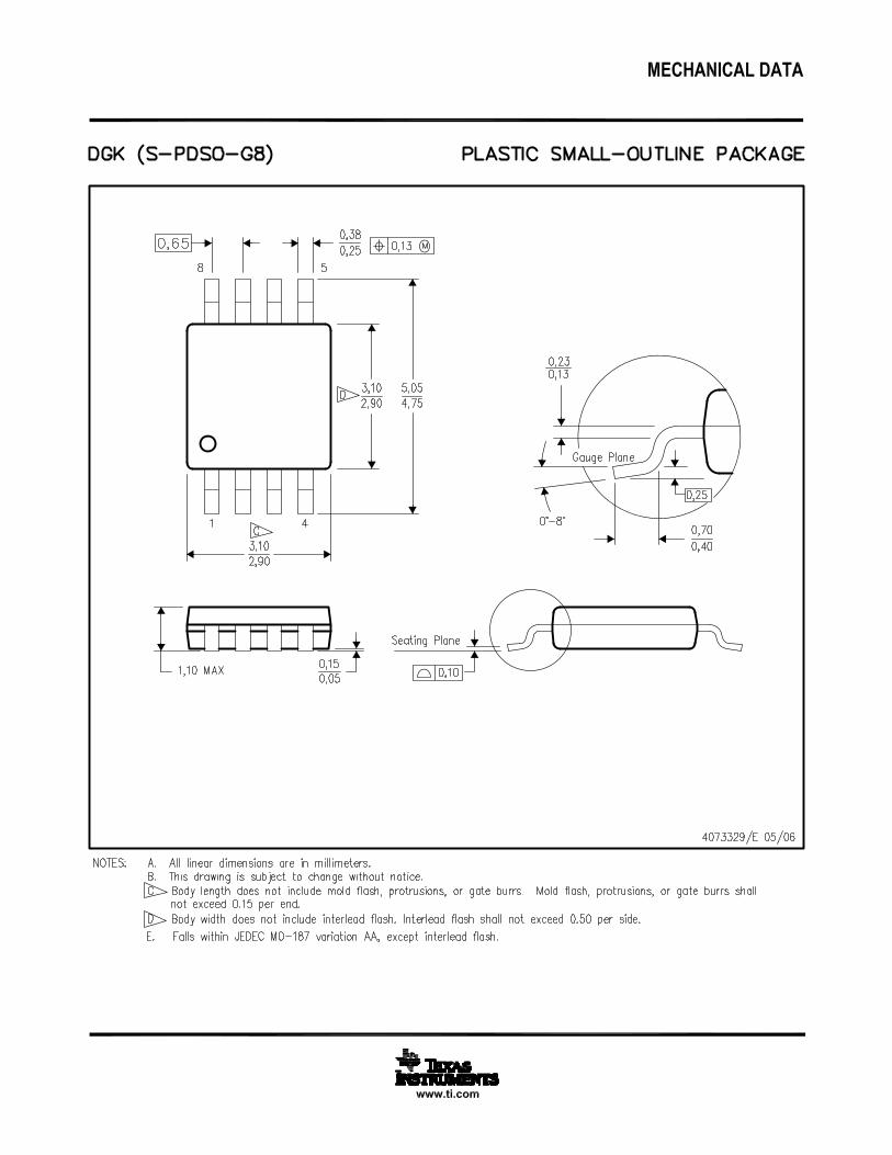
12 Mechanical, Packaging, and Orderable InformationThe following pages include mechanical, packaging, and orderable information. This information is the mostcurrent data available for the designated devices. This data is subject to change without notice and revision ofthis document. For browser-based versions of this data sheet, refer to the left-hand navigation.

PACKAGE OPTION ADDENDUM
www.ti.com 11-Jul-2017
Addendum-Page 1
PACKAGING INFORMATION
Orderable Device Status(1)
Package Type PackageDrawing
Pins PackageQty
Eco Plan(2)
Lead/Ball Finish(6)
MSL Peak Temp(3)
Op Temp (°C) Device Marking(4/5)
Samples
ADS8320E/250 ACTIVE VSSOP DGK 8 250 Green (RoHS& no Sb/Br)
CU NIPDAUAG Level-2-260C-1 YEAR -40 to 85 A20
ADS8320E/250G4 ACTIVE VSSOP DGK 8 250 Green (RoHS& no Sb/Br)
CU NIPDAUAG Level-2-260C-1 YEAR -40 to 85 A20
ADS8320E/2K5 ACTIVE VSSOP DGK 8 2500 Green (RoHS& no Sb/Br)
CU NIPDAUAG Level-2-260C-1 YEAR -40 to 85 A20
ADS8320E/2K5G4 ACTIVE VSSOP DGK 8 2500 Green (RoHS& no Sb/Br)
CU NIPDAUAG Level-2-260C-1 YEAR -40 to 85 A20
ADS8320EB/250 ACTIVE VSSOP DGK 8 250 Green (RoHS& no Sb/Br)
CU NIPDAUAG Level-2-260C-1 YEAR -40 to 85 A20
ADS8320EB/250G4 ACTIVE VSSOP DGK 8 250 Green (RoHS& no Sb/Br)
CU NIPDAUAG Level-2-260C-1 YEAR -40 to 85 A20
ADS8320EB/2K5 ACTIVE VSSOP DGK 8 2500 Green (RoHS& no Sb/Br)
CU NIPDAUAG Level-2-260C-1 YEAR -40 to 85 A20
ADS8320EB/2K5G4 ACTIVE VSSOP DGK 8 2500 Green (RoHS& no Sb/Br)
CU NIPDAUAG Level-2-260C-1 YEAR -40 to 85 A20
(1) The marketing status values are defined as follows:ACTIVE: Product device recommended for new designs.LIFEBUY: TI has announced that the device will be discontinued, and a lifetime-buy period is in effect.NRND: Not recommended for new designs. Device is in production to support existing customers, but TI does not recommend using this part in a new design.PREVIEW: Device has been announced but is not in production. Samples may or may not be available.OBSOLETE: TI has discontinued the production of the device.
(2) RoHS: TI defines "RoHS" to mean semiconductor products that are compliant with the current EU RoHS requirements for all 10 RoHS substances, including the requirement that RoHS substancedo not exceed 0.1% by weight in homogeneous materials. Where designed to be soldered at high temperatures, "RoHS" products are suitable for use in specified lead-free processes. TI mayreference these types of products as "Pb-Free".RoHS Exempt: TI defines "RoHS Exempt" to mean products that contain lead but are compliant with EU RoHS pursuant to a specific EU RoHS exemption.Green: TI defines "Green" to mean the content of Chlorine (Cl) and Bromine (Br) based flame retardants meet JS709B low halogen requirements of <=1000ppm threshold. Antimony trioxide basedflame retardants must also meet the <=1000ppm threshold requirement.
(3) MSL, Peak Temp. - The Moisture Sensitivity Level rating according to the JEDEC industry standard classifications, and peak solder temperature.
(4) There may be additional marking, which relates to the logo, the lot trace code information, or the environmental category on the device.

PACKAGE OPTION ADDENDUM
www.ti.com 11-Jul-2017
Addendum-Page 2
(5) Multiple Device Markings will be inside parentheses. Only one Device Marking contained in parentheses and separated by a "~" will appear on a device. If a line is indented then it is a continuationof the previous line and the two combined represent the entire Device Marking for that device.
(6) Lead/Ball Finish - Orderable Devices may have multiple material finish options. Finish options are separated by a vertical ruled line. Lead/Ball Finish values may wrap to two lines if the finishvalue exceeds the maximum column width.
Important Information and Disclaimer:The information provided on this page represents TI's knowledge and belief as of the date that it is provided. TI bases its knowledge and belief on informationprovided by third parties, and makes no representation or warranty as to the accuracy of such information. Efforts are underway to better integrate information from third parties. TI has taken andcontinues to take reasonable steps to provide representative and accurate information but may not have conducted destructive testing or chemical analysis on incoming materials and chemicals.TI and TI suppliers consider certain information to be proprietary, and thus CAS numbers and other limited information may not be available for release.
In no event shall TI's liability arising out of such information exceed the total purchase price of the TI part(s) at issue in this document sold by TI to Customer on an annual basis.
OTHER QUALIFIED VERSIONS OF ADS8320 :
NOTE: Qualified Version Definitions:

TAPE AND REEL INFORMATION
*All dimensions are nominal
Device PackageType
PackageDrawing
Pins SPQ ReelDiameter
(mm)
ReelWidth
W1 (mm)
A0(mm)
B0(mm)
K0(mm)
P1(mm)
W(mm)
Pin1Quadrant
ADS8320E/250 VSSOP DGK 8 250 180.0 12.4 5.3 3.4 1.4 8.0 12.0 Q1
ADS8320E/2K5 VSSOP DGK 8 2500 330.0 12.4 5.3 3.4 1.4 8.0 12.0 Q1
ADS8320EB/250 VSSOP DGK 8 250 180.0 12.4 5.3 3.4 1.4 8.0 12.0 Q1
ADS8320EB/2K5 VSSOP DGK 8 2500 330.0 12.4 5.3 3.4 1.4 8.0 12.0 Q1
PACKAGE MATERIALS INFORMATION
www.ti.com 11-Jul-2017
Pack Materials-Page 1

*All dimensions are nominal
Device Package Type Package Drawing Pins SPQ Length (mm) Width (mm) Height (mm)
ADS8320E/250 VSSOP DGK 8 250 210.0 185.0 35.0
ADS8320E/2K5 VSSOP DGK 8 2500 367.0 367.0 38.0
ADS8320EB/250 VSSOP DGK 8 250 210.0 185.0 35.0
ADS8320EB/2K5 VSSOP DGK 8 2500 367.0 367.0 38.0
PACKAGE MATERIALS INFORMATION
www.ti.com 11-Jul-2017
Pack Materials-Page 2


IMPORTANT NOTICE
Texas Instruments Incorporated (TI) reserves the right to make corrections, enhancements, improvements and other changes to itssemiconductor products and services per JESD46, latest issue, and to discontinue any product or service per JESD48, latest issue. Buyersshould obtain the latest relevant information before placing orders and should verify that such information is current and complete.TI’s published terms of sale for semiconductor products (http://www.ti.com/sc/docs/stdterms.htm) apply to the sale of packaged integratedcircuit products that TI has qualified and released to market. Additional terms may apply to the use or sale of other types of TI products andservices.Reproduction of significant portions of TI information in TI data sheets is permissible only if reproduction is without alteration and isaccompanied by all associated warranties, conditions, limitations, and notices. TI is not responsible or liable for such reproduceddocumentation. Information of third parties may be subject to additional restrictions. Resale of TI products or services with statementsdifferent from or beyond the parameters stated by TI for that product or service voids all express and any implied warranties for theassociated TI product or service and is an unfair and deceptive business practice. TI is not responsible or liable for any such statements.Buyers and others who are developing systems that incorporate TI products (collectively, “Designers”) understand and agree that Designersremain responsible for using their independent analysis, evaluation and judgment in designing their applications and that Designers havefull and exclusive responsibility to assure the safety of Designers' applications and compliance of their applications (and of all TI productsused in or for Designers’ applications) with all applicable regulations, laws and other applicable requirements. Designer represents that, withrespect to their applications, Designer has all the necessary expertise to create and implement safeguards that (1) anticipate dangerousconsequences of failures, (2) monitor failures and their consequences, and (3) lessen the likelihood of failures that might cause harm andtake appropriate actions. Designer agrees that prior to using or distributing any applications that include TI products, Designer willthoroughly test such applications and the functionality of such TI products as used in such applications.TI’s provision of technical, application or other design advice, quality characterization, reliability data or other services or information,including, but not limited to, reference designs and materials relating to evaluation modules, (collectively, “TI Resources”) are intended toassist designers who are developing applications that incorporate TI products; by downloading, accessing or using TI Resources in anyway, Designer (individually or, if Designer is acting on behalf of a company, Designer’s company) agrees to use any particular TI Resourcesolely for this purpose and subject to the terms of this Notice.TI’s provision of TI Resources does not expand or otherwise alter TI’s applicable published warranties or warranty disclaimers for TIproducts, and no additional obligations or liabilities arise from TI providing such TI Resources. TI reserves the right to make corrections,enhancements, improvements and other changes to its TI Resources. TI has not conducted any testing other than that specificallydescribed in the published documentation for a particular TI Resource.Designer is authorized to use, copy and modify any individual TI Resource only in connection with the development of applications thatinclude the TI product(s) identified in such TI Resource. NO OTHER LICENSE, EXPRESS OR IMPLIED, BY ESTOPPEL OR OTHERWISETO ANY OTHER TI INTELLECTUAL PROPERTY RIGHT, AND NO LICENSE TO ANY TECHNOLOGY OR INTELLECTUAL PROPERTYRIGHT OF TI OR ANY THIRD PARTY IS GRANTED HEREIN, including but not limited to any patent right, copyright, mask work right, orother intellectual property right relating to any combination, machine, or process in which TI products or services are used. Informationregarding or referencing third-party products or services does not constitute a license to use such products or services, or a warranty orendorsement thereof. Use of TI Resources may require a license from a third party under the patents or other intellectual property of thethird party, or a license from TI under the patents or other intellectual property of TI.TI RESOURCES ARE PROVIDED “AS IS” AND WITH ALL FAULTS. TI DISCLAIMS ALL OTHER WARRANTIES ORREPRESENTATIONS, EXPRESS OR IMPLIED, REGARDING RESOURCES OR USE THEREOF, INCLUDING BUT NOT LIMITED TOACCURACY OR COMPLETENESS, TITLE, ANY EPIDEMIC FAILURE WARRANTY AND ANY IMPLIED WARRANTIES OFMERCHANTABILITY, FITNESS FOR A PARTICULAR PURPOSE, AND NON-INFRINGEMENT OF ANY THIRD PARTY INTELLECTUALPROPERTY RIGHTS. TI SHALL NOT BE LIABLE FOR AND SHALL NOT DEFEND OR INDEMNIFY DESIGNER AGAINST ANY CLAIM,INCLUDING BUT NOT LIMITED TO ANY INFRINGEMENT CLAIM THAT RELATES TO OR IS BASED ON ANY COMBINATION OFPRODUCTS EVEN IF DESCRIBED IN TI RESOURCES OR OTHERWISE. IN NO EVENT SHALL TI BE LIABLE FOR ANY ACTUAL,DIRECT, SPECIAL, COLLATERAL, INDIRECT, PUNITIVE, INCIDENTAL, CONSEQUENTIAL OR EXEMPLARY DAMAGES INCONNECTION WITH OR ARISING OUT OF TI RESOURCES OR USE THEREOF, AND REGARDLESS OF WHETHER TI HAS BEENADVISED OF THE POSSIBILITY OF SUCH DAMAGES.Unless TI has explicitly designated an individual product as meeting the requirements of a particular industry standard (e.g., ISO/TS 16949and ISO 26262), TI is not responsible for any failure to meet such industry standard requirements.Where TI specifically promotes products as facilitating functional safety or as compliant with industry functional safety standards, suchproducts are intended to help enable customers to design and create their own applications that meet applicable functional safety standardsand requirements. Using products in an application does not by itself establish any safety features in the application. Designers mustensure compliance with safety-related requirements and standards applicable to their applications. Designer may not use any TI products inlife-critical medical equipment unless authorized officers of the parties have executed a special contract specifically governing such use.Life-critical medical equipment is medical equipment where failure of such equipment would cause serious bodily injury or death (e.g., lifesupport, pacemakers, defibrillators, heart pumps, neurostimulators, and implantables). Such equipment includes, without limitation, allmedical devices identified by the U.S. Food and Drug Administration as Class III devices and equivalent classifications outside the U.S.TI may expressly designate certain products as completing a particular qualification (e.g., Q100, Military Grade, or Enhanced Product).Designers agree that it has the necessary expertise to select the product with the appropriate qualification designation for their applicationsand that proper product selection is at Designers’ own risk. Designers are solely responsible for compliance with all legal and regulatoryrequirements in connection with such selection.Designer will fully indemnify TI and its representatives against any damages, costs, losses, and/or liabilities arising out of Designer’s non-compliance with the terms and provisions of this Notice.
Mailing Address: Texas Instruments, Post Office Box 655303, Dallas, Texas 75265Copyright © 2017, Texas Instruments Incorporated