tps2020/21/22/23/24 - power-distribution switches … · detailed description power switch charge...
TRANSCRIPT
1FEATURES
1
2
3
4
8
7
6
5
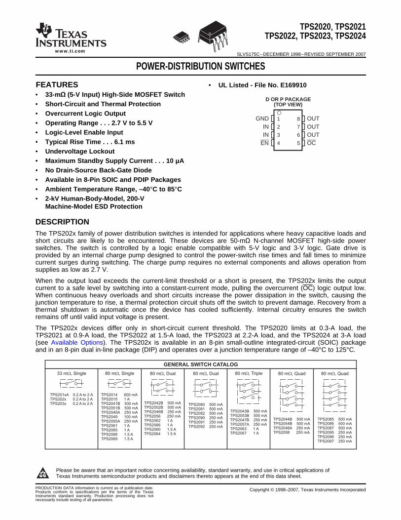
GNDININ
EN
OUTOUTOUTOC
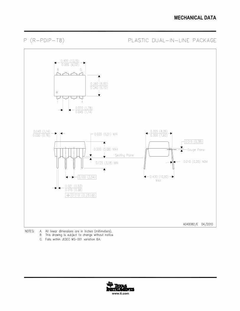
D OR P PACKAGE(TOP VIEW)
DESCRIPTION
TPS2020,, TPS2021TPS2022, TPS2023, TPS2024
SLVS175C–DECEMBER 1998–REVISED SEPTEMBER 2007www.ti.com
POWER-DISTRIBUTION SWITCHES
• UL Listed - File No. E169910• 33-mΩ (5-V Input) High-Side MOSFET Switch• Short-Circuit and Thermal Protection• Overcurrent Logic Output• Operating Range . . . 2.7 V to 5.5 V• Logic-Level Enable Input• Typical Rise Time . . . 6.1 ms• Undervoltage Lockout• Maximum Standby Supply Current . . . 10 μA• No Drain-Source Back-Gate Diode• Available in 8-Pin SOIC and PDIP Packages• Ambient Temperature Range, –40°C to 85°C• 2-kV Human-Body-Model, 200-V
Machine-Model ESD Protection
The TPS202x family of power distribution switches is intended for applications where heavy capacitive loads andshort circuits are likely to be encountered. These devices are 50-mΩ N-channel MOSFET high-side powerswitches. The switch is controlled by a logic enable compatible with 5-V logic and 3-V logic. Gate drive isprovided by an internal charge pump designed to control the power-switch rise times and fall times to minimizecurrent surges during switching. The charge pump requires no external components and allows operation fromsupplies as low as 2.7 V.
When the output load exceeds the current-limit threshold or a short is present, the TPS202x limits the outputcurrent to a safe level by switching into a constant-current mode, pulling the overcurrent (OC) logic output low.When continuous heavy overloads and short circuits increase the power dissipation in the switch, causing thejunction temperature to rise, a thermal protection circuit shuts off the switch to prevent damage. Recovery from athermal shutdown is automatic once the device has cooled sufficiently. Internal circuitry ensures the switchremains off until valid input voltage is present.
The TPS202x devices differ only in short-circuit current threshold. The TPS2020 limits at 0.3-A load, theTPS2021 at 0.9-A load, the TPS2022 at 1.5-A load, the TPS2023 at 2.2-A load, and the TPS2024 at 3-A load(see Available Options). The TPS202x is available in an 8-pin small-outline integrated-circuit (SOIC) packageand in an 8-pin dual in-line package (DIP) and operates over a junction temperature range of –40°C to 125°C.
1
Please be aware that an important notice concerning availability, standard warranty, and use in critical applications ofTexas Instruments semiconductor products and disclaimers thereto appears at the end of this data sheet.
PRODUCTION DATA information is current as of publication date. Copyright © 1998–2007, Texas Instruments IncorporatedProducts conform to specifications per the terms of the TexasInstruments standard warranty. Production processing does notnecessarily include testing of all parameters.

www.ti.com
OUT
OC
IN
EN
GND
CurrentLimit
Driver
UVLO
ChargePump
CS
ThermalSense
Power Switch
†
†Current Sense
TPS2020,, TPS2021TPS2022, TPS2023, TPS2024
SLVS175C–DECEMBER 1998–REVISED SEPTEMBER 2007
Table 1. AVAILABLE OPTIONS
PACKAGED DEVICESRECOMMENDED MAXIMUM TYPICAL SHORT-CIRCUITTA ENABLE CONTINUOUS LOAD CURRENT LIMIT AT 25°C SMALL OUTLINE PLASTIC DIP
CURRENT (A) (A) (D) (1) (P)
0.2 0.3 TPS2020D TPS2020P
0.6 0.9 TPS2021D TPS2021P
–40°C to 85°C Active low 1 1.5 TPS2022D TPS2022P
1.5 2.2 TPS2023D TPS2023P
2 3 TPS2024D TPS2024P
(1) The D package is available taped and reeled. Add an R suffix to device type (e.g., TPS2020DR)
TPS2020 FUNCTIONAL BLOCK DIAGRAM
TERMINAL FUNCTIONS
TERMINALI/O DESCRIPTIONNO.NAME D OR P
EN 4 I Enable input. Logic-low turns on power switch.
GND 1 I Ground
IN 2, 3 I Input voltage
OC 5 O Overcurrent. Logic output, active-low
OUT 6, 7, 8 O Power-switch output
2 Submit Documentation Feedback Copyright © 1998–2007, Texas Instruments Incorporated
Product Folder Link(s): TPS2020 TPS2021 TPS2022 TPS2023 TPS2024

www.ti.com
DETAILED DESCRIPTION
POWER SWITCH
CHARGE PUMP
DRIVER
ENABLE (EN)
OVERCURRENT (OC)
CURRENT SENSE
THERMAL SENSE
UNDERVOLTAGE LOCKOUT
TPS2020,, TPS2021TPS2022, TPS2023, TPS2024
SLVS175C–DECEMBER 1998–REVISED SEPTEMBER 2007
The power switch is an N-channel MOSFET with a maximum on-state resistance of 50 mΩ (VI(IN) = 5 V).Configured as a high-side switch, the power switch prevents current flow from OUT to IN and IN to OUT whendisabled.
An internal charge pump supplies power to the driver circuit and provides the necessary voltage to pull the gateof the MOSFET above the source. The charge pump operates from input voltages as low as 2.7 V and requiresvery little supply current.
The driver controls the gate voltage of the power switch. To limit large current surges and reduce the associatedelectromagnetic interference (EMI) produced, the driver incorporates circuitry that controls the rise times and falltimes of the output voltage. The rise and fall times are typically in the 2-ms to 9-ms range.
The logic enable disables the power switch, the bias for the charge pump, driver, and other circuitry to reduce thesupply current to less than 10 μA when a logic-high is present on EN. A logic-zero input on EN restores bias tothe drive and control circuits and turns the power on. The enable input is compatible with both TTL and CMOSlogic levels.
The OC open drain output is asserted (active low) when an overcurrent or overtemperature condition isencountered. The output remains asserted until the overcurrent or overtemperature condition is removed.
A sense FET monitors the current supplied to the load. The sense FET measures current more efficiently thanconventional resistance methods. When an overload or short circuit is encountered, the current-sense circuitrysends a control signal to the driver. The driver, in turn, reduces the gate voltage and drives the power FET intoits saturation region, which switches the output into a constant-current mode and holds the current constant whilevarying the voltage on the load.
An internal thermal-sense circuit shuts off the power switch when the junction temperature rises to approximately140°C. Hysteresis is built into the thermal sense circuit. After the device has cooled approximately 20°C, theswitch turns back on. The switch continues to cycle off and on until the fault is removed.
A voltage sense circuit monitors the input voltage. When the input voltage is below approximately 2 V, a controlsignal turns off the power switch.
Copyright © 1998–2007, Texas Instruments Incorporated Submit Documentation Feedback 3
Product Folder Link(s): TPS2020 TPS2021 TPS2022 TPS2023 TPS2024
www.ti.com
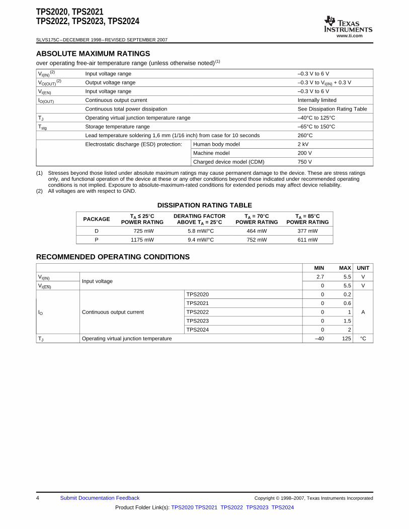
ABSOLUTE MAXIMUM RATINGS
RECOMMENDED OPERATING CONDITIONS
TPS2020,, TPS2021TPS2022, TPS2023, TPS2024
SLVS175C–DECEMBER 1998–REVISED SEPTEMBER 2007
over operating free-air temperature range (unless otherwise noted) (1)
VI(IN)(2) Input voltage range –0.3 V to 6 V
VO(OUT)(2) Output voltage range –0.3 V to VI(IN) + 0.3 V
VI(EN) Input voltage range –0.3 V to 6 V
IO(OUT) Continuous output current Internally limited
Continuous total power dissipation See Dissipation Rating Table
TJ Operating virtual junction temperature range –40°C to 125°C
Tstg Storage temperature range –65°C to 150°C
Lead temperature soldering 1,6 mm (1/16 inch) from case for 10 seconds 260°C
Electrostatic discharge (ESD) protection: Human body model 2 kV
Machine model 200 V
Charged device model (CDM) 750 V
(1) Stresses beyond those listed under absolute maximum ratings may cause permanent damage to the device. These are stress ratingsonly, and functional operation of the device at these or any other conditions beyond those indicated under recommended operatingconditions is not implied. Exposure to absolute-maximum-rated conditions for extended periods may affect device reliability.
(2) All voltages are with respect to GND.
DISSIPATION RATING TABLE
TA ≤ 25°C DERATING FACTOR TA = 70°C TA = 85°CPACKAGE POWER RATING ABOVE TA = 25°C POWER RATING POWER RATING
D 725 mW 5.8 mW/°C 464 mW 377 mW
P 1175 mW 9.4 mW/°C 752 mW 611 mW
MIN MAX UNIT
VI(IN) 2.7 5.5 VInput voltage
VI(EN) 0 5.5 V
TPS2020 0 0.2
TPS2021 0 0.6
IO Continuous output current TPS2022 0 1 A
TPS2023 0 1.5
TPS2024 0 2
TJ Operating virtual junction temperature –40 125 °C
4 Submit Documentation Feedback Copyright © 1998–2007, Texas Instruments Incorporated
Product Folder Link(s): TPS2020 TPS2021 TPS2022 TPS2023 TPS2024
www.ti.com
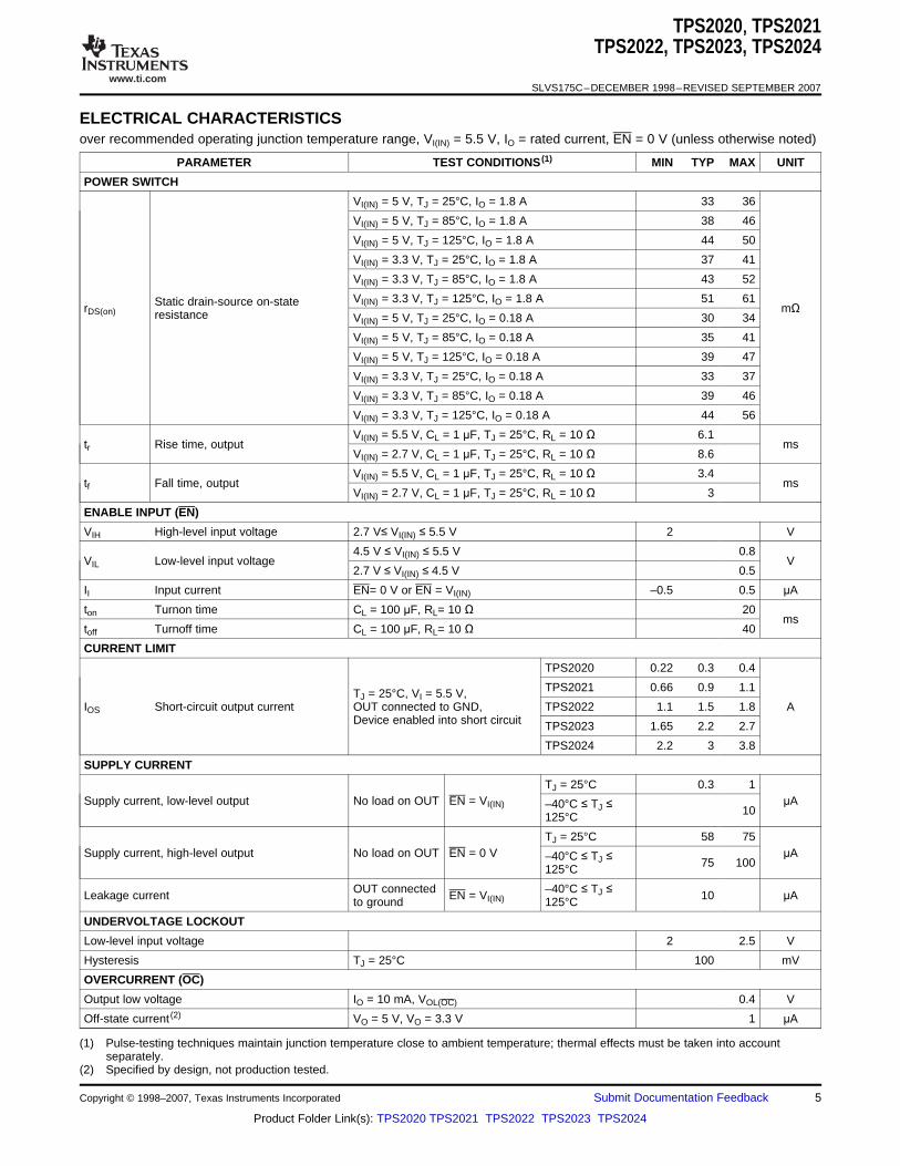
ELECTRICAL CHARACTERISTICS
TPS2020,, TPS2021TPS2022, TPS2023, TPS2024
SLVS175C–DECEMBER 1998–REVISED SEPTEMBER 2007
over recommended operating junction temperature range, VI(IN) = 5.5 V, IO = rated current, EN = 0 V (unless otherwise noted)
PARAMETER TEST CONDITIONS (1) MIN TYP MAX UNIT
POWER SWITCH
VI(IN) = 5 V, TJ = 25°C, IO = 1.8 A 33 36
VI(IN) = 5 V, TJ = 85°C, IO = 1.8 A 38 46
VI(IN) = 5 V, TJ = 125°C, IO = 1.8 A 44 50
VI(IN) = 3.3 V, TJ = 25°C, IO = 1.8 A 37 41
VI(IN) = 3.3 V, TJ = 85°C, IO = 1.8 A 43 52
VI(IN) = 3.3 V, TJ = 125°C, IO = 1.8 A 51 61Static drain-source on-staterDS(on) mΩresistance VI(IN) = 5 V, TJ = 25°C, IO = 0.18 A 30 34
VI(IN) = 5 V, TJ = 85°C, IO = 0.18 A 35 41
VI(IN) = 5 V, TJ = 125°C, IO = 0.18 A 39 47
VI(IN) = 3.3 V, TJ = 25°C, IO = 0.18 A 33 37
VI(IN) = 3.3 V, TJ = 85°C, IO = 0.18 A 39 46
VI(IN) = 3.3 V, TJ = 125°C, IO = 0.18 A 44 56
VI(IN) = 5.5 V, CL = 1 μF, TJ = 25°C, RL = 10 Ω 6.1tr Rise time, output ms
VI(IN) = 2.7 V, CL = 1 μF, TJ = 25°C, RL = 10 Ω 8.6
VI(IN) = 5.5 V, CL = 1 μF, TJ = 25°C, RL = 10 Ω 3.4tf Fall time, output ms
VI(IN) = 2.7 V, CL = 1 μF, TJ = 25°C, RL = 10 Ω 3
ENABLE INPUT (EN)
VIH High-level input voltage 2.7 V≤ VI(IN) ≤ 5.5 V 2 V
4.5 V ≤ VI(IN) ≤ 5.5 V 0.8VIL Low-level input voltage V
2.7 V ≤ VI(IN) ≤ 4.5 V 0.5
II Input current EN= 0 V or EN = VI(IN) –0.5 0.5 μA
ton Turnon time CL = 100 μF, RL= 10 Ω 20ms
toff Turnoff time CL = 100 μF, RL= 10 Ω 40
CURRENT LIMIT
TPS2020 0.22 0.3 0.4
TPS2021 0.66 0.9 1.1TJ = 25°C, VI = 5.5 V,IOS Short-circuit output current OUT connected to GND, TPS2022 1.1 1.5 1.8 A
Device enabled into short circuit TPS2023 1.65 2.2 2.7
TPS2024 2.2 3 3.8
SUPPLY CURRENT
TJ = 25°C 0.3 1Supply current, low-level output No load on OUT EN = VI(IN) μA–40°C ≤ TJ ≤ 10125°C
TJ = 25°C 58 75Supply current, high-level output No load on OUT EN = 0 V μA–40°C ≤ TJ ≤ 75 100125°C
OUT connected –40°C ≤ TJ ≤Leakage current EN = VI(IN) 10 μAto ground 125°C
UNDERVOLTAGE LOCKOUT
Low-level input voltage 2 2.5 V
Hysteresis TJ = 25°C 100 mV
OVERCURRENT (OC)
Output low voltage IO = 10 mA, VOL(OC) 0.4 V
Off-state current (2) VO = 5 V, VO = 3.3 V 1 μA
(1) Pulse-testing techniques maintain junction temperature close to ambient temperature; thermal effects must be taken into accountseparately.
(2) Specified by design, not production tested.
Copyright © 1998–2007, Texas Instruments Incorporated Submit Documentation Feedback 5
Product Folder Link(s): TPS2020 TPS2021 TPS2022 TPS2023 TPS2024
www.ti.com
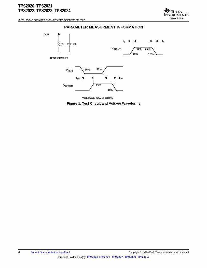
PARAMETER MEASURMENT INFORMATION
RL CL
OUT
tr tf
90% 90%
10%10%
50% 50%
90%
10%
VO(OUT)
VI(EN)
VO(OUT)
VOLTAGE WAVEFORMS
TEST CIRCUIT
ton toff
TPS2020,, TPS2021TPS2022, TPS2023, TPS2024
SLVS175C–DECEMBER 1998–REVISED SEPTEMBER 2007
Figure 1. Test Circuit and Voltage Waveforms
6 Submit Documentation Feedback Copyright © 1998–2007, Texas Instruments Incorporated
Product Folder Link(s): TPS2020 TPS2021 TPS2022 TPS2023 TPS2024

www.ti.com
TABLE OF TIMING DIAGRAMS
2 4 6 8 10 12 14 16 18 20
t − Time − ms
0
VIN = 5 VRL = 27 ΩTA = 25°C
VO(OUT) (2 V/div)
VI(EN)
VO(OUT)
VI(EN) (5 V/div)
2 4 6 8 10 12 14 16 18 20
t − Time − ms
VI(EN) (5 V/div)
0
VI(IN) = 5 VRL = 27 ΩTA = 25°C
VO(OUT) (2 V/div)
VI(EN)
VO(OUT)
TPS2020,, TPS2021TPS2022, TPS2023, TPS2024
SLVS175C–DECEMBER 1998–REVISED SEPTEMBER 2007
PARAMETER MEASURMENT INFORMATION (continued)
FIGURE
Turnon Delay and Rise TIme 2
Turnoff Delay and Fall Time 3
Turnon Delay and Rise TIme with 1-μF Load 4
Turnoff Delay and Rise TIme with 1-μF Load 5
Device Enabled into Short 6
7, 8, 9, 10,TPS2020, TPS2021, TPS2022, TPS2023, and TPS2024, Ramped Load on Enabled Device 11
TPS2024, Inrush Current 12
7.9-Ω Load Connected to an Enabled TPS2020 Device 13
3.7-Ω Load Connected to an Enabled TPS2020 Device 14
3.7-Ω Load Connected to an Enabled TPS2021 Device 15
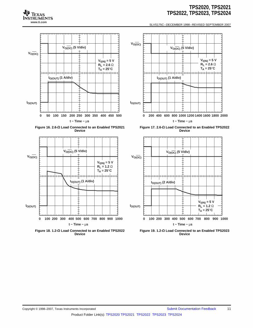
2.6-Ω Load Connected to an Enabled TPS2021 Device 16
2.6-Ω Load Connected to an Enabled TPS2022 Device 17
1.2-Ω Load Connected to an Enabled TPS2022 Device 18
1.2-Ω Load Connected to an Enabled TPS2023 Device 19
0.9-Ω Load Connected to an Enabled TPS2023 Device 20
0.9-Ω Load Connected to an Enabled TPS2024 Device 21
0.5-Ω Load Connected to an Enabled TPS2024 Device 22
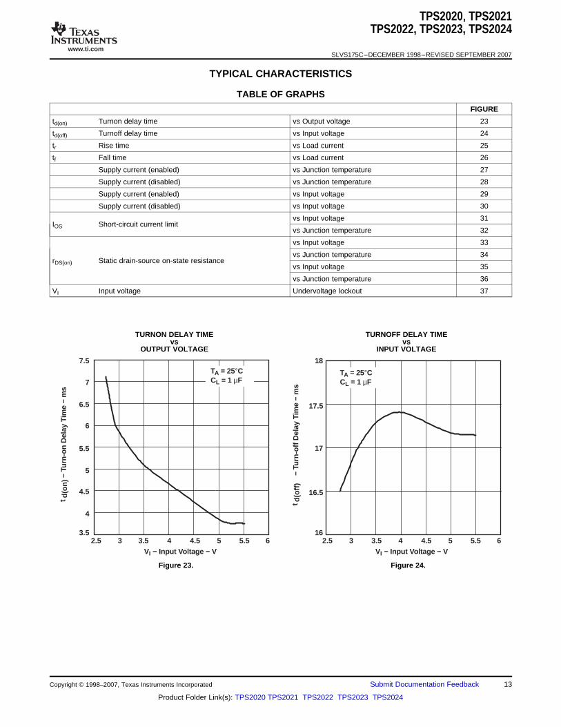
Figure 2. Turnon Delay and Rise Time Figure 3. Turnoff Delay and Fall Time
Copyright © 1998–2007, Texas Instruments Incorporated Submit Documentation Feedback 7
Product Folder Link(s): TPS2020 TPS2021 TPS2022 TPS2023 TPS2024

www.ti.com
2 4 6 8 10 12 14 16 18 20
t − Time − ms
VI(EN) (5 V/div)
0
VI(IN) = 5 VCL = 1 µFRL = 27 ΩTA = 25°C
VO(OUT) (2 V/div)
VI(EN)
VO(OUT)
2 4 6 8 10 12 14 16 18 20
t − Time − ms
VI(EN) (5 V/div)
0
VI(IN) = 5 VCL = 1 µFRL = 27 ΩTA = 25°C
VO(OUT) (2 V/div)
VI(EN)
VO(OUT)
1 2 3 4 5 6 7 8 9 10
t − Time − ms
VI(EN) (5 V/div)
0
IO(OUT) (1 A/div)
VI(EN)
IO(OUT)
VI(IN) = 5 VTA = 25°C
TPS2024
TPS2023
TPS2022
TPS2021
TPS2020
20 40 60 80 100 120 140 160 180 200
t − Time − ms
VO(OC) (5 V/div)
0
IO(OUT) (500 mA/div)
VO(OC)
IO(OUT)
VI(IN) = 5 VTA = 25°C
TPS2020,, TPS2021TPS2022, TPS2023, TPS2024
SLVS175C–DECEMBER 1998–REVISED SEPTEMBER 2007
Figure 4. Turnon Delay and Rise Time with 1-μF Load Figure 5. Turnoff Delay and Fall Time with 1-μF Load
Figure 6. Device Enabled Into Short Figure 7. TPS2020, Ramped Load on Enabled Device
8 Submit Documentation Feedback Copyright © 1998–2007, Texas Instruments Incorporated
Product Folder Link(s): TPS2020 TPS2021 TPS2022 TPS2023 TPS2024

www.ti.com
20 40 60 80 100 120 140 160 180 200
t − Time − ms
VO(OC) (5 V/div)
0
IO(OUT) (1 A/div)
VO(OC)
IO(OUT)
VI(IN) = 5 VTA = 25°C
20 40 60 80 100 120 140 160 180 200
t − Time − ms
VO(OC) (5 V/div)
0
IO(OUT) (1 A/div)
VO(OC)
IO(OUT)
VI(IN) = 5 VTA = 25°C
20 40 60 80 100 120 140 160 180 200
t − Time − ms
VO(OC) (5 V/div)
0
IO(OUT) (1 A/div)
VO(OC)
IO(OUT)
VI(IN) = 5 VTA = 25°C
20 40 60 80 100 120 140 160 180 200
t − Time − ms
VO(OC) (5 V/div)
0
IO(OUT) (1 A/div)
VO(OC)
IO(OUT)
VI(IN) = 5 VTA = 25°C
TPS2020,, TPS2021TPS2022, TPS2023, TPS2024
SLVS175C–DECEMBER 1998–REVISED SEPTEMBER 2007
Figure 8. TPS2021, Ramped Load on Enabled Device Figure 9. TPS2022, Ramped Load on Enabled Device
Figure 10. TPS2023, Ramped Load on Enabled Device Figure 11. TPS2024, Ramped Load on Enabled Device
Copyright © 1998–2007, Texas Instruments Incorporated Submit Documentation Feedback 9
Product Folder Link(s): TPS2020 TPS2021 TPS2022 TPS2023 TPS2024

www.ti.com
1 2 3 4 5 6 7 8 9 10
t − Time − ms
0
II(IN) (500 mA/div)
VI(EN)
II(IN) RL = 10 ΩTA = 25°C
VI(EN) (5 V/div)
470 µF
47 µF
150 µF
200 400 600 800 1000 1200 1400 1600 1800 2000
t − Time − µs
VO(OC) (5 V/div)
0
IO(OUT) (200 mA/div)
VO(OC)
IO(OUT)
VI(IN) = 5 VRL = 7.9 ΩTA = 25°C
50 100 150 200 250 300 350 400 450 500
t − Time − µs
VO(OC) (5 V/div)
0
IO(OUT) (500 mA/div)
VO(OC)
IO(OUT)
VI(IN) = 5 VRL = 3.7 ΩTA = 25°C
200 400 600 800 1000 1200 1400 1600 1800 2000
t − Time − µs
VO(OC) (5 V/div)
0
IO(OUT) (1 A/div)
VO(OC)
IO(OUT)
VI(IN) = 5 VRL = 3.7 ΩTA = 25°C
TPS2020,, TPS2021TPS2022, TPS2023, TPS2024
SLVS175C–DECEMBER 1998–REVISED SEPTEMBER 2007
Figure 12. TPS2024, Inrush Current Figure 13. 7.9-Ω Load Connected to an Enabled TPS2020Device
Figure 14. 3.7-Ω Load Connected to an Enabled TPS2020 Figure 15. 3.7-Ω Load Connected to an Enabled TPS2021Device Device
10 Submit Documentation Feedback Copyright © 1998–2007, Texas Instruments Incorporated
Product Folder Link(s): TPS2020 TPS2021 TPS2022 TPS2023 TPS2024
www.ti.com
50 100 150 200 250 300 350 400 450 500
t − Time − µs
VO(OC) (5 V/div)
0
IO(OUT) (1 A/div)
VO(OC)
IO(OUT)
VI(IN) = 5 VRL = 2.6 ΩTA = 25°C
200 400 600 800 1000 1200 1400 1600 1800 2000
t − Time − µs
VO(OC) (5 V/div)
0
IO(OUT) (1 A/div)
VO(OC)
IO(OUT)
VI(IN) = 5 VRL = 2.6 ΩTA = 25°C
100 200 300 400 500 600 700 800 900 1000
t − Time − µs
VO(OC) (5 V/div)
0
IO(OUT) (1 A/div)
VO(OC)
IO(OUT)
VI(IN) = 5 VRL = 1.2 ΩTA = 25°C
100 200 300 400 500 600 700 800 900 1000
t − Time − µs
VO(OC) (5 V/div)
0
IO(OUT) (2 A/div)
VO(OC)
IO(OUT)
VI(IN) = 5 VRL = 1.2 ΩTA = 25°C
TPS2020,, TPS2021TPS2022, TPS2023, TPS2024
SLVS175C–DECEMBER 1998–REVISED SEPTEMBER 2007
Figure 16. 2.6-Ω Load Connected to an Enabled TPS2021 Figure 17. 2.6-Ω Load Connected to an Enabled TPS2022Device Device
Figure 18. 1.2-Ω Load Connected to an Enabled TPS2022 Figure 19. 1.2-Ω Load Connected to an Enabled TPS2023Device Device
Copyright © 1998–2007, Texas Instruments Incorporated Submit Documentation Feedback 11
Product Folder Link(s): TPS2020 TPS2021 TPS2022 TPS2023 TPS2024

www.ti.com
100 200 300 400 500 600 700 800 900 1000
t − Time − µs
VO(OC) (5 V/div)
0
IO(OUT) (2 A/div)
VO(OC)
IO(OUT)
VI(IN) = 5 VRL = 0.9 ΩTA = 25°C
100 200 300 400 500 600 700 800 900 1000
t − Time − µs
VO(OC) (5 V/div)
0
IO(OUT) (5 A/div)
VO(OC)
IO(OUT)
VI(IN) = 5 VRL = 0.9 ΩTA = 25°C
50 100 150 200 250 300 350 400 450 500
t − Time − µs
VO(OC) (5 V/div)
0
IO(OUT) (5 A/div)
VO(OC)
IO(OUT)
VI(IN) = 5 VRL = 0.5 ΩTA = 25°C
TPS2020,, TPS2021TPS2022, TPS2023, TPS2024
SLVS175C–DECEMBER 1998–REVISED SEPTEMBER 2007
Figure 20. 0.9-Ω Load Connected to an Enabled TPS2023 Figure 21. 0.9-Ω Load Connected to an Enabled TPS2024Device Device
Figure 22. 0.5-Ω Load Connected to an Enabled TPS2024Device
12 Submit Documentation Feedback Copyright © 1998–2007, Texas Instruments Incorporated
Product Folder Link(s): TPS2020 TPS2021 TPS2022 TPS2023 TPS2024
www.ti.com
TYPICAL CHARACTERISTICS
4.5
4
3.52.5 3 3.5 4 4.5
− Tu
rn-o
n D
elay
Tim
e −
ms
5
5.5
7.5
5 5.5 6VI − Input V oltage − V
t d(o
n)
6
6.5
7
TA = 25°CCL = 1 µF
17
16.5
162.5 3 3.5 4 4.5
17.5
18
5 5.5 6VI − Input V oltage − V
− Tu
rn-o
ff D
elay
Tim
e −
ms
t d(o
ff)
TA = 25°CCL = 1 µF
TPS2020,, TPS2021TPS2022, TPS2023, TPS2024
SLVS175C–DECEMBER 1998–REVISED SEPTEMBER 2007
TABLE OF GRAPHS
FIGURE
td(on) Turnon delay time vs Output voltage 23
td(off) Turnoff delay time vs Input voltage 24
tr Rise time vs Load current 25
tf Fall time vs Load current 26
Supply current (enabled) vs Junction temperature 27
Supply current (disabled) vs Junction temperature 28
Supply current (enabled) vs Input voltage 29
Supply current (disabled) vs Input voltage 30
vs Input voltage 31IOS Short-circuit current limit
vs Junction temperature 32
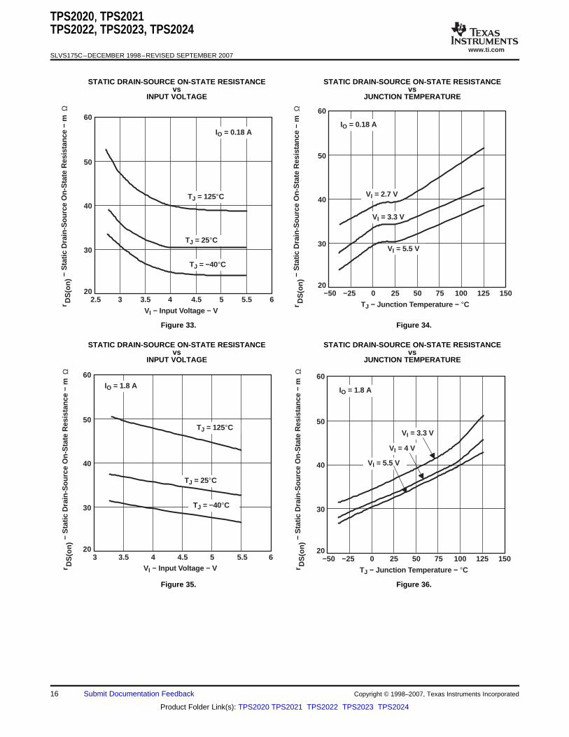
vs Input voltage 33
vs Junction temperature 34rDS(on) Static drain-source on-state resistance
vs Input voltage 35
vs Junction temperature 36
VI Input voltage Undervoltage lockout 37
TURNON DELAY TIME TURNOFF DELAY TIMEvs vs
OUTPUT VOLTAGE INPUT VOLTAGE
Figure 23. Figure 24.
Copyright © 1998–2007, Texas Instruments Incorporated Submit Documentation Feedback 13
Product Folder Link(s): TPS2020 TPS2021 TPS2022 TPS2023 TPS2024
www.ti.com
3.25
2.75
2.50 0.5
− F
all T
ime
− m
s
3.5
1 1.5 2
3
IL − Load Current − At f
TA = 25°CCL = 1 µF
5.5
50 0.5 1
− R
ise
Tim
e −
ms 6
6.5
1.5 2IL − Load Current − A
t r
TA = 25°CCL = 1 µF
55
45
35−50 −25 0 25 50
65
75
75 100 150TJ − Junction T emperature − °C
Sup
ply
Cur
rent
(Ena
bled
) −
Aµ
125
VI(IN) = 3.3 V
VI(IN) = 4 V
VI(IN) = 5 V
VI(IN) = 5.5 V
VI(IN) = 2.7 V
1
0
−1−50 −25 0 25 50
4
5
75 100 150
TJ − Junction T emperature − °C
Sup
ply
Cur
rent
(Dis
able
d) −
Aµ
125
3
2
VI(IN) = 4 V
VI(IN) = 2.7 V
VI(IN) = 5 VVI(IN) = 5.5 V
VI(IN) = 3.3 V
TPS2020,, TPS2021TPS2022, TPS2023, TPS2024
SLVS175C–DECEMBER 1998–REVISED SEPTEMBER 2007
RISE TIME FALL TIMEvs vs
LOAD CURRENT LOAD CURRENT
Figure 25. Figure 26.
SUPPLY CURRENT (ENABLED) SUPPLY CURRENT (DISABLED)vs vs
JUNCTION TEMPERATURE JUNCTION TEMPERATURE
Figure 27. Figure 28.
14 Submit Documentation Feedback Copyright © 1998–2007, Texas Instruments Incorporated
Product Folder Link(s): TPS2020 TPS2021 TPS2022 TPS2023 TPS2024

www.ti.com
55
45
352.5 3 3.5 4 4.5
65
75
5 5.5 6VI − Input V oltage − V
Sup
ply
Cur
rent
(Ena
bled
) −
Aµ
TJ = 125°C
TJ = 85°C
TJ = 25°C
TJ = 0°C
TJ = −40°C
1
0
−12.5 3 3.5 4 4.5
4
5
5 5.5 6
VI − Input V oltage − VS
uppl
y C
urre
nt (D
isab
led)
−A
µ
3
2 TJ = 85°C
TJ = 0°CTJ = −40°C
TJ = 125°C
TJ = 25°C
1.5
0.5
02 3 4
2.5
3.5
5 6VI − Input V oltage − V
− S
hort-
Circ
uit C
urre
nt L
imit
− A
I OS
1
2
3
TPS2023
TPS2022
TPS2021
TPS2020
TPS2024TA = 25°C
1.5
0.5
0−50 −25 0
2.5
3.5
25 100
TJ − Junction T emperature − °C
− S
hort-
Circ
uit C
urre
nt L
imit
− A
I OS
1
2
3
TPS2023
TPS2022
TPS2021
TPS2020
TPS2024
50 75
TPS2020,, TPS2021TPS2022, TPS2023, TPS2024
SLVS175C–DECEMBER 1998–REVISED SEPTEMBER 2007
SUPPLY CURRENT (ENABLED) SUPPLY CURRENT (DISABLED)vs vs
INPUT VOLTAGE INPUT VOLTAGE
Figure 29. Figure 30.
SHORT-CIRCUIT CURRENT LIMIT SHORT-CIRCUIT CURRENT LIMITvs vs
INPUT VOLTAGE JUNCTION TEMPERATURE
Figure 31. Figure 32.
Copyright © 1998–2007, Texas Instruments Incorporated Submit Documentation Feedback 15
Product Folder Link(s): TPS2020 TPS2021 TPS2022 TPS2023 TPS2024
www.ti.com
20−50 −25 0
40
60
25 150
TJ − Junction T emperature − °C
30
50
VI = 2.7 V
50 75 100 125
VI = 3.3 V
VI = 5.5 V
IO = 0.18 A
Ωr D
S(o
n)−
Sta
tic D
rain
-Sou
rce
On-
Sta
te R
esis
tanc
e −
m20
2.5 3 3.5
40
60
4 6
VI − Input V oltage − V
30
50
4.5 5
Ωr D
S(o
n)−
Sta
tic D
rain
-Sou
rce
On-
Sta
te R
esis
tanc
e −
m
5.5
TJ = 25°C
TJ = 125°C
TJ = −40°C
IO = 0.18 A
203 3.5
40
60
4 6VI − Input V oltage − V
30
50
4.5 5 5.5
TJ = 25°C
TJ = 125°C
IO = 1.8 A
TJ = −40°C
Ωr D
S(o
n)−
Sta
tic D
rain
-Sou
rce
On-
Sta
te R
esis
tanc
e −
m
20−50 −25 0
40
60
25 150
TJ − Junction T emperature − °C
30
50
VI = 3.3 V
50 75 100 125
VI = 4 V
VI = 5.5 V
IO = 1.8 A
Ωr D
S(o
n)−
Sta
tic D
rain
-Sou
rce
On-
Sta
te R
esis
tanc
e −
m
TPS2020,, TPS2021TPS2022, TPS2023, TPS2024
SLVS175C–DECEMBER 1998–REVISED SEPTEMBER 2007
STATIC DRAIN-SOURCE ON-STATE RESISTANCE STATIC DRAIN-SOURCE ON-STATE RESISTANCEvs vs
INPUT VOLTAGE JUNCTION TEMPERATURE
Figure 33. Figure 34.
STATIC DRAIN-SOURCE ON-STATE RESISTANCE STATIC DRAIN-SOURCE ON-STATE RESISTANCEvs vs
INPUT VOLTAGE JUNCTION TEMPERATURE
Figure 35. Figure 36.
16 Submit Documentation Feedback Copyright © 1998–2007, Texas Instruments Incorporated
Product Folder Link(s): TPS2020 TPS2021 TPS2022 TPS2023 TPS2024
www.ti.com
2−50 0 50 100
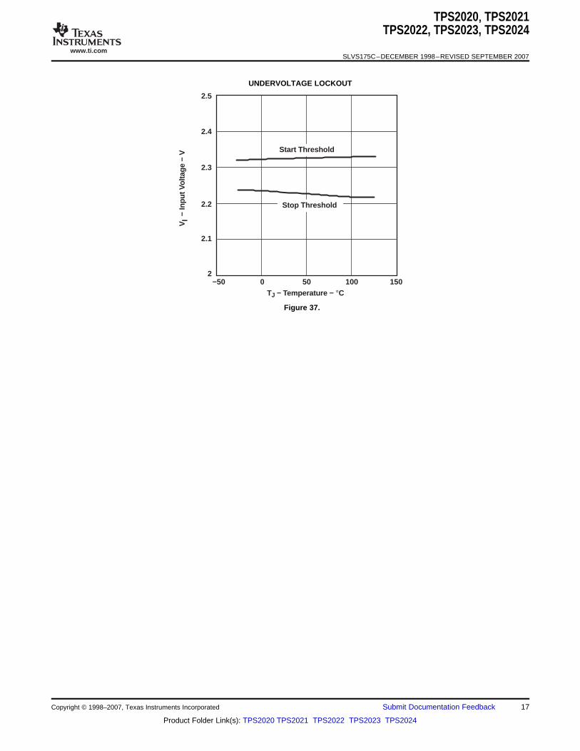
2.4
2.5
150TJ − Temperature − °C
2.3
2.2
Start Threshold
Stop Threshold
2.1
VI
− In
put V
olta
ge −
V
TPS2020,, TPS2021TPS2022, TPS2023, TPS2024
SLVS175C–DECEMBER 1998–REVISED SEPTEMBER 2007
UNDERVOLTAGE LOCKOUT
Figure 37.
Copyright © 1998–2007, Texas Instruments Incorporated Submit Documentation Feedback 17
Product Folder Link(s): TPS2020 TPS2021 TPS2022 TPS2023 TPS2024
www.ti.com
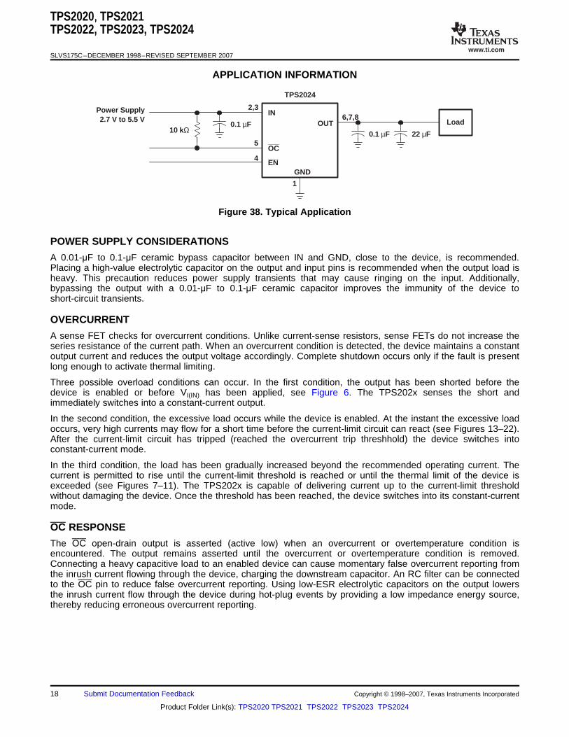
APPLICATION INFORMATION
IN
OC
ENGND
0.1 µF
2,3
5
4
6,7,8
0.1 µF 22 µF
Load
1
OUT
TPS2024
Power Supply2.7 V to 5.5 V
10 kΩ
POWER SUPPLY CONSIDERATIONS
OVERCURRENT
OC RESPONSE
TPS2020,, TPS2021TPS2022, TPS2023, TPS2024
SLVS175C–DECEMBER 1998–REVISED SEPTEMBER 2007
Figure 38. Typical Application
A 0.01-μF to 0.1-μF ceramic bypass capacitor between IN and GND, close to the device, is recommended.Placing a high-value electrolytic capacitor on the output and input pins is recommended when the output load isheavy. This precaution reduces power supply transients that may cause ringing on the input. Additionally,bypassing the output with a 0.01-μF to 0.1-μF ceramic capacitor improves the immunity of the device toshort-circuit transients.
A sense FET checks for overcurrent conditions. Unlike current-sense resistors, sense FETs do not increase theseries resistance of the current path. When an overcurrent condition is detected, the device maintains a constantoutput current and reduces the output voltage accordingly. Complete shutdown occurs only if the fault is presentlong enough to activate thermal limiting.
Three possible overload conditions can occur. In the first condition, the output has been shorted before thedevice is enabled or before VI(IN) has been applied, see Figure 6. The TPS202x senses the short andimmediately switches into a constant-current output.
In the second condition, the excessive load occurs while the device is enabled. At the instant the excessive loadoccurs, very high currents may flow for a short time before the current-limit circuit can react (see Figures 13–22).After the current-limit circuit has tripped (reached the overcurrent trip threshhold) the device switches intoconstant-current mode.
In the third condition, the load has been gradually increased beyond the recommended operating current. Thecurrent is permitted to rise until the current-limit threshold is reached or until the thermal limit of the device isexceeded (see Figures 7–11). The TPS202x is capable of delivering current up to the current-limit thresholdwithout damaging the device. Once the threshold has been reached, the device switches into its constant-currentmode.
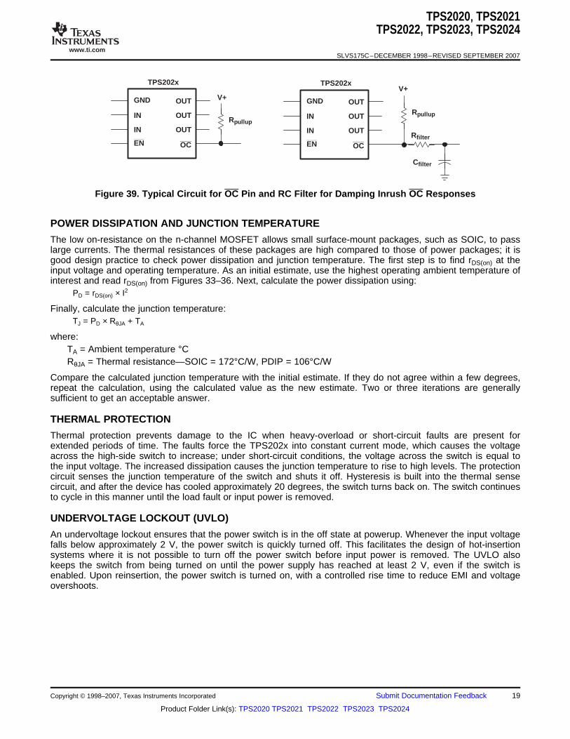
The OC open-drain output is asserted (active low) when an overcurrent or overtemperature condition isencountered. The output remains asserted until the overcurrent or overtemperature condition is removed.Connecting a heavy capacitive load to an enabled device can cause momentary false overcurrent reporting fromthe inrush current flowing through the device, charging the downstream capacitor. An RC filter can be connectedto the OC pin to reduce false overcurrent reporting. Using low-ESR electrolytic capacitors on the output lowersthe inrush current flow through the device during hot-plug events by providing a low impedance energy source,thereby reducing erroneous overcurrent reporting.
18 Submit Documentation Feedback Copyright © 1998–2007, Texas Instruments Incorporated
Product Folder Link(s): TPS2020 TPS2021 TPS2022 TPS2023 TPS2024
www.ti.com
GND
IN
IN
EN
OUT
OC
OUT
OUT
TPS202x
GND
IN
IN
EN
OUT
OC
OUT
OUT
TPS202x
Rpullup
V+
Rfilter
Rpullup
Cfilter
V+
POWER DISSIPATION AND JUNCTION TEMPERATURE
THERMAL PROTECTION
UNDERVOLTAGE LOCKOUT (UVLO)
TPS2020,, TPS2021TPS2022, TPS2023, TPS2024
SLVS175C–DECEMBER 1998–REVISED SEPTEMBER 2007
Figure 39. Typical Circuit for OC Pin and RC Filter for Damping Inrush OC Responses
The low on-resistance on the n-channel MOSFET allows small surface-mount packages, such as SOIC, to passlarge currents. The thermal resistances of these packages are high compared to those of power packages; it isgood design practice to check power dissipation and junction temperature. The first step is to find rDS(on) at theinput voltage and operating temperature. As an initial estimate, use the highest operating ambient temperature ofinterest and read rDS(on) from Figures 33–36. Next, calculate the power dissipation using:
PD = rDS(on) × I2
Finally, calculate the junction temperature:TJ = PD × RθJA + TA
where:TA = Ambient temperature °CRθJA = Thermal resistance—SOIC = 172°C/W, PDIP = 106°C/W
Compare the calculated junction temperature with the initial estimate. If they do not agree within a few degrees,repeat the calculation, using the calculated value as the new estimate. Two or three iterations are generallysufficient to get an acceptable answer.
Thermal protection prevents damage to the IC when heavy-overload or short-circuit faults are present forextended periods of time. The faults force the TPS202x into constant current mode, which causes the voltageacross the high-side switch to increase; under short-circuit conditions, the voltage across the switch is equal tothe input voltage. The increased dissipation causes the junction temperature to rise to high levels. The protectioncircuit senses the junction temperature of the switch and shuts it off. Hysteresis is built into the thermal sensecircuit, and after the device has cooled approximately 20 degrees, the switch turns back on. The switch continuesto cycle in this manner until the load fault or input power is removed.
An undervoltage lockout ensures that the power switch is in the off state at powerup. Whenever the input voltagefalls below approximately 2 V, the power switch is quickly turned off. This facilitates the design of hot-insertionsystems where it is not possible to turn off the power switch before input power is removed. The UVLO alsokeeps the switch from being turned on until the power supply has reached at least 2 V, even if the switch isenabled. Upon reinsertion, the power switch is turned on, with a controlled rise time to reduce EMI and voltageovershoots.
Copyright © 1998–2007, Texas Instruments Incorporated Submit Documentation Feedback 19
Product Folder Link(s): TPS2020 TPS2021 TPS2022 TPS2023 TPS2024
www.ti.com
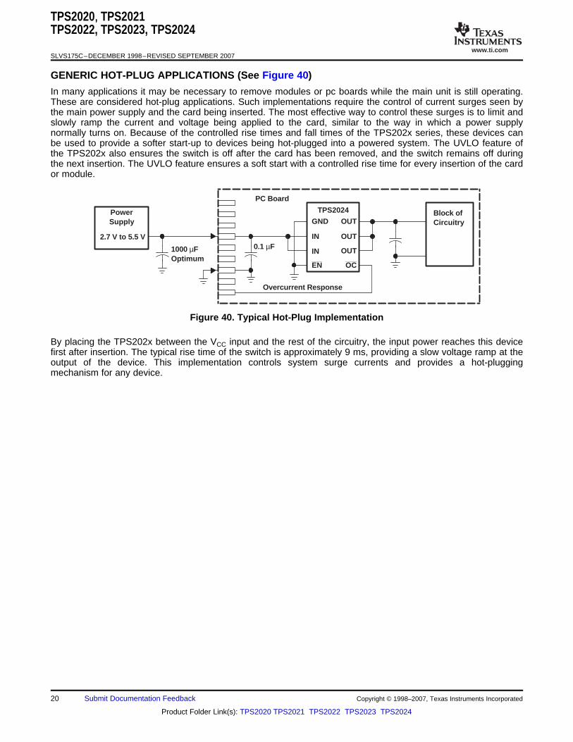
GENERIC HOT-PLUG APPLICATIONS (See Figure 40)
PowerSupply
Block ofCircuitry
TPS2024
GND
IN
IN
EN
OUT
OUT
OUT
OC
0.1 µF1000 µFOptimum
2.7 V to 5.5 V
PC Board
Overcurrent Response
TPS2020,, TPS2021TPS2022, TPS2023, TPS2024
SLVS175C–DECEMBER 1998–REVISED SEPTEMBER 2007
In many applications it may be necessary to remove modules or pc boards while the main unit is still operating.These are considered hot-plug applications. Such implementations require the control of current surges seen bythe main power supply and the card being inserted. The most effective way to control these surges is to limit andslowly ramp the current and voltage being applied to the card, similar to the way in which a power supplynormally turns on. Because of the controlled rise times and fall times of the TPS202x series, these devices canbe used to provide a softer start-up to devices being hot-plugged into a powered system. The UVLO feature ofthe TPS202x also ensures the switch is off after the card has been removed, and the switch remains off duringthe next insertion. The UVLO feature ensures a soft start with a controlled rise time for every insertion of the cardor module.
Figure 40. Typical Hot-Plug Implementation
By placing the TPS202x between the VCC input and the rest of the circuitry, the input power reaches this devicefirst after insertion. The typical rise time of the switch is approximately 9 ms, providing a slow voltage ramp at theoutput of the device. This implementation controls system surge currents and provides a hot-pluggingmechanism for any device.
20 Submit Documentation Feedback Copyright © 1998–2007, Texas Instruments Incorporated
Product Folder Link(s): TPS2020 TPS2021 TPS2022 TPS2023 TPS2024
PACKAGE OPTION ADDENDUM
www.ti.com 10-Jun-2014
Addendum-Page 1
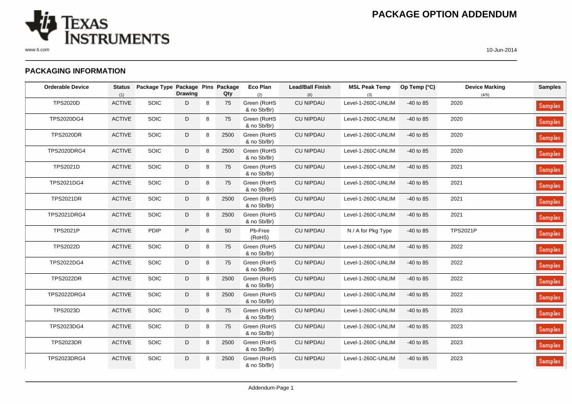
PACKAGING INFORMATION
Orderable Device Status(1)
Package Type PackageDrawing
Pins PackageQty
Eco Plan(2)
Lead/Ball Finish(6)
MSL Peak Temp(3)
Op Temp (°C) Device Marking(4/5)
Samples
TPS2020D ACTIVE SOIC D 8 75 Green (RoHS& no Sb/Br)
CU NIPDAU Level-1-260C-UNLIM -40 to 85 2020
TPS2020DG4 ACTIVE SOIC D 8 75 Green (RoHS& no Sb/Br)
CU NIPDAU Level-1-260C-UNLIM -40 to 85 2020
TPS2020DR ACTIVE SOIC D 8 2500 Green (RoHS& no Sb/Br)
CU NIPDAU Level-1-260C-UNLIM -40 to 85 2020
TPS2020DRG4 ACTIVE SOIC D 8 2500 Green (RoHS& no Sb/Br)
CU NIPDAU Level-1-260C-UNLIM -40 to 85 2020
TPS2021D ACTIVE SOIC D 8 75 Green (RoHS& no Sb/Br)
CU NIPDAU Level-1-260C-UNLIM -40 to 85 2021
TPS2021DG4 ACTIVE SOIC D 8 75 Green (RoHS& no Sb/Br)
CU NIPDAU Level-1-260C-UNLIM -40 to 85 2021
TPS2021DR ACTIVE SOIC D 8 2500 Green (RoHS& no Sb/Br)
CU NIPDAU Level-1-260C-UNLIM -40 to 85 2021
TPS2021DRG4 ACTIVE SOIC D 8 2500 Green (RoHS& no Sb/Br)
CU NIPDAU Level-1-260C-UNLIM -40 to 85 2021
TPS2021P ACTIVE PDIP P 8 50 Pb-Free(RoHS)
CU NIPDAU N / A for Pkg Type -40 to 85 TPS2021P
TPS2022D ACTIVE SOIC D 8 75 Green (RoHS& no Sb/Br)
CU NIPDAU Level-1-260C-UNLIM -40 to 85 2022
TPS2022DG4 ACTIVE SOIC D 8 75 Green (RoHS& no Sb/Br)
CU NIPDAU Level-1-260C-UNLIM -40 to 85 2022
TPS2022DR ACTIVE SOIC D 8 2500 Green (RoHS& no Sb/Br)
CU NIPDAU Level-1-260C-UNLIM -40 to 85 2022
TPS2022DRG4 ACTIVE SOIC D 8 2500 Green (RoHS& no Sb/Br)
CU NIPDAU Level-1-260C-UNLIM -40 to 85 2022
TPS2023D ACTIVE SOIC D 8 75 Green (RoHS& no Sb/Br)
CU NIPDAU Level-1-260C-UNLIM -40 to 85 2023
TPS2023DG4 ACTIVE SOIC D 8 75 Green (RoHS& no Sb/Br)
CU NIPDAU Level-1-260C-UNLIM -40 to 85 2023
TPS2023DR ACTIVE SOIC D 8 2500 Green (RoHS& no Sb/Br)
CU NIPDAU Level-1-260C-UNLIM -40 to 85 2023
TPS2023DRG4 ACTIVE SOIC D 8 2500 Green (RoHS& no Sb/Br)
CU NIPDAU Level-1-260C-UNLIM -40 to 85 2023

PACKAGE OPTION ADDENDUM
www.ti.com 10-Jun-2014
Addendum-Page 2
Orderable Device Status(1)
Package Type PackageDrawing
Pins PackageQty
Eco Plan(2)
Lead/Ball Finish(6)
MSL Peak Temp(3)
Op Temp (°C) Device Marking(4/5)
Samples
TPS2023P ACTIVE PDIP P 8 50 Pb-Free(RoHS)
CU NIPDAU N / A for Pkg Type -40 to 85 TPS2023P
TPS2024D ACTIVE SOIC D 8 75 Green (RoHS& no Sb/Br)
CU NIPDAU Level-1-260C-UNLIM -40 to 85 2024
TPS2024DG4 ACTIVE SOIC D 8 75 Green (RoHS& no Sb/Br)
CU NIPDAU Level-1-260C-UNLIM -40 to 85 2024
TPS2024DR ACTIVE SOIC D 8 2500 Green (RoHS& no Sb/Br)
CU NIPDAU Level-1-260C-UNLIM -40 to 85 2024
TPS2024DRG4 ACTIVE SOIC D 8 2500 Green (RoHS& no Sb/Br)
CU NIPDAU Level-1-260C-UNLIM -40 to 85 2024
TPS2024P ACTIVE PDIP P 8 50 Pb-Free(RoHS)
CU NIPDAU N / A for Pkg Type -40 to 85 TPS2024P
(1) The marketing status values are defined as follows:ACTIVE: Product device recommended for new designs.LIFEBUY: TI has announced that the device will be discontinued, and a lifetime-buy period is in effect.NRND: Not recommended for new designs. Device is in production to support existing customers, but TI does not recommend using this part in a new design.PREVIEW: Device has been announced but is not in production. Samples may or may not be available.OBSOLETE: TI has discontinued the production of the device.
(2) Eco Plan - The planned eco-friendly classification: Pb-Free (RoHS), Pb-Free (RoHS Exempt), or Green (RoHS & no Sb/Br) - please check http://www.ti.com/productcontent for the latest availabilityinformation and additional product content details.TBD: The Pb-Free/Green conversion plan has not been defined.Pb-Free (RoHS): TI's terms "Lead-Free" or "Pb-Free" mean semiconductor products that are compatible with the current RoHS requirements for all 6 substances, including the requirement thatlead not exceed 0.1% by weight in homogeneous materials. Where designed to be soldered at high temperatures, TI Pb-Free products are suitable for use in specified lead-free processes.Pb-Free (RoHS Exempt): This component has a RoHS exemption for either 1) lead-based flip-chip solder bumps used between the die and package, or 2) lead-based die adhesive used betweenthe die and leadframe. The component is otherwise considered Pb-Free (RoHS compatible) as defined above.Green (RoHS & no Sb/Br): TI defines "Green" to mean Pb-Free (RoHS compatible), and free of Bromine (Br) and Antimony (Sb) based flame retardants (Br or Sb do not exceed 0.1% by weightin homogeneous material)
(3) MSL, Peak Temp. - The Moisture Sensitivity Level rating according to the JEDEC industry standard classifications, and peak solder temperature.
(4) There may be additional marking, which relates to the logo, the lot trace code information, or the environmental category on the device.
(5) Multiple Device Markings will be inside parentheses. Only one Device Marking contained in parentheses and separated by a "~" will appear on a device. If a line is indented then it is a continuationof the previous line and the two combined represent the entire Device Marking for that device.
PACKAGE OPTION ADDENDUM
www.ti.com 10-Jun-2014
Addendum-Page 3
(6) Lead/Ball Finish - Orderable Devices may have multiple material finish options. Finish options are separated by a vertical ruled line. Lead/Ball Finish values may wrap to two lines if the finishvalue exceeds the maximum column width.
Important Information and Disclaimer:The information provided on this page represents TI's knowledge and belief as of the date that it is provided. TI bases its knowledge and belief on informationprovided by third parties, and makes no representation or warranty as to the accuracy of such information. Efforts are underway to better integrate information from third parties. TI has taken andcontinues to take reasonable steps to provide representative and accurate information but may not have conducted destructive testing or chemical analysis on incoming materials and chemicals.TI and TI suppliers consider certain information to be proprietary, and thus CAS numbers and other limited information may not be available for release.
In no event shall TI's liability arising out of such information exceed the total purchase price of the TI part(s) at issue in this document sold by TI to Customer on an annual basis.
OTHER QUALIFIED VERSIONS OF TPS2020, TPS2021, TPS2022, TPS2024 :
• Automotive: TPS2020-Q1, TPS2021-Q1, TPS2022-Q1, TPS2024-Q1
NOTE: Qualified Version Definitions:
• Automotive - Q100 devices qualified for high-reliability automotive applications targeting zero defects
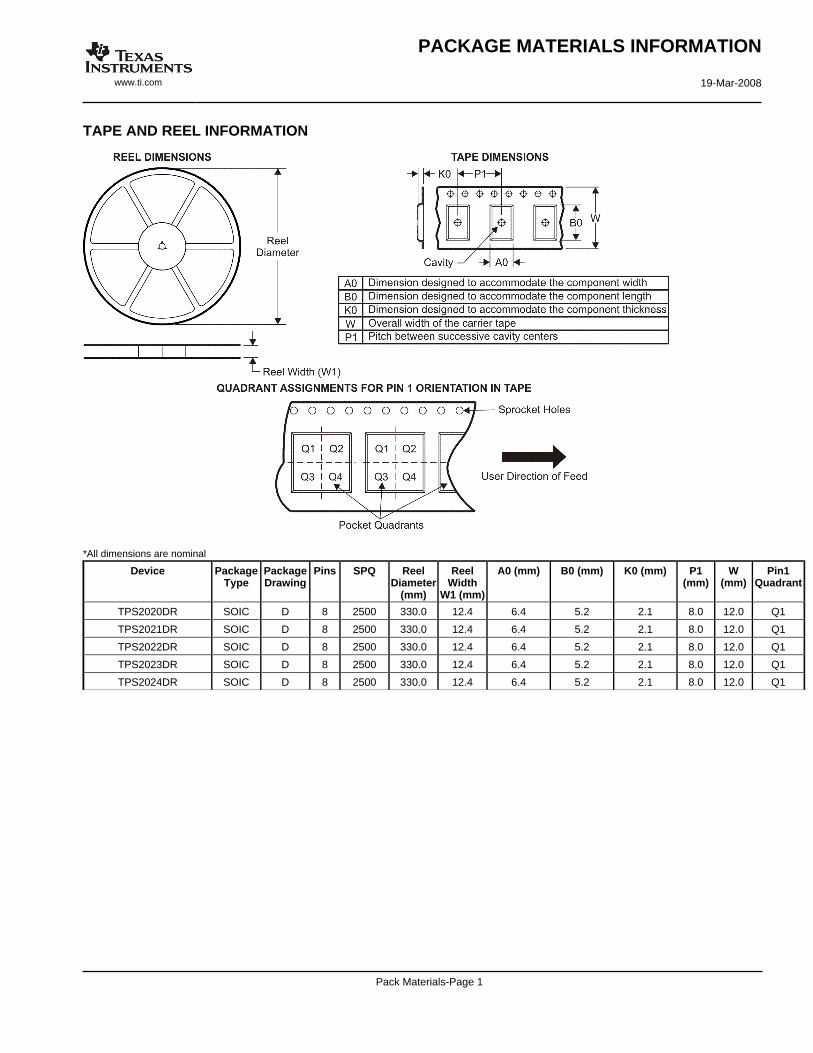
TAPE AND REEL INFORMATION
*All dimensions are nominal
Device PackageType
PackageDrawing
Pins SPQ ReelDiameter
(mm)
ReelWidth
W1 (mm)
A0 (mm) B0 (mm) K0 (mm) P1(mm)
W(mm)
Pin1Quadrant
TPS2020DR SOIC D 8 2500 330.0 12.4 6.4 5.2 2.1 8.0 12.0 Q1
TPS2021DR SOIC D 8 2500 330.0 12.4 6.4 5.2 2.1 8.0 12.0 Q1
TPS2022DR SOIC D 8 2500 330.0 12.4 6.4 5.2 2.1 8.0 12.0 Q1
TPS2023DR SOIC D 8 2500 330.0 12.4 6.4 5.2 2.1 8.0 12.0 Q1
TPS2024DR SOIC D 8 2500 330.0 12.4 6.4 5.2 2.1 8.0 12.0 Q1
PACKAGE MATERIALS INFORMATION
www.ti.com 19-Mar-2008
Pack Materials-Page 1

*All dimensions are nominal
Device Package Type Package Drawing Pins SPQ Length (mm) Width (mm) Height (mm)
TPS2020DR SOIC D 8 2500 340.5 338.1 20.6
TPS2021DR SOIC D 8 2500 340.5 338.1 20.6
TPS2022DR SOIC D 8 2500 340.5 338.1 20.6
TPS2023DR SOIC D 8 2500 340.5 338.1 20.6
TPS2024DR SOIC D 8 2500 340.5 338.1 20.6
PACKAGE MATERIALS INFORMATION
www.ti.com 19-Mar-2008
Pack Materials-Page 2
IMPORTANT NOTICE
Texas Instruments Incorporated and its subsidiaries (TI) reserve the right to make corrections, enhancements, improvements and otherchanges to its semiconductor products and services per JESD46, latest issue, and to discontinue any product or service per JESD48, latestissue. Buyers should obtain the latest relevant information before placing orders and should verify that such information is current andcomplete. All semiconductor products (also referred to herein as “components”) are sold subject to TI’s terms and conditions of salesupplied at the time of order acknowledgment.TI warrants performance of its components to the specifications applicable at the time of sale, in accordance with the warranty in TI’s termsand conditions of sale of semiconductor products. Testing and other quality control techniques are used to the extent TI deems necessaryto support this warranty. Except where mandated by applicable law, testing of all parameters of each component is not necessarilyperformed.TI assumes no liability for applications assistance or the design of Buyers’ products. Buyers are responsible for their products andapplications using TI components. To minimize the risks associated with Buyers’ products and applications, Buyers should provideadequate design and operating safeguards.TI does not warrant or represent that any license, either express or implied, is granted under any patent right, copyright, mask work right, orother intellectual property right relating to any combination, machine, or process in which TI components or services are used. Informationpublished by TI regarding third-party products or services does not constitute a license to use such products or services or a warranty orendorsement thereof. Use of such information may require a license from a third party under the patents or other intellectual property of thethird party, or a license from TI under the patents or other intellectual property of TI.Reproduction of significant portions of TI information in TI data books or data sheets is permissible only if reproduction is without alterationand is accompanied by all associated warranties, conditions, limitations, and notices. TI is not responsible or liable for such altereddocumentation. Information of third parties may be subject to additional restrictions.Resale of TI components or services with statements different from or beyond the parameters stated by TI for that component or servicevoids all express and any implied warranties for the associated TI component or service and is an unfair and deceptive business practice.TI is not responsible or liable for any such statements.Buyer acknowledges and agrees that it is solely responsible for compliance with all legal, regulatory and safety-related requirementsconcerning its products, and any use of TI components in its applications, notwithstanding any applications-related information or supportthat may be provided by TI. Buyer represents and agrees that it has all the necessary expertise to create and implement safeguards whichanticipate dangerous consequences of failures, monitor failures and their consequences, lessen the likelihood of failures that might causeharm and take appropriate remedial actions. Buyer will fully indemnify TI and its representatives against any damages arising out of the useof any TI components in safety-critical applications.In some cases, TI components may be promoted specifically to facilitate safety-related applications. With such components, TI’s goal is tohelp enable customers to design and create their own end-product solutions that meet applicable functional safety standards andrequirements. Nonetheless, such components are subject to these terms.No TI components are authorized for use in FDA Class III (or similar life-critical medical equipment) unless authorized officers of the partieshave executed a special agreement specifically governing such use.Only those TI components which TI has specifically designated as military grade or “enhanced plastic” are designed and intended for use inmilitary/aerospace applications or environments. Buyer acknowledges and agrees that any military or aerospace use of TI componentswhich have not been so designated is solely at the Buyer's risk, and that Buyer is solely responsible for compliance with all legal andregulatory requirements in connection with such use.TI has specifically designated certain components as meeting ISO/TS16949 requirements, mainly for automotive use. In any case of use ofnon-designated products, TI will not be responsible for any failure to meet ISO/TS16949.
Products ApplicationsAudio www.ti.com/audio Automotive and Transportation www.ti.com/automotiveAmplifiers amplifier.ti.com Communications and Telecom www.ti.com/communicationsData Converters dataconverter.ti.com Computers and Peripherals www.ti.com/computersDLP® Products www.dlp.com Consumer Electronics www.ti.com/consumer-appsDSP dsp.ti.com Energy and Lighting www.ti.com/energyClocks and Timers www.ti.com/clocks Industrial www.ti.com/industrialInterface interface.ti.com Medical www.ti.com/medicalLogic logic.ti.com Security www.ti.com/securityPower Mgmt power.ti.com Space, Avionics and Defense www.ti.com/space-avionics-defenseMicrocontrollers microcontroller.ti.com Video and Imaging www.ti.com/videoRFID www.ti-rfid.comOMAP Applications Processors www.ti.com/omap TI E2E Community e2e.ti.comWireless Connectivity www.ti.com/wirelessconnectivity
Mailing Address: Texas Instruments, Post Office Box 655303, Dallas, Texas 75265Copyright © 2016, Texas Instruments Incorporated