tpa2005d1-q1 1.4-w mono filter-free class-d audio power
TRANSCRIPT

_
+
IN–
IN+
PWM H–
Bridge
VO+
VO–
Internal
Oscillator CS
To BatteryVDD
GND
Bias
Circuitry
RI
RI
+
–
Differential
Input
TPA2005D1
SHUTDOWN
Product
Folder
Sample &Buy
Technical
Documents
Tools &
Software
Support &Community
TPA2005D1-Q1SLOS474D –AUGUST 2005–REVISED DECEMBER 2015
TPA2005D1-Q1 1.4-W Mono Filter-Free Class-D Audio Power Amplifier1 Features 3 Description
The TPA2005D1-Q1 is a 1.4-W high-efficiency filter-1• Qualified for Automotive Applications
free class-D audio power amplifier in a SON or• AEC-Q100 Qualified With the Following Results: MSOP package that requires only three external– Device Temperature Grade 3 (DRB and DGN components.
package non T-suffix): -40°C to 85°C Ambient Features like 84% efficiency, –71-dB PSRR atOperating Temperature Range 217 Hz, improved RF-rectification immunity, and 15-– Device Temperature Grade 2 (DGN package mm2 total PCB area make TPA2005D1-Q1 ideal for
T-suffix): -40°C to 105°C Ambient Operating low-power audio applications in infotainment andcluster.Temperature Range
– Device HBM Classification Level 2 The device allows for independent gain control bysumming the signals from each function while– Device CDM Classification Level C5minimizing noise to only 48µVRMS. Additionally, the• 1.4 W Into 8 Ω From a 5-V Supply atTPA2005D1-Q1 offers fast start-up time of 9ms withTHD = 10% (Typ) minimal pop and has short circuit and thermal
• Maximum Battery Life and Minimum Heat protection.– Efficiency With an 8-Ω Speaker:
Device Information(1)– 84% at 400 mW
PART NUMBER PACKAGE BODY SIZE (NOM)– 79% at 100 mWMSOP-PowerPAD (8) 3.00 mm × 3.00 mm
TPA2005D1-Q1– 2.8-mA Quiescent CurrentSON (8) 3.00 mm × 3.00 mm
– 0.5-μA Shutdown Current(1) For all available packages, see the orderable addendum at• Only Three External Components the end of the datasheet.
– Optimized PWM Output Stage Eliminates LCApplication CircuitOutput Filter
– Internally Generated 250-kHz SwitchingFrequency Eliminates Capacitor and Resistor
– Improved PSRR (–71 dB at 217 Hz) and WideSupply Voltage (2.5 V to 5.5 V) EliminatesNeed for a Voltage Regulator
– Fully Differential Design Reduces RFRectification and Eliminates Bypass Capacitor
– Improved CMRR Eliminates Two InputCoupling Capacitors
• Space-Saving Packages– 3 mm x 3 mm SON package (DRB)– 3 mm x 5 mm MSOP PowerPAD™ Package
(DGN)
2 Applications• Cluster• Head Unit• Telematics• Emergency Call (eCall)• Noise Generator
1
An IMPORTANT NOTICE at the end of this data sheet addresses availability, warranty, changes, use in safety-critical applications,intellectual property matters and other important disclaimers. PRODUCTION DATA.

TPA2005D1-Q1SLOS474D –AUGUST 2005–REVISED DECEMBER 2015 www.ti.com
Table of Contents9.2 Functional Block Diagram ....................................... 121 Features .................................................................. 19.3 Feature Description................................................. 122 Applications ........................................................... 19.4 Device Functional Modes........................................ 163 Description ............................................................. 1
10 Application and Implementation........................ 194 Revision History..................................................... 210.1 Application Information.......................................... 195 Device Comparison Table ..................................... 310.2 Typical Application ................................................ 196 Pin Configuration and Functions ......................... 3
11 Power Supply Recommendations ..................... 237 Specifications......................................................... 411.1 Power Supply Decoupling Capacitors................... 237.1 Absolute Maximum Ratings ...................................... 4
12 Layout................................................................... 247.2 ESD Ratings.............................................................. 412.1 Layout Guidelines ................................................. 247.3 Recommended Operating Conditions....................... 412.2 Layout Example .................................................... 257.4 Thermal Information .................................................. 4
13 Device and Documentation Support ................. 267.5 Electrical Characteristics........................................... 513.1 Community Resource............................................ 267.6 Operating Characteristics.......................................... 513.2 Trademarks ........................................................... 267.7 Typical Characteristics .............................................. 613.3 Electrostatic Discharge Caution............................ 268 Parameter Measurement Information ................ 1113.4 Glossary ................................................................ 269 Detailed Description ............................................ 12
14 Mechanical, Packaging, and Orderable9.1 Overview ................................................................. 12 Information ........................................................... 26
4 Revision HistoryNOTE: Page numbers for previous revisions may differ from page numbers in the current version.
Changes from Revision C (March 2010) to Revision D Page
• Added Applications, ESD Rating table, Feature Description section, Device Functional Modes, Application andImplementation section, Power Supply Recommendations section, Layout section, Device and DocumentationSupport section, and Mechanical, Packaging, and Orderable Information section. .............................................................. 1
• Deleted Ordering Information table. See POA in the back of document. .............................................................................. 1• Added RL Load resistance, to the Abs Max Ratings Table .................................................................................................... 4• Changed Storage temperature From: -65°C to 85°C To: -65°C to 150°C ............................................................................. 4• Deleted Dissipation Ratings table and added Thermal Information table. ............................................................................ 4• Updated Efficiency and Thermal Information ...................................................................................................................... 13
2 Submit Documentation Feedback Copyright © 2005–2015, Texas Instruments Incorporated
Product Folder Links: TPA2005D1-Q1

8SHUTDOWN
NC
IN+
IN−
VO−
GND
VDD
VO+
8-PIN QFN (DRB) PACKAGE
(TOP VIEW)
7
6
5
1
2
3
4
NC − No internal connection
VO−
GND
VDD
VO+
8
7
6
5
1
2
3
4
SHUTDOWN
NC
IN+
IN−
8-PIN MSOP (DGN) PACKAGE
(TOP VIEW)
TPA2005D1-Q1www.ti.com SLOS474D –AUGUST 2005–REVISED DECEMBER 2015
5 Device Comparison Table
DEVICE SPEAKER SPEAKER AMP OUTPUT POWER PSRR (dB) SUPPLY MIN (V) SUPPLY MAX (V) PACKAGENUMBER CHANNELS TYPE (W) FAMILY
MSOP-PowerPADTPA2005D1-Q1 Mono Class D 1.4 75 2.5 5.5
SON
TPA2000D1-Q1 Mono Class D 2 77 2.7 5.5 TSSOP
6 Pin Configuration and Functions
A. The shaded terminals are used for electrical and thermal connections to the ground plane. All of the shaded terminalsmust be electrically connected to ground. No connect (NC) terminals still need a pad and trace.
B. The thermal pad of the DRB and DGN packages must be electrically and thermally connected to a ground plane.
Pin FunctionsPIN
I/O DESCRIPTIONNAME NO.
IN– 4 I Negative differential inputIN+ 3 I Positive differential inputVDD 6 I Power supplyVO+ 5 O Positive BTL outputGND 7 I High-current groundVO– 8 O Negative BTL outputSHUTDOWN 1 I Shutdown terminal (active low logic)NC 2 No internal connectionThermal Pad Must be soldered to a grounded pad on the PCB.
Copyright © 2005–2015, Texas Instruments Incorporated Submit Documentation Feedback 3
Product Folder Links: TPA2005D1-Q1

TPA2005D1-Q1SLOS474D –AUGUST 2005–REVISED DECEMBER 2015 www.ti.com
7 Specifications
7.1 Absolute Maximum Ratingsover operating free-air temperature range (unless otherwise noted) (1)
MIN MAX UNITIn active mode –0.3 6 V
VDD Supply voltage (2)In SHUTDOWN mode –0.3 7 V
VI Input voltage –0.3 VDD + 0.3 V VNon T-suffix –40 85Operating free-airTA °Ctemperature T-suffix –40 105
TJ Operating junction temperature –40 150 °C2.5 ≤ VDD ≤ 4.2 V 3.2 (Minimum) Ω
RL Load resistance4.2 < VDD ≤ 6 V 6.4 (Minimum) Ω
Tstg Storage temperature –65 150 °C
(1) Stresses beyond those listed under Absolute Maximum Ratings may cause permanent damage to the device. These are stress ratingsonly, which do not imply functional operation of the device at these or any other conditions beyond those indicated under RecommendedOperating Conditions. Exposure to absolute-maximum-rated conditions for extended periods may affect device reliability.
(2) For the MSOP (DGN) package option, the maximum VDD should be limited to 5 V if short-circuit protection is desired.
7.2 ESD RatingsVALUE UNIT
Human-body model (HBM), per AEC Q100-002 (1) ±2000V(ESD) Electrostatic discharge V
Charged-device model (CDM), per AEC Q100-011 ±1000
(1) AEC Q100-002 indicates that HBM stressing shall be in accordance with the ANSI/ESDA/JEDEC JS-001 specification.
7.3 Recommended Operating ConditionsMIN MAX UNIT
VDD Supply voltage 2.5 5.5 VVIH High-level input voltage SHUTDOWN 2 VDD VVIL Low-level input voltage SHUTDOWN 0 0.7 VRI Input resistor Gain ≤ 20 V/V (26 dB) 15 kΩVIC Common-mode input voltage range VDD = 2.5 V, 5.5 V, CMRR ≤ –49 dB 0.5 VDD – 0.8 V
Non T-suffix –40 85TA Operating free-air temperature °C
T-suffix –40 105
7.4 Thermal InformationTPA2005D1-Q1
DRB (SON) DGNTHERMAL METRIC (1) (MSOP UNIT
PowerPAD)8 PINS 8 PINS
RθJA Junction-to-ambient thermal resistance 49.5 57 °C/WRθJC(top) Junction-to-case (top) thermal resistance 62.1 53.8 °C/WRθJB Junction-to-board thermal resistance 24.8 33.7 °C/WψJT Junction-to-top characterization parameter 1.3 1.9 °C/WψJB Junction-to-board characterization parameter 24.9 33.4 °C/WRθJC(bot) Junction-to-case (bottom) thermal resistance 6.9 6.4 °C/W
(1) For more information about traditional and new thermal metrics, see the Semiconductor and IC Package Thermal Metrics applicationreport, SPRA953.
4 Submit Documentation Feedback Copyright © 2005–2015, Texas Instruments Incorporated
Product Folder Links: TPA2005D1-Q1
2 150 kRI
2 142 kRI
2 158 kRI
VV
TPA2005D1-Q1www.ti.com SLOS474D –AUGUST 2005–REVISED DECEMBER 2015
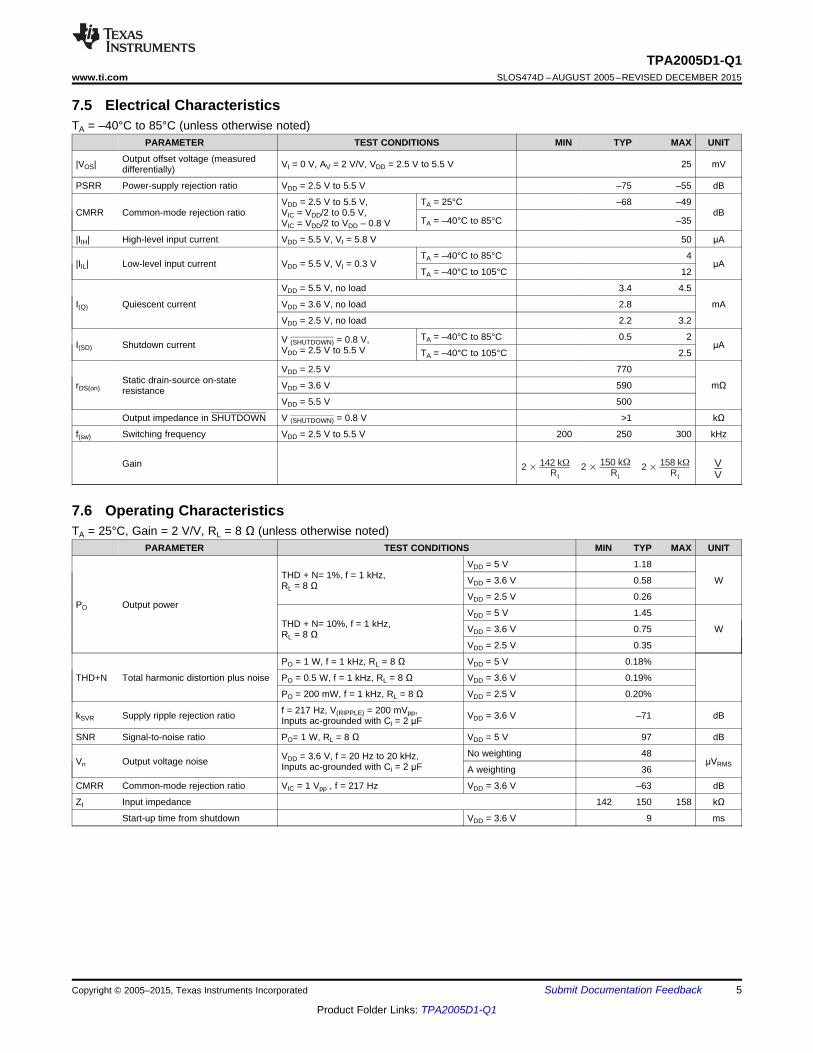
7.5 Electrical CharacteristicsTA = –40°C to 85°C (unless otherwise noted)
PARAMETER TEST CONDITIONS MIN TYP MAX UNIT
Output offset voltage (measured|VOS| VI = 0 V, AV = 2 V/V, VDD = 2.5 V to 5.5 V 25 mVdifferentially)
PSRR Power-supply rejection ratio VDD = 2.5 V to 5.5 V –75 –55 dB
VDD = 2.5 V to 5.5 V, TA = 25°C –68 –49CMRR Common-mode rejection ratio VIC = VDD/2 to 0.5 V, dB
TA = –40°C to 85°C –35VIC = VDD/2 to VDD – 0.8 V
|IIH| High-level input current VDD = 5.5 V, VI = 5.8 V 50 μA
TA = –40°C to 85°C 4|IIL| Low-level input current VDD = 5.5 V, VI = 0.3 V μA
TA = –40°C to 105°C 12
VDD = 5.5 V, no load 3.4 4.5
I(Q) Quiescent current VDD = 3.6 V, no load 2.8 mA
VDD = 2.5 V, no load 2.2 3.2
TA = –40°C to 85°C 0.5 2V (SHUTDOWN) = 0.8 V,I(SD) Shutdown current μAVDD = 2.5 V to 5.5 V TA = –40°C to 105°C 2.5
VDD = 2.5 V 770Static drain-source on-staterDS(on) VDD = 3.6 V 590 mΩresistance
VDD = 5.5 V 500
Output impedance in SHUTDOWN V (SHUTDOWN) = 0.8 V >1 kΩ
f(sw) Switching frequency VDD = 2.5 V to 5.5 V 200 250 300 kHz
Gain
7.6 Operating CharacteristicsTA = 25°C, Gain = 2 V/V, RL = 8 Ω (unless otherwise noted)
PARAMETER TEST CONDITIONS MIN TYP MAX UNIT
VDD = 5 V 1.18THD + N= 1%, f = 1 kHz, VDD = 3.6 V 0.58 WRL = 8 Ω
VDD = 2.5 V 0.26PO Output power
VDD = 5 V 1.45THD + N= 10%, f = 1 kHz, VDD = 3.6 V 0.75 WRL = 8 Ω
VDD = 2.5 V 0.35
PO = 1 W, f = 1 kHz, RL = 8 Ω VDD = 5 V 0.18%
THD+N Total harmonic distortion plus noise PO = 0.5 W, f = 1 kHz, RL = 8 Ω VDD = 3.6 V 0.19%
PO = 200 mW, f = 1 kHz, RL = 8 Ω VDD = 2.5 V 0.20%
f = 217 Hz, V(RIPPLE) = 200 mVpp,kSVR Supply ripple rejection ratio VDD = 3.6 V –71 dBInputs ac-grounded with Ci = 2 μF
SNR Signal-to-noise ratio PO= 1 W, RL = 8 Ω VDD = 5 V 97 dB
No weighting 48VDD = 3.6 V, f = 20 Hz to 20 kHz,Vn Output voltage noise μVRMSInputs ac-grounded with Ci = 2 μF A weighting 36
CMRR Common-mode rejection ratio VIC = 1 Vpp , f = 217 Hz VDD = 3.6 V –63 dB
ZI Input impedance 142 150 158 kΩ
Start-up time from shutdown VDD = 3.6 V 9 ms
Copyright © 2005–2015, Texas Instruments Incorporated Submit Documentation Feedback 5
Product Folder Links: TPA2005D1-Q1
0
50
100
150
200
250
0 0.1 0.2 0.3 0.4 0.5 0.6
RL = 8 W, 33 Hm
VDD = 3.6 V
RL = 32 W, 33 Hm
Su
pp
ly C
urr
en
t -
mA
PO - Output Power - W
0
50
100
150
200
250
300
0 0.2 0.4 0.6 0.8 1 1.2
PO - Output Power - W
VDD = 2.5 V,
RL = 8 W, 33 Hm
VDD = 3.6 V,
RL = 8 W, 33 Hm
VDD = 5 V,
RL = 8 W, 33 Hm
Su
pp
ly C
urr
en
t -
mA
0 0.5 1 1.5
P - Output Power - WO
0
10
20
30
40
50
60
70
80
90
Eff
icie
ncy -
%
V = 4.2 V,DD
R = 4 , 33 HL W m
0
0.1
0.2
0.3
0.4
0.5
0.6
0.7
0 0.2 0.4 0.6 0.8 1 1.2
- P
ow
er
Dis
sip
ation -
WPD
PO - Output Power - W
Class-AB, VDD = 5 V, RL = 8 W
Class-AB,
VDD = 3.6 V,
RL = 8 W
VDD = 3.6 V,
RL = 8 W, 33 mH
VDD = 5 V,
RL = 8 W, 33 mH
V = 4.2 V,
R = 4 , 33 Hm
DD
L W
0
10
20
30
40
50
60
70
80
90
100
0 0.1 0.2 0.3 0.4 0.5 0.6
PO - Output Power - W
Eff
icie
nc
y -
%
VDD = 3.6
R = 32 , 33 HL W m
R = 16 , 33 HL W m
R = 8 , 33 HL W m
Class-AB,
RL = 8 Ω
0
10
20
30
40
50
60
70
80
90
0 0.2 0.4 0.6 0.8 1 1.2
V = 5 V,DD
R = 8 , 33 HL W mV = 2.5 V,DD
R = 8 , 33 HL W m
Class-AB,
DD = 5 V,
RL = 8 W
V
PO - Output Power - W
Effic
ien
cy -
%
TPA2005D1-Q1SLOS474D –AUGUST 2005–REVISED DECEMBER 2015 www.ti.com
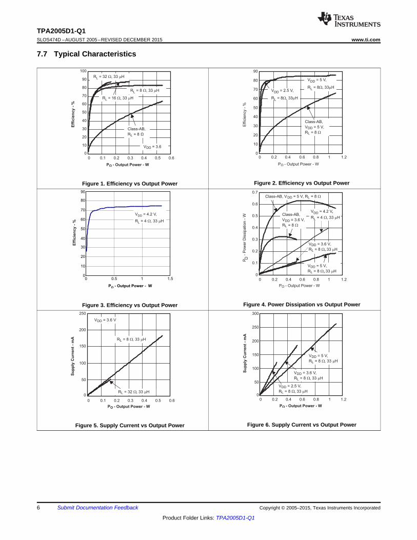
7.7 Typical Characteristics
Figure 2. Efficiency vs Output PowerFigure 1. Efficiency vs Output Power
Figure 4. Power Dissipation vs Output PowerFigure 3. Efficiency vs Output Power
Figure 6. Supply Current vs Output PowerFigure 5. Supply Current vs Output Power
6 Submit Documentation Feedback Copyright © 2005–2015, Texas Instruments Incorporated
Product Folder Links: TPA2005D1-Q1

0
0.2
0.4
0.6
0.8
1
1.2
1.4
4 8 12 16 20 24 28 32
R - Load Resistance -L W
V = 4.2 VDD
V = 3.6 VDD
V = 2.5 VDD
V = 5 VDD
f = 1 kHz,THD+N = 1%,Gain = 2 V/V
P-
Outp
ut P
ow
er
- W
O
0
0.2
0.4
0.6
0.8
1
1.2
1.4
1.6
1.8
4 8 12 16 20 24 28 32
R - Load Resistance -L W
V = 4.2 VDD
V = 3.6 VDD
V = 2.5 VDD
V = 5 VDD
P-
Outp
ut P
ow
er
- W
O
f = 1 kHz,THD+N = 10%,Gain = 2 V/V
0
0.2
0.4
0.6
0.8
1
1.2
1.4
1.6
2.5 3 3.5 4 4.5
V - Supply Voltage - VDD
P-
Ou
tpu
t P
ow
er
- W
O
THD+N = 10%
THD+N = 1%
R = 4 ,L W
f = 1kHz,
Gain = 2 V/V
2.5 3 3.5 4 4.5 5
VDD - Supply Voltage - V
- O
utp
ut
Po
wer
- W
PO
RL = 8 W
f = 1 kHz
Gain = 2 V/V
THD+N = 1%
THD+N = 10%
0
0.2
0.4
0.6
0.8
1
1.2
1.4
1.6
2
2.2
2.4
2.6
2.8
3
3.2
3.4
3.6
3.8
2.5 3 3.5 4 4.5 5 5.5
I (Q
)−
Qu
iescen
t C
urr
en
t−
mA
VDD − Supply Voltage − V
No Load
RL = 8 W, 33 Hm
0
0.1
0.2
0.3
0.4
0.5
0.6
0.7
0.8
0.9
1
0 0.1 0.2 0.3 0.4 0.5 0.6 0.7 0.8
VDD = 2.5 V
VDD = 3.6 V
VDD = 5 V
Shutdown Voltage - V
- S
hu
tdo
wn
Cu
rren
t -
I (S
D)
Am
TPA2005D1-Q1www.ti.com SLOS474D –AUGUST 2005–REVISED DECEMBER 2015
Typical Characteristics (continued)
Figure 7. Quiescent Current vs Supply Voltage Figure 8. Shutdown Current vs Shutdown Voltage
Figure 9. Output Power vs Supply Voltage Figure 10. Output Power vs Supply Voltage
Figure 12. Output Power vs Load ResistanceFigure 11. Output Power vs Load Resistance
Copyright © 2005–2015, Texas Instruments Incorporated Submit Documentation Feedback 7
Product Folder Links: TPA2005D1-Q1

1
2
5
10
0.5
0.2
0.1
0.05
0.02
0.01
20 100 1 k 20 k
f − Frequency − Hz
TH
D+
N−
To
tal
Harm
on
ic D
isto
rtio
n +
No
ise
−%
VDD = 3.6 V
CI = 2 Fm
RL = 8 W
Gain = 2 V/V
500 mW
25 mW
125 mW
10
5
2
1
0.5
0.2
0.1
0.05
0.02
0.0120 100 1 k 20 k
f − Frequency − Hz
TH
D+
N−
To
tal
Harm
on
ic D
isto
rtio
n +
No
ise
−%
15 mW
VDD = 2.5 V
CI = 2 Fm
RL = 8 W
Gain = 2 V/V
75 mW
200 mW
0.1
30
0.2
0.5
1
2
5
10
20
0.01 20.1 1
PO − Output Power − W
TH
D+
N−
To
tal
Harm
on
ic D
isto
rtio
n +
No
ise
−%
5 V
3.6 V
2.5 V
RL = 16 ,W
f = 1 kHz,
Gain = 2 V/V
0.008
10
0.02
0.05
0.1
0.2
0.5
1
2
5
20 100 1 k 20 k
f − Frequency − Hz
TH
D+
N−
To
tal H
arm
on
ic D
isto
rtio
n +
No
ise
−%
50 mW
250 mW
1 W
VDD = 5 V
CI = 2 Fm
RL = 8 W
Gain = 2 V/V
0.1
30
0.2
0.5
1
2
5
0.01 20.1 1
P - Output Power - WO
TH
D+
N -
To
tal
Ha
rmo
nic
Dis
tort
ion
+ N
ois
e -
%
20
V = 2.5 VDD
V = 3.6 VDD
V = 4.2 VDD
R = 4 ,L W
f = 1 kHz,
Gain = 2 V/V10
0.1
30
0.2
0.5
1
2
5
10
20
0.01 20.1 1
PO − Output Power − W
TH
D+
N−
To
tal H
arm
on
ic D
isto
rtio
n +
No
ise
−%
5 V
3.6 V
2.5 V
RL = 8 ,W
f = 1 kHz,
Gain = 2 V/V
TPA2005D1-Q1SLOS474D –AUGUST 2005–REVISED DECEMBER 2015 www.ti.com
Typical Characteristics (continued)
Figure 14. Total Harmonic Distortion + Noise vs OutputFigure 13. Total Harmonic Distortion + Noise vs OutputPowerPower
Figure 16. Total Harmonic Distortion + Noise vs FrequencyFigure 15. Total Harmonic Distortion + Noise vs OutputPower
Figure 17. Total Harmonic Distortion + Noise vs Frequency Figure 18. Total Harmonic Distortion + Noise vs Frequency
8 Submit Documentation Feedback Copyright © 2005–2015, Texas Instruments Incorporated
Product Folder Links: TPA2005D1-Q1

−80
−70
−60
−50
−40
−30
−20
−10
0
20 100 1 k 20 k
f − Frequency − Hz
−S
up
ply
Vo
ltag
e R
eje
cti
on
Rati
o−
dB
kS
VR
CI = 2 Fm
RL = 8 W
Vp-p = 200 mV
Inputs ac-Grounded
Gain = 2 V/V
VDD = 5 V
VDD = 3.6 V
VDD =2. 5 V
0.1
1
10
0 0.5 1 1.5 2 2.5 3 3.5
VDD = 2.5 V
VDD = 3.6 V
f = 1 kHz
PO = 200 mW
VIC - Common Mode Input Voltage - V
TH
D+
N -
To
tal
Harm
on
ic D
isto
rtio
n +
No
ise
- %
0.01
10
0.02
0.05
0.1
0.2
0.5
1
2
5
20 20k100 1kTH
D+
N -
To
tal H
arm
on
ic D
isto
rtio
n +
No
ise -
%
f-Frequency-Hz
500 mW
250 mW
775 mW
V = 3.6 V,DD
R = 4 ,L W
Gain = 2V/V
20 100
10
5
2
1
0.5
0.2
0.1
0.05
0.02
0.011k 20k
200 mW
75 mW
15 mW
V = 2.5 V,DD
R = 4 ,L W
Gain = 2V/V
f - Frequency - Hz
TH
D+
N -
To
tal
Ha
rmo
nic
Dis
tort
ion
+ N
ois
e -
%
VDD = 3.6 V
CI = 2 Fm
RL = 16 W
Gain = 2 V/V
f − Frequency − Hz
TH
D+
N−
To
tal H
arm
on
ic D
isto
rtio
n +
No
ise
−%
1
2
5
10
0.5
0.2
0.1
0.05
0.02
0.0120 100 1 k 20 k
15 mW
75 mW
200 mW0.01
10
0.02
0.05
0.1
0.2
0.5
1
2
5
20 20k100 1k
f - Frequency - Hz
TH
D+
N -
To
tal H
arm
on
ic D
isto
rtio
n +
No
ise -
%
1 W
500 mW
250 mW
V = 4.2 V,DD
R = 4 ,L W
Gain = 2 V/V
TPA2005D1-Q1www.ti.com SLOS474D –AUGUST 2005–REVISED DECEMBER 2015
Typical Characteristics (continued)
Figure 20. Total Harmonic Distortion + Noise vs FrequencyFigure 19. Total Harmonic Distortion + Noise vs Frequency
Figure 21. Total Harmonic Distortion + Noise vs Frequency Figure 22. Total Harmonic Distortion + Noise vs Frequency
Figure 23. Total Harmonic Distortion + Noise vs Figure 24. Supply Voltage Rejection Ratio vs FrequencyCommon Mode Input Voltage
Copyright © 2005–2015, Texas Instruments Incorporated Submit Documentation Feedback 9
Product Folder Links: TPA2005D1-Q1
-100
-90
-80
-70
-60
-50
-40
-30
-20
-10
0
0 0.5 1 1.5 2 2.5 3 3.5 4 4.5 5
RL = 8W
Gain = 2 V/V
VIC - Common Mode Input Voltage - V
CM
RR
- C
om
mo
n M
od
e R
eje
cti
on
Rati
o -
dB
VDD = 5 V
VDD = 2.5 V VDD = 3.6 V
−70
−60
−50
−40
−30
−20
−10
0
f − Frequency − Hz
CM
RR
−C
om
mo
n M
od
e R
eje
cti
on
Rati
o−
dB
20 100 1 k 20 k
VDD = 2.5 V to 5 V
VIC = 1 Vp−p
RL = 8 W
Gain = 2 V/V
-90
-80
-70
-60
-50
-40
-30
-20
-10
0
0 0.5 1 1.5 2 2.5 3 3.5 4 4.5 5
VIC - Common Mode Input Voltage - V
f = 217 Hz
RL = 8 W
Gain = 2 V/V
VDD = 2.5 V
- S
up
ply
Vo
ltag
e R
eje
cti
on
Rati
o -
dB
kS
VR
VDD = 3.6 V
VDD = 5 V
−80
−70
−60
−50
−40
−30
−20
−10
0
f − Frequency − Hz
−S
up
ply
Vo
ltag
e R
eje
cti
on
Rati
o−
dB
kS
VR
20 100 1 k 20 k
Gain = 5 V/V
CI = 2 Fm
RL = 8 W
Vp-p = 200 mV
Inputs ac-Grounded
VDD = 5 V
VDD = 2. 5 V
VDD = 3.6 V
−100
−90
−80
−70
−60
−50
−40
−30
−20
−10
0
f − Frequency − Hz
−S
up
ply
Vo
ltag
e R
eje
cti
on
Rati
o−
dB
kS
VR
VDD = 3.6 V
CI = 2 Fm
RL = 8 W
Inputs Floating
Gain = 2 V/V
20 100 1 k 20 k
TPA2005D1-Q1SLOS474D –AUGUST 2005–REVISED DECEMBER 2015 www.ti.com
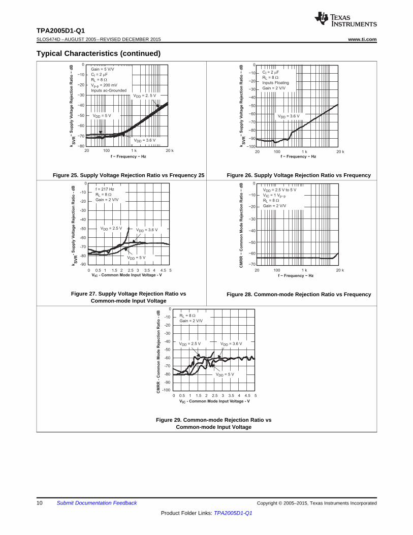
Typical Characteristics (continued)
Figure 25. Supply Voltage Rejection Ratio vs Frequency 25 Figure 26. Supply Voltage Rejection Ratio vs Frequency
Figure 27. Supply Voltage Rejection Ratio vs Figure 28. Common-mode Rejection Ratio vs FrequencyCommon-mode Input Voltage
Figure 29. Common-mode Rejection Ratio vsCommon-mode Input Voltage
10 Submit Documentation Feedback Copyright © 2005–2015, Texas Instruments Incorporated
Product Folder Links: TPA2005D1-Q1
MeasurementOutput
VDD
30 kHzLow Pass
Filter
Measurement Input
IN+ OUT+
IN± OUT±
VDD GND
+
±
+
±
LoadCI
CI
RI
RI+
±
1 mF
TPA2005D1
TPA2005D1-Q1www.ti.com SLOS474D –AUGUST 2005–REVISED DECEMBER 2015
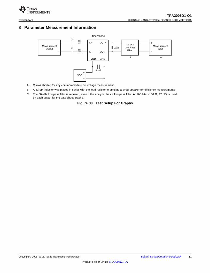
8 Parameter Measurement Information
A. CI was shorted for any common-mode input voltage measurement.B. A 33-μH inductor was placed in series with the load resistor to emulate a small speaker for efficiency measurements.C. The 30-kHz low-pass filter is required, even if the analyzer has a low-pass filter. An RC filter (100 Ω, 47 nF) is used
on each output for the data sheet graphs.
Figure 30. Test Setup For Graphs
Copyright © 2005–2015, Texas Instruments Incorporated Submit Documentation Feedback 11
Product Folder Links: TPA2005D1-Q1

_
+_+
_
+_+
150 kW
150 kW
_
+
_
+
Deglitch
Logic
Deglitch
Logic
Gate
Drive
Gate
Drive
VDD
Short
Circuit
Detect
Startup
& Thermal
Protection
Logic
Ramp
Generator
Biases
and
References
TTL
Input
Buffer
SD
Gain = 2 V/V
B4, C4VDD
A4VO−
D4VO+
GND
D1IN−
C1IN+
A1SHUTDOWN
TPA2005D1-Q1SLOS474D –AUGUST 2005–REVISED DECEMBER 2015 www.ti.com
9 Detailed Description
9.1 OverviewThe TPA2005D1-Q1 is a high-efficiency filter-free Class-D audio amplifier capable of delivering up to 1.4 W into8-Ω loads with a 5-V power supply. The fully-differential design of this amplifier avoids the usage of bypasscapacitors and the improved CMRR eliminates the usage of input-coupling capacitors. This makes the devicesize a perfect choice for small, space constrained applications as only three external components are required.The advanced modulation used in the TPA2005D1-Q1 PWM output stage eliminates the need for an output filter.
9.2 Functional Block Diagram
9.3 Feature Description
9.3.1 Fully Differential AmplifierThe TPA2005D1-Q1 is a fully differential amplifier with differential inputs and outputs. The fully differentialamplifier consists of a differential amplifier and a common-mode amplifier. The differential amplifier ensures thatthe amplifier outputs a differential voltage on the output that is equal to the differential input times the gain. Thecommon-mode feedback ensures that the common-mode voltage at the output is biased around VDD/2,regardless of the common-mode voltage at the input. The fully differential TPA2005D1-Q1 can still be used witha single-ended input; however, the TPA2005D1-Q1 should be used with differential inputs when in a noisyenvironment to ensure maximum noise rejection.
9.3.1.1 Advantages Of Fully Differential Amplifiers• Input-coupling capacitors not required:
– The fully differential amplifier allows the inputs to be biased at a voltage other than mid-supply. Forexample, if a codec has a mid-supply lower than the mid-supply of the TPA2005D1-Q1, the common-mode feedback circuit adjusts, and the TPA2005D1-Q1 outputs still is biased at mid-supply of theTPA2005D1-Q1. The inputs of the TPA2005D1-Q1 can be biased from 0.5 V to VDD – 0.8 V. If the inputsare biased outside of that range, input-coupling capacitors are required.
• Mid-supply bypass capacitor, C(BYPASS), not required:– The fully differential amplifier does not require a bypass capacitor. This is because any shift in the mid-
supply affects both positive and negative channels equally and cancels at the differential output.• Better RF immunity:
– The fully differential amplifier cancels noise from RF interference much better than the typical audioamplifier.
12 Submit Documentation Feedback Copyright © 2005–2015, Texas Instruments Incorporated
Product Folder Links: TPA2005D1-Q1

0 V
–5 V
+5 V
Current
OUT+
Differential VoltageAcross Load
OUT–
TAMax TJMax JAPDmax 150 62.5 (0.2) 137.5°C
TPA2005D1-Q1www.ti.com SLOS474D –AUGUST 2005–REVISED DECEMBER 2015
Feature Description (continued)9.3.2 Efficiency and Thermal Information
As an example, the DRB package has a θJA of 49.5°C/W, the maximum allowable junction temperature of 150°C,and the maximum internal dissipation of 0.2 W (worst case 5-V supply), the maximum ambient temperature canbe calculated with Equation 1.
(1)
Equation 1 shows that the calculated maximum ambient temperature is 140.1°C at maximum power dissipationwith a 5-V supply; however, the maximum ambient temperature of the package is limited to 85°C (note that theTPA2005D1TDGNRQ1 supports up to 105°C). Because of the efficiency of the TPA2005D1-Q1, it can beoperated under all conditions to an ambient temperature of 85°C. The TPA2005D1-Q1 is designed with thermalprotection that turns the device off when the junction temperature surpasses 150°C to prevent damage to the IC.Also, using speakers more resistive than 8 Ω dramatically increases the thermal performance by reducing theoutput current and increasing the efficiency of the amplifier.
9.3.3 Eliminating the Output Filter With the TPA2005D1-Q1This section focuses on why the user can eliminate the output filter with the TPA2005D1-Q1.
9.3.3.1 Effect On AudioThe class-D amplifier outputs a pulse-width modulated (PWM) square wave, which is the sum of the switchingwaveform and the amplified input audio signal. The human ear acts as a band-pass filter such that only thefrequencies between approximately 20 Hz and 20 kHz are passed. The switching frequency components aremuch greater than 20 kHz, so the only signal heard is the amplified input audio signal.
9.3.3.2 Traditional Class-D Modulation SchemeThe traditional class-D modulation scheme has a differential output in which each output is 180 degrees out ofphase and changes from ground to the supply voltage, VDD. Therefore, the differential pre-filtered output variesbetween positive and negative VDD, where filtered 50% duty cycle yields 0 V across the load. The traditionalclass-D modulation scheme with voltage and current waveforms is shown in Figure 31. Note that, even at anaverage of 0 V across the load (50% duty cycle), the current to the load is high, causing a high loss and thuscausing a high supply current.
Figure 31. Traditional Class-D Modulation Scheme Output Voltage and Current Waveforms Into anInductive Load With No Input
Copyright © 2005–2015, Texas Instruments Incorporated Submit Documentation Feedback 13
Product Folder Links: TPA2005D1-Q1

0 V
–5 V
+5 V
Current
OUT+
OUT–
Differential
Voltage
Across
Load
0 V
–5 V
+5 V
Current
OUT+
OUT–
Differential
Voltage
Across
Load
Output = 0 V
Output > 0 V
TPA2005D1-Q1SLOS474D –AUGUST 2005–REVISED DECEMBER 2015 www.ti.com
Feature Description (continued)9.3.3.3 TPA2005D1-Q1 Modulation SchemeThe TPA2005D1-Q1 uses a modulation scheme that still has each output switching from 0 to the supply voltage.However, OUT+ and OUT– are now in phase with each other, with no input. The duty cycle of OUT+ is greaterthan 50% and OUT– is less than 50% for positive voltages. The duty cycle of OUT+ is less than 50% and OUT–is greater than 50% for negative voltages. The voltage across the load remains at 0 V throughout most of theswitching period, greatly reducing the switching current, which reduces any I2R losses in the load.
Figure 32. TPA2005D1-Q1 Output Voltage and Current Waveforms Into an Inductive Load
9.3.3.4 Efficiency: Why You Must Use a Filter With The Traditional Class-D Modulation SchemeThe main reason that the traditional class-D amplifier needs an output filter is that the switching waveform resultsin maximum current flow. This causes more loss in the load, which causes lower efficiency. The ripple current islarge for the traditional modulation scheme because the ripple current is proportional to voltage multiplied by thetime at that voltage. The differential voltage swing is 2 × VDD, and the time at each voltage is one-half the periodfor the traditional modulation scheme. An ideal LC filter is needed to store the ripple current from each half-cyclefor the next half-cycle, while any resistance causes power dissipation. The speaker is both resistive and reactive,whereas an LC filter is almost purely reactive.
The TPA2005D1-Q1 modulation scheme has very little loss in the load without a filter because the pulses arevery short and the change in voltage is VDD instead of 2 × VDD. As the output power increases, the pulses widen,making the ripple current larger. Ripple current could be filtered with an LC filter for increased efficiency, but formost applications the filter is not needed.
An LC filter with a cutoff frequency less than the class-D switching frequency allows the switching current to flowthrough the filter instead of the load. The filter has less resistance than the speaker, resulting in less powerdissipation, which increases efficiency.
14 Submit Documentation Feedback Copyright © 2005–2015, Texas Instruments Incorporated
Product Folder Links: TPA2005D1-Q1

1 nF
FerriteChip Bead
OUTP
OUTN
FerriteChip Bead
1 nF
THEORETICALRL
RL 2rDS(on)(at max output power)
PSPKR POUT 1MEASURED
1THEORETICAL
(at max output power)
PSPKRPSUPPOUT
–PSUP THEORETICAL
POUT(at max output power)
PSPKR PSUP–PSUP THEORETICAL (at max output power)
TPA2005D1-Q1www.ti.com SLOS474D –AUGUST 2005–REVISED DECEMBER 2015
Feature Description (continued)9.3.3.5 Effects Of Applying a Square Wave Into a SpeakerIf the amplitude of a square wave is high enough and the frequency of the square wave is within the bandwidthof the speaker, a square wave could cause the voice coil to jump out of the air gap and/or scar the voice coil. A250-kHz switching frequency, however, is not significant because the speaker cone movement is proportional to1/f2 for frequencies beyond the audio band. Therefore, the amount of cone movement at the switching frequencyis very small. However, damage could occur to the speaker if the voice coil is not designed to handle theadditional power. To size the speaker for added power, the ripple current dissipated in the load must becalculated by subtracting the theoretical supplied power, PSUP THEORETICAL, from the actual supply power, PSUP, atmaximum output power, POUT. The switching power dissipated in the speaker is the inverse of the measuredefficiency,η MEASURED, minus the theoretical efficiency,η THEORETICAL.
(2)
(3)
(4)
(5)
The maximum efficiency of the TPA2005D1-Q1 with a 3.6-V supply and an 8-Ω load is 86% from Equation 5.Using Equation 4 with the efficiency at maximum power (84%), we see that there is an additional 17 mWdissipated in the speaker. The added power dissipated in the speaker is not an issue as long as it is taken intoaccount when choosing the speaker.
9.3.3.6 When to Use an Output FilterDesign the TPA2005D1-Q1 without an output filter if the traces from amplifier to speaker are short. TheTPA2005D1-Q1 passed FCC and CE radiated emissions with no shielding and with speaker trace wires 100 mmlong or less.
A ferrite bead filter often can be used if the design is failing radiated emissions without an LC filter, and thefrequency-sensitive circuit is greater than 1 MHz. If choosing a ferrite bead, choose one with high impedance athigh frequencies, but very low impedance at low frequencies.
Use an LC output filter if there are low-frequency (<1 MHz) EMI-sensitive circuits and/or there are long leadsfrom amplifier to speaker.
Figure 33 and Figure 34 show typical ferrite bead and LC output filters.
Figure 33. Typical Ferrite Chip Bead Filter (Chip Bead Example: NEC/Tokin: N2012ZPS121)
Copyright © 2005–2015, Texas Instruments Incorporated Submit Documentation Feedback 15
Product Folder Links: TPA2005D1-Q1

_
+
IN–
IN+
PWM H–Bridge
VO+
VO–
InternalOscillator CS
To BatteryVDD
GNDBias
Circuitry
RI2
RI2
+
–
DifferentialInput 1
SHUTDOWN
RI1
RI1
+
–
DifferentialInput 2
Filter-Free Class D
Gain 2 VOVI2
2 150 kRI2
VV
Gain 1 VOVI1
2 150 kRI1
VV
1 µF
1 µF
33 µH
33 µH
OUTP
OUTN
TPA2005D1-Q1SLOS474D –AUGUST 2005–REVISED DECEMBER 2015 www.ti.com
Feature Description (continued)
Figure 34. Typical LC Output Filter, Cutoff Frequency off 27 kHz
9.4 Device Functional Modes
9.4.1 Summing Input Signals With the TPA2005D1-Q1The TPA2005D1-Q1 makes it easy to sum signal sources or use separate signal sources with different gains.This allows one speaker to be connected to the TPA2005D1-Q1 with multiple input sources. It can also be usedto output a stereo signal to a mono speaker by summing the left and right channels.
9.4.1.1 Summing Two Differential Input SignalsTwo extra resistors are needed for summing differential signals (a total of 5 components). The gain for each inputsource can be set independently (see Equation 6 and Equation 7 and Figure 35).
(6)
(7)
If summing left and right inputs with a gain of 1 V/V, use RI1= RI2= 300 kΩ.
Figure 35. Application Schematic With TPA2005D1-Q1 Summing Two Differential Inputs
9.4.1.2 Summing A Differential Input Signal And A Single-Ended Input SignalFigure 36 shows how to sum a differential input signal and a single-ended input signal. Ground noise can couplein through IN+ with this method. It is better to use differential inputs. The corner frequency of the single-endedinput is set by CI2, shown in Equation 10. To ensure that each input is balanced, the single-ended input must bedriven by a low-impedance source even if the input is not in use.
16 Submit Documentation Feedback Copyright © 2005–2015, Texas Instruments Incorporated
Product Folder Links: TPA2005D1-Q1

CP CI1 CI2
CI2 12 RI2 fc2
CI1 12 RI1 fc1
Gain 2 VOVI2
2 150 kRI2
VV
Gain 1 VOVI1
2 150 kRI1
VV
_
+
IN–
IN+
PWM H–Bridge
VO+
VO–
InternalOscillator CS
To BatteryVDD
GNDBias
Circuitry
RI2
RI2
DifferentialInput 1
Filter-Free Class D
SHUTDOWN
RI1
RI1
Single-EndedInput 2
CI2
CI2
CI2 53pF
CI2 12 150k 20Hz
CI2 12 RI2 fc2
Gain 2 VOVI2
2 150 kRI2
VV
Gain 1 VOVI1
2 150 kRI1
VV
TPA2005D1-Q1www.ti.com SLOS474D –AUGUST 2005–REVISED DECEMBER 2015
Device Functional Modes (continued)
(8)
(9)
(10)
The high-pass corner frequency of the single-ended input is set by CI2. If the desired corner frequency is lessthan 20 Hz, then:
(11)
(12)
Figure 36. Application Schematic With TPA2005D1-Q1 Summing Differential Input AndSingle-Ended Input Signals
9.4.1.3 Summing Two Single-Ended Input SignalsFour resistors and three capacitors are needed for summing single-ended input signals. The gain and cornerfrequencies (fc1 and fc2) for each input source can be set independently (see Equation 13 through Equation 16and Figure 37). Resistor, RP, and capacitor, CP, are needed on the IN+ terminal to match the impedance on theIN– terminal. The single-ended inputs must be driven by low-impedance sources, even if one of the inputs is notoutputting an AC signal.
(13)
(14)
(15)
(16)
(17)
Copyright © 2005–2015, Texas Instruments Incorporated Submit Documentation Feedback 17
Product Folder Links: TPA2005D1-Q1

_
+
IN–
IN+
PWM H–Bridge
VO+
VO–
InternalOscillator CS
To BatteryVDD
GNDBias
Circuitry
RI2
RP
Filter-Free Class D
SHUTDOWN
RI1
Single-EndedInput 2
CI2
CP
Single-EndedInput 1
CI1
RP RI1 RI2RI1 RI2
TPA2005D1-Q1SLOS474D –AUGUST 2005–REVISED DECEMBER 2015 www.ti.com
Device Functional Modes (continued)
(18)
Figure 37. Application Schematic With TPA2005D1-Q1 Summing Two Single-Ended Inputs
18 Submit Documentation Feedback Copyright © 2005–2015, Texas Instruments Incorporated
Product Folder Links: TPA2005D1-Q1

_
+
IN–
IN+
PWM H–Bridge
VO+
VO–
InternalOscillator CS
To BatteryVDD
GNDBias
Circuitry
RI
RI
+
–
DifferentialInput
TPA2005D1Filter-Free Class D
SHUTDOWN
TPA2005D1-Q1www.ti.com SLOS474D –AUGUST 2005–REVISED DECEMBER 2015
10 Application and Implementation
NOTEInformation in the following applications sections is not part of the TI componentspecification, and TI does not warrant its accuracy or completeness. TI’s customers areresponsible for determining suitability of components for their purposes. Customers shouldvalidate and test their design implementation to confirm system functionality.
10.1 Application InformationThese typical connection diagrams highlight the required external components and system level connections forproper operation of the device in several popular use cases.
Each of these configurations can be realized using the Evaluation Modules (EVMs) for the device. These flexiblemodules allow full evaluation of the device in the most common modes of operation. Any design variation can besupported by TI through schematic and layout reviews. Visit http://e2e.ti.com for design assistance.
10.2 Typical Application
10.2.1 TPA2005D1-Q1 with Differential Input
Figure 38. Typical TPA2005D1-Q1 Application Schematic With Differential Input
10.2.1.1 Design RequirementsFor this design example, use the parameters listed in Table 1
Table 1. Design RequirementsPARAMETER EXAMPLEPower Supply 5 V
High > 2 VShutdown Input
Low < 0.8 VSpeaker 8 Ω
Copyright © 2005–2015, Texas Instruments Incorporated Submit Documentation Feedback 19
Product Folder Links: TPA2005D1-Q1

Gain 2 150 kRI
TPA2005D1-Q1SLOS474D –AUGUST 2005–REVISED DECEMBER 2015 www.ti.com
10.2.1.2 Detailed Design Procedure
10.2.1.2.1 Component Selection
Figure 38 shows the TPA2005D1-Q1 typical schematic with differential inputs, and Figure 40 shows theTPA2005D1-Q1 with differential inputs and input capacitors, and Figure 41 shows the TPA2005D1-Q1 withsingle-ended inputs. Differential inputs should be used whenever possible, because the single-ended inputs aremuch more susceptible to noise.
Table 2. Typical Component ValuesREF DES VALUE EIA SIZE MANUFACTURER PART NUMBER
RI 150 kΩ (±0.5%) 0402 Panasonic ERJ2RHD154VCS 1 μF (+22%, –80%) 0402 Murata GRP155F50J105Z
CI(1) 3.3 nF (±10%) 0201 Murata GRP033B10J332K
(1) CI is needed only for single-ended input or if VICM is not between 0.5 V and VDD – 0.8 V. CI = 3.3 nF (with RI = 150 kΩ) gives a high-pass corner frequency of 321 Hz.
10.2.1.2.2 Input Resistors (RI)
The input resistors (RI) set the gain of the amplifier according to equation Equation 19.
(19)
Resistor matching is very important in fully differential amplifiers. The balance of the output on thereference voltage depends on matched ratios of the resistors. CMRR, PSRR, and cancellation of the secondharmonic distortion diminish if resistor mismatch occurs. Therefore, it is recommended to use 1% toleranceresistors, or better, to keep the performance optimized. Matching is more important than overall tolerance.Resistor arrays with 1% matching can be used with a tolerance greater than 1%.
Place the input resistors very close to the TPA2005D1-Q1 to limit noise injection on the high-impedance nodes.
For optimal performance, the gain should be set to 2 V/V or lower. Lower gain allows the TPA2005D1-Q1 tooperate at its best and keeps a high voltage at the input, making the inputs less susceptible to noise.
10.2.1.2.3 Decoupling Capacitor (CS)
The TPA2005D1-Q1 is a high-performance class-D audio amplifier that requires adequate power-supplydecoupling to ensure the efficiency is high and total harmonic distortion (THD) is low. For higher frequencytransients, spikes, or digital hash on the line, a good low equivalent-series-resistance (ESR) ceramic capacitor,typically 1 μF, placed as close as possible to the device VDD lead, works best. Placing this decoupling capacitorclose to the TPA2005D1-Q1 is very important for the efficiency of the class-D amplifier, because any resistanceor inductance in the trace between the device and the capacitor can cause a loss in efficiency. For filtering lower-frequency noise signals, a 10-μF, or greater, capacitor placed near the audio power amplifier also helps, but it isnot required in most applications because of the high PSRR of this device.
20 Submit Documentation Feedback Copyright © 2005–2015, Texas Instruments Incorporated
Product Folder Links: TPA2005D1-Q1

CI 1
2 RI fc
fc 12 RICI
_
+
IN–
IN+
PWM H–Bridge
VO+
VO–
InternalOscillator CS
To BatteryVDD
GNDBias
Circuitry
RI
RI
DifferentialInput
TPA2005D1Filter-Free Class D
SHUTDOWN
CI
CI
2.5 3 3.5 4 4.5 5
VDD - Supply Voltage - V-
Ou
tpu
t P
ow
er
- W
PO
RL = 8 W
f = 1 kHz
Gain = 2 V/V
THD+N = 1%
THD+N = 10%
0
0.2
0.4
0.6
0.8
1
1.2
1.4
1.6
TPA2005D1-Q1www.ti.com SLOS474D –AUGUST 2005–REVISED DECEMBER 2015
10.2.1.3 Application Curve
Figure 39. Output Power vs Supply Voltage
10.2.2 TPA2005D1-Q1 with Differential Input and Input Capacitors
Figure 40. TPA2005D1-Q1 Application Schematic With Differential Input And Input Capacitors
10.2.2.1 Detailed Design Requirements
10.2.2.1.1 Input Capacitors (CI)
The TPA2005D1-Q1 does not require input coupling capacitors if the design uses a differential source that isbiased from 0.5 V to VDD – 0.8 V (shown in Figure 38). If the input signal is not biased within the recommendedcommon-mode input range, if needing to use the input as a high pass filter (shown in Figure 40), or if using asingle-ended source (shown in Figure 41), input coupling capacitors are required.
The input capacitors and input resistors form a high-pass filter with the corner frequency, fc, determined inEquation 20.
(20)
The value of the input capacitor is important to consider, as it directly affects the bass (low frequency)performance of the circuit.
Equation 21 is reconfigured to solve for the input coupling capacitance.
(21)
If the corner frequency is within the audio band, the capacitors should have a tolerance of ±10% or better,because any mismatch in capacitance causes an impedance mismatch at the corner frequency and below.
Copyright © 2005–2015, Texas Instruments Incorporated Submit Documentation Feedback 21
Product Folder Links: TPA2005D1-Q1
_
+
IN–
IN+
PWM H–Bridge
VO+
VO–
InternalOscillator CS
To BatteryVDD
GNDBias
Circuitry
RI
RI
Single-endedInput
TPA2005D1Filter-Free Class D
SHUTDOWN
CI
CI
TPA2005D1-Q1SLOS474D –AUGUST 2005–REVISED DECEMBER 2015 www.ti.com
For a flat low-frequency response, use large input coupling capacitors (1 μF).
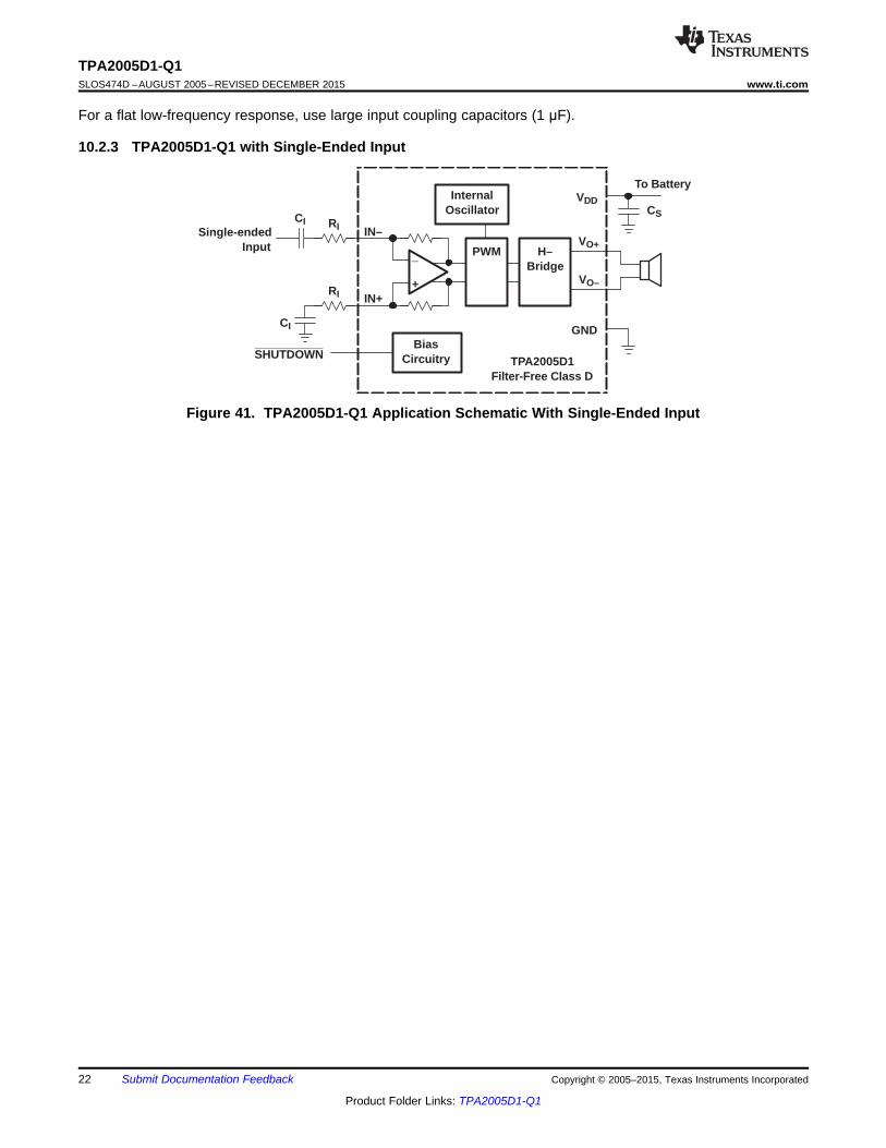
10.2.3 TPA2005D1-Q1 with Single-Ended Input
Figure 41. TPA2005D1-Q1 Application Schematic With Single-Ended Input
22 Submit Documentation Feedback Copyright © 2005–2015, Texas Instruments Incorporated
Product Folder Links: TPA2005D1-Q1

TPA2005D1-Q1www.ti.com SLOS474D –AUGUST 2005–REVISED DECEMBER 2015
11 Power Supply RecommendationsThe TPA2005D1-Q1 is designed to operate from an input voltage supply range between 2.5-V and 5.5-V.Therefore, the output voltage range of power supply should be within this range and well regulated. The currentcapability of upper power should not exceed the maximum current limit of the power switch.
11.1 Power Supply Decoupling CapacitorsThe TPA2005D1-Q1 requires adequate power supply decoupling to ensure a high efficiency operation with lowtotal harmonic distortion (THD). Place a low equivalent-series-resistance (ESR) ceramic capacitor, typically 0.1µF, within 2 mm of the VDD pin. This choice of capacitor and placement helps with higher frequency transients,spikes, or digital hash on the line. In addition to the 0.1 μF ceramic capacitor, it is recommended to place a 2.2µF to 10 µF capacitor on the VDD supply trace. This larger capacitor acts as a charge reservoir, providing energyfaster than the board supply, thus helping to prevent any droop in the supply voltage.
Copyright © 2005–2015, Texas Instruments Incorporated Submit Documentation Feedback 23
Product Folder Links: TPA2005D1-Q1

0,65 mm
0,38 mm
Solder Mask: 1,4 mm x 1,85 mm centered in package
0,7 mm
1,4 mm
Make solder paste a hatch pattern to fill 50%
3,3 mm
1,95 mm
0,33 mm plugged vias (5 places)
TPA2005D1-Q1SLOS474D –AUGUST 2005–REVISED DECEMBER 2015 www.ti.com
12 Layout
12.1 Layout Guidelines
12.1.1 Component LocationPlace all the external components very close to the TPA2005D1-Q1. The input resistors need to be very close tothe TPA2005D1-Q1 input pins so noise does not couple on the high-impedance nodes between the inputresistors and the input amplifier of the TPA2005D1-Q1. Placing the decoupling capacitor, CS, close to theTPA2005D1-Q1 is important for the efficiency of the class-D amplifier. Any resistance or inductance in the tracebetween the device and the capacitor can cause a loss in efficiency.
12.1.2 Trace WidthMake the high current traces going to pins VDD, GND, VO+ and VO– of the TPA2005D1-Q1 have a minimumwidth of 0.7 mm. If these traces are too thin, the TPA2005D1-Q1 performance and output power will decrease.The input traces do not need to be wide, but do need to run side-by-side to enable common-mode noisecancellation.
12.1.3 8-Pin QFN (DRB) LayoutUse the following land pattern for board layout with the 8-pin QFN (DRB) package. Note that the solder pasteshould use a hatch pattern to fill solder paste at 50% to ensure that there is not too much solder paste under thepackage.
Figure 42. TPA2005D1-Q1 8-Pin QFN (DRB) Board Layout (Top View)
24 Submit Documentation Feedback Copyright © 2005–2015, Texas Instruments Incorporated
Product Folder Links: TPA2005D1-Q1

SHUTDOWN
IN
IN
+
- OUT +
OUT -
0.1µF
Via to Bottom Ground Plane
Top Layer Ground Plane Top Layer Traces
Pad to Top Layer Ground Plane
Decoupling capacitor placed as close as
possible to the device
Input Resistors placed as close as
possible to the device
TPA2005D1
1
2
3
4
8
7
6
5
Thermal Pad
Via to Power Supply
SHUTDOWN
IN
IN
+
- OUT +
OUT -
0.1µF
Via to Bottom Ground Plane
Top Layer Ground Plane Top Layer Traces
Pad to Top Layer Ground Plane Thermal Pad
Decoupling capacitor placed as close as
possible to the device
Input Resistors placed as close as
possible to the device
TPA2005D1
1
2
3
4
8
7
6
5
Via to Power Supply
TPA2005D1-Q1www.ti.com SLOS474D –AUGUST 2005–REVISED DECEMBER 2015
12.2 Layout Example
Figure 43. TPA2005D1-Q1 DRB Package Layout Example
Figure 44. TPA2005D1-Q1 DGN Package Layout Example
Copyright © 2005–2015, Texas Instruments Incorporated Submit Documentation Feedback 25
Product Folder Links: TPA2005D1-Q1

TPA2005D1-Q1SLOS474D –AUGUST 2005–REVISED DECEMBER 2015 www.ti.com
13 Device and Documentation Support
13.1 Community ResourceThe following links connect to TI community resources. Linked contents are provided "AS IS" by the respectivecontributors. They do not constitute TI specifications and do not necessarily reflect TI's views; see TI's Terms ofUse.
TI E2E™ Online Community TI's Engineer-to-Engineer (E2E) Community. Created to foster collaborationamong engineers. At e2e.ti.com, you can ask questions, share knowledge, explore ideas and helpsolve problems with fellow engineers.
Design Support TI's Design Support Quickly find helpful E2E forums along with design support tools andcontact information for technical support.
13.2 TrademarksPowerPAD, E2E are trademarks of Texas Instruments.All other trademarks are the property of their respective owners.
13.3 Electrostatic Discharge CautionThese devices have limited built-in ESD protection. The leads should be shorted together or the device placed in conductive foamduring storage or handling to prevent electrostatic damage to the MOS gates.
13.4 GlossarySLYZ022 — TI Glossary.
This glossary lists and explains terms, acronyms, and definitions.
14 Mechanical, Packaging, and Orderable InformationThe following pages include mechanical, packaging, and orderable information. This information is the mostcurrent data available for the designated devices. This data is subject to change without notice and revision ofthis document. For browser-based versions of this data sheet, refer to the left-hand navigation.
26 Submit Documentation Feedback Copyright © 2005–2015, Texas Instruments Incorporated
Product Folder Links: TPA2005D1-Q1

PACKAGE OPTION ADDENDUM
www.ti.com 20-Nov-2015
Addendum-Page 1
PACKAGING INFORMATION
Orderable Device Status(1)
Package Type PackageDrawing
Pins PackageQty
Eco Plan(2)
Lead/Ball Finish(6)
MSL Peak Temp(3)
Op Temp (°C) Device Marking(4/5)
Samples
TPA2005D1DGNRQ1 ACTIVE MSOP-PowerPAD
DGN 8 2500 Green (RoHS& no Sb/Br)
CU NIPDAU Level-2-260C-1 YEAR -40 to 85 2005I
TPA2005D1DRBQ1 ACTIVE SON DRB 8 3000 Green (RoHS& no Sb/Br)
CU NIPDAU Level-2-260C-1 YEAR -40 to 85 BIQ
TPA2005D1TDGNRQ1 ACTIVE MSOP-PowerPAD
DGN 8 2500 Green (RoHS& no Sb/Br)
CU NIPDAU Level-2-260C-1 YEAR -40 to 105 2005T
(1) The marketing status values are defined as follows:ACTIVE: Product device recommended for new designs.LIFEBUY: TI has announced that the device will be discontinued, and a lifetime-buy period is in effect.NRND: Not recommended for new designs. Device is in production to support existing customers, but TI does not recommend using this part in a new design.PREVIEW: Device has been announced but is not in production. Samples may or may not be available.OBSOLETE: TI has discontinued the production of the device.
(2) Eco Plan - The planned eco-friendly classification: Pb-Free (RoHS), Pb-Free (RoHS Exempt), or Green (RoHS & no Sb/Br) - please check http://www.ti.com/productcontent for the latest availabilityinformation and additional product content details.TBD: The Pb-Free/Green conversion plan has not been defined.Pb-Free (RoHS): TI's terms "Lead-Free" or "Pb-Free" mean semiconductor products that are compatible with the current RoHS requirements for all 6 substances, including the requirement thatlead not exceed 0.1% by weight in homogeneous materials. Where designed to be soldered at high temperatures, TI Pb-Free products are suitable for use in specified lead-free processes.Pb-Free (RoHS Exempt): This component has a RoHS exemption for either 1) lead-based flip-chip solder bumps used between the die and package, or 2) lead-based die adhesive used betweenthe die and leadframe. The component is otherwise considered Pb-Free (RoHS compatible) as defined above.Green (RoHS & no Sb/Br): TI defines "Green" to mean Pb-Free (RoHS compatible), and free of Bromine (Br) and Antimony (Sb) based flame retardants (Br or Sb do not exceed 0.1% by weightin homogeneous material)
(3) MSL, Peak Temp. - The Moisture Sensitivity Level rating according to the JEDEC industry standard classifications, and peak solder temperature.
(4) There may be additional marking, which relates to the logo, the lot trace code information, or the environmental category on the device.
(5) Multiple Device Markings will be inside parentheses. Only one Device Marking contained in parentheses and separated by a "~" will appear on a device. If a line is indented then it is a continuationof the previous line and the two combined represent the entire Device Marking for that device.
(6) Lead/Ball Finish - Orderable Devices may have multiple material finish options. Finish options are separated by a vertical ruled line. Lead/Ball Finish values may wrap to two lines if the finishvalue exceeds the maximum column width.
Important Information and Disclaimer:The information provided on this page represents TI's knowledge and belief as of the date that it is provided. TI bases its knowledge and belief on informationprovided by third parties, and makes no representation or warranty as to the accuracy of such information. Efforts are underway to better integrate information from third parties. TI has taken and
PACKAGE OPTION ADDENDUM
www.ti.com 20-Nov-2015
Addendum-Page 2
continues to take reasonable steps to provide representative and accurate information but may not have conducted destructive testing or chemical analysis on incoming materials and chemicals.TI and TI suppliers consider certain information to be proprietary, and thus CAS numbers and other limited information may not be available for release.
In no event shall TI's liability arising out of such information exceed the total purchase price of the TI part(s) at issue in this document sold by TI to Customer on an annual basis.
OTHER QUALIFIED VERSIONS OF TPA2005D1-Q1 :
• Catalog: TPA2005D1
NOTE: Qualified Version Definitions:
• Catalog - TI's standard catalog product

TAPE AND REEL INFORMATION
*All dimensions are nominal
Device PackageType
PackageDrawing
Pins SPQ ReelDiameter
(mm)
ReelWidth
W1 (mm)
A0(mm)
B0(mm)
K0(mm)
P1(mm)
W(mm)
Pin1Quadrant
TPA2005D1DGNRQ1 MSOP-Power PAD
DGN 8 2500 330.0 12.4 5.3 3.4 1.4 8.0 12.0 Q1
TPA2005D1DRBQ1 SON DRB 8 3000 330.0 12.4 3.3 3.3 1.1 8.0 12.0 Q2
TPA2005D1TDGNRQ1 MSOP-Power PAD
DGN 8 2500 330.0 12.4 5.3 3.4 1.4 8.0 12.0 Q1
PACKAGE MATERIALS INFORMATION
www.ti.com 23-Nov-2015
Pack Materials-Page 1

*All dimensions are nominal
Device Package Type Package Drawing Pins SPQ Length (mm) Width (mm) Height (mm)
TPA2005D1DGNRQ1 MSOP-PowerPAD DGN 8 2500 367.0 367.0 35.0
TPA2005D1DRBQ1 SON DRB 8 3000 367.0 367.0 35.0
TPA2005D1TDGNRQ1 MSOP-PowerPAD DGN 8 2500 367.0 367.0 35.0
PACKAGE MATERIALS INFORMATION
www.ti.com 23-Nov-2015
Pack Materials-Page 2


IMPORTANT NOTICE
Texas Instruments Incorporated and its subsidiaries (TI) reserve the right to make corrections, enhancements, improvements and otherchanges to its semiconductor products and services per JESD46, latest issue, and to discontinue any product or service per JESD48, latestissue. Buyers should obtain the latest relevant information before placing orders and should verify that such information is current andcomplete. All semiconductor products (also referred to herein as “components”) are sold subject to TI’s terms and conditions of salesupplied at the time of order acknowledgment.TI warrants performance of its components to the specifications applicable at the time of sale, in accordance with the warranty in TI’s termsand conditions of sale of semiconductor products. Testing and other quality control techniques are used to the extent TI deems necessaryto support this warranty. Except where mandated by applicable law, testing of all parameters of each component is not necessarilyperformed.TI assumes no liability for applications assistance or the design of Buyers’ products. Buyers are responsible for their products andapplications using TI components. To minimize the risks associated with Buyers’ products and applications, Buyers should provideadequate design and operating safeguards.TI does not warrant or represent that any license, either express or implied, is granted under any patent right, copyright, mask work right, orother intellectual property right relating to any combination, machine, or process in which TI components or services are used. Informationpublished by TI regarding third-party products or services does not constitute a license to use such products or services or a warranty orendorsement thereof. Use of such information may require a license from a third party under the patents or other intellectual property of thethird party, or a license from TI under the patents or other intellectual property of TI.Reproduction of significant portions of TI information in TI data books or data sheets is permissible only if reproduction is without alterationand is accompanied by all associated warranties, conditions, limitations, and notices. TI is not responsible or liable for such altereddocumentation. Information of third parties may be subject to additional restrictions.Resale of TI components or services with statements different from or beyond the parameters stated by TI for that component or servicevoids all express and any implied warranties for the associated TI component or service and is an unfair and deceptive business practice.TI is not responsible or liable for any such statements.Buyer acknowledges and agrees that it is solely responsible for compliance with all legal, regulatory and safety-related requirementsconcerning its products, and any use of TI components in its applications, notwithstanding any applications-related information or supportthat may be provided by TI. Buyer represents and agrees that it has all the necessary expertise to create and implement safeguards whichanticipate dangerous consequences of failures, monitor failures and their consequences, lessen the likelihood of failures that might causeharm and take appropriate remedial actions. Buyer will fully indemnify TI and its representatives against any damages arising out of the useof any TI components in safety-critical applications.In some cases, TI components may be promoted specifically to facilitate safety-related applications. With such components, TI’s goal is tohelp enable customers to design and create their own end-product solutions that meet applicable functional safety standards andrequirements. Nonetheless, such components are subject to these terms.No TI components are authorized for use in FDA Class III (or similar life-critical medical equipment) unless authorized officers of the partieshave executed a special agreement specifically governing such use.Only those TI components which TI has specifically designated as military grade or “enhanced plastic” are designed and intended for use inmilitary/aerospace applications or environments. Buyer acknowledges and agrees that any military or aerospace use of TI componentswhich have not been so designated is solely at the Buyer's risk, and that Buyer is solely responsible for compliance with all legal andregulatory requirements in connection with such use.TI has specifically designated certain components as meeting ISO/TS16949 requirements, mainly for automotive use. In any case of use ofnon-designated products, TI will not be responsible for any failure to meet ISO/TS16949.
Products ApplicationsAudio www.ti.com/audio Automotive and Transportation www.ti.com/automotiveAmplifiers amplifier.ti.com Communications and Telecom www.ti.com/communicationsData Converters dataconverter.ti.com Computers and Peripherals www.ti.com/computersDLP® Products www.dlp.com Consumer Electronics www.ti.com/consumer-appsDSP dsp.ti.com Energy and Lighting www.ti.com/energyClocks and Timers www.ti.com/clocks Industrial www.ti.com/industrialInterface interface.ti.com Medical www.ti.com/medicalLogic logic.ti.com Security www.ti.com/securityPower Mgmt power.ti.com Space, Avionics and Defense www.ti.com/space-avionics-defenseMicrocontrollers microcontroller.ti.com Video and Imaging www.ti.com/videoRFID www.ti-rfid.comOMAP Applications Processors www.ti.com/omap TI E2E Community e2e.ti.comWireless Connectivity www.ti.com/wirelessconnectivity
Mailing Address: Texas Instruments, Post Office Box 655303, Dallas, Texas 75265Copyright © 2015, Texas Instruments Incorporated