toward the optimization of low-temperature solution …1147511/fulltext01.pdf · (cds) in zno nrs...
TRANSCRIPT

Linköping Studies in Science and Technology. Dissertation No. 1871
Toward the Optimization of Low-temperature Solution-based
Synthesis of ZnO Nanostructures for Device Applications
Hatim Alnoor
Physical Electronics and Nanotechnology Group
Department of Science and Technology (ITN)
Linköping University, SE-601 74 Norrköping, Sweden
2017 Norrköping

Cover Picture: The light emission from the fabricated heterojunction LEDs
within the thesis.
Photo credit: Thor Balkhed, Linköping University.
During the course of research underlying this thesis, Hatim Alnoor was enrolled in Agora Materiae, a multidisciplinary doctoral program at Linköping University, Sweden.
Hatim Alnoor, 2017
Printed by LiU-Tryck, Linköping, Sweden, 2017
ISBN: 978-91-7685-481-5
ISSN 0345-7524
Electronic publication: www.ep.liu.se

Dedicated to
My family


i
Abstract
One-dimensional (1D) nanostructures (NSs) of Zinc Oxide (ZnO)
such as nanorods (NRs) have recently attracted considerable research
attention due to their potential for the development of optoelectronic
devices such as ultraviolet (UV) photodetectors and light-emitting diodes
(LEDs). The potential of ZnO NRs in all these applications, however,
would require synthesis of high crystal quality ZnO NRs with precise
control over the optical and electronic properties. It is known that the
optical and electronic properties of ZnO NRs are mostly influenced by the
presence of native (intrinsic) and impurities (extrinsic) defects. Therefore,
understanding the nature of these intrinsic and extrinsic defects and their
spatial distribution is critical for optimizing the optical and electronic
properties of ZnO NRs. However, identifying the origin of such defects is
a complicated matter, especially for NSs, where the information on
anisotropy is usually lost due to the lack of coherent orientation. To
investigate the origin of these defects in more details and to fulfill all the
advantages of ZnO NRs in device applications several synthesis techniques
have been utilized. Among them, the low-temperature solution-based
methods, which are regarded as promising due to many advantages. It is
low-cost and offers the possibility of large-scale production and tuning the
properties of the final product through the synthesis parameters. However,
synthesizing reproducible ZnO NRs with optimized morphology,
orientation, electronic and optical properties by the low-temperature
solution-based methods remains a challenge.
Thus, the aim of this thesis is towards the optimization of the low-
temperature solution-based synthesis of ZnO NRs for device applications.
In this connection, we first started with investigating the effect of the

ii
precursor solution stirring durations on the deep level defects concentration
and their spatial distribution along the ZnO NRs. Then, by choosing the
optimal stirring time, we studied the influence of ZnO seeding layer
precursor’s types and its molar ratios on the density of interface defects.
The findings of these investigations were used to demonstrate ZnO NRs-
based heterojunction LEDs. The ability to tune the point defects along the
NRs enabled us further to incorporate cobalt (Co) ions into the ZnO NRs
crystal lattice, where these ions could occupy the vacancies or interstitial
defects through substitutional or interstitial doping. Following this, high
crystal quality vertically well-oriented ZnO NRs have been demonstrated
by incorporating a small amount of Co into the ZnO crystal lattice. Finally,
the influence of Co ions incorporation on the reduction of core-defects
(CDs) in ZnO NRs was systematically examined using electron
paramagnetic resonance (EPR).

iii
Acknowledgment
First, I must acknowledge and thank The Almighty Allah for
blessing, protection, and for guiding me through this journey and all my
life. This thesis would not have been feasible without the help, support,
and encouragement of many people to whom I am sincerely thankful.
I would like to express my deepest gratitude to my supervisor, associate
Prof. Omer Nour who believed in my knowledge during the first time I
met him and gave me this great opportunity to pursue my Ph.D. degree
under his supervision in the Physical Electronics and Nanotechnology
group. Thanks Omer for endless guidance, support, motivation,
encouragement, and patient help during the course of my Ph.D. Your
guidance, encouragement and enough freedom during my research
encouraged me to grow my knowledge and to become an independent
researcher. Also, I would like to thank, Omer and his family for the
generous hospitality at their home when I first arrived at Norrköping.
I express my profound gratitude to my co-supervisor, Prof. Magnus
Willander, for his support, encouragement, valuable discussions, positive
comments, and suggestions during my Ph.D. research course.
I am extremely grateful to all my co-authors Galia Pozina, Adrien
Savoyant, Volodymyr Khranovskyy, and Xianjie Liu for collaboration,
discussions, sharing your knowledge, suggestions, and for contribution in
the correction of some parts in the thesis manuscript.
Fredrik Eriksson thanks for your great help with XRD measurements and
for correcting the XRD part in this thesis.
Chan Oeurn Chey and Zia Ullah many thanks to all of you for teaching
me how to work in the lab and for the great help in some measurements.

iv
Ildiko Farkas thanks for helping with cutting samples.
Special thanks to Ann-Christin Norén for kind help and advice and taking
care of all our research administration work.
Anna Malmström, Lars Gustavsson, and Putte Eriksson for keeping the
lab running in good condition.
My thanks to Thor Balkhed for crediting the photo of the cover picture
and for help in the design of the cover picture.
The past and present Physical Electronics and Nanotechnology group
members for support, collaboration, and encouragement.
The past and present members of the research school Agora Materiae, and
special thanks to Prof. Per-Olof Holtz for organizing interesting seminars,
summer conference, study visits, and annual follow-up meetings. Also,
special thanks for Karina Malmström for taking care of all Agora
Materiae administration work.
I am very grateful to The National Center for Research (Sudan), National
Council for Training (Sudan), Ministry of Higher Education, and Scientific
Research (Sudan) and Linköping University for their financial support
during my Ph.D. study.
I would like to thank all friends and colleagues whom I met during my
Ph.D. for their support, encouragement and sharing a good time.
My uncle Eltahir, cousin Hamad and friends Ali and Adel for their
support for this scholarship to be possible.
I would like to share my depths gratitude with my family, in particular, my
parents, brothers and my sister for support, encouragement, prayers and for

v
wishing me all the best during my Ph.D. study and in my life. Also, I
express my appreciation to all the members of my family-in-law for their
support and engagement.
My lovely wife Tyseer words cannot express my gratitude to you. Thanks
for love, joyousness, patience, support, and being in my life.

vi

vii
List of the papers included in this thesis
1. Effect of precursor solution stirring on deep level defects concentration
and spatial distribution in low temperature aqueous chemical synthesis
of zinc oxide nanorods
Hatim Alnoor, Chan Oeurn Chey, Galia Pozina, Xianjie Liu,
Volodymyr Khranovskyy, Magnus Willander, and Omer Nur.
AIP Advances 5, 087180 (2015).
Contribution: I performed all the experimental work except the PL and
XPS, and I wrote the first draft of the manuscript.
2. Influence of ZnO seed layer precursor molar ratio on the density of
interface defects in low temperature aqueous chemically synthesized
ZnO nanorods/GaN light-emitting diodes
Hatim Alnoor, Galia Pozina, Volodymyr Khranovskyy, Xianjie Liu,
Donata Iandolo, Magnus Willander, and Omer Nur.
J. Appl. Phys. 119, 165702 (2016).
Contribution: I performed all the experimental work except the XPS,
PL, and AFM. I wrote the first version of the manuscript.
3. Seed layer synthesis effect on the concentration of interface defects
and emission spectra of ZnO nanorods/p-GaN light-emitting diode
Hatim Alnoor, Galia Pozina, Magnus Willander, and Omer Nur.
Phys. Status Solidi A 214, 1600333 (2017).
Contribution: I performed all the experimental work and wrote the first
version of the manuscript.
4. EPR investigation of pure and Co-doped ZnO oriented nanocrystals
A. Savoyant, H. Alnoor, S. Bertaina, O. Nur, and M. Willander.
Nanotechnology 28, 035705 (2017).

viii
Contribution: I performed the growth of the samples, did the SEM
measurements, and contributed to the writing of the first version of the
manuscript.
5. An effective low-temperature solution synthesis of Co-doped [0001]-
oriented ZnO nanorods
Hatim Alnoor, Adrien Savoyant, Xianjie Liu, Galia Pozina, Magnus
Willander, and Omer Nur.
J. Appl. Phys. 121, 215102 (2017).
Contribution: I performed all the experimental work except the EPR,
and XPS measurements. I wrote the first version of the manuscript.
6. Core-defect reduction in ZnO nanorods by cobalt incorporation
A. Savoyant, H. Alnoor, O. Pilone, O. Nur, and M. Willander.
Nanotechnology 28, 285705 (2017).
Contribution: I grew the samples and performed SEM measurements.
Also, I contributed to the writing of part of the first version of the
manuscript.

ix
List of the papers not included in this thesis
1. Fast synthesis, morphology transformation, structural and optical
properties of ZnO nanorods grown by seed-free hydrothermal method
Chan Oeurn Chey, Hatim Alnoor, Mazhar Ali Abbasi, Omer Nur, and
Magnus Willander.
Phys. Status Solidi A 211, 2611 (2014).
2. Fast piezoresistive sensor and UV photodetector based on Mn-doped
ZnO nanorods
Chan Oeurn Chey, Xianjie Liu, Hatim Alnoor, Omer Nur, and
Magnus Willander.
Phys. Status Solidi RRL 9, 87 (2015).
3. Zinc Oxide Nanostructure-Modified Textile and Its Application to
Biosensing, Photocatalysis, and as Antibacterial Material
Amir Hatamie, Azam Khan, Mohsen Golabi, Anthony P. F. Turner,
Valerio Beni, Wing Cheung Mak, Azar Sadollahkhani, Hatim Alnoor,
Behrooz Zargar, Sumaira Bano, Omer Nur, and Magnus Willander.
Langmuir 31, 10913 (2015).
Conference papers:
4. Zinc oxide nanostructures and its nano-compounds for efficient visible
light photo-catalytic processes
Rania E. Adam, Hatim Alnoor, Sami Elhag, Omer Nur, and Magnus
Willander.
Proc. SPIE 10105, Oxide-based Materials and Devices VIII, 101050X
(February 24, 2017); doi:10.1117/12.2254872.
5. Comparison between different metal oxide nanostructures and
nanocomposites for sensing, energy generation and energy harvesting

x
Magnus Willander, Hatim Alnoor, Sami Elhag, Zafar Hussain
Ibupoto, Eiman Satti Nour, and Omer Nur.
Proc. SPIE 9749, Oxide-based Materials and Devices VII, 97491L (27
February 2016); doi: 10.1117/12.2214513.

xi
List of Abbreviations
NSs Nanostructures
0D Zero-dimensional
1D One-dimensional
NRs Nanorods
2D Two-dimensional
ZnO Zinc oxide
UV Ultraviolet
LEDs Light-emitting diodes
CB Conduction band
VB Valence band
Co Cobalt
CDs Core defects
EPR Electron paramagnetic resonance
IEP Isoelectric point
NBE Near-band-edge emission
DLE Deep level emission
VO Oxygen vacancy
VZn Zinc vacancy
OH Hydroxyl ion

xii
Oi Oxygen interstitials
DMSs Diluted magnetic semiconductors
TMs Transition metals
RT-FM Room-temperature ferromagnetism
HMTA Hexamethylenetetramine
pH Power of hydrogen, Potential hydrogen
NH3 Ammonia
LT-ACS Low-temperature aqueous synthesis
Ag Silver
GaN Gallium nitrate
DI-water Deionized water
TF Thin film
NPs Nanoparticles
KOH Potassium hydroxide
h Hours
AFM Atomic force microscope
rpm Round per minute
Ni Nickel
Au Gold
RIE Reactive ion etching

xiii
FE-SEM Field-emission-scanning electron microscopy
XRD X-ray diffraction
XPS X-ray photoelectron spectroscopy
UHV Ultra-high vacuum
CL Cathodoluminescence
I-V Current –Voltage
SMUs Sources-measurement units
EL Electroluminescence
B Magnetic field
hν Photon energy
ΔE Energy difference
DL Deep level
Zni Zinc interstitial
Fe Iron
Mn Manganese
Cu Copper
PLE Photoluminescence excitation
ODMR Optically detected magnetic resonance

xiv

xv
List of figures
Figure 2.1: The unit cell of the ZnO hexagonal wurtzite-type structure ….6
Figure 2.2: Schematic illustration of the CB and VB structure of ZnO in
the vicinity of the fundamental bandgap………………….........................7
Figure 2.3: CL spectra of the ZnO synthesized on sapphire substrate using
the low-temperature aqueous chemical synthesis at 90 ºC from a growth
solution of a 0.075 M concentration of hexamethylenetetramine (HMTA)
and zinc nitrate hexahydrate in a deionized (DI)-water…………………...8
Figure 2.4: (a) Electronic configuration of the 3d7 of Co2+. (b) Level
diagram of Co2+ (3d7) ion in ZnO, under successive application of free ion,
crystal field, spin orbital, Zeeman coupling, and hyperfine interaction. Red
arrows depict allowed EPR transitions between non-degenerate hyperfine
levels…………………………………….................................................10
Figure 3.1: Surface topography of the prepared seeds layer using zinc (II)
acetate dihydrate and KOH with a molar ratio of (a) 1:1, (b) 1:3, and (c)
1:5 M. Scanned area: 2 x 2 µm……………………..................................15
Figure 3.2: Top-view FE-SEM images of the synthesized pure NRs grown
using 0.05 M concentration of zinc nitrate and 0.075 M concentration of
HMTA at 80 C for 6 h.………………………………………………….16
Figure 3.3: Top-view FE-SEM images of the synthesized Co-doped ZnO
NRs grown using the first and second method for preparing the synthesis
solution (a), and (b), respectively………………………………………..17
Figure 3.4: (a) Schematic diagram illustrating the fabricated
heterojunction LEDs, (b) Cross-sectional SEM image of the synthesized n-
ZnO NRs on the p-GaN substrate, (c) Optical photograph of the fabricated
xvi
heterojunction LEDs on p-GaN substrate, and (d) Optical photograph of
the fabricated heterojunction LEDs under forwarding bias……………...18
Figure 4.1: Schematic illustration of x-ray diffraction………………….21
Figure 4.2: Schematic illustration of the XPS experiment………………22
Figure 4.3: Schematic illustration of the signals from the sample under
electron beam bombardment…………………………………………….23
Figure 4.4: Optical photograph illustrating the light emission from the
fabricated ZnO NRs/ GaN heterojunction LED under forwarding bias….24
Figure 4.5: Schematic illustration of the EPR experiment………………25
Figure 4.6: Schematic illustrations of the NRs samples and definition of
the angle θ between the magnetic field B and the c-axis of the NRs. The
microwave magnetic field B1 is perpendicular to both B and C………….26
Figure 5.1: Top-view FE-SEM images of the synthesized ZnO NRs
prepared under stirring durations of (a) 1 h, (b) 3 h, (C) 5 h, (c), and (d) 15
h, respectively…………………………………………………………...28
Figure 5.2: CL spectra of the individual NRs measured in cross-sectional
view. The insets display the cross-sectional SEM images of the NRs with
a sign of the spots where the CL spectra were recorded. For clarity, spectra
have been offset in the vertical direction………………………………...30
Figure 5.3: CL spectra of n-ZnO NRs / p-GaN heterostructure recorded in
cross-sectional view. The inset displays a typical cross-sectional SEM
image of the n-ZnO NRs / p-GaN heterostructure with the sign of the point
where the CL spectra were recorded…………………………………….32

xvii
Figure 5.4: EL spectra as a function of the forward bias voltage of device
(a) 1, (b) 3, and (c) 5, respectively. The insets present the corresponding
light emission images at 24 V. (d) The integrated EL intensities of three
devices as a function of the forward bias voltage………………………...33
Figure 5.5: Integrated EL intensities of all the three devices as a function
of the forward injection current. The solid lines represent the fitting results
based on the power law L= cIm ……………….........................................35
Figure 5.6: (a) CL spectra of the n-ZnO NRs / p-GaN heterostructures
recorded in top-view mode. For clarity, all the spectra are normalized to
the DL emission and shifted in vertical direction. (b) Cross-sectional view
CL spectra of the n-ZnO NRs/p-GaN heterostructures interface. The insets
display the synthesized n-ZnO NRs/p-GaN heterostructures in cross-
sectional view with a sign of the points where the CL spectra were
measured………………………………………………………………...36
Figure 5.7: EL spectra of (a) ZK device, and (b) ZKH device, as a function
of the bias voltage. The insets show the corresponding light emission
images at 15 V. (c) Gaussian decomposition of the dominant yellow
emission of the ZKH device at a bias voltage of 15 V. (d) EL spectra of the
two devices under a bias voltage of 15 V………………………………...38
Figure 5.8: (a) The integrated EL intensities of the ZH and ZKH devices
as a function of bias voltage. (b) Role of injection currents. The solid lines
in Figure b illustrated the fitting results based on the power law L=
CIn……………………………………………………………………….39
Figure 5.9: Top-view SEM images of the pure ZnO (S0) and 5% Co-doped
ZnO NRs (S2)..……………………………………….............................40
Figure 5.10: X-band EPR spectra (5 G modulation) at each step of the NRs
synthesis. EPR of (a) The sample holder, (b) Sapphire substrate, (c) ZnO

xviii
seed layer, (d) Pure ZnO NRs, and (e) 5% of Co-doped ZnO NRs. No
baseline subtraction or exponential smoothing….………………………41
Figure 5.11: Experimental X-band EPR spectra(1G modulation) of sample
S0 showing the g ~ 1.96 signal for B // z (θ = 0º) and B z (θ = 90º),
recorded at T = 5 K. The upper x-axis gives the corresponding g factor
value. …………………………………………………………………....42
Figure 5.12: X-band EPR spectra of sample S2 for parallel (θ = 0º) and
perpendicular (θ = 90º) orientation of B field. The CD and sample holder
(SH) signals are shown. Gravity centers of the Co2+ signal for both
orientations are shown..……………………………………....................43
Figure 5.13: Top-view FE-SEM images of pure (M0) and Co-doped ZnO
NRs synthesized using approaches M1 and M2, respectively…………...44
Figure 5.14: XRD patterns of the synthesized pure (M0) and Co-doped
ZnO NRs (M1and M2). The inset shows the normalized XRD data for the
(002) peaks, indicating peak shifts……………........................................45
Figure 5.15: EPR spectra of Co-doped ZnO NRs (M1 and M2) for parallel
(θ = 0º) and perpendicular (θ = 90º) orientation of magnetic field, recorded
at T = 5 K. ……………………………………….....................................46
Figure 5.16: CL spectra of the synthesized pure and Co-doped ZnO NRs
synthesized utilizing different synthesis preparation approaches as shown.
The inset demonstrates the red-shift in the UV peak. For clarity, the spectra
are normalized to the NBE intensity……………………………………..47
Figure 5.17: Schematic diagram of the cross-sectional view of the
synthesized pure and Co-doped ZnO NRs including Zni+ as core-defect and
oxygen vacancies/interstitials as surface defects, respectively……..........48

xix
Figure 5.18: Evolution of the CD signal with the cobalt concentration
within the synthesis solution. The line of the 0% is divided by 100..…….50
Figure 5.19: Anisotropy of the EPR CD signal in pure (0% Co) and Co-
doped (0.5%) samples, with respect to the magnetic field orientation,
recorded at T=6 K. Sapphire defect (SD) signal present in the 0.5% sample
is shown for the θ = 0 orientation..……………………………………...52

xx

xxi
Abstract…………………………………………………………………...i
Acknowledgment………………………………………………………..iii
List of the papers included in the thesis………………………………….vii
List of the papers not included in the thesis……………………………....ix
List of Abbreviations…………………………………………………….xi
List of figures…………………………………………………………....xv
1. Introduction…………………………………………………………..1
2. Material characteristics………………………………………………5
2.1 ZnO characteristics…....................................................................5
2.1.1 Crystal structure.…..........................................................5
2.1.2 Electronic band structure…..............................................6
2.1.3 Optical characteristics…..................................................7
2.2 Co-doped ZnO characteristics.......................................................8
3. Synthesis methods…..........................................................................11
3.1 Hydrothermal synthesis methods……………….........................11
3.2 ZnO seed layer preparation..........................................................13
3.3 Synthesis of ZnO NRs…………………………………………..14
3.4 Synthesis of Co-doped ZnO NRs…….........................................15
3.5 N-ZnO NRs/p-GaN-based heterojunction LEDs.........................17
4. Characterization tools........................................................................19
4.1 Scanning electron microscopy (SEM)….....................................19
4.2 X-ray diffraction (XRD)…...........................................................20
4.3 X-ray photoelectron spectroscopy (XPS)…….............................21
4.4 Photoluminescence (PL) spectroscopy.........................................22
4.5 Cathodoluminescence (CL) spectroscopy....................................22
4.6 Current –Voltage (I-V) measurements..........................................23

xxii
4.7 Electroluminescence (EL) measurements……………………….24
4.8 Electron Paramagnetic Resonance (EPR) measurements.............24
5. Results and discussion…...................................................................27
5.1 The effect of precursor (solutions) stirring durations on the optical
properties of ZnO NRs………………………….........................27
5.2 Influence of ZnO seed layer precursor molar ratios on the emission
properties of n-ZnO NRs-based heterojunction LEDs………….31
5.3 Influence of ZnO seed layer precursor types on the emission
properties of n-ZnO NRs-based heterojunction LEDs………….35
5.4 Synthesis of Co-doped ZnO oriented NRs………......................39
5.5 The influence of the synthesis solution mixing on Co-doped ZnO
NRs……………………………………………………………..43
5.6 Core-defect reduction in ZnO NRs by Co incorporation..............49
6. Research summary and future work…..............................................53
7. References.………………………………………………….............57

1
1. Introduction
The ability to synthesize materials at the nanoscale range not only
offers a way for exploring their fascinating physical, chemical, mechanical
and biological properties but also for their potential as building blocks for
the development of a diverse range of emerging electronic devices and
systems.[1-3] Synthesis of such remarkable nanomaterials can be achieved
by either assembling the atoms/molecules (bottom-up approach) or
sculpting the bulk solids into small atomic level pieces (top-down
approach) to obtain the desired nanostructures (NSs). Such NSs materials
can typically structure into, zero-dimensional (0D) e.g., quantum dot
/nanoparticles [4-8], one-dimensional (1D) e.g., nanowires and nanorods
(NRs)[9-11], and two-dimensional (2D) e.g., nanosheets and nanowalls.[12-15]
Compared to 0D and 2D, 1D NSs have the advantage of the possibility of
being vertically oriented, which is crucial for many device applications.[16]
Among a variety of metal oxides, zinc oxide (ZnO) have a preference of
the favorable formation in all NSs forms mentioned above on any substrate
being crystalline or amorphous.[9,17-19] Moreover, ZnO possesses excellent
optical and electronic properties.[20-23] All these features make ZnO as one
of the most promising materials for a diversity of applications. In
particular, ZnO NRs have recently attracted considerable research interest
due to their potential for the development of optoelectronic devices e.g.,
ultraviolet (UV) photodetectors [24-27], light-emitting diodes (LEDs) [20,22,23]
and solar cells.[28] The potential of ZnO NRs in all these applications,
however, would require synthesis of high crystal quality ZnO NRs with
precise control over the morphology, alignment, optical and electronic
properties.[22,23,29] Broadly, it is well known that the presence of native
(intrinsic) and impurities (extrinsic) defects have a high impact on the
electronic and optical properties of ZnO NRs.[20-23,30-33] In particular, in all

2
luminescence processes, these defects in ZnO are engaged as steps in the
excitation and recombination paths, and thus influence the absorbed
/emitted light properties. Also, these defects play an important part in the
electrical conductivity in semiconductors by the ability to provide
delocalized electrons in the conduction band (CB) and holes in the valence
band (VB). Consequently, the knowledge of understanding the origin and
the control of these defects, as well as the relationship between both, are
essential factors for optimizing the optical and electronic properties of ZnO
NRs.[20-23,30-33] However, identifying the nature of such defects is a complex
issue, particularly in NSs, where the information on anisotropy is usually
lost due to the lack of coherent orientation.[34] To investigate the origin of
these defects in more details and to fulfill all the advantages of ZnO NRs
in device applications several synthesis techniques have been utilized.
Among them, the low-temperature solution-based methods, which are
regarded as promising methods due to many advantages. It is low-cost and
offers the possibility of large-scale production and tuning of the properties
of the final product through the synthesis parameters.[9,18,35] However,
synthesizing reproducible ZnO NRs with optimized morphology,
orientation, electronic and optical properties by the low-temperature
solution-based methods remains a challenge.
Thus, the aim of this thesis is towards the optimization of the low-
temperature solution-based synthesis of ZnO NRs for device applications.
In this connection, we first started with investigating the effect of the
precursor solution stirring durations on the deep level defects concentration
and their spatial distribution along the ZnO NRs. Then, by choosing the
optimal stirring time, we studied the influence of ZnO seeding layer
precursor’s types and its molar ratios on the density of interface defects.
The findings of this investigation were used to demonstrate ZnO NRs-

3
based heterojunction LEDs. The ability to tune the point defects along the
NRs enabled us further to incorporate cobalt (Co) ions into the ZnO NRs
crystal lattice, where these ions could occupy vacancies or interstitial
defects through substitutional or interstitial doping. Following this, high
crystal quality vertically well-oriented ZnO NRs have been demonstrated
by incorporating a small amount of Co2+ into the ZnO crystal lattice.
Finally, the influence of Co2+ ions incorporation on the reduction of core-
defects (CDs) in ZnO NRs was systematically examined using electron
paramagnetic resonance (EPR).

4

5
2. Material characteristics
2.1. ZnO characteristics
Having a direct wide bandgap of about 3.37 eV (at room
temperature) with relatively high exciton binding energy (60 meV) and
possessing unique luminescence properties enable ZnO to be an attractive
material for many applications.[20,21] Further, ZnO is considered as one of
the most promising semiconductor materials for the development of
optoelectronic devices.[20-23] Beside the fact that it is a biocompatible
material, ZnO has a high isoelectric point (IEP ~ 9.5), and exhibits large
surface area/volume ratio in its nanostructured forms, and hence is also
regarded as excellent material for sensing applications.[36] Moreover, due
to the lack of non-central symmetry, ZnO possesses relatively strong
piezoelectric effect, which makes it an attractive material for some energy-
harvesting applications.[37,38] The fundamental structural, electronic and
optical properties of ZnO is briefly introduced in this chapter.
2.1.1. Crystal structure
ZnO is a member of the II-IV binary compound semiconductor
family, and its crystal is either cubic zinc blend or wurtzite-type structure.
In the wurtzite structure of ZnO, the Zn and O atoms are organized into a
hexagonal form where one Zn2+ ion is enclosed tetrahedrally by four O2-
ions and vice versa as shown in the unit cell in Figure 2.1.[21] The unit cell
of the hexagonal wurtzite structure of ZnO has lattice parameters of about
a = 0.32498 nm and c = 5.2066 nm with the ratio of c/a = 1.60.[21]
Moreover, the hexagonal wurtzite structure of ZnO is characterized by six
nonpolar {10ī0} surfaces covered by polar Zn (0001) and oxygen (000ī)
basal planes. These polar surfaces are electrostatically unstable and hence
is leading to the growth habit along the c-axis producing 1D ZnO NRs.[39]

6
Figure 2.1: The unit cell of the ZnO hexagonal wurtzite-type structure.[21]
2.1.2. Electronic band structure
The electronic band gap structure is the most significant property of
ZnO, and it is critical when considering it for optoelectronics applications.
It is known that at ambient conditions, ZnO is a direct band gap material
where the energy difference (3.37 eV) between the lowermost conduction
band (CB) and uppermost valence band (VB) occurs at the same point in
the Brillouin zone which is known as the Г-point as shown in Figure 2.2.[21]
Due to the high ionic feature of ZnO, the bottom of the CB is principally
formed by the 4s level of Zn2+ or antibonding sp3 hybrid states, while the
VB is made by the 2p level of O2- or the bonding sp3 orbitals.[21] As
predicted by the group theory the bottom of the CB has a Г1 symmetry
without the inclusion of spin and symmetry Г1 Г7 = Г7 with spin as shown
in Figure 2.2. The VB is splitted without spin into two states, Г5 and Г1
under the effect of the hexagonal crystal field of ZnO. Moreover, the
inclusion of the spin added further splitting of the VB and provided three
twofold-degenerate sub-VBs with the symmetries of ( Г1 Г5) Г7 = Г7
Г9 Г7 as shown in Figure 2.2. These three sub-VBs are often labeled
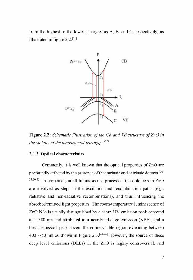
7
from the highest to the lowest energies as A, B, and C, respectively, as
illustrated in figure 2.2.[21]
Figure 2.2: Schematic illustration of the CB and VB structure of ZnO in
the vicinity of the fundamental bandgap. [21]
2.1.3. Optical characteristics
Commonly, it is well known that the optical properties of ZnO are
profoundly affected by the presence of the intrinsic and extrinsic defects.[20-
23,30-35] In particular, in all luminescence processes, these defects in ZnO
are involved as steps in the excitation and recombination paths (e.g.,
radiative and non-radiative recombinations), and thus influencing the
absorbed/emitted light properties. The room-temperature luminescence of
ZnO NSs is usually distinguished by a sharp UV emission peak centered
at ~ 380 nm and attributed to a near-band-edge emission (NBE), and a
broad emission peak covers the entire visible region extending between
400 -750 nm as shown in Figure 2.3.[40-44] However, the source of these
deep level emissions (DLEs) in the ZnO is highly controversial, and

8
possibly these DLE peaks are composed of multiple sub-bands e.g., green,
yellow and orange-red bands. The green emission band centered at ~ 500
–550 nm, is usually ascribed to oxygen vacancy (VO) or zinc vacancy
(VZn).[20,33,45] The yellow emission band centered between 550 – 600 nm
and the red emission band centered at ~ 620 – 750 nm are usually assigned
the presence of OH groups and to the oxygen interstitials (Oi) present on
the surface of the ZnO NRs.[33,40,43,46]
Figure 2.3: Cathodoluminescence (CL) spectrum of ZnO NRs synthesized
on a sapphire substrate using the low-temperature aqueous chemical
synthesis at 90 ºC from a growth solution of a 0.075 M concentration of
hexamethylenetetramine (HMTA) and zinc nitrate hexahydrate in
deionized (DI)-water.
2.2. Co-doped ZnO characteristics
Doping is a major method to control the semiconductors properties
e.g., optical, electronic and magnetic properties. ZnO NSs-based diluted
magnetic semiconductors (DMSs), where a low concentration of 3d

9
transition metals (TMs) ions is diluted into the ZnO crystal lattice, show
great promise for the development of spintronics and magneto-optical
devices.[47-50] The potential of this ZnO NRs-based DMSs in spintronics
applications would require the presence of the room-temperature
ferromagnetism (RT-FM), which is probably related to the successful
substitution of these DMSs ions into the ZnO crystal lattice.[48-50] Beside,
the crystal quality, optical and electronic properties of ZnO NRs-based
DMSs together with control over the morphology and alignment is critical
in device applications. Among a variety of 3d TMs ions in ZnO NRs-based
DMSs, Co is of particular interest due to its a unique optical and magnetic
property.[51,52] Although considerable research progress has been made to
synthesize Co-doped ZnO NRs, most of the research has focused on
probing their optical and magnetic properties.[48-51] However, the synthesis
of a high crystal quality of Co-doped ZnO with the successful substitution
of Co2+ in the host crystal site is still lacking, which will probably lead to
better understanding of the origin of the RT-FM in ZnO. Figure 2.4 (a)
shows the electronic configuration of the 3d7 of Co2+ and (b) illustrates the
level diagram of Co2+ (3d7) ion in ZnO where first, a free ion (gas):
Coulomb interaction leads to 4F (S=3/2, L=3) ground state, by Hund’s rule.
Then in a tetrahedral crystal field (case of the nearest neighbors O2- ions
around Co2+), the ground state becomes 4S (S = 3/2, L = 0) which is called
orbital momentum quenching (by the crystal field). Then by including the
spin orbit and the axial part of the crystal field, the ground state is split by
2D, where D is the axial spin anisotropy parameter, which is positive (easy
plane) and it is about 2.5 cm-1. The ground state is then doubly degenerate
(+/- 1/2 projection of the S = 3/2), and the state just above also (+/- 3/2
projection of S=3/2). Finally, taking into account the nuclear spin and the
hyperfine interaction each projection is separated into eight levels.

10
Figure 2.4: (a) Electronic configuration of the 3d7 of Co2+. (b) Level
diagram of Co2+ (3d7) ion in ZnO, under successive applications of free
ion, crystal field, spin orbital, Zeeman coupling, and hyperfine interaction.
Red arrows depict allowed EPR transitions between non-degenerate
hyperfine levels.
11
3. Synthesis methods
3.1. Hydrothermal synthesis methods
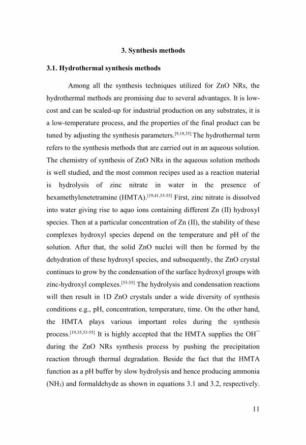
Among all the synthesis techniques utilized for ZnO NRs, the
hydrothermal methods are promising due to several advantages. It is low-
cost and can be scaled-up for industrial production on any substrates, it is
a low-temperature process, and the properties of the final product can be
tuned by adjusting the synthesis parameters.[9,18,35] The hydrothermal term
refers to the synthesis methods that are carried out in an aqueous solution.
The chemistry of synthesis of ZnO NRs in the aqueous solution methods
is well studied, and the most common recipes used as a reaction material
is hydrolysis of zinc nitrate in water in the presence of
hexamethylenetetramine (HMTA).[19,41,53-55] First, zinc nitrate is dissolved
into water giving rise to aquo ions containing different Zn (II) hydroxyl
species. Then at a particular concentration of Zn (II), the stability of these
complexes hydroxyl species depend on the temperature and pH of the
solution. After that, the solid ZnO nuclei will then be formed by the
dehydration of these hydroxyl species, and subsequently, the ZnO crystal
continues to grow by the condensation of the surface hydroxyl groups with
zinc-hydroxyl complexes.[53-55] The hydrolysis and condensation reactions
will then result in 1D ZnO crystals under a wide diversity of synthesis
conditions e.g., pH, concentration, temperature, time. On the other hand,
the HMTA plays various important roles during the synthesis
process.[19,35,53-55] It is highly accepted that the HMTA supplies the OH¯
during the ZnO NRs synthesis process by pushing the precipitation
reaction through thermal degradation. Beside the fact that the HMTA
function as a pH buffer by slow hydrolysis and hence producing ammonia
(NH3) and formaldehyde as shown in equations 3.1 and 3.2, respectively.

12
[19,53-55] Also, it is proposed that during the synthesis process of ZnO crystal,
the HMTA attaches to the nonpolar surface of ZnO NRs and hence prohibit
the access of the Zn2+ to them and therefore leaving only the polar surface
for epitaxial growth. The chemical reactions for obtaining ZnO NSs in an
aqueous solution when zinc nitrate and HMTA are used as a reaction
material can be summarized in the following equations:[53-55]
Decommission reaction:
C6H12N4 + 6H2O ↔ 4NH3 + 6HCHO (3.1)
Hydroxyl supply reaction:
NH3 + H2O ↔ NH4+ + OH− (3.2)
Super-saturation reaction:
Zn2+ + 2HO− → Zn(OH)2 (3.3)
ZnO NRs synthesis reaction:
Zn(OH)2 → ZnO(S) + H2O (3.4)
Controlling all these reactions play a significant effect on the final
properties of the synthesized ZnO NSs.[19,55]
In this thesis, pure and Co-doped ZnO NRs were synthesized by
the low-temperature aqueous synthesis (LT-ACS) at 80-90 ºC on silver
(Ag) coated glass, p-type GaN, and sapphire substrates, respectively. In the
experiments, we mainly investigated the synthesis conditions e.g., stirring
durations of the synthesize solutions, ZnO seeding layer precursors types,
and its molar ratios to obtain vertically-well aligned ZnO NRs with tuned
defects emission along the NRs and at the interfaces between the NRs and
the substrates.[56-58] Moreover, high crystal quality well-oriented Co-doped

13
ZnO NRs were also synthesized by manipulating the way of mixing the
synthesizer solution.[34,52,59] All these parameters were precisely selected
considering that the final properties of the ZnO NRs are susceptible to the
synthesis conditions. A typical LT-ACS of ZnO NSs consists of two main
steps: first, a clean substrate is subjected to spin coating with a ZnO seed
layer and then ZnO NSs are subsequently, synthesized from a zinc ion
containing solution. It is to be noted that before these two steps, all
substrates used in this work were first cleaned with acetone, isopropanol,
and deionized water (DI-water) for 5 minutes each to eliminate any
residuals, and were then dried up using blowing nitrogen. We found that
these steps play a significant role in the final structural and optical quality
of the synthesized ZnO NRs.
3.2. ZnO seed layer preparation
In the LT-ACS it is widely accepted that the presence of the seed
layer is required to promote nucleation sites for ZnO NRs synthesis by
lowering the thermodynamic barrier between heterogeneous materials.[35]
Also, it is known that the properties of the seed layer have a significant
impact on the quality of ZnO NRs synthesis and consequently on their final
properties.[60-65] In general, the seed layer can be prepared in the form of
thin film (TF) or nanoparticles (NPs) and then can be deposited on a
certain substrate by several deposition techniques e.g., sputtering, spin
coating and dip coating.[18,35,60] In particular, the NPs seed layer is often
prepared by the dissolution of zinc acetate dihydrate (Zn(CH3COO)2.H2O)
in organic solvents e.g., methanol, and the subsequent addition of a basic
aqueous solution e.g., potassium hydroxide (KOH).[35,53] In this thesis, two
types of seed layers were prepared, and their effect on the performance of
the synthesized ZnO-based heterojunction LEDs was systematically

14
studied.[57,58] The first seed layer is made by dissolution 0.01 M
concentration of zinc (II) acetate dihydrate in methanol and then heated at
60 ºC on a hotplate under continuous stirring. Subsequently, a solution of
KOH in methanol with different concentrations of 0.01, 0.03 and 0.05 M,
respectively, was added dropwise to zinc (II) acetate solution. Then the
whole solution was kept on a hotplate for 2 hours (h).[57] Figure 3.1 shows
the atomic force microscopy (AFM) image of the prepared seed layer with
molar ratios of 1:1, 1:3 and 1:5 M, respectively. The second seed layer was
made by following the same procedure used for the previous one where a
mixture of KOH and HMTA with 0.05 M concentration were dissolved in
methanol and were then added dropwise to a prepared 0.01 M
concentration of zinc (II) acetate dihydrate in methanol.[58] For the
synthesis of the pure and Co-doped ZnO NRs, the prepared seed layer
solutions were then spun coated 3-4 times on the substrates with a spin
speed of 3000 round per minute (rpm) for 3 minutes. This step was then
followed by annealing in a normal laboratory oven for 10 minutes at 120
ºC and subsequently submerged in the ZnO synthesis solution. Finally, the
synthesized ZnO NRs on the seeded substrates were rinsed with DI-water
to remove any residuals and were finally dried using blowing nitrogen for
further characterization.
3.3. Synthesis of ZnO NRs
After optimization of the many synthesis parameters, to achieve
highly dense and vertically aligned ZnO NRs with tuned optical properties.
The following conditions were utilized to synthesize the ZnO NRs in the
entire thesis. The synthesis solutions used were 0.05 M concentration for
the zinc nitrate and 0.075 M concentration for the HMTA with a molar
ratio of 1:2.[56-58] Then we investigated the effect of stirring durations of the

15
synthesis solutions on the optical properties of the ZnO NRs.[56] Four
synthesis precursor's (solution) consisting of zinc nitrate and HMTA were
dissolved separately in 100 ml DI-water each and were then carefully
mixed and stirred at room-temperature for 1, 3, 5 and 15 h, respectively,
with a stirring speed of 600 rpm. The ZnO NRs were then synthesized by
immersing a seeded glass substrate coated with Ag inside the synthesis
solution while keeping them in a preheated oven at 80 C for 6 h.
Afterward, the samples were cleaned with DI-water to remove any
residuals and were finally dried using blowing nitrogen.
Figure 3.1: Surface topography of the prepared seed layer using zinc (II)
acetate dihydrate and KOH with molar ratios of (a ) 1:1, (b) 1:3, and (c)
1:5 M. Scanned area: 2 x 2 µm.
Figure 3.2 shows the top-view FE-SEM image of the synthesized
ZnO NRs. The effect of stirring durations on the concentration and spatial
distribution of the deep level defects in the synthesized ZnO NRs were
systematically studied.[56]
3.4. Synthesis of Co-doped ZnO NRS
For the synthesis of high crystal quality well-oriented pure and
Co-doped ZnO NRs, two different processes for preparing the synthesis
solution were used.[34,52,59] The first process for preparing the synthesis

16
solution is carried out by making a 0.075 M concentration of HMT
separately in 100 ml of DI-water and subsequently stirred at room-
temperature for 1 h. Then, diluted solutions of Cobalt (II) acetate
tetrahydrate in 60 ml of DI-water with different atomic concentrations
were mixed with the HMTA solution and stirred for 15 h. After that, a
0.075 M concentration of zinc nitrate hexahydrate prepared in 40 ml of DI-
water was added dropwise to the solutions mixed above and stirred for
additional 3 h. Finally, the seeded sapphire substrates were then submerged
vertically inside the synthesis solutions and kept in the oven at 90 °C for 6
h. After the NRs growth, the samples were rinsed with DI-water to remove
any residuals and finally dried using blowing nitrogen.[59] The second
process was done by mixing a 0.075 M concentration of zinc nitrate, and
HMTA prepared separately in 70 ml DI-water each and were then mixed
and stirred for 15 h. Then, diluted solutions of Cobalt (II) nitrate
hexahydrate in 40 ml DI-water with different atomic concentrations was
added dropwise to the solution above and stirred for further 3 h.[34,52,59]
Figure 3.2: Top view FE-SEM images of the synthesized pure NRs grown
using 0.05 M concentration of zinc nitrate and 0.075 M concentration of
HMTA at 80 ◦C for 6 h.
17
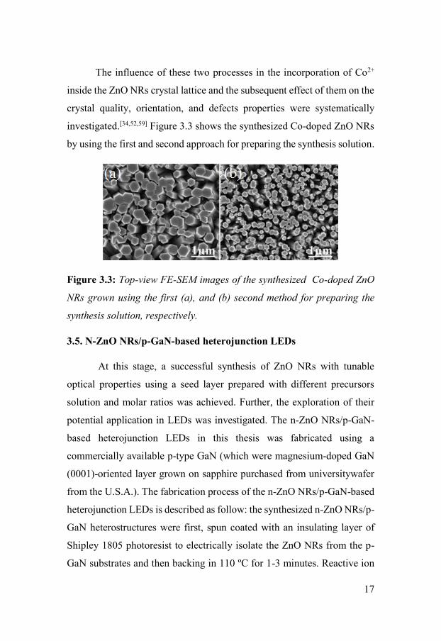
The influence of these two processes in the incorporation of Co2+
inside the ZnO NRs crystal lattice and the subsequent effect of them on the
crystal quality, orientation, and defects properties were systematically
investigated.[34,52,59] Figure 3.3 shows the synthesized Co-doped ZnO NRs
by using the first and second approach for preparing the synthesis solution.
Figure 3.3: Top-view FE-SEM images of the synthesized Co-doped ZnO
NRs grown using the first (a), and (b) second method for preparing the
synthesis solution, respectively.
3.5. N-ZnO NRs/p-GaN-based heterojunction LEDs
At this stage, a successful synthesis of ZnO NRs with tunable
optical properties using a seed layer prepared with different precursors
solution and molar ratios was achieved. Further, the exploration of their
potential application in LEDs was investigated. The n-ZnO NRs/p-GaN-
based heterojunction LEDs in this thesis was fabricated using a
commercially available p-type GaN (which were magnesium-doped GaN
(0001)-oriented layer grown on sapphire purchased from universitywafer
from the U.S.A.). The fabrication process of the n-ZnO NRs/p-GaN-based
heterojunction LEDs is described as follow: the synthesized n-ZnO NRs/p-
GaN heterostructures were first, spun coated with an insulating layer of
Shipley 1805 photoresist to electrically isolate the ZnO NRs from the p-
GaN substrates and then backing in 110 ºC for 1-3 minutes. Reactive ion

18
etching (RIE) with oxygen plasma was then used to remove the photoresist
from the ZnO NRs surface and expose the NRs tip for the metal contacts.
Finally, Ni/Au (15 nm / 35 nm) were thermally evaporated onto the p-GaN
substrates and Ag (40 nm) on the exposed ZnO NRs tip to serve as p-type
and n-type contact electrodes, respectively.[57,58] The p-type and n-type
contacts were evaporated in a circular area of diameter ~ 2 mm. The
fabrication process is illustrated in Figure 3.4.
Figure 3.4: (a) Schematic diagram illustrating the fabricated
heterojunction LEDs, (b) Cross-sectional SEM image of the synthesized n-
ZnO NRs on the p-GaN substrate, (c) Optical photograph of the fabricated
heterojunction LEDs on a p-GaN substrate, and (d) Optical photograph of
the fabricated heterojunction LEDs under forwarding bias.

19
4. Characterization tools
Several characterization tools have been employed to get insights
into morphology and the structural, optical, electrical and electronic
properties of the synthesized pure and Co-doped ZnO NRs. Field-
emission-scanning electron microscopy (FE-SEM) was utilized to
characterize the morphological properties of the synthesized pure and Co-
doped ZnO NRs. The crystalline quality and electronic structure were
investigated using the x-ray diffraction (XRD) and electron paramagnetic
resonance (EPR), respectively. Also, EPR was applied to confirm the
successful substitution of Co inside the ZnO crystal lattice. Then, micro-
photoluminescence (µ-PL), cathodoluminescence (CL), and x-ray
photoelectron spectroscopy (XPS) were used to gain detailed information
on defects emission and their spatial distribution in the synthesized NRs.
Electroluminescence (EL) and current–voltage (I-V) measurements were
performed to study the light emission and electrical properties of the
processed n-ZnO NRs/p-GaN-based heterojunction LEDs, respectively. It
is to be noted that all these measurements were carried out at room-
temperature (RM) except for the EPR measurements, which were done at
5-6 K. A brief introduction to the working principle to all these analytical
tools is given below.
4.1. Scanning electron microscopy (SEM)
Scanning electron microscopy (SEM) is a helpful instrument to
characterize the morphology of a material that is either in the NSs or TF
forms.[66] In the SEM, high-resolution secondary or backscattered electrons
image of the nanostructured sample is collected as a result of the interaction
of electron beam bombardment (which is in the range of several keV) with
the sample surface.[66] In this thesis, FE-SEM Gemini LEO 1550 was used

20
to examine the morphology of the synthesized pure and Co-doped ZnO
NRs.
4.2. X-ray diffraction (XRD)
X-ray diffraction (XRD) is a non-destructive characterization
technique widely used to study the crystal structure of single or
polycrystalline materials. A monochromatic beam of x-rays with a specific
wavelength, λ, is generated by accelerating electrons towards a metal target
e.g., copper (Cu). The emitted x-rays strike the material under study at an
incidence angle, θ, and the diffracted radiation is collected in a detector at
an angle of 2θ from the incident beam (see Figure 4.1). At certain
diffraction angles the x-rays come out in phase e.g., they are coherently
scattered, and this will yield a constructive interference, and high intensity
is observed at the detector. At these angles, the diffraction condition and
the so-called Bragg’s law, nλ = 2d sinθ, where n is an integer recognized
as the diffraction order, and d is the distance between the diffraction planes,
is fulfilled. By analyzing the measured diffraction pattern valuable
information on the crystal structure, crystal orientation, phase content, and
chemical composition of the material under study can be obtained.[67] In
this thesis, the XRD measurements were performed using a Philips
PW1729 diffractometer equipped with Cu Kα radiation (λ = 1.54 Å)
operated at 40 kV and 40 mA to investigate the crystal quality of the
synthesized pure and Co-doped ZnO NRs.

21
Figure 4.1: Schematic illustration of the principle in the x-ray diffraction.
4.3. X-ray photoelectron spectroscopy (XPS)
X-ray photoelectron spectroscopy (XPS) is a robust surface analysis
technique which is widely utilized for the identification of chemical
composition and electronic structure of the material.[68,69] Based on the
photoelectric effect, the sample is irradiated by x-ray beam with a known
photon energy under ultra-high vacuum (UHV) conditions, the emitted
photoelectrons with different kinetic energies from a material surface will
be measured (see Figure 4.2). Correspondingly, their binding energy then
can be calculated by Einstein equation. Each element present in the
material surface has a unique electronic structure and will produce a unique
set of peaks (a fingerprint) with recognized emission lines, and by
comparing these emission lines to the reference XPS database, different
species in the material can be identified.[68] In this thesis, XPS
measurements were recorded utilizing Scienta ESCA-200 spectrometer
with a monochromatic Al Kα x-ray source (1486.6 eV) to determine the
chemical composition of the material. This technique has also been used to
determine and estimate the defects concentrations present in the
synthesized pure and Co-doped ZnO NRs, respectively. The results of the
XPS measurements is discussed in detail in the papers included in this
thesis.

22
Figure 4.2: Schematic illustration of the XPS experiment.
4.4. Photoluminescence (PL) spectroscopy
Photoluminescence (PL) is a powerful optical spectroscopy
technique, used to characterize the emission of photons from a fluorescent
material upon excitation by light photons (usually laser) of a certain
wavelength.[70] The light energy should be above the band gap of the
material to excite the carriers (electrons/holes) from the VB to the CB. PL
then occurs due to the direct radiative recombination of electrons and holes
with the emission of photons, possessing the energy equal to the band gap
of the fluorescent material under study. In this thesis, PL is used to
characterize the light emission of the synthesized ZnO NRs in the range
350 – 800 nm using a 266 nm continuous wave laser source as excitation.
4.5. Cathodoluminescence (CL) spectroscopy
Cathodoluminescence (CL) is a powerful advanced optical
spectroscopy technique used to characterize the emission of photons from
a fluorescent material that is exposed to electron beam bombardment.[71-75]
Only a small part of the total energy (see Figure 4.3) is carried by the
electron beam (which is in the range of several keV) is needed to promote
excitation of an electron from the VB to the CB, which corresponds to the
band gap energy in the range of several eV. CL occurs then due to

23
recombination of electrons and holes with the radiation of photons.[76] The
CL and PL spectroscopy are similar, however, the level of excitation is
different since in PL one photon excites typically one electron-hole pair,
while in the CL, one electron of high energy can excite thousands of
electron-hole pairs. Also, CL has such advantages of usually providing a
better depth-resolved information and a better spatial resolution (< 1
µm).[71-75] In this thesis, CL is used to investigate the point defects
concentration from aggregates and along the synthesized ZnO NRs using
an acceleration voltage of 5 kV using a Gatan Mono CL4 system combined
with Gemini LEO1550 FE-SEM.
Figure 4.3: Schematic illustration of the signals from the sample under
electron beam bombardment.[75]
4.6. Current –Voltage (I-V) measurements
The electrical properties of the as processed heterojunction LED-
based on the synthesized n-ZnO NRs/p-GaN in this thesis were measured
using multiple sources-measurement units (SMUs) semiconductor
parameter analyzer (Keithley 2400-SCS). In which the p-and n-metal
contacts (electrodes) of the fabricated heterojunction LEDs were

24
connected to SMUs through a coaxial cable. Then the LED current
response is measured as the voltage sweeps in a constant period.
4.7. Electroluminescence (EL) measurements
Electroluminescence (EL) measurements is a powerful electro-
optical technique widely used to investigate the emitted light from LEDs
when electrical current is applied. The electrical current drives the carriers
(holes/electrons) across the LED. EL then occurs due to the electrons and
holes radiative recombination within the diode leading to the emission of
photons. In this thesis, EL measurement is used to characterize the light
emission from the fabricated n-ZnO NRs/p-GaN-based heterojunction
LEDs. The EL measurements were performed using a Keithley 2400
source to provide a fixed voltage, while the emission spectra were collected
using an SR-303i-B detection system. Figure 4.4 shows a typical EL from
the fabricated ZnO NRs/p-GaN–based heterojunction LEDs.
Figure 4.4: Optical photograph illustrating the light emission from the
fabricated ZnO NRs/ GaN heterojunction LED under forwarding bias.
4.8. Electron paramagnetic resonance (EPR) measurements
Electron paramagnetic resonance (EPR) is a valuable
characterization tool that offers a unique way to investigate the ground

25
states of localized magnetic impurities in a material and, in turn, to deduce
many structural, electronic and magnetic information on these impurities
and the material itself.[34,52,77] In a typical X-band EPR experiment, a
paramagnetic material is placed within a resonant cavity and in a quasi-
static magnetic field (B) which split a degenerated 1/2 spin level into its
two-spin projection - ½ and + ½. Then magnetic field (B) is slowly varied
from 0 to 1.4 T, and at the same time, a continuous stationary microwave
of constant energy (hν) is sent into the cavity as illustrated in Figure 4.5.
When the Zeeman splitting matches the photon energy (hν), and if some
appropriate selection rules are satisfied, the paramagnetic sample can
absorbs this energy. The magnetic field at which this absorption occurs is
determined by the EPR line. Then with a deep knowledge of analyzing the
energy differences (ΔE), line width, density, and position, one can gain
insight into the identity, structure, and magnetic properties of the material
under study.[34,52]
Figure 4.5: Schematic illustration of the EPR experiment.
In this thesis, EPR measurements were performed to investigate the
crystal quality, orientation and to give insight into point defects that are
present in the synthesized pure and Co-doped ZnO NRs. The EPR
measurements were carried out by a conventional Bruker ELEXSYS
continuous wave spectrometer operating at X-band (ν=9.38 GHz)

26
equipped with a standard TE102 mode cavity. The angle between the static
magnetic field (B) and the ZnO NRs axis, denoted by θ, was monitored by
a manual goniometer.[52] Figure 4.6 shows the illustration of the ZnO NRs
samples and definition of the angle, θ, between the B and the c-axis of the
NRs.
Figure 4.6: Schematic illustrations of the NRs samples and definition of
the angle,θ, between the magnetic field B and the c-axis of the NRs. The
microwave magnetic field B1 is perpendicular to both B and C.

27
5. Results and discussion
The effect of the parameters of the low-temperature aqueous
chemical synthesis e.g., stirring time, ZnO seeding layer precursor’s types,
and its molar ratios, and the way of mixing the synthesis solution on the
properties of the synthesized pure and Co-doped ZnO NRs have been
systematically investigated in this thesis. Below are a description and
discussion of these results that were published in the six appended
papers.[34,52,56-59]
5.1 The effect of precursor (synthesis) solution stirring durations on
the optical properties of ZnO NRs
In the low-temperature solution-based synthesis of ZnO NRs, stirring
of the precursor (synthesis) solution in the preparation steps are critical to
enhance and control the chemical homogeneity of the ionic species. Hence,
an optimized stirring would further increase the synthesis rate by lowering
the effect of the activation energy during the synthesis process of ZnO
NRs.[78,79] Moreover, stirring the precursor solution could in a way control
the concentration of the OH¯ and consequently the super-saturation
reaction under thermodynamic equilibrium conditions during the synthesis
process of the ZnO NRs. Based on the importance of the stirring on the
synthesis of ZnO NRs we have been motivated to investigate the effect of
stirring durations of the synthesis solution as a possible way to tune the
radiative point defects in the ZnO NRs.[56] The main observations in this
study is found that stirring durations have a significant influence on the
morphology and point defects concentrations and their spatial distribution
along the synthesized ZnO NRs. We observed that the diameters of the
synthesized ZnO NRs were increased from 120, 180 and to 300 nm as the
stirring durations were increased from 1, 3 to 5 h, respectively, as shown

28
in Figure 5.1 (a) - (c). Moreover, a decrease in the NRs diameter to the 200
nm was observed upon increasing the stirring durations further to 15 h, as
shown in Figure 5.1 (d). The significant difference between the NRs
diameters upon stirring durations is most likely believed to be related to
the super-saturations state of the Zn2+ and OH¯ species during the NRs
synthesis process.[41,53]
Figure 5.1: Top view FE-SEM images of the synthesized ZnO NRs
prepared under stirring durations of (a) 1 h, (b) 3 h, (c) 5 h, (c), and (d)
15 h, respectively.
The synthesis process of ZnO NRs in the solution-based methods is
considered to be controlled by high and low super-saturation reactions.
High super-saturation reactions favor nucleation, while low super-
saturation reactions favor the synthesis process.[53-55]
Figure 5.2 (a)-(d) show a spatially resolved CL spectra collected
from individual ZnO NR in cross-sectional view at different points along
the NR as defined by colored squares in the insert. The CL spectra of all
29
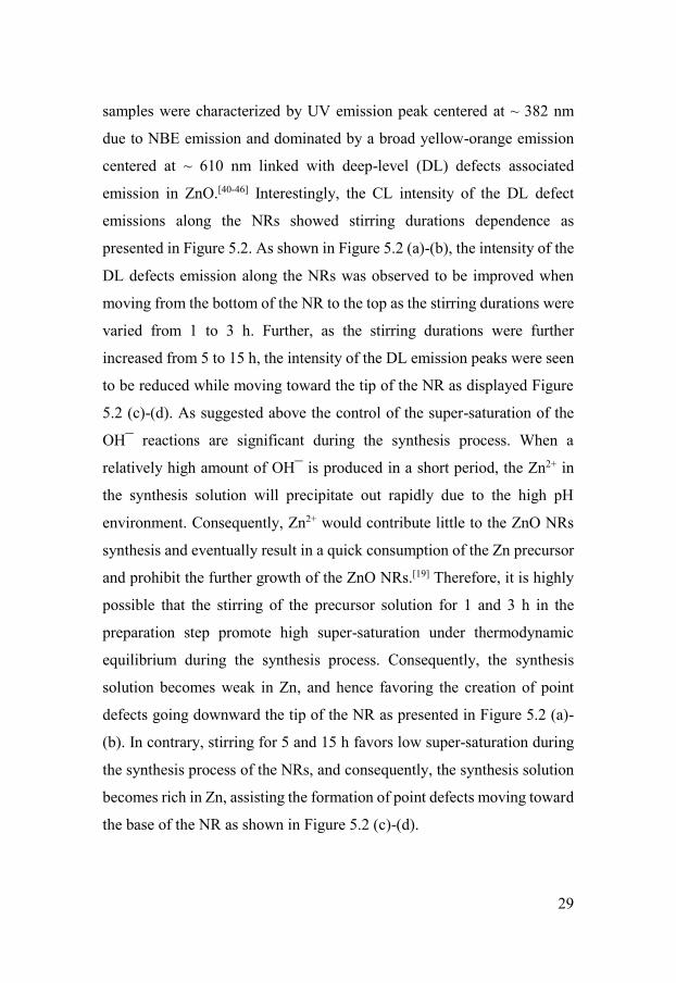
samples were characterized by UV emission peak centered at ~ 382 nm
due to NBE emission and dominated by a broad yellow-orange emission
centered at ~ 610 nm linked with deep-level (DL) defects associated
emission in ZnO.[40-46] Interestingly, the CL intensity of the DL defect
emissions along the NRs showed stirring durations dependence as
presented in Figure 5.2. As shown in Figure 5.2 (a)-(b), the intensity of the
DL defects emission along the NRs was observed to be improved when
moving from the bottom of the NR to the top as the stirring durations were
varied from 1 to 3 h. Further, as the stirring durations were further
increased from 5 to 15 h, the intensity of the DL emission peaks were seen
to be reduced while moving toward the tip of the NR as displayed Figure
5.2 (c)-(d). As suggested above the control of the super-saturation of the
OH¯ reactions are significant during the synthesis process. When a
relatively high amount of OH¯ is produced in a short period, the Zn2+ in
the synthesis solution will precipitate out rapidly due to the high pH
environment. Consequently, Zn2+ would contribute little to the ZnO NRs
synthesis and eventually result in a quick consumption of the Zn precursor
and prohibit the further growth of the ZnO NRs.[19] Therefore, it is highly
possible that the stirring of the precursor solution for 1 and 3 h in the
preparation step promote high super-saturation under thermodynamic
equilibrium during the synthesis process. Consequently, the synthesis
solution becomes weak in Zn, and hence favoring the creation of point
defects going downward the tip of the NR as presented in Figure 5.2 (a)-
(b). In contrary, stirring for 5 and 15 h favors low super-saturation during
the synthesis process of the NRs, and consequently, the synthesis solution
becomes rich in Zn, assisting the formation of point defects moving toward
the base of the NR as shown in Figure 5.2 (c)-(d).

30
The phenomenon of the altered CL intensity with the stirring
durations can be explained using results of first-principle density
functional theory calculations, the formation energy of the point defects in
semiconductors depend on the synthesis conditions. In zinc-rich
conditions, VO has lower formation energy than zinc interstitial (Zni)[30,31],
which is most probably the case in our low-temperature aqueous solution
synthesis because the O comes from the super-saturation of the OH¯
reactions, while the zinc nitrate provides the Zn in the solution.[35] The
point defects in our synthesized ZnO NRs are most likely to be VO and Oi.
Figure 5.2: CL spectra of the individual NRs measured in cross-sectional
view. The insets display the cross-sectional SEM images of the NRs with a
sign of the spots where the CL spectra were recorded. For clarity, the
spectra have been subjected to an offset in the vertical direction.

31
5.2 Influence of the ZnO seed layer precursor molar ratios on the
emission properties of n-ZnO NRs-based heterojunction LEDs
ZnO NRs are regarded as one of the most promising candidates for
the development of intrinsic white-LEDs.[22] However, due to the lack of a
method of synthesizing reproducible and stable p-type ZnO, an alternative
procedure is employed to synthesize n-type ZnO NRs on a p-type substrate
e.g., GaN to achieve ZnO NRs-based heterojunction LEDs.[80-87] However,
the LEDs based on this configuration usually show low EL response as a
result of high density of defects and different energy barriers for electrons
and holes at the heterojunction interface.[87] It is known that the interface
defect states can act as non-radiative centers that will drastically diminish
the efficiency of ZnO-based heterojunction LEDs.[85,86] Previously, it has
been indicated that the type of the seed layer utilized in the synthesis of the
ZnO NRs can significantly modify the density of such interface defects,
and so different color emissions can be observed.[63-65] This is because the
seed layer typically exists at the interfaces between the p-GaN substrate
and the synthesized n-ZnO NRs. Consequently, manipulating the ZnO seed
layer synthesis can be a simple and a useful path to tune the defects density
at the n-ZnO NRs/p-GaN interfaces. In this regard, we demonstrate the
possibility to tune the density of defects at the n-ZnO NRs/p-GaN interface
by utilizing ZnO seed layer prepared with different molar ratios.[57] The
influence of the seed layer molar ratios on the density of defects of the
synthesized n-ZnO NRs/p-GaN heterostructure interfaces was studied by
employing spatially resolved CL spectroscopy. Interestingly, the CL
results showed that the seed layer molar ratios have a notable effect on the
concentration of defects at the n-ZnO NRs/p-GaN heterostructure
interface. As can be seen, the synthesized n-ZnO NRs/p-GaN
heterostructure obtained from a seed layer produced with a molar ratio of

32
1:3 M as shown in Figure 5.3 (b) has a high defect emission (and
consequently high defects concentrations) at the interface (red curve).[57]
Figure 5.3: CL spectra of n-ZnO NRs/p-GaN heterostructure recorded in
cross-sectional view. The inset displays a typical cross-sectional SEM
image of the n-ZnO NRs/p-GaN heterostructure with the sign of the point
where the CL spectra were recorded.
Moreover, to study the impact of the seed layer molar ratios on the
EL emission, the synthesized n-ZnO NRs/p-GaN heterostructures were
used to fabricate LED devices. The fabricated heterojunction LEDs were
marked as device 1, 3, and 5 for the ZnO NRs obtained using a molar ratio
of 1:1, 1:3, and 1:5 M, respectively. Figure 5.4 (a)-(c) present the EL
spectra from all the three LED devices monitored at varying the forward
voltage/injection-currents. As can be observed, the EL spectra of all the
three devices show a distinct yellow emission peak centered at ~575 nm,
which can be ascribed to intrinsic DL defects emission in ZnO due to point
defects e.g., VO and Oi or be interpreted by the interface defects related
emission.[82-85,88-91] In addition to the yellow emission, a weak blue
emission centered at ~ 420 nm was observed for device 1 (with a 1:1 M
seed layer) as presented in Figure 5.4 (a). This observation can be attributed
to the transitions from the CB or shallow donors (in ZnO) to the Mg
acceptor levels in the p-GaN.[83,85]

33
Figure 5.4: EL spectra as a function of the forward bias voltage of device
(a) 1, (b) 3, and (c) 5, respectively. The insets present the corresponding
light emission images at 24 V. (d) The integrated EL intensities of the three
devices as a function of the forward bias voltage.
As the bias voltage is increased, the EL intensity of the dominant
emission peak for all the three LEDs increases rapidly without a notable
shift in the peak position as displayed in Figure 5.4 (d). The increase in the
EL intensity with increasing the bias voltage is probably due to the
reduction in the band bending of the n-ZnO NRs and the p-GaN. Therefore,
the kinetic energy of the electrons and holes is increased, and they have a
much higher probability to flow across the interface barrier and recombine
on the opposite side of the junction.[85,92]

34
Furthermore, the explanation of the mechanism of the enhanced EL
intensity of the yellow emission from the fabricated heterostructure LEDs
is given below. The integrated EL peak intensity as a function of the
injection current is plotted on a log-log scale as shown in Figure 5.5 for all
the three LEDs. The results can be fitted with the law L = cIm, where m
measures the impact of the non-radiative defects in the characteristics of
the light emission. A linear rise in L with I e.g., m ~1 can be assumed when
radiative recombination dominates, while non-radiative recombinations
become dominant when L displays a super-linear dependence on the I e.g.,
when m >1.[93,94] Our result revealed a super-linear dependence with m =
2.3, 4.0, and 1.9 for devices 1, 3, and 5, respectively. These values indicate
the role of the defect-related non-radiative recombination centers for all the
three LEDs, which is in good agreement with the CL spectra in Figure 5.3.
However, the value of m is defined from the fitting curve for device 5 (with
1:5 M) is the lowest (m = 1.9), which shows a low presence of non-radiative
recombination centers in the space-charge region. Since the low density of
the interface defects is favorable for improving carrier injection through
the heterojunction, device 5 shows an improved EL performance compared
to the other two devices 1 and 3. These results suggest that the molar ratios
of the ZnO seed layer have a significant effect on the density of interface
defects and, in particular, playing a role of non-radiative recombination
centers.

35
Figure 5.5: Integrated EL peak intensities of all the three devices as a
function of the forward injection current. The solid lines represent the
fitting results based on the power law L= cIm .
5.3 Influence of ZnO seed layer precursor types on the emission
properties of n-ZnO NRs-based heterojunction LEDs
Proceeding with the investigation of the effect of the ZnO seed layer
on the emission properties of n-ZnO NRs-based heterojunction LEDs and
by choosing the best-optimized seed layer molar ratio. We further studied
the influence of the seed layer precursor types on the emission properties
of n-ZnO NRs-based heterojunction LEDs.[58] Figure 5.6 (a) displays the
top-view CL spectra of the synthesized n-ZnO NRs/p-GaN
heterostructures, which is described by a weak NBE emission peak
centered at ~ 383 nm and a dominant a yellow–orange peak centered at ~
610 nm related to DL defects emission.[82,85,88-91] The yellow–orange
emission is usually observed in the ZnO NRs synthesized by the LT-ACS,
and it is stated to be due to DL defects emission e.g., VO and Oi in ZnO or
can be caused by the VZn and hydrogen complex defects.[20] As can be
observed from Figure 5.6 (a) the synthesized n-ZnO NRs/p-GaN NRs
heterostructure obtained from a seed layer prepared from ZnAc, KOH and

36
HMTA (donated as ZKH seed) displayed good crystal quality and low
defects concentrations compared to that prepared from ZnAc and KOH
(donated as ZK seed), as deduced from the ratio of the NBE to DL defect
emission.[63] Moreover, as revealed by spatially resolved CL, the
synthesized n-ZnO NRs/ p-GaN heterostructure using the ZKH seed layer
shows a significant reduction in the interface defects as illustrated in figure
5.6 (b). This decrease in the CL intensity of the defects emission is likely
to be due to the different defects concentrations at the interface between
the two types of the ZnO NRs/p-GaN heterostructures e.g., higher for ZnO
NRs achieved using the ZK seed solution.[57]
Figure 5.6: (a) CL spectra of the n-ZnO NRs/ p-GaN heterostructures
recorded in top-view mode. For clarity, all the spectra are normalized to
the DL defects emission and shifted in the vertical direction. (b) Cross-
sectional view CL spectra of the n-ZnO NRs/p-GaN heterostructures
interface. The insets display the synthesized n-ZnO NRs/p-GaN
heterostructures in cross-sectional view with a sign of the points where the
CL spectra were measured.
Further, the EL of the fabricated LED devices was performed at
different bias voltages to understand the evolution and tuning of the
emission through the ZnO seed layer precursors, as displayed in Figure 5.7

37
(a)-(b). The EL intensity of the dominant emission peak increases rapidly
without a notable shift in the peak position with increasing the bias voltage.
The dominant broad yellow emission has a slightly asymmetric shape and
therefore can consists of several DL defects emission transitions levels.
Figure 5.7 (c) displays an example of the peak decomposition applying a
Gaussian function for the experimental spectrum performed at a bias
voltage of 15V for the ZKH device, which shows that the dominant broad
emission peak consists of three separate visible defect emission bands
centered at ~ 551, 597, and 652 nm, respectively. These visible defects
emission is probably due to transitions from the CB to DL defects emission
induced by VO and Oi in the ZnO [57,82,85,94] or could be due to radiative
interface recombinations within the n-ZnO NRs and the p-GaN
substrate.[63,64] The difference in the emission spectra of the ZH device and
the ZHK device in Figure 5.7 (d) can be explained by the difference in the
density of interface point defects as indicated in Figure 5.6 (b).
Consequently, the band alignment in the n-ZnO NRs/p-GaN is predicted
to be different, and hence a variation in carrier recombination can be
observed.[63]
An apparent increase in the EL intensity of the dominant emission
peak for the two LEDs is seen as the bias voltage is increased as displayed
in Figure 5.8 (a). The improvement in the EL intensity with increasing the
bias voltage is probably due to the lowering of the band bending of the n-
ZnO NRs and the p-GaN [85,93]. As a result, the kinetic energy of the
electrons and holes is increased, and they have a much higher chance to go
across the interface barrier and recombine on the opposite the side of the
heterojunction.[82,85,93]

38
Figure 5.7: EL spectra of (a) ZK device, and (b) ZKH device, as a function
of the bias voltage. The insets show the corresponding light emission
images at 15 V. (c) Gaussian decomposition of the dominant yellow
emission of the ZKH device at a bias voltage of 15 V. (d) EL spectra of the
two devices under a bias voltage of 15 V.
Further, the integrated intensity of the EL peak as a function of the
injection current is plotted on a log-log scale as shown in Figure 5.8 (b) to
illustrate the mechanism of the improved EL from the fabricated ZKH
LEDs. The curve fitting results exhibited a super-linear dependence with n
= 2.0 for the ZK and 1.3 for the ZKH device, respectively (as deduced from
L = CIn) [93], which suggests that the role of the defect-related non-radiative
recombination centers is dominant for all the two LEDs. However, the
value of n (1.3) for the ZKH device indicates a comparatively lower
existence of non-radiative recombination centers in the space-charge
region. Since the low concentration of interface defects is convenient and

39
is a benefit for carrier injection through the heterojunction. The ZKH
device displayed an enhanced EL performance in contrast to the ZK device
as shown in Figure 5.7 (d). These results imply that the ZnO seed layer
precursor has a significant effect on the interface defect properties and
precisely it is playing an important role in the concentration of the non-
radiative recombination centers.
Figure 5.8: (a) The integrated EL peak intensities of the ZH and ZKH
devices as a function of the bias voltage, and (b) Role of injection current.
The solid lines in Figure b illustrate the fitting results based on the power
law L= CIn.
5.4 Synthesis of Co-doped ZnO oriented NRs
Doping is a prime method to tune the semiconductor properties e.g.,
optical, electronic and magnetic. Recently, theoretical predictions and
experimental research have established that the incorporation of TMs e.g.,
iron (Fe), nickel (Ni), manganese (Mn), cobalt (Co), and copper (Cu) in
ZnO will result in a potential for the development of RT-FM.[47-50] Among
a variety of TMs-doped ZnO, Co is of particular interest because it has
unique optical and magnetic properties.[51,52,95-98] Consequently, substantial
research efforts have been devoted to synthesize Co-doped ZnO utilizing
different synthesis methods. Most of this research has been concentrated

40
on investigating the optical and magnetic properties of Co-doped ZnO.[48-
51] However, the synthesis of a high crystal quality of Co-doped ZnO with
the successful substitution of Co2+ in the host crystal site is still
challenging. The successful realization of high crystal quality Co-doped
ZnO will probably lead to better understanding of the origin of the RT-FM
in ZnO. In particular, doping of Co ions in ZnO crystal lattice utilizing the
low-temperature solution process can be challenging because the dopant
species can easily create aquo ions and not incorporated in the crystal
lattice.[39] Here, by developing a process for preparing the synthesis
solution, we synthesized well-oriented Co-doped ZnO NRs, and the crystal
structure was studied at low-temperature using EPR.[52] Figure 5.9 presents
a top-view SEM images of the synthesized pure (S0) and 5% Co-doped
ZnO NRs (S2) samples, which have a characteristic length of 3.5 μm and
mean diameters of 220 and 300 nm, respectively.
Figure 5.9: Top-view SEM images of the pure (S0) and 5% Co-doped
ZnO NRs (S2), respectively.
The EPR spectra of the pure sample (S0) are defined by the well-
known defect signal from ZnO apparent at 350 mT (g ~ 1.956) as displayed
in Figure 5.10, and usually, assigned to core-defects (CDs) resulting from
ZnO NSs rather than shell defects.[99-101] This g (~1.96) CD signal is
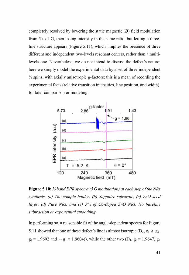
41
completely resolved by lowering the static magnetic (B) field modulation
from 5 to 1 G, then losing intensity in the same ratio, but letting a three-
line structure appears (Figure 5.11), which implies the presence of three
different and independent two-levels resonant centers, rather than a multi-
levels one. Nevertheless, we do not intend to discuss the defect’s nature;
here we simply model the experimental data by a set of three independent
½ spins, with axially anisotropic g-factors: this is a mean of recording the
experimental facts (relative transition intensities, line position, and width),
for later comparison or modeling.
Figure 5.10: X-band EPR spectra (5 G modulation) at each step of the NRs
synthesis. (a) The sample holder, (b) Sapphire substrate, (c) ZnO seed
layer, (d) Pure NRs, and (e) 5% of Co-doped ZnO NRs. No baseline
subtraction or exponential smoothing.
In performing so, a reasonable fit of the angle-dependent spectra for Figure
5.11 showed that one of these defect’s line is almost isotropic (D3, g g,
g = 1.9602 and ~ g = 1.9604)), while the other two (D1, g = 1.9647, g

42
= 1.9630, and D2, g = 1.9619, g = 1.9607) display a slight axial
anisotropy, in consistency with the hexagonal wurtzite structure of the ZnO
NRs.[52] The observation of this anisotropy is a first evidence that the NRs
are single crystalline and are mostly vertically oriented. We summarize the
pure NRs under study by noting that their EPR signals are well identified.
They contain known ZnO CDs and were mostly aligned perpendicularly to
the substrate surface, and no detectable traces of defects or impurities are
observed, a fact which indicates the relatively high purity of these samples.
Figure 5.11: Experimental X-band EPR spectra (1G modulation) of
sample S0 showing the g ~ 1.96 signal for B // z (θ = 0º) and B z (θ =
90º), recorded at T = 5 K. The upper x-axis gives the corresponding g
factor value.
The EPR spectra of the 5% Co-doped NRs (samples S2), is
significantly characterized by a reduction of the CDs signal (g ~ 1.96)
intensity which is observed in S0 ( Figure 5.10) and the appearance of a
Co-related signal at g ~ 2.24, for θ = 0º, and at g ~ 4.58 for θ = 90º as
displayed in Figure 5.12. The observed reduction of the CD is an
interesting sign that a certain amount of the incorporated Co is involved in

43
the neutralization of the CDs. Whereas the observed magnetic anisotropy
of the Co2+ signal is a clear evidence that the NRs are single crystalline and
are vertically well aligned, at least everywhere the Co ions supply an EPR
signal.[52]
Figure 5.12: X-band EPR spectra of sample S2 for parallel (θ = 0º) and
perpendicular (θ = 90º) orientation of the B field. The CD and sample
holder (SH) signals are indicated. Gravity centers of the Co2+ signal for
both orientations are indicated.
5.5 The influence of the synthesis solution mixing on Co-doped ZnO
NRs
To confirm our approach for the synthesis of high crystal quality
Co-doped ZnO NRs using the LT-ACS route, we further examined the
effect of the mixing the synthesis solution on the substitution of Co ions in
the ZnO crystal lattice while preserving the NRs morphology and
alignment. In general, the synthesis of Co-doped ZnO NRs using the LT-
ACS route is carried out by adding the Co ions source to the already
prepared mixture of the Zn salt with HMTA synthesis solution. Here, in

44
addition to the above method for the synthesis of Co-doped ZnO NRs, we
adapted another way by mixing the HMTA with Co dopant source first and
then adding the Zn salt.[34,52,59]
Figure 5.13 displays a top-view FE-SEM images of the synthesized
pure (M0) and Co-doped ZnO NRs synthesized by mixing Zn salt with
HMTA and then adding Co salt ( labeled as M1), mixing Co salt with
HMTA and then adding Zn salt (labeled as M2). Vertically aligned NRs
with a hexagonal shape and having an average diameter of ~160, ~400, and
~200 nm for M0 (pure ZnO NRs), M1, and M2, respectively, were obtained
as shown in Figure 5.13. The notable and slight increase in the NRs average
diameter between the M1 and M2 as compared to M0 is possibly due to
the Co doping. [102,103]
Figure 5.13: Top-view FE-SEM images of pure (M0) and Co-doped ZnO
NRs synthesized using approaches M1 and M2, respectively.
The crystal structure quality of the synthesized pure and Co-doped
ZnO NRs has been confirmed by the XRD measurements as illustrated in
Figure 5.14. The XRD patterns showed that all the synthesized samples
had a wurtzite structure with a good crystal quality and preferred growth
orientation along the c-axis, as indicated by the intensity of the (002) peak.
No secondary phase related to Co was seen in the XRD patterns of the pure
and Co-doped ZnO NRs samples. The slight shift in the (002) peak position

45
toward lower 2θ angle in M1 and higher 2θ angle in M2 (as shown in the
inset of Figure 5.14) as compared to M0 is an indication of the successful
incorporation of the Co or the due to the difference of defects density in
the synthesized NRs.[103-105]
Figure 5.14: XRD patterns of the synthesized pure (M0) and Co-doped
ZnO NRs (M1 and M2). The inset shows the normalized XRD data for the
(002) peaks, indicating peaks shift.
The effect of the incorporation of Co into the ZnO using the two
different methods (M1 and M2) was investigated using EPR
measurements. The successful substitution of Co2+ was confirmed by the
observed Co-related signal defined by an eight-line structure at g ~ 2.239
(θ = 0º) and a broad asymmetric signal at g ~ 4.517 (θ = 90º) [51,52] as
displayed in Figure 5.15. The detected magnetic anisotropy of the Co2+
signal is clear evidence that the synthesized ZnO NRs are single crystalline,
well-aligned, and that Co is highly diluted along the NRs.[36]
As presented in Figure 5.15, the intensity of the Co2+ signal of M2
at θ = 90º and θ = 0º is significantly higher as compared to that of M1.
Also, the line width of the Co2+ signal at θ = 0º for M2 is observed to be

46
slightly smaller (4G) than that of M1 (5G). As the Co concentration in the
synthesis solution is the same (7%) for both M1 and M2, and by
considering a uniform doping and the same coverage of the NRs, these
results reveal that the way of preparing the synthesis solution has a
significant influence on the Co incorporation in the synthesized ZnO NRs
in agreement with the XRD results displayed in Figure 5.14.
Figure 5.15: EPR spectra of Co-doped ZnO NRs (M1 and M2) for parallel
(θ = 0º) and perpendicular (θ = 90º) orientation of the magnetic field,
recorded at T = 5 K.
Moreover, to get more information on the defects in the synthesized
pure and Co-doped ZnO NRs, measurement and analysis of the room-
temperature CL spectra were carried out, and the results are presented in
Figure 5.16. The emission spectra of all samples were dominated by a UV
emission peak centered at ~ 382 nm (3.24 eV) due to NBE emission and
strong broad yellow-orange emission centered at ~ 610 nm (2.03 eV)
connected with the DL defects associated emissions in ZnO.[46,105]
Apparently, the CL spectra of the Co-doped ZnO NRs displayed a small
red-shift of the UV peak position from 382 nm to 384 nm (as displayed in

47
the inset of Figure 5.16) as compared to pure ZnO NRs, which is likely to
be due to the change in band structure as a result of Co doping.[102,105] It is
important to note that the CL defect-related yellow-orange emission
intensity decrease from M1 to M2 (Figure. 5.16), and the Co EPR signal
increases from M1 to M2 (Figure 5.15). These observations propose that
the method of preparing the synthesis solution has a substantial impact on
the Co incorporation and defect generation in the synthesized ZnO NRs in
agreement with the XRD results shown in Figure 5.14. The physical source
of intrinsic defects-related yellow-orange emission is doubtful, and it is
stated to be linked to the Vo, Oi, and Zni. Recently, it was suggested that
the defect-related orange emission is to possibly be originating due to the
Zni in the core of ZnO NRs.[106]
Figure 5.16: CL spectra of the synthesized pure and Co-doped ZnO NRs
obtained by utilizing different synthesis preparation approaches as
indicated. The inset demonstrates the red-shift in the UV peak. For clarify,
the spectra are normalized to the NBE intensity.

48
In this study, we suggest that the defect-related yellow-orange
emission is likely to originate from Zni in the core of ZnO NRs or from the
Vo and Oi on the surface of ZnO NRs. As a result, the intensity of the
defect-related yellow-orange emission is significantly improved by the Co-
doping (Figure 5.16), which is presumably due to the increase in Vo and
Oi in the NRs or to the Co-related defect.[15,23,41] This suggests that the
above-observed red-shift of the UV peak could be ascribed to the variation
of the Zni concentrations in the Co-doped samples (M1 and M2) compared
with the pure ZnO NRs (M0). In fact, these results indicate that the bulk
quality of the ZnO NRs is improved by the substitution of Co2+, while the
doping has the adverse effect on the surface defects-related emission, in
agreement with early results.[105,107]
In view of the EPR and the CL results, a defect distribution model
for ZnO NRs is proposed as shown in Figure 5.17[108], which states that the
incorporation of Co2+ during the synthesis process could reasonably result
in filling Zni+ by substitutional or interstitial doping and, consequently,
improved the crystal quality of the synthesized ZnO NRs.[51] The other
possibility is that a substitutional Co2+ very close to a Zni+ may form a non-
magnetic complex, which is then not anymore EPR detectable.
Figure 5.17: Schematic diagram of the cross-sectional view of the
synthesized pure and Co-doped ZnO NRs including Zni+ as core-defect and
oxygen vacancies/interstitials as surface defects, respectively.

49
Moreover, the incorporation of Co2+ was observed to lead to the
increased concentration of surface defects such as VO and Oi. However,
further experimental investigation coupled with comprehensive theoretical
calculations are required to fully understand this observed phenomena.
5.6 Core-defect reduction in ZnO NRs by Co incorporation
As mentioned previously, ZnO NRs have a potential for the
development of a diverse range of functional electronic devices e.g., LEDs [22] and UV detectors.[25-27] In these applications, intrinsic and extrinsic
defects play a significant role in their optical and electrical properties.
Consequently, information about and control of these defects, as well as
the relation between them, are essential factors for the optimization of the
electronic and optical properties of ZnO NRs. In particular, the
paramagnetic defects are of interest because when an externally applied
magnetic field, the majority of electrons (depending on temperature) have
up (or down) spin projection, which then restricts the possible
recombination paths via these polarized defects to those allowed by Pauli
exclusion principle. Regarding these paramagnetic defects, the EPR is a
valuable tool to characterize them and to examine their occurrence as a
function of the different synthesis parameters.[34,52,77] Simultaneously, the
EPR spectra can give information about the spin environment, the crystal
quality at the atomic scale, and the macroscopic ordering. However,
applying the EPR spectroscopy on paramagnetic NSs is tricky, mainly due
to the moderate amount of resonating centers and the large spin relaxation.
Moreover, as most of the previous studies deal with non-oriented NPs,
information on magnetic anisotropy is often lost. Therefore, here we
synthesized well-oriented pure and Co-doped ZnO NRs by the LT-ACS
(90 °C) with different Co concentrations within the synthesis solution

50
(from 0% to 15%), and are investigated by the EPR, just above the liquid
helium temperature. The analysis of the EPR spectra shows that a decrease
in the intensity of the paramagnetic native CD at g ~1.96 with the increase
of Co in the synthesis solution, proposing a gradual neutralization of the
former by the latter as presented in Figure 5.18. However, the comparison
of absolute intensity in different samples does not lead to significant
information since the total number of the NRs may vary from a sample to
another, mainly due to the differences in the substrate coverage.
Figure 5.18: Evolution of the CDs signal with the Co concentration within
the synthesis solution. The line of the 0% is divided by 100.
To explain the gradual decrease of the CDs single with the increase
of Co in the synthesis solution, three main interpretations are possible:
firstly, the presence of Co in the synthesis solution may directly inhibit the
formation of this CD during the growth. Secondly, the paramagnetic
incorporated Co2+ ions and CD may form a non-magnetic complex, which
is then not detectable by the EPR, and finally, another type of non-magnetic

51
incorporated Co may break down the CD, for instance by filling a vacancy.
It has also been proposed that the disappearance of the g ~ 1.96 signal when
the TMs ions are incorporated in ZnO can only be due to the significant
broadening due to spin-spin relaxation with the 3d electrons. However, it
is difficult to imagine Co2+ ions interacting with a CD without being altered
in its magnetic parameters so that, as only Co2+ ions with bulk parameters
are detected, this proposal may be finally equivalent to the second
explanation.[34]
The physics of ZnO intrinsic and extrinsic defects are so plentiful
that many types of defects complexes are likely to take place. Regarding
our samples, we first note that in all of them, except the g ~ 1.96 CD signal,
no other defect or pollution-related lines are detected, indicating to the high
crystal quality and purity of the NRs under investigation. The CD signal
detected on the pure ZnO NRs (0% Co)as shown in Figure 5.19 is made of
at least two close lines, which collapse into a single asymmetric line for θ
= 90. Here, one of these observed lines appears to be almost isotropic (g
g), while the other one displays a slight easy-axis anisotropy (g g)
signed by the displacement of the positive peak. This shift allows us to
estimate g (g = g − g) for the anisotropic line to be − 0.0014, thus
likely to be related to a Zni+ defect (g = -0.0010) within the ordered phase
of NRs. Regarding the isotropic line, although an isotropic defect cannot
be excluded, it is likely to be related to the disordered phase present in the
Co-doped samples. If so, the line may arise from a powder of the
anisotropic defect, with slightly modified parameters: this could be the case
for disordered Co-doped ZnO large nanoparticles or partially grown NRs.
Consequently, at this stage, we cannot decide an exact answer to this
question. In particular, because the precise origin of the CDs is not known
with certainty. Further experimental and theoretical investigations have to

52
be performed. For example, ab initio theoretical study of ZnO supercells
containing different types of paramagnetic defects (compatible with slight
easy axis magnetic anisotropy observed in this work) and substitutional
Co2+ ions in various relative positions would give more insight into
answering these questions. We show that only a little amount of Co in the
synthesis solution (about 0.2%) is necessary to suppress almost all these
paramagnetic CDs.[34] These results give insight in the experimentally
observed improvement of the crystal quality of diluted Co-doped ZnO
NRs, as well as into the control of paramagnetic defects in ZnO NRs.
Figure 5.19: Anisotropy of the EPR CD signal in pure (0% Co) and Co-
doped (0.5%) samples, with respect to the magnetic field orientation,
recorded at T=6 K. Sapphire defect (SD) signal present in the 0.5% sample
is shown for the θ=0 orientation.

53
6. Research summary and future work
Zinc oxide (ZnO) nanorods (NRs) exhibit unique optical and
electronic properties, which are of particular interest in the development of
optoelectronic devices e.g., ultraviolet (UV) photodetectors, light-emitting
diodes (LEDs) and solar cells. In addition to this ZnO is a piezoelectric and
biocompatible material. The potential of ZnO NRs in all applications
mentioned above, however, would require synthesis of high crystal quality
with in-depth knowledge in understanding their optical and electronic
properties. As the low-temperature aqueous chemical synthesis (LT-ACS)
holds great promise for the synthesis of ZnO NRs and offers the possibility
to tune their final properties by adjusting the synthesis parameters, intense
research efforts are devoted in this respect. In this regard, vertically well-
aligned ZnO NRs with optimized point defects concentration and
knowledge about their spatial distribution along the NRs were achieved.
Also, high crystal quality well-oriented Co-doped ZnO NRs were obtained
in this thesis. In paper I, by varying the stirring durations for the synthesis
solutions, we were able to tune the defects emission along the NRs, and
this is most likely attributed to the variation of OH¯ concentration during
the growth process by either high or low super-saturations. Then, by
choosing the best stirring duration regarding the vertical alignment and
concentration of defects achieved in the paper I, combined with ZnO seed
layer precursor’s types, and its molar ratios are studied in papers II and III,
and we tuned the concentration of interface defects at the synthesized n-
ZnO NRs/p-GaN heterostructured interface. A significant improvement in
the electroluminescence (EL) intensity was observed for the fabricated
heterojunction LEDs based on the results of papers II and III. The
improved EL intensity from the n-ZnO NRs-based heterojunction LEDs
was likely attributed to reduced density of non-radiative related defect
54
using an optimized molar ratio and a specific precursor type utilized for
the ZnO seed layer. After that, in papers IV-VI, high crystal quality
vertically well-oriented ZnO NRs has been demonstrated by incorporating
diluted cobalt (Co) inside the ZnO NRs crystal lattice. Finally, a
concentration study (paper VI) of the synthesized vertically well-aligned
pure and Co-doped ZnO NRs at low-temperature suggested that a
relatively small amount of Co2+ (0.2 %) is sufficient to suppress almost all
core-defects (CDs) that were observed in pure ZnO NRs. In view of the
different results from all the complementary measurements on the
synthesized pure and Co-doped ZnO NRs, we can summarize that: the
substitution of the Co2+ inside the ZnO NRs supplies a highly anisotropic
magnetic Co2+ signal defined by eight-lines suggesting that the synthesized
NRs are single crystalline, vertically well-aligned, and at least the Co is
homogeneously distributed along the NRs. Also, the substitution of the
Co2+ was observed to be identified by a drastic reduction in the CDs signal
(g ~1.956) seen in pure ZnO NRs. This decrease in the CDs signal is
presumably due to the presence of Co in the synthesis solution may
instantly hinder the formation of these CDs during the growth process.
Another probability is that the paramagnetic incorporated Co2+ ions and
CD may create a non-magnetic complex, which is not detectable by
electron paramagnetic resonance (EPR), or a different type of non-
magnetic incorporated Co might break down the CD, for example by filling
a vacancy. Moreover, the EPR result indicates that the resolved anisotropy
of the CD signal at g ~ 1.96 in pure NRs highly proposes that CD arise, at
least partially, from the Zni+ shallow donor from the core of the NRs rather
than the shell.
Despite tremendous effort devoted to synthesizing high crystalline
quality vertically well-oriented Co-doped ZnO NRs using the LT-ACS,

55
there are many challenges to overcome. For instance, more experimental
research work is needed in adjusting the synthesis parameters to improve
the incorporated amount of the Co2+ ions into the ZnO NRs crystal lattice
while keeping control over the crystal quality, morphology, and
orientations. This step will probably lead to the possible observation of
room-temperature ferromagnetism (RT-FM) from the LT-ACS
synthesized Co-doped ZnO NRs. Further, advanced spectroscopy
investigations e.g., photoluminescence excitation (PLE) and optically
detected magnetic resonance (ODMR) performed at low-temperature and
supported by ab initio theoretical study of ZnO super-cells containing
various types of paramagnetic defects and substitutional Co2+ ions in
different relative positions would give insights into the origin of the CDs.
Furthermore, the potential of the synthesis of optimized Co-doped ZnO
NRs for spintronic-based devices e.g., UV photodetectors, LEDs, and
magnetic capacitors can be utilized.

56

57
7. References
[1] H. S. Nalwa, Handbook of Nanostructured Materials and Nanotechnology, Academic Press, New York, (2000).
[2] C. N. R. Rao, A. Mueller, and A. K. Cheetham, The Chemistry of Nanomaterials: Synthesis, Properties, and Applications, Wiley-VCH, Weinheim, (2004).
[3] G. Cao and Y. Wang, Nanostructures and Nanomaterials: Synthesis, Properties and Applications, World Scientific Publishing Co. Pte. Ltd., Singapore (2011).
[4] O. I. Micic, C. J. Curtis, K. M. Jones, J. R. Sprague, and A. J. Nozik, Synthesis and Characterization of InP Quantum Dots, J. Phys. Chem. 98, 4966 (1994).
[5] T. S. Ahmadi, Z. L. Wang, T. C. Green, A. Henglein, and M. A. El-Sayed, Shape-Controlled Synthesis of Colloidal Platinum Nanoparticles, Science 272, 1924 (1996).
[6] Y. Sun, and Y. Xia, Shape-Controlled Synthesis of Gold and Silver Nanoparticles, Science 298, 2176 (2002).
[7] W. K. Bae, K. Char, H. Hur, and S. Lee, Single-Step Synthesis of Quantum Dots with Chemical Composition Gradients, Chem. Mater. 20, 531 (2008).
[8] C. Wang, H. Daimon, T. Onodera, T. Koda, and S. Sun, A General Approach to the Size and Shape-Controlled Synthesis of Platinum Nanoparticles and Their Catalytic Reduction of Oxygen, Angew. Chem. 47, 3588 (2008).
[9] L. Vayssieres, Growth of Arrayed Nanorods and Nanowires of ZnO from Aqueous Solutions, Adv. Mater. 15, 464 (2003).
[10] Y. Xia, P. Yang, Y. Sun, Y. Wu, B. Mayers, B. Gates, Y. Yin, F. Kim, and H. Yan, One-Dimensional Nanostructures: Synthesis, Characterization, and Applications, Adv. Mater. 15, 353 (2003).
[11] A. Gole, and C. J. Murphy, Seed-Mediated Synthesis of Gold Nanorods: Role of the Size and Nature of the Seed, Chem. Mater. 16, 3633 (2004).
[12] A. K. Geim, and K. S. Novoselov, The rise of graphene, Nat. Mater. 6, 183 (2007).

58
[13] Y. Wu, P. Qiao, T. Chong, and Z. Shen, Carbon Nanowalls Grown by Microwave Plasma Enhanced Chemical Vapor Deposition, Adv. Mater. 14, 64 (2002).
[14] M.-S. Wu, Y.-H. Ou, and Y.-P. Lin, Iron Oxide Nanosheets and Nanoparticles Synthesized by a Facile Single-Step Coprecipitation Method for Lithium-Ion Batteries, Journal of The Electrochemical Society 158 (3), A231 (2011).
[15] B. Cao, W. Cai, Y. Li, F. Sun, and Z. L. Wang, Ultraviolet-light-emitting ZnO nanosheets prepared by a chemical bath deposition method, Nanotechnology 16, 1734 (2005).
[16] Z. R. Tian, J. A. Voigt, J. Liu, B. Mckenzie, M. J. Mcdermott, M. A. Rodriguez, H. Konishi, and H. Xu, Complex and oriented ZnO nanostructures, Nat. Mater. 2, 821 (2003).
[17] Z. L. Wang, Nanostructures of zinc oxide, Mater.Today 7, 26 (2004).
[18] L. E. Greene, M. Law, D. H. Tan, M. Montano, J. Goldberger, G. Somorjai, and P. Yang, General Route to Vertical ZnO Nanowire Arrays Using Textured ZnO Seeds, Nano Lett. 7, 1231 (2005).
[19] S. Xu and Z. L. Wang, One-dimensional ZnO nanostructures: Solution growth and functional properties, Nano Res. 4, 1013 (2011).
[20] U. Özgür, Ya. I. Alivov, C. Liu, A. Teke, M. A. Reshchikov, S. Doğan, V. Avrutin, S.-J. Cho, and H. Morkoç, A comprehensive review of ZnO materials and devices, J. Appl. Phys. 98, 041301 (2005).
[21] C. Klingshirn, ZnO: Material, Physics and Applications, Chem. Phys. Chem. 8, 782 (2007).
[22] M. Willander et al., Zinc oxide nanorod based photonic devices: recent progress in growth, light emitting diodes and lasers, Nanotechnology 20, 332001 (2009).
[23] A. B. Djurišić, A. M. C. Ng, and X. Y. Chen, ZnO nanostructures for optoelectronics: Material properties and device applications, Prog. Quantum Electron. 34, 191 (2010).
[24] Y. Jin, J. Wang, B. Sun, J. C. Blakesley, and N. C. Greenham, Solution-Processed Ultraviolet Photodetectors Based on Colloidal ZnO Nanoparticles, Nano Lett. 8 (6), 1649 (2008).

59
[25] C. Soci, A. Zhang, B. Xiang, S. A. Dayeh, D. P. R. Aplin, J. Park, X. Y. Bao, Y. H. Lo, and D. Wang, ZnO Nanowire UV Photodetectors with High Internal Gain, Nano Lett. 4, 103 (2007).
[26] L. W. Ji, S. M. Peng, Y. K. Su, S. J. Young, C. Z. Wu, and W. B. Cheng, ultraviolet photodetectors based on selectively grown ZnO nanostructures, Appl. Phys. Lett. 94, 203106 (2009).
[27] C. O. Chey, X. Liu, H. Alnoor, O. Nur, and M. Willander, Fast piezoresistive sensor and UV photodetector based on Mn-doped ZnO nanorods, Phys. Status Solidi RRL 9, 87 (2015).
[28] M. Law, L. E. Greene, J. C. Johnson, R. Saykally, and P. Yang, Nanowire dye-sensitized solar cells, Nat. Mater. 4, 455 (2005).
[29] C.-W. Liu, S.-J. Chang, S. Brahma, C.-H. Hsiao, F. M. Chang, P. H. Wang, and K. Y. Lo, Hydrothermally grown oriented ZnO nanorod arrays for gas sensing applications, J. Appl. Phys. 117, 084315 (2015).
[30] F. A. Kohan, G. Ceder, D. Morgan, and C. G. Van De Walle, First-principles study of native point defects in ZnO, Phys. Rev. B 61, 15019 (2000).
[31] C. G. Van De Walle, Defect analysis and engineering in ZnO, Physica B 308–310, 899 (2001).
[32] D. Li, Y. H. Leung, A. B. Djurišić, Z. T. Liu, M. H. Xie, S. L. Shi, S. J. Xu, and W. K. Chan, Different origins of visible luminescence in ZnO nanostructures fabricated by the chemical and evaporation methods, Appl. Phys. Lett. 85, 1601 (2004).
[33] K. H. Tam, C. K. Cheung, Y. H. Leung, A. B. Djurišić, C. C. Ling, C. D. Beling, S. Fung, W. M. Kwok, W. K. Chan, D. L. Phillips, L. Ding, and W. K. Ge, Defects in ZnO Nanorods Prepared by a Hydrothermal Method, J. Phys. Chem. B 110, 20865 (2006).
[34] A. Savoyant, H. Alnoor, O. Pilone, O. Nur, and M. Willander, Core-defect reduction in ZnO nanorods by cobalt incorporation, Nanotechnology 28, 285705 (2017).
[35] A. Zainelabdin, S. Zaman, G. Amin, O. Nur, and M. Willander, Deposition of Well-Aligned ZnO Nanorods at 50 °C on Metal, Semiconducting Polymer, and Copper Oxides Substrates and Their Structural and Optical Properties, Cryst. Growth Des. 10, 3250 (2010).

60
[36] M. H. Asif, S. M. U. Ali, O. Nur, M. Willander, C. Brännmark, P. Strålfors, U. H. Englund, F. Elinder, and B. Danielsson, Functionalised ZnO-nanorod-based selective electrochemical sensor for intracellular glucose, Biosensors and Bioelectronics 25, 2205 (2010).
[37] Z. L. Wang and S. J, Piezoelectric nanogenerators based on zinc oxide nanowire arrays, Science 312, 242 (2006).
[38] A. Kumar, H. Gullapalli, K. Balakrishnan, A. Botello-Mendez, R. Vajtai, M. Terrones, and P. M. Ajayan, Flexible ZnO–Cellulose Nanocomposite for Multisource Energy Conversion, Small 7, 2173 (2011).
[39] L. E. Greene, B. D. Yuhas, M. Law, D. Zitoun, and P. Yang, Solution-Grown Zinc Oxide Nanowires, Inorganic Chemistry 19, 7535 (2006).
[40] L. E. Greene, M. Law, J. Goldberger, F. Kim, J. C. Johnson, Y. Zhang, R. J. Saykally, and P. Yang, Low-Temperature Wafer-Scale Production of ZnO Nanowire Arrays, Angew, Chem. Int.Ed. 42, 3031 (2003).
[41] E. De la Rosa, S. Sepúlveda-Guzman, B. Reeja-Jayan, A. Torres, P. Salas, N. Elizondo, and M. Jose Yacaman, Controlling the Growth and Luminescence Properties of Well-Faceted ZnO Nanorods, J. Phys. Chem. C 111, 8489 (2007).
[42] A. Escobedo-Morales and U. Pal, Defect annihilation and morphological improvement of hydrothermally grown ZnO nanorods by Ga doping, Appl. Phys. Lett. 93, 193120 (2008).
[43] A. B. Djurišić, Y. H. Leung, K. H. Tam, Y. F. Hsu, L. Ding, W. K. Ge, Y. C. Zhong, K. S. Wong, W. K. Chan, H. L. Tam, K.W. Cheah, W. M. Kwok, and D. L. Phillips, Defect emissions in ZnO nanostructures, Nanotechnology 18, 095702 (2007).
[44] A. Zainelabdin, S. Zaman, G. Amin, O. Nur, and M. Willander, Stable White Light Electroluminescence from Highly Flexible Polymer/ZnO Nanorods Hybrid Heterojunction Grown at 50°C, Nanoscale Res Lett. 5, 1442 (2010).
[45] T. M. Børseth, B. G. Svensson, A. Y. Kuznetsov, P. Klason, Q. X. Zhao, and M. Willander, Identification of oxygen and zinc vacancy optical signals in ZnO, Appl. Phys. Lett. 89, 262112 (2006).
61
[46] N. H. Alvi, K. ul Hasan, O. Nur, and M. Willander, The origin of the red emission in n-ZnO nanotubes/p-GaN white light emitting diodes, Nanoscale Res. Lett. 6, 130 (2011).
[47] J. K. Furdyna, Diluted magnetic semiconductors, J. Appl. Phys. 4, 15 (1988).
[48] K. R. Kittilstved, W. K. Liu, and D. R. Gamelin, Electronic structure origins of polarity-dependent high-TC ferromagnetism in oxide-diluted magnetic semiconductors, Nat. Mater. 5, 291 (2006).
[49] P. Sharma, A. Gupta, K. V. Rao, F. J. Owens, R. Sharma, R. Ahuja, J. M. Osorio Guillen, B. Johansson, and G. A. Gehring, Ferromagnetism above room temperature in bulk and transparent thin films of Mn-doped ZnO, Nat. Mater. 2, 673 (2003).
[50] Z. H. Zhang, X. Wang, J. B. Xu, S. Muller, C. Ronning, and Q. Li, Evidence of intrinsic ferromagnetism in individual dilute magnetic semiconducting nanostructures, Nat. Nanotechnology. 4, 523 (2009).
[51] P. Lommens, F. Loncke, P. F. Smet, F. Callens, D. Poelman, H. Vrielinck, and Z. Hens, Dopant Incorporation in Colloidal Quantum Dots: A Case Study on Co2+ Doped ZnO, Chem. Mater. 19, 5576 (2007).
[52] A. Savoyant, H. Alnoor, S. Bertaina, O. Nur, and M. Willander, EPR investigation of pure and Co-doped ZnO oriented nanocrystals, Nanotechnology 28, 035705 (2017).
[53] K. Govender, S. D. Boyle, B. P. Kenway, and P. O’Brien, Understanding the factors that govern the deposition and morphology of thin films of ZnO from aqueous solution, J. Mater. Chem 14, 2575 (2004).
[54] S. Xu, C. Lao, B. Weintraub, and Z. L. Wang, Density-controlled growth of aligned ZnO nanowire arrays by seedless chemical approach on smooth surfaces, J. Mater. Res. 23, 2072 (2008).
[55] Y. Zhang, M. K. Ram, E. K. Stefanakos, and D. Y. Goswami, Synthesis, Characterization, and Applications of ZnO Nanowires, J. Nanomater. 2012, 1 (2012).
[56] H. Alnoor, C. O. Chey, G. Pozina, X. Liu, V. Khranovskyy, M. Willander, and O. Nur, Effect of precursor solutions stirring on deep level defects concentration and spatial distribution in low temperature aqueous chemical synthesis of zinc oxide nanorods, AIP Advances 5, 087180 (2015).

62
[57] H. Alnoor, G. Pozina, V. Khranovskyy, X. Liu, D. Iandolo, M. Willander, and O. Nur, Influence of ZnO seed layer precursor molar ratio on the density of interface defects in low temperature aqueous chemically synthesized ZnO nanorods/GaN light-emitting diodes, J. Appl. Phys. 119, 165702 (2016).
[58] H. Alnoor, G. Pozina, M. Willander, and O. Nur, Seed layer synthesis effect on the concentration of interface defects and emission spectra of ZnO nanorods/p-GaN light-emitting diode, Phys. Status Solidi A 214, 1862 (2017).
[59] H. Alnoor, A. Savoyant, X. Liu, G. Pozina, M. Willander, and O. Nur, An effective low-temperature solution synthesis of Co-doped [0001]-oriented ZnO nanorods, J. Appl. Phy. 121, 215102 (2017).
[60] J. Song and S. Lim, Effect of Seed Layer on the Growth of ZnO Nanorods, J. Phys. Chem. C 111, 596 (2007).
[61] L.-W. Ji, S.-M. Peng, J.-S. Wu, W.-S. Shih, C.-Z. Wu, and I-T. Tang, Effect of seed layer on the growth of well-aligned ZnO nanowires, Journal of Physics and Chemistry of Solids 70, 1359 (2009).
[62] S.-W. Chen and J.-M. Wu, Nucleation mechanisms and their influences on characteristics of ZnO nanorod arrays prepared by a hydrothermal method, Acta Mater. 59, 841 (2011).
[63] A. M. C. Ng, X. Y. Chen, F. Fang, Y. F. Hsu, A. B. Djurišić, C. C. Ling, H. L. Tam, K. W. Cheah, P. W. K. Fong, H. F. Lui, C. Surya, and W. K. Chan, Solution-based growth of ZnO nanorods for light-emitting devices: hydrothermal vs. electrodeposition, Appl. Phys. B 100, 851 (2010).
[64] A. M. C. Ng, Y. Y. Xi, Y. F. Hsu, A. B. Djurišić, W. K. Chan, S. Gwo, H. L. Tam, K. W. Cheah, P. W. K. Fong, H. F. Lui, and C. Surya, GaN/ZnO nanorod light emitting diodes with different emission spectra, Nanotechnology 20, 445201 (2009).
[65] X. Y. Chen, A. M. C. Ng, F. Fang, A. B. Djurišić, W. K. Chan, H. L. Tam, K. W. Cheah, P. W. K. Fong, H. F. Lui, and C. Surya, The Influence of the ZnO Seed Layer on the ZnO Nanorod/GaN LEDs, J. Electrochem. Soc. 157 (3), H308 (2010).

63
[66] W. Zhou, R. Apkarian, Z. L. Wang, and D. Joy, Fundamentals of Scanning Electron Microscopy (SEM): Scanning Microscopy for Nanotechnology, Springer New York, 1-40 (2007).
[67] G. Will, Powder Diffraction, Springer Berlin Heidelberg, 1-39 (2006).
[68] J. F. Moulder, W. F. Stickle, P.E.'Sobol, and K. D. Bomben, Handbook of X-ray Photoelectron Spectroscopy, Physical Electronics USA, Inc., (1995).
[69] H.-L. Lee and N. T. Flynn, Handbook of Applied Solid State Spectroscopy, X-RAY PHOTOELECTRON SPECTROSCOPY, 485 (2006).
[70] G. D. Gilliland, photoluminescence spectroscopy of crystalline semiconductors, Mater. Sci. Eng., R. 18, 99 (1997).
[71] B. G. Yacobi and D.B. Holt, Cathodoluminescence Microscopy of inorganic solids, Plenum Press, New York (1990).
[72] A. Gustafsson, M.-E. Pistol, L. Montelius, and L. Samuelson, Local probe techniques for luminescence studies of low-dimensional semiconductor structures, J. Appl. Phys. 84, 1715 (1998).
[73] L. J. Brillson, Applications of depth-resolved cathodoluminescence spectroscopy, J. Phys. D: Appl. Phys., 45, 183001 (2012).
[74] K. Thonke, I. Tischer, M. Hocker, M. Schirra, K. Fujan, M. Wiedenmann, R. Schneider, M. Frey, and M. Feneberg, Nanoscale characterization of semiconductors by cathodoluminescence spectroscopy, IOP Conf. Series: Mater. Sci. Eng., 55, 012018 (2014).
[75] L. J. Brillson, W. T. Ruane, H. Gao, Y. Zhang, J. Luo, H. von Wenckstern, and M. Grundmann, Spatially-resolved cathodoluminescence spectroscopy of ZnO defects, Mater. Sci. Semicond. Process. 57, 197 (2017).
[76] MonoCL4 Cathodoluminescence System (SEM-CL) Gatan, Inc.
[77] A. B. Djurišić, W. C. H. Choy, V. A. L. Roy, Y. H. Leung, C. Y. Kwong, K. W. Cheah, T. K. Gundu Rao, W. K. Chan, H. Fei Lui, and C. Surya, Photoluminescence and Electron Paramagnetic Resonance of ZnO Tetrapod Structures, Adv. Funct. Mater. 14, 856 (2004).
[78] B. P. Renee, L. F. Clark, and A. G. Brian, Epitaxial Chemical Deposition of ZnO Nanocolumns from NaOH Solutions, Langmuir 20, 5114 (2004).

64
[79] S.-F. Wang, T.-Y. Tseng, Y.-R. Wang, C.-Y. Wang, H.-C. Lu, and W.-L. Shih, Effects of Preparation Conditions on the Growth of ZnO Nanorod Arrays Using Aqueous Solution Method, Int. J. Appl. Ceram. Technol. 5, 419 (2008).
[80] W. I. Park and G. C. Yi, Electroluminescence in n-ZnO Nanorod Arrays Vertically Grown on p-GaN, Adv. Mater. 16, 87 (2004).
[81] O. Lupan, T. Pauporté, B. Viana, I. M. Tiginyanu, V. V. Ursaki, and R. Cortés, Epitaxial Electrodeposition of ZnO Nanowire Arrays on p-GaN for Efficient UV-Light-Emitting Diode Fabrication, ACS Appl. Mater. Interfaces 2, 2083 (2010).
[82] A. Echresh, C. O. Chey, M. Z. Shoushtari, O. Nur, and M. Willander, Tuning the emission of ZnO nanorods based light emitting diodes using Ag doping, J. Appl. Phys. 116, 193104 (2014).
[83] X. Chen, A. M. C. Ng, F. Fang, Y. H. Ng, A. B. Djurišić, H. L. Tam, K.W. Cheah, S. Gwo, W. K. Chan, P. W. K. Fong, H. F. Lui, and C. Surya, ZnO nanorod/GaN light-emitting diodes: The origin of yellow and violet emission bands under reverse and forward bias, J. Appl. Phys. 110, 094513 (2011).
[84] Z. Shi, Y. T. Zhang, X. J. Cui, B. Wu, S. W. Zhuang, F. Yang, X. T. Yang, B. L. Zhang, and G. T. Zhang, Improvement of electroluminescence performance by integration of ZnO nanowires and single-crystalline films on ZnO/GaN heterojunction, Appl. Phys. Lett. 104, 131109 (2014).
[85] S. Xu, C. Xu, Y. Liu, Y. F. Hu, R. Yang, Q. Yang, J. H. Ryou, H. J. Kim, Z. Lochner, S. Choi, R. Dupuis, and Z. L. Wang, Ordered Nanowire Array Blue/Near-UV Light Emitting Diodes, Adv. Mater. 22, 4749 (2010).
[86] H. Y. Lee, C. T. Lee, and J. T. Yan, Emission mechanisms of passivated single n-ZnO: In/i-ZnO/p-GaN-heterostructured nanorod light-emitting diodes, Appl. Phys. Lett. 97, 111111 (2010).
[87] Z. Shi, Y. T. Zhang, X. J. Cui, B. Wu, S. W. Zhuang, F. Yang, X. T. Yang, B. L. Zhang, and G. T. Zhang, Improvement of electroluminescence performance by integration of ZnO nanowires and single-crystalline films on ZnO/GaN heterojunction, Appl. Phys. Lett. 104, 131109 (2014).

65
[88] S. Anantachaisilp, S. M. Smith, C. Ton-That, T. Osotchan, R. A. Moon, and R. M. Phillips, Tailoring Deep Level Surface Defects in ZnO Nanorods for High Sensitivity Ammonia Gas Sensing, J.Phys. Chem. C 118, 27150 (2014).
[89] A. Simimol, N. T. Manikandanath, A. A. Anappara, P. Chowdhury, and C. H. Barshilia, Tuning of deep level emission in highly oriented electrodeposited ZnO nanorods by post growth annealing treatments, J. Appl. Phys. 116, 074309 (2014).
[90] O. Lupan, T. Pauporte, B. Viana, V. V. Ursaki, I. M. Tiginyanu, V.Sontea, and L. Chow, UV-Blue and Green Electroluminescence from Cu-Doped ZnO Nanorod Emitters Hydrothermally Synthesized on p-GaN, J. Nanoelectron. Optoelectron. 7, 712 (2012).
[91] H. H. Huang, G. J. Fang, Y. Li, S. Z. Li, X. M. Mo, H. Long, H. N. Wang, D. L. Carroll, and X. Z. Zhao, Improved and color tunable electroluminescence from n-ZnO/HfO2/p-GaN heterojunction light emitting diodes, Appl. Phys. Lett. 100, 233502 (2012).
[92] G. C. Park, S. M. Hwang, S. M. Lee, J. H. Choi, K. M. Song, H. Y. Kim, H.-S. Kim, S.-J. Eum, S.-B. Jung, J. H. Lim, and J. Joo, Hydrothermally Grown In-doped ZnO Nanorods on p-GaN Films for Color-tunable Heterojunction Light-emitting-diodes, Sci. Rep. 5, 10410 (2015).
[93] S. G. Zhang, X. W. Zhang, J. X. Wang, J. B. You, Z. G. Yin, J. J. Dong, B. Cui, A. M. Wowchak, A. M. Dabiran, and P. P. Chow, Enhanced electroluminescence from ZnO-based heterojunction light-emitting diodes by hydrogen plasma treatment, Phys. Status Solidi RRL 5, 74 (2011).
[94] J. J. Dong, X. W. Zhang, Z. G. Yin, J. X. Wang, S. G. Zhang, F. T. Si, H. L. Gao, and X. Liu, Ultraviolet electroluminescence from ordered ZnO nanorod array/p-GaN light emitting diodes, Appl. Phys. Lett. 100, 171109 (2012).
[95] J. Cui, Q. Zeng, and U. J. Gibson, Synthesis and magnetic properties of Co-doped ZnO nanowires, J. Appl. Phys. 99, 08M113 (2006).
[96] B. Panigrahy, M. Aslam, and D. Bahadur, Aqueous Synthesis of Mn- and Co-Doped ZnO Nanorods, J. Phys. Chem. C 114, 11758 (2010).
[97] S. Shi, Y. Yang, J. Xu, L. Li, X. Zhang, G.-H. Hu, and Z.-M. Dang, Structural, optical and magnetic properties of Co-doped ZnO nanorods prepared by hydrothermal method, Journal of Alloys and Compounds 576, 59 (2013).

66
[98] A. Simimol, A. A. Anappara, S. Greulich-Weber, P. Chowdhury, and H. C. Barshilia, Enhanced room temperature ferromagnetism in electrodeposited Co-doped ZnO nanostructured thin films by controlling the oxygen vacancy defects, J. Appl. Phys. 117, 214310 (2015).
[99] P. H. Kasai, Electron Spin Resonance Studies of Donors and Acceptors in ZnO, Phys. Rev. 130, 989 (1963).
[100] P. Jakes and E. Erdem, Finite size effects in ZnO nanoparticles: An electron paramagnetic resonance (EPR) analysis, Phys. Status Solidi RRL 5, 56 (2011).
[101] H. Kaftelen, K. Ocakoglu, R. Thomann, S. Tu, S. Weber, and E. Erdem, EPR and photoluminescence spectroscopy studies on the defect structure of ZnO nanocrystals, Phys. Rev. B 86, 014113 (2012).
[102] D. Sett and D. Basak, Highly enhanced H2 gas sensing characteristics of Co: ZnO nanorods and its mechanism, Sens. Actuators, B 243, 475 (2017).
[103] M. H. Chu, G. Marínez-Criado, J. Segura-Ruiz, S. Geburt, and C. Ronning, Nano-X-ray diffraction study of single Co-implanted ZnO nanowires, Phys. Status Solidi A 211, 2523 (2014).
[104] J. H. Park, Y. J. Lee, J. S. Bae, B.-S. Kim, Y. C. Cho, C. Moriyoshi, Y. Kuroiwa, S. Lee, and S.-Y. Jeong, Analysis of oxygen vacancy in Co-doped ZnO using the electron density distribution obtained using MEM, Nanoscale Res. Lett. 10, 186 (2015).
[105] C.-W. Liu, S.-J. Chang, S. Brahma, C.-H. Hsiao, F. M. Chang, P. H. Wang, and K. Y. Lo, Enhancement in the structure quality of ZnO nanorods by diluted Co dopants: Analyses via optical second harmonic generation, J. Appl. Phys. 117, 084315 (2015).
[106] E. G. Barbagiovanni, R. Reitano, G. Franzó, V. Strano, A. Terrasi, and S. Mirabella, Radiative mechanism and surface modification of four visible deep level defect states in ZnO nanorods, Nanoscale 8, 995 (2016).
[107] W. Baiqi, S. Xudong, F. Qiang, J. Iqbal, L. Yan, F. Honggang, and Y. Dapeng, Photoluminescence properties of Co-doped ZnO nanorods array fabricated by the solution method, Physica E 41, 413 (2009).

67
[108] S. K. S. Parashar, B. S. Murty, S. Repp, S. Weber, and E. Erdem, Investigation of intrinsic defects in core-shell structured ZnO nanocrystals, J. Appl. Phys. 111, 113712 (2012).

Papers
The papers associated with this thesis have been removed for copyright reasons. For more details about these see:
http://urn.kb.se/resolve?urn=urn:nbn:se:liu:diva-141753