total dose and dose rate hardness of a state-of-the-art off … · 2013-08-10 · total dose and...
TRANSCRIPT
Total Dose and Dose Rate Hardness of A State-of-the-Art Off-Shore 32nm CMOS Processorof the Art Off Shore 32nm CMOS Processor
Kenneth A LaBel Martin A Carts – NASA Goddard SpaceKenneth A. LaBel, Martin A. Carts – NASA Goddard Space Flight Center
Robert A. Gigliuto – MEI TechnologiesCarl M. Szabo, Jr. – Dell Services Federal GovernmentCarl M. Szabo, Jr. Dell Services Federal Government
Matt Kay, Tim Sinclair, Matt Gadlage, Adam Duncan, Dave Ingalls – NAVSEA Crane
Presented by Kenneth A. LaBel at 16600-13 - Hardened Electronics and Radiation Technology 2013 (HEART) Conference, Albuquerque, NM, March 18-22, 2013, and published on http://nepp.nasa.gov/.
Unclassified
OutlineB k d d M ti ti• Background and Motivation
• Device Under TestH d A M th d( )• Hardness Assurance Method(s)
• Total Dose Results• Dose Rate Results• Analysis• Summary
Abstract: Total dose and dose rate evaluations were performed on a AMD state of the art processorperformed on a AMD state-of-the-art processor (fabrication: 32nm CMOS SOI technology from Dresden, Germany). ITAR levels were used as a metric with the device tolerance exceeding these levels
Presented by Kenneth A. LaBel at 16600-13 - Hardened Electronics and Radiation Technology 2013 (HEART) Conference, Albuquerque, NM, March 18-22, 2013, and published on http://nepp.nasa.gov/. 2
device tolerance exceeding these levels.
Background and Motivation• There has been much discussion throughout the
government and industry regarding the International Traffic in Arms (ITAR) regulations as they pertain to radiation-ind ced de ice tolerance This is a d al edged s ordinduced device tolerance. This is a dual edged sword:– How to protect critical U.S. technologies from unfriendly hands,
while at the same time,Commercial semiconductor manufacturers fearing inadvertent– Commercial semiconductor manufacturers fearing inadvertent exceeding of the ITAR radiation levels.
• By utilizing a representative non-U.S. foundry, the authors sought to evaluate how this semiconductor process wouldsought to evaluate how this semiconductor process would fare against a subset of the ITAR criteria: total dose and dose rate (DR) limits.
• How the testing was performed is of note and discussion forHow the testing was performed is of note and discussion for the radiation effects community:
– The utilization of commercial processor motherboards as tester/bias board and a suite of “stress” tests (software tests that stress the
Presented by Kenneth A. LaBel at 16600-13 - Hardened Electronics and Radiation Technology 2013 (HEART) Conference, Albuquerque, NM, March 18-22, 2013, and published on http://nepp.nasa.gov/. 3
device and measure performance).
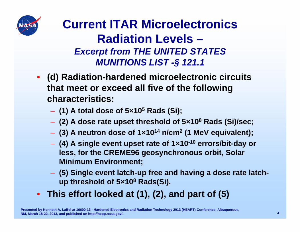
Current ITAR Microelectronics Radiation Levels –ad at o e e s
Excerpt from THE UNITED STATESMUNITIONS LIST -§ 121.1
• (d) Radiation-hardened microelectronic circuits that meet or exceed all five of the following characteristics:characteristics:– (1) A total dose of 5×10⁵ Rads (Si);– (2) A dose rate upset threshold of 5×10⁸ Rads (Si)/sec;
(3) A t d f 1×10¹⁴ / 2 (1 M V i l t)– (3) A neutron dose of 1×10¹⁴ n/cm2 (1 MeV equivalent); – (4) A single event upset rate of 1×10⁻¹⁰ errors/bit-day or
less, for the CREME96 geosynchronous orbit, Solar Mi i E i tMinimum Environment;
– (5) Single event latch-up free and having a dose rate latch-up threshold of 5×10⁸ Rads(Si).
Presented by Kenneth A. LaBel at 16600-13 - Hardened Electronics and Radiation Technology 2013 (HEART) Conference, Albuquerque, NM, March 18-22, 2013, and published on http://nepp.nasa.gov/.
• This effort looked at (1), (2), and part of (5)
4
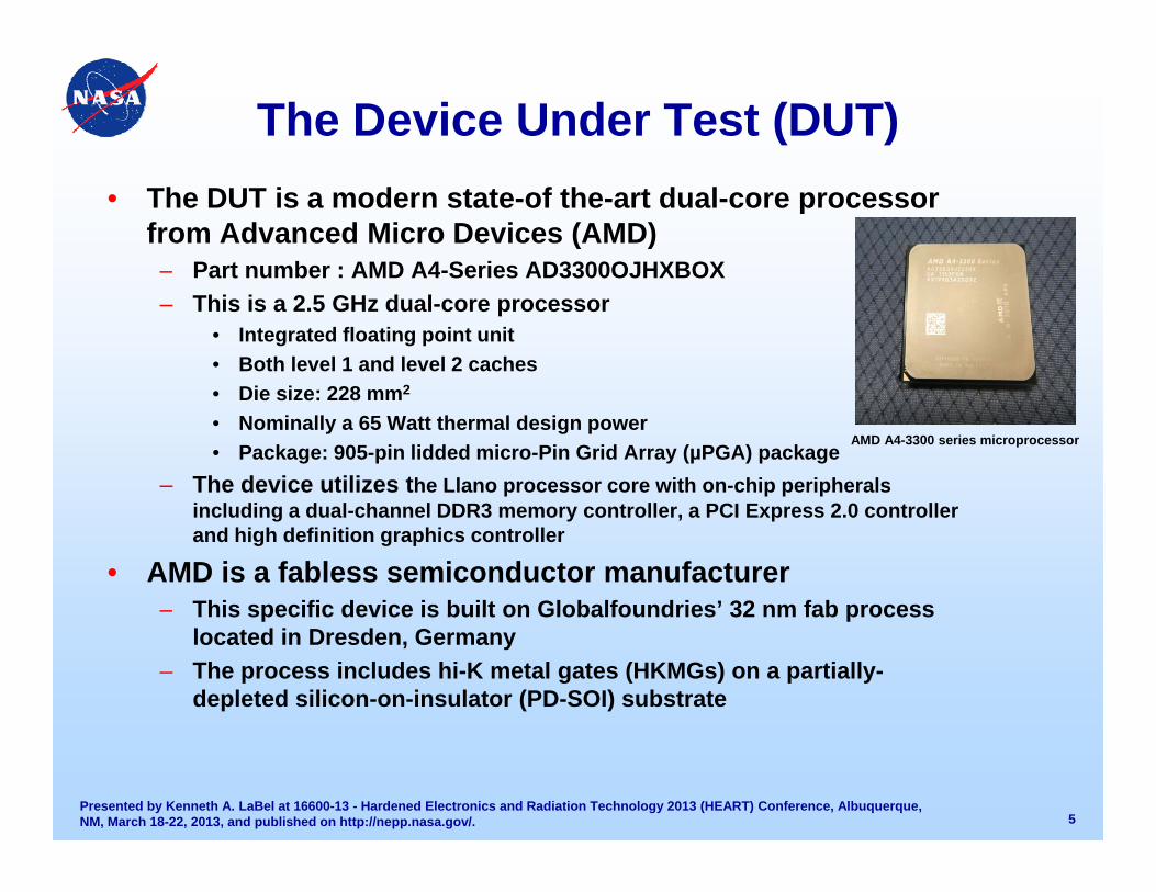
The Device Under Test (DUT)• The DUT is a modern state-of the-art dual-core processor
from Advanced Micro Devices (AMD)– Part number : AMD A4-Series AD3300OJHXBOXPart number : AMD A4 Series AD3300OJHXBOX – This is a 2.5 GHz dual-core processor
• Integrated floating point unit• Both level 1 and level 2 caches
Die size: 228 mm2• Die size: 228 mm2
• Nominally a 65 Watt thermal design power• Package: 905-pin lidded micro-Pin Grid Array (µPGA) package
– The device utilizes the Llano processor core with on-chip peripherals
AMD A4-3300 series microprocessor
including a dual-channel DDR3 memory controller, a PCI Express 2.0 controller and high definition graphics controller
• AMD is a fabless semiconductor manufacturer– This specific device is built on Globalfoundries’ 32 nm fab processThis specific device is built on Globalfoundries 32 nm fab process
located in Dresden, Germany– The process includes hi-K metal gates (HKMGs) on a partially-
depleted silicon-on-insulator (PD-SOI) substrate
Presented by Kenneth A. LaBel at 16600-13 - Hardened Electronics and Radiation Technology 2013 (HEART) Conference, Albuquerque, NM, March 18-22, 2013, and published on http://nepp.nasa.gov/. 5
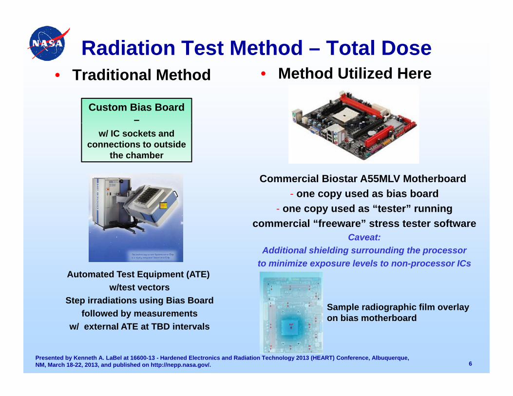
Radiation Test Method – Total Dose• Traditional Method • Method Utilized Here• Traditional Method • Method Utilized Here
Custom Bias Board –
w/ IC sockets and connections to outside
the chamber
Commercial Biostar A55MLV Motherboard - one copy used as bias board
- one copy used as “tester” runningcommercial “freeware” stress tester software
Automated Test Equipment (ATE)
commercial freeware stress tester softwareCaveat:
Additional shielding surrounding the processorto minimize exposure levels to non-processor ICs
Automated Test Equipment (ATE) w/test vectors
Step irradiations using Bias Boardfollowed by measurements
/
Sample radiographic film overlay on bias motherboard
Presented by Kenneth A. LaBel at 16600-13 - Hardened Electronics and Radiation Technology 2013 (HEART) Conference, Albuquerque, NM, March 18-22, 2013, and published on http://nepp.nasa.gov/. 6
w/ external ATE at TBD intervals
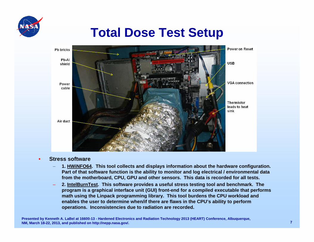
Total Dose Test Setup
• Stress software– 1 HWiNFO64 This tool collects and displays information about the hardware configuration1. HWiNFO64. This tool collects and displays information about the hardware configuration.
Part of that software function is the ability to monitor and log electrical / environmental data from the motherboard, CPU, GPU and other sensors. This data is recorded for all tests.
– 2. IntelBurnTest. This software provides a useful stress testing tool and benchmark. The program is a graphical interface unit (GUI) front-end for a compiled executable that performs math using the Linpack programming library. This tool burdens the CPU workload and
Presented by Kenneth A. LaBel at 16600-13 - Hardened Electronics and Radiation Technology 2013 (HEART) Conference, Albuquerque, NM, March 18-22, 2013, and published on http://nepp.nasa.gov/.
math using the Linpack programming library. This tool burdens the CPU workload and enables the user to determine when/if there are flaws in the CPU’s ability to perform operations. Inconsistencies due to radiation are recorded.
7
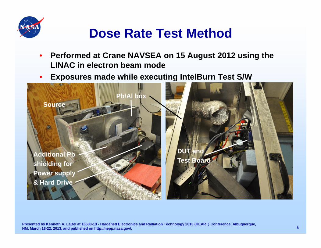
Dose Rate Test Method• Performed at Crane NAVSEA on 15 August 2012 using the
LINAC in electron beam mode• Exposures made while executing IntelBurn Test S/W• Exposures made while executing IntelBurn Test S/W
Pb/Al boxSource
Additional Pbshielding forP l
DUT and Test Board
Power supply & Hard Drive
Presented by Kenneth A. LaBel at 16600-13 - Hardened Electronics and Radiation Technology 2013 (HEART) Conference, Albuquerque, NM, March 18-22, 2013, and published on http://nepp.nasa.gov/. 8
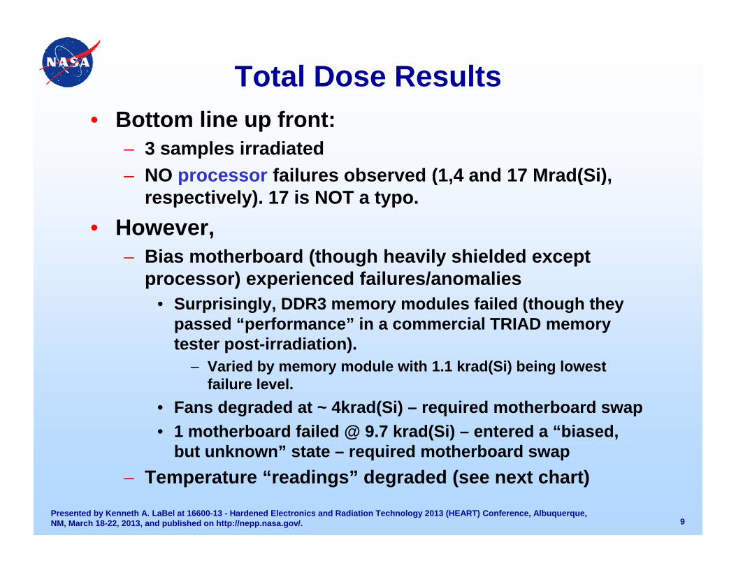
Total Dose Results• Bottom line up front:
– 3 samples irradiated– NO processor failures observed (1 4 and 17 Mrad(Si)– NO processor failures observed (1,4 and 17 Mrad(Si),
respectively). 17 is NOT a typo.• However,
– Bias motherboard (though heavily shielded except processor) experienced failures/anomalies
• Surprisingly, DDR3 memory modules failed (though they d “ f ” i i l TRIADpassed “performance” in a commercial TRIAD memory
tester post-irradiation).– Varied by memory module with 1.1 krad(Si) being lowest
failure level.• Fans degraded at ~ 4krad(Si) – required motherboard swap• 1 motherboard failed @ 9.7 krad(Si) – entered a “biased,
but unknown” state – required motherboard swap
Presented by Kenneth A. LaBel at 16600-13 - Hardened Electronics and Radiation Technology 2013 (HEART) Conference, Albuquerque, NM, March 18-22, 2013, and published on http://nepp.nasa.gov/.
– Temperature “readings” degraded (see next chart)
9
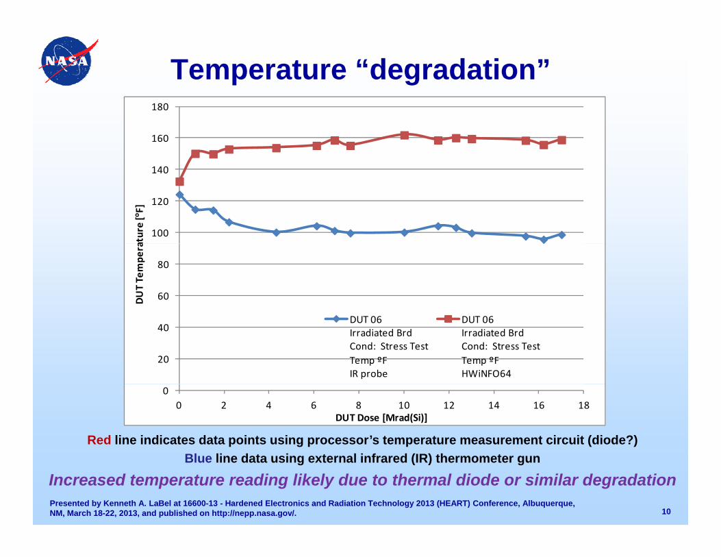
Temperature “degradation”
140
160
180
100
120
140
ature [ºF
]
60
80
DUT Tempe
ra
20
40DUT 06Irradiated BrdCond: Stress TestTemp ºFIR probe
DUT 06Irradiated BrdCond: Stress TestTemp ºFHWiNFO64
Red line indicates data points using processor’s temperature measurement circuit (diode?)Bl li d t i t l i f d (IR) th t
00 2 4 6 8 10 12 14 16 18
DUT Dose [Mrad(Si)]
Presented by Kenneth A. LaBel at 16600-13 - Hardened Electronics and Radiation Technology 2013 (HEART) Conference, Albuquerque, NM, March 18-22, 2013, and published on http://nepp.nasa.gov/. 10
Blue line data using external infrared (IR) thermometer gun
Increased temperature reading likely due to thermal diode or similar degradation
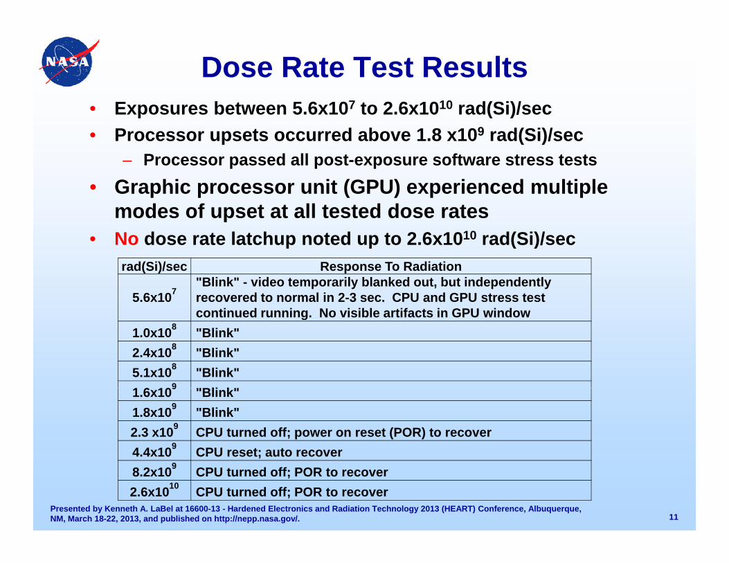
Dose Rate Test ResultsE b t 5 6 107 t 2 6 1010 d(Si)/• Exposures between 5.6x10⁷ to 2.6x10¹⁰ rad(Si)/sec
• Processor upsets occurred above 1.8 x10⁹ rad(Si)/sec– Processor passed all post-exposure software stress tests
• Graphic processor unit (GPU) experienced multiple modes of upset at all tested dose rates
• No dose rate latchup noted up to 2.6x10¹⁰ rad(Si)/secp p ( )rad(Si)/sec Response To Radiation
5.6x10⁷"Blink" - video temporarily blanked out, but independently recovered to normal in 2-3 sec. CPU and GPU stress test continued running. No visible artifacts in GPU windowcontinued running. No visible artifacts in GPU window
1.0x10⁸ "Blink"2.4x10⁸ "Blink"5.1x10⁸ "Blink"1 6 109 "Bli k"1.6x10⁹ "Blink"1.8x10⁹ "Blink"2.3 x10⁹ CPU turned off; power on reset (POR) to recover4.4x109 CPU reset; auto recover
Presented by Kenneth A. LaBel at 16600-13 - Hardened Electronics and Radiation Technology 2013 (HEART) Conference, Albuquerque, NM, March 18-22, 2013, and published on http://nepp.nasa.gov/. 11
8.2x10⁹ CPU turned off; POR to recover2.6x1010 CPU turned off; POR to recover
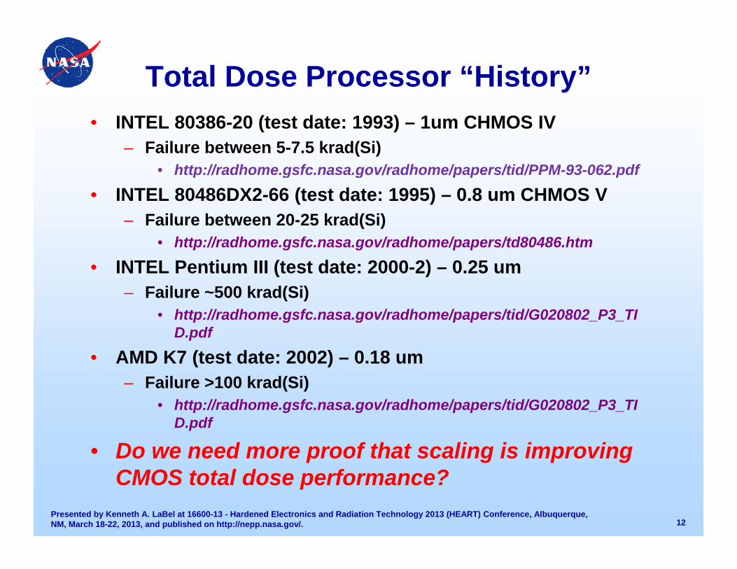
Total Dose Processor “History”• INTEL 80386-20 (test date: 1993) – 1um CHMOS IV
– Failure between 5-7.5 krad(Si)• http://radhome.gsfc.nasa.gov/radhome/papers/tid/PPM-93-062.pdfp g g p p p
• INTEL 80486DX2-66 (test date: 1995) – 0.8 um CHMOS V– Failure between 20-25 krad(Si)
• http://radhome.gsfc.nasa.gov/radhome/papers/td80486.htmp g g p p• INTEL Pentium III (test date: 2000-2) – 0.25 um
– Failure ~500 krad(Si)• http://radhome.gsfc.nasa.gov/radhome/papers/tid/G020802 P3 TIp g g p p _ _
D.pdf• AMD K7 (test date: 2002) – 0.18 um
– Failure >100 krad(Si)• http://radhome.gsfc.nasa.gov/radhome/papers/tid/G020802_P3_TI
D.pdf
• Do we need more proof that scaling is improving
Presented by Kenneth A. LaBel at 16600-13 - Hardened Electronics and Radiation Technology 2013 (HEART) Conference, Albuquerque, NM, March 18-22, 2013, and published on http://nepp.nasa.gov/.
CMOS total dose performance?
12
Takeaway Thoughts
• Digital CMOS devices– Definitely can exceed ITAR criteria tested here withoutDefinitely can exceed ITAR criteria tested here without
any intentional hardening• However, multiple support/peripheral devices
(i di th ) f il d t l l(i.e., surrounding the processor) failed at levels well below ITAR criteria– Likely bipolar or analog functions
• No ONE conclusion can be made whether “commercial technology is pushing the ITAR envelope inadvertently”envelope inadvertently– Depends on the technology and device, BUT the
potential for some devices to “push” is there
Presented by Kenneth A. LaBel at 16600-13 - Hardened Electronics and Radiation Technology 2013 (HEART) Conference, Albuquerque, NM, March 18-22, 2013, and published on http://nepp.nasa.gov/. 13
Summary and Acknowledgements• We presented a representative set of total dose
and dose rate data on a 32um SOI processor– Data shows this technology can pass certain ITARData shows this technology can pass certain ITAR
criteria– Data shows that support/peripheral devices may fail
certain ITAR criteriacertain ITAR criteria• A new hardness assurance method was
presented using commercial motherboards as “bi ” d t t b d ibl t i t“bias” and test boards – possible extension to future system on a chip (SOC) testing.
• AcknowledgementsAcknowledgements– NASA Electronic Parts and Packaging Program– NAVSEA Crane
D f Th t R d ti A
Presented by Kenneth A. LaBel at 16600-13 - Hardened Electronics and Radiation Technology 2013 (HEART) Conference, Albuquerque, NM, March 18-22, 2013, and published on http://nepp.nasa.gov/.
– Defense Threat Reduction Agency– National Reconnaissance Office
14