tle2426 high precision virtual ground
DESCRIPTION
check out our awesome datasheets! Lol screw scribdTRANSCRIPT

SLOS098D − AUGUST 1991 − REVISED MAY 1998
1POST OFFICE BOX 655303 • DALLAS, TEXAS 75265
1/2 VI Virtual Ground for Analog Systems
Self-Contained 3-terminal TO-226AAPackage
Micropower Operation . . . 170 µA Typ, VI = 5 V
Wide VI Range . . . 4 V to 40 V
High Output-Current Capability− Source . . . 20 mA Typ− Sink . . . 20 mA Typ
Excellent Output Regulation− −45 µV Typ at I O = 0 to −10 mA− +15 µV Typ at I O = 0 to +10 mA
Low-Impedance Output . . . 0.0075 Ω Typ
Noise Reduction Pin (D, JG, and PPackages Only)
description
In signal-conditioning applications utilizing asingle power source, a reference voltage equal toone-half the supply voltage is required fortermination of all analog signal grounds. TexasInstruments presents a precision virtual groundwhose output voltage is always equal to one-halfthe input voltage, the TLE2426 “rail splitter.”
The unique combination of a high-performance,micropower operational amplifier and a precision-trimmed divider on a single silicon chip results ina precise VO/VI ratio of 0.5 while sinking andsourcing current. The TLE2426 provides a low-impedance output with 20 mA of sink and sourcecapability while drawing less than 280 µAof supply current over the full input range of 4 V to 40 V. A designer need not pay the price in terms of boardspace for a conventional signal ground consisting of resistors, capacitors, operational amplifiers, and voltagereferences. The performance and precision of the TLE2426 is available in an easy-to-use, space saving,3-terminal LP package. For increased performance, the optional 8-pin packages provide a noise-reduction pin.With the addition of an external capacitor (CNR), peak-to-peak noise is reduced while line ripple rejection isimproved.
Initial output tolerance for a single 5-V or 12-V system is better than 1% with 3.6% over the full 40-V input range.Ripple rejection exceeds 12 bits of accuracy. Whether the application is for a data acquisition front end, analogsignal termination, or simply a precision voltage reference, the TLE2426 eliminates a major source of systemerror.
AVAILABLE OPTIONS
PACKAGED DEVICESCHIP
TASMALL
OUTLINE(D)
CERAMICDIP(JG)
PLASTIC (LP)
PLASTICDIP(P)
CHIPFORM
(Y)
0°C to 70°C TLE2426CD — TLE2426CLP TLE2426CP
Please be aware that an important notice concerning availability, standard warranty, and use in critical applications ofTexas Instruments semiconductor products and disclaimers thereto appears at the end of this data sheet.
! " #$%! " &$'(#! )!%*)$#!" # ! "&%##!" &% !+% !%" %," "!$%!""!)) -!.* )$#! &#%""/ )%" ! %#%""(. #($)%!%"!/ (( &%!%"*
Copyright 1998, Texas Instruments Incorporated
VO
VI
4
2
0
8
6
0 0.25 0.5 0.75 1
Vol
tage
− V
t − Time − s
INPUT/OUTPUT TRANSFER CHARACTERISTICS
10
VO
VI2
VI VO

SLOS098D − AUGUST 1991 − REVISED MAY 1998
2 POST OFFICE BOX 655303 • DALLAS, TEXAS 75265
−40°C to 85°C TLE2426ID — TLE2426ILP TLE2426IP TLE2426Y
−55°C to 125°C TLE2426MD TLE2426MJG TLE2426MLP TLE2426MP
The D and LP packages are available taped and reeled in the commercial temperature range only. Add R suffixto the device type (e. g., TLC2426CDR). Chips are tested at 25°C.

SLOS098D − AUGUST 1991 − REVISED MAY 1998
3POST OFFICE BOX 655303 • DALLAS, TEXAS 75265
description (continued)
The C-suffix devices are characterized for operation from 0°C to 70°C. The I suffix devices are characterizedfor operation from −40°C to 85°C. The M suffix devices are characterized over the full military temperature rangeof −55°C to 125°C.
OUT
IN
COMMON
1
2
3
4
8
7
6
5
OUTCOMMON
INNC
NOISE REDUCTIONNCNCNC
D, JG, OR P PACKAGE(TOP VIEW)
NC − No internal connection
LP PACKAGE(TOP VIEW)
TLE2426Y chip information
This chip, properly assembled, displays characteristics similar to the TLE2426C. Thermal compression orultrasonic bonding may be used on the doped aluminum bonding pads. The chips may be mounted withconductive epoxy or a gold-silicon preform.
BONDING PAD ASSIGNMENTS
CHIP THICKNESS:15 MILS TYPICAL
BONDING PADS:4 × 4 MILS MINIMUM
TJmax = 150°C
TOLERANCES ARE ±10%.
ALL DIMENSIONS ARE INMILS.
60
88
OUT(1)
(2)
(8)
(3)
NOISEREDUCTION
IN
COMMON
+1
NOTE A: Both bonding pads numbered 1, both numbered 2,and both numbered 3, must be bonded out to thecorresponding functions pin.
(3) (3)(2) (2)
(1) (1)
(8)

SLOS098D − AUGUST 1991 − REVISED MAY 1998
4 POST OFFICE BOX 655303 • DALLAS, TEXAS 75265
absolute maximum ratings over operating free-air temperature (unless otherwise noted) †
Continuous input voltage, VI 40 V. . . . . . . . . . . . . . . . . . . . . . . . . . . . . . . . . . . . . . . . . . . . . . . . . . . . . . . . . . . . . . . . . Continuous filter trap voltage 40 V. . . . . . . . . . . . . . . . . . . . . . . . . . . . . . . . . . . . . . . . . . . . . . . . . . . . . . . . . . . . . . . . Output current, IO ±80 mA. . . . . . . . . . . . . . . . . . . . . . . . . . . . . . . . . . . . . . . . . . . . . . . . . . . . . . . . . . . . . . . . . . . . . . . Duration of short-circuit current at (or below) 25°C (see Note 1) unlimited. . . . . . . . . . . . . . . . . . . . . . . . . . . . . . Continuous total power dissipation See Dissipation Rating Table. . . . . . . . . . . . . . . . . . . . . . . . . . . . . . . . . . . . . Operating free-air temperature range, TA: C suffix 0°C to 70°C. . . . . . . . . . . . . . . . . . . . . . . . . . . . . . . . . . . . . .
I suffix −40°C to 85°C. . . . . . . . . . . . . . . . . . . . . . . . . . . . . . . . . . . . . M suffix −55°C to 125°C. . . . . . . . . . . . . . . . . . . . . . . . . . . . . . . . . .
Storage temperature range, Tstg −65°C to 150°C. . . . . . . . . . . . . . . . . . . . . . . . . . . . . . . . . . . . . . . . . . . . . . . . . . . Lead temperature 1,6 mm (1/16 inch) from case for 10 seconds: D or P package 260°C. . . . . . . . . . . . . . . . . Lead temperature 1,6 mm (1/16 inch) from case for 60 seconds: JG or LP package 300°C. . . . . . . . . . . . . .
† Stresses beyond those listed under “absolute maximum ratings” may cause permanent damage to the device. These are stress ratings only, andfunctional operation of the device at these or any other conditions beyond those indicated under “recommended operating conditions” is notimplied. Exposure to absolute-maximum-rated conditions for extended periods may affect device reliability.
NOTE 1: The output may be shorted to either supply. Temperature and/or supply voltages must be limited to ensure that the maximum dissipationrating is not exceeded.
DISSIPATION RATING TABLE
PACKAGETA ≤ 25°C DERATING FACTOR TA = 70°C TA = 85°C TA = 125°C
PACKAGETA ≤ 25 C
POWER RATINGDERATING FACTORABOVE TA = 25°C
TA = 70 CPOWER RATING
TA = 85 CPOWER RATING
TA = 125 CPOWER RATING
D 725 mV 5.8 mW/°C 464 mW 377 mW 145 mW
JG 1050 mV 8.4 mW/°C 672 mW 546 mW 210 mW
LP 775 mV 6.2 mW/°C 496 mW 403 mW 155 mW
P 1000 mV 8.0 mW/°C 640 mW 520 mW 200 mW
recommended operating conditions
C SUFFIX I SUFFIX M SUFFIXUNIT
MIN MAX MIN MAX MIN MAXUNIT
Input voltage, VI 4 40 4 40 4 40 V
Operating free-air temperature, TA 0 70 −40 85 −55 125 °C

SLOS098D − AUGUST 1991 − REVISED MAY 1998
5POST OFFICE BOX 655303 • DALLAS, TEXAS 75265
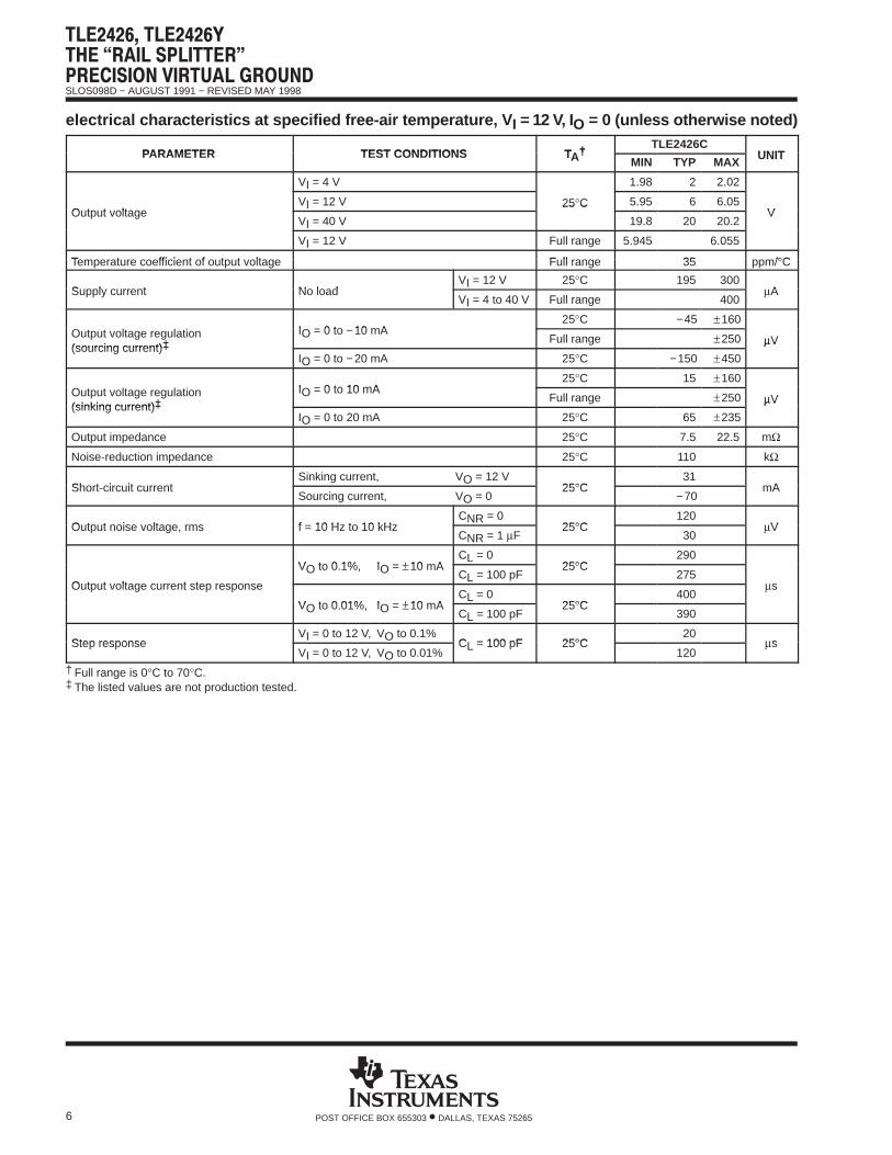
electrical characteristics at specified free-air temperature, V I = 5 V, IO = 0 (unless otherwise noted)
PARAMETER TEST CONDITIONS TA†TLE2426C
UNITPARAMETER TEST CONDITIONS TA†MIN TYP MAX
UNIT
VI = 4 V 1.98 2 2.02
Output voltageVI = 5 V 25°C 2.48 2.5 2.52
VOutput voltageVI = 40 V
25 C
19.8 20 20.2V
VI = 5 V Full range 2.475 2.525
Temperature coefficient of output voltage Full range 25 ppm/°CTemperature coefficient of output voltage Full range 25 ppm/°C
Supply current No loadVI = 5 V 25°C 170 300
ASupply current No loadVI = 4 to 40 V Full range 400
µA
Output voltage regulation IO = 0 to −10 mA25°C −45 ±160
Output voltage regulation (sourcing current)‡
IO = 0 to −10 mAFull range ±250 µV
(sourcing current)‡IO = 0 to −20 mA 25°C −150 ±450
µV
Output voltage regulation IO = 0 to 10 mA25°C 15 ±160
Output voltage regulation (sinking current)‡
IO = 0 to 10 mAFull range ±250 µV
(sinking current)‡IO = 0 to 20 mA 25°C 65 ±235
µV
Output impedance 25°C 7.5 22.5 mΩ
Noise-reduction impedance 25°C 110 kΩ
Short-circuit currentSinking current, VO = 5 V
25°C26
mAShort-circuit currentSourcing current, VO = 0
25°C−47
mA
Output noise voltage, rms f = 10 Hz to 10 kHzCNR = 0
25°C120
VOutput noise voltage, rms f = 10 Hz to 10 kHzCNR = 1 µF
25°C30
µV
VO to 0.1%, IO = ±10 mACL = 0
25°C290
Output voltage current step response
VO to 0.1%, IO = ±10 mACL = 100 pF
25°C275
sOutput voltage current step response
VO to 0.01%, IO = ±10 mACL = 0
25°C400
µs
VO to 0.01%, IO = ±10 mACL = 100 pF
25°C390
Step responseVI = 0 to 5 V, VO to 0.1%
CL = 100 pF 25°C20
µsStep responseVI = 0 to 5 V, VO to 0.01%
CL = 100 pF 25°C160
µs
† Full range is 0°C to 70°C.‡ The listed values are not production tested.
SLOS098D − AUGUST 1991 − REVISED MAY 1998
6 POST OFFICE BOX 655303 • DALLAS, TEXAS 75265
electrical characteristics at specified free-air temperature, V I = 12 V, IO = 0 (unless otherwise noted)
PARAMETER TEST CONDITIONS TA†TLE2426C
UNITPARAMETER TEST CONDITIONS TA†MIN TYP MAX
UNIT
VI = 4 V 1.98 2 2.02
Output voltageVI = 12 V 25°C 5.95 6 6.05
VOutput voltageVI = 40 V
25 C
19.8 20 20.2V
VI = 12 V Full range 5.945 6.055
Temperature coefficient of output voltage Full range 35 ppm/°CTemperature coefficient of output voltage Full range 35 ppm/°C
Supply current No loadVI = 12 V 25°C 195 300
ASupply current No loadVI = 4 to 40 V Full range 400
µA
Output voltage regulation IO = 0 to −10 mA25°C −45 ±160
Output voltage regulation (sourcing current)‡
IO = 0 to −10 mAFull range ±250 µV
(sourcing current)‡IO = 0 to −20 mA 25°C −150 ±450
µV
Output voltage regulation IO = 0 to 10 mA25°C 15 ±160
Output voltage regulation (sinking current)‡
IO = 0 to 10 mAFull range ±250 µV
(sinking current)‡IO = 0 to 20 mA 25°C 65 ±235
µV
Output impedance 25°C 7.5 22.5 mΩ
Noise-reduction impedance 25°C 110 kΩ
Short-circuit currentSinking current, VO = 12 V
25°C31
mAShort-circuit currentSourcing current, VO = 0
25°C−70
mA
Output noise voltage, rms f = 10 Hz to 10 kHzCNR = 0
25°C120
VOutput noise voltage, rms f = 10 Hz to 10 kHzCNR = 1 µF
25°C30
µV
VO to 0.1%, IO = ±10 mACL = 0
25°C290
Output voltage current step response
VO to 0.1%, IO = ±10 mACL = 100 pF
25°C275
sOutput voltage current step response
VO to 0.01%, IO = ±10 mACL = 0
25°C400
µs
VO to 0.01%, IO = ±10 mACL = 100 pF
25°C390
Step responseVI = 0 to 12 V, VO to 0.1%
CL = 100 pF 25°C20
µsStep responseVI = 0 to 12 V, VO to 0.01%
CL = 100 pF 25°C120
µs
† Full range is 0°C to 70°C.‡ The listed values are not production tested.

SLOS098D − AUGUST 1991 − REVISED MAY 1998
7POST OFFICE BOX 655303 • DALLAS, TEXAS 75265
electrical characteristics at specified free-air temperature, V I = 5 V, IO = 0 (unless otherwise noted)
PARAMETER TEST CONDITIONS TA†TLE2426I
UNITPARAMETER TEST CONDITIONS TA†MIN TYP MAX
UNIT
VI = 4 V 1.98 2 2.02
Output voltageVI = 5 V 25°C 2.48 2.5 2.52
VOutput voltageVI = 40 V
25 C
19.8 20 20.2V
VI = 5 V Full range 2.47 2.53
Temperature coefficient of output volt-Full range 25 ppm/°C
Temperature coefficient of output volt-age Full range 25 ppm/°C
Supply current No loadVI = 5 V 25°C 170 300
ASupply current No loadVI = 4 to 40 V Full range 400
µA
Output voltage regulation IO = 0 to −10 mA25°C −45 ±160
Output voltage regulation (sourcing current)‡
IO = 0 to −10 mAFull range ±250 µV
(sourcing current)‡IO = 0 to −20 mA 25°C −150 ±450
µV
Output voltage regulation IO = 0 to 10 mA 25°C 15 ±160
Output voltage regulation (sinking current)‡
IO = 0 to 8 mA Full range ±250 µV(sinking current)‡
IO = 0 to 20 mA 25°C 65 ±235
µV
Output impedance 25°C 7.5 22.5 mΩ
Noise-reduction impedance 25°C 110 kΩ
Short-circuit currentSinking current, VO = 5 V
25°C26
mAShort-circuit currentSourcing current, VO = 0
25°C−47
mA
Output noise voltage, rms f = 10 Hz to 10 kHzCNR = 0
25°C120
VOutput noise voltage, rms f = 10 Hz to 10 kHzCNR = 1 µF
25°C30
µV
VO to 0.1%, IO = ±10 mACL = 0
25°C290
Output voltage current step response
VO to 0.1%, IO = ±10 mACL = 100 pF
25°C275
sOutput voltage current step response
VO to 0.01%, IO = ±10 mACL = 0
25°C400
µs
VO to 0.01%, IO = ±10 mACL = 100 pF
25°C390
Step responseVI = 0 to 5 V, VO to 0.1%
CL = 100 pF 25°C20
µsStep responseVI = 0 to 5 V, VO to 0.01%
CL = 100 pF 25°C160
µs
† Full range is −40°C to 85°C.‡ The listed values are not production tested.

SLOS098D − AUGUST 1991 − REVISED MAY 1998
8 POST OFFICE BOX 655303 • DALLAS, TEXAS 75265
electrical characteristics at specified free-air temperature, V I = 12 V, IO = 0 (unless otherwise noted)
PARAMETER TEST CONDITIONS TA†TLE2426I
UNITPARAMETER TEST CONDITIONS TA†MIN TYP MAX
UNIT
VI = 4 V 1.98 2 2.02
Output voltageVI = 12 V 25°C 5.95 6 6.05
VOutput voltageVI = 40 V
25 C
19.8 20 20.2V
VI = 12 V Full range 5.935 6.065
Temperature coefficient of output voltage Full range 35 ppm/°CTemperature coefficient of output voltage Full range 35 ppm/°C
Supply current No loadVI = 12 V 25°C 195 300
ASupply current No loadVI = 4 to 40 V Full range 400
µA
Output voltage regulation IO = 0 to −10 mA25°C −45 ±160
Output voltage regulation (sourcing current)‡
IO = 0 to −10 mAFull range ±250 µV
(sourcing current)‡IO = 0 to −20 mA 25°C −150 ±450
µV
Output voltage regulation IO = 0 to 10 mA 25°C 15 ±160
Output voltage regulation (sinking current)‡
IO = 0 to 8 mA Full range ±250 µV(sinking current)‡
IO = 0 to 20 mA 25°C 65 ±235
µV
Output impedance 25°C 7.5 22.5 mΩ
Noise-reduction impedance 25°C 110 kΩ
Short-circuit currentSinking current, VO = 12 V
25°C31
mAShort-circuit currentSourcing current, VO = 0
25°C−70
mA
Output noise voltage, rms f = 10 Hz to 10 kHzCNR = 0
25°C120
VOutput noise voltage, rms f = 10 Hz to 10 kHzCNR = 1 µF
25°C30
µV
VO to 0.1%, IO = ±10 mACL = 0
25°C290
Output voltage current step response
VO to 0.1%, IO = ±10 mACL = 100 pF
25°C275
sOutput voltage current step response
VO to 0.01%, IO = ±10 mACL = 0
25°C400
µs
VO to 0.01%, IO = ±10 mACL = 100 pF
25°C390
Step responseVI = 0 to 12 V, VO to 0.1%
CL = 100 pF 25°C20
µsStep responseVI = 0 to 12 V, VO to 0.01%
CL = 100 pF 25°C120
µs
† Full range is −40°C to 85°C.‡ The listed values are not production tested.

SLOS098D − AUGUST 1991 − REVISED MAY 1998
9POST OFFICE BOX 655303 • DALLAS, TEXAS 75265
electrical characteristics at specified free-air temperature, V I = 5 V, IO = 0 (unless otherwise noted)
PARAMETER TEST CONDITIONS TA†TLE2426M
UNITPARAMETER TEST CONDITIONS TA†MIN TYP MAX
UNIT
VI = 4 V 1.98 2 2.02
Output voltageVI = 5 V 25°C 2.48 2.5 2.52
VOutput voltageVI = 40 V
25 C
19.8 20 20.2V
VI = 5 V Full range 2.465 2.535
Temperature coefficient of output voltage Full range 25 ppm/°CTemperature coefficient of output voltage Full range 25 ppm/°C
Supply current No loadVI = 5 V 25°C 170 300
ASupply current No loadVI = 4 to 40 V Full range 400
µA
Output voltage regulation IO = 0 to −10 mA25°C −45 ±160
Output voltage regulation (sourcing current)‡
IO = 0 to −10 mAFull range ±250 µV
(sourcing current)‡IO = 0 to −20 mA 25°C −150 ±450
µV
Output voltage regulation IO = 0 to 10 mA 25°C 15 ±160
Output voltage regulation (sinking current)‡
IO = 0 to 3 mA Full range ±250 µV(sinking current)‡
IO = 0 to 20 mA 25°C 65 ±235
µV
Output impedance 25°C 7.5 22.5 mΩ
Noise-reduction impedance 25°C 110 kΩ
Short-circuit currentSinking current, VO = 5 V
25°C26
mAShort-circuit currentSourcing current, VO = 0
25°C−47
mA
Output noise voltage, rms f = 10 Hz to 10 kHzCNR = 0
25°C120
VOutput noise voltage, rms f = 10 Hz to 10 kHzCNR = 1 µF
25°C30
µV
VO to 0.1%, IO = ±10 mACL = 0
25°C290
Output voltage current step response
VO to 0.1%, IO = ±10 mACL = 100 pF
25°C275
sOutput voltage current step response
VO to 0.01%, IO = ±10 mACL = 0
25°C400
µs
VO to 0.01%, IO = ±10 mACL = 100 pF
25°C390
Step responseVI = 0 to 5 V, VO to 0.1%
CL = 100 pF 25°C20
µsStep responseVI = 0 to 5 V, VO to 0.01%
CL = 100 pF 25°C120
µs
† Full range is −55°C to 125°C.‡ The listed values are not production tested.

SLOS098D − AUGUST 1991 − REVISED MAY 1998
10 POST OFFICE BOX 655303 • DALLAS, TEXAS 75265
electrical characteristics at specified free-air temperature, V I = 12 V, IO = 0 (unless otherwise noted)
PARAMETER TEST CONDITIONS TA†TLE2426M
UNITPARAMETER TEST CONDITIONS TA†MIN TYP MAX
UNIT
VI = 4 V 1.98 2 2.02
Output voltageVI = 12 V 25°C 5.95 6 6.05
VOutput voltageVI = 40 V
25 C
19.8 20 20.2V
VI = 12 V Full range 5.925 6.075
Temperature coefficient of output voltage Full range 35 ppm/°CTemperature coefficient of output voltage Full range 35 ppm/°C
Supply current No loadVI = 12 V 25°C 195 250
ASupply current No loadVI = 4 to 40 V Full range 350
µA
Output voltage regulation IO = 0 to −10 mA25°C −45 ±160
Output voltage regulation (sourcing current)‡
IO = 0 to −10 mAFull range ±250 µV
(sourcing current)‡IO = 0 to −20 mA 25°C −150 ±450
µV
Output voltage regulation IO = 0 to 10 mA 25°C 15 ±160
Output voltage regulation (sinking current)‡
IO = 0 to 8 mA Full range ±250 µV(sinking current)‡
IO = 0 to 20 mA 25°C 65 ±235
µV
Output impedance 25°C 7.5 22.5 mΩ
Noise-reduction impedance 25°C 110 kΩ
Short-circuit currentSinking current, VO = 12 V
25°C31
mAShort-circuit currentSourcing current, VO = 0
25°C−70
mA
Output noise voltage, rms f = 10 Hz to 10 kHzCNR = 0
25°C120
VOutput noise voltage, rms f = 10 Hz to 10 kHzCNR = 1 µF
25°C30
µV
VO to 0.1%, IO = ±10 mACL = 0
25°C290
Output voltage current step response
VO to 0.1%, IO = ±10 mACL = 100 pF
25°C275
sOutput voltage current step response
VO to 0.01%, IO = ±10 mACL = 0
25°C400
µs
VO to 0.01%, IO = ±10 mACL = 100 pF
25°C390
Step responseVI = 0 to 12 V, VO to 0.1%
CL = 100 pF 25°C12
µsStep responseVI = 0 to 12 V, VO to 0.01%
CL = 100 pF 25°C120
µs
† Full range is −55°C to 125°C.‡ The listed values are not production tested.

SLOS098D − AUGUST 1991 − REVISED MAY 1998
11POST OFFICE BOX 655303 • DALLAS, TEXAS 75265
electrical characteristics at specified free-air temperature, V I = 5 V, IO = 0, TA = 25°C (unlessotherwise noted)
PARAMETER TEST CONDITIONSTLE2426Y
UNITPARAMETER TEST CONDITIONSMIN TYP MAX
UNIT
Output voltage VI = 5 V 2.5 V
Supply current No load 170 µA
Output voltage regulation (sourcing current)†IO = 0 to −10 mA −45
µVOutput voltage regulation (sourcing current)†IO = 0 to −20 mA −150
µV
Output voltage regulation (sinking current)†IO = 0 to 10 mA 15
µVOutput voltage regulation (sinking current)†IO = 0 to 20 mA 65
µV
Output impedance 7.5 mΩNoise-reduction impedance 110 kΩ
Short-circuit currentSinking current, VO = 5 V 26
mAShort-circuit currentSourcing current, VO = 0 −47
mA
Output noise voltage, rms f = 10 Hz to 10 kHzCNR = 0 120
µVOutput noise voltage, rms f = 10 Hz to 10 kHzCNR = 1 µF 30
µV
VO to 0.1%, IO = ±10 mACL = 0 290
Output voltage current step response
VO to 0.1%, IO = ±10 mACL = 100 pF 275
µsOutput voltage current step response
VO to 0.01%, IO = ±10 mACL = 0 400
µs
VO to 0.01%, IO = ±10 mACL = 100 pF 390
Step responseVI = 0 to 5 V, VO to 0.1%
CL = 100 pF20
sStep responseVI = 0 to 5 V, VO to 0.01%
CL = 100 pF160
µs
† The listed values are not production tested.
electrical characteristics at specified free-air temperature, V I = 12 V, IO = 0, TA = 25°C (unlessotherwise noted)
PARAMETER TEST CONDITIONSTLE2426Y
UNITPARAMETER TEST CONDITIONSMIN TYP MAX
UNIT
Output voltage VI = 12 V 6 V
Supply current No load 195 µA
Output voltage regulation (sourcing current)†IO = 0 to −10 mA −45
µVOutput voltage regulation (sourcing current)†IO = 0 to −20 mA −150
µV
Output voltage regulation (sinking current)†IO = 0 to 3 mA 15
µVOutput voltage regulation (sinking current)†IO = 0 to 20 mA 65
µV
Output impedance 7.5 mΩNoise-reduction impedance 110 kΩ
Short-circuit currentSinking current, VO = 12 V 31
mAShort-circuit currentSourcing current, VO = 0 −70
mA
Output noise voltage, rms f = 10 Hz to 10 kHZCNR = 0 120
µVOutput noise voltage, rms f = 10 Hz to 10 kHZCNR = 1 µF 30
µV
VO to 0.1%, IO = ±10 mACL = 0 290
Output voltage current, step response
VO to 0.1%, IO = ±10 mACL = 100 pF 275
µsOutput voltage current, step response
VO to 0.01%, IO = ±10 mACL = 0 400
µs
VO to 0.01%, IO = ±10 mACL = 100 pF 390
Step responseVI = 0 to 12 V, VO to 0.1%
CL = 100 pF12
sStep responseVI = 0 to 12 V, VO to 0.01%
CL = 100 pF120
µs
† The listed values are not production tested.
SLOS098D − AUGUST 1991 − REVISED MAY 1998
12 POST OFFICE BOX 655303 • DALLAS, TEXAS 75265
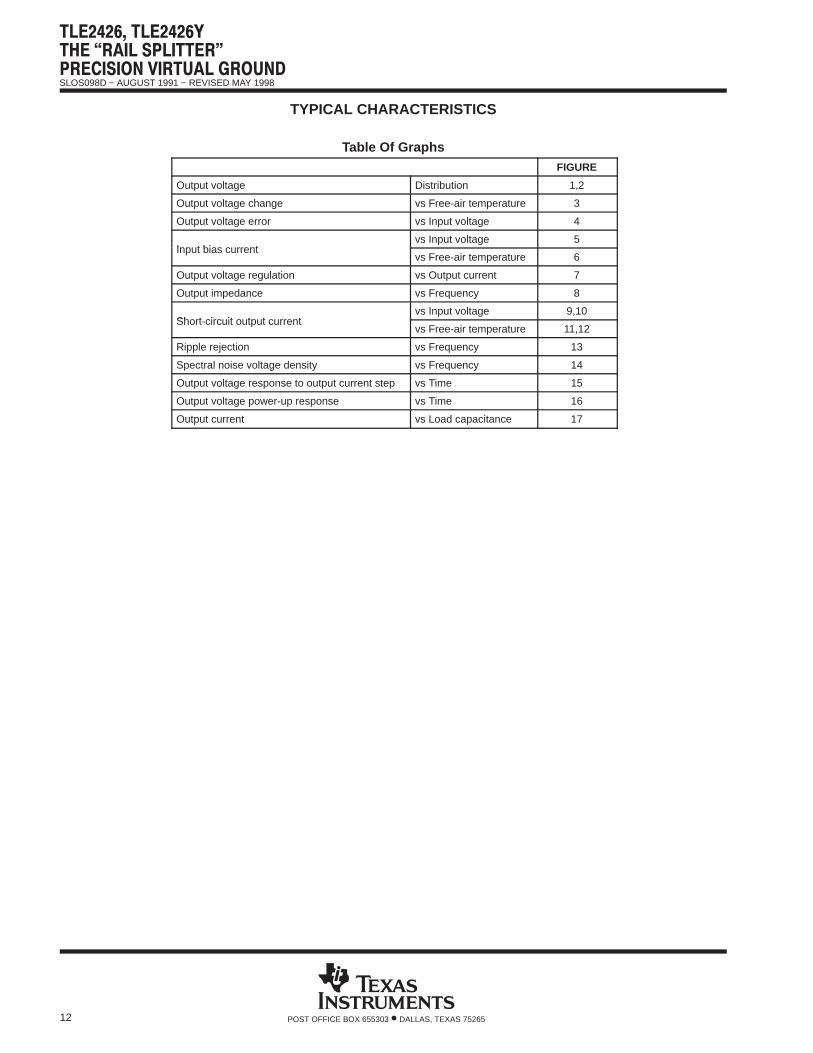
TYPICAL CHARACTERISTICS
Table Of GraphsFIGURE
Output voltage Distribution 1,2
Output voltage change vs Free-air temperature 3
Output voltage error vs Input voltage 4
Input bias currentvs Input voltage 5
Input bias currentvs Free-air temperature 6
Output voltage regulation vs Output current 7
Output impedance vs Frequency 8
Short-circuit output currentvs Input voltage 9,10
Short-circuit output currentvs Free-air temperature 11,12
Ripple rejection vs Frequency 13
Spectral noise voltage density vs Frequency 14
Output voltage response to output current step vs Time 15
Output voltage power-up response vs Time 16
Output current vs Load capacitance 17
SLOS098D − AUGUST 1991 − REVISED MAY 1998
13POST OFFICE BOX 655303 • DALLAS, TEXAS 75265
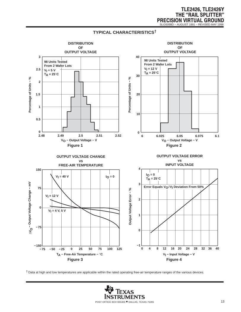
TYPICAL CHARACTERISTICS †
Figure 1
DISTRIBUTIONOF
OUTPUT VOLTAGE
2
1
0.5
0
3
1.5
2.48 2.49 2.5 2.51 2.52
Per
cent
age
of U
nits
− %
2.5
VO − Output Voltage − V
98 Units TestedFrom 2 Wafer LotsVI = 5 VTA = 25°C
Figure 2
6.05 6.075VO − Output Voltage − V
20
10
0
40
30
6 6.025 6.1
Per
cent
age
of U
nits
− %
DISTRIBUTIONOF
OUTPUT VOLTAGE
VI = 12 VTA = 25°C
98 Units TestedFrom 2 Wafer Lots
Figure 3
VO
− O
utpu
t Vol
tage
Cha
nge
− m
V
0
0 25 50
75
OUTPUT VOLTAGE CHANGEvs
FREE-AIR TEMPERATURE150
75 100 125
∆VO
TA − Free-Air Temperature − °C
VI = 40 V IO = 0
VI = 12 V
VI = 4 V, 5 V
−75
−150−75 −50 −25
Figure 4
2
1
0
−10 4 8 12 16 20
Out
put V
olta
ge E
rror
− %
3
OUTPUT VOLTAGE ERRORvs
INPUT VOLTAGE4
24 36 40
VI − Input Voltage − V
28 32
IO = 0TA = 25°C
Error Equals V O/VI Deviation From 50%
† Data at high and low temperatures are applicable within the rated operating free-air temperature ranges of the various devices.

SLOS098D − AUGUST 1991 − REVISED MAY 1998
14 POST OFFICE BOX 655303 • DALLAS, TEXAS 75265
TYPICAL CHARACTERISTICS †
Figure 5
150
100
50
00 5 10 15 20 25
200
250
INPUT BIAS CURRENTvs
INPUT VOLTAGE300
30 35 40
VI − Input Voltage − V
IO = 0
TA = −55°C
TA = 125°C
TA = 25°C
IIB −
Inpu
t Bia
s C
urre
nt −
I I
BA
µ
Figure 6
150
100
50
0
0 25 50
200
250
INPUT BIAS CURRENTvs
FREE-AIR TEMPERATURE300
75 100 125
VI = 40 V
VI = 12 V
VI = 5 V
VI = 4 V
IO = 0
TA − Free-Air Temperature − °C−50−75 −20
IIB −
Inpu
t Bia
s C
urre
nt −
I I
BA
µ
Figure 7
Min
IO − Output Current − mA
OUTPUT VOLTAGE REGULATIONvs
OUTPUT CURRENT
0
500
250
0 10 20
Max
Typ
Min
Max
Typ
VI = 5 V or 12 VTA = 25°C
−250
−500−20 −10
Out
put V
olta
ge R
egul
atio
n −
µV
Figure 8
1
0.1
0.01
0.001
10 100 1 k
10
f − Frequency − Hz
100
10 k 100 k 1 M
OUTPUT IMPEDANCEvs
FREQUENCY
VI = 5 V or 12 VIO = 0TA = 25°C
− O
utpu
t Im
peda
nce
− Ω
zo
† Data at high and low temperatures are applicable within the rated operating free-air temperature ranges of the various devices.

SLOS098D − AUGUST 1991 − REVISED MAY 1998
15POST OFFICE BOX 655303 • DALLAS, TEXAS 75265
TYPICAL CHARACTERISTICS †
Figure 9
0 5 10 15 20 25
SHORT-CIRCUIT OUTPUT CURRENTvs
INPUT VOLTAGE
0
30 35 40
IOS
− S
hort
-Circ
uit O
utpu
t Cur
rent
− m
AI O
S
VI − Input Voltage − V
VO = GND(Output Sourcing)
TA = 25°C
TA = −55°C
TA = 125°C
−20
−40
−60
−80
Figure 10VI − Input Voltage − V
20
10
00 5 10 15 20 25
30
SHORT-CIRCUIT OUTPUT CURRENTvs
INPUT VOLTAGE
40
30 35 40
IOS
− S
hort
-Circ
uit O
utpu
t Cur
rent
− m
AI O
S
VO = VI(Output Sinking)
TA = −55°C
TA = 125°C
TA = 25°C
Figure 11
125
0
IOS
− S
hort
-Circ
uit O
utpu
t Cur
rent
− m
AI O
S
TA − Free-Air Temperature − °C
SHORT-CIRCUIT OUTPUT CURRENTvs
FREE-AIR TEMPERATURE
0 25 50 75 100
VI = 12 V
VI = 4 VVO = GND
(Output Sourcing)−10
−20
−30
−40
−50
−60
−70
−80−75 −50 −25
VI = 5 V
VI = 40 V
Figure 12
SHORT-CIRCUIT OUTPUT CURRENTvs
FREE-AIR TEMPERATURE
20
10
00 25 50
30
40
75 100 125
IOS
− S
hort
-Circ
uit O
utpu
t Cur
rent
− m
AI O
S
TA − Free-Air Temperature − °C
VI = 4 V
VI = 5 V
VI = 12 V
VI = 40 V
VO = VI(Output Sinking)
−75 −50 −25
† Data at high and low temperatures are applicable within the rated operating free-air temperature ranges of the various devices.

SLOS098D − AUGUST 1991 − REVISED MAY 1998
16 POST OFFICE BOX 655303 • DALLAS, TEXAS 75265
TYPICAL CHARACTERISTICS
Figure 13
50
40
20
10
0
90
30
10 100 1 k 10 k
Rip
ple
Rej
ectio
n −
dB
70
60
80
RIPPLE REJECTIONvs
FREQUENCY
100
100 k 1 M
f − Frequency − Hz
VI = 5 V or 12 V∆VI(PP) = 1 VIO = 0TA = 25°C
CNR = 1 µF
CNR = 0
Figure 14
100 k
200
100
0
400
300
1
SPECTRAL NOISE VOLTAGE DENSITYvs
FREQUENCY
f − Frequency − Hz
10 100 1 k 10 k
CNR = 1 µF
VI = 5 V or 12 VTA = 25°C
CNR = 0−
Spe
ctra
l Noi
se V
olta
ge D
ensi
ty −
Vn
nV/
Hz
Figure 15
IO Step
0
−1
−1.5 V
4
−2
0 1000 2000
VO
− C
hang
e In
Out
put V
olta
ge −
mV
2
1
3
OUTPUT VOLTAGE RESPONSETO OUTPUT CURRENT STEP
1.5 V
3000 4000
∆V O
Time − µs
0.1%
0.01%
10 mA
0.01%
0.1%
−10 mA−4
−3
VI = 5 VCL = 100 pFTA = 25°C
Figure 16
0.1%
OUTPUT VOLTAGE POWER-UP RESPONSE
1
0
0
3
2
0 50 100 200
V)
− O
utpu
t Vol
tage
− V
VO
Time − µs
2.5
1.5
0.5
5
Output Voltage Response
Input Voltage Step
0.01%
150
IO = 0CL = 100 pFTA = 25°C

SLOS098D − AUGUST 1991 − REVISED MAY 1998
17POST OFFICE BOX 655303 • DALLAS, TEXAS 75265
TYPICAL CHARACTERISTICS
10−6−20
5
0
−10
−15
−5
20
10
15
STABILITY RANGEOUTPUT CURRENT
vsLOAD CAPACITANCE
I O−
Out
put C
urre
nt −
mA
CL− Load Capacitance − F
VI = 5 VTA = 25°C Unstable
Stable
10−5 10−4 10−3 10−2 10−1 100 101 102
Figure 17
SLOS098D − AUGUST 1991 − REVISED MAY 1998
18 POST OFFICE BOX 655303 • DALLAS, TEXAS 75265
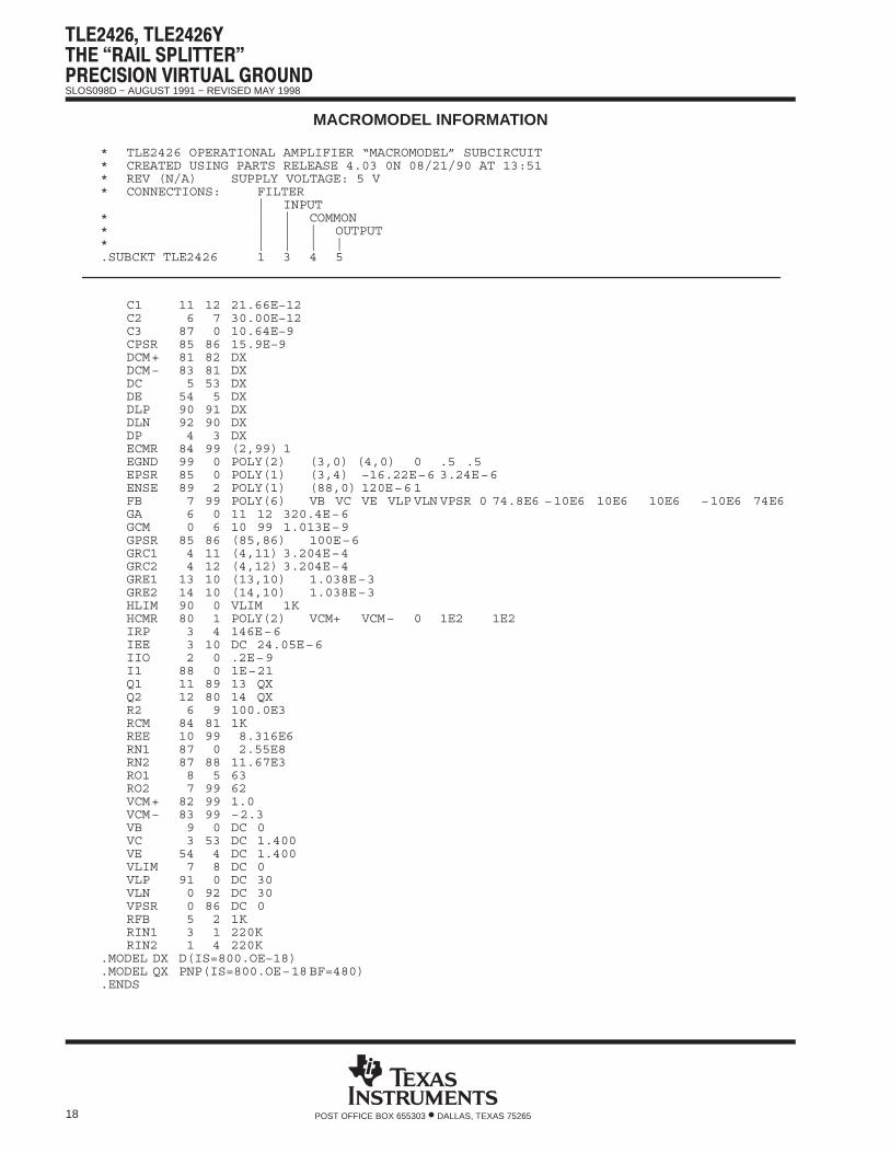
MACROMODEL INFORMATION
* TLE2426 OPERATIONAL AMPLIFIER “MACROMODEL” SUBCIRCUIT* CREATED USING PARTS RELEASE 4.03 0N 08/21/90 AT 13:51* REV (N/A) SUPPLY VOLTAGE: 5 V* CONNECTIONS: FILTER
| INPUT* | | COMMON* | | | OUTPUT* | | | |.SUBCKT TLE2426 1 3 4 5
C1 11 12 21.66E−12C2 6 7 30.00E−12C3 87 0 10.64E−9CPSR 85 86 15.9E−9DCM+ 81 82 DXDCM− 83 81 DXDC 5 53 DXDE 54 5 DXDLP 90 91 DXDLN 92 90 DXDP 4 3 DXECMR 84 99 (2,99) 1EGND 99 0 POLY(2) (3,0) (4,0) 0 .5 .5EPSR 85 0 POLY(1) (3,4) −16.22E−6 3.24E−6ENSE 89 2 POLY(1) (88,0) 120E−61FB 7 99 POLY(6) VB VC VE VLP VLN VPSR 0 74.8E6 −10E6 10E6 10E6 −10E6 74E6GA 6 0 11 12 320.4E−6GCM 0 6 10 99 1.013E−9GPSR 85 86 (85,86) 100E−6GRC1 4 11 (4,11) 3.204E−4GRC2 4 12 (4,12) 3.204E−4GRE1 13 10 (13,10) 1.038E−3GRE2 14 10 (14,10) 1.038E−3HLIM 90 0 VLIM 1KHCMR 80 1 POLY(2) VCM+ VCM− 0 1E2 1E2IRP 3 4 146E−6IEE 3 10 DC 24.05E−6IIO 2 0 .2E−9I1 88 0 1E−21Q1 11 89 13 QXQ2 12 80 14 QXR2 6 9 100.0E3RCM 84 81 1KREE 10 99 8.316E6RN1 87 0 2.55E8RN2 87 88 11.67E3RO1 8 5 63RO2 7 99 62VCM+ 82 99 1.0VCM− 83 99 −2.3VB 9 0 DC 0VC 3 53 DC 1.400VE 54 4 DC 1.400VLIM 7 8 DC 0VLP 91 0 DC 30VLN 0 92 DC 30VPSR 0 86 DC 0RFB 5 2 1KRIN1 3 1 220KRIN2 1 4 220K
.MODEL DX D(IS=800.OE−18)
.MODEL QX PNP(IS=800.OE−18BF=480)
.ENDS
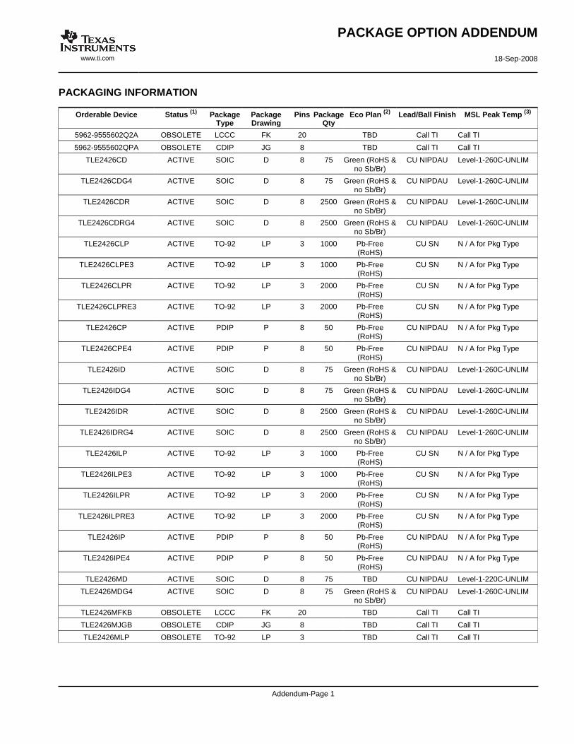
PACKAGING INFORMATION
Orderable Device Status (1) PackageType
PackageDrawing
Pins PackageQty
Eco Plan (2) Lead/Ball Finish MSL Peak Temp (3)
5962-9555602Q2A OBSOLETE LCCC FK 20 TBD Call TI Call TI
5962-9555602QPA OBSOLETE CDIP JG 8 TBD Call TI Call TI
TLE2426CD ACTIVE SOIC D 8 75 Green (RoHS &no Sb/Br)
CU NIPDAU Level-1-260C-UNLIM
TLE2426CDG4 ACTIVE SOIC D 8 75 Green (RoHS &no Sb/Br)
CU NIPDAU Level-1-260C-UNLIM
TLE2426CDR ACTIVE SOIC D 8 2500 Green (RoHS &no Sb/Br)
CU NIPDAU Level-1-260C-UNLIM
TLE2426CDRG4 ACTIVE SOIC D 8 2500 Green (RoHS &no Sb/Br)
CU NIPDAU Level-1-260C-UNLIM
TLE2426CLP ACTIVE TO-92 LP 3 1000 Pb-Free(RoHS)
CU SN N / A for Pkg Type
TLE2426CLPE3 ACTIVE TO-92 LP 3 1000 Pb-Free(RoHS)
CU SN N / A for Pkg Type
TLE2426CLPR ACTIVE TO-92 LP 3 2000 Pb-Free(RoHS)
CU SN N / A for Pkg Type
TLE2426CLPRE3 ACTIVE TO-92 LP 3 2000 Pb-Free(RoHS)
CU SN N / A for Pkg Type
TLE2426CP ACTIVE PDIP P 8 50 Pb-Free(RoHS)
CU NIPDAU N / A for Pkg Type
TLE2426CPE4 ACTIVE PDIP P 8 50 Pb-Free(RoHS)
CU NIPDAU N / A for Pkg Type
TLE2426ID ACTIVE SOIC D 8 75 Green (RoHS &no Sb/Br)
CU NIPDAU Level-1-260C-UNLIM
TLE2426IDG4 ACTIVE SOIC D 8 75 Green (RoHS &no Sb/Br)
CU NIPDAU Level-1-260C-UNLIM
TLE2426IDR ACTIVE SOIC D 8 2500 Green (RoHS &no Sb/Br)
CU NIPDAU Level-1-260C-UNLIM
TLE2426IDRG4 ACTIVE SOIC D 8 2500 Green (RoHS &no Sb/Br)
CU NIPDAU Level-1-260C-UNLIM
TLE2426ILP ACTIVE TO-92 LP 3 1000 Pb-Free(RoHS)
CU SN N / A for Pkg Type
TLE2426ILPE3 ACTIVE TO-92 LP 3 1000 Pb-Free(RoHS)
CU SN N / A for Pkg Type
TLE2426ILPR ACTIVE TO-92 LP 3 2000 Pb-Free(RoHS)
CU SN N / A for Pkg Type
TLE2426ILPRE3 ACTIVE TO-92 LP 3 2000 Pb-Free(RoHS)
CU SN N / A for Pkg Type
TLE2426IP ACTIVE PDIP P 8 50 Pb-Free(RoHS)
CU NIPDAU N / A for Pkg Type
TLE2426IPE4 ACTIVE PDIP P 8 50 Pb-Free(RoHS)
CU NIPDAU N / A for Pkg Type
TLE2426MD ACTIVE SOIC D 8 75 TBD CU NIPDAU Level-1-220C-UNLIM
TLE2426MDG4 ACTIVE SOIC D 8 75 Green (RoHS &no Sb/Br)
CU NIPDAU Level-1-260C-UNLIM
TLE2426MFKB OBSOLETE LCCC FK 20 TBD Call TI Call TI
TLE2426MJGB OBSOLETE CDIP JG 8 TBD Call TI Call TI
TLE2426MLP OBSOLETE TO-92 LP 3 TBD Call TI Call TI
PACKAGE OPTION ADDENDUM
www.ti.com 18-Sep-2008
Addendum-Page 1
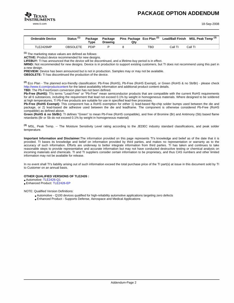
Orderable Device Status (1) PackageType
PackageDrawing
Pins PackageQty
Eco Plan (2) Lead/Ball Finish MSL Peak Temp (3)
TLE2426MP OBSOLETE PDIP P 8 TBD Call TI Call TI
(1) The marketing status values are defined as follows:ACTIVE: Product device recommended for new designs.LIFEBUY: TI has announced that the device will be discontinued, and a lifetime-buy period is in effect.NRND: Not recommended for new designs. Device is in production to support existing customers, but TI does not recommend using this part ina new design.PREVIEW: Device has been announced but is not in production. Samples may or may not be available.OBSOLETE: TI has discontinued the production of the device.
(2) Eco Plan - The planned eco-friendly classification: Pb-Free (RoHS), Pb-Free (RoHS Exempt), or Green (RoHS & no Sb/Br) - please checkhttp://www.ti.com/productcontent for the latest availability information and additional product content details.TBD: The Pb-Free/Green conversion plan has not been defined.Pb-Free (RoHS): TI's terms "Lead-Free" or "Pb-Free" mean semiconductor products that are compatible with the current RoHS requirementsfor all 6 substances, including the requirement that lead not exceed 0.1% by weight in homogeneous materials. Where designed to be solderedat high temperatures, TI Pb-Free products are suitable for use in specified lead-free processes.Pb-Free (RoHS Exempt): This component has a RoHS exemption for either 1) lead-based flip-chip solder bumps used between the die andpackage, or 2) lead-based die adhesive used between the die and leadframe. The component is otherwise considered Pb-Free (RoHScompatible) as defined above.Green (RoHS & no Sb/Br): TI defines "Green" to mean Pb-Free (RoHS compatible), and free of Bromine (Br) and Antimony (Sb) based flameretardants (Br or Sb do not exceed 0.1% by weight in homogeneous material)
(3) MSL, Peak Temp. -- The Moisture Sensitivity Level rating according to the JEDEC industry standard classifications, and peak soldertemperature.
Important Information and Disclaimer:The information provided on this page represents TI's knowledge and belief as of the date that it isprovided. TI bases its knowledge and belief on information provided by third parties, and makes no representation or warranty as to theaccuracy of such information. Efforts are underway to better integrate information from third parties. TI has taken and continues to takereasonable steps to provide representative and accurate information but may not have conducted destructive testing or chemical analysis onincoming materials and chemicals. TI and TI suppliers consider certain information to be proprietary, and thus CAS numbers and other limitedinformation may not be available for release.
In no event shall TI's liability arising out of such information exceed the total purchase price of the TI part(s) at issue in this document sold by TIto Customer on an annual basis.
OTHER QUALIFIED VERSIONS OF TLE2426 :
• Automotive: TLE2426-Q1
• Enhanced Product: TLE2426-EP
NOTE: Qualified Version Definitions:
• Automotive - Q100 devices qualified for high-reliability automotive applications targeting zero defects
• Enhanced Product - Supports Defense, Aerospace and Medical Applications
PACKAGE OPTION ADDENDUM
www.ti.com 18-Sep-2008
Addendum-Page 2
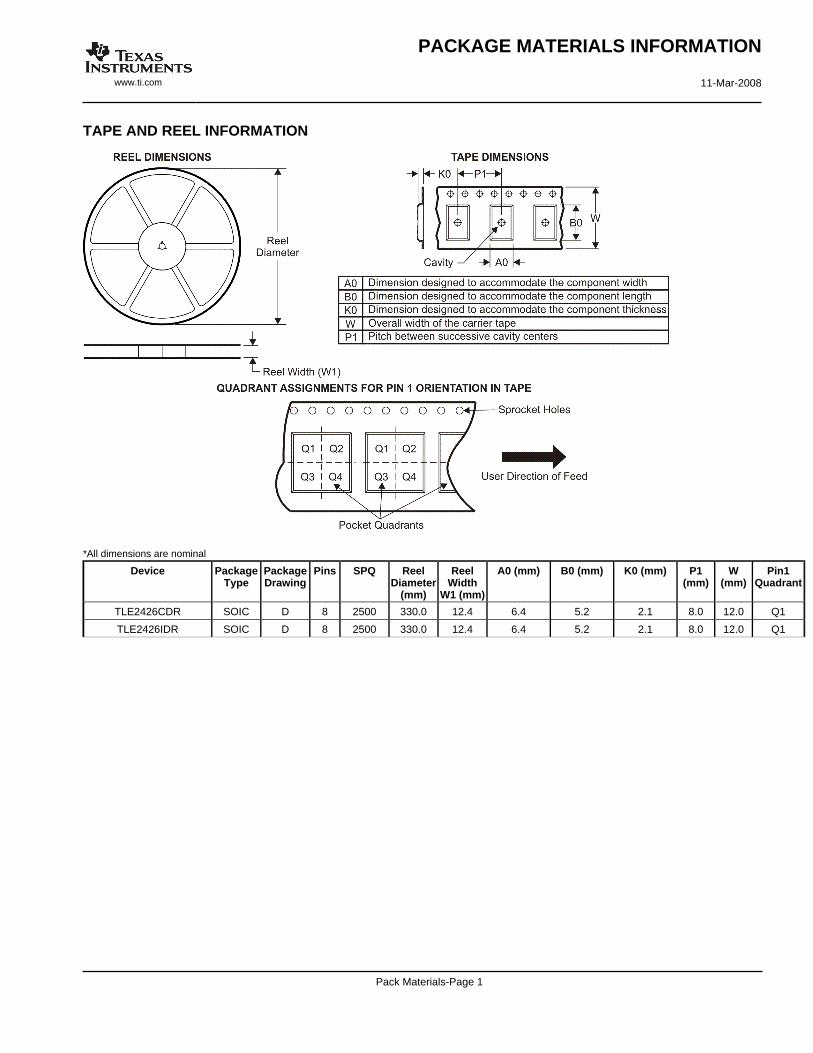
TAPE AND REEL INFORMATION
*All dimensions are nominal
Device PackageType
PackageDrawing
Pins SPQ ReelDiameter
(mm)
ReelWidth
W1 (mm)
A0 (mm) B0 (mm) K0 (mm) P1(mm)
W(mm)
Pin1Quadrant
TLE2426CDR SOIC D 8 2500 330.0 12.4 6.4 5.2 2.1 8.0 12.0 Q1
TLE2426IDR SOIC D 8 2500 330.0 12.4 6.4 5.2 2.1 8.0 12.0 Q1
PACKAGE MATERIALS INFORMATION
www.ti.com 11-Mar-2008
Pack Materials-Page 1
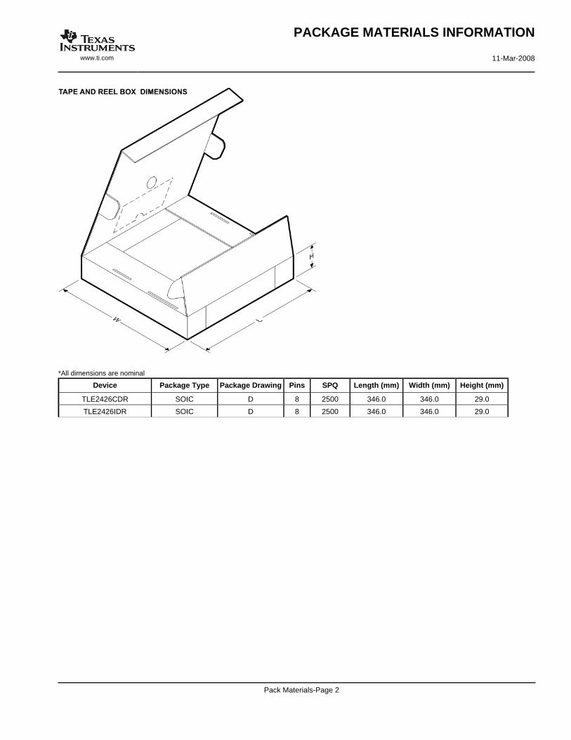
*All dimensions are nominal
Device Package Type Package Drawing Pins SPQ Length (mm) Width (mm) Height (mm)
TLE2426CDR SOIC D 8 2500 346.0 346.0 29.0
TLE2426IDR SOIC D 8 2500 346.0 346.0 29.0
PACKAGE MATERIALS INFORMATION
www.ti.com 11-Mar-2008
Pack Materials-Page 2

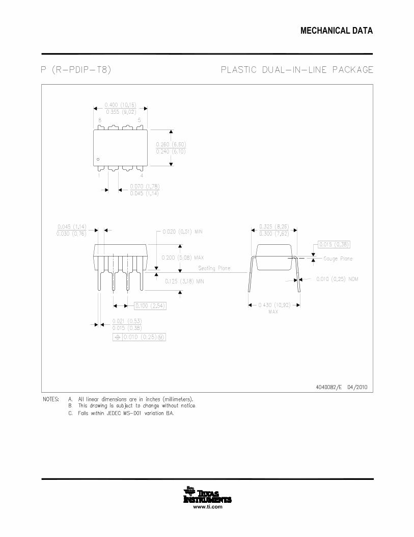
MECHANICAL DATA
MCER001A – JANUARY 1995 – REVISED JANUARY 1997
POST OFFICE BOX 655303 • DALLAS, TEXAS 75265
JG (R-GDIP-T8) CERAMIC DUAL-IN-LINE
0.310 (7,87)0.290 (7,37)
0.014 (0,36)0.008 (0,20)
Seating Plane
4040107/C 08/96
5
40.065 (1,65)0.045 (1,14)
8
1
0.020 (0,51) MIN
0.400 (10,16)0.355 (9,00)
0.015 (0,38)0.023 (0,58)
0.063 (1,60)0.015 (0,38)
0.200 (5,08) MAX
0.130 (3,30) MIN
0.245 (6,22)0.280 (7,11)
0.100 (2,54)
0°–15°
NOTES: A. All linear dimensions are in inches (millimeters).B. This drawing is subject to change without notice.C. This package can be hermetically sealed with a ceramic lid using glass frit.D. Index point is provided on cap for terminal identification.E. Falls within MIL STD 1835 GDIP1-T8


MECHANICAL DATA
MSOT002A – OCTOBER 1994 – REVISED NOVEMBER 2001
1POST OFFICE BOX 655303 • DALLAS, TEXAS 75265
LP (O-PBCY-W3) PLASTIC CYLINDRICAL PACKAGE
4040001-2/C 10/01
STRAIGHT LEAD OPTION
0.016 (0,41)
0.014 (0,35)
0.157 (4,00) MAX
FORMED LEAD OPTION
0.104 (2,65)
0.210 (5,34)0.170 (4,32)
0.050 (1,27)
0.016 (0,41)
0.022 (0,56)
0.500 (12,70) MIN
SeatingPlane
0.175 (4,44)0.205 (5,21) 0.165 (4,19)
0.125 (3,17)DIA
D
C
0.105 (2,67)0.095 (2,41)
0.135 (3,43) MIN
0.080 (2,03)
0.055 (1,40)0.045 (1,14)
1
0.105 (2,67)
2 3
0.080 (2,03)0.105 (2,67)
NOTES: A. All linear dimensions are in inches (millimeters).B. This drawing is subject to change without notice.
C. Lead dimensions are not controlled within this area
D. FAlls within JEDEC TO -226 Variation AA (TO-226 replaces TO-92)E. Shipping Method:
Straight lead option available in bulk pack only.Formed lead option available in tape & reel or ammo pack.
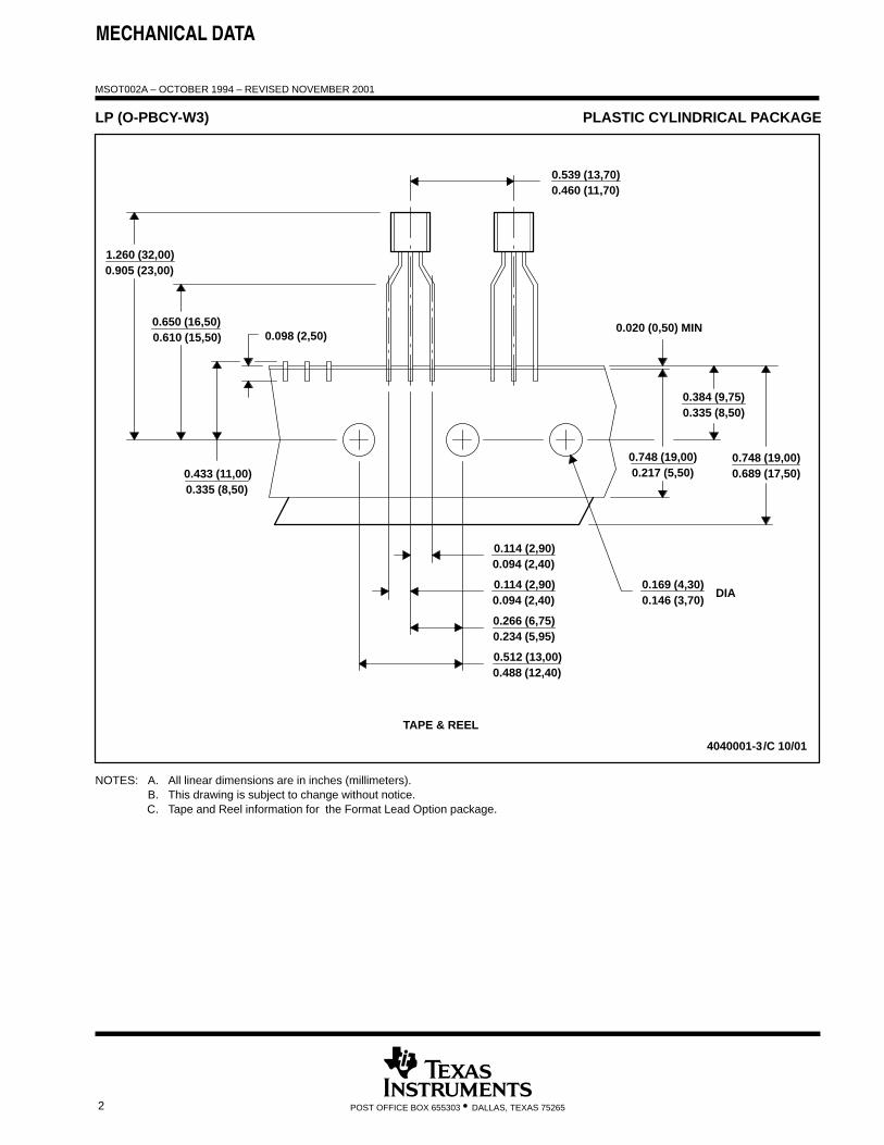
MECHANICAL DATA
MSOT002A – OCTOBER 1994 – REVISED NOVEMBER 2001
2 POST OFFICE BOX 655303 • DALLAS, TEXAS 75265
LP (O-PBCY-W3) PLASTIC CYLINDRICAL PACKAGE
4040001-3/C 10/01
0.094 (2,40)0.114 (2,90)
0.460 (11,70)0.539 (13,70)
TAPE & REEL
0.335 (8,50)0.384 (9,75)
0.020 (0,50) MIN
0.217 (5,50)0.748 (19,00) 0.748 (19,00)
0.689 (17,50)
0.098 (2,50)
0.433 (11,00)0.335 (8,50)
0.610 (15,50)0.650 (16,50)
1.260 (32,00)0.905 (23,00)
0.234 (5,95)0.266 (6,75)
0.512 (13,00)0.488 (12,40)
0.114 (2,90)0.094 (2,40) 0.146 (3,70)
0.169 (4,30)DIA
NOTES: A. All linear dimensions are in inches (millimeters).B. This drawing is subject to change without notice.C. Tape and Reel information for the Format Lead Option package.
IMPORTANT NOTICE
Texas Instruments Incorporated and its subsidiaries (TI) reserve the right to make corrections, modifications, enhancements, improvements,and other changes to its products and services at any time and to discontinue any product or service without notice. Customers shouldobtain the latest relevant information before placing orders and should verify that such information is current and complete. All products aresold subject to TI’s terms and conditions of sale supplied at the time of order acknowledgment.
TI warrants performance of its hardware products to the specifications applicable at the time of sale in accordance with TI’s standardwarranty. Testing and other quality control techniques are used to the extent TI deems necessary to support this warranty. Except wheremandated by government requirements, testing of all parameters of each product is not necessarily performed.
TI assumes no liability for applications assistance or customer product design. Customers are responsible for their products andapplications using TI components. To minimize the risks associated with customer products and applications, customers should provideadequate design and operating safeguards.
TI does not warrant or represent that any license, either express or implied, is granted under any TI patent right, copyright, mask work right,or other TI intellectual property right relating to any combination, machine, or process in which TI products or services are used. Informationpublished by TI regarding third-party products or services does not constitute a license from TI to use such products or services or awarranty or endorsement thereof. Use of such information may require a license from a third party under the patents or other intellectualproperty of the third party, or a license from TI under the patents or other intellectual property of TI.
Reproduction of TI information in TI data books or data sheets is permissible only if reproduction is without alteration and is accompaniedby all associated warranties, conditions, limitations, and notices. Reproduction of this information with alteration is an unfair and deceptivebusiness practice. TI is not responsible or liable for such altered documentation. Information of third parties may be subject to additionalrestrictions.
Resale of TI products or services with statements different from or beyond the parameters stated by TI for that product or service voids allexpress and any implied warranties for the associated TI product or service and is an unfair and deceptive business practice. TI is notresponsible or liable for any such statements.
TI products are not authorized for use in safety-critical applications (such as life support) where a failure of the TI product would reasonablybe expected to cause severe personal injury or death, unless officers of the parties have executed an agreement specifically governingsuch use. Buyers represent that they have all necessary expertise in the safety and regulatory ramifications of their applications, andacknowledge and agree that they are solely responsible for all legal, regulatory and safety-related requirements concerning their productsand any use of TI products in such safety-critical applications, notwithstanding any applications-related information or support that may beprovided by TI. Further, Buyers must fully indemnify TI and its representatives against any damages arising out of the use of TI products insuch safety-critical applications.
TI products are neither designed nor intended for use in military/aerospace applications or environments unless the TI products arespecifically designated by TI as military-grade or "enhanced plastic." Only products designated by TI as military-grade meet militaryspecifications. Buyers acknowledge and agree that any such use of TI products which TI has not designated as military-grade is solely atthe Buyer's risk, and that they are solely responsible for compliance with all legal and regulatory requirements in connection with such use.
TI products are neither designed nor intended for use in automotive applications or environments unless the specific TI products aredesignated by TI as compliant with ISO/TS 16949 requirements. Buyers acknowledge and agree that, if they use any non-designatedproducts in automotive applications, TI will not be responsible for any failure to meet such requirements.
Following are URLs where you can obtain information on other Texas Instruments products and application solutions:
Products Applications
Audio www.ti.com/audio Communications and Telecom www.ti.com/communications
Amplifiers amplifier.ti.com Computers and Peripherals www.ti.com/computers
Data Converters dataconverter.ti.com Consumer Electronics www.ti.com/consumer-apps
DLP® Products www.dlp.com Energy and Lighting www.ti.com/energy
DSP dsp.ti.com Industrial www.ti.com/industrial
Clocks and Timers www.ti.com/clocks Medical www.ti.com/medical
Interface interface.ti.com Security www.ti.com/security
Logic logic.ti.com Space, Avionics and Defense www.ti.com/space-avionics-defense
Power Mgmt power.ti.com Transportation and www.ti.com/automotiveAutomotive
Microcontrollers microcontroller.ti.com Video and Imaging www.ti.com/video
RFID www.ti-rfid.com Wireless www.ti.com/wireless-apps
RF/IF and ZigBee® Solutions www.ti.com/lprf
TI E2E Community Home Page e2e.ti.com
Mailing Address: Texas Instruments, Post Office Box 655303, Dallas, Texas 75265Copyright © 2011, Texas Instruments Incorporated