tk50 tape drive subsystem - t e x t f i l e s d o t c o m tape drive subsystem technical manual e...
TRANSCRIPT

E K-OTK50-TM-O02
TK50 Tape Drive Subsystem
Technical Manual

E K-OTKSO-TM-002
TK50 Tape Drive
Subsystem
Technical Manual
Prepared by Educational Services of
Digital Equipment Corporation
1st Edition, July 1985 2nd Edition, July 1986
Copyright ~1985, 1986 by Digital Equipment Corporation. All Rights Reserved. Printed in U.S.A.
The reproduction of this material, in part or whole, is strictly prohibited. For copy information, contact the Educational Services Department, Digital Equipment Corporation, Maynard, Massachusetts 01754.
The information in this document is subject to change without notice. Digital Equipment Corporation assumes no responsibility for any errors that may appear in this document.
CompacTape is a shared trademark of Digital Equipment Corporation and Minnesota Mining and Manufacturing Company.
Mate-N-Lok is a trademark of AMP, Inc.
Legal Notice TMSCP and STI protocols and documentation are the proprietary information of Digital Equipment Corporation. UNIBUS/Q-BUS/BI-BUS port drivers and documentation for MSCP/TMSCP products are also proprietary information of Digital Equipment Corporation.
The following are trademarks of Digital Equipment Corporation, Maynard, Massachusetts.
mamaDmDTM DECwriter p/as UNIBUS DEC DIGITAL Professional VAX DECmate .LA Rainbow VMS DEC net MASSBUS RSTS VT DECUS PDP RSX Work Processor
CHAPTER 1
1.1 1.2 1.3
CHAPTER 2
2.1 2.2 2.2.1 2.3 2.4 2.5 2.5.1 2.5.2 2.6 2.7 2.7.1 2.7.2 2.7.3 2.7.4 2.7.4.1 2.7.4.2 2.7.4.3 2.7.5 2.7.6 2.7.7 2.7.8 2.7.9 2.7.10 2.7.11 2.7.12 2.7.13
2.7.14 2.7.15 2.8 2.9
CONTENTS
INTRODUCTION AND SPECIFICATIONS
General •••••••••••••••••••••••••••••••••••••••••••• 1-1 TK50 Tape Drive Unit Specifications •••••••••••••• 1-2 Drive to Controller Interface Specifications ••••••• 1-3
DRIVE UNIT DESCRIPTION
General •••••••••••••••• unit Designations •••••••••
Drive Unit variations ••• Cab1 i ng •••••••••••••••••••
. . . . . . . . . . . . . . . . . . . . . . . . . . . . . . . . .2-1 .2-1
••••• 2-1 ••••• 2-2
Power •••••••••••••••••••••••••••••••••••••••••••••• 2-3 Physical Description ••••••••••••••••••••••••••••••• 2-3
Drive Board •••••••••••••••••••••••••••••••••••••• 2-4
. . . . . . . . . . . . . . . . . . . . . . . . . . . ••••• 2-5 • •••• 2-6 ••••• 2-6
Tape Transport (Figure 2-4) Controls and Indicators ••• Drive Board Description •••
Write Data Chain •••••••• . ..................... . 2-7 Wr i te Erase •••••••••••••••••••••••••••••••••••••• 2-8 Write Head Selection..................... • •••• 2-8 DC Low Circui t (Sheet 2). • ••••••••••••••••••• 2-8
+12 Volt Path ••••••••••••••••••••••••.••••••••• 2-8 +5 Volt Path ••••••••••••••••••••••••••••••••••• 2-9 Low Voltage Effect ••••••••••••••••••••••••••••• 2-9
DAC Reference Voltage Generation Circuit ••••••••• 2-9 Automatic Gain Control (AGC) Circuit (Sheet 2) •• 2-10 Read Head Select Circuitry (Sheet 2) •••••••••• 2-10 Read Amplifier Circuit (Sheet 2) •••••••••••••••• 2-11 Phase Lock Loop Circuit (Sheet 4) ••••••••••••••• 2-12 Pump Down Circuit ••••••••••••••••••••••••••••••• 2-13 Pump Up Circuit ••••••••••••••••••••••••••••••••• 2-13 VCO Generation •••••••••••••••••••••••••••••••••• 2-14 Pump Up and Pump Down Signal Generation (Sheet 4) ••••••••••••••••••••••••••••••••••••••• 2-15 Data Detection •••••••••••••••••••••••••••••••••• 2-16 Drive Commands and Status ••••••••••••••••••••••• 2-16
Tape Hub (Refer to Figures 2-4 and 5-4) ••••••••••• 2-16 Link Arms ••••••••••••••••••••••••••••••••••••••••• 2-16
iii

2.10 2.11 2.12 2.13 2.14 2.15 2.16 2.17 2.18 2.19 2.19.1 2.19.2 2.19.2.1 2.19.2.2 2.20 2.21 2.21.1 2.21.1.1 2.21.1.2 2.21.1.3 2.21.1.4 2.21.1.5 2.21.2
CHAPTER 3
3.1 3.2 3.3 3.4 3.4.1 3.4.2 3.5 3.6 3.6.1 3.6.2 3.6.3
Tape Cartridge Insertion.................. • ••••• 2-17 Tape Load to Beginning of Tape (BOT) •••••••••••• 2-17 Tape Motion ••••••••••••••••••••••••••••••••••••••• 2-17 Read/Write Head ••••••••••••••••••••••••••••••••••• 2-18 Initialization: Writing and Reading CALTRACKS ••••• 2-18 Writing Data (Figures 2-7 and 2-8) •••••••••••••••• 2-19 Differential Signal Pair Description •••••••••••••• 2-22 Signal Interface Timing ••••••••••••••••••••••••••• 2-22 Serial Controller to Drive Communications ••••••••• 2-25 Basic Controller/Drive Communications Protocol •••• 2-26
Controller-to-Drive Command Protocol •••••••••••• 2-26 Drive-to-Controller status Protocol ••••••••••••• 2-26
Change of Drive State ••••••••••••••••••••••••• 2-26 Drive Detected Errors. • •••••••••••••••••• 2-26
TK50 Commands ••••••••••••••••••••••••••••••••••••• 2-27 TK50 Drive States ••••••••••••••••••••••••••••••••• 2-28
Drive State Status •••••••••••••••••••••••••••••• 2-28 Done (40)............................... • ••• 2-29 Enable Write Gate (50) •••••••••••••••••••••••• 2-29 Dropout Sensed (60) ••••••••••••••••••••••••••• 2-29 Track Boundary (70) ••••••••••••••••••••••••••• 2-29 Load/Run State Change (Table 2-6)..... • •••• 2-29
Drive Error Status •••••••••••••••••••••••••••••• 2-30
OPERATION PROCEDURES
Introduction •.••••••••••••••••••••••••••••••••••••• 3-1 About the Tape Cartridge ••••••••••••••••••••••••••• 3-2 Terms Used in this Chapter ••••••••••••••••••••••••• 3-2 Inspecting and Loading a Tape Cartridge •••••••••• 3-4
A Running TK50.......................... • •••• 3-14 Lights................................... • •••• 3-14
Unloading the Tape •••••••••••••••••••••••••••••••• 3-15 TK50 Applications...................... • •••••• 3-19
As a Back-Up Device ••••••••••••••••••••••••••••• 3-19 As a Software Distribution Medium ••••••••••••••• 3-19 As a "Journaling" Device •••••••••••••••••••••••• 3-19
iv

CHAPTER 4
4.1 4.2 4.2.1
4.2.2 4.2.3 4.2.4 4.2.5 4.2.6
4.2.7 4.2.S 4.2.9 4.2.10 4.2.11 4.2.12 4.2.13 4.2.14 4.2.15 4.2.16 4.2.17 4.2.1S 4.2.19 4.2.20 4.2.21 4.2.22 4.2.23 4.2.24 4.2.25 4.2.26 4.2.27 4.2.2S 4.2.29 4.2.30 4.2.31 4.2.32 4.2.33 4.2.34 4.2.35 4.2.36 4.2.37 4.2.3S 4.2.39 4.2.40 4.2.41 4.2.42 4.3
DRIVE UNIT REPAIR
General •••••••••••••••••••••••••••••••••••••••••••• 4-1 Error Codes •••••••••••••••••••••••••••••••••••••••• 4-1
Failure to Load to Beginning of Tape (BOT - - (S1 H) •••••••••••••••••••••••••••••••••••• 4-1 Failure to Load Tape into Cartridge (S2H) •••••••• 4-2 General Motor or Tachometer Failure (S3H) •••••••• 4-2 Motor A Failure (Supply Motor) -- (S4H) •••••••••• 4-3 Motor B Failure (Take-up Motor) -- (S5H) ••••••••• 4-3 Drive Lost Control of Tape or Bad Tachometer -- (86H) ••••••••••••••••••••••••••••••••••••••••• 4-4 Excessive Drag in Tape Transport -- (S7H) •••••••• 4-4 Failure to Stop Tape or Remain Stopped -- (SSH) •• 4-5 Cartridge Insert Error -- (S9H) •••••••••••••••••• 4-5 Cartridge Extract Error -- (SAH) ••••••••••••••••• 4-6 Move Error -- (SBH) •••••••••••••••••••••••••••••• 4-6 Deceleration Error -- (SCH) •••••••••••••••••••••• 4-7 Reel Error -- (SDH) •••••••••••••••••••••••••••••• 4-7 Check Byte Error -- (SEH) •••••••••••••••••••••••• 4-7 Unload Error -- (SFH) •••••••••••••••••••••••••••• 4-S S155 Memory Error -- (90H) ••••••••••••••••••••••• 4-S S155 Timer Error -- (91H) •••••••••••••••••••••••• 4-S Read Head 1 Error -- (92H) ••••••••••••••••••••••• 4-9 Read Head 2 Error -- (9 3H) ••••••••••••••••••••••• 4- 9 Cartridge Insert/Extract Error -- (94H) ••••••••• 4-10 EOT Sensed in Read/Write/Seek State -- (95H) •••• 4-10 BOT Sensed in Read/Write/Seek State -- (96H) •••• 4-11 Address Overflow Error -- (97H) ••••••••••••••••• 4-11 Address Underflow Error -- (9SH) •••••••••••••••• 4-12 Servo Error -- (99H) •••••••••••••••••••••••••••• 4-12 Failure in Tracking -- (9AH) •••••••••••••••••••• 4-12 Command Error (9BH) ••••••••••••••••••••••••••••• 4-13 Illegal Command -- (9CH) •••••••••••••••••••••••• 4-13 Write Lock Error -- (9DH) ••••••••••••••••••••••• 4-13 Write Gate Signal Timing Error -- (9EH) ••••••••• 4-14 No Write Gate Error -- (9FH) •••••••••••••••••••• 4-14 Error Sensing CALTRACK1 -- (AOH) •••••••••••••••• 4-15 Error Sensing CALTRACK2 -- (A1H) •••••••••••••••• 4-15 CALTRACK1 Error -- (A2H) •••••••••••••••••••••••• 4-16 CALTRACK2 Error -- (A3H) •••••••••••••••••••••••• 4-16 CALTRACK2 Offset Error -- (A4H) ••••••••••••••••• 4-17 Tape Edge Error -- (A5H) •••••••••••••••••••••••• 4-17 Top Tape Edge Tolerance Error -- (A6H) •••••••••• 4-1S Drive is Overheating -- (A7H) ••••••••••••••••••• 4-1S BOT Sensor Error -- (ASH) ••••••••••••••••••••••• 4-lS No Hall Switch Signals -- (A9H) ••••••••••••••••• 4-19 No Tachometer Pulses Present -- (AAH) ••••••••••• 4-19
Subassembly Removal and Replacement Procedures •••• 4-20
v

4.3.1 4.3.2 4.3.3 4.3.4 4.3.5 4.3.6 4.3.7 4.3.8 4.3.9 4.3.10
CHAPTER 5
5.1 5.2 5.2.1 5.2.2 5.2.3 5.2.4 5.2.5 5.2.5.1 5.2.5.2 5.2.5.3 5.2.6 5.2.6.1 5.2.6.2 5.3 5.3.1 5.3.2 5.3.3 5.4 5.4.1 5.4.1.1 5.4.1.2 5.4.1.3 5.4.1.4 5.4.1.5 5.4.1.6 5.4.1.7 5.4.1.8 5.4.2 5.4.2.1 5.4.2.2 5.4.2.3 5.4.2.4 5.4.2.5 5.4.2.6
5.4.2.7
Drive Board Removal ••••••••••••••••••••••••••••• 4-20 Front Bezel Remova1 ••••••••••••••••••••••••••••• 4-21 Read/Write Head Bracket Assembly Remova1 •••••••• 4-21 Tachometer Removal.................... • •••• 4-22 Solenoid/Interposer Removal ••••••••••••••••••••• 4-22 Take-up Motor (Motor A) Removal ••••••••••••••••• 4-22 Stepper Motor Removal..... ••••••••• • •••• 4-23 Heat Sensor Removal •••••••••••••••••••••• ••••• 4-23 Supply Motor Removal •••••••••••••••••••••••••• 4-24 Receiver Assembly Removal ••••••••••••••••••••••• 4-24
TQK50 CONTROLLER THEORY OF OPERATION
Ge ne r a 1 •••••••••••••••••••••••••••••••••••••••••••• 5-1 The 80186 Microprocessor ••••••••••••••••••••••••••• 5-3
Power-up Reset ••••••••••••••••••••••••••••••••••• 5-3 Microprocessor Cycle Time.................. • •• 5-4 Memory Chip Select Lines ••••••••••••••••••••••••• 5-4 Peripheral Chip Select Lines ••••••••••••••••••••• 5-5 Interrupts •••.•••••••••.•••••••••••••••••••• ••••• 5-6
• •• 5-6 MPSC Interrupts........ • •••••••• FPLS Interrupts ••••••••••••••••••••• . .... . 5-6 Nonmaskable Interrupt (NMI) •••••••••••••• • ••• 5-6
DMA Operations....... • ••••••••••••• ..... . 5-7 DMA Wri te. • • • • • • • • • • ••••• • •• 5-7 DMA Read........... • ••••• • •• 5-7
Memory •••••••••••••.••• . . . . . . . . . . . . . . . . . . . . . . . • •• 5-7 EPROM •••••••••••••••••••••••••••••••••••••••••••• 5-7 Data Transceivers •••••••••••••••••••••••••••••••• 5-8 RAM. • • • • • • • • • • • • • • • • • • • • • • • • • • • • • • • • • • • • • • •••• 5-8
Control and Status Registers............... • •••• 5-9 Miscellaneous Control Register........... • •••• 5-9
Drive Erase (High True) ••••••••••••••••••••••• 5-10 Drive Write Gate (High True) •••••••••••••••••• 5-10 Enable Gap Detect (High True) ••••••••••••••••• 5-10 Clear SA Initialization (High True) ••••••••••• 5-10 Clear IP Initialization (High True) ••••••••••• 5-11 Diagnostic Mode (High True) ••••••••••••••••••• 5-11 Reset LED 1 (High True) ••••••••••••••••••••••• 5-11 Reset LED 2 (High True) ••••••••••••••••••••••• 5-11
Unit Number and Status Register ••••••••••••••••• 5-12 SA Write Initialization (High True) -- DATAO •• 5-l2 IP Read Initialization (High True) -- DATA1 ••• 5-12 Drive Erase (Low True) -- DATA2 ••••••••••••••• 5-l2 Drive Write Gate (Low True) -- DATA3 •••••••••• 5-l2 Q-bus Interrupt Request (Low True) -- DATA4 ••• 5-13 Q-bus Interrupt Request Done (Low True) -- DATA5 ••••••••••.••••••••••••••••••••••••••• 5-13 Q-bus Memory Parity Error (Low True) -- DATA6 ••••.•••••••.••••••••••••••••••••••••• 5-13
vi

5.4.2.S 5.4.2.9 5.4.3 5.4.4 5.4.5 5.4.6 5.4.7 5.4.S 5.4.9 5.5 5.5.1 5.5.1.1 5.5.1.2 5.5.1.3 5.5.2 5.5.3 5.5.4 5.5.5 5.5.5.1 5.5.5.2 5.5.6 5.6 5.6.1 5.6.2 5.7 5.7.1 5.7.2 5.7.3 5.7.4
CHAPTER 6
6.1 6.2 6.3 6.3.1
6.3.2 6.3.3 6.3.3.1 6.3.3.2 6.4 6.5 6.6 6.7 6.7.1 6.7.1.1 6.7.1.2 6.7.1.3
Drive Cable In (High True) -- DATA7 ••••••••••• 5-13 unit Number (High True) DATAS-DATA15 ••••••• 5-13
Vector Register (High True) ••••••••••••••••••••• 5-13 Hardware Revision Register (High True) •••••••••• 5-14 SA Reg ister ••••••••••••••••••••••••••••••••••••• 5-14 I P Re g i s t e r. • • • • • • • • • • • • • • • • • • • • • • • • • • • • • • • • • • • • 5 - 15 Module Starting Addresses/Interrupt Vectors ••••• 5-16 unit Number DIP Switch •••••••••••••••••••••••••• 5-19 Revision Level Switch Pack •••••••••••••••••••••• 5-19
Q22 Bus Interface Logic ••••••••••••••••••••••••••• 5-21 FPLS Control Logic •••••••••••••••••••••••••••••• 5-21
Bus Mastership Acquisition Phase •••••••••••••• 5-21 Data Transfer Phase ••••••••••••••••••••••••••• 5-22 Bus Mastership Relinquish Phase ••••••••••••••• 5-23
Error During Q-bus DMA Transfer ••••••••••••••••• 5-23 FPLS Interrupt •••••••••••••••••••••••••••••••••• 5-24 Q22 Bus Register •••••••••••••••••••••••••••••••• 5-24 DMA Address and Data Registers •••••••••••••••••• 5-25
DMA Address Register ••••.•••.••••••••••••••••• 5-25 DMA Data Register ••••••••••••••.••••••••••••.• 5-25
Q-bus Interrupt Logic ••••••••••••••••••••.•••••• 5-26 Tape Drive Interface •••••••••••.•••••••••••••••••• 5-26
7201 Multi-Protocol Serial Controller (MPSC) •••• 5-26 Differential Drivers and Receivers •••••••••••••• 5-2S
Diagnostic Hardware ••••••••••••••••••••••••••••••• 5-29 Diagnostic Indicators ••••••••••••••••••••••••••• 5-29 Miscellaneous Register Loopback ••••••••••••••••• 5-29 7201 MPSC Diagnostic Loopback ••••••••••••••••••• 5-30 Soft Grounds •••••••••••••••••••••••••••••••••••• 5-31
TUKSO CONTROLLER THEORY OF OPERATION
Ge n era 1 •...•••..••••••••••••.••••.••••..•.•••...••. 6-1 Power-Up Reset (MP-2059, CS, Sheet 1) •••••••••••••• 6-1 Microprocessor Cycle Time (MP-2059, CS, Sheet 2) ••• 6-2
Memory Chip Select Lines (MP-2059, CS, Sheets 2 and 3) ............................•............ 6-2 Peripheral Chip Select Lines ••••••••••••••••••••• 6-3 Peripheral Control Block ••••••••••••••••••••••••• 6-5
Internal and External Interrupts ••••••••••••••• 6-5 Counter/Timers ••••••••••••••••••••••••••••••••• 6-6
DMA Channel (MP-2059, CS, Sheets 2 and 9) •••••••••• 6-7 EPROM (MP-2059, CS, Sheet 3) ••••••••••••••••••••••• 6-7 RAM (MP-2059, CS, Sheet 2) ••••••••••••••••••••••••• 6-S Control and Status Registers ••••••••••••••••••••••• 6-S
Miscellaneous Control Register (Write) ••••••••••• 6-S Drive Erase •••••••••••••••••••••••••••••••••••• 6-9 Drive Write Gate ••••••••••••••••••••••••••••••• 6-9 Enable Gap Detect (Circuit Schematics, Sheet 9) •••••••••••••••••••••••••••••••••••••• 6-10
vii
6.7.1.4 6.7.1.5 6.8 6.9 6.9.1 6.9.2 6.10 6.10.1 6.10.2 6.11 6.11.1 6.11.2 6.11.3
APPENDIX A
APPENDIX B
INDEX
FIGURES
2-1 2-2 2-3 2-4 2-5 2-6 2-7 2-8 2-9 2-10 2-11 3-1 3-2 3-3 3-4 3-5 3-6 3-7 3-8 3-9 3-10 3-11 3-12 3-13 3-14 5-1 5-2 5-3 5-4 6-1 6-2
Diagnostic Mode ••••••••••••••••••••••••••••••• 6-10 Reset LEDs 1-4 •••••••••••••••••••••••••••••••• 6-11
Status Register (Miscellaneous Read Register) ••••• 6-11 Status/Address Reg is ter ••••••••••••••••••••••••••• 6-12
SA Reg ister ••••••••••••••••••••••••••••••••••••• 6-13 IP Register ••••••••••••••••••••••••••••••••••••• 6-13
Tape Drive Interface •••••••••••••••••••••••••••••• 6-14 7201 Multi-Protocol Serial Controller (MPSC) •••• 6-14 Differential Drivers and Receivers •••••••••••••• 6-16
unit Numbering and I/O Addressing ••••••••••••••••• 6-16 Module Starting Addresses/Interrupt Vectors ••••• 6-16 Unit Number Dip Switch (E4, 4-B7) ••••••••••••••• 6-18 Revision Level Dip Switch (E5, 4-C7) •••••••••••• 6-18
TK50 EXPLODED VIEW
TK50 SUBSYSTEM ERROR CODES AND STATUS
System Integrated TK50 ••••••••••••••••••••••••••••• 2-2 Desktop TK50 ••••••••••••••••••••••••••••••••••••••• 2-3 Simplified Logic Diagram: TK50 Tape Drive •••••••••• 2-4 TK50 Tape Drive Transport •••••••••••••••••••••••••• 2-5 TK50 Front View •••••••••••••••••••••••••••••••••••• 2-6 TK50 Rear View ••••••••••••••••••••••••••••••••••••• 2-7 Physical Tape Configuration ••••••••••••••••••••••• 2-20 Recording Direction ••••••••••••••••••••••••••••••• 2-21 Signal I nterf ace Timi ng (A- P) ••••••••••••••••••••• 2- 23 Signal Interface Timing (Q-U) ••••••••••••••••••••• 2-23 Frame Format of Data Coming from Controller ••••••• 2-25 Inspecting Tape Cartridge •••••••••••••••••••••••••• 3-4 Label ing Tape Cartridge •••••••••••••••••••••••••••• 3-5 Write-Protecting Tape •••••••••••••••••••••••••••••• 3-6 Inspecting Leader •••••••••••••••••••••••••••••••••• 3-7 Setting Load/Unload Switch to Unload ••••••••••••••• 3-8 Turning on Power ••••••••••••••••••••••••••••••••••• 3-9 Lifting Cartridge Insert/Release Handle ••••••••••• 3-10 Inserting Tape Cartridge •••••••••••••••••••••••••• 3-11 Lowering Cartridge Insert/Release Handle •••••••••• 3-12 Setting Load/Unload Switch to Load •••••••••••••••• 3-13 Setting Load/Unload Switch to Unload (to Rewind) •• 3-15 Ejecting Tape Cartridge (After Rewind) •••••••••••• 3-16 Removing Tape Cartridge ••••••••••••••••••••••••••• 3-17 Turning Off Power ••••••••••••••••••••••••••••••••• 3-18 TQK50 High Level Block Diagram •••••••••••••••••••• 5-3 Q-bus Timing •••••••••••••••••••••••••••••••••••••• 5-22 Read Data Timing •••••••••••••••••••••••••••••••••• 5-27 TQK50 Detailed Block Diagram •••••••••••••••••••••• 5-32 Power Up Reset Cicuitry •••••••••••••••••••••••••••• 6-2 Microprocessor Timing Circuit (MP-2059, CS, Sheet 2) ........................................... 6-3
viii

6-3
6-4
6-5 6-6 6-7
6-8 A-I
TABLES
1-1 2-1 2-2 2-3 2-4 2-5 2-6 3-1 5-1 5-2 5-3 5-4 5-5 5-6 6-1 6-2 6-3 6-4 6-5 6-6 B-1 B-2 B-3 B-4 B-5 B-6 B-7 B-8
Memory Chip Select Lines (MP-2059, CS, Sheets 2 and 3) ••••••••••••••••••••••••••••••••••••••••••• 6- 3 Peripheral Chip Select Lines (MP-2059, CS, Sheet 2) ••••••••••••••••••••••••••••••••••••••••••• 6-4 FPLS Interrupt (MP-2059, CS, Sheets 2, 4, 6, & 7) •• 6-6 DMA Channel (MP-2059, CS, Sheets 2 and 9) •••••••••• 6-7 Enable Gap Detect Circuit (MP-2059, CS, Sheets 2 and 9) •••••••••••••••••••••••••••••••••••••••••• 6-10 Jumper Settings ••••••••••••••••••••••••••••••••••• 6-17 TK50 Exploded View ••••••••••••••••••••••••••••••••• A-2
TK50 Related Documentation ••••••••••••••••••• ~ ••••• 1-3 TK50 Signal Definition •••••••••••••••••••••••••••• 2-21 Differential Signal Pairs ••••••••••••••••••••••••• 2-22 Signal Interface Timing ••••••••••••••••••••••••••• 2-24 TK50 Commands ••••••••••••••••••••••••••••••••••••• 2-27 Nonerror Drive States ••••••••••••••••••••••••••••• 2-28 Send Status Byte Bit Assignments •••••••••••••••••• 2-29 Light Definitions ••••••••••••••••••••••••••••••••• 3-14 Miscellaneous Control Register Bit Assignments ••••• 5-9 Common Jumper Pack Settings ••••••••••••••••••••••• 5-16 Address/Vector Worksheet •••••••••••••••••••••••••• 5-17 Floating CSR Address Chart •••••••••••••••••••••••• 5-18 Unit Number Switch Pack Settings •••••••••••••••••• 5-20 Revision Level Switch Pack •••••••••••••••••••••••• 5-20 Miscellaneous write Register One (E35) -- PCS5 ••••• 6-9 Miscellaneous write Register Two (E33) -- PCS2 ••••• 6-9 Common Jumper Settings •••••••••••••••••••••••••••• 6-17 Unit Number Switch Pack Settings •••••••••••••••••• 6-18 Revision Level Dip Switch ••••••••••••••••••••••••• 6-19 Revision Level Switch Pack •••••••••••••••••••••••• 6-19 Drive Error Sub-code Values •••••••••••••••••••••••• B-l Controller Internal Status Byte •••••••••••••••••••• B-2 Dr i ve Error Code Byte •••••••••••••••••••••••••••••• B-2 Recoverable Drive Fault Code ••••••••••••••••••••••• B-3 Unrecoverable Drive Faults ••••••••••••••••••••••••• B-4 Drive Flags •••••••••••••••••••••••••••••••••••••••• B-4 U/Q Port Generic SA Error Codes •••••••••••••••••••• B-5 Controller Specific SA Error Codes ••••••••••••••••• B-6
ix

BEFORE YOU START
CHAPTER 1 INTRODUCTION AND SPECIFICATIONS
Generally, this manual is intended for trained Digital service engineers. Chapter 3, Operating Procedures, gives information regarding use of the TK50 Tape Drive. First-time users should also refer to the TK50 Tape Drive Subsystem -User's Guide, EK-OTK50-UG, and the TK50 Tape Drive Subsystem User Reference Card, EK-OTK50-RC.
1.1 GENERAL
The TK50 Tape Drive Subsystem is a mass storage device. It uses removable 94.5M byte tape cartridges to provide backup storage capacity and a software distribution capability for Digital's low-end computer systems.
The subsystem consists of three components: the TK50 Tape Drive, the TK50 Tape Drive Controller, and an interface cable that connects the tape drive to the controller. The TK50 Subsystem may reside entirely within the system unit of a MicroPDP-ll or MicroVAX (I or II); or it can be set up as an external add-on peripheral that can be plugged into other systems, including the PDP/11-23+. The drive unit and the controller are the only field replaceable units (FRUs) in the subsystem.
contain installation or removal and for the two FRUs. Since the TK50 fits a
and is power-plug compatible with the RX50 drives, it may reside in a variety of
It may replace the RX50 in certain
This manual does not replacement procedures 5-1/4 inch footprint and RD50 series disk different systems. configurations.
1-1

Refer to the appropriate system documentation for installation and FRU removal and replacement procedures. For example, if you are troubleshooting a TK50 subsystem problem when the TK50 is in a MicroPDP-11 computer, refer to your MicroPDP-11 System Pocket Service Guide, EK-OLCP5-PS.
NOTE See Chapters 5 and 6 for information about the TK50 controller(s). See Chapters 2 detailed information about streaming tape drive.
detailed Subsystem and 3 for the TK50
The storage medium is a tape cartridge containing a magnetic tape that is 1/2 inch wide and 600 feet long. The tape cartridge is about four by four inches square, and is labeled CompacTape.
1.2 TK50 TAPE DRIVE UNIT SPECIFICATIONS
Tape speed
Bit density
Data rate
Number of tracks
Media type
Capacity
Read/write gap spacing
Recording method
Power required
75 inches per second (in/s)
6667 bits per inch (bits/s)
500 Kbits/s; 45 Kbytes/s
22
Single reel, 1/2 inch, 600 feet long
131 megabytes unformatted, 94.5 megabytes formatted
0.3 inches
MFM, bit serial data, serpentine recording
+5 Vdc, 1.2 amps (typ) , 1.4 amps (max) +12 Vdc, 2.0 amps (typ) , 2.4 amps (max)
1-2

1.3 DRIVE TO CONTROLLER INTERFACE SPECIFICATIONS
Interface type
Connector type
Cable type
Receiver type
Driver type
Differential using RS-422 drivers and receivers
26-pin flat ribbon, polarized; right angle header; PN 12-16832-02
26-wire flat ribbon; PN 17-00034-02; max length 10 ft
AM 26LS32, differential
AM 26LS3l, differential
Table 1-1 TKSO Related Documentation
Title
TKSO-D, -R Tape Drive Subsystem Owner's Manual
TKSO Tape Drive Subsystem User's Guide
TKSO Tape Drive Subsystem User Reference Card
TKSO Tape Drive Subsystem Illustrated Parts Breakdown (IPB)
TKSO Tape Drive Subsystem Field Service Print Set
Order Number
EK-LEPOS-OM
EK-OTKSO-UG
EK-OTKSO-RC
EK-OTKSO-IP
MP-20S4 (drive unit) MP-20SS (M7S46 module) MP-20S9 (M7lS47 module)
1-3
Contents
Provides installation, service, use, and programming information for the desktop and rack-mounted versions of the TKSO.
Provides information on using the TKSO Tape Drive. written for operators with little or no technical background.
Shows how to load and unload a tape cartridge.
Provides an exploded view drawing of the TKSO Tape Drive Subsystem and a comprehensive parts list.
The complete set of prints needed to troubleshoot the TKSO Tape Drive Subsystem to the component level.

CHAPTER 2 DRIVE UNIT
DESCRIPTION
2.1 GENERAL
This chapter provides theory of operation information about the TK50 Tape Drive. The controller(s) to which the drive connects is discussed in succeeding chapters.
Use the block diagrams and mechanical drawings referenced to help you understand the text. For troubleshooting, the Field Service Print Set takes precedence over any block diagrams or mechanical drawings in this book.
This chapter describes how the various components in the TK50 Drive Unit interact during operation. Following the overview theory is more specific information including signal definition and timing, command summary and explanation, and a discussion of the basic drive/controller communications protocol.
Chapter 4 provides the information necessary to remove and replace a subassembly that failed in the drive.
2.2 UNIT DESIGNATIONS
This section lists and describes the unit variations in which the TK50 Tape Drive Subsystem is available.
2.2.1
TK50 TK50-AA TK50-AX TK50-D
TK50-R
Drive Unit Variations
Plain drive, ordered with no system. Single unit in packaging with tape cartridge. Single unit in packaging, no tape cartridge. Desktop version of TK50 external drive version. Rackmount version of TK50 -- external drive version.
2-1

2.3 CABLING
In the system-integrated version of the TK50 (Figure 2-1), the drive and controller both reside in the system box. They are connected with a 26-pin flat ribbon cable, which is in the system box. When the desktop version of the TK50 is used, a shielded external cable connects the TK50 to the system (see Figure 2-2).
The signals on these cables provide serial commands and data sent from the controller to the drive, via differential lines. The drive recognizes the commands and data by interpreting the differences in voltages on the lines. The differential method provides good noise isolation. See Table 2-1 and Sections 2.16 and 2.17 for signal definition, connector pin-outs, and timing diagrams.
Figure 2-1 System Integrated TK50
2-2

2.4
G REEN --___ ~ ..... 'Iii§
LED
CARTRIDGE RELEASE HANDLE
LOAD/UN LOAD SWITCH AND RED LIGHT
Figure 2-2 Desktop TKSO
POWER
SHR-0306-84-8
The TKSO has no internal power supply. The host system must provide the TKSO's required voltages, which are: +12 Vdc at about 2 amps and +S Vdc at about 1 amp. The power connector is the same as the RX and RDSO ser~es floppy diskette drives. The drive uses a 4-pin power plug (PN 12-188SS-00), located at J7 on the drive board, to accept power provided by the host system. If an external TKSO-D, or TKSO-R drive is used, the ac power source should be the same as that used for the host computer.
2.S PHYSICAL DESCRIPTION
The TKSO drive unit consists of two major components: the tape transport and a printed circuit board attached to the bottom of the drive. These two assemblies together are one FRU. The controller that resides in the system backplane is the other FRU.
2-3

2.5.1 Drive Board
The drive board is connected to the bottom of the drive and has discrete analog and digital components.
This module includes an 8751 microprocessor that interprets commands, runs on-board diagnostics, and controls the entire drive operation. The write and read circuits necessary to translate data to and from the MFM format reside on this board. Also included is an 8155 I/O and RAM chip used to sense various conditions, including Beginning of Tape/End of Tape (BOT/EOT), Handle Switch Open/Closed, and Load/Unload Switch Open/Closed. The circuits on this board are detailed as they apply to a specific operation. Figure 2-3 is a simplified block diagram of the entire drive, including the drive board.
VCO EN MISC VCO
SNS 8751 +
CNTRl RD EN DATA SEP
TACH INTO MPU SNS PlS-l
(AMPl, TRACKING)
SER CMD
EN
DUAL DAC
GAP INTI
-l
8155
MPU 8X256 EN RAM
WRT GATE
WRT/ER EN SERVO TIMER
WRT DATA (NRZ)
ENCODE WRT COMP -------------.1 (PAL'S)
ERASE GAP
ONE 'lS 32 QUAD DIFF RECVR
16 MHZ
NRZ RD DATA
RD CLOCK
RD Fil TER'S GAIN CNTRl
SER
STATUS (ECHO)
FWD + BWD CHAN
600+ FEET OF TAPE
MISC SENSE CNTRl
WRT CLOCK
ONE 'lS 31 QUAD DIFF DRVR
SH R-0212-85
Figure 2-3 Simplified Logic Diagram: TK50 Tape Drive
2-4

2.5.2 Tape Transport (Figure 2-4)
The tape drive transport encompasses the mechanical and electromechanical components that allow the TK50 to perform its functions; that is, to read and write data to magnetic tape. These components include: the magnetic read/write head and its stepper motor; the take-up reel and its motor; the tape hub (which serves, effectively, as the supply reel when a tape cartridge is inserted) and its reel motor; and the tachometer, which provides feedback to the 8751 microprocessor regarding tape speed.
LEADER, TAKE-UP
EXTERNAL SHIELD ASSEMBL Y
TACHOMETER ASSEMBL Y
BRACKET & HEAD ASSEMBLY
BASEPLATE & MOTOR ASSEMBLY
TK50 DRIVE MODULE
INSULATOR ASSMEBL Y
REEL, TAKE-UP
CONSTRAINT, TAPE /
/
LEADER
/~~~~~BLY LIN K, BUCKLI NG
REEL, DRIVER
BEZEL ASSEMBLY
Figure 2-4 TK50 Tape Drive Transport
2-5
SH R·0213·85

SHR-0214-85
Figure 2-5 TK50 Front View
2.6 CONTROLS AND INDICATORS
On the front of the TK50 drive is a combination Load/Unload switch and LED indicator (Figure 2-5). When power is applied and a tape cartridge is in place, the Load/Unload switch is used to load the tape for operation. Loading the tape involves coupling two leaders together (one is on the beginning of the tape and the other is part of the drive), then bringing the tape to the Beginning of Tape (BOT) indicator. Unloading the tape involves rewinding to BOT, then unbuckling the two leaders so the tape can seat in the cartridge for removal.
Also on the front of the drive is the cartridge insert/release lever handle. This handle must be raised to insert a tape cartridge, lowered to lock the cartridge in place, and raised to eject a cartridge. The handle must never be raised when the light is on or blinking, or when the system power is off. See Chapter 3 for detailed operator information.
2.7
Refer to Subsystem section.
DRIVE BOARD DESCRIPTION
the drive board schematics in the TK50 Tape Drive Field Service Print Set, MP-2054-CS, while reading this
In the following logic description, the component being described is followed in parentheses by the circuit schematic sheet number and location zone. For example, E13 (1-B8) is in Field Maintenance Print Set MP-2054, Circuit Schematic (CS) sheet 1, location zone 88.
2-6
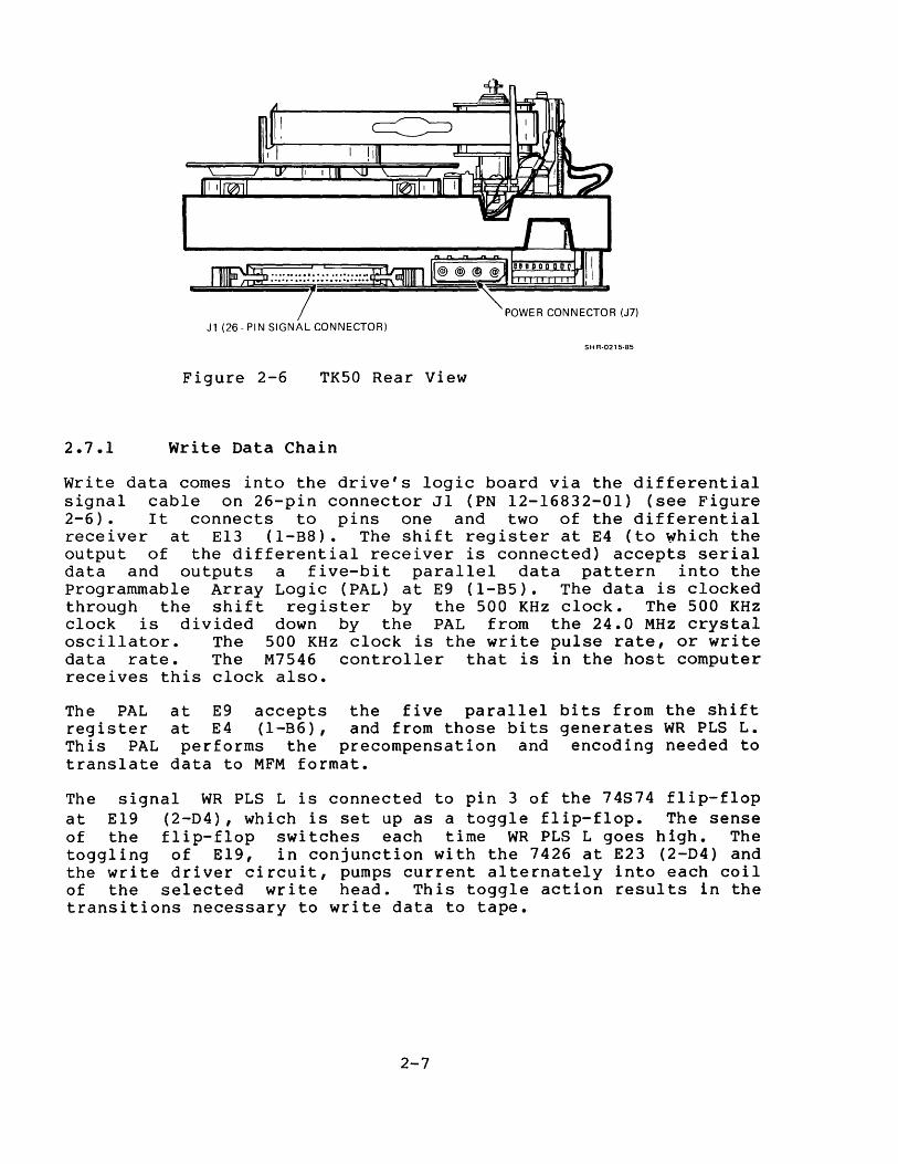
POWER CONNECTOR (J7) Jl (26 - PIN SIGNAL CONNECTOR)
SH R-0215-85
Figure 2-6 TK50 Rear View
2.7.1 Write Data Chain
write data comes into the drive's logic board via the differential signal cable on 26-pin connector Jl (PN 12-16832-01) (see Figure 2-6). It connects to pins one and two of the differential receiver at E13 (1-B8). The shift register at E4 (to which the output of the differential receiver is connected) accepts serial data and outputs a five-bit parallel data pattern into the Programmable Array Logic (PAL) at E9 (1-B5). The data is clocked through the shift register by the 500 KHz clock. The 500 KHz clock is divided down by the PAL from the 24.0 MHz crystal oscillator. The 500 KHz clock is the write pulse rate, or write data rate. The M7546 controller that is in the host computer receives this clock also.
The PAL at E9 accepts the five parallel bits from the shift register at E4 (1-B6), and from those bits generates WR PLS L. This PAL performs the precompensation and encoding needed to translate data to MFM format.
The signal WR PLS L is connected to pin 3 of the 74S74 flip-flop at El9 (2-04), which is set up as a toggle flip-flop. The sense of the flip-flop switches each time WR PLS L goes high. The toggling of El9, in conjunction with the 7426 at E23 (2-04) and the write driver circuit, pumps current alternately into each coil of the selected write head. This toggle action results in the transitions necessary to write data to tape.
2-7

2.7.2 Write Erase
The PAL at E9 controls the write erase function. When the signal WR ERASE L (write erase) is asserted, the PAL shuts off write pulses. Write current, however, is still flowing to the write heads. Therefore, an erase function is performed; that is, write with no data. This function is used to write gaps on tape. When the write erase signal is released, the PAL goes back to MFM encoding and resumes the generation of write pulses.
2.7.3 Write Head Selection
The write heads are selected by the signals WR HD 1 SEL or WR HD 2 SEL (E23 pins 8, 9, 10; pins 11, 12, 13). Head one writes data in the forward direction, head two in the reverse direction.
With the signals HD 1(2) SEL H asserted high, a logic 1 is applied to pin 10 or pin 13 of the 7426 at E23. E23 then outputs a logic 0, which grounds the centertap of the selected write head. Current is then alternately applied to each side of the write head coil, through the transistor pairs at E30 (pins 8, 9, 10 and 12, 13, 14), or E30 (pins 5, 6, 7 and 1, 2, 3), each time the sense of flip-flop E19 switches. This provides a constant current source of 15 milliamps to each write head coil. The alternate application of the current results in the transitions needed to write data to magnetic tape.
2.7.4 DC Low Circuit (Sheet 2)
The DC Low circuit senses a low voltage condition (either +5 or +12 V dropping below their acceptable levels) and shuts down the functions of the tape drive. It shuts down the motor current, resets the 8751 microprocessor at El (1-D6), and disables the write current circuitry.
2.7.4.1 +12 Volt Path -- As long as +12 volts doesn't go below an acceptable level (about 10 V) the transistor at E6 (pins 1, 15, 16
I-AI) is turned on.
If the voltage drops lower than the base-emitter junction voltage of that transistor, E6 (1, 15, 16) turns off. Pin 1 rises, t urn i ng 0 n E 6 ( 6 , 7, 8). Wh e n E 6 (6, 7, 8 ) t urn son, its pin 7 drops, asserting the signal DC LOW L.
A 330 nF capacitor (C47) provides positive feedback and some hysteresis. When DCLOW goes to a logic level 0, the capacitor discharges, dumping some charge back to pin 16 of E6, and turning it off harder. The hysteresis prevents the transistor from oscillating if there is noise at its base (pin 16) when the voltage drops. The hysteresis, then, is to make sure that the DCLOW signal is of a long enough duration.
2-8

Also, as E6 pin I rises (pulled up by Rl9 to +5 V), transistor E6 (pins 2, 3, 4) is turned on and the reset signal R8T H is asserted. The I MF capacitor at C3 (I-A3) discharges. C3 holds the reset line to the 8751 microprocessor asserted on power-up until +5 volts has ramped up completely and cleanly.
2.7.4.2 + 5 Volt Path -- The signal DCLOW is asserted through the same transistor pair as +12 V (E6).
The +5 V low circuit consists essentially of E6 (9, 10, 11) and E6 (12, 13, 14). If +5 V drops lower than about 4.6 V, E6 pin 12, and E6 pin 11 reach about 3.9 V. This asserts DCLOW through E6 ( 1 , 1 5 , 16 ) and E 6 ( 6 , 7, 8).
2.7.4.3 Low Voltage Effect -- When DCLOW is asserted, it places a Iowan the set input of the 74874 flip-flop at E19, pin 10 (2-D4). When the set input is asserted, it causes the flip-flop to assert pin 9 of the PAL at E9. When this pin is asserted, the PAL shuts off the 1 MHz clock.
When the PAL shuts off the 1 MHz clock, it also shuts off the -1.25 reference voltage used by the DACs which drive the reel motors. Regardless of what else happens at this point, the motor current is shut down when the minus voltage reference is removed.
2.7.5 DAC Reference Voltage Generation Circuit
This section explains how the minus reference voltage is generated and how the DACs use that voltage to energize the reel motors.
The minus reference voltage is generated from the 1 MHz clock that originates at pin 17 of the PAL at E9 (1-85).
When the 1 MHz signal rises to about 4 V, it charges capacitor C6 (plus voltage on pin 1, minus voltage on pin 2). When the 1 MHz signal comes down, C6 discharges, and, through diode D5, charges Cll. When the 1 MHz signal goes up again, D5 is reverse biased and Cll holds the charge. This provides a minus 2.1 V constant voltage source at pin 1 of Cll.
The minus voltage source goes to the lK resistor at R3 (3-D6). The diode at D4 develops a -1.25 reference voltage for the multiplying Digital-to-Analog Converter (DAC) at E8 (3-D5). The inputs to the DAC at E8 are the data bus bits from the 8751 microprocessor. The micropocessor selects the DAC, then writes numbers into it, using the data bus. The DAC acts like a programmable current source. Its output current through the op-amps at E16 (3-D3) controls the speed of the reel motors. Thus the microprocessor can speed up or slow down the motors by writing larger or smaller numbers into the DAC.
2-9

The signals Control A and Control B drive the two reel motors (control A for motor A and control B for motor B). These signals are actually connected to three darlington transistors on the motors' printed circuit board. The signals Feedback A and Feedback B are current return signals from the motors that provide a reference to the DAC.
2.7.6 Automatic Gain Control (AGC) Circuit (Sheet 2)
The 4024 at E12 (2-07) binary ripple counter and resistor network (R3l R36) make up a DAC. The existence of the AGC circuit means that the microprocessor has only to set up a value initially by asserting CLR AGC H (E12 pin 2), then applying the signal STP AGC L to step the counter up to the desired gain value.
The gain value is translated to a voltage across R2l (12K) and is applied to the op-amp at E16 (2-C8) (pin 10). The LM324 at E16 (2-C8) compares the gain voltage (set by the microprocessor through E12) to a voltage developed by the intensity with which transistors Q2 and Q3 are turned on. Q2 and Q3 are turned on by developing a voltage across RI04 and Rl05. These voltages are averaged together and then applied to E16 pin 9.
The intensity with which Q2 and Q3 are turned on can be controlled by the op-amp. The output of the op-amp (pin 8) is connected to resistors R94 and R95. The higher the voltage goes, the harder Q2 and Q3 are turned on. This configuration, then, works to control the gain of this pre-amp circuit: The microprocessor clears the counter at E12 and steps it up to a desired gain. The gain value is translated to an analog voltage that is then applied to the op-amp at E16. The output of the op-amp turns Q2 and Q3 on with the appropriate intensity, which results in a value being averaged at the junction of R94 and R95, then applied to pin 9 of the op-amp.
2.7.7 Read Head Select Circuitry (Sheet 2)
The quad-transistor package at E27 (sheet 2 -- lower left) is the read head select circuit. Unlike the write head, the read head coil is not centertapped. E27 (5, 6, 7) and E27 (8, 9, 10) select read head 1; E27 (1, 2, 3) and E27 (12, 13, 14) select read head 2.
The two transistor pairs are biased at different levels, so either one of the pairs may be selected by a single control signal (HD 1 SEL H).
2-10

For example, the bases of the top pair of transistors (read head 1) are set at about 3.1 V and are not switchable. The other pair, though, (head 2) are influenced by the select signal HD SEL 1 H. When HD SEL 1 H is a logic 1, then about 5 V is applied to E27 pin 2 and E27 pin 13. In this case, the top two pairs of transistors are turned on because the emitters of all four transistors are tied together and pulled up to +12 V. If HD 1 SEL H is low, however, the bottom pair of transistors is turned on and head 2 is selected.
2.7.B Read Amplifier Circuit (Sheet 2)
The differential preamplifier circuit feeds into the differential input of the 3470 read amplifier chip at E26 (2-85).
Pins 3 and 4 on the 3470 control the gain of the amplifier. R100 and R101 are controlling the gain of the 3470: if their combined resistance was lower, the gain of the read amplifier would be higher.
The output of the first stage of the 3470 is on pins 16 and 17 (differential output). The read amplifier chip raises the approximately 40 millivolt signal on its inputs (pins 1 and 2) to about 1 V peak-to-peak on each line, or 2 V differential peak-to-peak at ouput pins 16 and 17.
The first stage output is connected to transistors EIB pin 6 and E1B pin 3, and then to inductors L5 and L6. These inductors, along with transistors E1B, form a differentiator circuit.
This differentiator circuit, amplifies The differentiated, passes through a low L2, and C3B.
circuit takes the signal from the 3470 it, and performs a differentiating function. amplified differential analog read signal now pass filter composed of L3, L4, C40, C39, Ll,
The output of the differentiator and filter circuit (ANAl and ANA2) goes back to the 3470 (pins 14 and 15). With the 3470's pins 12 and 13 tied together, this 3470 stage acts like a comparator and is used as a zero crossing detector for peak detection.
The differentiated and filtered signals ANAl and ANA2 are also connected to an amplitude detection circuit consisting of EIB 9, 10, 11; and 12, 13, 14.
The purpose of the 3470 chip is to generate the digital signal RD DATA PLS H. This signal represents the data read from the tape and it consists of a positive pulse for each detected peak.
2-11

Pin 10 of the 3470 (RD DATA PLS H) outputs a 100 ns pulse when a zero-crossing detection is found on its input pins 14 and 15. The position of this pulse represents the timing of the analog peaks that were read from the tape. This raw data is sent to the phase lock loop where the clock signal is recovered and the MFM data is decoded and sent to the controller in the host system via the serial bus.
2.7.9 Phase Lock Loop Circuit (Sheet 4)
The read data pulse from the read amplifier circuit is connected to the PAL at E25 (4-D4) (pin 9) in the phase lock loop circuit. The 500 KHz write clock is also connected to the PAL at E25 (pin 8) •
Whenever there is a gap going into the phase lock loop (a burst of nonexistent or invalid data), the phase lock loop locks in high gain mode on the 500 KHz write clock. This is so the integrating capacitor C25 stays charged nominally, keeping the voltage control oscillator (VCO) running at a nominal frequency. Keeping the integrating cap charged nominally means that not as much correction has to occur when the preamble (first burst of valid data) to the data field comes along.
On the left side of sheet 4, three signals enter the analog circuitry: Pump Up L, Pump Dn L, and RD EN H. The PAL at E29 (4-D7) sources these signals. Pump Up L and Pump Dn L are the phase error correction signals to the charge pump. These signals are in place so that the frequency of the veo can be changed. The signal RD EN H is a gain control signal for the charge pump. It changes the gain of the charge pump to about 5 to 1, so that in high gain mode, there is about five times more current for the corrections than when in low gain mode.
In the gap (and during the early part of the preamble), the phase lock loop is in high gain mode. When in high gain mode, the Read Enable signal is low. When the Read Enable signal goes high, the circuit is in low gain mode. The circuit goes into low gain mode about halfway through the preamble and stays there during the data field.
When the phase lock loop is locked on the 500 KHz clock (write clock) the loop is in high gain mode and RD EN H is low. With RD EN H low, E22 (2,3,4) is turned off. With E22 (2,3,4) turned off, there are two constant current sources providing charge to the loop filter consisting of C24, R53, and C25.
2-12
2.7.10 Pump Down Circuit
When the signal Pump On L goes low, transistor E22 (8,7,6) is turned off, enabling the pump down constant current source.
A resistor-divider network is connected to the base of E22 (11, 10, 9), which produces about 2.9 V at the base of E22 (pin 9). There is a 0.7 V drop across the base-emitter junction of E22, producing about 2.1 V at pin 10. This results in a current through diode 010 and resistors R79 and R83 in high gain mode, and through R79 alone in low gain mode.
The collector of transistor E22 is connected to the filter cap at C25. C25 is the major integrating cap in this circuit. R53 develops the phase correction voltages for the VCo.
So when a pump down occurs (Pump On L goes low), a pump down correction is telling the VCO clock to slow down, through the 74S124 chip at E21. The output of E21 (VCO OUT H) is connected to the clock input of the PAL at E25.
When the Pump On signal is not asserted, E22 (6, 8, 7) turns on, pulling up pin 10, reverse biasing the base-emitter junction of E22 - 10 and 9, and turning the constant current source off.
2.7.11 Pump Up Circuit
The constant current source for the pump up circuit consists of resistors R49 and R50, diodes 07 and 08, and transistor Ql.
A resistor-divider network is connected across the base (pin 1) of transistor Ql. When the Pump Up signal (Pump Up L) is asserted low, it pulls the base of Ql down to about 4.5 V. When the base is pulled to 4.5 V, a drop across the base-emitter junction means that the emitter voltage is about 5.2 V.
At this point, there is 5.2 V on one side of the parallel network (R49, R50, 07, 08) and 12 V on the other side (R49 and R50 pins 2). The current [determined by 6.8 volts across R50 (low gain mode) or that current plus the six volts which is across R43 in high gain mode] goes to the loop filter through the collector at Ql. A pump up correction causes the charge to be dumped into integrating capacitor C25 and develops a phase error correction voltage across R53. Both the charge being dumped and the phase error correction voltage cause the VCO to run faster.
In the case of pump down, the cap at C25 was discharged slightly. In this case, however, C25 is charged slightly.
2-13
2.7.12 veo Generation
The veo E21 (4-C3) chip's output frequency is essentially controlled by the voltage at it's input pin 2. The higher that voltage is, the higher frequency its clock output will be (pin 7).
The circuit that consists of E22 (12, 13, 14) (4-A4), R48, R55, and 09 is a compensation circuit that compensates for differences in VCO chips' center frequencies. It also eliminates the need for adjustments to the frequency-determining capacitor that is part of the VCO circuit.
Optimum range and linearity are achieved by operating the VCO such that the center frequency occurs at 3.2 input volts. To achieve this goal, and to compensate for differences between veo chips, a varactive diode (09) is included in the circuit. This diode adjusts its capacitance based on how much reverse bias voltage is across its capacitor (09).
The 8751 microprocessor sends out the Read Enable control signal (RO EN H) by synchronizing on the occurences of the gap interrupt (the signal GAPL on the microprocessor's input pin 13). When the microprocessor is first locking on the gaps (after the tape has come up to speed), it looks for the assertion of the gap interrupt signal, sets an internal timer running, waits until about halfway through the preamble, then asserts read enable.
When Read Enable is asserted, transistor E22 (2, 3, 4) turns on. When the transistor turns on, it pulls the anode (pin 2) of the lN4l52 diode at 07 (junction of R49) low, and pulls the cathode of 010 and R83 up, so it effectively disconnects R49 and R83 from being part of the network for the pump up and pump down current sources.
On the lower half of the constant current source (010), 2.1 Vare present at the emitter of E22 (pin 10). But instead of 5 milliamps of current from the constant source, there is only about 1 milliamp. This lower current results because the diode 010 and resistor R83 have effectively been eliminated from the circuit. The result is that there is only 1 milliamp of correction current going to the loop filter.
The upper half of the constant current source (07, R49, R50) works much the same way as the lower half; that is, R49 and 07 are effectively out of the circuit, which means that R50 limits the current flowing to about 1 milliamp.
The Read Enable Signal, in addition to being connected to the transistor E22, is also connected to the PAL at E25 (pin 7).
2-14

When the read enable signal is asserted, the phase lock loop circuit is decoding the data, which it knows is all logic Is, in the preamble. When it sees a missing transition in a data cell (a 0), it clocks out that first zero onto the serial bus, through the quad driver at E5 (26LS31). The read clock is also output from this quad driver at the same time. E5 is connected to the differential signal cable that connects to the 7201 chip on the controller.
This zero acts almost like a start bit, in that it informs the 7201 to begin its CRC checking and to start its serial UART. Followed by the zero is the data, the CRC, and the postamble from the phase lock loop circuit.
2.7.13 Pump Up and Pump Down Signal Generation (Sheet 4)
The PAL at E25 (4-D4), in conjunction with the PAL at E29 (4-D7), generates the Pump Up and Pump Down signals. The PAL at E29 is being used as a phase detector.
The PAL at E25 has the 140 ns (approximately) read pulse on its input pin 9. It uses the read pulse, with the VCO clock on its pin 1, to form the load pulse LOAD PLS H •. The load pulse lasts exactly one VCO clock period in duration. The result is one load pulse per read data pulse through the PAL at E25.
This synchronized (in effect) version of the read pulse is connected to the PAL at E29 (pin 6). E29 provides a counting function (CNTO - CNT4) such that each data cell has 16 VCO clocks and each clock cell has 14 VCO clocks. So the data cell has a maximum of eight clocks for pump down and eight clocks for pump up.
If the read data is exactly on time, the load pulse to E29 is at the exact center of the data cell, and no correction needs to be performed. But if the load pulse is early (due, for example, to peak shift), then the VCO clock has to go faster to catch up to the pulse in relation to the data cell. In this case, the PAL asserts the signal Pump Up L. Pump up increases the frequency of the VCO clock. When the center of the cell occurs, the Pump Up signal is withdrawn and the PAL at E29 continues counting.
If the load pulse is late, the counter at E28 gets loaded with the 2's complement of the number of VCO periods for which it was late; then pump down is asserted until the carry signal is asserted.
2-15

2.7.14 Data Detection
When a load pulse occurs in any part of a data cell, it is considered a logical one and is clocked out from the PAL at E25 as a one. Any missing load pulse within a data cell is considered a zero.
2.7.15 Drive Commands and Status
Serial Drive status is sent back to the controller by the microprocessor, via the 26LS3l quad driver at E5 (4-02). Drive status is sent to the 7201 MPSC chip on the controller over the serial bus.
Commands are received by the 8751 microprocessor via the 26LS32 quad receiver at E13 (1-08). Commands are sent over the serial bus from the 7201 MPSC chip on the controller.
Status information is sent back to the controller from the microprocessor's TxD pin. It is usually sent in response to a commmand from the controller which is accepted on pin 10 of the microprocessor. The 8751 in this case is set up similar to a full-duplex UART.
2.8 TAPE HUB (Refer to Figures 2-4 and 5-4)
When the cartridge release handle is lifted, the supply motor's hub is withdrawn (see Figure A-I in Appendix A). The part of the hub containing the teeth mates with the hub in the tape cartridge to align the height of the tape in the drive. This vertical alignment is needed for two reasons:
1. The tape must be at the correct height for the leader in the cartridge to couple with the leader in the drive.
2. The height of the tape must be the same on both the supply reel (tape cartridge) and the take-up reel, because tight tolerances are needed for the read/write heads to correctly access the tracks on the tape.
2.9 LINK ARMS
The link arms to the left and right of the hub align the cartridge horizontally in the drive. Horizontal alignment is neeeded to make sure that the cartridge cannot shift forward or backward.
The handle mechanism controls both the tape hub and link arms.
2-16
2.10 TAPE CARTRIDGE INSERTION
As the cartridge is inserted, the door on the cartridge opens, exposes the leader mechanism, and then swings out of the way. Two plastic arms are used as guides to mate the supply leader with the take-up leader.
When the cartridge is completely inserted, the interposer is released, locking the cartridge into the drive. The front reel lock inside the cartridge is now also released. The rear reel lock is held until the handle is lowered. As the handle lowers, the tape hub moves to mate with the cartridge and provide vertical tension. At the same time, the link arms move into place to provide horizontal stability to the cartridge.
2.11 TAPE LOAD TO BEGINNING OF TAPE (BOT)
The next operation is to instruct the tape drive to load the tape to the BOT hole. To do this, press and lock the Load/Unload switch on the front right side of the drive. (See also the TK50 Tape Drive Subsystem User's Guide, EK-OTK50-UG.) Pushing in the switch informs the drive to move the tape from the load point (where the leaders couple) to the BOT marker. The 8155 senses both the Load/Unload switch closing and when the tape reaches BOT. When the 8155 senses BOT it informs the controller, through the 8751, that the drive is on-line and ready for use.
2.12 TAPE MOTION
The tachometer senses tape motion. The tachometer consists of a capstan and a finely etched disk. The rear portion of the tachometer has an LED and phototransistor that senses the holes in the etched disk. The capstan and the disk spin as the tape moves across the capstan. In this way, the tachometer can sense the speed of the tape.
The 8751 controls all tape speed and tensioning. The TK50 does not use any driven capstans or air bearings. The tachometer provides all feedback regarding tape speed to the 8751. Tach pulses are connected to the 8155 via one of its I/O Ports.
The tachometer (tach) has a sensor on a phototransistor to tell the microprocessor that the tach is working correctly. The feedback loop from the tach is tested as part of the power-up diagnostics.
The tape moves forward to BOT at about six inches per second under about three ounces of tension. When the tape reaches BOT, the 8155 informs the 8751, which then informs the controller that it is ready for use. The controller responds by telling the drive to complete the initialization.
2-17

2.13 READ/WRITE HEAD
The read/write head consists of four cores: a read core and write core for the forward direction, and a read and write core for the reverse direction. The write cores are 18 mils wide and the read cores are 8 mils wide.
The different track read (8 It allows for media, and it either side, to
widths between the track written (18 mils) and the mils) give the read core more leeway to read data. easier recovery from soft errors inherent in tape also provides the flexibility to move slightly to
compensate for defects in the tape.
The four cores are physically on one head mechanism. The head is driven by a 1 mil per step stepper motor and is held in contact with the stepper by two springs around the head carriage.
2.14 INITIALIZATION: WRITING AND READING CALTRACKS
The next step is for the head to read or write/read calibration tracks 1 and 2 (CALTRACKI and CALTRACK2). The controller sends a command to write and read the CALTRACKS.
If the cartridge has never been used, the following sequence takes place.
1. The drive tries to find and read CALTRACKS 1 and 2. Finding neither, it decides that this is a new cartridge.
2. The head seeks to the top of the tape.
3. Once at the top, the head moves down about 0.2 inches.
4. The write core writes a data burst (CALTRACK 1) in the forward direction.
5. The read core immediately reads CALTRACKI. This is called a read-after-write operation. The read core lags the write core by 0.3 inches, so a slight delay is to be expected before the CALTRACK is read back.
6. The head performs the same operation in the reverse direction for CALTRACK 2.
2-18

If the cartridge has a previously written CALTRACK, the following sequence takes place.
1. The linear actuator moves the head to its top position.
2. Once at the top, the head moves down about 0.2 inches.
3. The read core reads CALTRACK 1.
4. The head performs the same operation in the reverse direction for CALTRACK 2.
Writing and reading the CALTRACKS are done at operational speed (75 in/s) and tension (5 ounces). After the TK50 reads the first CALTRACK (used cartridge), it comes to a controlled stop, then reverses direction, ramps up to speed, and reads CALTRACK 2.
If CALTRACKI is not found but CALTRACK2 is okay, or if CALTRACKI is okay but CALTRACK2 is not found, there is a defective component (refer to Chapter 4). If neither CALTRACKS 1 and 2 are found, the current cartridge is a new one and the CALTRACKS are written. Three retries are performed before the CALTRACK error is reported.
NOTE There is no way to rewrite CALTRACKS except to bulk erase the cartridge, which destroys all data on the tape.
2.15 WRITING DATA (Figures 2-7 and 2-8)
The TK50 writes data in a serpentine fashion over the entire length of the tape. It writes data down the entire length of tape, on one track, until it reaches a logical EOT marker. (The physical EOT marker is a hole in the tape. The logical EOT marker is a preset, microprocessor-calculated location.) The tape direction is then reversed and the reverse write and read cores are used to write data in the reverse direction the entire length of the tape until it senses logical BOT. Then the direction is changed to the forward direction, the head is stepped up 19 mils, and the forward direction cores are again used.
Table 2-1 lists the 26 signals generated by the controller and accepted over the 26-pin flat ribbon cable by the drive.
2-19

LOGICAL T BEGINNING R OF TRACK
DATA AREA A (FORWARD) C
K
3 FT 2 FT 600 FEET I 3 FT I N U
914 610 183 METERS 1 914 1 M MM MM NOMINAL I MM 1 B MIN MIN I MIN I E
11FT I 1 R
I ~O~ 1 1 1 MIN I I
1 1 I
C G I G E G I 20
A U 1 U X U 1 18 L A I A T A 1 16 I R 1 R E R I B D D N D 14 R 1 S I 12 A B I B I B 1 T A A 0 A 10
I N I N N N I 8
0 D 1 D D 1 6 N I I
4 BOT I IEOT I 2 HOLE I IHOLEI
I G E I I 21
I U X I I 19
I A T 1 I 17
R E 1 I 15
I D N I S I I 13
I B I I 1 11 A 0 I 9 INN I
ID I 1 7
I I I 5
I I 1 3
I I I 1
1 I
LEADER 11FT I REFERENCE EDGE 4 FT HUB END I ~O~ I
1219 END MM
I MIN 1 MIN 1 I
LOGICAL BEGINNING OF TRACK (REVERSE)
SH R·0219·B5
Figure 2-7 Physical Tape Configuration
2-20

Table
Pin
1 2 3 4 5 6 7 8 9
10 11 12 13
+ I
RELATIVE TAPE MOTION C FWD ...... -----------f .............. >-~ REV (TO CARTRIDGE)
-- __ "-TK2~FWD___ 1----,-(DIRECTION OF RECORDING) I
CHANNEL 1 ALL EVEN TKS R/W FWD
11 TRACKS X .019 = .209"
.005 GUARDBAND
214[ --_-_~~~K:~REV-==<tT~:WD----=------'l REF CHANNEL 2 11 TRACKS
.000 .500±.OO5
L ~»l; ~r$ TKS 048 NO: .011.209
"
--'ct.TK1 REV.----- __ 1_ ,l~----B-OT-T-O'\-M-ED-G-E-O-F-TA-P-E--------------~~
Figure 2-8 Recording Direction
2-1 TK50 Signal Definition
Signal Pin
GND 14 WRT DATA HIGH 15 WRT DATA LOW 16 GND 17 DR CMD HIGH 18 DR CMD LOW 19 GND 20 WRT GATE HIGH 21 WRT GATE LOW 22 GND 23 ERASE LOW 24 ERASE HIGH 25 GND 26
2-21
.0000 .0385±.0025
SHR-0220-85
Signal
DR RD CLK DR RD CLK GND
LOW HIGH
RD DATA LOW RD DATA HIGH GND DR STATUS HIGH DR STATUS LOW GND DR WRT CLK HIGH DR WRT CLK LOW GND CABLE SENSE

2.16 DIFFERENTIAL SIGNAL PAIR DESCRIPTION
Eight differential signal pairs, along with the nondifferential signal Cable Sense, are shown in Table 2-2. The direction of these signals is with respect to the drive.
Table 2-2 Differential Signal Pairs
Pins Signal Direction Description
2,3 WRT DATA In Write data in NRZ format 5,6 DR CMD In Serial Dr i ve Command (see also
Table 2-5) 8,9 WRT GATE In Write enable gate 11,12 ERASE In Erase enable 14,15 DR RD CLK Out Drive read clock 17,18 RD DATA Out Read data in NRZ format 20,21 DR STATUS Out Serial drive status 23,24 DR WRT CLK Out Drive write clock 26 CABLE SENSE Out Cable sense. Used by the
controller to determine drive presence (0 = present).
2.17 SIGNAL INTERFACE TIMING
The critical timing for the signals back and forth between the drive and the controller is shown in Figures 2-9 and 2-10. The notes in the timing diagrams are coded A through U. Table 2-3 explains the coded portions of the timing diagrams.
Overhead time (overhead) in interrupt handling delays. due to tape speed variation.
Table 2-3 is due to microprocessor Speed variation time (speed var) is
2-22
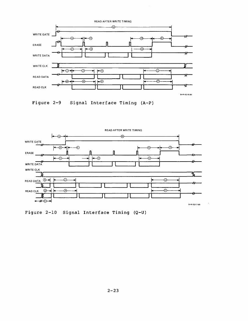
READ AFTER WRITE TIMING
~14----------~G~----------~·1 ~~------------------------------~
WRITE GATE ---11 I... -~JJ--~r---<9 ~
ERASE --11 n~ ___ ..... n~ ___ ..... n I ~1----CJf-~~ I~
JC WRITE eLK :JL~ --------------________ ..4..._
~r-<9 I" @ -I I I I Jt--READ DATA ~J I I 1'--__ .....,,11 ___ _
READ eLK ----1; I II 11 ___ ----' 14 ® ,
II I (r-1~~
SHR-0216-85
Figure 2-9 Signal Interface Timing (A-P)
READ AFTER WRITE TIMING
~H~~I·------------~®~------------~·I WRITE GATE I I
~,:r'" ---- L..-~JJ--
1---0---1~ ~ ERASE ~,...' _______ 01... ___ ....,,0"--_______ 0 .... ___ ..... 0 I '''--_-III--
t---0---i -I 1--<0 ~ ~~ ... -~--T_--~~---rl---T'----_r-----~/r--
WRITE DATA I I ~I __ ----'I ..... 1 __ ----'I I I WRITE eLK
:JSL __________________________ ~----~~SL: REA D DATA 0--l /----0---i
:JLJ , I 1 ___ --'11 '-__ --II 1 ..... _--' t @
"I I READ eLK @---.j ~ I .. ® -I
II ::JOI II II 11 __ ___ I 4---/J---0--.j
SH R-021 7-85
Figure 2-10 Signal Interface Timing (Q-U)
2-23
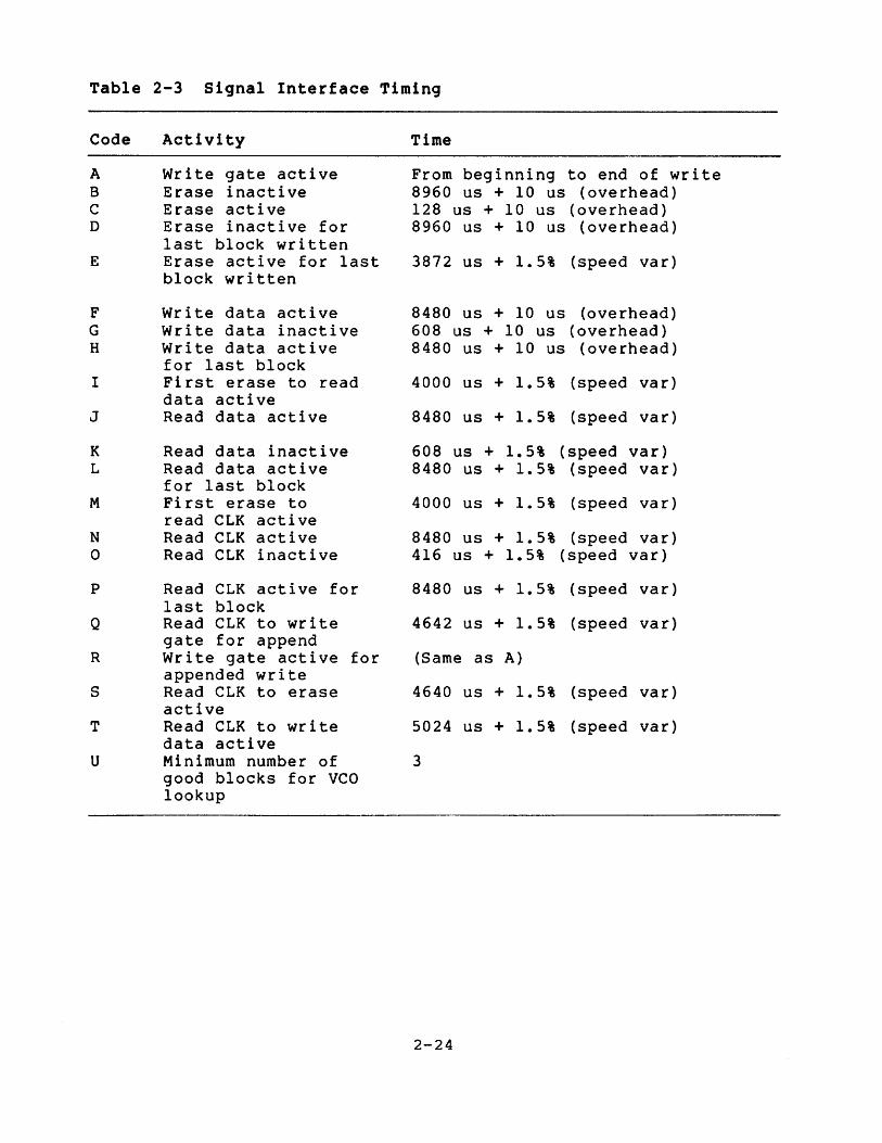
Table 2-3 Signal Interface Timing
Code
A B C D
E
F G H
I
J
K L
M
N e p
Q
R
S
T
u
Activity
Write gate active Erase inactive Erase active Erase inactive for last block written Erase active for last block written
Write data active Write data inactive Write data active for last block First erase to read data active Read data active
Read data inactive Read data active for last block First erase to read eLK active Read eLK active Read CLK inactive
Read eLK active for last block Read eLK to write gate for append Write gate active for appended write Read eLK to erase active Read CLK to write data active Minimum number of good blocks for vee lookup
Time
From beginning to end of write 8960 us + 10 us (overhead) 128 us + 10 us (overhead) 8960 us + 10 us (overhead)
3872 us + 1.5% (speed var)
8480 us + 10 us (overhead) 608 us + 10 us (overhead) 8480 us + 10 us (overhead)
4000 us + 1.5% (speed var)
8480 us + 1.5% (speed var)
608 us + 1.5% (speed var) 8480 us + 1.5% (speed var)
4000 us + 1.5% (speed var)
8480 us + 1.5% (speed var) 416 us + 1.5% (speed var)
8480 us + 1.5% (speed var)
4642 us + 1.5% (speed var)
(Same as A)
4640 us + 1.5% (speed var)
5024 us + 1.5% (speed var)
3
2-24

2.18 SERIAL CONTROLLER TO DRIVE COMMUNICATIONS
The controller sends commands to the drive through the differential signal pair DR CMD. Status is returned to the controller via the differential signal pair DR Status. The drive's 8751 microprocessor receives and interprets the commands through its built-in serial port, set up as a full-duplex UART. The drive receives drive commands via the AM26LS32 differential receiver (E13) and the microprocessor's RxD (receive data) line. Drive status is transmitted to the controller, via the AM26LS31 differential driver, from the microprocessor's TxD (transmit data) line.
The communications (UART) portion of the 8751 is programmed as follows (Figure 2-11).
Frame format 1 start, 8 data, 2 stop bits.
This is the 8751's UART Mode 2, with T88 set high to create the second stop bit.
Baud rate
Frame time
IDLE STATE
187500
59 microseconds
RETURN TO IDLE STATE OR START BIT OF
~1.-----8DATA BITS ------.j-\ NEW C,ARACTER
r------.,-- -- ---..,---,----,----,----,---..,.., --"""1'1--START: LSB : : : I I I I MSB 12 STOP BITS: I BIT, , , I , I I I I "
-------- 1=~~~:~~/~l~~E~-B~~C~::;I~~-J---L---J IL--...J -t-=58.6 U5+1-,%PER FRAMEOF 11 BITS ,-
BAUD RATE = 187.5 KHZ
Figure 2-11 Frame Format of Data Coming from Controller
2-25
SH A·0218·85
2.19 BASIC CONTROLLER/DRIVE COMMUNICATIONS PROTOCOL
This section explains the handshaking needed to transfer commands, data, and status between the drive and the controller.
2.19.1 Control1er-to-Drive Command Protocol
The drive always echoes commands back to the controller to ensure the integrity of the transmission. If data bytes other than the initial command byte are required by the command in question, they are also sent by the controller and echoed by the drive.
All commands but one must be echoed by the drive within 500 milliseconds, and all other solicited bytes must be received by the controller within one second, or it assumes that a communications error exists. The only exception is the send status command, which allows up to 9.75 seconds for the status message to be received.
2.19.2 Drive-to-Controller Status Protocol
Status sent from the drive to the controller always requires the transmission of an acknowledge message from the controller (40H), before the drive proceeds with any further communication. Two types of status messages can be transmitted from the drive to the controller: solicited and unsolicited.
Solicited status messages are those drive transmissions sent in response to a controller invoked command. Unsolicited status messages are those sent to the controller that were not requested. Drive "change of state" and "drive detected error" result in unsolicited status messages.
2.19.2.1 Change of Drive State -- A drive change of state results in the tranmission by the drive of the one-byte drive status message. Examples of this change of state message are: up to speed, rewind complete, and change of load switch state. Change of state message transmission causes an interruption of drive/controller communication until the controller acknowledges the message.
2.19.2.2 Drive Detected Errors -- An error detected by the drive results in an unsolicited "drive detected error" message to the controller. This message is always preceded by an error notification (80 hex) to the controller. After the controller acknowledges the error notification message, one of the error codes defined in Section 4.2 is transmitted to the controller. The transmit/acknowledge protocol is used throughout the error message interchange between the drive and the controller.
2-26

2.20 TK50 COMMANDS
Table 2-4 lists and defines the commands that the controller provides to the drive via the 26-pin flat ribbon cable. These serial commands are received and decoded by the 8751 microprocessor at El on the drive logic module. The 8751 controls the remainder of the circuits in the drive logic, to perform the operations necessary to successfully execute the command.
Table 2-4 TK50 Commands
Command
RESET SNDREV SDSTAT CLRERR SDREGO
SDREGC SDBKAD LDBKAD SNDERR SDDOCT
SKTRKX STDAGC LOAD MEDIA B5CMD
CALEDG CALIBR REWIND UNLOAD LOAD
MOVFWD MOVBWD SEEK BSPACE FSPACE
DOS TOP BSTOP STOP HEADI HEAD2
Code
00 01 02 03 04
05 06 07 08 09
OA OB OC OD OE
OF 10 11 12 13
14 15 16 17 18
19 lA IB Ie ID
Definition
Reset MPU and drive Send software/hardware revision level Send Drive Status Byte (DRSTAT) Clear Drive Error Bytes Send register contents
Continue sending register contents Send tape count Load tape count Send the two error bytes Send dropout data
Step head to track X Set read gain to standard value Load tape command (Diagnostic) Diagnostic test for media dropout Diagnostic automatic exercise
Calibrate to tape edge only Calibrate track position Rewind to BOT Software unload tape Move forward at load speed
Move forward (TRKADR) Move backward (TRKADR) Seek to block Backspace for R/W forward Space forward for R/W backward
Media test, stop on dropout Space opposite, before stop Stop tape Select head 0 Select head 1
2-27

Table 2-4 TK50 Commands (Cont)
Command
ENWRT CLRWRT SMPDRP ENVCO ENREAD
DISCRP SMPCIR TRK-1 TRK+1 ONESTP
Code
IE IF 20 21 22
23 24 25 26 27
Definition
Enable write Clear write and erase mode Sample dropout data, in "WM" Software enable VCO Software enable read (Diagnostic)
Disable sampling dropouts Sample motor current, tape speed -1 mil offset during present move +1 mil offset during present move 1 mil step command
TK50 commands can be grouped into four basic types: Control, Motion, On-the-Fly, and Diagnostic commands.
2.21 TK50 DRIVE STATES
There are two classes of drive states: Drive Normal Status and Drive Error Status. Changes in drive state into either one of these classes cause an unsolicited status message to be sent to the controller (see Section 2.19.2 Drive to Controller Protocol). The controller processes and acts on state change messages as detailed in this section.
2.21.1 Drive State Status
Drive state changes that do not indicate a drive detected error result in the drive sending a hexadecimal code to the controller indicating the current drive state (or state changed to). The controller responds to this type of state change transmission with an acknowledge. Table 2-5 lists the nonerror drive states and the following subsections explain them.
Table 2-5 Nonerror Drive States
Code Status
40 50 60 70 NA
Done Enable write gate Dropout sensed Track boundary Load/run state change (see Paragraph 2.21.1.5)
2-28

2.21.1.1 Done (40) The Done state has multiple meanings, depending on the drive/controller events occuring before the Done message is transmitted. This state usually signifies that the drive has completed a controller-invoked event, such as up to speed, BOT sensed, or tape motion stopped.
2.21.1.2 Enable Write Gate (50) -- The enable write gate state is used during the head calibration sequence. It requests the controller to assert the Enable Write Gate signal.
2.21.1.3 Dropout Sensed (60) Dropout Sensed status is transmitted for every dropout detected by the drive when in the dropout test diagnostic mode.
2.21.1.4 Track Boundary (70) -- The Track Boundary state signals to the controller that the beginning or end of a logical track was encountered during normal tape motion.
2.21.1.5 Load/Run State Change (Table 2-6) -- Load/Run State Change is sent to the controller when the drive senses that its front panel load switch is changed from run to unload. Drive initiation of the unload operation won't begin until the controller issues a Stop or Reset command.
Table 2-6 Send Status Byte Bit Assignments
Bits 7 6 5 4 3 2 1 0
0 0 0 0 0 0 0 0 Request for initialization 0 0 X X X X X 1 Cartridge is present 0 0 X X X X 1 X Head is positioned on Track 0 0 0 X X X 1 X X Unload state 0 0 X X 1 X X X Write Lock state 0 0 X 1 X 0 X 1 BOT state 0 0 1 X X 0 X 1 Run state 0 0 1 1 X 0 X 1 Rewind in progress 1 0 0 0 0 0 0 0 Error state
X = Don't care
2-29
2.21.2 Drive Error Status
When a drive detected error occurs, it causes the drive to send an unsolicited error message (BOH) to the controller. The controller acknowledges the error indication with a normal acknowledge message (40H). When the drive receives and decodes the 40H, it sends the error code that corresponds to the drive detected error.
Drive error status messages all have bit 7 of their corresponding hexadecimal code set. All drive error status codes that are less than 90H are fatal drive errors and cause the termination of drive/controller communication. All nonfatal drive errors have a hexadecimal code of 90H or. greater, and allow resumption of drive/controller communication after the controller issues a Clear Drive Error command.
2-30

3.1 INTRODUCTION
CHAPTER 3 OPERATING
PROCEDURES
The TK50 is a relatively new type of device. It's use may not be immediately obvious. Read this chapter completely first, then perform the procedures in Sections 3.4 and 3.5. The TK50 Tape Drive Subsystem User Reference Card, EK-OTK50-RC, can be used as a reminder after you become comfortable using the drive.
The TK50 uses a tape cartridge (labeled CompacTape) that contains the magnetic tape on a single reel. This is an important concept to understand, because it directly affects the use of the TK50. The magnetic tape is the medium that stores the data.
When the tape cartridge is loaded into the drive, the tape is automatically threaded onto a reel inside the drive. If the tape is fully wound onto the reel inside the drive, it can take up to 90 seconds to rewind. It must be fully rewound into the cartridge before the cartridge can be removed.
This method is different from a video cassette recorder (VCR) in that a VCR tape can be ejected at any time -- it does not have to be rewound first.
3-1
3.2 ABOUT THE TAPE CARTRIDGE The TKSO tape cartridge is a 4-inch by 4-inch plastic cartridge that is inserted into the TKSO tape drive. It is labeled CompacTape.
The tape cartridge has a write-protect switch to prevent accidental erasure of important data. When the switch is moved to the left and the orange indicator is visible, data cannot be written to the tape.
Inside the cartridge is a 600-foot single reel of magnetic tape, on which data is stored. At the beginning of the tape is a plastic leader. There are some rules to follow about the tape cartridge.
•
•
• 3.3
Do not drop the cartridge. This may cause the leader to be displaced, in which case the tape cartridge is unusable, and it may damage the drive. (See Section 3.4, Inspecting and Loading a Tape Cartridge.)
If the tape cartridge has been exposed to extremes of heat or cold, let it stabilize at room temperature for the same amount of time -- up to 24 hours.
Do not touch any exposed portion of magnetic tape.
TERMS USED IN THIS CHAPTER
Cartridge leader A plastic leader at the beginning of the magnetic tape. Consider that the mating of the leaders (one of which is inside the cartridge, the other inside the drive) is like the threading of a needle. The leader inside the cartridge serves
Take-up leader
as the "eye" of the needle. This leader may be either black or white.
A plastic leader inside the TK50. After the take-up leader mates with the cartridge leader, it draws the magnetic tape out of the cartridge and onto the take-up reel inside the tape drive. As the tape is wound onto the take-up reel, it passes the magnetic read and write heads. These heads let the TK50 perform its function: to write and read data to and from the magnetic tape.
3-2
Cartridge insert/
Insertion
Load
Unload
BOT
write protect
This handle is used to set the internal release handle mechanisms of the TKSO to accept or eject the tape cartridge. The handle is raised before inserting a cartridge, lowered during use, and raised again to eject the cartridge.
The act of placing the tape cartridge in the TK50. It is during insertion that the cartridge leader and take-up leader mate. Before insertion it is important (especially the first time the cartridge or drive is used) to inspect the positions of both the cartridge leader and take-up leader. Refer to Section 3.4 for instructions.
When the tape cartridge has been correctly inserted, the tape is brought to BOT by pushing the Load/Unload switch and releasing it to its In, or Load, position.
After you finish using the tape cartridge, push and release the Load/Unload switch to its Out position. The tape rewinds to BOT, then to its unload point. Now you can lift the handle and remove the cartridge from the tape drive.
Beginning of Tape. It is the first spot on the magnetic tape where data can be written. BOT is set automatically. You need perform no functions in regard to BOT.
A switch on the TK50 tape cartridge used to prevent data from being written on the tape. In its protected position, a small orange indicator is visible on the front of the tape cartridge. In its enabled position, there is no orange dot visible and data may be written to the cartridge.
3-3

3.4 INSPECTING AND LOADING A TAPE CARTRIDGE
This section is a 10-step procedure that explains how to inspect and label a tape cartridge, turn on power, and load the cartridge into the TK50 Tape Drive.
1. Inspect the tape cartridge.
Always inspect the tape cartridge before you use it for the first time. Open the cartridge door by releasing the door lock with your thumb. The tape leader inside the cartridge should be positioned exactly like the one shown in Figure 3-1. The cartridge leader may be either black or white.
/
CAUTION If the leader is not positioned exactly as that in Figure 3-1, do not use this cartridge. It may damage the drive. Do not pull the leader. Do not drop the tape cartridge.
DOOR LOCK (RELEASE BY LIFTING DOOR LOCK WITH THUMB)
LEADER EYE CARTRIDGE LEADER
CARTRIDGE LEADER IN FULL VIEW
SHR OD01 86
SHA-0002-S6
Figure 3-1 Inspecting Tape Cartridge
3-4

2. Label the tape cartridge (Figure 3-2).
Always label the tape cartridge you're using, so that later you'll know what information is on the tape.
There is a slot on the front of the tape cartridge for a slide-in label.
Use only label a stick-on sides of
CAUTION the label slot provided to
tape cartridge. Do not use labels on the top, bottom, or
the tape cartridge.
SH R-0298-84 A
Figure 3-2 Labeling Tape Cartridge
3-5
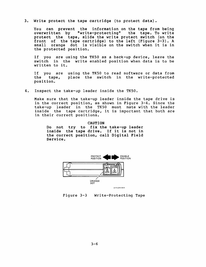
3. Write protect the tape cartridge (to protect data).
You can prevent the information on the tape from being overwritten by "write-protecting" the tape. To write protect the tape, slide the write protect switch (on the front of the tape cartridge) to the left (Figure 3-3). A small orange dot is visible on the switch when it is in the protected position.
If you are using the TK50 as a back-up device, leave the switch in the write enabled position when data is to be written to it.
If you are the tape, position.
using the TK50 to read software or data from place the switch in the write-protected
4. Inspect the take-up leader inside the TK50.
Make sure that the take-up leader inside the tape drive is in the correct position, as shown in Figure 3-4. Since the take-up leader in the TK50 must mate with the leader inside the tape cartridge, it is important that both are in their correct positions.
CAUTION Do not try to fix the take-up leader inside the tape drive. If it is not in the correct position, call Digital Field Service.
Figure 3-3
PROTECT •• ENABLE POSITION POSITION
ORANGE DOT
SHR029984A
Write-Protecting Tape
3-6

BUCKLING LINK
~/_-~[Q] CARTRIDGE INSERT/RELEASE HANDLE DOWN
Figure 3-4 Inspecting Leader
3-7
SHR·0003·86
} ACCEPTABLE
UNACCEPTAB LE CALL FIELD SERVICE
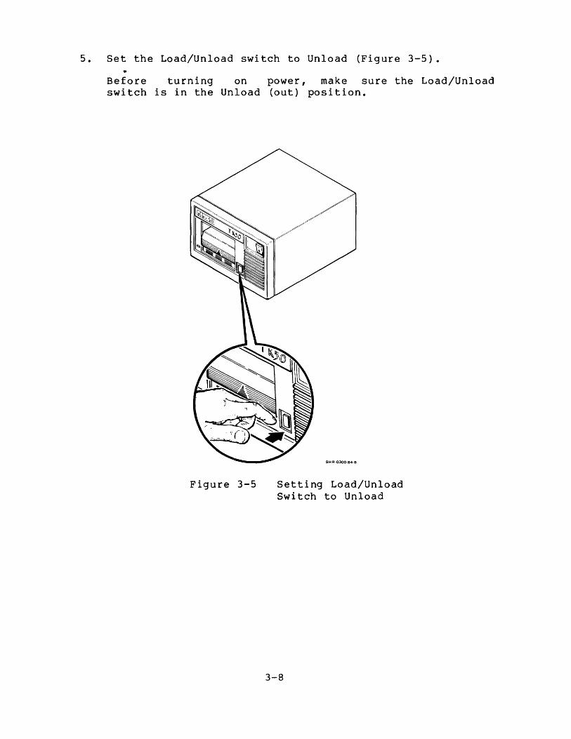
5. Set the Load/Unload switch to Unload (Figure 3-5).
Before turning on power, make sure the Load/Unload switch is in the Unload (out) position.
Figure 3-5 Setting Load/Unload Switch to Unload
3-8

6. Watch the lights and turn on the power (Figure 3-6).
Turn on the power to the TK50. The tape drive's red light goes on steady for about 5 to 15 seconds (while it runs an internal self-test), then goes off. The green light comes on. If at any time the red light flashes rapidly, there is a problem with the TK50.
SH R-0301-84-B
Figure 3-6 Turning on Power
3-9

7. When the green light goes on (the red light is off), lift the cartridge insert/release handle (Figure 3-7).
If you have a TK50 that is mounted vertically in a floor stand computer system, "lifting" the cartridge insert/release handle means pulling it to the left.
CAUTION Never lift the cartridge insert/release handle when the red light is on or blinking or you may cause a fault or damage the unit.
Before performing step 8, read the Caution.
8. Smoothly and completely insert the tape cartridge.
Hold the tape cartridge with the arrow on top, pointing away from you. Make sure the label is facing you. Place the cartridge partially into the drive as shown in the first part of Figure 3-8. Push the cartridge (as shown in the second part of Figure 3-8) into the drive, smoothly and firmly, until it locks in place inside the drive. Now the red light comes on and the green light goes off.
CAUTION You will feel some resistance as you push the cartridge into place. It 1S very important NOT TO STOP AT THIS POINT, BUT TO CONTINUE TO PUSH THE CARTRIDGE FIRMLY UNTIL IT LOCKS IN PLACE.
Figure 3-7 Lifting Cartridge Insert/Release Handle
3-10
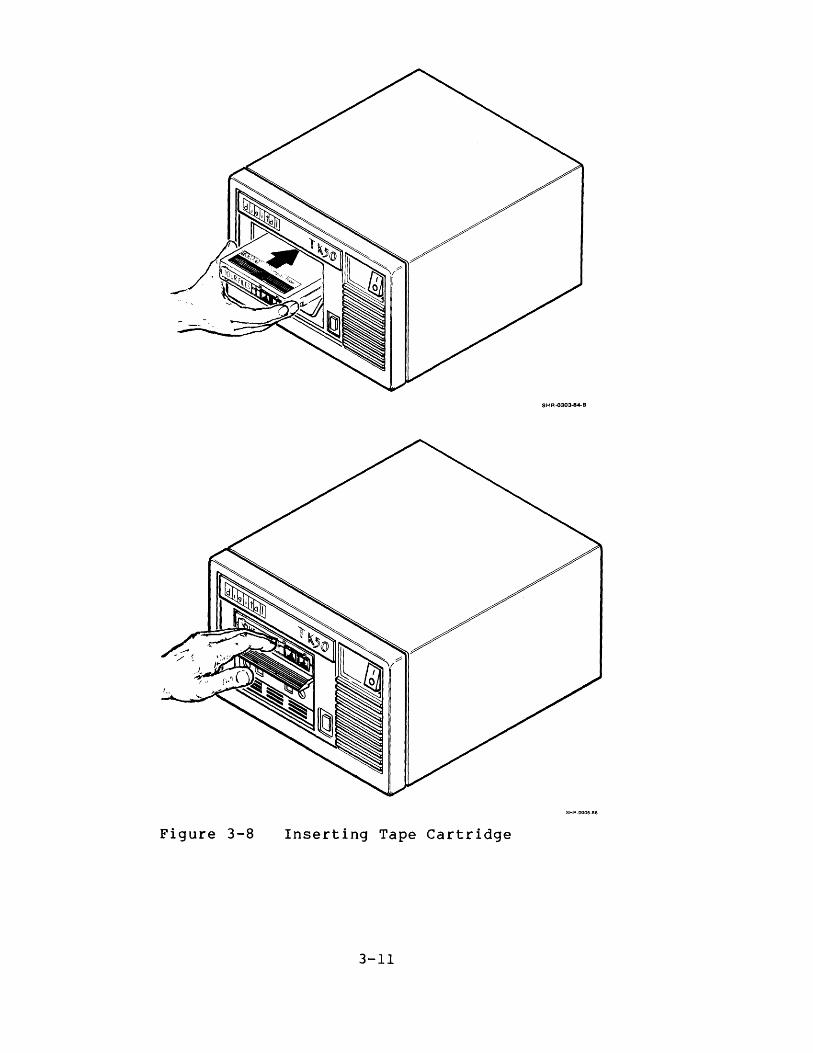
SHR.(I303·84-8
Figure 3-8 Inserting Tape Cartridge
3-11

9. Lower the cartridge insert/release handle to locked (closed) position (Figure 3-9).
After a delay of several seconds, the green light comes on steady, the red light goes off.
At this point, you can remove the tape cartridge by lifting the handle, or go on to the next step.
Figure 3-9 Lowering Cartridge Insert/Release Handle
3-12

10. Set the Load/Unload switch to load (In position).
Push in the Load/Unload switch (Figure 3-10). The tape goes through a load process that takes between 5 and 7 . seconds. Both lights come on steady as the tape reaches BOT (the beginning of usable tape).
The tape cartridge is now ready to use.
SH R·0305·84·C
Figure 3-10 Setting Load/Unload Switch to Load
3-13
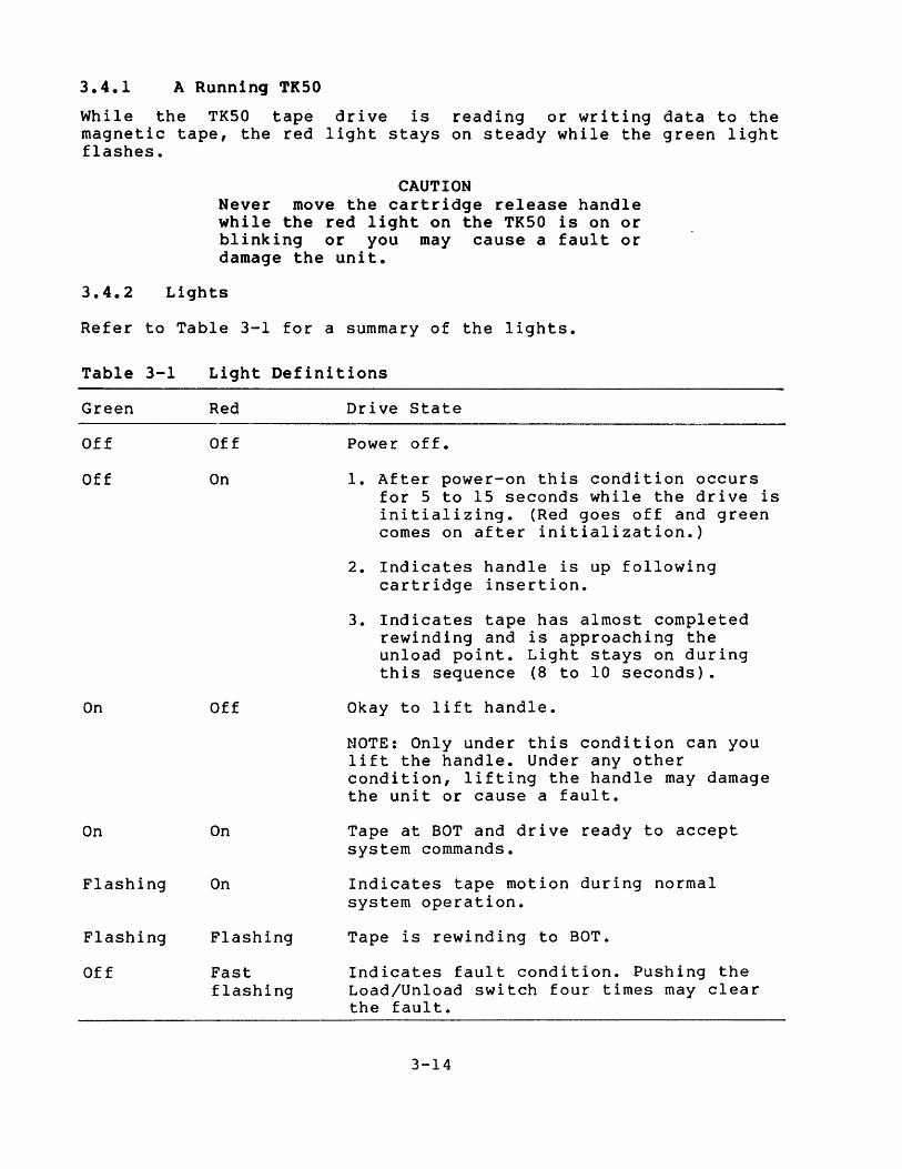
3.4.1 A Running TKSO
While the TKSO tape drive is reading or writing data to the magnetic tape, the red light stays on steady while the green light flashes.
CAUTION Never move the cartridge release handle while the red light on the TKSO is on or blinking or you may cause a fault or damage the unit.
3.4.2 Lights
Refer to Table 3-1 for a summary of the lights.
Table 3-1
Green
Off
Off
On
On
Flashing
Flashing
Off
Light Definitions
Red
Off
On
Off
On
On
Flashing
Fast flashing
Drive State
Power off.
1. After power-on this condition occurs for 5 to 15 seconds while the drive is initializing. (Red goes off and green comes on after initialization.)
2. Indicates handle is up following cartridge insertion.
3. Indicates tape has almost completed rewinding and is approaching the unload point. Light stays on during this sequence (8 to 10 seconds).
Okay to lift handle.
NOTE: Only under this condition can you lift the handle. Under any other condition, lifting the handle may damage the unit or cause a fault.
Tape at BOT and drive ready to accept system commands.
Indicates tape motion during normal system operation.
Tape is rewinding to BOT.
Indicates fault condition. Pushing the Load/Unload switch four times may clear the fault.
3-14

3.5 UNLOADING THE TAPE
This section explains how to remove the tape cartridge from the drive.
1. Set the Load/Unload switch to Unload (Out position) (Figure 3-11).
If the tape is not already at BOT, both lights flash slowly while the tape is rewinding.
If very little tape was in the drive when you set the Unload switch, you may not see the lights flash when the tape is rewinding. Whether or not you see the flash depends on how much of the tape was out on the take-up reel inside the drive.
The red light comes on steady while the tape is unloading. The unload process takes between 8 and 10 seconds to complete. After the tape unloads, the red light goes off and the green light comes on. It is now safe to remove the tape cartridge.
SH R-0305-84-D
Figure 3-11 Setting Load/Unload Switch to Unload (to Rewind)
3-15

2. After the red light goes off and the green light comes on, lift the cartridge insert/release handle (Figure 3-12). If you have a system-integrated TKSO mounted vertically in a floor stand computer, "lifting" the handle means pulling it to the left.
The tape partially ejects.
CAUTION Never lift the cartridge release handle while the red light is on or blinking or you may cause a fault or damage the unit.
SHA-0307-B4-B
Figure 3-12 Ejecting Tape Cartridge (After Rewind)
3-16

3. Remove the cartridge and return it to its protective case (Figure 3-13).
CAUTION Remove the tape cartridge from the drive before turning power off. Damage may occur if the tape drive is moved with a cartridge inserted and power is off.
SH R-0308-B4-B
Figure 3-13 Removing Tape Cartridge
3-17

4. Turn the power switch off (0 position) (Figure 3-14). Push the cartridge insert/release handle down.
Whenever you turn the power off in a tabletop unit, you'll hear some whistling and whirring noises. Don't worry, this is normal.
Figure 3-14 Turning Off Power
3-18
3.6 TKSO APPLICATIONS
This section describes ways you can use the TKSO Tape Drive Subsystem.
3.6.1 As a Back-Up Device
You can use the TKSO as a back-up device by copying files from another device (usually a fixed disk drive such as an RD51 or RD52), onto the TK50's cartridge. The TK50's large storage capacity makes it much easier to use for large backup operations than floppy disks, because it can store much more information.
To back up a file onto the TK50, you must run a "utility program" under your operating system that copies data from one device to another. Most operating systems have a variety of utility programs that can transfer files between devices. Refer to your operating system user manual for instructions on how to perform a back up or file copy operation.
3.6.2 As a Software Distribution Medium
The TK50 is ideal as a software distribution medium because an entire operating system can be stored on one cartridge. Rather than using many floppy disks to load an operating system onto your computer, you can use one TK50 cartridge. When used this way, the TKSO is almost exclusively a "read-only" device, which means that you won't be writing data to the cartridge. If you are using the TK50 to load software on your system, make sure that the tape cartridge is write protected.
3.6.3 As a -Journaling- Device
Due to its large storage capacity, the TK50 is ideal for systems where large amounts of data are sequentially written to a peripheral device. An example of this is a system used for monitoring a process over a long period of time. The data gathered can be sequentially written to the TK50 cartridge, then, at a convenient time, the cartridge can be removed and the data read back onto another system for analysis.
3-19

CHAPTER 4 DRIVE UNIT REPAIR
4.1 GENERAL
This chapter provides information on diagnosing and repairing the drive unit of the TK50 Tape Drive Subsystem. The chapter is divided into two major sections: first, it lists the error codes that the subsystem microcode generates when an error is detected; second, it provides instructions on how to remove a failed subassembly.
This chapter is not intended to be used for field troubleshooting. Since the drive unit is a Field Replaceable Unit (FRU) , the field engineer will not be troubleshooting it to the subassembly level, but replacing it as a whole. This chapter is for technicians at Field Repair Depots.
4.2 Error Codes
This section provides error codes, lists probable causes for the error, and recommends actions to be taken to repair the drive. Section 4.3 gives instructions for removing and replacing subassemblies that failed. The error codes listed are those reported to the operating system error log.
4.2.1 Failure to Load to Beginning of Tape (BOT) -- (81H)
Causes:
1. Supply/takeup leader length is incorrect (if second error byte = 96H = BOTER).
2. There is an obstruction in tape path (if second error byte = 87H = DRAGER).
3. BOT sensor is marginal.
4-1

Recommended Action:
1. Replace cartridge and retest.
2. Check for and fix causes of drag, if possible.
3. Inspect BOT/EaT sensor and wiring. Replace BOT/EDT sensor if necessary.
4.2.2 Failure to Load Tape into Cartridge (82H)
Causes:
1. Supply/takeup leader length is incorrect; second error byte = 096H (BaTER).
2. There is an obstruction in tape path; second error byte = 87H (DRAGER).
3. Motor A (supply motor) rotated in wrong direction; second error byte = 8FH.
Recommended Action:
1. Replace cartridge, retest.
2. Check for and fix causes of drag, if possible.
3. Inspect BOT/EDT sensor and wiring. Replace BOT sensor if necessary.
4.2.3 General Motor or Tachometer Failure (83H) -- A hard pull on Motor B produces less than 5 tach pulses with BOT off.
Causes:
1. Motor B stalled or is not connected.
2. Tachometer is bad or not connected (produces no pulses).
3. Leader is stuck in tape path.
4. Cartridge jammed.
4-2
Recommended Action:
1. Check all cable connections.
2. Check for and remove friction in tape path.
3. Replace Motor B or tachometer.
4.2.4 Motor A Failure (Supply Motor) -- (848)
Motor A was pulling against motor B without sensing a reversal of direction via the motor A Hall switches.
Causes:
1. Supply motor is bad or not connected.
Recommended Action:
1. Replace Motor A (supply motor) •
4.2.5 Motor B Failure (Take-up Motor) -- (858)
Motor B was pulling with excessive current and motor A did not rotate a minimum of 90 degrees. Tachometer pulses were present.
Causes:
1. Motor B is bad or there was an obstruction in the tape path.
2. Motor A Hall switches are not functioning or not properly received.
Recommended Action:
1. Check for obstruction in tape path and cabling problem.
2. Check whether both Hall switches at MPU are toggling when Motor A rotates.
3. Replace faulty motor (A or B).
4-3

4.2.6 Drive Lost Control of Tape or Bad Tachometer -- (86B)
The drive experienced either incorrect spacing of tach pulses or an insufficient number of pulses were detected.
Causes:
1. Motor A or Motor B is bad.
2. Tach problem, high friction on the tape, or the tape stalled.
3. There is no tape in path.
Recommended Action:
1. Check for tape presence.
2. Check for drag in tape path.
3. Check motors.
4. If no trouble is found, reset drive and get detail error report (if any) via initialization procedure.
4.2.7 Excessive Drag in Tape Transport -- (87B)
Currents to the motors exceeded limits in servo mode.
Causes:
1. There is a jam or interference in tape path.
2. Tape overran EOT marker, now is at tape end.
3. One of the motors is bad.
Recommended Action:
1. Check for obstruction in tape path.
2. Reset drive and observe any error messages during drive initialization (repeat several times).
4-4

4.2.8 Failure to Stop Tape or Remain Stopped -- (88H)
Excessive tach pulses during deceleration mode.
Causes:
1. Motors are out of spec.
2. One of the motors is bad.
3. Bad tape reel estimate during initialization.
Recommended Action:
1.
2.
4.2.9
Reset drive several times and observe stop at low speed and after rewind.
Replace faulty motor(s).
'Cartridge Insert Error -- (89H)
The drive experienced improper timing or occurrences of the unload/BOT signal or tachometer signal.
Causes:
1. Leaders are misaligned.
2. EOT/BOT circuit is bad.
3. There is high drag in tape path.
4. Handle switch is bad.
NOTE Specific error in second error byte.
Recommended Action:
1. Check for and remove obstruction in tape path.
2. Check and repair leader alignment.
3. Check and/or replace cartridge.
4. Check and/or replace leader mechanism.
4-5

4.2.10 Cartridge Extract Error -- (SAH)
BOT sense was lost or there were insufficient tachometer pulses in 25 seconds.
Causes:
1. Leaders are misaligned.
2. BOT/EOT circuit is bad.
3. Cartridge only partially ejected.
4. There are too many tach pulses. Drive leader did not engage.
Recommended Action:
1. Check for interference in receiver.
2. Check eject mechanism and springs.
3. Replace drive leader if damaged.
4.2.11 Move Error (8BH)
The controller tried to move the tape while the drive was in an error state, or the drive was still in an error state when the controller issued a tape motion command.
Causes:
1. Block address overflow or underflow is not received by the controller.
2. A new command and error message occurred at the same time.
3. Controller is out of sequence.
4. Operator interfered.
Recommended Action:
1. Restart.
4-6
4.2.12 Deceleration Error -- (SCH)
The servo exceeded the time allotted to slow down to S.5 inches per second.
Causes:
1. Motor A is bad, or motors are out of spec.
Recommended Action:
1. Reset drive and observe detail error messages, if any.
2. Replace Motor A.
4.2.13 Reel Error -- (8DH)
A second. attempt Improper balance supply reel.
Causes:
to or
balance the distribution
reels of tape
in the unit failed. between take up and
1. Tape overran logical EDT and is now at tape end.
2. Tape is too short between EOT hole and end.
3. Tachometer and/or Motor A Hall switch connection is intermittent.
Recommended Action:
1. Rewind tape 20 turns minimum into cartridge if at tape end.
2. Power up.
3. Replace cartridge.
4.2.14 Check Byte Error -- (SEH)
Causes:
1. 8751 microprocessor is bad.
Recommended Action:
1. Replace drive board.
2. Replace microprocessor.
4-7

4.2.15 Unload Error -- (8FH)
The unload microdiagnostic test failed.
Causes:
1. Motor A went in the wrong direction. The motor is bad.
Recommended Action:
1. Replace Motor A.
4.2.16 8155 Memory Error -- (90H)
The 8155
memory microdiagnostic test failed during initialization. RAM locations were loaded with an address, then read back
wrong.
Causes:
1. The 8155 is bad.
2. The 8751 microprocessor has a bad bus.
Recommended Action:
1. Inspect drive board for broken leads, etches.
2. Re-seat socketed 8751 microprocessor, retest.
3. Replace drive board.
4.2.17 8155 Timer Error -- (91H)
A timer in the 8155 failed. The 8155 timers were tested against the 8751's timers and were incorrect or not operational.
Causes:
1. The 8155 is bad.
2. The 8751 has a bad I/O bus.
Recommended Action:
1. Re-seat 8751 microprocessor and retest.
2. Replace the 8155 or the drive board.
4-8

4.2.18 Read Head 1 Error -- (92H)
The read amplitude on head 1 was too low during calibration. The signal during calibration was insufficient.
Causes:
1. Calibration tracks on the tape are bad.
2. Read head cables are bad or intermittent.
3. Head is contaminated.
Recommended Action:
1. Inspect the head and cables. Is there continuity?
2. Wipe the head with a dry tissue (not on customer site).
3. Replace the head.
4.2.19 Read Head 2 Error -- (93H)
The read amplitude on head 2 was too low during calibration. The signal during calibration was insufficient.
Causes:
1. Calibration tracks on the tape are bad.
2. Read head cables are bad or intermittent.
3. Head is contaminated.
Recommended Action:
1. Inspect the head and cables. Is there continuity?
2. Wipe the head with a dry tissue (not on customer site).
3. Replace the head.
4-9
4.2.20 Cartridge Insert/Extract Error -- (94H)
A runaway condition during the insertion or extraction of the tape cartridge.
Causes:
1. Handle microswitch is bad or not connected.
Recommended Action:
1. Check handle microswitch connector.
2. Replace handle microswitch connector.
4.2.21 EOT Sensed in Read/Write/Seek State -- (95H)
The drive failed to handle the logical end of tape marker and reached physical end of tape.
Causes:
1. Communication between the drive and the controller is faulty. The controller lost power while the tape was moving.
2. There is a drive/controller communications protocol problem.
3. Tachometer is intermittent.
4. Tape is too short.
5. There are hole(s) in the tape.
6. BOT/EOT circuit failed.
Recommended Actions:
1. Inspect tachometer connections.
2. Reset.
3. Restart, retest.
4. Replace the drive board.
4-10

4.2.22 BOT Sensed in Read/Write/Seek State -- (968)
The drive failed to handle the logical beginning of tape marker and encountered physical beginning of tape.
Causes:
1. Communication between the drive and the controller is faulty. The controller lost power while the tape was moving.
2. There is a drive/controller communications protocol problem.
3. Tachometer is intermittent.
4. Tape is too short.
5. There are hole (s) in the tape.
6. BOT/EDT circuit failed.
7. Bad reel size estimate during initialization.
Recommended Actions:
1. Inspect tachometer connections.
2. Reset.
3. Restart, retest.
4. Replace the drive board.
4.2.23 Address Overflow Error -- (97H)
A drive block address overflow occurred and exceeded the usable area on the tape.
Causes:
1. The controller failed to issue a stop command or lost power.
Recommended Action:
1. Clear error and rewind.
2. Reset, restart.
3. Troubleshoot loss of power; replace controller.
4-11

4.2.24 Address Underflow Error -- (98H)
A drive block address underflow occurred and exceeded the usable area on the tape.
Causes:
1. The controller lost power while tape was moving backward.
Recommended Action:
1. Clear error and rewind.
2. Reset, restart.
3. Troubleshoot loss of power; replace controller.
4.2.25 Servo Error -- (99H)
Excessive speed variations, exceeding limits, wobble (balance problem in tape reels).
Causes:
1. There is a problem with the cartridge, bearing, and spring load.
2. There is a problem with the radial/vertical runout of hubs.
3. There is a problem with the runout/balance of capstans.
4. Tach connection is intermittent, extra pulses.
5. One motor is bad.
Recommended Action:
1. Inspect for excessive runout.
2. Inspect tachometer connection.
3. Reset drive. Observe detail error messages, if any.
4.2.26 Failure in Tracking -- (9AH)
Reserved for future use.
4-12

4.2.27 Command Error (9BH)
The command from the controller was not recognized.
Causes:
1. Interface cabling is faulty.
2. There is a bad receiver chip on the drive module, or bad driver chip on the controller module.
Recommended Action:
1. Reinsert or replace cable.
2. Replace module(s).
4.2.28 Illegal Command -- (9CH)
The command issued was incompatible with the drive state.
Causes:
1. There is a communication/protocol error with controller.
2. Operator forced an unload while the controller started to read, write, or seek.
Recommended Action:
1. Restart and observe sequence.
2. Potential hardware/software problem.
4.2.29 Write Lock Error -- (9DH)
The tape was in a write-locked state when a write operation was requested.
Causes:
1. Cartridge write protect tab was in wrong position.
2. Write protect switch on the cartridge is faulty or misaligned.
3. There is a bad cable connection or broken wire.
4. There is a bad cartridge (broken plastic pin).
4-13

Recommended Action:
1. Check the write protect switch on the cartridge.
2. Check the cable.
3. Replace the cartridge.
4.2.30 Write Gate Signal Timing Error -- (9EH)
The write gate signal from the controller was received when the tape was stopped.
Causes:
1. There is a problem with the controller timing/logic.
2. Drive to controller cable.
3. Bad receiver chip on the drive board.
4. Bad driver chip on the controller.
Recommended Action:
1. Restart, retest.
2. Replace module(s) controller, then drive.
3. Replace the cable.
4.2.31 No Write Gate Error -- (9FH)
Write gate was not asserted after the request during calibration.
Causes:
1. There is a problem with the controller timing/logic.
2. There is a problem with the drive/controller cable.
3. Receiver (drive) or driver (controller) is bad.
4. Pin connection on microprocessor is bad.
Recommended Action:
1. Reinsert the cables.
2. Reinsert the 8751 microprocessor.
3. Restart.
4-14

4. Replace module(s).
4.2.32 Error Sensing CALTRACKl -- (AOH)
Causes:
1. Media has degraded.
2. There is a problem with head cables, connector.
3. Head is failing.
4. Head is contaminated.
5. Tape is partially erased or overwritten.
Recommended Action:
1. Replace cartridge.
2. Inspect head cables and connectors.
3. Wipe the head with a clean dry tissue (not on customer site) •
4. Replace the head.
4.2.33 Error Sensing CALTRACK2 -- (AlH)
Causes:
1. Media has degraded.
2. There is a problem with head cables, connector.
3. Head is failing.
4. Head is contaminated.
5. Tape is partially erased or overwritten.
Recommended Action:
1. Replace cartridge.
2. Inspect head cables and connectors.
3. Wipe the head with a clean dry tissue (not on customer site) •
4. Replace the head.
4-15

4.2.34 CALTRACK 1 Error - (A2H)
Edge detection of CALTRACKI was out of specification.
Causes:
1. Media has degraded.
2. There is a problem with head cables, connector.
3. Head is failing.
4. Head is contaminated.
5. Tape is partially erased or overwritten.
Recommended Action:
1. Replace cartridge.
2. Inspect head cables and connectors.
3. Wipe the head with a clean dry tissue (not on customer site) •
4. R&place the head.
4.2.35 CALTRACK2 Error -- (A3H)
Edge detection of CALTRACK2 was out of specification.
Causes:
1. Media has degraded.
2. There is a problem with head cables, connector.
3. Head is failing.
4. Head is contaminated.
5. Tape is partially erased or overwritten.
Recommended Action:
1. Replace cartridge.
2. Inspect head cables and connectors.
3. Wipe the head with a clean dry tissue (not on customer site) •
4. Replace the head.
4-16

4.2.36 CALTRACK2 Offset Error -- (A4H)
The offset of CALTRACK2 from CALTRACKI is too great. The distance and number of steps needed to move from CALTRACKI to CALTRACK2 is too great.
Causes:
1. Tape is partially erased.
2. The read/write head is bad.
3. Stepper motor is bad.
Recommended Action:
1. Replace cartridge.
2. Wipe head with clean dry tissue (not on customer si te) •
3. Inspect head cables and connectors.
4. Replace the head.
5. Replace the stepper motor.
4.2.37 Tape Edge Error -- (ASH)
A search for the top edge of the tape failed.
Causes:
1. Stepper motor is bad.
2. Top head is not writing or reading.
3. There is excessive feed through.
4. Drive board is bad.
5. Head is contaminated.
Recommended Action:
1. Inspect cables and shield.
2. Wipe the head with a clean, dry tissue (not on customer site) •
3. Replace the read/write head.
4. Replace the drive board.
4-17

4.2.38 Top Tape Edge Tolerance Error -- (A6H)
Causes:
1. Stepper motor is bad.
2. There is a problem with the cabling to stepper motor.
Recommended Action:
1. Check the mounting of the stepper motor and the cabling to it.
2. Operate the stepper motor in self-test mode if not cycling.
3. Replace the stepper motor.
4.2.39 Drive is Overheating -- (A7H)
Causes:
1. Airflow is blocked.
2. System fans are inoperative.
3. Thermal sensor is bad.
Recommended Action:
1. Remove air flow blockage.
2. Troubleshoot system fan problem.
4.2.40 BOT Sensor Error -- (A8H)
There is no current in the BOT/EaT sensor/assembly.
Causes:
1. Cable is unplugged.
2. BOT/EaT sensor is faulty.
3. LED driver/sense circuit is bad.
Recommended Action:
1. Check cable, replace if necessary.
2. Replace the BOT/EaT Sensor.
4-18

3. Replace the drive board.
4.2.41 No Hall Switch Signals -- (A9H)
The microprocessor on the drive board does not receive hall switch signals from motor A.
Causes:
1. There is a problem with the cable connection between motor A (supply) and the 8751 microprocessor.
2. Motor A is bad.
Recommended Action:
1. Inspect and/or repair cable connections if necessary.
2. Reseat the 8751 microprocessor in its socket.
3. Replace the supply reel motor.
4.2.42 No Tachometer Pulses Present -- (AAH)
The tachometer does not produce tachometer pulses while the tape is moving, as sensed by the motor A hall switches.
Causes:
1. The cable connection is bad, plugged in incorrectly.
2. Tachometer is bad.
3. Comparator in drive board is bad.
4. Pulley seized on bearings.
Recommended Action:
1. Inspect the cabling. Check to be sure that plugs are in the right place.
2. Reseat the 8751 microprocessor in its socket.
3. Replace the tachometer.
4. Replace the drive board.
4-19

4.3 Subassembly Removal and Replacement Procedures
The following subsections subassemblies that fail. removal procedure.
provide instructions for removing To replace a subassembly, reverse the
The following procedures assume that the drive has already been removed from the host system, that all cables have been disconnected, and that the cartridge has been removed.
NOTE While performing the removal procedures, refer to the annotated exploded view drawing of the TK50 Tape Drive in Appendix A. Also required are the manufacturing tools, jigs, and procedures used to build a TK50.
4.3.1 Drive Board Removal
1. Remove the four 6-32 x 1/2 inch panhead screws on the bottom of the drive, holding the skid plate on.
2. Remove two 6-32 x 1/4 inch panhead screws holding the drive board.
3. Stand the drive on its front bezel with the drive board oriented up and down.
4. Disconnect read/write head connectors J8 and J9.
5. Disconnect Jl06 (tachometer and EaT/BOT connectors).
6. Disconnect J6 (handle down switch connector, stepper motor and head sensor).
7. Disconnect JlOO (connectors for motors A and B).
8. Disconnect JI03 (LED and load switch connector).
9. Swing the drive board out and pull gently to unseat it from its snap mounts.
4-20

4.3.2 Front Bezel Removal
1. Trip the interposer. The interposer only moves easily in one direction.
2. While holding the interposer, lift the cartridge release handle.
CAUTION Do not force the handle up. Lift the handle gently while holding the white interposer in the -tripped- position.
3. Remove the two 6-32 x 1/4 inch screws that are visible under the handle after it has been lifted up.
4. Unsnap the locks and remove the bezel by pulling it straight out.
CAUTION Don't pull it out too far until you've unplugged the connectors.
5. Unplug connectors JI03 and J17.
4.3.3 Read/Write Head Bracket Assembly Removal
1. Remove the skid plate, then loosen the two screws holding the drive board.
2. Disconnect connectors J8 and J9.
3. Pull the grommets up through the edges of the casting (be careful of the rear one because the EOT/BOT assembly wires are underneath it).
4. Remove the quarter cover.
5. Remove the leader by retracting the link arm and pulling out the plastic leader.
6. Remove the springs from their connections on the read/write head.
7. Slide the head up and off the mount.
4-21

4.3.4 Tachometer Removal
Pre-conditions for Tachometer Removal
1. Remove the quarter enclosure.
2. Remove the read/write head.
Tachometer Removal
1. Disconnect connector JlO. NOTE PLACEMENT OF CONNECTORS. There are two double connectors with red and green wires. Place them in the same position when reassembling.
2. Remove two 6-32 x 5/8 inch panhead screws (holding the EOT/BOT assembly).
3. Remove a 6-32 x 3/4 inch panhead screw that holds a small silver plate in place.
4. Lift off the tachometer assembly.
4.3.5 Solenoid/Interposer Removal
1. Disconnect Jl03 (pins 1, 2, and 3).
2. Disconnect connector JlOO (pins 21 and 22).
3. Snap out the top white piece of the interposer.
4. Pull the interposer up and out. Be careful to watch for small springs.
5. Pull the solenoid up and out.
When replacing the solenoid and interposer, they should snap back into place without being forced, and should move freely on its pivot.
4.3.6 Take-up Motor (Motor A) Removal
Preconditions for Take-up Motor Removal
1. Remove the skid plate covering the drive board.
2. Remove the drive board.
3. Remove the quarter enclosure.
4. Remove the tape leader.
4-22

Take-up Motor Removal
1. Remove the take-up reel by unscrewing the screw at its top. Take care because there are several parts holding in the take-up reel, including small spring washers.
2. Remove the plastic tape constraint. The tape constraint is snap fitted in place, but can be removed by inserting a screwdriver under one corner.
3. Turn the tape drive metal casting over.
4. Remove three 6-32 x 5/8 inch panhead screws. Take care that the screws don't fall inside the motor due to its magnet.
4.3.7 Stepper Motor Removal
Preconditions for Stepper Motor Removal
1. Remove the skid plate covering the drive board.
2. Remove the drive board.
3. Remove the quarter enclosure.
4. Remove the tape take-up leader.
Stepper Motor Removal
1. The stepper motor can be removed by removing two 6-32 x 5/16 inch panhead screws.
4.3.8
CAUTION The small plate under the stepper motor is a magnetic shield. It must be in place when the stepper is replaced, or the stepper motor will interfere with read/write operations, due to its coil windings.
Heat Sensor Removal
Preconditions for Heat Sensor Removal
1. Remove the skid plate covering the drive board.
2. Remove the drive board.
Heat Sensor Removal
1. Remove the two 6-32 x 1/2 inch panhead screws to remove the heat sensor.
4-23
4.3.9 Supply Motor Removal
Preconditions for Supply Motor Removal
1. Receiver assembly must be removed.
2. Remove the skid plate covering the drive board.
3. Remove the drive board.
Supply Motor Removal
1. Remove the three panhead screws that hold the motor in place.
2. Lift the motor out.
CAUTION See the manufacturing procedure for building a TK50 Tape Drive when trying to re-install the supply motor. There are some close tolerances that must be observed and which may require special shims.
4.3.10 Receiver Assembly Removal
1. Remove the front bezel (see Section 4.3.2)
2. Put the handle back down.
3. Remove springs (how many, what kind).
4. Remove four screws.
5. Feed connectors up through the holes.
6. Make sure that the springs are put ~ack in the correct places when replacing the receiver assembly.
4-24

5.1 GENERAL
CHAPTER 5 TQK50 CONTROLLER
THEORY OF OPERATION
This chapter details the TK50 Subsystem Q-bus TMSCP controller (module M7546).
The TK50 M7546 controller is a standard size (8 X 5.5 inch) dual-height printed circuit board that connects a TK50 Tape Drive to the Q22 Bus. The main functional element on the controller is the 80186 microprocessor. The board also contains the following hardware.
1. Two 27128 16K ROMs 2. Two 6264 8K RAMs 3. One 82S105 Field Programmable Logic Sequencer (FPLS) 4. One 7201 Multi-Protocol Serial Communications Chip
(MPSC) 5. Q-bus Drivers and Receivers 6. Tape Drive Interface Drivers and Receivers
5-1

NOTE The M7546 controller operates on the Q-bus under the control of the Tape Mass Storage Control Protocol (TMSCP). It is not the purpose of this manual to document TMSCP operations. Since all Q-bus activity with respect to this controller (during normal operation) is under TMSCP control, you will find several instances of the phrase -the controller responds as TMSCP requires.Usually, this phrase indicates that for more information about exactly what happens in an operating environment, you should refer to the TMSCP specification. In many cases, problems with this board are diagnosed and fixed in an environment not associated with TMSCP. Therefore, ONLY hardware operations have been detailed in this manual. For example, when the controller is communicating over the Q-bus, this book explains the DMA sequencing operations involved, as well as explaining how the internal circuitry functions so the controller can work on the Q-bus. However, data and command packets, response rings, and other specific TMSCP constraints are not discussed.
There are six main functional blocks on the M7546 controller (Figures 5-1 and 5-4).
1. 80186 Processor 2. Memory (ROM and RAM) 3. Miscellaneous Control and Status Registers 4. Q22 Bus Interface and Control Circuitry 5. Drive Interface and Control Circuitry 6. Diagnostic Hardware
The 80186 microprocessor (with two DMA channels) is connected to the 7201 MPSC chip. One DMA channel is used for write operations to the tape, the other for read operations. The 80186 also has three timer/counters and two external interrupts that control two on-board Programmable Array Logic (PAL) chips and the 82S105 FPLS. The PALs and the FPLS handle data transfer to and from the Q-bus.
Following is a functional/technical Q/TMSCP controller. Refer to the MP-2055-CS, when reading this chapter.
5-2
description of the M7546 Field Service Print Set,

5.2
a-BUS
M7546 a-BUS CONTROLLER I ---- ~
I"~~II
I I I
a-BUS INTERFACE
~~~-----l
~I UART I I I I I I TO
DRIVE I I MICROPROCESSOR DRIVE I I TRANSCEIVERS FROM
L........ ____ .....JWI-- DRIVE
LL----_---I_ L- __ J! SHR-0221-8S
Figure 5-1 TQK50 High Level Block Diagram
THE 80186 MICROPROCESSOR
This section details the main engine of the M7546 Q-bus controller -- the 80186 Microprocessor.
5.2.1 Power-up Reset
When the controller is powered-up, the 80186 is reset through assertion of the Reset signal, which is connected to pin 24 of the 80186. The reset line must be asserted for a minimum of four clock cycles, after the dc power has stabilized, to ensure proper operation.
The signal MTC2 RESET H is asserted when either -BDCOK L or -BINIT L from the backplane (CPU signals) are a logic level 0 (2-A7). MTC2 RESET H resets the 74LS74 flip-flop at E5 (5-B3) to generate MTC5 MICRO RESET Hand -MTC5 MICRO RESET L. MTC5 MICRO RESET L is the signal that is connected to pin 24 of the 80186 (2-B7).
5-3

MTC5 RESET COUNT L, from the 74LSOO at E6 (5-A4) and MTC5 MICRO RESET H together let the 74LS161 counter (El) (5-84) begin counting. The counter counts up to 4 (which resets the FPLS that handles Q-bus interfacing) and then up to 8, which sets the D input of E5 to a logic 1. On the next count, E5 is set (MTC5 MICRO RESET H is de-asserted), and the counter is disabled.
At this point, both the 80186 and the FPLS are reset and begin executing code.
The same counter reset circuitry is used when the host CPU executes a "Write IP Register." The reset of the board whenever the CPU writes to the IP register is part of the U/Q Port Protocol (see the U/Q Port Protocol Specifications).
The rest of the circuitry on the board is reset when the 80186 generates a reset from its pin 57. This Reset signal is inverted and driven to the rest of the board by the 7414 at E36 (2-A6) to become MTC2 INIT L.
5.2.2 Microprocessor Cycle Time
The processor cycle time is derived from the 12 MHz crystal oscillator (E37) that is inverted and driven by the 7414 at E36 (2-D6). MTC2 CLK H connects to pin 59 of the 80186. The 80186 divides this 12 MHz clock by two to generate MTC2 CLK/2 H. This 6 MHz signal is the processor's clock rate and equates to 166 ns per clock.
A bus cycle is 664 ns in duration (four 80186 clock periods). Under certain conditions, a bus cycle can take more than four clock periods. Refer to the 1983 Intel Microprocessor and Peripheral Handbook.
5.2.3 Memory Chip Select Lines
The 80186 uses an internal memory select unit, which is programmed when power 1S applied. This memory select unit asserts the appropriate chip select lines for the memory addresses used by the controller. These memory select lines access the on-board ROM and RAM, as well as a 64K byte block of Q-bus memory.
The Upper Chip Select (UCS) line (80186 pin 34) accesses the 27128 EPROMs E28 and E29 (3-A6, C6), which are the upper 32K bytes of address space (F8000-FFFFF). The 80186 address lines ADO-AD15 access a particular location within the selected 64K byte block.
The Lower Chip Select (LCS) line (80186 pin 33) accesses the 6264 RAMs [E20 and E21 (2-A2, C2)], which are the lower 16K bytes of address space (00000-03FFF).
5-4

The Middle Chip Select Line 0 (MCSO) signal enables reads and writes to the Q-bus memory. The controller accesses a 64K byte block of Q-bus memory. Since the entire MCS block in the 80186 can access 256K bytes of memory, each MCS line is able to access 64K bytes. MCSO enables access to 64K bytes, beginning on a 64K byte boundary (40000-4FFFF).
The M7546 controller does not use MCSl-MCS3.
5.2.4 Peripheral Chip Select Lines
In addition to the memory select unit, the 80186 also uses a peripheral chip select unit. The 80186 has seven peripheral chip select lines that it uses to access external peripheral devices such as the 7201 MPSC chip, serial ports, and various registers.
The peripheral chip for fast interrupt these lines follow.
select lines are memory mapped on the M7546 servicing. The memory mapped locations for
PCSO PCSl PCS2 PCS3 PCS4 PCS5 PCS6
F800-F87F F880-F8FF F900-F97F F980-F9FF FAOO-FA7F FA80-FAFF FBOO-FB7F
The 80186 first addresses lines ADO-AD15, then accesses a particular location or locations, within the l28-byte range of a PCSX line, to address a particular register. This addressed register may be a register consisting of discrete components on the board, such as the miscellaneous control register, or one of the programmable registers within a device such as the MPSC.
The Peripheral Chip Select Lines are assigned as follows:
PCSO PCS1* PCS2 PCS3
PCS4
PCS5
PCS6*
Reserved. Enable 7201 MPSC chip. Enable Q22 bus register loading. Enable SA register writes and reads; terminate Q-bus transfers. Enable writes to vector register; Enable reads from hardware revision level register; Reset FPLS interrupts after a Q-bus error. Enable miscellaneous control register for writes; Enable miscellaneous status register for reads Enable 7201 MPSC Chip (DMA Acknowledge)
5-5

5.2.5 Interrupts
The 80186 uses two types of interrupts: internal and external. Internal interrupts occur when a terminal count is reached during a DMA transfer, or when a counter/timer maximum count has been reached.
There are two external interrupts serviced by the 80186. The 7201 MPSC chip can interrupt the 80186 when communicating with the tape drive. The FPLS can interrupt the 80186 to alert it of a Q-bus transfer error (for example, a Q-bus memory parity error).
5.2.5.1 MPSC Interrupts -- The MPSC interrupt line is connected to pin 44 of the 80186 (INTI). The 80186 acknowledges this interrupt by asserting INT3 (pin 41). The 80186 is configured in cascade mode, so that it gives two interrupt acknowledges (INTAS) to the MPSC chip. The first INTA from the 80186 acknowledges receipt of the interrupt and informs the MPSC that the interrupt is being serviced. The second INTA pulse from the 80186 tells the MPSC to place its interrupt vector on the internal data bus.
5.2.5.2 FPLS Interrupts The FPLS interrupt to the 80186 is not responded to with an INTA. Instead, the 80186 responds to this interrupt by asserting PCS4 (MTC2 ENB VEC REG L). PCS4 performs two functions:
1. It resets the memory parity error flip-flop at E2 (5-A7) to inform the system that a Q-bus error occurred.
2. It resets FPLS interrupts.
The 80186 also interrupts the host CPU and puts the vector on the Q-bus. It asserts pin 19 of E19 (6-B5). E19 is connected to the DC003 on page 5 (E27) (5-Al).
5.2.5.3 Nonmaskable Interrupt (NMI) The 80186 accepts a nonmaskable interrupt on pin 46. This pin monitors BPOK (BBl on the backplane). This signal is an early indication that power is going down, and alerts the 80186 to take the proper steps to power-down cleanly.
* PCSl and PCS6 are logically ANDed for an MPSC enable so that assertion of both lines enables the MPSC.
5-6
5.2.6 DMA Operations
5.2.6.1 DMA Write -- The 80186 has two DMA channels to which DMA request lines are connected from the 7201 MPSC chip (E4, 7-CA). Each time the MPSC chip requests data to write on the tape, the 80186 moves the data from RAM to the MPSC, a byte at a time, until a terminal count is reached. The terminal count is preprogrammed into the DMA controller in the peripheral control block of the 80186. The MPSC asserts the signal MTC7 WR DRQ H through the 74LS74 at E5 (7-C2) and the 74Sll gate at E17. MTC7 WR DRQ H connects to the DMA write request pin of the 80186 (pin 18). DMA HAl clears the flop and the request.
5.2.6.2 DMA Read -- The MPSC chip alerts the 80186 that it has a byte of data to be read by asserting the MTC7 RD DRQ H signal through the 74LS74 at E2 (7-D2) and the 74LSll at E17. The DMA controller in the 80186 transfers the data, a byte at a time, to RAM until a DMA terminal count is reached. DMA HAl clears the flip-flop and the request.
5.3 MEMORY
This section details the memory (RAM and EPROM) that is contained on the M7546 Q-bus controller.
5.3.1 EPROM
The M7546 controller contains two EPROMs (E28 and E29, 3-C7 and B7) that make up its 32K bytes of read only memory. The 80186 accesses this ROM space through two 74LS373 address latches at E52 and E57 (2-C4 and B4).
The 80186 signal labeled MTC2 ALE H (Address Latch Enable) latches address lines 0 14, as well as HIGH BYTE ENB H (Byte High Enable) into the 74LS373 latches at E52 and E57 (2-A4, B4). Byte High Enable, in conjunction with Address Line 0 (ADRO), enables either a 16-bit word or an 8-bit byte to be read from the ROMs. For a byte-wide access, either the high or low byte may be chosen. See the following chart.
HIGH BYTE ENB L MTC2 ADO H
Word access 0 0 E28,29 enabled
High byte access 0 1 E28 enabled
Low byte access 1 0 E29 enabled
No access 1 1
5-7
5.3.2 Data Transceivers
The 80186 reads data from the ROM area through the transceivers at E33 and E46 (2-A2, C2). It enables the transceivers in the receive direction by setting the signal -MTC2 DTR H to a logic O. In this way, the 80186 can read and execute the microcode resident in the ROMs, via MTC2 ADO-MTC2 AD15 H.
When the 80186 wants to output data to other devices (for example, the MPSC chip), it sets -MTC2 DTR H to a logic levell, then outputs MTC2 ADO H through MTC2 AD15 H. The data is then transmitted out the transceivers at E33 and E46.
There is one other condition necessary for the 80186 to transmit and receive data through the transceivers: pin 19 of the transceivers must be a logic level O. The 80186 can enable the transceivers by setting the signal MTC2 DEN L to a logic level O. Under normal circumstances, this sets the enable pin of the transceivers to a logic 0 and enables a data transfer. However, if a Q-bus memory access or a write or read of the SA register is in progress, the transceivers cannot be enabled. The 74LSOO gate at E30 (2-A3) outputs a logic 1 if either of the above conditions is true. Therefore, the 74LS32 at E47 is not able to output the logic 0 necessary to enable the transceivers, even if the 80186 sets MTC2 DEN L to a logic O. In this way, internal bus contention problems are avoided. For a summary of the conditions necessary for enabling data in either direction through the transceivers, see the following charts. All enable signals in the charts are the signals from the 80186, before buffering or gating.
80186 Read Through Transceivers
-MTC2 DTR H = 0 MTC2 DEN L = 0 MTC2 ENB SA REG L = 1 MTC2 ENB QBUS MEM L = 1
80186 Write Through Transceivers
-MTC2 DTR H = 1 MTC2 DEN L = 0 MTC2 ENB SA REG L = 1 MTC2 ENB QBUS MEM L = 1
5.3.3 RAM
The M7546 controller's RAM area consists of two 6264 RAM chips, located at E20 and E21 (2-D2, B2). Logically, the RAM area is at addresses 00000-03FFF.
5-8

Write and read operations to and from the on-board RAM use the same data path through the transceivers as a ROM read, except that the 80186 asserts its pin 33 (MTC2 ENB RAM L) rather than pin 34 (MTC2 ENB ROM L). Byte High Enable and Address Line 0 determine high-byte, low byte, or word-wide access from the RAM exactly the same way as they do for ROM read operations.
The signal MTC2 WR L from the 80186 is used to write to the RAMs.
5.4 CONTROL AND STATUS REGISTERS
This section details two of the I/O Registers used by the 80186 microprocessor to perform part of its functions.
5.4.1 Miscellaneous Control Register
This register is a 74LS259 8-bit addressable latch located at E35 (4-C 6) •
The output bits functions on the those functions.
associated with this latch perform various controller. This section lists and describes
The 80186 can set or reset any of the bits in the latch, by setting a combination of ADR 1 -- ADR 3, accessing an address in the range of PCS5 (FA80-FAFF), then either asserting (to set) or negating (to reset) DATO. Table 5-1 lists the addresses of each bit in the miscellaneous control register, and the subsections following Table 5-1 describe each function.
Table 5-1 Miscellaneous Control Register Bit Assignments
Address
FA80 FA82 FA84 FA86 FA88 FA8A FA8C FA8E
Latch-Bit Function MTC2 ADR3 H-MTC2 ADR1H
Drive erase 000 Drive write gate 001 Enable gap detect 010 Clear SA initialization 011 Clear IP initialization 100 Diagnostic mode 101 Reset LED 1 110 Reset LED 2 III
5-9
5.4.1.1 Drive Erase (High True) -- Drive erase signals the drive to start an erase operation on the tape. The purpose of the erase is to put gaps between data blocks on the tape. Erase works only if Drive Write Gate is also set, and the tape cartridge is not write protected. If the tape cartridge is write protected, the drive returns an error message to the controller that informs it of the write protected condition.
The signal MTC4 DRV Erase H, from the 74LS259 latch at E35 (4-D6) connects to the 26LS31 quad differential transmitter at E25 (7-82). The quad transmitter drives the signal out the interface cable to the drive.
5.4.1.2 Drive Write Gate (High True) -- Drive write gate signals the drive to start writing to the tape. Drive write gate must be asserted to perform an erase or write operation. If the tape cartridge is write protected, and a write operation is tried, the drive returns an error message to the controller. As with drive erase, the signal is driven by the 26LS31 differential transmitter at E25.
5.4.1.3 Enable Gap Detect (High True) Enable gap detect connects to pins one and two of the 74LS164 shift register at EIO (7-D6) • Each time a drive write clock (DRIVE WR CLK H) occurs, the shift register shifts another position. Either one of two conditions clear the shift register: a reset (MTC2 INIT L); or the occurrence of a Drive Read Clock.
If neither clear condition occurs, the shift register continues shifting until it reaches an 8 count. At the eighth count, it clocks the gap detect flip-flop at Ell, which causes pin 9 to toggle. The transition of 1 to 0 or 0 to 1 on pin 6 of the MPSC (which is connected to the gap detect flip-flop) causes the MPSC to issue an interrupt to the 80186. The interrupt signals the 80186 that a gap on the tape has been detected.
Note the 74LS157 multiplexer at E12 (7-C6). This MUX lets a diagnostic signal clock the shift register for diagnostic checking of the MPSC and Gap Detect circuitry. See Section 5.7 for a detailed explanation of on-board diagnostic hardware.
5.4.1.4 Clear SA Initialization (High True) -- The CLR SA INIT signal clears the flag indicating that the CPU has written to the SA register. The flag is set in the PAL at E40 (5-87) -- pin 12. The 80186 continually monitors this flag in a polling loop. Once it detects that the flag has been set, it clears the flag by asserting CLEAR SA INIT (connected to pin 8 of the PAL). The 80186 then executes the appropriate response to the WRITE SA REG command from the CPU, according to TMSCP protocol. The Flag is set under the following conditions.
5-10
1. MATCH address from DCDD5 transceiver is asserted. 2. TS DAL 1 is set. 3. RSYNC is set. 4. RDOUT is set.
The combination of the above signals decodes as a WRITE SA REG from the CPU according to the Digital standard for Q-bus interfacing. It sets the SA WR INIT flag at pin 15 of the PAL.
5.4.1.5 Clear IP Initialization (High True) Clear IP Initialization clears the flag (PAL at E40, pin 14), indicating that the CPU has read the IP Register. The 80186 continually monitors the flag in a polling loop. Once the 80186 detects that the flag has been set, it executes an appropriate response that TMSCP requires. The following conditions result in the flag being set in the PAL.
1. MATCH address from DC005 transceiver is asserted. 2. TS DAL 1 is not set. 3. RSYNC is set. 4. RDIN is set.
The combination of those signals decodes as a read from the IP register according to the Digital standard for Q-bus interfacing.
5.4.1.6 Diagnostic Mode (High True) This bit, when set, enables the loopback diagnostic MUX at E12 (7-C6) and disables the 26LS31 drive differential transmitter at E25 (7-82). With the diagnostic MUX enabled, diagnostic tests can be run that check out the Gap Detect circuitry and the MPSC chip. With the transmitterat E25 disabled, no commands or data reach the drive.
5.4.1.7 Reset LED 1 (High True) -- On power-up, the 74LS259 addressable latch is reset, which turns on LED 1. After the power-up diagnostics have completed, this signal turns off the LED.
5.4.1.8 Reset LED 2 (High True) -- On power-up, the 74LS259 addressable latch is reset, which turns on LED 2. After the TMSCP port has gone through its four step initialization process, this signal turns off the LED. This indicates that the board is fully functional.
5-11

5.4.2 Unit Number and Status Register
E24, E32, and E4l on page 4 of the schematics make up a l6-bit buffer that is enabled by the signals RD and ENB MISC REG. ENB MISC REG is peripheral chip select line 5 (PCS5) from the 80186. The unit number and status register provides a TMSCP unit number for the controller, as set in the switch pack at E3l; as well as eight status bits that reflect the status of the controller. The assigned bits in the unit number and status register are listed in the following chart, and detailed in the following subsections.
DATAO DATAl DATA2 DATA3 DATA4 DATA5 DATA6 DATA7
SA write initialization IP read initialization Drive erase Drive write gate Q-bus interrupt request Q-bus interrupt request done Q-bus memory parity error Drive cable in
DATA8-------------------LSB DATA9 DATAlO DATAll ---------TMSCP DATA12 Unit number DATA13 DATA14 DATA15------------------MSB
5.4.2.1 SA Write Initialization (High True) -- DATAO -- This bit is a flag that indicates to the 80186 that the UfQ Port Protocol has written to the SA register and that the controller should respond as TMSCP requires.
5.4.2.2 IP Read Initialization (High True) -- DATAl -- This bit is a flag that indicates to the 80186 that the UfQ Port has read the IP register and that the controller should poll the command rings in CPU memory as TMSCP requires.
5.4.2.3 Drive Erase (Low True) DATA2 -- This bit is for diagnostic use. It determines whether the 80186 can set and reset the Drive Erase signal through the drive erase circuitry. The 80186 generates this signal through the miscellaneous control register and reads it back through the unit number and status register.
5.4.2.4 Drive Write Gate (Low True) DATA3 -- The 80186 generates this signal through the miscellaneous control register already explained. The read back capability through the unit number and status register is for diagnostic purposes, to check that the 80186 can set and reset the bit.
5-12

5.4.2.5 Q-bus Interrupt Request (Low True) DATA4 A diagnostic loopback signal that lets the 80186 check that it can set and reset its Q-bus Interrupt Request (Host CPU Interrupt Request) through the Q22 Bus register.
5.4.2.6 Q-bus Interrupt Request Done (Low True) -- DATAS -- This bit indicates to the 80186 that its Q-bus interrupt request has been serviced and that the host has read the interrupt vector into the CPU.
5.4.2.7 Q-bus Memory Parity Error (Low True) -- DATA6 -- This flag indicates to the 80186 that a parity error occurred during a Q-bus memory transfer, and that the 80186 should transfer the data block again.
5.4.2.8 Drive Cable In (High True) DATA7 -- This signal indicates to the 80186 that the cable to the drive is connected.
5.4.2.9 Unit Number (High True) -- DATA8-DATAl5 -- These eight lines are connected to switch pack E31. The user can set the switches to reflect a unit number for each controller board in a system, per TMSCP. The 80186 reads the unit number and status register bits DATA8-DATA15, and returns the information to the host CPU via TMSCP.
5.4.3 vector Register (High True)
The vector register is a l6-bit register that consists of E50 and E56 (74LS646 bidirectional 8-bit registers) {6-A7, C7}. This register is a multifunction register, and serves as the vector register, the SA register, and the DMA data register. This section details the functions of the vector register only.
The 80186 loads the vector register with the Q-bus Interrupt Vector. The value of the vector address is loaded by the ufQ Port Protocol on initialization {TS DALO-TSDAL15}. When the controller interrupts the host CPU, the host enables the interrupt vector onto the Q-bus at the appropriate time, as required by the ufQ Port Protocol.
The register is loaded and enabled through the PAL at E45 {6-D5} of the schematics. The PAL decodes the signals WR and ENB SA REG to generate the signal CLK A, which loads the register with the vector. To enable the vector onto the Q-bus, the signal vector is decoded, which generates the signal ENA from the PAL. This signal is connected to the vector register, and is the Enable signal that lets the vector be placed on the Q-bus.
5-13
5.4.4 Hardware Revision Register (High True)
This register, which is a buffer for the 80186 bus, lets the 80186 read switch pack E38 (4-C7). The switch pack is set at the factory and reflects the hardware revision level of the controller, as required by TMSCP. The hardware revision level register consists of two 74LS240 drivers at E32 and E41. The following chart shows the relationship of the switch pack to the 80186 data bus.
5.4.5
DATAO DATAl DATA2 DATA 3 DATA4 DATA5 DATA6 DATA 7
SWl SW2 SW3 SW4 SW5 SW6 SW7 SW8
SA Register
LSB
MSB
The SA register is part of the U/Q Port Protocol, and is used to initialize the controller and return status to the host cpu.
To initialize the controller, the U/Q Port Protocol uses the SA register to send the vector address, command and response ring address, and to inform the controller how long the rings are.
The SA register consists of the two 8-bit multifunction chips at E50 and E56 (6-C7, B7). These two registers also make up the vector register discussed in Section 5.4.3, and the DMA data register (Section 5.5.5.2)
The PAL at E45 controls SA register loading and enabling, as it does the vector register. The SA register is a bidirectional, latched register. It consists of two sets of registers: one loaded and enabled in one direction, and one loaded and enabled in the other direction. This configuration allows the 80186 to write to one register, which the Q-bus can read; and lets the Q-bus write to the other register, which the 80186 can read.
The 80186 writes to the SA register by generating the signals ENB SA REG and WR, which the PAL at E45 decodes to generate CLK A. CLK A enables the 80186 to write data to the SA register. The 80186 reads the SA register by generating the signals ENB SA REG and RD, which the PAL decodes to generate ENA and DIR. ENA and DIR enable the contents of the SA register onto the 80186's data bus.
5-14

The following sequence occurs when the CPU writes to the controller's SA register.
1. PAL at E40 (sheet 5) decodes MATCH, TS DAL, RSYNC, and RDOUT to generate WR SA REG.
2. PAL at E45 decodes WR SA REG to generate CLK 8.
3. CLK 8 enables the host CPU to write to the SA register.
The combination of MATCH, TS OAL, RSYNC, and ROOUT generates WR SA REG through the PAL at E40 (5-87). The 80186 monitors the signal SA WR INIT continually in a polling loop. When the 80186 finds this flag set, it responds as required by TMSCP.
The following occurs when the CPU reads the controller's SA register.
1. The PAL at E40 (5-87) decodes MATCH, TS OAL 1, RSYNC, and ROIN to generate RO SA REG.
2. The PAL at E45 (6-05) decodes RO SA REG to generate the signals ENA and OIR.
3. ENA and OIR enable the contents of the SA register onto the Q-bus transceivers at E44, E49 (1-82,02), E53, and E54 (1-84, 04). INIT SA RO from the PAL at E45 enables the data through the transceivers to the host CPU.
The combination of MATCH, TS OAL 1, RSYNC and ROIN are decoded by the PAL at E40 to generate RO SA REG.
After power-up register always register until This prohibition low to disable from transmitting
or after a WRITE IP REGISTER command, the SA contains zero. The CPU reads zero from the SA
the 80186 has loaded it with the correct value. is accomplished by keeping the INIT SA RO"signal the OC005 transmitters (E44, E49, E53, and E54) data onto the Q-bus.
For further information about the SA register, refer to the U/Q Port Protocol Specification.
5.4.6 IP Register
Logically, the IP register is part of the TMSC Protocol. Physically, however, it is not a register on the M7546 controller. The 80186 must only decode whether the host CPU has written to or read from the IP register I/O location, and then respond as TMSCP requires.
The PAL at E40 on page 5 of the schematics decodes the signals MATCH, TS OAL de-asserted, and RSYNC to generate the signal IP REG SEL.
5-15

The following sequence occurs when the host CPU reads the IP register.
1. The signals ROIN and IP REG SEL generate the flag IP RO INIT, which the 80186 can read through the miscellaneous control register E41 (4-C6». The 80186 then takes the appropriate steps as required by the U/Q Port Protocol, after detection of the flag.
2. The flag stays set until the 80186 clears it through assertion of the signal CLR IP INIT, generated through the miscellaneous control register E35 (4-06).
The following sequence occurs during a CPU write to the IP register.
1. The signals IP REG SEL and ROOUT are used to set the power-up reset circuitry to initialize the controller, as part of the U/Q Port Protocol.
For further information about the IP register, refer to the U/Q Port Protocol Specification.
5.4.7 Module Starting Addresses/Interrupt Vectors
Any M7546 module you install must be set to the correct starting address and interrupt vector. The interrupt vector (260) is under program control and does not need to be set. The starting address of the first TK50 module installed in a system is fixed at 1774500. Table 5-2 lists the jumper setting for the first M7546 modules.
Table 5-2 Common Jumper Pack Settings
774500 7760404 7760444
0--0 o 0 o 0
0--0 o 0 o 0
0 0 o 0 o 0
o 0 o 0 o 0
0--0 0--0 0-0
o 0 o 0 o 0
0--0 o 0 o 0
0 0 o 0 0--0
0 0 o 0 o 0
0 0 o 0 o 0
0 0 0--0 0-0
Unit Unit Unit Number 0 Number 1 Number 2
5-16

Use Table 5-3 to determine the starting address of modules that may be installed in your system.
Table 5-3 Address/Vector Worksheet
Option
KDJll-BC MSVll-PL MSVll-PL MSVll-PL MSVll-PL
DEQNA DPVll DRVll-JP DRVll-JP DRVll-B
DRVll-B LPVll DLVEI DLVJl DLVJl
DZVll DHVll DMVll-CP DUVll TQK25
TQK50 TQK50 KLESI-QA RLV12 RQDXl,2
Check Unit
Module Number
M8l90 1 M8067 1 M8067 2 M8067 3 M8067 4
M7504 M8020 M8049 M8049 N7950
M7950 M8027 M80l7 M8043 M8043
M7957 M3l04 M8064 M795l M7605
M7546 M7546 M7740 M806l M8639
1 1 1 2 1
2 1 1 1 2
1 1 1 1 1
1 2 1 1 1
If In System Vector CSR Address (N=177)
x X N72l00 start address=O
N72l02 start address=5l2 N72l04 start address=1024 N72l06 start address=1536
120 V V V 124
V 200 V V V
V V V V 224
260 V* 154 160 154
N74440 F N64l20 N64l40 N724l0
N72420 N775l4 N756l0 N76500 N765l0
F F F N60040 N72520
N74500 N60404 N72l50 N74400 N72l50
* The vector for additional TQK50 modules becomes a floating vector and is set under program control.
NOTE If a module has a floating vector and CSR address, additional modules of the same type also have a floating vector and CSR address.
5-17

The starting address of any additional TQK50 modules installed in your system is a floating address of 17760nnn and is set using the jumpers. The floating address of the M7546 module starts at 17760404 and increments by 4; for example 17760404, 17760410, 17760414. Table 5-4 shows the floating CSR address of some common combinations of devices that require configuration.
Check off all the devices in the system you want to reconfigure and find the column in Table 5-4 that makes the best match. In most cases, if you do not install a device listed in the middle of the column, the addresses of the devices that follow changes. Observe the following rules.
1. Check each module installed in the system.
2. Find the column that corresponds to all the installed modules, where:
Number = installed *number = may be installed or not.
NOTE When an address is preceded by an *, the address of the following device(s) does not change.
3. Assign the floating CSR address according to the numbers shown in Table 5-4. The numbers are the last three digits of the address for the module.
Substitute the numbers in Table 5-4 for the nnn in address l776nnn to find the floating CSR address for a second TQK50 module.
Table 5-4 Floating CSR Address Chart
Option Common Configurations
DZQ/V 1 100 100 100 100 100 DZQ/V 2 *100 *100 100 100 100 DZQ/V 3 *120 120 120 DPV11 *270 *270 *270 *310 *330 *310 *330 DMVl1 320 340 360
Second MSCP 334 *354 354 374 374 414 Second TK50 *404 *444 *444 *444 *504 *504 504 DHV11 440 500 500 500 500 540 540 DHV11 460 520 520 520 520
5-18

If the system you want to configure does not resemble the common configurations shown in Table 5-4, refer to the following list for information. See also your system technical manual; Configuration Chapter.
• The first DUVll CSR address is 17760040.
• The first DZVll CSR address is 17760100 is no DUVlls are present.
• The first DPVll CSR address is 17760270 if no DUVlls or DZVlls are present.
• The first DMVll CSR address is 17760320 if no DUVlls, DZVlls, or DPVlls are present.
• •
• •
•
5.4.8
The first disk MSCP CSR address is always 17772150.
The second disk MSCP CSR address is 17760334 if no DUVlls, DZVlls, DPVlls, or DMVlls are present.
The first tape MSCP CSR address is always 17774500.
The second tape MSCP CSR address is 17760404 if no DUVlls, DZVlls, DPVlls, or DMVlls are present and no more than one disk MSCP is present.
The first DHVll CSR address is 17760440 if no DUVlls, DZVlls, DPVlls, or DMVlls are present and no more than one disk MSCP is present and no more than one tape MSCP is present.
Unit Number DIP Switch
The unit number DIP switch must be set to correspond to the jumper setting. The first setting in Tables 5-5 and 5-2 shows the factory switch setting that matches the jumper setting for a starting address of 17774500. The remaining settings show the DIP switch setting for additional modules set for a starting address of 17760nnn (second device) and 17760nnn (third device) respectively.
5.4.9 Revision Level Switch Pack
Make sure the revision level DIP switch matches the revision level of the module that is stamped on the back (see Table 5-6).
5-19

Table 5-5 Unit Number Switch Pack Settings
Jumper Set Unit Number for an Switch Pack Bits Address of 1 2 3 4 5 6 7 8 Unit Number Name
774500 0 0 0 0 0 0 0 0 MUO (first TK50) 760nnn 1 0 0 0 0 0 0 0 MUl (second TK50 760nnn 0 1 0 0 0 0 0 0 MU2 (third TK50) 760nnn 1 1 0 0 0 0 0 0 MU3 (fourth TK50)
o = switch open 1 = switch closed
Table 5-6 Revision Level Switch Pack
Revision Level Switches Number 1 2 3 4 5 6 7 8
0 0 0 0 0 0 0 0 0 1 1 0 0 0 0 0 0 0 2 0 1 0 0 0 0 0 0 3 1 1 0 0 0 0 0 0 4 0 0 1 0 0 0 0 0 5 1 0 1 0 0 0 0 0
0 = Switch open 1 = Switch closed
Rev Level 0 Rev Level 1 Rev Level 2
1 - Off 1 - On 1 - Off 2 - Off 2 - Off 2 - On 3 - Off 3 - Off 3 - Off 4 - Off 4 - Off 4 - Off 5 - Off 5 - Off 5 - Off 6 - Off 6 - Off 6 - Off 7 - Off 7 - Off 7 - Off 8 - Off 8 - Off 8 - Off
5-20

5.5 Q22 Bus Interface Logic
This section explains M7546 controller: The functional block are:
the fourth major functional block of the Q-bus Interface Logic. Included in this
• • • •
5.5.1
FPLS Control Logic, Q22 Bus Register, DMA Address and Data Registers, and Q-bus Interrupt Logic.
FPLS Control Logic
The 82Sl05 Field Programmable Logic Sequencer (FPLS) at E3 (5-C5) works directly with the 80186 to control all Q-bus address and data transfer, as well as handling all the timing requirements that let the controller work on the Q-bus.
A DMA transaction on the Q-bus can be divided into three phases.
Bus mastership acquisition Data transfer Bus mastership relinquish phase
5.5.1.1 Bus Mastership Acquisition Phase -- To initiate a Q-bus transfer, the 80186 accesses a Q-bus memory location within the range accessible by its MCSO line (40000-4FFFF). The FPLS recognizes the signal MCSO (ENB QBUS MEM) from the 80186 through the synchronized latch E9 (74F374, 5-D7). Assertion of MCSO, with Address Latch Enable (ALE), also enables the DMA address through the DMA address registers at E5l and E55 (6-B2, C2), to the DC005 Q-bus transceivers at E44, 49, 53, and 54 (sheet 1). See also the section on the Q22 Bus register for information on the upper six bits of Q-bus address (16 -- 21).
The DMA address is now on the inputs of the Q-bus transceivers.
When the FPLS detects the ENB QBUS MEM signal through the latch, it asserts the signal TDMR/TDOUT. Asserting this signal is the start of a Q-bus DMA operation. TDMR/TDOUT becomes the DMA request signal to the host CPU, BDMR L through the 8881 at E13 (5-Dl).
The controller waits for the host CPU to respond to the request through assertion of the signal BDGMI L (Bus Grant) on pin AR2. BDGMI L becomes DMGI through the 8640 Q-bus Receiver at E7 (5-C8). DMGI lets the controller know that it has control of the bus (has become bus master) for the duration of its transfer.
5-21

TDMR ----
RDMG-----
TSACK
r- r-300NS MAX
RfT SYNC
~ RfT RPLY
I==0NS MIN o NS MIN ~ f--100 NS MAX
TDAL A ADDR X DATA \ (ALSOBS7 WTBT REF)
SH R-0222-85
Figure 5-2 Q-bus Timing
The FPLS sees the Bus Grant signal on its pin 4, and asserts TSACK. TSACK enables the Q-bus drivers at E15 (8641), E13 (8881) and E23 (8881) (sheet 5 B-1, C-l, D-l), onto the Q-bus, per Q-bus DMA protocol. The controller waits until BSYNC Land BRPLY L are negated, then asserts BSACK L (E23) and negates BDMR L. The host then ends the bus grant sequence. It negates BDMGO L and waits for the DMA transfer to be completed. The FPLS handles all bus handshaking operations once the 80186 has started the process. See Figure 5-2 for Q-bus DMA timing.
5.5.1.2 Data Transfer Phase -- After a delay to enable the Q-bus transfer address through the DCOOS transceivers, the FPLS asserts the TSYNC signal, which clocks the address of the transfer through the transceivers. This is the address of the DMA slave device (memory in this case), which was placed on the transceivers by the 80186.
TSYNC asserts the RSYNC signal through the 8641 at E15 (5-Bl). RSYNC is connected to the PAL at E40 (5-B7). The PAL generates the DAL XMIT signal when it decodes RSYNC.
During signal write.
the address transfer time, the FPLS asserts TDMGO/TWTBT to the DMA slave device that the transfer is either a read or When TWTBT is a logic 1, the operation is a write.
5-22

After a delay (see Q-bus transfer timing), the FPLS asserts the ENB DATA/FPLS INTR signal to enable data onto the Q-bus, or clock data from the Q-bus (depending on whether the transfer is a read or write). In the case of a DMA write, ENB DATA/FPLS INTR tells the 80186 to gate data from the RAM area, through the transceivers at E33 and E46 (2-B2, 2-D2), through the DMA data register at ES6 and ESO, to the Q-bus transceivers at E44, E49, ES3, and ES4 (sheet 1).
In the case of a DMA read from the Q-bus, the FPLS tells the 80186 to transfer data from the Q-bus transceivers, through the DMA data register (in the opposite direction) , through the data transceivers at E33 and E46, to RAM.
During the data transfer, the FPLS decodes Byte High Enable (on its input pin 23) and ADRO (on its input pin 24), and asserts TDMGO/TWTBT if the transfer is byte-wide. TDMGO/TWTBT is not asserted if the transfer is wordwide.
5.5.1.3 Bus Mastership Relinquish Phase -- The FPLS relinquishes its mastership of the bus by negating TSACK, which, through the 8881 at E23, negates BSACK L to the Q-bus. The FPLS negates this signal after completing or aborting the last data transfer cycle.
5.5.2 Error During Q-bus DMA Transfer
During the DMA request/grant sequence (Bus Mastership Acquisition Phase), the FPLS waits for BRPLY from the slave device. While waiting, it de-asserts the ARDY signal, which stalls the 80186 until BRPLY is negated. If BRPLY does not occur within a specified time, a timer (TMRl, or DIAG eLK) in the 80186 times out, informing the FPLS that the response did not occur.
An example of this type of error would be the controller trying to access nonexistent memory.
If the time-out occurs, the FPLS terminates Q-bus transfers by de-asserting TSACK and interrupting the 80186 to inform it of the error. The 80186 then determines if the error was a Q-bus parity error, or if the controller had tried to access nonexistent memory.
If the DMA transfer completes with no errors, the 80186 writes to the SA register. The FPLS decodes the SA register write and de-asserts TSACK to end the DMA operation.
5-23

5.5.3 FPLS Interrupt
An FPLS interrupt can occur during a Q-bus acquisition phase. This can happen when the 7201 MPSC chip interrupts the 80186 for servicing. In this case, the TSACK L signal (80186 pin 47) had been stalling the 80186 while the controller was waiting for the bus grant signal (BDGMI). The FPLS monitors interrupts (pin 2) during this time, and, if an MPSC interrupt occurs, it withdraws the DMA request (BDMR) by de-asserting TDMR/TDOUT, then interrupts the 80186. The 80186 clears the FPLS interrupt by reading the hardware revision level register (ENB VEC REG) and services the MPSC interrupt.
5.5.4 Q22 Bus Register
The Q22 Bus register consists of the 74LS273 flip-flop at E19 and the 8881 Q-bus drivers at E13, E18, and E23 (sheet 6). The 80186 uses this register to access up to four megabytes of Q-bus slave memory for data transfers.
The 80186 configures its data bus (DATAO -- DATA5) for the memory page it has to access, then performs a write (WR), and at the same time, asserts its PCS2 line (ENB Q22 REG). The signal enable address (ENB ADDR) enables these bits onto the Q-bus through the Q-bus drivers.
Each time the controller needs to cross a 64K byte boundary, this register must be updated before the transfer involved in crossing the boundary. The Q22 Bus register cannot be changed during a Q-bus transfer, which means that the ~ontroller has to do variable length transfers, making sure that it updates the Q22 Bus register before crossing a 64K byte boundary.
In addition to the six upper address lines already mentioned, the Q22 Bus register has two more bits under control of the 80186: BBS7 and QINTR.
BBS7 lets the controller access the I/O Page in Q-bus memory; QINTR is a Q-bus interrupt request line to the host cpu. This signal is normally low, and must be asserted high to initiate a Q-bus interrupt to the host.
The following is a list of the relationships between the 80186 data bus and the Q-bus bits already mentioned.
DATAO DATAl DATA2 DATA3 DATA4 DATA5 DATA6 DATA7
BDAL16 BDAL17 BDAL18 BDAL19 BDAL20 BDAL21 BBS7 QINTR
5-24
5.5.5 DMA Address and Data Registers
5.5.5.1 DMA Address Register -- This register consists of two 8-bit latches on page 6 of the schematics (74S374s at E51 and E55
6-B2, 6-D2). Each time the 80186 accesses a Q-bus memory location, these registers are loaded with that address (through the 80186's transceivers at E33 and E46 -- 2-B2, D2). The FPLS controls the timing regarding when the address is loaded onto the Q-bus transceivers, but the PAL at E45 provides the signals that actually enable the address. The PAL decodes the TSACK, ENBDATA (de-asserted) and TDIN (de-asserted) signals, from the FPLS, to generate the ENB ADDR (enable address) signal. The FPLS provides the correct combination of TSACK, ENB DATA, and TDIN when the appropriate signals are asserted on its inputs.
5.5.5.2 DMA Data Register -- This register consists of the same two 74LS646 multifunction registers that make-up the SA and vector registers already mentioned.
During a DMA Write to the Q-bus, the 80186 retrieves data from on-board memory, gates it through its bus transceivers with the DEN and ENB QBUS MEM signals, and loads it into the DMA data register with the CLK A signal. CLK A is generated by the PAL at E45 after it has decoded the 80186 signals WR (write) and ENB QBUS MEM (enable Q-bus Memory). The contents of the DMA data register are enabled onto the Q-bus transceivers with ENA and DIR. ENA and DIR are generated by the PAL at E45 when it decodes TSACK and ENB DATA (provided by the FPLS at the appropriate time). The FPLS provides TSACK and ENB DATA when the appropriate signals have been asserted on its inputs.
During a DMA Read from the Q-bus, the host CPU loads the DMA data register (through the Q-bus transceivers). The DMA data register is actually loaded by the CLK B signal, which is generated by the PAL at E45 after it decodes TSACK and ENS DATA (from the FPLS). The FPLS generates TSACK and ENB DATA when the appropriate combination of signals on its inputs are asserted. The 80186 reads the data (through its bus transceivers) by asserting RD and ENB QBUS MEM, which the PAL decodes to generate ENA and DIR (connected to the DMA data register).
5-25
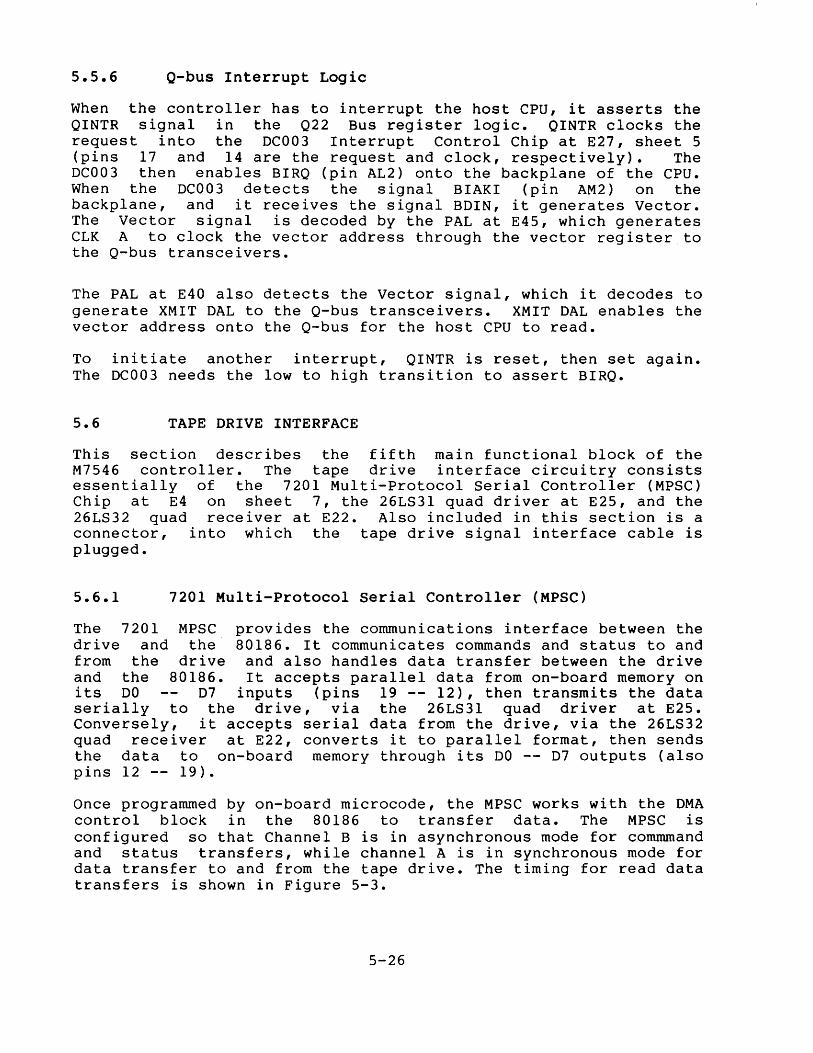
5.5.6 Q-bus Interrupt Logic
When the controller has to interrupt the host CPU, it asserts the QINTR signal in the Q22 Bus register logic. QINTR clocks the request into the DC003 Interrupt Control Chip at E27, sheet 5 (pins 17 and 14 are the request and clock, respectively). The DC003 then enables BIRQ (pin AL2) onto the backplane of the cpu. When the DC003 detects the signal BIAKI (pin AM2) on the backplane, and it receives the signal BDIN, it generates Vector. The Vector signal is decoded by the PAL at E45, which generates CLK A to clock the vector address through the vector register to the Q-bus transceivers.
The PAL at E40 also detects the Vector signal, which it decodes to generate XMIT DAL to the Q-bus transceivers. XMIT DAL enables the vector address onto the Q-bus for the host CPU to read.
To initiate another interrupt, QINTR is reset, then set again. The DC003 needs the low to high transition to assert BIRQ.
5.6 TAPE DRIVE INTERFACE
This section describes the fifth main functional block of the M7546 controller. The tape drive interface circuitry consists essentially of the 7201 Multi-Protocol Serial Controller (MPSC) Chip at E4 on sheet 7, the 26LS31 quad driver at E25, and the 26LS32 quad receiver at E22. Also included in this section is a connector, into which the tape drive signal interface cable is plugged.
5.6.1 7201 Multi-Protocol Serial Controller (MPSC)
The 7201 MPSC provides the communications interface between the drive and the 80186. It communicates commands and status to and from the drive and also handles data transfer between the drive and the 80186. It accepts parallel data from on-board memory on its DO D7 inputs (pins 19 -- 12), then transmits the data serially to the drive, via the 26LS31 quad driver at E25. Conversely, it accepts serial data from the drive, via the 26LS32 quad receiver at E22, converts it to parallel format, then sends the data to on-board memory through its DO -- D7 outputs (also pins 12 -- 19).
Once programmed by on-board microcode, the MPSC works with the DMA control block in the 80186 to transfer data. The MPSC is configured so that Channel B is in asynchronous mode for commmand and status transfers, while channel A is in synchronous mode for data transfer to and from the tape drive. The timing for read data transfers is shown in Figure 5-3.
5-26
SYNC MARK OF THE PREAMBLE
READ DATA
/ ONE CLOCK IS REQUI RED AT THE BEGINNING OF A BLOCK TO SYNC UP THE UART ON THE CONTROLLER
Figure 5-3
2
DATA FIELD
"
I 34568
I ON THE 8th CLOCK AFTER THE SYNC CLOCK THE UART WI LL INTERRUPT THE 80186 WITH A DMA REQUEST
SHR-0223-85
Read Data Timing
On power-up, the MPSC's internal registers are programmed for the configuration already mentioned. The registers are altered during data transfer, to let the MPSC interrupt the 80186. The MPSC interrupts the 80186 under the following conditions:
1. On detection of a read gap. 2. First character received, to start read DMA transfers. 3. Transmit Buffer Empty, to append the CRC on a write to
the tape drive.
The MPSC is programmed so that DMA is enabled each time a byte is required on a write or read. The MPSC asserts a DMA request (pin 11 or pin 32, read and write respectively), to one of the DMA request lines to the 80186, through E2 and E17 (sheet 7) for DMA reads, and E5 and E17 for DMA writes.
The MPSC interrupts the 80186 when it receives the first character, either from the drive or from on-board memory. This is the beginning of the DMA transfer. The sequences for DMA read (data), DMA write (data) follow:
DMA Read
1. The MPSC generates DRIVE DR CMD from its TxDB pin.
2. The MPSC receives a clock (DRIVE RD CLK) on RxCA (pin 35).
3. The MPSC receives serial data from the drive (DRIVE RD DATA) RxDA (pin 34), through E22.
4. The MPSC generates a DMA Read Request (RDYA, pin 32) to the 80186 through E2 and E17.
5. The 80186 responds with DMA HAl through E6 to enable the MPSC.
6. The 80186 asserts RD (MPSC pin 22).
5-27

7. The MPSC sends parallel data via DO -- D7 (pins 19 -- 12) to on-board memory.
8. The MPSC asserts Read DMA Request for each byte, until the 80186 DMA terminal count is reached.
Figure 5-3 shows the timing for a DMA read operation.
DMA Write
1. The MPSC generates a DMA Write Request (from RDYB).
2. The 80186 responds with DMA HAl through E6 to enable the MPSC.
3. The 80186 provides WR (MPSC pin 21) and data on DO -- D7 (MPSC pins 19 -- 12) from on-board RAM.
4. The MPSC ouputs serial characters for write command (DRIVE DR CMD) •
5. The drive provides DRIVE WR CLK for MPSC input RxCA (pin 35) •
6. The 80186 provides DRIVE WR miscellaneous control register.
GATE through the
7. The MPSC provides serial DRIVE WR DATA from TxDA (MPSC pin 37).
8.
5.6.2
The MPSC asserts Write DMA Request for each succeeding byte until an 80186 DMA terminal count is reached.
Differential Drivers and Receivers
There is one differential driver that sends data and commands to the drive and one differential receiver that accepts clocks, data, and status from the drive.
The 26LS31 differential driver at E25 (7-B2) sends the following signals to the drive.
• Serial Drive Write Gate (DRIVE WR GATE) • Serial Drive Erase (DRIVE ERASE) • Serial Drive Commands (DRIVE DR CMD) • Serial Drive Data (DRIVE WR DATA)
5-28

The 26LS32 differential driver at E22 (7-A7, 7-C7) accepts the following signals.
5.7
• • • •
Serial Drive Status (DRIVE DR STATUS) Serial Drive Read Data (DRIVE RD DATA) Drive Read Clock (DRIVE RD CLK) Drive Write Clock (DRIVE WR CLK)
Diagnostic Hardware
The last major section of logic on the M7546 controller is the gates that have been assigned diagnostic functions. The hardware detailed in this section has been specifically provided for diagnostic checking of the various logic elements on the controller.
5.7.1 Diagnostic Indicators
There are two red LEDs on the top edge of the M7546 module. LEDI and LED2, controlled by the 80186 through the miscellaneous control register (Section 5.4.1), signal pass/fail of the on-board microdiagnostics. On power-up, both LEDs light. After the power-up diagnostics have completed, LEDI goes out. LED2 goes out after TMSCP has successfully initialized the controller.
When observing the board from the front with the backplane connectors on the bottom, the LED on the left indicates the diagnostic status and the one on the right indicates the status of the port initialization. If the board is mounted in the BA123-A enclosure, the diagnostic indicator is on the top, and the port initialization indicator is on the bottom.
5.7.2 Miscellaneous Register Loopback
Three signal lines in the miscellaneous read register are for direct diagnostic feedback to the 80186. This is so the register can check that the lines can be set and reset.
• Drive Write Gate
•
•
This signal is set in the miscellaneous write register by the 80186, then checked by the 80186 through the miscellaneous read register.
Drive Erase This signal register and register.
QINTR
is also checked
set in through
This signal is set by the register and checked by miscellaneous read register.
5-29
the the
miscellaneous write miscellaneous read
80186 through the Q22 bus the 80186 through the
5.7.3 7201 MPSC Diagnostic Loopback
The 7201 MPSC chip can be tested without a tape drive connected to the controller. This is accomplished by the 74LS157 quad two-to-one multiplexer at E12 (7-C6). Commands sent by the MPSC are looped back through this mutiplexer as drive status, and write data sent by the MPSC is looped back as read data.
In this mode, the 80186 asserts the signal DIAG in the miscellaneous control register (74LS259 Latch at E35, 4-07). The signal DIAG performs the following functions.
1. DIAG connects write data (from the MPSC's pin 37 -TxDA) , through the MUX (pin 13), to the MPSC's input pin 34 (RxDA). The 80186 sends data out through the MPSC, with DIAG asserted, reads it back through the MPSC, and compares it to the data originally sent. This checks that the MPSC can read and write data through Channel A.
2. DIAG connects drive commands (from the MPSC's pin 8 -TxDB) , around through the MUX (pin 10) to the MPSC's input pin 9 (RxDB) for drive status. The 80186 sends data out through the MPSC's channel B, then, with DIAG asserted, reads it back through the receive section of MPSC Channel B. The 80186 compares the data received to the data sent. This checks that the MPSC can write and read data through its channel B (commands and status during normal operation).
3. When data read/write and command/status diagnostic operations are happening, the 80186 is using DIAG CLK to clock the data to and from the MPSC. This makes sure that the MPSC can accept transmit and receive clocks (Drive Read and Drive Write clocks, respectively, during normal operation).
DIAG CLK can detect counter MPSC can be generating an detected.
also be gated through the MUX to the gap at EIO (7-06). In this configuration, the checked to make sure it is capable of
interrupt when a gap on the tape is
This capability also checks the gap detect counter (EIO) and the gap detect flip-flop at Ell. The counter generates a clock to the gap detect flip-flop on the eighth occurrence of DIAG CLK. The gap detect flip-flop generates the Gap Detect signal (connected to pin 6 of the MPSC). When the MPSC detects the falling edge of Gap Detect, it interrupts the 80186 to inform it of the gap.
5-30
5.7.4 Soft Grounds
For GR and QV testers, the M7546 controller provides resistors to ground on some gates. These can be used by testers to disable these gates for testing. The following are the locations of soft grounds.
1. Page 2 of the schematics. The output enable pins (pin 1) of the 80186 address latches, by a 68 ohm resistor. The enable can be pulled high so the testers can inject any address into the latches.
2. Page 5. The output enable (pin 1) of the 74F374 latches at E9. The testers can pull the enable high to inject any combination of signals into the FPLS.
3. Page 7. Connects the enable signal of the MUX at E12 to ground with a 68 ohm resistor. The testers can pull up the enable signal so they can inject signals into the MPSC to test it.
Figure 5-4 on page 5-32 is a detailed TQK50 block diagram.
5-31
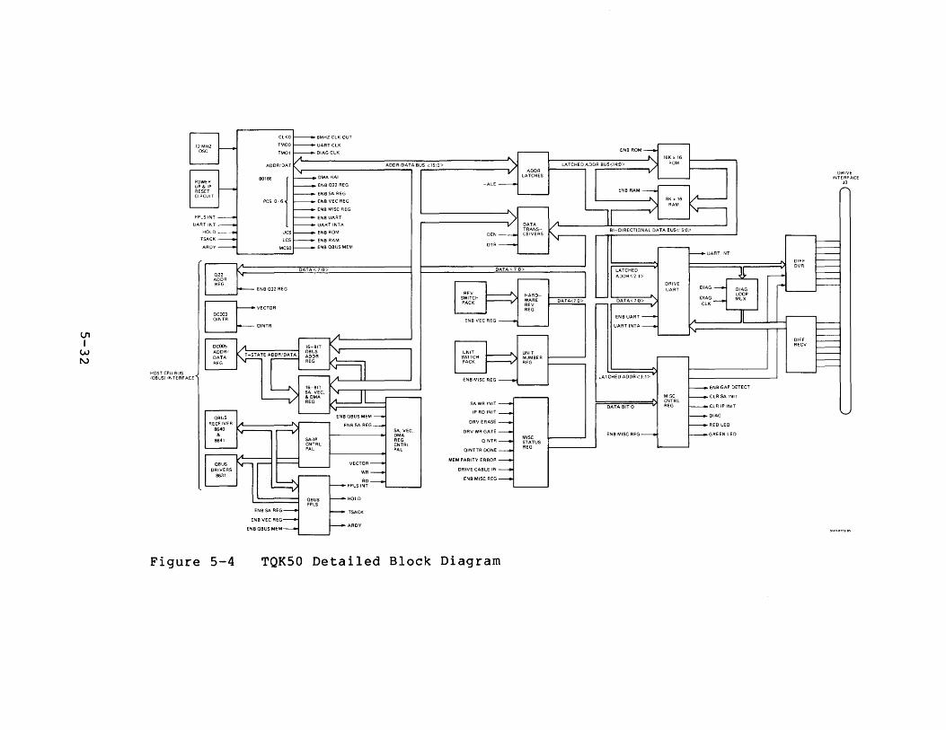
(J1
I w I\.)
HOST CPu BUS lOBUS) INTERFACE
OBUS
6MHZ eLK OUT
UAAT eLK
DIAG CLK
,~ _________________ A_D_D_R/_D~ATABU~S_<_'5_0~> ____________ -'./1
OMA HAl
ENB 022 REG
ENB SA REG
ENB VEC REG
ENB MISC REG
ENB UART
UART INTA
ENB ROM
ENB RAM
ENB oaus MEM
DATA < 7.0>
SA WR IN IT
IP AD IN IT
RECEIVER 1/'-----------' ...... 8640
& 8641
DRV ERASE
DRV WR GATE
OINTR
OINTTR DONE
MEM PARITY ERROR
DRIVE CABLE IN
ENB MISC REG
HOLD
TSACK
ARDY
Figure 5-4 TQK50 Detailed Block Diagram
MISC STATUS REG
DATABITO
EN8 MISC REG
MISC eNTRl REG
ENB GAP DETECT
CLR SA INIT
CLR IP INIT
DIAG
RED LED
GREEN LED
OIFF DVR
DIFF RECV
DRIVE INTERFACE
J3

6.1 GENERAL
CHAPTER 6 TUKSO CONTROLLER
THEORY OF OPERATION
This chapter describes the TKSO Unibus controller (TUKSO). Many of the circuits on this module are similar to the TK50 Q-bus controller (TQKSO) described in Chapter 4. Refer to TUKSO Field Maintenance Print Set, MP-2059, while reading this chapter.
This chapter uses the following format to find a particular component within the Circuit Schematic (CS). The component name and physical location: The PAL at E38. The Circuit Schematic sheet number and location zone: l-C6.
For example, E38 (1-C6) is the PAL at E38, shown on the TUKSO Field Maintenance Print Set, MP-2059, Circuit Schematic sheet 1, ~--~~------~~-------------location zone C6.
NOTE There are several circuits on this module that are virtually identical to module M7S46 (TQKSO). Generally, these circuits encompass the drive interface and address/unit number jumpers and switch packs.
6.2 POWER-UP RESET (MP-20S9, CS, SHEET 1)
The activation of BUS DC LO L or BUS IN IT L causes a signal to be asserted at pin 13 of the 16L8 logic array (E38, l-C6). (See Figure 6-1.). The output of the array (pin 12) is applied to counter E68 (l-DS), which generates MICRO RESET L. The counter counts up to eight and resets the 80186 microprocessor (E90, 2-C5) and the Field Programmable Logic Sequencer (FPLS), (E61, 8-C5), that operates the Unibus circuitry.
The previously discussed counter reset circuitry is also used when the CPU writes to the IP register. This ensures a proper reset of all the circuitry on the board as required by TMSCP. The resetting of the board by writing the IP register is part of the Unibus/Q-bus Port Protocol (see U/Q Port Control Specification and Section 6.9.2 of this document).
6-1

BUS DC LOL
BUS INIT L
E38 LOGIC ARRAY
12 1
E68 BINARY COUNTER CLEAR
15
.-------.... MICRO RESET L
INITH
SH R-0007-86
Figure 6-1 Power Up Reset Circuitry
6.3 MICROPROCESSOR CYCLE TIME (MP-2059, CS, SHEET 2)
The processor cycle time is derived from a 12 MHz crystal oscillator (E89, 2-A7), which is connected through inverter E94 to pin 59 of the 80186 microprocessor (Figure 6-2). The 80186 divides the 12 MHz signal by 2, resulting in a CLK/2H signal (E90, pin 56) of 6 MHz. This corresponds to 166 ns per clock. Since a bus cycle consists of four clocks, its duration is 166 ns x 4, or 664 ns per cycle.
6.3.1 Memory Chip Select Lines (MP-2059, CS, Sheets 2 and 3)
The 80186 microprocessor contains a memory chip select unit that is programmed when power is applied. The unit consists of the following six memory chip select lines and their corresponding addresses.
LMCS (lower memory chip select) MCSO (memory chip select 0) MCSl (memory chip select 1) MCS2 (memory chip select 2) MCS3 (memory chip select 3) UMCS (upper memory chip select)
NOTE
00000-03FFF (RAM) 4000-5FFF 6000-7FFF 8000-9FFF AOOO-BFFF F8000-FFFFF (EPROM)
MCS1, MCS2, and MCS3 are not used. The LMCS is connected to the RAM chips (E53 and E54) from pin 33 of the 80186 and is designated ENS RAM L.
The UMCS is connected to the ROM chips (E48 and E49) from pin 34 of the 80186 and is designated ENB ROM L (Figure 6-3).
6-2

6.3.2
E89 12 MHz OSCILLATOR CLK
Figure 6-2
E90 80186 MICRO· PROCESSOR
80186 MICRO· PROCESSOR E90
56
E85 COUNTER
'----+ CLK/2 H
S H R ·0008·86
Microprocessor Timing Circuit (MP-2059, CS, Sheet 2)
E48 E49 EPROM EPROM
UCS 34 ENS ROM L 1 T
LCS 33 ENS RAM L .-
Figure 6-3
1 ~ E53 E54 8K 8K RAM RAM
SHR·0009·86
Memory Chip Select Lines (MP-2059, CS, Sheets 2 and 3)
Peripheral Chip Select Lines
The 80186 microprocessor has seven peripheral chip select lines to access external devices such as Input/Output (I/O) ports or registers. These peripheral chip select lines are memory mapped on the M7547 for fast interrupt servicing.
The hexadecimal memory-mapped locations for these lines follow.
PCSO PCSl PCS2 PCS3 PCS4 PCS5 PCS6
F800-F87F F880-F8FF F900-F97F F980-F9FF FAOO-FA7F FABO-FAFF FBOO-FB7F
6-3

The peripheral chip select lines control the following functions.
PCSO
PCSl
PCS2
PSC3
PCS4
PCSS
PCS6
Enables writing and reading to the 7201 Multi-Protocol Serial Controller (MPSC) control registers.
Acknowledges read and write direct memory access (DMA) operations from the 7201.
Enables writing to the second miscellaneous register MISC2, to load FPLS commands, clear error conditions, load word counts, and so on.
Enables reading and writing of data from the SA register.
Enables reading of the hardware revision and unit number switches.
Enables writing to the miscellaneous control register and reading of the miscellaneous status register.
Reserved
The signal names given to the peripheral chip select lines are shown in Figure 6-4.
E90 80186 MICRO-PROCESSOR
PC36/A2 32 RESERVED
PC35/Al 31 ENB MISC REG L
PCS4 30 ENB SWITCH L
PCS3 29 ENB SA REG L
PCS2 28 ENB MISC2 REG L
PCSl 27 DMA HAl L
PCSO 25 ENB UART L
SH A-DOl 0-86
Figure 6-4 Peripheral Chip Select Lines (MP-20S9, CS, Sheet 2)
6-4

6.3.3 Peripheral Control Block
The peripheral control block defines how the 80186 is programmed with respect to the following functions.
• Memory mapping or I/O mapping
• DMA transfers
• Timer/counters
• Chip select boundaries
• Interrupt status
The peripheral control block can be read from or written to at anytime. The peripheral control block resides in the following microprocessor memory range.
OFFOO -- OFFFF
For further information on peripheral control block programming, see the TMSCP Controller Firmware Specification.
6.3.3.1 Internal and External Interrupts -- The 80186 interrupt controller is in the peripheral control block. There are two types of interrupts: internal and external. The following are examples of internal interrupts.
• Reaching DMA terminal count, or • Reaching the maximum count of a timer/counter.
The following are examples of external interrupts.
• The 7201 MPSC interrupt, which occurs when the 7201 is communicating with the drive.
• An FPLS interrupt of a Unibus DMA transfer error, such as Unibus memory parity error or nonexistent memory error.
The 7201 MPSC asserts UART INT H through the 7414 inverter at E94 (9-83). When UART INT H is asserted at pin 44 of the 80186, the 80186 responds by asserting its INTAI line (pin 41). This response is the interrupt acknowledge signal (UART INTA). The 80186 is configured in cascade mode for assertions of its INTI line, so it gives two interrupt acknowledge pulses (INTAs) to the MPSC. The first INTA from the 80186 acknowledges receipt of the interrupt and tells the MPSC that it is being serviced. The second INTA tells the MPSC to place its interrupt vector on the 80186's data bus (DATA7:0). The MPSC can supply vector addresses for interrupt routines to the 80186.
6-5

E90 80186 MICRO· PROCESSOR
PCS2 ENB MISC2 REG L
SHEET 2
E33 1 OF 8 DECODER
SHEET 4
E27 PARITY CHECK F/F
SHEET 7
CLR PAR ERROR L
CLR NXM L
E27 NXM F/F
PARITY ERROR H
SHEET NXM H 6
SHR·OOll·86
Figure 6-5 FPLS Interrupt (MP-2059, CS, Sheets 2,4,6,&7)
The second type of external interrupt, which occurs through the FPLS, is not responded to with an INTA by the 80186. This is because the 80186 is programmed in noncascade mode for assertion of its INT2 line (pin 42). This mode does not supply any interrupt acknowledge pulses in response to an interrupt. PCS2, which is labeled ENB MISC2 REG, resets the memory parity error flip-flop (E27, pin 13 7-B6), and clears the NXM error flip-flop (E27, pin 4 -- 6-01) (Figure 6-5).
There is also a nonmaskable interrupt (NMI) to the 80186 on E48, pin 6. This signal monitors ACLO (CV1) on the backplane of the CPU, and is an early indication that power is going down and that the 80186 should take the appropriate steps to power-down cleanly.
6.3.3.2 Counter/Timers The 80186 has three general purpose counter/timers. The counters are configured in the peripheral control block. Timer 0 and 1 both have count enable inputs (E90, pins 20 and 21). The inputs are always enabled. Timer 2 is an internal-only firmware timer. Its external pins are not connected.
6-6
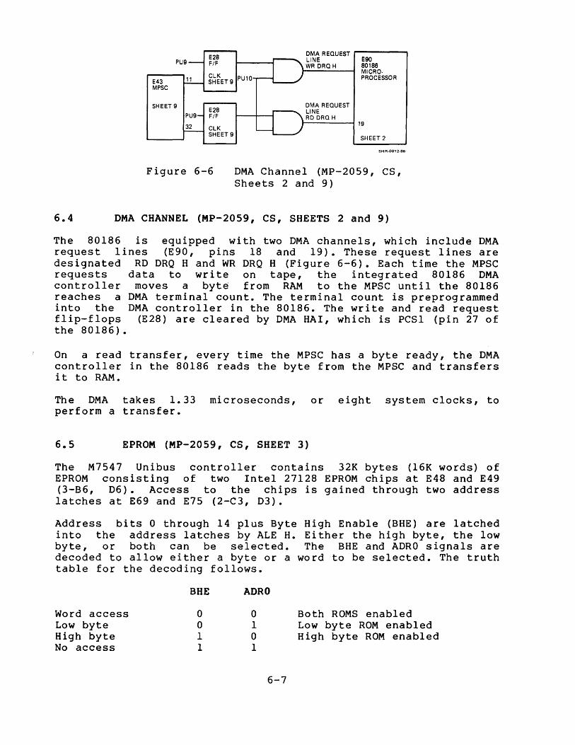
E28 F/F
OMA REQUEST ,.......---LINE E90 WR ORQ H 80186
E43 MPSC
~~~ET 9 PU10 MICRO· PROCESSOR
SHEET 9
PU9 E28 F/F
32 CLK SHEET 9
Figure 6-6
OMA REQUEST LINE RO ORQ H t-------i 19
SHEET 2
SH R-OO' 2-86
DMA Channel (MP-2059, CS, Sheets 2 and 9)
6.4 DMA CHANNEL (MP-2059, CS, SHEETS 2 and 9)
The 80186 is equipped with two DMA channels, which include DMA request lines (E90, pins 18 and 19). These request lines are designated RD DRQ Hand WR DRQ H (Figure 6-6). Each time the MPSC requests data to write on tape, the integrated 80186 DMA controller moves a byte from RAM to the MPSC until the 80186 reaches a DMA terminal count. The terminal count is preprogrammed into the DMA controller in the 80186. The write and read request flip-flops (E28) are cleared by DMA HAl, which is PCSI (pin 27 of the 80186).
On a read transfer, every time the MPSC has a byte ready, the DMA controller in the 80186 reads the byte from the MPSC and transfers it to RAM.
The DMA takes 1.33 microseconds, or eight system clocks, to perform a transfer.
6.5 EPROM (MP-2059, CS, SHEET 3)
The M7547 Unibus controller contains 32K bytes (16K words) of EPROM consisting of two Intel 27128 EPROM chips at E48 and E49 (3-B6, D6). Access to the chips is gained through two address latches at E69 and E75 (2-C3, D3).
Address bits 0 through 14 plus Byte High Enable (BHE) are latched into the address latches by ALE H. Either the high byte, the low byte, or both can be selected. The BHE and ADRO signals are decoded to allow either a byte or a word to be selected. The truth table for the decoding follows.
Word access Low byte High byte No access
BHE ADRO
o o 1 1
o 1 o 1
6-7
Both ROMS enabled Low byte ROM enabled High byte ROM enabled

The 80186 reads data from the ROM through two data transceivers (E74 and E81, 2-C2, D2). The Data Enable (DEN) signal from pin 39 of the 80186 enables the transceivers.
6.6 RAM (MP-2059, CS, SHEET 2)
The random access memory (RAM) consists of two 8K by 8 static RAM chips. Like the EPROMs, access to the RAM chips is gained through the address (E69 and E75) and data (E74 and E81) transceivers. Unike the EPROMs, which can only be read, the data transceivers can be activated in either direction by the DTR signal.
The RAM chips connect through the transceivers to the 80186 microprocessor,. SHE and ADRO access the high and low bytes of the RAM by the same method described for the EPROM (see Section 6.5).
The RAM memory access time is 150 ns.
6.7 CONTROL AND STATUS REGISTERS
The M7547 Unibus controller uses the following registers.
• Miscellaneous control register
• Status register
• Hardware and unit number switch registers
• SA register
• IP register
These registers are described in the following paragraphs.
6.7.1 Miscellaneous Control Register (Write)
There are two types of miscellaneous control registers on the M7547: read and write. The bits in the miscellaneous write registers are addressable on word boundaries. They are set or reset by writing to an address within the range of PCS5 (FASO-FAFF) or PCS2 (F900-F97F) for the functions shown in Tables 6-1 and 6-2.
This register is reset by INIT during power-up or when the host is writing the IP register. To set a bit in this register, DATAO must be asserted when writing to the address containing the bit to be set. To reset a bit in this register, DATAO must be negated when writing to the address containing the bit to be reset. All the signals controlled by this register are true when high. The following bits and addresses are associated with this register.
6-8

Table 6-1
Address
FA80 FA82 FA84 FA86 FA88 FA8A FA8C FA8E
Table 6-2
Address
F90X F91X F92X F93X F94X F9SX F96X F97X
Miscellaneous Write Register One (E35) -- PCSS
Bit
Drive erase Drive write gate Enable gap detect Diagnostic mode Reset LED 1 Reset LED 2 Reset LED 3 Reset LED 4
Miscellaneous Write Register Two (E33) -- PCS2
Bit
Clear SA write Clear IP read Clear nonexistent memory flag Clear parity error flip-flop Load lower Unibus DMA address (bits 15:0) Load upper Unibus DMA address (bits 16,17) Load DMA word count Load FPLS command
6.7.1.1 Drive Erase -- The drive erase bit signals the drive to start erasing to put gaps between blocks on the tape. For the erase bit to work, the drive write gate must be set and the tape cartridge cannot be write protected. If the cartridge is write protected, the drive returns an error status to the controller, informing the controller that the cartridge is write protected.
6.7.1.2 Drive Write Gate -- The drive write gate bit signals the drive to start writing data or to erase tape. The drive only writes if the tape cartridge is not write protected. If the cartridge is write protected, the drive returns an error message to the controller.
6-9

6.7.1.3 signal, register through
Enable Gap Detect (Circuit Schematics, Sheet 9) -- This when asserted, enables a 1 to be shifted into the shift
(E24). Each time a write clock occurs, a 1 is shifted the shift register until eight clocks have occurred. This
the gap detect flip-flop (E21) to toggle, which in turn, a transition on pin 6 of the serial controller (E43). (See
6-7. )
causes causes Figure
NOTE If a read clock or IN IT occurs during the time the eight write clocks are being input to the shift register, the shift register resets. This is shown by gate £29, the output of which is applied to the clear input (pin 9) of the shift register.
The transition, which can be low to high or high to low, causes the serial controller to interrupt the 80186 microprocessor. The interrupt signals the 80186 that a gap on the tape has been detected.
6.7.1.4 Diagnostic Mode -- When the diagnostic mode bit is set, it enables the loopback diagnostic multiplexer (E30) and disables the drive line drivers (E70). This allows the loopback diagnostic to be run to check the MPSC and the gap detect circuit.
E24 E21 GAP 2 12 SHIFT DETECT
REGISTER ENB GAP DET H---I
DRIVE RD ClK
DIAG ClK H
DRIVE WR ClK H
INIT
E30 2 INPUT MUlTIPLEX
Z8
SHEET 9
GAP OATH
6
Figure 6-7
F/F
7 OAT ClR 6
5 11 SHEET 9
SHEET 9 4 ClK 3 2
8 ClK 1 0
E43 E90 MUlTI-
PROTOCOL MICRO-SERIAL PROCESSOR UART INTA l CONTROllER
44
SHEET 9 SHEET 2
SH R-0013-86
Enable Gap Detect Circuit (MP-2059, CS, Sheets 2 and 9)
6-10

6.7.1.5 Reset LEDs 1-4 The controller contains four red on-board status LEDs for fault and on-line indication. All LEDs are turned on at power-up, and remain on until successful completion of the resident microdiagnostics. When the power-up diagnostic hassuccessfully completed, LEDs 2, 3 and 4 go off, leaving LED lon, indicating step 1 of U/O Port initialization. LEDs 2, 3 and 4 are turned on and off for each of the respective U/O Port initialization steps. All LEDs turned off indicates that the controller has successfully completed the U/O Port initialization sequence and has been placed on-line by the host. All four LEDs are mounted on the board edge for maximum visibility.
When a failure is detected, an error code is posted in the SA register, providing the hardware is functional enough to permit it. Error codes are either port generic or controller specific. The microprocessor is forced into an infinite loop-type instruction sequence that can be broken only by receiving an initialization from the host. There are no detectable failures possible that would warrant automatic retries be performed.
6.8 STATUS REGISTER (MISCELLANEOUS READ REGISTER)
The status register is a 16-bit buffer (E34, E42) shown on page 4 of the Circuit Schematics. The register is enabled by ENB MISC REG Land DTR H. The ENB MISC REG L signal is peripheral controller select 5 (see Section 6.3.2). The DTR determines whether the direction of the data is for a read or a write operation. When DTR H is negated, the DMX word count and status of the controller board can be read by the 80186 microprocessor. The following chart names and details each bit in the status register.
DATA DATA DATA DATA DATA DATA DATA DATA
DATA DATA DATA DATA DATA DATA DATA DATA
0 1 2 3 4 5 6 7
8 9 10 11 12 13 14 15
SA write IP read Drive erase Drive write gate DMA stop count bit FPLS command done Host memory parity error Host address overflow error
LSB
Host DMA word count
MSB
6-11

SA write
IP read
Drive erase
Drive write gate
DMA stop count bit
FPLS command done
Host memory parity error
Host address overflow error
Host DMA wcount
Indicates that the host processor has written the SA register.
Indicates that the host has read the IP register.
Indicates diagnostic loopback for the write miscellaneous control register. Drive erase is asserted and the controller senses the signal to ensure that it is asserted.
Indicates diagnostic loopback for the write miscellaneous control register. Drive write gate is asserted and the controller senses the signal to make sure that it is asserted.
Indicates that a DMA transfer is complete.
Asserted by the FPLS to indicate that a Unibus transfer has been completed.
Indicates that a parity error has occurred and the Unibus transfer has not successfully completed.
Indicates error has transfer completed.
that an address overflow occurred and the Unibus
has not successfully
Indicates how any words are in the DMA buffer.
6.9 STATUS/ADDRESS REGISTER
The SA register (part of the U/Q Port Protocol) initializes the controller and returns status to the CPU.
The initialization done by this register sends to the controller the vector address command and response ring address, as well as information regarding the length of these rings. The status returned through this register includes unit number and hardware revisions.
6-12

6.9.1 SA Register
The SA register is on page 7 of the Schematics and consists of four 4-bit multifunction registers (El, E7, E13, and E19). The PAL (E38 on page 1) controls the loading and unloading of this register. The SA register is a bidirectional, latched register that can be loaded and enabled in either direction. This means that the 80186 can write to one register and the Unibus can read it or the Unibus can write to the other register and the 80186 can read it.
The 80186 writes to the SA register by decoding the signals ENB SA REG and RAM WR. ENB SA REG logic is shown on sheet 2 of the schematics and RAM WR logic is shown on sheet 3 of the schematics. The 80186 reads the register by decoding ENB SA REG and RD L. RD L logic is shown on sheet 2 of the schematics. For the host CPU to write to the SA register, the signal HOST SAWR is generated by the PAL (E38).
For the host CPU to read the SA register, the signal UBUS XMT is generated by the PAL (E38).
After a write to the IP register or on power-up, the CPU always reads zero from the SA register, until the 80186 loads it with the correct SA register value. The CPU reads zeros at this time because the SA register is not enabled onto the Unibus until the 80186 writes to it. The signal that accomplishes this is UBUS XMT generated by the PAL (E38 on sheet 1 of the schematics). For further information on the SA register chip, refer to the 1983 Advanced Micro Devices Bipolar Data Book. For further information on the SA register, refer to the U/Q Port Protocol Specification.
6.9.2 IP Register
The IP register is logically part of the TMSCP protocol, but is not a physical register. The controller board has only to decode that the CPU has either written to or read from the IP register I/O address on the Unibus.
The PAL (E38 on page 1 of the schematics), decodes that the IP register has been selected by the signals MATCH, SA/IP ADR 1, and RMSYN. Similarly, the selection of the SA register is decoded.
When the host CPU does a read of the IP register, the PAL generates the flag HOST IP RD, which the 80186 can read through the miscellaneous read register. The 80186 then takes the appropriate action according to the U/Q Port Protocol.
This flag stays set until the 80186 clears it by the signal CLR IP RD.
6-13

When the CPU does a write to the IP register, the PAL generates the strobe used to set the power-up reset circuitry.
This resets the controller board as part of the U/Q Port Protocol. For further information on the IP register, refer to the U/Q Port Protocol Specification.
6.10 Tape Drive Interface
The next main functional block on the M7547 controller is described in this section. The Tape Drive Interface Circuitry is comprised of the Intel 7201 Multi-Protocol Serial Controller (MPSC) Chip at E43 on sheet 9, the 26LS31 driver at E70, and the 26LS32 receiver at E36. Also included in this section is a connector, into which the tape drive signal interface cable is plugged.
6.10.1 7201 Multi-Protocol Serial Controller (MPSC)
The 7201 drive and and from drive and
MPSC provides the communication interface between the the 80186. The MPSC communicates commands and status to the drive and also handles data transfer between the the 80186. It accepts parallel data from on-board
memory on its DO-D7 inputs (pins 19-12), then sends the data serially to the drive, through the 26LS31 quad driver at E25. Conversely, the 7201 MPSC accepts serial data from the drive, through the 26LS32 receiver at E36, converts it to parallel format, then sends the data to on-board memory through its DO-07 outputs (also pins 12-19).
Once programmed by on-board microcode, the MPSC works with the DMA control block in the 80186 to transfer data. The MPSC is configured so that Channel B is in asynchronous mode for commmand and status transfers, while channel A is in synchronous mode for data transfer to and from the tape drive.
On power-up, the MPSC's internal registers are programmed for the previously discussed configuration. The registers are altered during data transfer, to let the MPSC interrupt the 80186. The MPSC interrupts the 80186 under the following conditions.
1. On detection of a read gap. 2. First character received, in order to start read DMA
transfers. 3. Transmit Buffer Empty, in order to append the CRC on a
write to the tape drive.
The MPSC is programmed so that DMA is enabled each time a byte is needed on a write or read. For DMA read and writes, the MPSC asserts a DMA request (pin 11 or pin 32, read and write respectively), to one of the DMA request lines to the 80186, through E22, E28, and E29 (sheet 9).
6-14

The MPSC interrupts the 80186 when it receives the first character, either from the drive or from on-board memory. This is the beginning of the DMA transfer. The sequences for DMA read (data) and DMA write (data) follow.
DMA Read
1. The MPSC generates DRIVE DR CMD from its TxDB pin.
2. The MPSC receives a clock (DRIVE RD CLK) on RxCA (pin 35) •
3. The MPSC receives serial data from the drive (DRIVE RD DATA) RxDA (pin 34), through E30.
4. The MPSC generates a DMA Read Request (RDYA, pin 32) to the 80186 through E22, E28, and E29.
5. The 80186 responds with DMA HAl through E29 to enable the MPSC.
6. The 80186 asserts RD (MPSC pin 22).
7. The MPSC sends parallel data through DO-D7 (pins 19-12) to on-board memory.
8. The MPSC asserts Read DMA Request for each byte, until the 80186 DMA terminal count is reached.
DMA Write
1. The MPSC generates a DMA Write Request (from RDYB) •
2. The 80186 responds with DMA HAl through E29, to enable the MPSC.
3. The 80186 provides WR (MPSC pin 21) and data on DO-D7 (MPSC pins 19-12) from on-board RAM.
4. The MPSC ouputs serial characters for write command (DRIVE DR CMD).
5. The drive provides DRIVE WR CLK for MPSC input RxCA (pin 35) •
6. The 80186 provides DRIVE WR miscellaneous control register.
GATE through the
7. The MPSC provides serial DRIVE WR DATA from TxDA (MPSC pin 37).
8. The MPSC asserts WR DMA REQ for each succeeding byte until an 80186 DMA terminal count is reached.
6-15
6.10.2 Differential Drivers and Receivers
There is one differential driver that sends data and commands to the drive. There is one differential receiver that accepts clocks, data, and status from the drive.
The 26LS31 differential driver at E70 (9-82) sends the following signals to the drive.
• Serial Drive Write Gate (DRIVE WR GATE) • Serial Drive Erase (DRIVE ERASE) • Serial Drive Commands (DRIVE DR CMD) • Serial Drive Data (DRIVE WR DATA)
The 26LS32 differential driver at E36 (9-87) accepts the following signals from the drive.
6.11
• • • •
6.11.1
Serial Drive Status (DRIVE DR STATUS) Serial Drive Read Data (DRIVE RD DATA) Drive Read Clock (DRIVE RD CLK) Drive Write Clock (DRIVE WR CLK)
UNIT NUMBERING AND I/O ADDRESSING
Module Starting Addresses/Interrupt Vectors
Any M7547 module you install must be set to the correct starting address and interrupt vector. The interrupt vector is set to 260 under program control. The vector for additional TK50 modules installed in the system becomes a floating vector, which is also set under program control.
The starting address of the first tape controller is fixed at 774500. Currently, there are two TMSCP devices -- TK50 and TU81 -that can be assigned the fixed address of 774500, depending on system implementation. All other TK50 TMSCP devices are installed in a floating address space of 760nnn (octal). The floating address space is set using the address jumpers on the M7547 module. Other TK50 devices are assigned other floating addresses based on system configuration. For example, if there are three TK50s in a system with no TU81, the first TK50 is assigned the fixed address of 775400, the second 760404, and the third 760444. Table 6-3 shows the jumper connections for these addresses. Figure 6-8 shows the jumper settings for the fixed 774500 address.
6-16
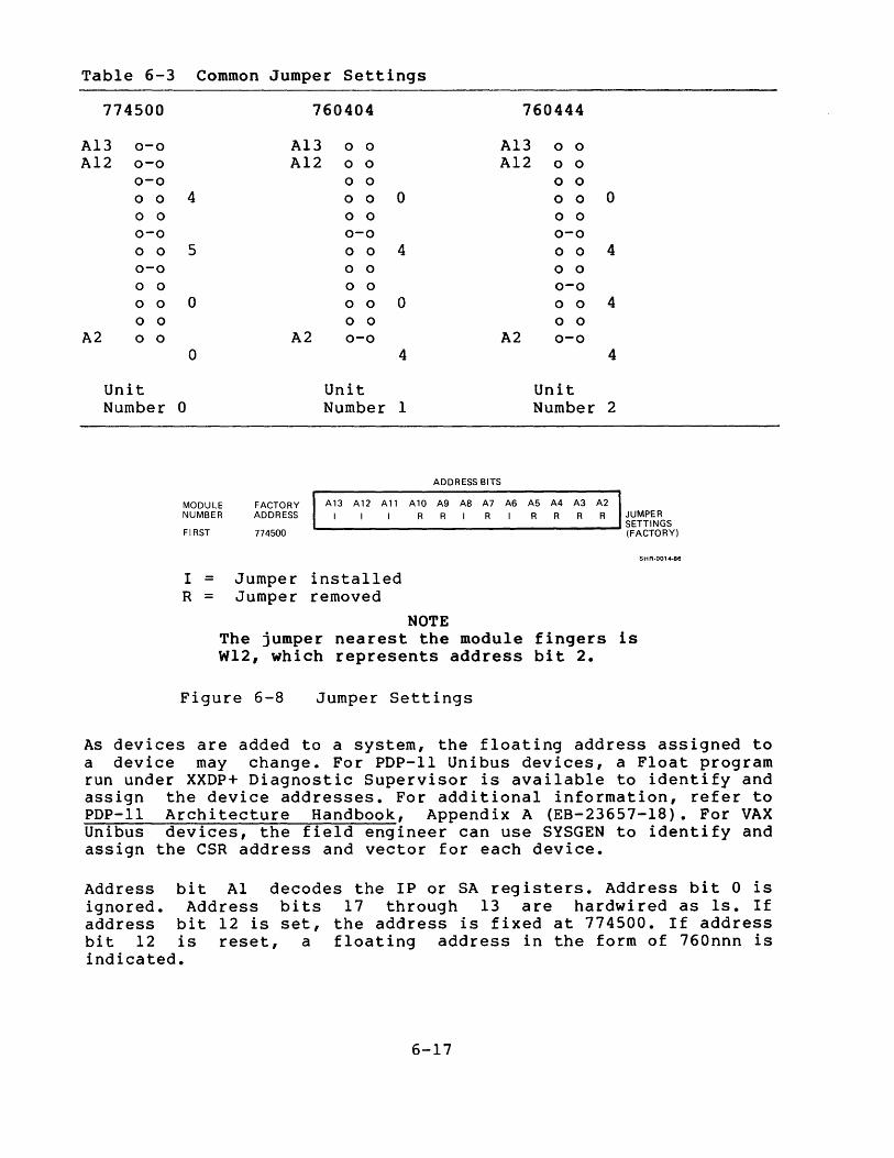
Table 6-3
774500
A13 0-0
A12 0-0
0-0
o 0
0 0 0-0
0 0 0-0
0 0 o 0
0 0 A2 o 0
Unit Number
Common Jumper Settings
4
5
0
0
0
MODULE NUMBER
760404 760444
A13 o 0 A13 o 0 A12 o 0 A12 o 0
o 0 o 0
0 0 0 0 0 0 o 0 o 0 0-0 0-0
0 0 4 o 0 4 o 0 o 0 o 0 0-0
0 0 0 o 0 4 0 0 o 0
A2 0-0 A2 0-0
4 4
Unit Unit Number 1 Number 2
ADDRESS BITS
FACTORY ADDRESS
A13 A12 A11 A10 A9 AS A7 A6 A5 A4 A3 A2
I R R I R R R R R
FIRST 774500
JUMPER SETTINGS
'------------------ (FACTORY)
I = Jumper installed R = Jumper removed
NOTE The jumper nearest the module fingers is W12, which represents address bit 2.
Figure 6-8 Jumper Settings
SH R-0014-B6
As devices are added to a system, the floating address assigned to a device may change. For PDP-II Unibus devices, a Float program run under XXDP+ Diagnostic Supervisor is available to identify and assign the device addresses. For additional information, refer to PDP-II Architecture Handbook, Appendix A (EB-23657-18). For VAX Unibus devices, the field engineer can use SYSGEN to identify and assign the CSR address and vector for each device.
Address bit Al decodes the IP or SA registers. Address bit 0 is ignored. Address bits 17 through 13 are hardwired as Is. If address bit 12 is set, the address is fixed at 774500. If address bit 12 is reset, a floating address in the form of 760nnn is indicated.
6-17

6.11.2 Unit Number Dip Switch (E4, 4-87)
The unit number DIP switch must be set to correspond to the address jumper setting. The first setting in Table 6-4 shows the unit number factory setting that matches the starting address jumper setting of 774500.
Table 6-4 Unit Number Switch Pack Settings
Jumper Set Unit Number for an Switch Pack Bits Address 1 2 3 4 5 6 7 8 Unit Number Name
774500 0 0 0 0 0 0 0 0 MUO (first TK50) 760nnn 1 0 0 0 0 0 0 0 MUI (second TK50) 760nnn 0 1 0 0 0 0 0 0 MU2 (third TK50) 760nnn 1 1 0 0 0 0 0 0 MU3 (fourth TK50)
o = Switch open 1 = Switch closed
6.11.3
NOTE Pressing a switch on the open side turns the switch off (Ole Pressing a switch on the opposite side turns the switch on (1) •
Revision Level Dip Switch (E5, 4-C7)
Make sure the revision level DIP switch matches the revision level stamped on the back of the module (see Tables 6-5 and 6-6).
6-18

Table 6-5
Revision Level Number
0 1 2 3 4 5
0 = Switch 1 = Switch
Table 6-6
Revision Level Number
0 1 2 3 4 5
Revision Level Dip Switch
Switch Bits 1 2 3 4 5 6 7 8
0 0 0 0 0 0 0 0 1 0 0 0 0 0 0 0 0 1 0 0 0 0 0 0 1 1 0 0 0 0 0 0 0 0 1 0 0 0 0 0 1 0 1 0 0 0 0 0
open closed
NOTE Pressing a switch on the open side turns the switch off (0). Pressing a switch on the opposite side turns the switch on
Revision Level Switch Pack
Switches 1 2 3 4 5 6 7 8
0 0 0 0 0 0 0 0 1 0 0 0 0 0 0 0 0 1 0 0 0 0 0 0 1 1 0 0 0 0 0 0 0 a 1 a a a a 0 1 0 1 0 0 0 0 0
0 = Switch open 1 = Switch closed
Rev Level a Rev Level 1 Rev Level 2
1 - Off 1 - On 1 - Off 2 - Off 2 - Off 2 - On 3 - Off 3 - Off 3 - Off 4 - Off 4 - Off 4 - Off 5 - Off 5 - Off 5 - Off 6 - Off 6 - Off 6 - Off 7 - Off 7 - Off 7 - Off 8 - Off 8 - Off 8 - Off
6-19

A-I
APPENDIX A TKSO EXPLODED VIEW

Figure A-I TK50 Exploded View
A-2
~INTERPOSER HERE (NOT SHOWN)
~CARTRIDGE RELEASE HANDLE
/FRONT / BEZEL
SH R-0160-85

APPENDIX B TKSO SUBSYSTEM ERROR CODES AND STATUS
This Appendix lists error and status codes sent from the TK50 controller to the host system.
Table B-1 Drive Error Sub-code Values
Subcode
1
2
3
4
Code + Sub-code Dec Oct Hex
43 53 28
75 113 4B
107 153 68
139 213 8B
E S V T
* *
* *
* *
* *
8-1
Status or Event Sub-Code
Drive command timeout. The controller has timed out a command exchange with the drive.
Controller detected ~ransmission error. The controller has detected a protocol violation during a command exchange with the drive.
Recoverable drive fault The drive has detected and reported a recoverable fault during a transfer operation.
Unrecoverable drive fault The drive has detected and reported an unrecoverable fault during a transfer operation.

Table B-2 Controller Internal Status Byte
Value Dec Oct Hex Controller Internal Status
0 0 0 Done 2 2 2 Retry 4 4 4 Hard Error 6 6 6 Tape Mark Read 8 10 8 Logical EOT Detected
10 12 A End of Media 12 14 C Drive Error 14 16 E Communications Exception 16 20 10 End of Data 18 22 12 Failed to Find Append Target 20 24 14 Leaving EOT Trailer Region 22 26 16 ECC Correction on Data 24 30 18 ECC Correction on Tape Mark 26 32 1A BOT Encountered 28 34 1C Data Synchronization Error 30 36 IE EOT detected 32 40 20 Seek Aborted 34 42 22 Unload
Table B-3 Drive Error Code Byte
Value Dec Oct Hex Drive Error Code
1 1 1 Hardware Write Protect 2 2 2 Drive Fault 4 4 4 Communications Exception 6 6 6 Wrong Track
16 20 10 Sync Failure 19 23 13 Communications Error 34 42 22 Positioning Error 35 45 23 Channel B Overrun 39 47 27 Channel A Overrun
B-2
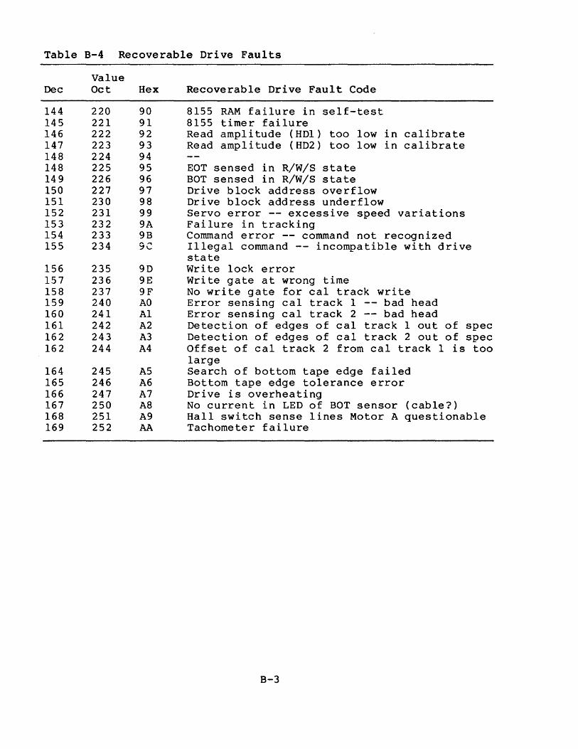
Table B-4 Recoverable Drive Faults
Dec
144 145 146 147 148 148 149 150 151 152 153 154 155
156 157 158 159 160 161 162 162
164 165 166 167 168 169
Value Oct Hex
220 90 221 91 222 92 223 93 224 94 225 95 226 96 227 97 230 98 231 99 232 9A 233 9B 234 9C
235 90 236 9E 237 9F 240 AO 241 Al 242 A2 243 A3 244 A4
245 A5 246 A6 247 A7 250 A8 251 A9 252 AA
Recoverable Drive Fault Code
8155 RAM failure in self-test 8155 timer failure Read amplitude (HOI) too low in calibrate Read amplitude (HD2) too low in calibrate
EOT sensed in R/W/S state BOT sensed in R/W/S state Drive block address overflow Drive block address underflow Servo error -- excessive speed variations Failure in tracking Command error -- command not recognized Illegal command -- incompatible with drive state Write lock error Write gate at wrong time No write gate for cal track write Error sensing cal track 1 -- bad head Error sensing cal track 2 -- bad head Detection of edges of cal track lout of spec Detection of edges of cal track 2 out of spec Offset of cal track 2 from cal track 1 is too large Search of bottom tape edge failed Bottom tape edge tolerance error Drive is overheating No current in LED of BOT sensor (cable?) Hall switch sense lines Motor A questionable Tachometer failure
B-3

Table 8-5 Unrecoverable Drive Faults
Value Dec Oct Hex Unrecoverable Drive Fault Code
129 201 81 Failure to load to BOT 130 202 82 Failure to unload tape into cartridge 131 203 83 General motor or tach failure 132 204 84 Motor A failure 133 205 85 Motor B failure 134 206 86 Drive lost control of tape or bad tach 135 207 87 Excessive drag in tape transport 136 210 88 Failure to stop tape or remain stopped 137 211 89 Cartridge insert error 138 212 8A Cartridge extract error 139 213 8B CU attempted to move tape with drive in error 140 214 8C Deceleration timeout error 141 215 80 Second attempt to balance reels in init
failed
Table B-6 Drive Flags
Bit Bit Mask Number Oct Hex Drive Flags
0 1 1 Cartridge Present 1 2 2 Head at Track Zero 2 4 4 Tape Unloaded 4 10 8 Hardware Write Protected 5 20 10 Positioned at BOT 6 40 20 Drive in Run State
Note: Bits 5 and 6 together indicate that the drive is rewinding to BOT
B-4

Table B-7 UfO Port Generic SA Error Codes
Dec
1 2 3 4 5 6 7 8 9
10
11 12 13 14 15 16
17
18 19 20 21 22
23
Value Oct Hex
1 1 2 2 3 3 4 4 5 5 6 6 7 7
10 8 11 9
12 A
13 B 14 C 15 D 16 E 17 F 20 10
21 11
22 12 23 13 24 14 25 15 26 16
27 17
Failure Code
Envelope/Packet Read (parity or timeout) Envelope/Packet Write (parity or timeout) Controller ROM and RAM parity Controller RAM parity Controller ROM parity Queue Read (parity or timeout) Queue Write (parity or timeout) Interrupt Master Host Access Timeout (higher level protocol dependent) Credit Limit Exceeded (reporting this condition optional) Bus Master Error Diagnostic Controller Fatal Error Instruction Loop Timeout Invalid Connection Identifier Interrupt Write Error MAINTENANCE READ/WRITE Invalid Region Identifier MAINTENANCE WRITE Load to non-Ioadable controller Controller RAM error (non-parity) INIT Sequence Error High Level Protocol Incompatibility Error Purge/poll hardware failure Mapping register read error (parity or timeou t) Attempt to set port data transfer mapping when option not present
Note: 24 -- 99 are unassigned
8-5

Table B-8 Controller Specific SA Error Codes
Dec
600 601 602 603 604 605 606 607 608 609 610 611 612
625 626 627 628 629 630 631 632 633 634 635 636 637 638 639 640 641 651 652 653 654 655
Value Oct
1130 1131 1132 1133 1134 1135 1136 1137 1140 1141 1142 1143 1144
1161 1162 1163 1164 1165 1166 1167 1170 1171 1172 1173 1174 1175 1176 1177 1200 1201 1213 1214 1215 1216 1217
Hex
258 259 25A 25B 25C 25D 25E 25F 260 261 262 263 264
271 272 273 274 275 276 277 278 279 27A 27B 27C 27D 27E 27F 280 281 28B 28C 28D 28E 28F
Failure Code
Divide Interrupt Error Single Interrupt Error Non-maskable Interrupt Error Breakpoint Interrupt Error INTO Detected Interrupt Error Array Bound Interrupt Error Unused Opcode Interrupt Error ESC Opcode Interrupt Error
Reserved Interrupt Error
INTO Interrupt Error
ROM Checksum Error MPU Error RAM Error (Odd Byte) RAM Error (Even Byte) MPU Timer Error Miscellaneous Register Wrap Error Gap Detection Circuitry Error USART Wrap Mode Error USART Wrap Mode Error (Good CRC) USART Wrap Mode Error (Bad CRC) Drive Cable Error FPLS Buffer Error FPLS Buffer Error FPLS Buffer Error FPLS Buffer Error Word Count Error FPLS Test Error Reserved -- ECC Write Sequence Fault
Nibble 1 Nibble 2 Nibble 3 Nibble 4
ECC Logic Error Type 1 ECC Logic Error Type 2 ECC data structure consistency failure
Note: 613 -- 624, 642 -- 650 and 656 -- 699 are unassigned
B-6

A
12 volt path 2-12 5 volt path 2-12 Address overflow error 4-11 Address underflow error 4-12 Address/vector worksheet 5-17
B
BOT 2-5, 2-8, 2-20, 3-3, 3-4, 3-5 logical 2-23 sensed in read/write/seek
state 4-11 sensor error 4-18
Basic controller/drive communications protocol 2-31
Binary ripple counter 2-14 Bit Density 1-2 Bus mastership acquisition phase
5-21 Bus mastership relinquish phase
5-23
c
Cable type 1-2 Calibration 2-10 Caltrackl error 4-16 Caltrackl 2-21, 2-22 Caltrack2 error 4-16 Caltrack2 offset error 4-17 Caltrack2 2-21, 2-22 Capacity 1-2
I-I
INDEX
Cartridge 2-8, 2-10, 2-20, 2-22 extract error 4-6 insert error 4-5 insert/extract error 4-10 insert/release handle 2-7, 2-20, 3-2 lift, 3-10, 3-16 lower, 3-12
Change of drive state 2-32 Check byte error 4-7 Circuit schematics 2-10 Clear IP initialization 5-11 Clear SA initialization 5-10 Clock 2-10 Command error 4-13 Common jumper pack settings 5-16 CompacTape 1-2, 3-1, 3-2 Connector type 1-2 Constant current source 2-12,
2-18 Control and status registers 5-9
IP register 6-8, 6-13 SA register 6-8, 6-10, 6-12, 6-13 hardware and unit number register 6-8 miscellaneous control register 6-8, 6-9 status register 6-8
Controller 2-36, 5-3 Controller to drive command
protocol 2-32 Controls
front panel, 3-1 TK50, 3-4
Controls and indicators 2-6 Counter reset circuitry 6-3 Counter/timers 6-6 Crystal oscillator 2-10

D
DAC reference voltage generation circuit 2-13
DC low circuit 2-12 DMA 6-5, 6-7, 6-9
address and data registers 5-25
data register 5-25 operations 5-7 read 5-7, 5-27, 6-14, 6-15 write 5-7, 5-29, 6-15
Data rate 1-2 transceivers 5-8 detection 2-19 transfer phase 5-22
Deceleration error 4-7 Desktop TK50 2-4 Device, mass storage 1-1 Diagnostics 2-5 Diagnostic hardware 5-29 Diagnostic indicators 5-29 Diagnostic mode 5-11, 6-10 Differential
drivers and receivers 5-30, 6-16 preamplifier circuit 2-15 receiver 2-10, 2-31 signal pair description 2-28
Done (40H) 2-35 Drive
board 2-5 board description 2-10 board removal 4-20 cable in 5-13 commands and status 2-19 detected error 2-32, 2-36 erase 5-10, 5-12, 6-9 error status 2-36 is overheating 4-18 logic board 2-10 logic module 2-33 lost control of tape or bad
tachometer 4-4 state status 2-34 to controller interface
specifications 1-2 to controller status protocol
2-32 unit variations 2-1 write gate 5-10, 5-12, 6-9
Drive/controller communication 2-36
Driver type 1-2 Dropout sensed 2-35
EOT 2-5 logical 2-23 physical 2-23
E
sensed in read/write/seek state 4-10
EPROM 5-7 Enable gap detect 5-10, 6-10 Enable write gate 2-35 Error
codes 4-1 during Q-bus DMA transfer 5-23 sensing caltrack1 4-15 sensing caltrack2 4-15
Excessive drag in tape transport 4-4
F
FPLS 6-1 FPLS control logic 5-21 FPLS interrupt 5-6, 5-24 Failure
in tracking 4-12 to load tape into cartridge
4-2 to load to BOT 4-1 to stop tape or remain stopped
4-5 Fault conditions 2-9, 3-5 Field maintenance print set 2-10 Field programmable logic
sequencer (FPLS) 5-1 Field service print set 2-1 Filter circuit 2-15 Flat ribbon cable 2-3 Floating CSR address chart 5-18 Floppy diskette drives 2-4 Front bezel removal 4-21
G
Gap 2-16 General motor or tachometer
failure 4-2
1-2
H
Handle switch 2-5 Handle 2-9 Handling tapes 3-6 Hardware revision register 5-14 Heat sensor removal 4-23 Host computer system 3-1
I
I/O mapping 6-5 I/O, RAM chip (8155) 2-5 IP read initialization 5-12 IP register 5-15 Indicator
TK50 3-2 during load/unload 3-3 front panel 3-1, 3-14 function 3-4
Illegal command 4-13 Initialization 3-5
writing and reading caltracks 2-21
Initialization 2-7 Insertion
tape cartridge 3-3 Interface cable 1-1, 3-1 Interface type 1-2 Interrupts 5-6
internal 6-5 external 6-5
Lights 2-9 Link arms 2-20
L
Load procedures 2-7, 3-3 Load/run state change 2-35 Load/unload switch 2-6. 2-20,
3-1, 3-8, 3-13 Loading 2-9
tape 3-3 Low voltage effect 2-13 Lower chip select 5-4
M
M7546 5-17 M7546 controller 2-10, 5-5 M7546 Q/TMSCP controller 5-2 MFM format 2-11 MFM format 2-5 MPSC 5-26
chip 2-19 diagnostic loopback 5-30 interrupts 5-6
MSCP 2-2, 6-5, 6-14 Magnetic tape 1-2, 2-6, 2-12
single reel 3-1 Media type 1-2 Memory 5-7
chip select lines 5-4 EPROM 6-7 error 4-7 mapping 6-5 ROM and RAM 5-2,
MicroPDP-ll 1-1, 2-2 MicroVAX 1-1, 2-2 Microprocessor (80186) cycle
time 5-4 Microprocessor
80186 5-1, 5-2, 5-3, 5-5, 5-6, 5-8, 6-1, 6-2, 6-3
cycle time 6-2 memory chip select lines 6-2
upper memory chip select 6-2 lower memory chip select 6-2 peripheral chip select 6-3
PCSO-PCS6 6-4 8751 2-5, 2-18, 2-19, 2-21, 2-31, 2-33
Minus reference voltage 2-13 Miscellaneous control register
5-9 Miscellaneous read register 6-11 Miscellaneous register loopback
5-29 Module starting
addresses/interrupt vectors 5-16, 6-16
1-3
Motor A failure 4-3 Motor B failure 4-3 Move error 4-6 Multi-protocol serial
communications chip 5-1

N
No hall switch signals 4-18 No tachometer pulses present
4-19 No write gate error 4-14 Non-maskable interrupt 5-6 Number of tracks 1-2
p
PAL 2-11 PDP-ll/23 plus 2-2 Peripheral chip select lines
5-5, 6-3 peripheral control block 6-5 Phase lock loop circuit 2-16,
2-18 Phase lock loop 2-16 Phototransistor 2-21 Physical description 2-4 Power 2-4
conditions 2-10 required 1-2 supply 2-4
Power-up reset 6-1 Preamble 2-16 Printed circuit board 3-1 programmable array logic (PAL)
2-10 Pump down circuit 2-16 Pump up and pump down signal
generation 2-18 Pump up circuit 2-17
Q
Q-bus 2-2 drivers 5-1 interrupt logic 5-26 interrupt request done 5-13 interrupt request 5-13 memory parity error 5-13 receivers 5-1 TMSCP controller 5-1
Q22 bus register 5-24 Q22 bus interface logic 5-21
RAM 5-8, 6-8 RAMs 5-1 RD50 1-1, 2-4 ROMs 5-1 RX50 1-1, 2-4
R
Read amplifier circuit 2-15, 2-16
1-4
Read core 2-22 head 1 error 4-9 head 2 error 4-9 head select circuitry 2-14
Read/Write activities 2-10 Gap Spacing 1-2 head 2-6, 2-21 head bracket assembly removal
4-21 Receiver assembly removal 4-24 Receiver type 1-2 Recording method 1-2 Reel error 4-7 Reel motors 2-13 Reset LED 1 5-11 Reset LED 2 5-11 Revision level dip switch 6-18 Revision level switch pack 5-19 Rewind 2-9, 3-4, 3-5
S
SA register 5-14 SA write initialization 5-12 Seek 2-8 Self-test 2-9
TK50 3-5 Serial controller to drive
communications 2-31 Servo error 4-12 Shift register 2-11 Signal interface timing 2-28 Soft grounds 5-31 Solenoid 2-7 Solenoid/interposer removal 4-22 Specifications 1-2 Start bit 2-18
States of lights 2-9 TK50 3-5
Status address registers 6-12 Stepper motor 2-6 Stepper motor removal 4-23 Subassembly remove/replace
procedures 4-20 Supply motor removal 4-24 Supply reel 2-6 Switch 2-9
load/unload 3-1 write-protect 3-2, 3-3
T
Tachometer 2-6, 2-21 Tachometer removal 4-22 Take-up leader inspection 3-7 Take-up motor (motor A) removal
4-22 Take-up reel 2-6 Tape 2-11
cartridge 1-1, 2-7, 2-20 insertion 2-20, 3-10 inspecting and unloading 3-4 labeling 3-5 load in drive (inserting) 3-3, 3-10 ejection 3-16 removal 3-17 rewind 3-4 storage 3-6 unload 3-3 using 3-1 write-protect 3-6 release handle 3-3, 3-5
conditions 2-10 drive interface 5-26, 6-14 drive interface drivers and
receivers 5-1 edge error 4-17 hub 2-6, 2-20 leaders 2-6 load to beginning of tape 2-20 mass storage control protocol
(TMSCP) 4-1 motion 2-21 speed 1-2 transport 2-6
1-5
Timer error (8155) 4-8 TK50 2-1, 2-23
applications 3-19 backup device 3-19 commands 2-33 controls 3-4 drive states 2-34 journaling device 3-19 load/unload procedures 3-3 M7546 controller 5-1 related documentation 1-3 software distribution 3-19 Streaming Tape Drive 1-1 subsystem 5-1 tape drive 2-1, 5-1 Tape Drive Controller 1-1 Tape Drive Subsystem 1-1, 2-1,
2-2, 4-1 tape drive subsystem field
service print set 1-3 tape drive subsystem IPB 1-3 tape drive subsystem user
guide 1-3, 2-20 system integrated 2-3 Unibus controller 6-1 using 3-1 through 3-7
TK50-AA 2-1 TK50-AX 2-1 TK50-D, -R tape drive subsystem
owner's manual 1-3 TK50-D 2-1 TK50-D 2-4 TK50-R 2-1 TK50-R 2-4 TMSCP 5-12 Top tape edge tolerance error
4-18 TQK50-AA 2-2 TQK50-AB 2-2 TQK50-BA 2-2 TQK50-BB 2-2 TQK50-CB 2-2 TQK50-PB 2-2 TQK50-RB 2-2 TQK50 1-1, 5-17, 5-18 TUK50 6-1 Track boundary 2-35
U
UART 2-31 Unit designations 2-1 Unit number and I/O addressing
6-16 Unit number and status register
5-12 Unit number dip switch 5-19,
6-18 Unit number 5-13 Unload error 4-8 Unload procedures 2-8 Unloading 2-9
a tape 3-3 Upper chip select 5-4
v
veo clock 2-17, 2-19 veo generation 2-17 Vector register 5-13
write core 2-22 data 2-23
w
data chain 2-10 driver circuit 2-11 erase 2-11 gate signal timing error 4-14 head 2-11 lock error 4-13
1-6

Digital Equipment Corporation. Shrewsbury, MA 01545