tip3 tip1 koala tetraprobemprobes.com/images/flyer_four_tip_spm.pdf · the ultra compact koala...
TRANSCRIPT

1
Koala TetraProbe
The is licensed by
Forschungszentrum Jülich GmbH
Electrical characterization at the nanoscale
mProbesSPM with KoalaDrive
Conductance anisotropy on Si(111) surface
Four-tip STM / Nanoprober
Applications:
Phys. Rev. Lett. 115 (2015) 066801
Four point conductivity of a graphene flake
on hBN
Appl. Phys. Lett. 103 (2013) 073113
Disentangling bulk and surface conductivity
on Si(111)
Phys. Rev. Lett. 115 (2015) 066801
Tip1Tip3
Tip2Tip4
A
V
s
s
s
s
I
Contact:
Prof. Dr. Bert Voigtländer
mProbes GmbHAltdorfer Str. 3252428 JülichGermany
www.mprobes.com
Find more information including several movies on our website:
8 7 6 5 4 3 2 1 00
50k
100k
150k
200k
1M
10M
R2
3,
Tip 3 position, î m
measured resistance
simulated resistance
250k
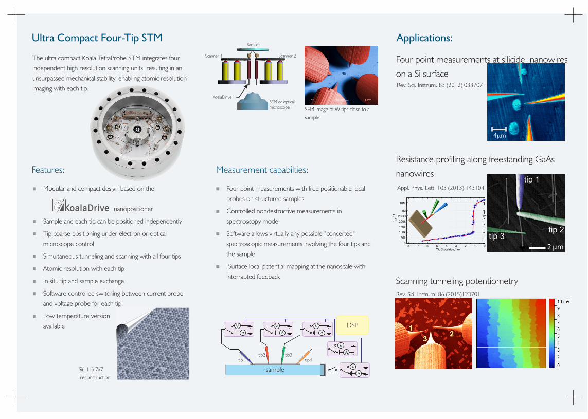
Ultra Compact Four-Tip STM
Measurement capabilties:
The ultra compact Koala TetraProbe STM integrates four
independent high resolution scanning units, resulting in an
unsurpassed mechanical stability, enabling atomic resolution
imaging with each tip.
Features:
Modular and compact design based on the
nanopositioner
Sample and each tip can be positioned independently
Tip coarse positioning under electron or optical
microscope control
Simultaneous tunneling and scanning with all four tips
Atomic resolution with each tip
In situ tip and sample exchange
Software controlled switching between current probe
and voltage probe for each tip
Low temperature version
available
Four point measurements with free positionable local
probes on structured samples
Controlled nondestructive measurements in
spectroscopy mode
Software allows virtually any possible “concerted“
spectroscopic measurements involving the four tips and
the sample
Surface local potential mapping at the nanoscale with
interrapted feedback
Si(111)-7x7
reconstruction
4m
Sample
Scanner 1 Scanner 2
KoalaDriveSEM or opticalmicroscope
Applications:
Four point measurements at silicide nanowires
on a Si surfaceRev. Sci. Instrum. 83 (2012) 033707
Resistance profiling along freestanding GaAs
nanowires
Appl. Phys. Lett. 103 (2013) 143104
2 µm
tip 1
tip 2tip 3
Scanning tunneling potentiometry
Rev. Sci. Instrum. 86 (2015)123701
SEM image of W tips close to a
sample
V
A
V
A
V
A
V
A
V
A
sample
DSP
tip1tip2 tip3
tip4