thermo-mechanical characterization of motorola mma1201p accelerometer ... · thermo-mechanical...
TRANSCRIPT

Page 1 of 19
Thermo-Mechanical Characterization of Motorola MMA1201PAccelerometer Test Report
Ashok. K. Sharma/[email protected]
Alaexander TeverovskyQSS Group, Inc./NASA
Frederick FeltQSS Group, Inc./NASA
Part Description
Motorola MMA1201P is a single-axis, surface micromachined MEMS accelerometerrated for ±40 G and is packed in a plastic 16-lead DIP package. The operatingtemperature range is –40 °C to +85 °C with a storage temperature range of –40 °C to+105 °C. The part can sustain accelerations up to 2000 g from any axis while unpoweredand powered accelerations up to 500 g.
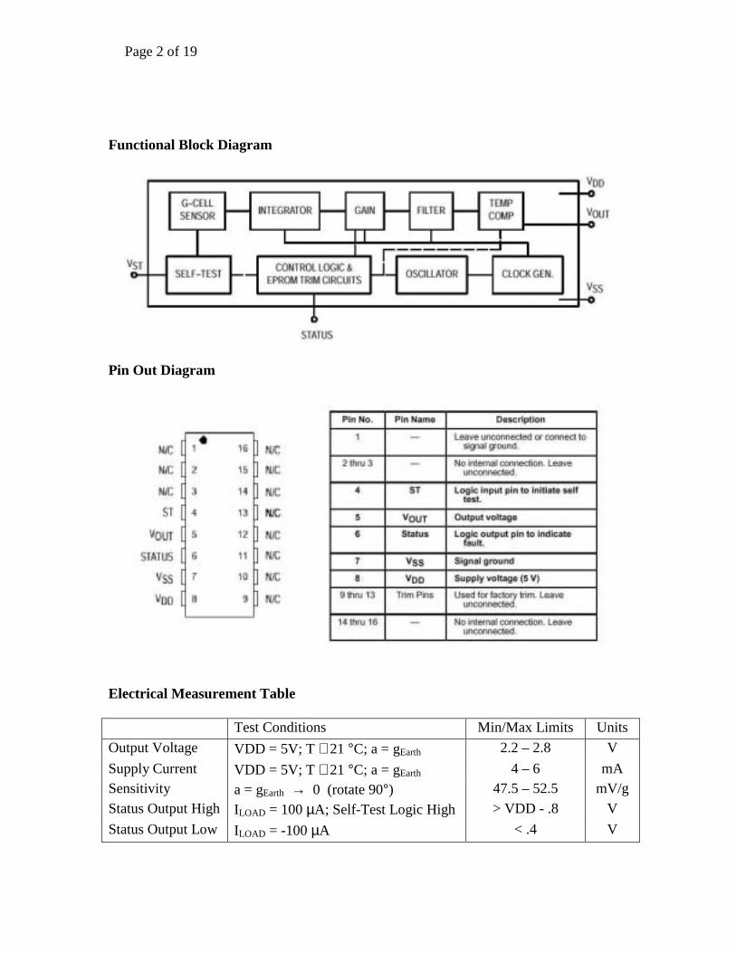
The main components of the MMA1201P consist of a surface micromachined capacitivesensing cell (g-cell) and a CMOS signal conditioning ASIC. The g-cell’s mechanicalstructure is composed of three consecutive semiconductor plates, defining sensitivityalong the Z-axis (orthogonal to flat plane of the chip). When the accelerometer system issubjected to accelerations with components parallel to the sensitive axis of the g-cell, thecenter plate moves relative to the outer stationary plates, causing two shifts incapacitance, one for each outer plate, proportional to the magnitude of force applied. Theshifts in capacitance are then processed by the CMOS ASIC, which determines theacceleration of the system (using switched capacitor techniques), conditions and filtersthe signal, and returns a ratiometric high voltage output.
A fourth semiconductor plate located in the g-cell allows testing of the accelerometermechanics and electronics. When this plate is properly biased, an electrostatic forcecauses the movable plate to displace, causing changes in capacitance that can beprocessed by the CMOS ASIC as an acceleration, returning an output voltageproportional to the test plate bias. A fault latch, which is linked to the self-test system,can deactivate the accelerometer in cases of insufficient supply voltage, clock frequency,or changes in EPROM parity to odd. A rising edge on the self-test input pin will reset thelatch.
Page 2 of 19
Functional Block Diagram
Pin Out Diagram
Electrical Measurement Table
Test Conditions Min/Max Limits UnitsOutput Voltage VDD = 5V; T ≅ 21 °C; a = gEarth 2.2 – 2.8 VSupply Current VDD = 5V; T ≅ 21 °C; a = gEarth 4 – 6 mASensitivity a = gEarth → 0 (rotate 90°) 47.5 – 52.5 mV/gStatus Output High ILOAD = 100 µA; Self-Test Logic High > VDD - .8 VStatus Output Low ILOAD = -100 µA < .4 V
Page 3 of 19
Test Plan
I. Incoming InspectionExternal examination, serialization, X-ray.
II. Thermal Cycling and Mechanical Shock1. Low Range Thermal Cycle -40 to +105 °C (25 samples)
Electrical tests after 100, 200, 500, and 1000 cumulative cycles.
2. High Range Thermal Cycle -65 to +155 °C (25 samples)Electrical tests after 30, 100, 200, 300, 500, 1000 cumulative cycles.
3. Mechanical Shocks 2000 g (20 samples)Electrical tests after 30, 130, 430, 1430, 2500, 5000, 10000 cumulative shocks
III. Failure AnalysisAll failed parts from cycling and shock tests were sent to FA for inspection.
Test Results
I. Thermal Cycling
Test results are shown in Table 1 and in Figure 1.
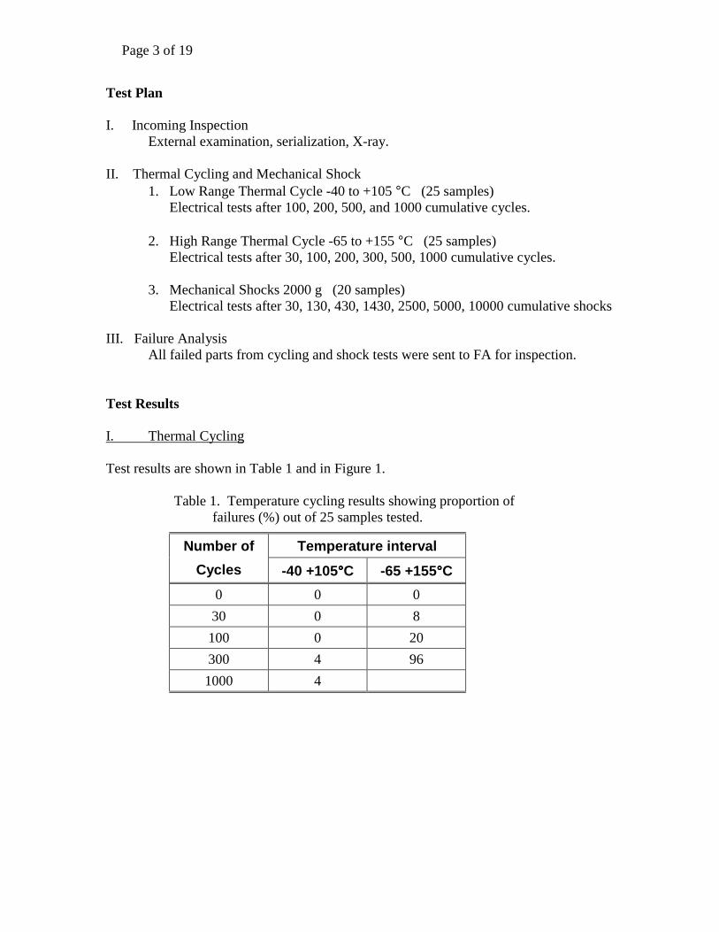
Table 1. Temperature cycling results showing proportion offailures (%) out of 25 samples tested.
Number of Temperature intervalCycles -40 +105°°°°C -65 +155°°°°C
0 0 030 0 8100 0 20300 4 961000 4

Page 4 of 19
Figure 1. Temperature cycling test results showing proportion of Failures (%) versus number of cycles
II. Mechanical shock.
Test results are shown in Table 2.
Table 2. 2000 g Mechanical Shock Results. (25 samples).
Number ofShocks
Proportion offailures, %
0 030 0
130 16430 20*
1430 202500 205000 20
10000 20
* one sample failed IDD high after 430 shocks, but then recovered after it was tappedseveral times, and showed normal IDD reading.
Summary and Conclusions
A total of 70 Motorola MEMS accelerometers were subjected to incoming inspectionconsisting of visual examination, serialization, X-Ray, Thermal Cycling within LowRange of -40 to +105°C (25 samples) and Thermal Cycling Extended Range of –65 to +155°C (25 samples). Electrical test results were performed after 100, 200, 500, and 1000cumulative cycles. Twenty parts were subjected to Mechanical Shocks (MS) of 2000 gwith electrical tests after 30, 130, 430, 1430, 2500, 5000, 10000 cumulative shocks.
MMA1201P Accelerometers. Temperature Cycling.
020406080
100120
1 10 100 1000
number of cycles
Prop
ortio
n of
fa
ilure
s, % -40 +105
-65 +155

Page 5 of 19
Test results showed no failures during low TC range testing till 100 cycles, and 4 % partsfailing post 300 – 1000 TC electrical tests. During extended range TC testing, 8 % partsfailed post 30 TC electricals and 96 % parts failed post 300 electricals. Mechanical shocktesting showed no failures till 16 MS, and 16 – 20 % failures from 130 – 10,000 MS.These parts are not recommended for use in rugged environment and space flightapplications.
The failed parts were subjected to failure analysis. Analysis indicated that temperaturecycling caused the shrinkage of the internal silicon glop surrounding the sensor, resultingin broken internal wires and accelerometer failure. The failure mechanism for the partsfailing shock testing has not been determined yet. However, the hybrid construction ofthe part suggests that multiple shocks in the z-axis might overstress the fragile siliconmembrane of the transducer. Details are provided in the failure and constructionanalysis report in attached Appendix A.
Acknowledgements
This work was supported by NASA NEPP Program and was performed as a part ofCOTS MEMS Sensors/Accelerometers Quality and Reliability Characterization testing.

Page 6 of 19
APPENDIX A
MOTOROLA MMA 1201P ACCELEROMETERS FAILUREAND CONSTRUCTION ANALYSIS REPORT

Page 7 of 19
Motorola Accelerometers (MMA1201P) Failure andConstruction Analysis Report
Background
An evaluation of plastic-encapsulated Motorola accelerometers wasconducted for NEPP program. One group of parts were exposed totemperature-cycle testing, of 30 to 100 cycles. Another group ofaccelerometers was exposed to shock testing of between 200 and 430shock events. Following these tests, electrical testing determined thatmany of the accelerometers had failed. The failing parts were forwarded tothe GSFC Failure Analysis Laboratory for determination of cause offailure.
In addition, two untested parts were provided for construction analysis.
Part Description
The MMA1201P Motorola Accelerometer is a micomachined devicefeaturing integral signal conditioning, linear output, and ratiometricperformance. The part uses a 4th order Bessel function filter to preservepulse shape. It is calibrated for self-test. The transducer is hermeticallysealed. The literature claims that the part is of a robust design, with highshock survivability. The parts are 16-pin DIPS in a plastic encapsulatedpackage. No specifications for temperature extremes or shock areprovided in the manufacturer’s data sheets.
Analysis and Results
The parts were electrically tested to confirm the failures. It was observedthat, of the parts subjected to temperature-cycling, all the failing partsfailed due to the Voff parameter reading in the millivolt range, when thecorrect reading should have been approximately 2.5 volts. Similarly, thefailing parts subjected to shock failed the VoH parameter, read in themillivolt range, where as the correct reading should have beenapproximately 5.0 volts. Therefore, the pattern of electrical failuressuggested a common failure mode for temperature-cycling, and a secondcommon, but different, failure mode for shock test.
The parts were examined externally and photo-documented. No anomalieswere found. The parts were x-rayed, revealing that the accelerometeressentially had a hybrid construction, and consisted of a microcircuit andan internal sensor/transducer. Gold bond wires connected the microcircuitto the external lead frame, while internal wires linked the microcircuit tothe sensor.
Page 8 of 19
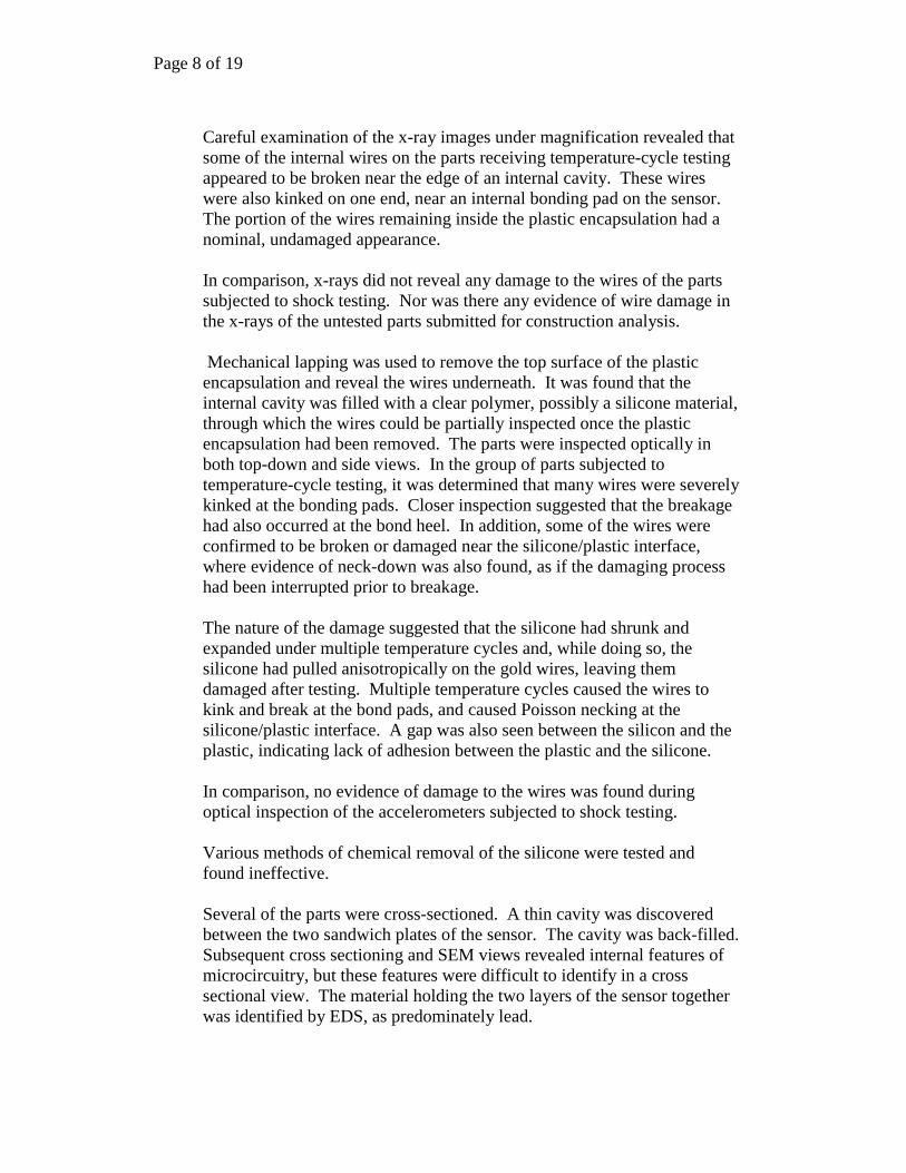
Careful examination of the x-ray images under magnification revealed thatsome of the internal wires on the parts receiving temperature-cycle testingappeared to be broken near the edge of an internal cavity. These wireswere also kinked on one end, near an internal bonding pad on the sensor.The portion of the wires remaining inside the plastic encapsulation had anominal, undamaged appearance.
In comparison, x-rays did not reveal any damage to the wires of the partssubjected to shock testing. Nor was there any evidence of wire damage inthe x-rays of the untested parts submitted for construction analysis.
Mechanical lapping was used to remove the top surface of the plasticencapsulation and reveal the wires underneath. It was found that theinternal cavity was filled with a clear polymer, possibly a silicone material,through which the wires could be partially inspected once the plasticencapsulation had been removed. The parts were inspected optically inboth top-down and side views. In the group of parts subjected totemperature-cycle testing, it was determined that many wires were severelykinked at the bonding pads. Closer inspection suggested that the breakagehad also occurred at the bond heel. In addition, some of the wires wereconfirmed to be broken or damaged near the silicone/plastic interface,where evidence of neck-down was also found, as if the damaging processhad been interrupted prior to breakage.
The nature of the damage suggested that the silicone had shrunk andexpanded under multiple temperature cycles and, while doing so, thesilicone had pulled anisotropically on the gold wires, leaving themdamaged after testing. Multiple temperature cycles caused the wires tokink and break at the bond pads, and caused Poisson necking at thesilicone/plastic interface. A gap was also seen between the silicon and theplastic, indicating lack of adhesion between the plastic and the silicone.
In comparison, no evidence of damage to the wires was found duringoptical inspection of the accelerometers subjected to shock testing.
Various methods of chemical removal of the silicone were tested andfound ineffective.
Several of the parts were cross-sectioned. A thin cavity was discoveredbetween the two sandwich plates of the sensor. The cavity was back-filled.Subsequent cross sectioning and SEM views revealed internal features ofmicrocircuitry, but these features were difficult to identify in a crosssectional view. The material holding the two layers of the sensor togetherwas identified by EDS, as predominately lead.

Page 9 of 19
A sensor was extracted from its encapsulating silicone and photo-documented. Its construction suggested that the sensor had been glued tothe lead frame, then encapsulated under a silicone drop, and then the wholepart, including lead frame and microcircuit, was subjected to plasticencapsulation.
One of the sensors was selected for destructive deprocessing. Afterremoval of the glue and silicone, the sensor was attached to a metal wandand carefully split open using a microscope and a razor.
Internal SEM and EDS inspection revealed that the accelerometer sensorconsists of a silicon membrane supported at four corners. This membranestands above another silicon layer on the substrate. The sensor apparentlyworks because of capacitance changes as the membrane deflects underacceleration. The lid of the cavity appears to form one plate of thecapacitor. Also the substrate may form another plate. Four serpentineresistors and pads were observed on the substrate near the center of thetransducer. A long integration EDS of the membrane indicated virtuallypure silicon with a trace of cobalt.
While the cause of failure for the shock-tested parts has not yet beendetermined, it is suspected that shock in the z-axis direction may havecaused damage to the unsupported silicon membrane.
Failure Analysis Conclusions
Temperature-cycle testing caused the shrinkage of the internal siliconeglop surrounding the sensor, resulting in broken internal wires andaccelerometer failure
The cause of failure of the parts damaged during shock-testing has not yetbeen determined. However, the construction of the part suggests thatmultiple shocks in the z-axis might have overstress the fragile siliconmembrane of the transducer.

Page 10 of 19
Figure 1. An external top view of theaccelerometer manufactured by Motorola. 5X
Figure 2. An external bottom view of the acceler-ometer. 5X

Page 11 of 19
Figure 3. X-ray view of accelerometer revealsthat it is a hybrid device. A large microcircuit atleft is wire-bonded to the lead-frame. Internalwires bridge to the sensor. Arrow indicatesdefect seen better in Figure 4. 10X
Figure 4. Close examination of the bridging wiresinside the part reveals an apparent break in the topwire in this photo. The large, faint shadow overthe sensor indicates the cavity filled with silicone.Note that wire break occurs near the interface ofthe plastic and the silicone. SN76 failed undertemperature-cycle testing. 25X

Page 12 of 19
Figure 5. A similar, but more severe problemwas noted on SN78, which also underwenttemperature-cycle testing. Many of the abovewires are broken. All of the wires appear wavy orkinked on the right. 25X
Figure 6. A second group of accelerometers faileddue to shock. This representative device x-rayshows no evidence of wire breakage or kinking.25X
Figure 7. The bridging wires are seen in sideview in this x-ray of SN78. Most of the wiresbroke at a common location near the edge of thecavity. Note that on the left of the break the wireis smooth; on the right it is kinked. 25X
Figure 8. SN264 failed due to shock. Notice thatthe wires are not damaged. The arrow on the leftpoints to an enhanced region showing the leaddress of the wires bonded between the lead frameand the microcircuit. Arrow on the right indicateswhere the wires attach to the top of the sensor,which cannot be seen in this x-ray. 25X
Page 13 of 19
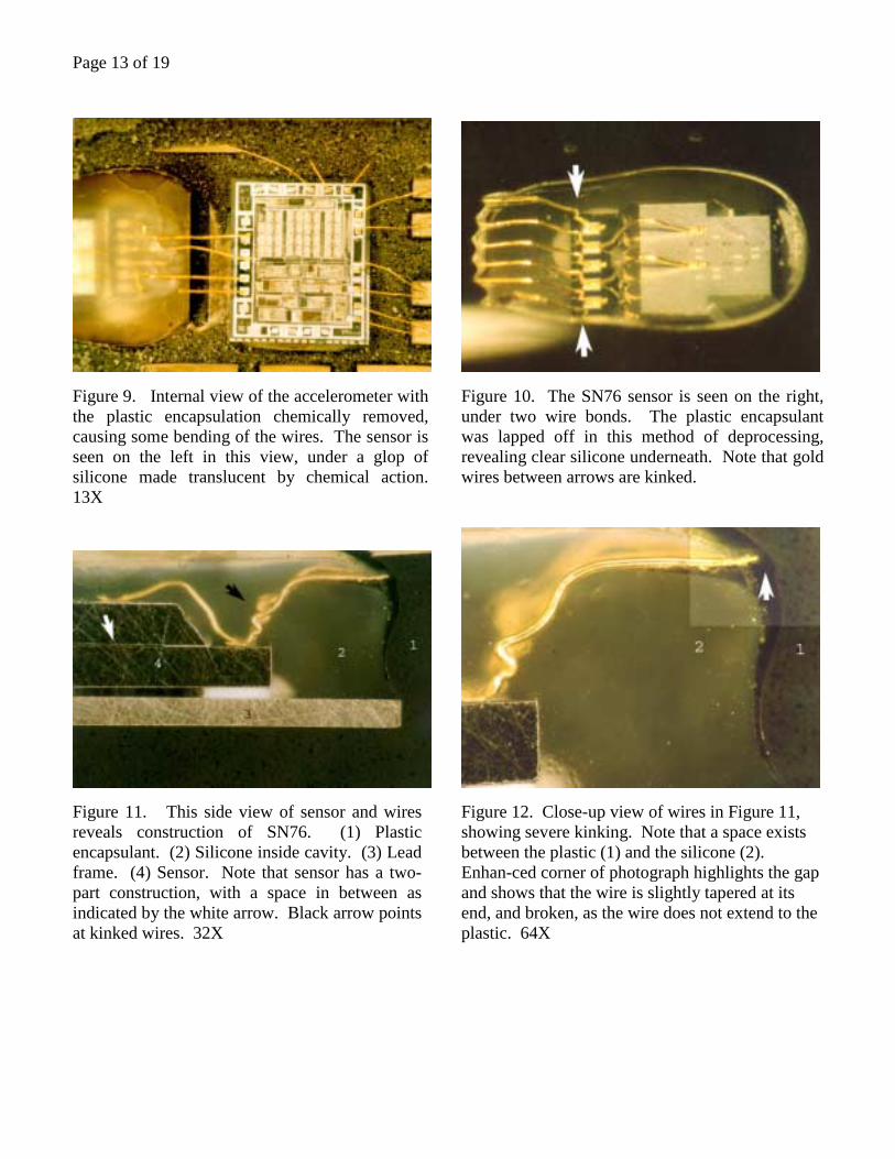
Figure 9. Internal view of the accelerometer withthe plastic encapsulation chemically removed,causing some bending of the wires. The sensor isseen on the left in this view, under a glop ofsilicone made translucent by chemical action.13X
Figure 10. The SN76 sensor is seen on the right,under two wire bonds. The plastic encapsulantwas lapped off in this method of deprocessing,revealing clear silicone underneath. Note that goldwires between arrows are kinked.
Figure 11. This side view of sensor and wiresreveals construction of SN76. (1) Plasticencapsulant. (2) Silicone inside cavity. (3) Leadframe. (4) Sensor. Note that sensor has a two-part construction, with a space in between asindicated by the white arrow. Black arrow pointsat kinked wires. 32X
Figure 12. Close-up view of wires in Figure 11,showing severe kinking. Note that a space existsbetween the plastic (1) and the silicone (2).Enhan-ced corner of photograph highlights the gapand shows that the wire is slightly tapered at itsend, and broken, as the wire does not extend to theplastic. 64X

Page 14 of 19
Figure 13. The gap between the plastic (1) andsilicone (2) is seen in this view of SN77. Arrowpoints to a wire region inside the gap whichexhibits necking. 64X
Figure 14. Another view of a part which did notexperience temperature-cycling. SN262 failedshock testing. Observe that the wires arecontinuous and smooth, with no evidence ofbreakage or kinking. 16X
Figure 15. A side view of SN262 indicates thewires are in excellent condition, unlike the partsthat experienced temperature-cycle testing. 16X
Figure 16. SN281 was submitted for constructionanalysis. Note that the wires of the device, asmanufactured, appear unbroken and smooth. 16X

Page 15 of 19
Figure 17. Inverted view of sensor (3), showingthe silicone (1), and four white, apparentlypolymer glue feet (2). 16X
Figure 18. Black arrow indicates silicon substratein this view of the sensor after destructive opening.White arrow indicates the actual accelerometer.(1) Cavity. (2) Lead bonding material. (3) Bondpads. 32X
Figure 19. Optical view of accelerometer sensorinside cavity. 64X
Figure 20. The lid of the sensor is shown on right.Note that an electrical trace appears to connectwith the dark surface, which is presumablyconductive. 32X
Page 16 of 19
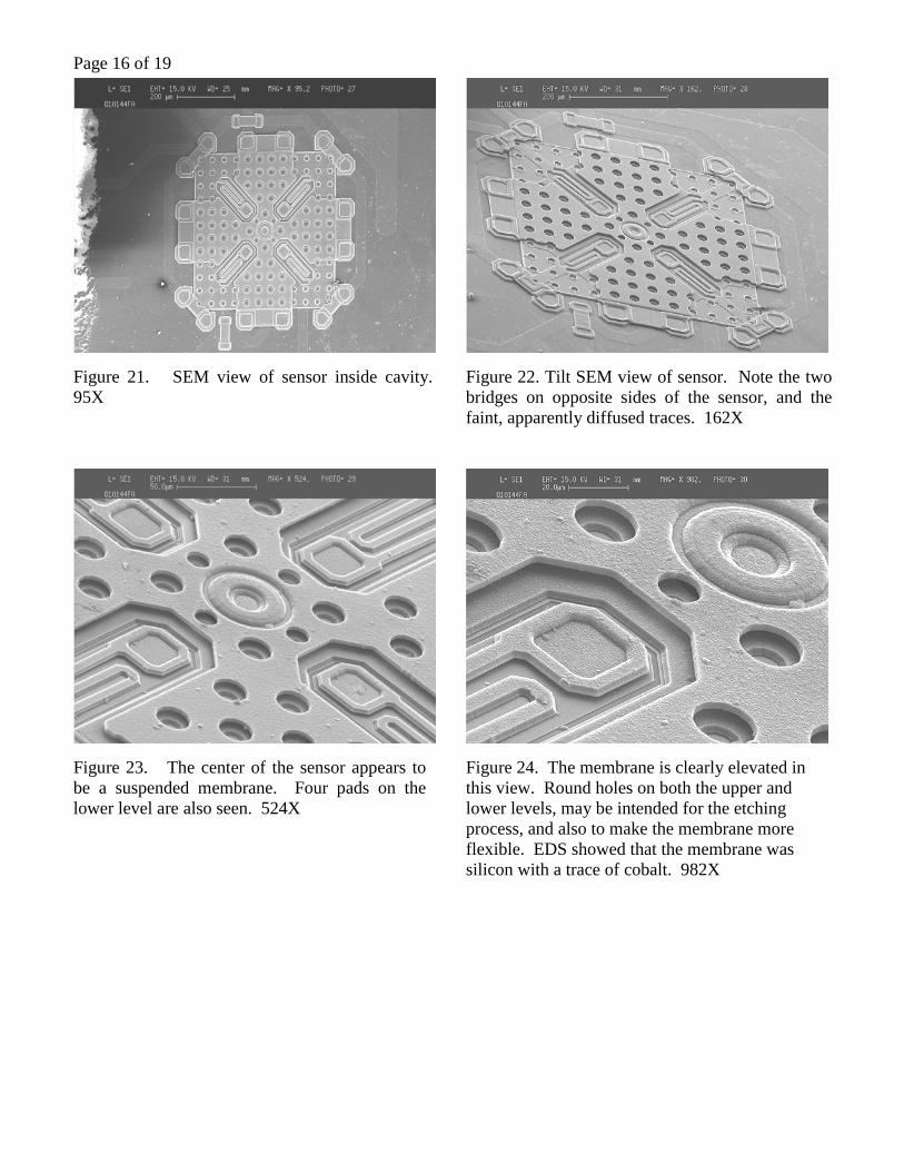
Figure 21. SEM view of sensor inside cavity.95X
Figure 22. Tilt SEM view of sensor. Note the twobridges on opposite sides of the sensor, and thefaint, apparently diffused traces. 162X
Figure 23. The center of the sensor appears tobe a suspended membrane. Four pads on thelower level are also seen. 524X
Figure 24. The membrane is clearly elevated inthis view. Round holes on both the upper andlower levels, may be intended for the etchingprocess, and also to make the membrane moreflexible. EDS showed that the membrane wassilicon with a trace of cobalt. 982X

Page 17 of 19
Figure 25. A corner view of the sensor. EDSindicated that the lower level was also composedof silicon. Serpentine path appears to be a resistorconnecting to a pad. 351X
Figure 26. Close-up of the pad. The membraneappears suspended in this high-angle view. 1560X
Figure 27. Note that the lower level of siliconappears to be elevated at the left end, behind theresistor, while also being down at the right side,creating a gentle slope. It is not understood ifthis is an artifact of the manufacturer’s etchingprocess, or necessary for the device operation.1100X
Figure 28. Close-up of resistor. An edge of themembrane is in the foreground. Note the slope onthe resistor, while the pad, itself is intimate withthe substrate. 1500X
Page 18 of 19
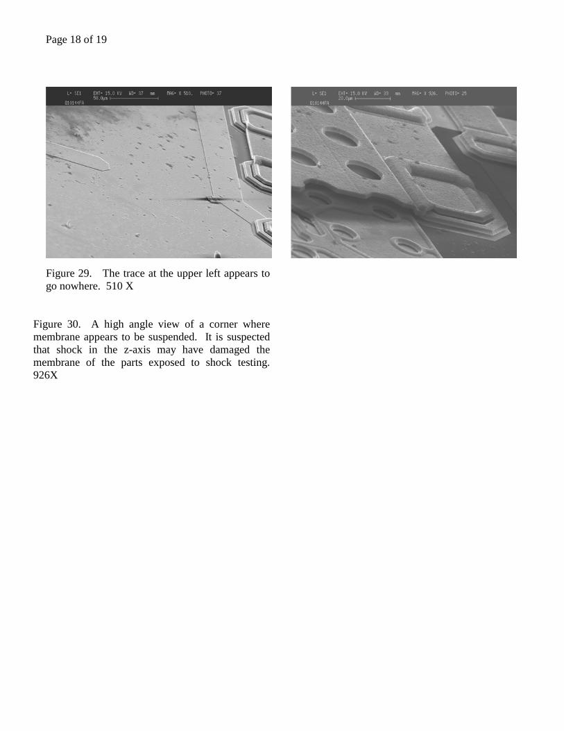
Figure 29. The trace at the upper left appears togo nowhere. 510 X
Figure 30. A high angle view of a corner wheremembrane appears to be suspended. It is suspectedthat shock in the z-axis may have damaged themembrane of the parts exposed to shock testing.926X

Page 19 of 19 19
Figure 31. Motorola logo. 347X