theory and practical considerations of multilayer...
TRANSCRIPT

Theory and practical considerations ofmultilayer dielectric thin-film stacksin Ag-coated hollow waveguides
Carlos M. Bledt,1,2,* Jeffrey E. Melzer,1 and James A. Harrington1
1School of Engineering, Rutgers University, 607 Taylor Road, Piscataway, New Jersey 08854, USA2School of Engineering, Brown University, 182 Hope Street, Providence, Rhode Island 02912, USA
*Corresponding author: [email protected]
Received 30 August 2013; accepted 7 October 2013;posted 11 October 2013 (Doc. ID 196758); published 15 November 2013
This analysis explores the theory and design of dielectric multilayer reflection-enhancing thin film stacksbased on high and low refractive index alternating layers of cadmium sulfide (CdS) and lead sulfide (PbS)on silver (Ag)-coated hollow glass waveguides (HGWs) for low loss transmission at midinfrared wave-lengths. The fundamentals for determining propagation losses in such multilayer thin-film-coated Aghollowwaveguides is thoroughly discussed, and forms the basis for further theoretical analysis presentedin this study. The effects on propagation loss resulting from several key parameters of these multilayerthin film stacks is further explored in order to bridge the gap between results predicted through calcu-lation under ideal conditions and deviations from such ideal models that often arise in practice. In par-ticular, the effects on loss due to the number of dielectric thin film layers deposited, deviation from idealindividual layer thicknesses, and surface roughness related scattering losses are presented and thor-oughly investigated. Through such extensive theoretical analysis the level of understanding of the under-lying loss mechanisms of multilayer thin-film Ag-coated HGWs is greatly advanced, considerablyincreasing the potential practical development of next-generation ultralow-loss mid-IR Ag/multilayerdielectric-coated HGWs. © 2013 Optical Society of AmericaOCIS codes: (310.4165) Multilayer design; (310.6805) Theory and design; (060.2390) Fiber optics,
infrared; (310.1620) Interference coatings; (080.1753) Computation methods.http://dx.doi.org/10.1364/AO.53.000A70
1. Introduction
Hollow glass waveguides (HGWs) have been widelyused in a variety of applications requiring the low-losstransmission of infrared radiation, ranging fromhigh-powered medical laser delivery to broadbandspectroscopic chemical gas sensing. In contrast toother current types of infrared waveguides and opti-cal fibers,HGWshave a variety of advantages, includ-ing no end reflection, chemical and mechanicalstability, high throughput power thresholds, broad-band transmission, and easily tunable optical
response to meet the requirements of a particular ap-plication. HGWs consist of a fused silica capillary,usually of constant bore radius,a,whose inner surfaceis coated with a uniform reflective silver (Ag) film ap-proximately 200 nm thick, followed by a dielectricthin film of adequate thickness, depending on the de-sired optical response [1,2]. This dielectric thin-filmenhances the reflectivity, thus lowering the propaga-tion loss of the waveguide through constructive inter-ference effects. Commonly deposited dielectric thinfilm materials in HGWs include silver iodide (AgI),cadmium sulfide (CdS), lead sulfide (PbS), and morerecently polymers such as polystyrene (PS) [1,3].
As will be discussed in further detail in the pro-ceeding section, the propagation loss of hollow
1559-128X/14/040A70-13$15.00/0© 2014 Optical Society of America
A70 APPLIED OPTICS / Vol. 53, No. 4 / 1 February 2014

waveguides (HWs) depends directly on the wave-guide bore size, the angle of propagation of theguided ray, and the reflectance of the inner wave-guide surface. Of these loss-determining parameters,both the waveguide bore and the propagation angleare largely fixed by the target application and, assuch, cannot be altered to decrease the overall propa-gation loss. This then leaves the inner surface reflec-tance as the only practical tunable parameter inreducing HW losses. As previously mentioned,HGWs have traditionally made use of only a singlereflection-enhancing dielectric film, yet the use ofa single dielectric thin film can only reduce thepropagation loss so much, depending on the refrac-tive index of the dielectric thin film material used,the quality of the deposited dielectric and Ag films,and of course the thickness of the dielectric thin film.Even when considering perfect film quality and opti-mal film thickness, the maximum achievable loss re-duction when using a single dielectric thin film islimited and has been calculated to occur when therefractive index of the dielectric material is 1.414[1,4]. To further reduce propagation losses in HWsin hopes of developing next-generation ultralow-lossHGWs, it is therefore necessary to pursue an in-crease in waveguide surface reflectance through analternative method.
Of the limited possibilities in achieving such adesired substantial increase in reflectance, themost obvious and practical is the incorporation ofreflection-enhancing low and high refractive indexalternating thin film stacks in lieu of a singledielectric thin film, thus having the potential oftremendously increasing the reflectivity [1,4–10].Figure 1 gives a representation of such a proposedAg/multilayer dielectric stack HGW structure, alongwith a representative radial refractive index profile ofthe functional film materials in the proposed struc-ture for both an even and odd number of layers com-posing themultilayer dielectric structure. It should benoted that the reflectance is most enhanced for anygiven total number of layers, N, when the film adja-cent to the Ag film is composed of the low indexmaterial and, as such, the proceeding analysis will
consistently incorporate this. Furthermore, the thick-ness of the innermost (surface) layer must differ fromthose layers composed of the same material withinthe multilayer structure and will depend on the totalnumber of layers and whether an odd or even totalnumber of layers are incorporated in the structure,as will be discussed in further detail [1,4,10].
By introducing multilayer dielectric stack struc-tures to enhance the reflectivity of HGWs, the reflec-tance can be considerably increased, particularly asthe number of total alternating low and high indexlayers increases and as the refractive index mis-match of the constituent layer materials increases.Of the commonly deposited dielectric film materials,CdS (nCdS ! nL ≈ 2.25) and PbS (nPbS ! nH ≈ 4.25)pose as excellent candidates for the development ofsuch multilayer stacks, due to their high IR trans-parency, well-developed deposition procedures,chemical compatibility and. above all, their high in-dex mismatch (nPbS∕nCdS ! nH∕nL ≈ 1.85) [1,11,12].As such, this study will focus exclusively on theuse of these two materials in HGWs for the theoreti-cal analysis of said proposed multilayer structures.The proceeding analysis will extend past the pointof ideal Ag/multilayer coatings in HGWs to explorethe effects of challenges often seen in practice, par-ticularly due to film thickness variability and theintroduction of scattering loss due to inevitablesurface roughness.
2. Calculation of Waveguide Propagation Losses
Propagation loss in HWs can be theoretically deter-mined via several methods, involving, most com-monly, either a wave or ray-optics approachdepending on the type of analysis desired. Whilethe wave-optics approach, thoroughly developed byMiyagi and Kawakami [4], is most suitable for directdetermination of propagation losses for specificpropagating modes, it inherently assumes that alldielectric thin-film(s) are of optimal thickness forthe wavelength of light used in the calculation. Assuch, this model is most appropriate for determiningpropagation loss as a function of propagatingmode ata specific target wavelength, rather than for deter-mining the broadband spectral response of the wave-guide for which the thickness of the individuallayer(s) may or may not be optimized dependingon the wavelength of light. In contrast, through theray-optics approach previously analyzed by Miyagi[13] and Matsuura et al. [14], the waveguide losscan be determined as a function of wavelength withfreedom in the variability of the thickness of the indi-vidual layer(s) in the dielectric waveguide structure.Through this approach, the treatment of propagatinglight rays at any propagation angle is inherent and,as such, lends itself to much simpler analysis ofpropagation losses in more unconventional wave-guide configurations than the wave-optics approach,such as in waveguides subjected to an applied exter-nal curvature and/or tapered bore HWs in which thepropagation angle may be dynamic in nature. Most
Fig. 1. (a) Cross-sectional representation of Ag/multilayer dielec-tric stack-coated HGW and (b) representative refractive indexprofile of functional HGW thin films.
1 February 2014 / Vol. 53, No. 4 / APPLIED OPTICS A71

importantly for the present analysis, however, theray-optics approach to determining HW attenuationdepends directly on the reflectivity of the inner HWsurface due to the Ag/multilayer structure and, assuch, the reflectivity can be found as a function ofthe structure in question and then used to determinethe waveguide loss.
A. Ray-Optics Calculation of Waveguide Loss
In determining the waveguide loss through ray-optics analysis, the focus will be placed exclusivelyon meridional light rays propagating along a straightHW of constant bore size. While skew rays maypropagate short distances along the waveguidelength, their contribution to the total waveguide lossis much smaller than that of meridional rays andcan be considered negligible for waveguides oflengths appreciable for any practical applications[1,4,13,14]. In considering a propagating meridionalray along a HW of bore radius a, with propagationangle φ with respect to the optic axis, as presentedin Fig. 2, it can be seen that its loss depends onthe reflectivity of the inner waveguide surface ateach successive reflection. From trigonometric analy-sis, for a ray of constant propagation angle, the dis-tance between each successive reflection, L, is givenby Eq. (1) [1,13,14],
L !2a
tan φ! 2a cot φ: (1)
The length between successive reflections thus de-pends on the bore size and the propagation angle, in-creasing with decreasing propagation angle andincreasing bore size. The additional ray displace-ment along the optic axis due to the Goos–Hänchenshift at each reflection is very small relative to thelength between each successive reflection has negli-gible contribution in the calculation and is thus omit-ted [15,16]. The number of reflections per unit lengthis then inversely proportional to this quantity, withthe power attenuation coefficient, 2α, being equal tothe number of reflections per unit length times theabsorption loss of the inner HW surface structure.This then gives the HW attenuation per unit lengthin units of dB/m as a function of propagation angle,bore size, and inner surface reflectance as [13,14]
2α ! 10 ·A
2a cot φ→ α ! 10 ·
1 − R"φ#4a cot φ
; (2)
where the inner surface reflectance, R, is itself afunction of propagation angle and several otherquantities to be subsequently discussed. Using thisray-optics method for determining the loss ofmeridional rays in HWs, the modeling versatility forthe pursuing analysis of multilayer dielectric thinfilm stacks in Ag-coated HGWs is inherent and isthus adopted as the foundation for this study.
B. Reflectance Calculation via Transfer Matrix Method
The task then becomes calculating the reflection co-efficient of an Ag/multilayer dielectric stack struc-ture as a function of wavelength, layer materialsand thicknesses, and incident angle, θ ! 90 − φ. Ofthe several mathematical methods in determiningthe reflectivity of such an Ag/multilayer dielectricstack-coated HGW structure, perhaps the mostversatile and convenient, and that used in this study,is the transfer matrix method. The transfer matrixmethod inherently allows for the determination ofthe reflection coefficient for a multilayer structurewith N finite number of thin films by relating thebackward and forward propagating field amplitudesacross each layer [5,7,8]. For an interface, this isachieved with a matching matrix characteristic tothe particular interface and, for propagation througheach layer, this is achieved with a propagation ma-trix characteristic to the particular layer material.Eq. (3) defines the characteristic transfer matrix,$Ti%, for the propagation of a light ray at an interfacebetween the ith − 1 and ith layers and subsequentpropagation through the ith layer [5],
$Ti% !1
τi−1;i
!1 ρi−1;i
ρi−1;i 1
"!ejkidi 00 e−jkidi
"; (3)
where ki is the wavenumber of light in the ith layer,di is the thickness of the ith layer, and τi−1;1 and ρi−1;1,are the transverse Fresnel transmission and reflec-tion coefficients, respectively, between the ith − 1and ith layers, defined for s and p polarized lightby Eqs. (5) as follows [5,8]:
ρsi−1;i !
ηicos"θi#
−ηi−1
cos"θi−1#ηi
cos"θi#&
ηi−1cos"θi−1#
; (4a)
τsi−1;i !2
ηicos"θi#
ηicos"θi#
&ηi−1
cos"θi−1#
; (4b)
ρpi−1;i !ηi cos"θi# − ηi−1 cos"θi−1#ηi cos"θi# & ηi−1 cos"θi−1#
; (4c)
τpi−1;i !2ηi cos"θi#
ηi cos"θi# & ηi−1 cos"θi−1#; (4d)Fig. 2. Geometrical representation of meridional ray propagating
along a section of a HW (not to scale).
A72 APPLIED OPTICS / Vol. 53, No. 4 / 1 February 2014

where ηi and ηi−1 are the impedances of the ith andith − 1 layer materials, respectively. The characteris-tic matrix for the entire multilayer dielectric filmstack, $TN % is then the product of the characteristicmatrices for each interface matching/layer propaga-tion characteristic matrices $Ti% up toN total numberof layers
$TN % !YN
i!1
$Ti%; (5)
where it should be noted that the “zeroth” layer is theinitial medium of incidence or, in this case, freespace. Furthermore, to account for the reflection ofthe interface between the dielectric layer closest tothe Ag film and the Ag film, $TN % is multipliedby the matching matrix for this interface to yieldthe characteristic matrix of the entire Ag/multilayerstructure system, $T%
$T% ! $TN %1
τN;Ag
!1 ρN;Ag
ρN;Ag 1
": (6)
Considering that the amplitude of the incident lighton the system is unity (E&
0 ! 1), and there is no back-ward propagating wave from the Ag film (E−
Ag ! 0),the reflection coefficient of the system is then deter-mined from this characteristic product matrix for theentire system as in Eq. (9) [5,8]
!E&
0E−
0
"! $T%
!E&
AgE−
Ag
"→
!1E−
0
"!
!T11 T12T21 T22
"!E&
Ag0
";
(7a)
#1 ! E&
AgT11
E−0 ! E&
AgT21→
#E&Ag !
1T11
E−0 ! T21
T11
→ r !E−
0
E&0!
T21
T11;
(7b)
R ! jrr'j !$$$$
%T21
T11
&·%T21
T11
&'$$$$: (7c)
This calculation is carried out for both s and p polar-ized light in order to obtain the total reflection of thesystem, and hence the inner surface of the HW. Thisreflection coefficient is used in conjunction withEq. (2) to determine the propagation loss of an Ag/multilayer-coated HGW having a total of N reflec-tion-enhancing alternating dielectric thin films. Thismethodology was used throughout this study to de-termine the spectral optical loss of the various multi-layer structures analyzed in this study. An iterativeapproach was used in MATLAB to determine attenu-ation for a given structure as a function of wave-length and angle of propagation.
3. Fundamentals of Reducing Loss viaMultilayer Structures
In exploring reflection-enhancing multilayer dielec-tric thin film stacks, focus will first be placedon the effect of the total number of layers on theoverall waveguide loss. For all calculations inthis study, with the exception of the forthcominganalysis of waveguide loss as a function of boresize, a constant waveguide bore size of a !350 μm (ID ! 2a ! 700 μm) will be assumed, as thisbore size is often used for the majority of practicalHGW applications. Furthermore, as mentioned inthe introduction, the dielectric thin film materialsconsidered will remain constant throughout withCdS being used as the low index material and PbSas the high index material, with the film adjacentto the silver film composed of the low index material(CdS) [1,11]. These dielectric materials will be as-sumed to be lossless in the λ ! 1–12 μm region of in-terest, an assumption which is largely valid exceptfor PbS close to λ ! 1.0 μm. For optimal accuracyin the models presented, the refractive index of thedielectric film materials, as well as the Ag film, willdepend on wavelength per the dispersion data forthese materials reported by Palik [17]. Finally, anygiven layer will be assumed to be completely uni-form, such that film thickness variation does notvary as a function of position along the waveguidelength.
A. Calculating Optimal Film Thicknesses
The individual dielectric thin film thickness will de-pend on the target wavelength(s), with the optimalthickness for all but the innermost (surface) layerfor constructive interference being given by [1,4]
dF !λ0
4''''''''''''''n2F − 1
q ; (8)
where λ0 is the target wavelength of minimal propa-gation loss and nF is the refractive index of the dielec-tric material constituting that particular layer at λ0.The optimal film thickness for the innermost layer(CdS) depends on whether the total number of layers,N, amounts to an odd or even number, with Miyagideriving that for an odd number of layers thisthickness should be [4]
δL !λ0
2π''''''''''''''n2L − 1
q tan−1
×
0
@ nL
"n2L − 1#14
%nL
nH
&(N−12
)%n2L − 1
n2H − 1
&−(N−14
)1
A; (9)
where nL is the refractive index of the low indexmaterial which composes this innermost layer, andnH is the refractive index of the high index material.Conversely, in the case of a total number of even
1 February 2014 / Vol. 53, No. 4 / APPLIED OPTICS A73

dielectric layers, the optimal thickness of theinnermost film (PbS) should be [4]
δH !λ0
2π'''''''''''''''n2H − 1
q tan−1
×
0
@
''''''''''''''n2L − 1
q
nL"n2H − 1#14
%nH
nL
&(N2
)%n2L − 1
n2H − 1
&(N4
)1
A; (10)
where the innermost layer is composed of the highindex material. As previously mentioned, to achievethe largest possible increase in reflection for anygiven number of layers, the layer adjacent to theAg film should be composed of the low indexmaterial. In exploring the effect of total layers depos-ited on loss, it will be assumed that all layers are ofoptimal thickness for the target wavelength and thestructure consists of perfectly smooth interfaces.
B. Waveguide Loss as a Function of Total DielectricLayers
Considering an Ag/multilayer-coated HGW consist-ing of alternating CdS/PbS layers optimized forλ0 ! 2.94 μm, yielding dCdS ! 359 nm (nCdS ! 2.28)and dPbS ! 172 nm (nPbS ! 4.39), and guided rayswith a propagation angle of θ ! 1.0°. This specificwavelength has been chosen for analysis due to itbeing the emission wavelength of Er:YAG lasers,which have important applications and for which a
limited number of IR fibers and waveguides withvarying propagation losses are currently available.Figure 3 gives the calculated spectral response inthe near and mid-IR for N ! 2, 5, 8, and 11 alternat-ing CdS/PbS layers with CdS being adjacent to theAg film. Attenuation has been plotted using a loga-rithmic scale for optimal analysis of loss as a functionof increasing number of multilayer dielectric stacklayers at λ0 ! 2.94 μm. From the spectra presentedin Fig. 3, the characteristic shift of thin film interfer-ence peaks to longer wavelengths as the number oflayers increases is clearly evident. Furthermore, itcan be seen that through the incorporation of addi-tional layers of optimal thicknesses for the designwavelength of λ0 ! 2.94 μm, the waveguide propaga-tion loss drops dramatically as N increases. As thenumber of layers increases, the loss centered aboutthe design wavelength continues to drop, yieldingthe expected photonic bandgap response due to suchan ideal 1D multilayered dielectric structure [5,6,8].Figure 4 gives the maximum achievable loss as afunction of total number of dielectric layers for thisproposed Ag/multilayer dielectric-coated HGW, ob-tainable only when all films are of perfect qualityand of exactly the optimal thickness for maximumreflection enhancement at the design wavelengthof λ0 ! 2.94 μm. From Fig. 4 it is seen that, withthe addition of just 4 PbS/CdS alternating layers,the loss decreases by more than an order of magni-tude than that attainable using a single CdS filmfrom ∼0.44 dB∕m to ∼0.037 dB∕m. The addition of
Fig. 3. Theoretical waveguide propagation loss in the near and mid-IR for a total of (a) N ! 2, (b) N ! 5, (c) N ! 8, and (d) N ! 11 CdS/PbS alternating layers on an Ag-coated HGW of ID ! 700 μm assuming an ideal film structure optimized for λ ! 2.94 μm.
A74 APPLIED OPTICS / Vol. 53, No. 4 / 1 February 2014

10 more PbS/CdS alternating layers yields an overalldrop in attenuation of just over three orders of mag-nitude in comparison to a single CdS layer from∼0.44 dB∕m to ∼9.10 × 10⁻⁵ dB∕m. Theoretically,the reflection enhancement due to the addition ofeven just a couple of high index mismatch alternat-ing dielectric layers is very pronounced and poses alucrative mechanism for greatly reducing propaga-tion losses in HGWs.
C. Waveguide Loss as a Function of Propagation Angle
In practice, it is important to determine loss as afunction of propagation angle, which can indirectlypredict the loss for the corresponding mode of propa-gation. In metal/dielectric-coated HGWs, the lowestloss modes have been theoretically and experimen-tally shown to be hybrid modes, rather than pureTE or TM modes [4]. For a HW of given bore size,the corresponding propagation angle for a givenpropagating mode of a specific wavelength isapproximated by Eq. (11) [13],
θnm ! sin−1
%unmλ2πa
&; (11)
where unm is the mode parameter of the n, mthhybrid mode, which is the mth root of the "n − 1#thorder Bessel function [1,4,10]. The lower the propa-gation angle, (thus the lower the order of the hybridmode) the lower the propagation loss will be and themore efficient the coupling from free space to aguided ray will be. The angle of propagation of φ !1.0° corresponds to the lowest order modes and isa coupling angle commonly achieved in practice formost applications and has thus been chosen as thestandard for theoretical analysis throughout thiswork [1,13]. However, it is also important to deter-mine attenuation as a function of propagation angle,both since it may deviate depending on various cou-pling conditions and as it may change as it propa-gates along the waveguide. While for straightguides, such as is assumed in this study, the propa-gation angle can be assumed constant, this is not the
case for tapered bore waveguides and waveguidessubjected to applied external bending [1,18]. As such,determining loss as a function of propagation angle isimportant in predicting losses under such conditions.Considering a 700 μm ID Ag/multilayer dielectric-coated HW having a total number of N ! 2, 5, 8,and 11 alternating CdS/PbS layers, each of optimalthickness for λ ! 2.94 μm, attenuation as a functionof propagation angle assuming no surface roughnessat this design wavelength is presented in Fig. 5.As expected from previous analysis, the overall lossas a function of total layers decreases as the numberof layers increases. Furthermore, as suggested fromthe previous ray-optics analysis and the precedingdiscussion, it is seen that propagation losses areindeed lowest for near-grazing incidence (corre-sponding to lower order modes), and sharply in-creases as the propagation angle increases forpractical angles of propagation seen in HGWs(θ ≈ 89.9 − 85.0°). Past these angles, loss is furtherseen to increase as a function of propagation anglehaving an approximately cubic relationship. Impor-tantly, Fig. 5 shows that omnidirectional reflectivebehavior is not achievable using such an Ag/multi-layer dielectric structure as has been shown for other1D multilayer dielectric thin film stack systems.This is, furthermore, supported by the fact that de-spite giving rise to a photonic bandgap, this multi-layer system does not meet the criteria requiredfor omnidirectional reflection derived from bandtheory [5,6,19].
D. Waveguide Loss as a Function of Bore Size
For complete analysis, a brief discussion on wave-guide propagation loss as a function of waveguidebore size has been included. Considering HWs ofvarying bore sizes of 2a ! 300, 500, 700, and1000 μm, with individual dielectric layer thicknessesoptimized as previously for λ0 ! 2.94 μm and apropagating ray angle of φ ! 1.0°, the losses for thesevarious bore sizes with increasing number of totaldielectric layers is determined. These waveguidebore sizes have been particularly selected foranalysis as they represent those most commonlyemployed in HGWs for use at near and mid-IR
Fig. 4. Theoretical waveguide propagation loss at λ ! 2.94 μm asa function of total CdS/PbS alternating dielectric layers on anAg-coated HGW of ID ! 700 μm assuming an ideal film structurewith each film thickness optimized for this wavelength.
Fig. 5. Theoretical waveguide propagation loss at λ ! 2.94 μm asa function of propagation angle on an Ag-coated HGW forN ! 2, 5,8, and 11 total dielectric layers.
1 February 2014 / Vol. 53, No. 4 / APPLIED OPTICS A75
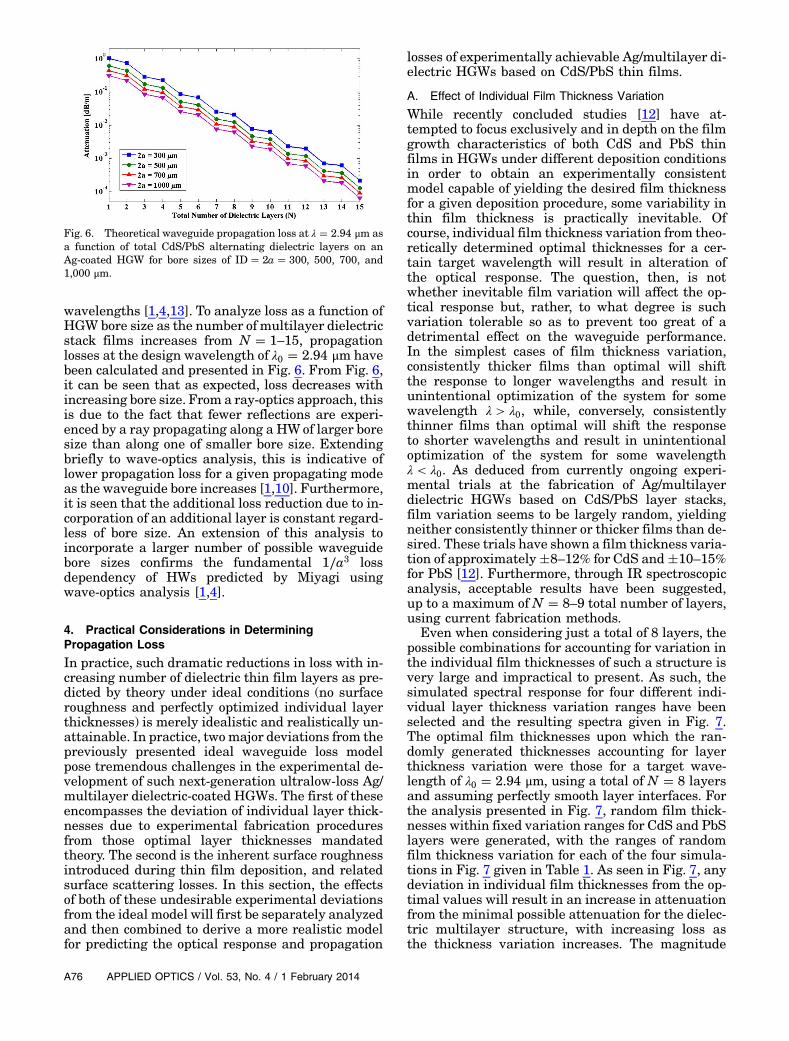
wavelengths [1,4,13]. To analyze loss as a function ofHGW bore size as the number of multilayer dielectricstack films increases from N ! 1–15, propagationlosses at the design wavelength of λ0 ! 2.94 μm havebeen calculated and presented in Fig. 6. From Fig. 6,it can be seen that as expected, loss decreases withincreasing bore size. From a ray-optics approach, thisis due to the fact that fewer reflections are experi-enced by a ray propagating along a HWof larger boresize than along one of smaller bore size. Extendingbriefly to wave-optics analysis, this is indicative oflower propagation loss for a given propagating modeas the waveguide bore increases [1,10]. Furthermore,it is seen that the additional loss reduction due to in-corporation of an additional layer is constant regard-less of bore size. An extension of this analysis toincorporate a larger number of possible waveguidebore sizes confirms the fundamental 1∕a3 lossdependency of HWs predicted by Miyagi usingwave-optics analysis [1,4].
4. Practical Considerations in DeterminingPropagation Loss
In practice, such dramatic reductions in loss with in-creasing number of dielectric thin film layers as pre-dicted by theory under ideal conditions (no surfaceroughness and perfectly optimized individual layerthicknesses) is merely idealistic and realistically un-attainable. In practice, twomajor deviations from thepreviously presented ideal waveguide loss modelpose tremendous challenges in the experimental de-velopment of such next-generation ultralow-loss Ag/multilayer dielectric-coated HGWs. The first of theseencompasses the deviation of individual layer thick-nesses due to experimental fabrication proceduresfrom those optimal layer thicknesses mandatedtheory. The second is the inherent surface roughnessintroduced during thin film deposition, and relatedsurface scattering losses. In this section, the effectsof both of these undesirable experimental deviationsfrom the ideal model will first be separately analyzedand then combined to derive a more realistic modelfor predicting the optical response and propagation
losses of experimentally achievable Ag/multilayer di-electric HGWs based on CdS/PbS thin films.
A. Effect of Individual Film Thickness Variation
While recently concluded studies [12] have at-tempted to focus exclusively and in depth on the filmgrowth characteristics of both CdS and PbS thinfilms in HGWs under different deposition conditionsin order to obtain an experimentally consistentmodel capable of yielding the desired film thicknessfor a given deposition procedure, some variability inthin film thickness is practically inevitable. Ofcourse, individual film thickness variation from theo-retically determined optimal thicknesses for a cer-tain target wavelength will result in alteration ofthe optical response. The question, then, is notwhether inevitable film variation will affect the op-tical response but, rather, to what degree is suchvariation tolerable so as to prevent too great of adetrimental effect on the waveguide performance.In the simplest cases of film thickness variation,consistently thicker films than optimal will shiftthe response to longer wavelengths and result inunintentional optimization of the system for somewavelength λ > λ0, while, conversely, consistentlythinner films than optimal will shift the responseto shorter wavelengths and result in unintentionaloptimization of the system for some wavelengthλ < λ0. As deduced from currently ongoing experi-mental trials at the fabrication of Ag/multilayerdielectric HGWs based on CdS/PbS layer stacks,film variation seems to be largely random, yieldingneither consistently thinner or thicker films than de-sired. These trials have shown a film thickness varia-tion of approximately(8–12% for CdS and(10–15%for PbS [12]. Furthermore, through IR spectroscopicanalysis, acceptable results have been suggested,up to a maximum of N ! 8–9 total number of layers,using current fabrication methods.
Even when considering just a total of 8 layers, thepossible combinations for accounting for variation inthe individual film thicknesses of such a structure isvery large and impractical to present. As such, thesimulated spectral response for four different indi-vidual layer thickness variation ranges have beenselected and the resulting spectra given in Fig. 7.The optimal film thicknesses upon which the ran-domly generated thicknesses accounting for layerthickness variation were those for a target wave-length of λ0 ! 2.94 μm, using a total of N ! 8 layersand assuming perfectly smooth layer interfaces. Forthe analysis presented in Fig. 7, random film thick-nesses within fixed variation ranges for CdS and PbSlayers were generated, with the ranges of randomfilm thickness variation for each of the four simula-tions in Fig. 7 given in Table 1. As seen in Fig. 7, anydeviation in individual film thicknesses from the op-timal values will result in an increase in attenuationfrom the minimal possible attenuation for the dielec-tric multilayer structure, with increasing loss asthe thickness variation increases. The magnitude
Fig. 6. Theoretical waveguide propagation loss at λ ! 2.94 μm asa function of total CdS/PbS alternating dielectric layers on anAg-coated HGW for bore sizes of ID ! 2a ! 300, 500, 700, and1,000 μm.
A76 APPLIED OPTICS / Vol. 53, No. 4 / 1 February 2014

of increase in loss due to film thickness variation islargely dependent on both the magnitude indeviation from the optimal thickness for each layeras well as on the deviation across all layers. However,with the degree of film thickness variation exploredin this study, the increased loss from the correspond-ing ideal system is not nearly as detrimental as thatposed by surface roughness scattering, as will be dis-cussed in detail in the following section.
In analyzing the effect of film thickness variationon propagation loss, it must be noted that variationof the innermost layer is of particular importanceand has the greatest effect on loss out of any otherlayer in the multilayer structure. To stress the im-portance of proper innermost film thickness as deter-mined by Eqs. (9) and (10) for an odd and evennumber of dielectric layers, respectively, Fig. 8 gives
the spectra for optimized and nonoptimized inner-most layer thicknesses for N ! 7 and N ! 8, respec-tively. In Fig. 8(a), for a structure with N ! 7, thedotted spectrum represents the response for an Ag/multilayer HGW in which all layers, including the in-nermost CdS layer, are optimized for λ0 ! 2.94 μmwhile the solid spectrum represents the responsein which all layers, including the innermost CdSlayer, have thicknesses optimized for λ0 ! 2.94 asgiven by Eq. (8) [thus the innermost CdS layer thick-ness is not modified accordingly as per Eq. (9)].Figure 8(b) gives a similar analysis, but for a struc-ture with N ! 8 in which the innermost PbS layerhas been optimized as required according to Eq. (10)(dotted spectrum), and for the case in which it hasnot been modified as such and retains the optimalthickness of the other PbS layers in the structure.The impact of modifying the innermost layer thick-ness as previously discussed on the optical responseat the target wavelength is clearly evident, with asharp increase in loss seen when it has not beenoptimized, as given by Eqs. (9) and (10) for an odd(α ! 1.42 versus 1.09 × 10⁻² dB∕m) and even(α ! 0.29 versus 8.80 × 10⁻³ dB∕m) number of layers,respectively. Thus, it is critical to tailor the thicknessof the innermost film depending on the total numberof layers to shift the inherent interference peak
Fig. 7. Theoretical waveguide propagation in the near andmid-IR for random individual film variation about optimal film thicknesses forλ ! 2.94 μmwithN ! 8 CdS/PbS alternating layers on an Ag-coated HGWof ID ! 700 μmwith film variation ranges of (a) CdS∶( 5–7%,PbS∶( 7–10%, (b) CdS∶( 8–10%, PbS∶( 11–14%, (c) CdS∶( 11–13%, PbS∶( 15–18%, and (d) CdS∶( 14–16%, PbS∶( 19–22%with nofilm variation spectrum for comparison.
Table 1. Variation Ranges for Simulated Losses
Variation Range
CdS PbS
Fig. 7(a) (5–7% (7–10%Fig. 7(b) (8–10% (11–14%Fig. 7(c) (11–13% (15–18%Fig. 7(d) (14–16% (19–22%
1 February 2014 / Vol. 53, No. 4 / APPLIED OPTICS A77

occurring at the target wavelength and ensuretrue optimization of the multilayer dielectric stackin enhancing the reflectance and reducing theloss.
B. Effect of Surface Roughness Scattering
In practice, it is impossible to achieve ideal films voidof any surface roughness and, as such, investigatingthe effect of surface roughness on propagation loss isessential. In the presence of surface roughness, theFresnel transmission and reflection coefficients be-tween the ith and ith − 1 layers [Eqs. (4a)–(4d)] mustbe modified to account for scattering losses due toan irregular interface. Matsuura and Harrington[15] have suggested the following modification ofthese coefficients to account for interface surfaceroughness:
ρσi−1;i ! ρi−1;i exp%−12"2k0 · σi−1;i ·ni sin"γi##2
&; (12a)
τσi−1;i!τi−1;i
×exp%−12"k0 ·σi−1;i ·"ni sin"γi#−ni−1 sin"γi−1###2
&;
(12b)
where k0 is the free space wavenumber, σi−1;I is theRMS surface roughness between the ith and ith − 1layers, n is the refractive index of the layer materialin the ith and ith − 1 layers, respectively, and γ is thecompliment to the angle of refraction, (γi ! 90 − θiand γi−1 ! 90 − θi−1) in the ith and ith − 1 layers, re-spectively. These modified Fresnel coefficients arecalculated for s and p polarizations and used toproceed with the calculation for the reflectance coef-ficient [Eqs. (5)–(7)]. It should, furthermore, be notedthat surface roughness is a compounding effect, withthe ith − 1 layer having a total surface roughnessequal to that of the underlying ith layer in additionto any further surface roughness arising from
the deposition of the ith layer. Considering thiscontinuously compounding additive effect, the intro-duction of any surface roughness can quickly have adramatically detrimental effect on loss, increasinggreatly as the total number of deposited layersincreases. In practice, it is therefore essential tominimize surface roughness contributed during eachsubsequent layer deposition procedure.
To examine the magnitude of the detrimentaleffects of surface roughness on the overall opticalresponse of Ag/multilayer dielectric-coated HGWsin a methodological manner, we consider once morea 700 μm ID Ag/multilayer-coated HGW in which alldielectric layer film thicknesses are optimized for λ !2.94 μm (average film thicknesses not accounting forvariation due to surface roughness). Furthermore,for initial spectral analysis, the total number of di-electric layers will be held constant at N ! 8. In con-trast to previous analysis, however, the effects ofsurface roughness will now be taken into account,where it is assumed that each layer, including theunderlying Ag film, contribute an RMS surfaceroughnesses, σRMS, of 0, 10, 20, 30, and 40 nm forthe various simulations presented. Figure 9 givesthe calculated spectral response for individual layerand substrate RMS surface roughnesses of 10, 20,30, and 40 nm, respectively, with that for σRMS ! 0(dotted spectrum), being included in each analysisfor direct comparison. The highly detrimental effectof increasing surface roughness, holding all otherparameters constant is clearly visible, with an over-all increase in loss throughout the entire spectralrange covered. Particularly, it can be seen that theloss at the design wavelength quickly increaseswith increasing surface roughness, surpassing thatachievable with only a single CdS dielectric film withσRMS ! 0 nm (α ≈ 0.44 dB∕m) at individual layer sur-face roughness contributions of σRMS ! 30–40 nm(α ≈ 0.32–0.65 dB∕m) despite the dramatic increasein total number of dielectric layers.
Further analysis focusing on attenuation as afunction of both total number of dielectric layersand individual layer RMS surface roughness is given
Fig. 8. Theoretical waveguide propagation in the near and mid-IR with individual film thicknesses optimized for λ ! 2.94 μm withoptimized and nonoptimized innermost layer thicknesses for (a) N ! 7 and (b) N ! 8 total dielectric layers.
A78 APPLIED OPTICS / Vol. 53, No. 4 / 1 February 2014
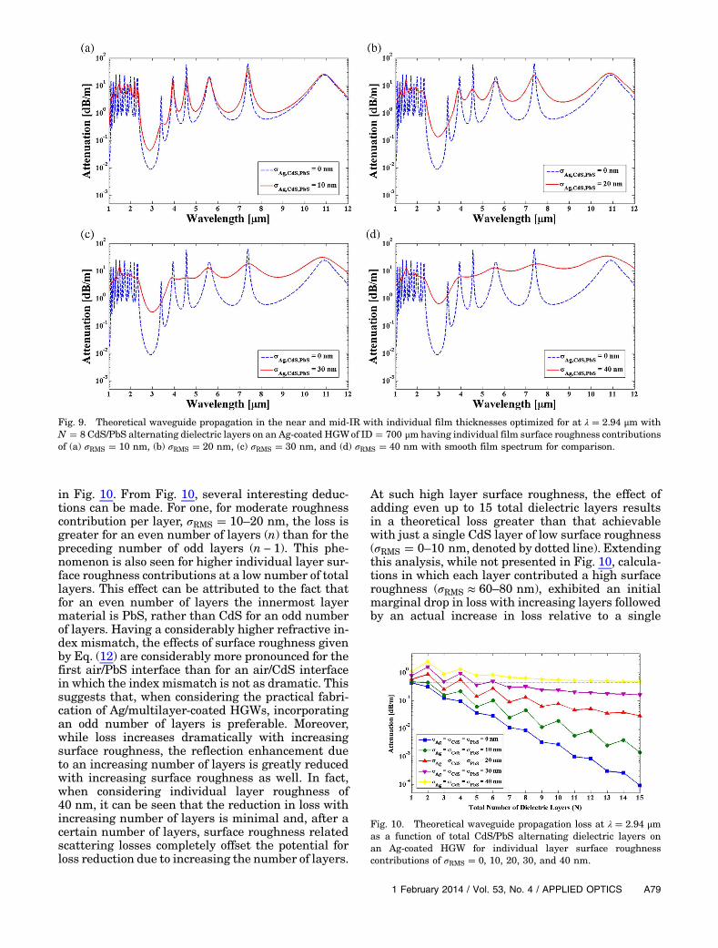
in Fig. 10. From Fig. 10, several interesting deduc-tions can be made. For one, for moderate roughnesscontribution per layer, σRMS ! 10–20 nm, the loss isgreater for an even number of layers (n) than for thepreceding number of odd layers (n − 1). This phe-nomenon is also seen for higher individual layer sur-face roughness contributions at a low number of totallayers. This effect can be attributed to the fact thatfor an even number of layers the innermost layermaterial is PbS, rather than CdS for an odd numberof layers. Having a considerably higher refractive in-dex mismatch, the effects of surface roughness givenby Eq. (12) are considerably more pronounced for thefirst air/PbS interface than for an air/CdS interfacein which the index mismatch is not as dramatic. Thissuggests that, when considering the practical fabri-cation of Ag/multilayer-coated HGWs, incorporatingan odd number of layers is preferable. Moreover,while loss increases dramatically with increasingsurface roughness, the reflection enhancement dueto an increasing number of layers is greatly reducedwith increasing surface roughness as well. In fact,when considering individual layer roughness of40 nm, it can be seen that the reduction in loss withincreasing number of layers is minimal and, after acertain number of layers, surface roughness relatedscattering losses completely offset the potential forloss reduction due to increasing the number of layers.
At such high layer surface roughness, the effect ofadding even up to 15 total dielectric layers resultsin a theoretical loss greater than that achievablewith just a single CdS layer of low surface roughness(σRMS ! 0–10 nm, denoted by dotted line). Extendingthis analysis, while not presented in Fig. 10, calcula-tions in which each layer contributed a high surfaceroughness (σRMS ≈ 60–80 nm), exhibited an initialmarginal drop in loss with increasing layers followedby an actual increase in loss relative to a single
Fig. 9. Theoretical waveguide propagation in the near and mid-IR with individual film thicknesses optimized for at λ ! 2.94 μm withN ! 8 CdS/PbS alternating dielectric layers on an Ag-coated HGWof ID ! 700 μmhaving individual film surface roughness contributionsof (a) σRMS ! 10 nm, (b) σRMS ! 20 nm, (c) σRMS ! 30 nm, and (d) σRMS ! 40 nm with smooth film spectrum for comparison.
Fig. 10. Theoretical waveguide propagation loss at λ ! 2.94 μmas a function of total CdS/PbS alternating dielectric layers onan Ag-coated HGW for individual layer surface roughnesscontributions of σRMS ! 0, 10, 20, 30, and 40 nm.
1 February 2014 / Vol. 53, No. 4 / APPLIED OPTICS A79
dielectric film with the addition of further layers.Finally, it should be noted that unacceptably highindividual layer contribution surface roughnessvalues (σRMS > 90 nm) yielded only an increase inattenuation with the addition of any subsequent di-electric layers. Thus, in practice, surface roughnesspresents a great challenge in achieving the theoreti-cal loss reduction potential of Ag/multilayer dielec-tric-coated HGWs, with the total number of layersthat may be deposited to yield an actual reductionin propagation loss being limited by the individualsurface roughness magnitudes achieved via thecorresponding thin film deposition procedure andthe degree of additive surface roughness with theaddition of subsequent films.
C. HGW Model Accounting for Experimental Variations
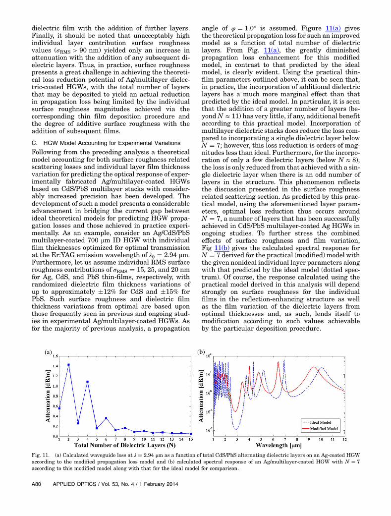
Following from the preceding analysis a theoreticalmodel accounting for both surface roughness relatedscattering losses and individual layer film thicknessvariation for predicting the optical response of exper-imentally fabricated Ag/multilayer-coated HGWsbased on CdS/PbS multilayer stacks with consider-ably increased precision has been developed. Thedevelopment of such a model presents a considerableadvancement in bridging the current gap betweenideal theoretical models for predicting HGW propa-gation losses and those achieved in practice experi-mentally. As an example, consider an Ag/CdS/PbSmultilayer-coated 700 μm ID HGW with individualfilm thicknesses optimized for optimal transmissionat the Er:YAG emission wavelength of λ0 ! 2.94 μm.Furthermore, let us assume individual RMS surfaceroughness contributions of σRMS ! 15, 25, and 20 nmfor Ag, CdS, and PbS thin-films, respectively, withrandomized dielectric film thickness variations ofup to approximately (12% for CdS and (15% forPbS. Such surface roughness and dielectric filmthickness variations from optimal are based uponthose frequently seen in previous and ongoing stud-ies in experimental Ag/multilayer-coated HGWs. Asfor the majority of previous analysis, a propagation
angle of φ ! 1.0° is assumed. Figure 11(a) givesthe theoretical propagation loss for such an improvedmodel as a function of total number of dielectriclayers. From Fig. 11(a), the greatly diminishedpropagation loss enhancement for this modifiedmodel, in contrast to that predicted by the idealmodel, is clearly evident. Using the practical thin-film parameters outlined above, it can be seen that,in practice, the incorporation of additional dielectriclayers has a much more marginal effect than thatpredicted by the ideal model. In particular, it is seenthat the addition of a greater number of layers (be-yondN ≈ 11) has very little, if any, additional benefitaccording to this practical model. Incorporation ofmultilayer dielectric stacks does reduce the loss com-pared to incorporating a single dielectric layer belowN ! 7; however, this loss reduction is orders of mag-nitudes less than ideal. Furthermore, for the incorpo-ration of only a few dielectric layers (below N ≈ 8),the loss is only reduced from that achieved with a sin-gle dielectric layer when there is an odd number oflayers in the structure. This phenomenon reflectsthe discussion presented in the surface roughnessrelated scattering section. As predicted by this prac-tical model, using the aforementioned layer param-eters, optimal loss reduction thus occurs aroundN ! 7, a number of layers that has been successfullyachieved in CdS/PbS multilayer-coated Ag HGWs inongoing studies. To further stress the combinedeffects of surface roughness and film variation,Fig 11(b) gives the calculated spectral response forN ! 7 derived for the practical (modified) model withthe given nonideal individual layer parameters alongwith that predicted by the ideal model (dotted spec-trum). Of course, the response calculated using thepractical model derived in this analysis will dependstrongly on surface roughness for the individualfilms in the reflection-enhancing structure as wellas the film variation of the dielectric layers fromoptimal thicknesses and, as such, lends itself tomodification according to such values achievableby the particular deposition procedure.
Fig. 11. (a) Calculated waveguide loss at λ ! 2.94 μm as a function of total CdS/PbS alternating dielectric layers on an Ag-coated HGWaccording to the modified propagation loss model and (b) calculated spectral response of an Ag/multilayer-coated HGW with N ! 7according to this modified model along with that for the ideal model for comparison.
A80 APPLIED OPTICS / Vol. 53, No. 4 / 1 February 2014

5. Conclusion
In this study, a theoretical model for predicting theoptical response, in particular the propagation lossof HGWs, incorporating any number of reflection-enhancing dielectric thin-film(s) is presented. Thismodel, based on ray-optics analysis, lends itself togreat versatility, in particular relative to those pre-viously presented in the literature, mostly due tothe incorporation of the highly flexible transfer ma-trix method for determining the reflectance of theparticular Ag/single or multilayer dielectric innerHGW surface structure. In particular, the transfermatrix method is highly advantageous relative toother methods for calculating this reflectance, dueto its inherent ability to calculate wavelength depen-dent reflectance of the structure for any number ofdielectric layers while simultaneously accountingfor deviations in the individual structure layers fromideal, such as individual film variation and surfaceroughness, without appreciable modification of thesimulation algorithm other than the specific layerparameters. As such, analysis of Ag/multilayer-coated HGWs based on practical CdS/PbS alternat-ing layer thin film structures is extended well beyondthe ideal model and the effects of increasing surfaceroughness and individual thin film thickness varia-tion as a function of increasing the number of totalCdS/PbS alternating layers is thoroughly examined.Such analysis is then combined to derive a muchmore precise practical model for determining propa-gation losses in Ag/multilayer-coated HGWs, conse-quently achieving a theoretical model which muchmore closely approaches experimentally achievedpropagation losses. While this model is not a perfectmatch to experimentally achieved losses as it cannotaccurately account for further experimental errorand random imperfections and assumes completetransparency of CdS and PbS thin films across thenear and mid-IR λ ! 1–12 μm region, it provides amuch more advanced, practical, and accurate modelfor predicting propagation loss in HGWs and, assuch, provides a much more invaluable tool forthe engineering and design of Ag/multilayer-coatedHGWs relative to widely used idealistic models.
Through such a practical model, the effects ofindividual layer surface roughness and thicknessvariation from optimal values on HGW propagationlosses has been thoroughly analyzed and comparedto those predicted by theory not accounting for thesepractical considerations. In particular, the impor-tance of achieving adequate individual layer filmthicknesses has been investigated, with analysisshowing that achieving an adequate innermost filmthickness depending on the total number of structurelayers has a highly pronounced effect on the achiev-able propagation loss for the desired target wave-length. Furthermore, extensive analysis of theeffect of film surface roughness on loss concludes thatincreased surface roughness has a much more pro-nounced detrimental effect on loss than film thick-ness variation. In particular, it was shown that
even a relatively small increase in individual layersurface roughness greatly reduces the reflection-enhancing effects of incorporating an additionalnumber of CdS/PbS alternating layers. This effectis so detrimental in fact that, given a high enoughsurface roughness of the individual layers in thestructure, the benefit of incorporating additionallayers decreases significantly with increasing sur-face roughness, even yielding an increase in loss withincreasing total number of layers. In practice, theparticular optical response will depend on a numberof experiment specific achievable parameters, mostnotably the total number of layers in the structure,the individual layer variation from optimal for agiven target wavelength, and the individual layersurface roughness contribution and, as such, thesemust be modified accordingly in the practical modelderived in this study. Most notably, given typical ex-perimental parameter values achieved using currentdeposition procedures, it has been shown that the in-corporation of additional CdS/PbS alternating layersfor maximum transmission at λ0 ! 2.94 μm is onlybeneficial up to a certain number of total layers, afterwhich this becomes only marginally advantageousand does not offset the risks posed by the depositionof subsequent layers through current experimentalprocedures.
References1. J. A. Harrington, Infrared Fiber Optics and Their Applications
(SPIE, 2004).2. D. Rabii and J. A. Harrington, “Measurement and control of
thin film uniformity in hollow glass waveguides,” Opt. Eng.38, 2009–2015 (1999).
3. J. A. Harrington and V. Gopal, “Method, and article of themethod, for fabricating a hollow waveguide,” U.S. Patent7,315,675 (January 1 2008).
4. M. Miyagi and S. Kawakami, “Design theory of dielectric-coated circular metallic waveguides for infrared transmis-sion,” J. Lightwave Technol. LT-2, 116–126 (1984).
5. S. J. Orfanidis, Electromagnetic Waves and Antennas (RutgersUniversity, 2010).
6. J. D. Joannopoulos, S. G. Johnson, R. D. Mead, and J. N. Winn,Photonic Crystals: Molding the Flow of Light, 2nd Ed.(Princeton University, 2008).
7. E. Hecht, Optics, 3rd Ed. (Addison Wesley Longman, 1998).8. O. S. Heavens, Optical Properties of Thin Film Solids, 1st ed.
(Dover Publications, 1991).9. B. E. A. Saleh and M. C. Teich, Fundamentals of Photonics
(Wiley, 1991).10. R. J. George, “New dielectric thin film coatings for Ag and Cu
coated hollow infrared waveguides,” Ph.D. dissertation(Rutgers University, 2004).
11. V. Gopal and J. A. Harrington, “Deposition and characteriza-tion of metal sulfide dielectric coatings for hollow glass wave-guides,” Opt. Express 11, 3182–3187 (2003).
12. C. M. Bledt, J. E. Melzer, and J. A. Harrington, “Investigationof metal sulfide optical thin film growth in low-loss IRhollow glass waveguides,” Opt. Mater. Express, 3, 1397–1407(2013).
13. M. Miyagi and S. Kawakami, “Waveguide loss evaluation bythe ray-optics method,” J. Opt. Soc. Am. 73, 486–489 (1983).
14. Y. Matsuura, M. Saito, and M. Miyagi, “Loss characteristicsof circular hollow waveguides for incoherent infrared light,”J. Opt. Soc. Am. A 6, 423–427 (1989).
15. Y. Matsuura and J. A. Harrington, “Hollow glass wave-guides with three-layer dielectric coating fabricated by
1 February 2014 / Vol. 53, No. 4 / APPLIED OPTICS A81

chemical vapor deposition,” J. Opt. Soc. Am. A 14, 1255–1259(1997).
16. M. Saito, S. Sato, and M. Miyagi, “Loss characteristics ofinfrared hollow waveguides in multimode transmission,” J.Opt. Soc. Am. A 10, 277–282 (1993).
17. E. D. Palik and G. Ghosh, Handbook of Optical Constants ofSolids (Academic, 1998).
18. C. M. Bledt, J. E. Melzer, and J. A. Harrington, “Theoreticaland experimental investigation of infrared properties oftapered silver/silver halide-coated hollow waveguides,” Appl.Opt. 52, 3703–3712 (2013).
19. Y. Fink, J. N. Winn, S. Fan, J. Michel, C. Chen, J. D.Joannopoulos, and E. L. Thomas, “A dielectric omnidirectionalreflector,” Science 282, 1679–1682 (1998).
A82 APPLIED OPTICS / Vol. 53, No. 4 / 1 February 2014