the centre for process innovation · the centre for process innovation is the uk’s national...
TRANSCRIPT

From innovation to commercialisation
Printable ElectronicsThe Centre for Process Innovation
Printable Electronics
The Centre for Process InnovationFrom innovation to commercialisation
The Centre for Process Innovation is the UK’s national technology and innovation centre to serve and support the process manufacturing industries. We are chosen by key industry leaders and SMEs to develop, prove, prototype and scale up the next generation of products and processes.
We work across a range of technology platforms, each of which have the potential to generate a substantial impact on the future of manufacturing. We provide product and process development facilities and expertise in industrial biotechnology and biorefining, formulation and flexible manufacturing, printable electronics and biologics with the overall aim of creating less waste, cleaner, more efficient and more economic products and processes.
Our open innovation model enables our clients to develop products and prove processes with minimal risk. We provide assets and expertise so our customers can demonstrate the process and prove it is feasible before investing substantial amounts of money in capital equipment and training. New products and processes can be proven; on paper, in the lab and in the plant before being manufactured at an industrial scale.
By utilising our proven assets and expertise companies can take their products and processes to market faster. There is no down time in production as all of the process development is completed off-line.
Better Products, FasterWe help our clients to produce better products with increased quality and performance. We can create processes with higher yields and reduced manufacturing time with faster conversion of raw materials or feedstock to product.
Low Cost, Low Waste Manufacturing We enable companies to decrease capital and manufacturing costs by facilitating batch to continuous processes, increased automation and reduced manufacturing time. We help reduce and reuse wastes, utilise natural materials and decrease reliance on fossil fuels.
The High Value Manufacturing Catapult is a partnership between industry and government, which is a catalyst for the future growth and success of manufacturing in the UK. Its long-term goal is to stimulate growth in the manufacturing sector and grow the sector’s contribution to UK GDP to a level more commensurate with that of competitor economies. It does this by helping businesses accelerate new concepts (often started in research institutions) to commercial reality (where they can be funded through market sources). In doing so, the Catapult reduces companies’ risk in innovation, and it enables the UK to address market needs in key areas, making the country more competitive on the global stage.
The High Value Manufacturing Catapult combines the strengths of seven UK technology and innovation centres, each focusing on major underpinning manufacturing technologies. The Catapult brings these centres together to develop cross sector manufacturing capabilities, which can span from raw materials to finished processes. It also enables innovation to cut across sectors by bringing together businesses from diverse industries and giving them access to a pool of world-class expertise, equipment and processes invested and supported by UK government.

Our facilities include:
• Inkjet Flex®; roll to roll inkjet printing of copper-based flexible circuits
• A specialist roll to roll line for the printing, coating and patterning of a range of organic and inorganic solution-based coatings
• 1250m2 of class 1000 (ISO 6) and class 100 (ISO 5) cleanrooms and associated laboratory space
• 300mm wide roll to roll wet coat prototyping and processing in a class 1000 cleanroom
• Full lithography and subtractive patterning suite (eg. plasma etch)
• Additive pattern printing equipment inc. Litrex and Dimatix ink jets and Optomec aerosol jet
• Fully equipped materials preparation and formulation laboratory with characterisation instrumentation for rheometry, thermal (DSC, TGA) properties, FTIR, and surface energy
• Batch and roll to roll Atomic Layer Deposition for high-integrity conformal coatings
• Batch and continuous sputter coating in a class 1000 cleanroom environment
• An Integrated Smart Systems line capable of performing flexo, gravure, offset litho and rotary screen printing
• Large scale process development toolsets based on robotic handling with cassette to cassette-based transfers including: • Large-area high-resolution coating for OSSL and PV applications • Industry compatible coat-bake-develop and dry or wet-etch cluster tools • In line sputter coating • UV stepper exposure tool • CD and overlay measurement
• Comprehensive measurement and characterisation equipment collated via customised informatics software
Printable Electronics at CPI
Introduction
CPI offers world class, open access capability for the scale up and commercialisation of new, innovative printed electronic products and applications. Our facilities and expertise provide clients with the environment to understand how their products and processes perform under manufacturing conditions and accelerate their commercial realisation.
CPI focuses on the integration and manufacture of new innovative electronic devices, developing the technologies that will drive the manufacturing process forward. These new processes, including the printing of electronic functionality, open up a host of design opportunities and will lead to the creation of a range of future electronic applications in key market sectors such as print and packaging, healthcare, built environment, automotive and aerospace.
The integration of electronics with flexible form factors increases the freedom for product designers to embed technology and functionality into their designs, creating the opportunity for new, innovative components that are wireless, smarter, interactive, conformable, thinner, lightweight, rugged and able to blend into the
surrounding environment. These new ways of manufacturing electronics will give rise to a wide range of new, novel applications such as flexible displays for mobile devices, smart therapeutic bandages for managing and monitoring recovery of wounds, wearable electronics for monitoring and improving performance, wireless medical devices for rapid diagnostics using printed sensors, conformable lighting and intelligent packaging for consumer goods and industrial products, to name but a few.
CPI is also working with its extensive networks of partners to develop new techniques and processes that will overcome some of the innovation challenges in printable electronics, such as the need for low cost ultra high performance barrier materials.

Our ServicesWhat we offer
With a range of cost effective services, the highly skilled team at CPI can help to guide you from concept to finished product.
In the development of new electronic products and processes, our experienced scientists, engineers, scale up experts, process operators
and commercialisation specialists are able to take projects from early concepts through to innovative products.
CPI has a significant track record in working with SMEs to help them move through the innovation phase in turning their research ideas into commercial applications that utilise printed electronics.
CPI helps SMEs to identify and overcome their innovation challenges by providing technical expertise coupled with development and scale up facilities. We can help companies to understand the feasibility of their new product or process in a phased way that reduces risk for both the company and their investors.
Some of the companies currently incubating at our National Printable Electronics Centre include:
• NeuDrive - flexible OTFT materials provider• Polar OLED - flexible device supplier• PolyPhotonix - healthcare• PragmatIC - flexible IC• Silent Sensors - device manufacturer• SmartKem - semiconductors for flexible OLED
displays
Comprehensive facilities and scale-up expertise
Incubation Support for SMEs
POLYPHOTONIX
Prototyping, Demonstration and Scale Up
Product and Process Development
Materials Investigation
Consultancy
Business and Funding Support
Incubator Space
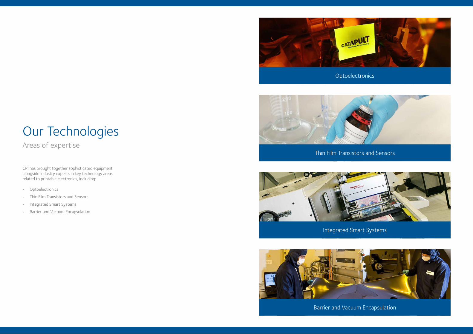
Our TechnologiesAreas of expertise
CPI has brought together sophisticated equipment alongside industry experts in key technology areas related to printable electronics, including:
• Optoelectronics
• Thin Film Transistors and Sensors
• Integrated Smart Systems
• Barrier and Vacuum Encapsulation
Thin Film Transistors and Sensors
Optoelectronics
Integrated Smart Systems
Barrier and Vacuum Encapsulation

Opto Electronics
CPI has extensive capability to support the development, scale-up and characterisation of organic light emitting diode (OLED), organic photovoltaic (OPV) and light emitting electrochemical cell applications.
Offering a versatile equipment set, CPI allows customers to scale up their products and processes supporting feasibility proof of concept at small scale (100mm), sheet-to-sheet operations at GEN 2 (370x470mm) and roll to roll operations at pilot production scale.
Proof of Concept
CPI provides small scale (100-150mm substrate size) glove boxes with spin coating / evaporation technology that supports material and device design feasibilty studies.
These systems focus on quick turnaround, proof of concept studies where the onus is on understanding the material and electrical characteristics, thereby aiding development of
the device structure by speeding up process development and aid troubleshooting. The systems are typically manually loaded by the operator and are situated in a Class 1000 clean room environment.
Pilot Production
In order to scale up an optimised material set or device design, CPI offers an OLED/OPV prototyping line situated in a Class 100 clean room environment. Here the emphasis is on ensuring optimised manufacturing protocols. Substrates are transferred within dedicated processing cassettes with manual intervention kept to a minimum. Minimising defectivity within an OLED/OPV structure is a pre-requisite in guaranteeing device yield as the technology scales
OLED, organic photovoltaic and light emitting, electro-chemical technologies
up to larger substrate sizes. A typical lighting structure can consist of 8-10 layers with layer thicknesses of < 50nm. CPI’s pilot prouction scale system is dedicated to processing both air sensitive and non air sensitive material sets for the production of devices on substrates up to 200mm2. The tool can accommodate the processing of both small molecule and solution based polymer materials and includes both slot die and spin coating techniques. Evaporation technology provides both inorganic cathode and organic small molecule capability. Device performance and lifetime are enhanced by the use of a dedicated encapsulation module to apply getters and adhesives. Fully automated robotic control, cassette to cassette handling and HEPA filtered laminar flow modules provide a unique environment to support high yield, low defect device production.
The high resolution wide area line also has the ability to handle substrates of size 8 inch, 12 inch and GEN 2 scale (370mm x 470mm) The
pilot line features sputter, dry etch, wet etch and cleaning capability and provides the ability to produce high quality lighting devices at pilot-production scale.
Roll to Roll Production
CPI also provides further scale up capability in the form of a 300mm web roll to roll coater for the printing of a range of organic material sets. The system comprises of both slot die and screen printing capabilities, with options to upgrade to 500mm web width and to incorporate other printing techniques such as reverse gravure.
The roll to roll machine houses a complementary encapsulation module, configured to allow the organic devices manufactured within the coater to be laminated with a barrier film. The tool provides protection to the device from water and oxygen ingress, both of which are known to be detrimental to device performance and lifetime.

Thin Film Transistors and Sensors
CPI has significant experience of working with clients to formulate a wide range of functional inks for printable electronics applications including sensors and organic thin film transistors; and using electronic materials, from graphene and carbon nanotubes to bio-materials and organic semiconductors.
Working with CPI, companies can develop and characterise new ink formulations applicable for a number of printing techniques such as inkjet and aerosol jet, gravure, flexographic, offset lithographic and screen. We combine expertise in chemistry and device physics with advanced processing knowledge to produce optimal performance and stability from organic electronic device applications. CPI can also help to develop inks suitable for slot die and spin coating allowing companies to quickly scale up and integrate their new inks into a range of electronic products.
Our facility is conveniently collocated with CPI’s National Formulation and Graphene Application Centres, bringing together a multi-partner network that spans key knowledge partners and SME innovation enablers and providing industry-trained experts and open-access facilities to companies to develop and scale up advanced formulated products. By utilising our underpinning
dispersion technologies, CPI provides the capability and experience to help companies to produce stable formulations that are suitable to scale up from the lab and into printed electronics based applications at pilot production scale. In addition, we can also help companies to select and optimise solvent systems, surfactants and resins.
Driving flexible electronic devices
CPI can offer:
• Evaluation and development of inks for printed electronics applications
• Materials formulation development • High resolution patterning and process
development for displays • Device design expertise • Analytical capability• Incubator space

Integrated Smart Systems
The Internet of Things promises to be one of the most revolutionary transformations in technology since the emergence of the Internet, with predictions indicating that more than 50 billion devices will be connected by 2020.
The commercialisation of associated applications requires devices which combine sensing, energy source, processing power and communications with a thin, flexible form factor. This is best achieved by integrated smart systems; adopting a hybrid approach where the processing power of conventional electronics is combined with the form factor and cost benefits of printable electronics. The manufacture of such devices requires a mix of capability such as placement techniques; adhesion, connectivity and encapsulation, all of which are housed at CPI.
CPI’s open access facilities and knowledge allows clients to test, develop and scale up a range of intelligent devices including smart labels, intelligent ticketing, printed switching, printed sensing, smart packaging and also
wireless based applications such as Radio Frequency Identification (RFID) and Near-Field Communication (NFC). Working with CPI companies can develop their specific applications from initial device design, right through to the pilot production volumes needed for market testing and investment purposes.
CPI’s capability includes a high speed R2R electronics integration tool based on a Mühlbauer TAL 15000 to enable the manufacture of thin, flexible sensing systems for applications relevant to the Internet of Things. The tool integrates thin film and conventional electronics (packaged or bare die) onto circuits printed on reels of polymer film or paper up to 350mm wide. CPI also provides access to inkjet, flexo, gravure, offset litho and rotary screen printing processes.
Rapid Prototyping of Flexible Copper Circuits with Inkjet Flex®
CPI’s Inkjet Flex® is a revolutionary two-stage print and plate process that enables copper to be printed onto PET substrates. The technology is applicable for a range of applications including printed antennae, sensors, electrodes, flexible pcbs and other components suitable for machine to machine communication devices.
The Inkjet Flex® capability allows clients to upload their copper based circuit designs and rapidly turn these designs into printed prototypes for initial feasibility and new product development work. Inkjet Flex® is capable of producing copper features on flexible PET film using a continuous roll to roll printing and plating process. Samples are costed by the metre and can be produced on both clear and opaque substrates.
Above: Inkjet Flex®, flexible copper circuit printing at CPI
Combining the benefits of conventional and printable electronics
CPI can offer:
• Prototyping, demonstration and scale-up of RFID, NFC, smart packaging, labelling and machine to machine communication devices
• Testing, validation and optimisation of speciality inks: surface roughness, conductivity, scratch resistance, adhesion, sintering and high magnification microscopy
• Substrate evaluation• Formulations and analytical capability• Incubator space

Barrier and Vacuum Encapsulation
CPI has extensive experience in the deposition and characterisation of barrier layers. We offer access to a wide variety of thin-film deposition systems including batch and roll to roll atomic layer deposition (ALD), roll to roll sputtering and also a range of other sputtering and vacuum coating technologies.
CPI is engaged in a wide range of projects initially focussing on thin-film barrier technology for long-lasting and efficient flexible electronic devices. Further developments, up to pilot scale, are targeted in printable electronics applications in the display, photovoltaics, lighting and sensor fields with both rigid and flexible substrates utilising batch and processing techniques.
CPI’s equipment includes:
• Roll to roll atomic layer deposition• Batch atomic layer deposition• Pilot scale roll to roll sputtering • In-line and batch sputtering • In-line HiTUS sputtering coater (low ion
energy bombardment during film growth) • Analysis, characterisation and metrology
High performance large area coatings and processes
CPI can offer:
• Access to a wide variety of thin-film deposition systems
• Industry experts in a wide range of vacuum processing and deposition technologies
• Expertise in combining vacuum coatings with more conventional coating technologies
• Expertise in a wide range of applications, including barrier and other coatings for application in printed electronics, optical, photovoltaic and other applications
• Access to a network of coating support and analytical capabilities, including barrier permeation characterisation

CPI’s expertise in printable electronics can be applied to a range of market applications, which have the potential for significant impact on the future of manufacturing in the UK.
CPI focuses on the integration and manufacturing of new innovative electronic devices, developing the technologies that will drive the manufacturing process forward. The printing of electronic
functionality opens up a host of design opportunities and will lead to the creation of a range of future electronic applications in key market sectors.
Our Markets
CPI is focused on the commercialisation of new innovative technologies for the aviation sector. We offer product and process development capability in application areas such as:
• Intelligent sensing
• The Internet of Things
• Flexible, lightweight display screens
• Printed lighting
• Flexible solar technologies
• Head-up displays
Aerospace
With the potential for improved control and operation through printed sensors, conformable integrated displays and lighting, printable electronics will provide users with a new and improved driving experience alongside improvements in the manufacturing process.
CPI is working on bringing the following applications to the automotive market:
• Intelligent sensing
• Flexible, lightweight display screens
• Printed lighting
• Flexible solar technologies
• Head-up displays
Automotive and Transport
Automotive and Transport
Built Environment
Aerospace
Energy and Environment
Print and Packaging
Materials
Healthcare
Pharmaceuticals
Household Goods
Electronics and IT
Food and Drink Personal Care
Retail and Consumer Goods

CPI is working on the new product development of the following for the food and drink industry:
• Sensors in manufacturing
• Packaging compliance
• Intelligence in logistics
Due to its design freedom, printed electronics provide the opportunity to incorporate electronic functionality into a wide range of medical and healthcare products. The technology encompasses thin, flexible, conformable and lightweight electronics opening up a range of opportunities for the sector including:
• Smart packaging
• Non-invasive screening
• Light therapies
• Healthcare photonics
• Printed sensing
Food and DrinkHealthcare
CPI is working on the commercialisation of the following applications for the household goods market:
• Smart packaging and the Internet of Things
• Printed sensors in manufacturing and logistics tracking
CPI is working on the commercialisation of smart packaging and the Internet of Things for the print and packaging sector.
Printable electronics is adding value to print through its convergence with the internet and its ease of integration with Near-Field Communication (NFC) and Radio Frequency Identification (RFID) technologies, including:
• Smart packaging
• Smart labelling
• Anti-counterfeiting
• Track and trace
• Product monitoring
Household GoodsPrint and Packaging

CPI provides specialist expertise in the new product development of printed sensing capability for applications in the materials and chemicals industry. We can work with you to develop innovations in:
• Printed sensors in manufacturing
• Intelligence in logistics
CPI is focused on the commercialisation of new innovative technologies for the built environment. We offer product and process development capability in application areas such as:
• Flexible, lightweight display screens
• Printed lighting
• Flexible solar technologies
• Intelligent sensing
MaterialsBuilt Environment
CPI provides specialist expertise in new product development for printed solar technologies such as PV, OPV and BIPV.
Innovations in solar technology will facilitate new designs for solar panels with thin, lightweight encapsulating envelopes and flexible form factors. The technology will make solar panels suitable for applications where flexibility, product shape and aesthetic value are important. Flexible photovoltaic technology will allow designers to apply and integrate solar energy into a wide range of surfaces within the built environment such as building roofs, walls, windows, lightings and fabric applications.
CPI is focused on the commercialisation of new innovative technologies for the personal care industry. We offer product and process development capability in application areas such as:
• Sensors in manufacturing
• Intelligence in packaging
• Intelligence in logistics
Energy and the EnvironmentPersonal Care

CPI focuses on the integration and manufacture of new innovative electronic devices, developing the technologies that will drive the manufacturing process forward. These new products and processes, including the printing of electronic functionality open up a host of design opportunities and will lead to the creation of a range of future electronic applications.
We provide new product development capability in the following areas:
• Flexible, lightweight display screens
• Printed lighting
• Flexible solar technologies
• Intelligent sensing
Electronics and IT
CPI is working on the commercialisation of the following applications for the retail sector:
• Wearable electronics
• Smart packaging and the Internet of Things
• Dynamic price displays
• Flexible, lightweight display screens
• Printed lighting
• Sensors in manufacturing
• Printed intelligence in logistics
CPI provides specialist expertise in the new product development of printed sensing capability to improve the quality and administration of pharmaceutical products right across the supply chain. We are working to develop innovations in:
• Smart packaging
• Sensors in manufacturing
• Intelligence in logistics
Retail and Consumer GoodsPharmaceuticals

00938-170120-01
To find out more about our full range of services visit: www.uk-cpi.com call: +44 (0)1740 625 700
Industrial Biotechnology and Biorefining
Printable Electronics Formulation Biologics
Centre for Process InnovationThe Neville Hamlin Building, Thomas Wright Way, NETPark, Sedgefield, TS21 3FG, United Kingdom
Copyright © 2014-2017 Centre for Process Innovation Limited. All rights reserved.
T: +44 (0)1740 625 700E: [email protected]: www.uk-cpi.com