texturing the cathode of white organic light-emitting...
TRANSCRIPT

Texturing the cathode of white organic light-emitting diodes with a latticeof nanoscale scatterers for enhanced light out-coupling
Ardavan Oskooia)
Department of Electrical Engineering and Computer Science, University of Michigan, Ann Arbor,Michigan 48109, USA
(Received 13 November 2014; accepted 16 January 2015; published online 28 January 2015)
The external quantum efficiency of white organic light-emitting diodes is often limited by light
out-coupling losses due to surface plasmons. We demonstrate how texturing of the metal-cathode
surface using a two-dimensionally periodic lattice of nanoscale scatterers with limited disorder can
be used to reduce plasmonic losses while simultaneously enhancing both the light out-coupling and
the spontaneous-emission rate of the excitons. We use electrodynamic simulations and statistical
modeling to explore the relationship between the topology of the surface texture and its corre-
sponding scattering efficiency. From this, we outline attributes of textures that can most enhance
device performance. VC 2015 AIP Publishing LLC. [http://dx.doi.org/10.1063/1.4907253]
The development of organic light-emitting diodes
(OLEDs), particularly those based on small-molecule phos-
phorescent materials,1 has led to a number of commercial
applications arising from their nearly 100% internal quantum
efficiency (IQE). Yet the external quantum efficiency (EQE),
which takes into account the light-extraction efficiency, still
has significant room for improvement despite intensive work
based on a number of different designs including microlens
arrays, low-index microstructured grids, high-index substrates,
oriented-dipole emitters, photonic crystals, and plasmonic out-
coupling schemes.2,3 In this work, we describe a design for a
nanostructured, white-emitting OLED (WOLED), operating
under the conditions of broad spectral bandwidth and isotropic
emitters, which enhances both the light-extraction efficiency
and the spontaneous-emission rate of the excitons.4–8 Our
approach, which does not require any additional materials,
involves applying a texture to the metal-cathode surface where
its topology consists of a two-dimensionally periodic lattice of
nanoscale scatterers augmented with limited disorder. This
design fulfills two objectives: (1) to enhance coupling to the
surface-plasmon polaritons (SPPs) to boost the rate of exciton
decay and (2) to radiatively scatter out as many of these other-
wise non-radiative modes over the shortest possible distance.
We employ a three-dimensional electromagnetic solver9,10 to
simulate the optical properties of a WOLED by statistically
modeling the temporal dynamics of exciton recombination and
with this show that while there is some degree of flexibility in
the choice of the morphology of the scatterers and the topology
of the lattice, their exact dimensions must be carefully tuned to
optimize device performance.
While several previous works have focused on reducing
losses from surface plasmons via texturing,11–16 there
appears to be a lack of designs for reducing such losses while
simultaneously enhancing the light-extraction efficiency and
the spontaneous-emission rate of excitons compared to an
unpatterned device. Our work is used to identify the most
effective properties of a general class of textures where the
topology is comprised of a 2D lattice of scatterers; a
particularly advantageous one is shown in Figure 1(a). This
design is found to be effective in extracting light over a broad
bandwidth and hence is potentially suitable for WOLEDs17
used in solid-state lighting. Broad spectral out-coupling makes
the design more challenging given that nanophotonic effects
typically rely on coherent resonant phenomena that are re-
stricted to narrow spectral bandwidths and preferred orienta-
tions.18–20 Finally, we demonstrate that limited disorder in the
array which is often encountered in fabrication can improve
the out-coupling efficiency.
The optical properties of the WOLEDs were computed
using full 3D electrodynamic simulations via MEEP—an
open-source finite-difference time-domain (FDTD) software
tool.9 Using MEEP, we can compute the Poynting vector
over a wide spectral bandwidth using a short temporal
pulse, simulate a large supercell with its distributed-memory-
parallelism and subpixel-smoothing features, and model
the temporal dynamics of radiative exciton decay with
nanometer-scale resolution using its customizable-source and
pervasive-interpolation capabilities. We start with a planar,
bottom-emitting WOLED comprised of four separate stacked
layers: an Al cathode (thickness 100 nm), an organic film
comprising hole-transporting (40 nm) and emissive (20 nm)
and electron-transporting (40 nm) layers, an indium-tin oxide
(ITO) transparent conductive film (100 nm), on top of a semi-
infinite glass substrate with a square profile of length L, as
shown in Figure 1(a). The refractive indices of the glass,
organic, and ITO layers are nglass¼ 1.45, nORG¼ 1.8, and
nITO¼ 1.8, where losses in the ITO have been ignored since
this layer is optically thin, and our primary focus is on plas-
monic losses. The Al cathode is a lossy metal modeled using a
Drude-Lorentzian fit that spans the WOLED emission spec-
trum.21 We compute the wavelength-dependent total power
emitted by ten different incoherent (i.e., random phase) elec-
tric point-dipole sources evenly distributed along a vertical
line centered within the emissive layer (EML), in addition to
the power in the glass, organic, and ITO layers (i.e., wave-
guide modes), the cathode/organic interface (i.e., surface-
plasmon polaritons), and the absorption at the cathode. The ra-
tio of the power in each of these components to the totala)[email protected]
0003-6951/2015/106(4)/041111/5/$30.00 VC 2015 AIP Publishing LLC106, 041111-1
APPLIED PHYSICS LETTERS 106, 041111 (2015)
This article is copyrighted as indicated in the article. Reuse of AIP content is subject to the terms at: http://scitation.aip.org/termsconditions. Downloaded to IP:
141.213.51.236 On: Wed, 28 Jan 2015 16:49:16

dipole emission therefore gives the fraction of the total power
that is distributed among the different device regions. Ten sep-
arate simulations are made, which provide sufficient conver-
gence, for both planar and textured cathodes and the results
averaged due to the random nature of the sources and in some
cases the texture itself.
The total power emitted by a dipole source at a point in
the EML is proportional to the local density of states (LDOS)
at that point22 which, in turn, is proportional to the rate of
spontaneous emission obtained via Fermi’s Golden Rule.23–25
FDTD is used to compute the spontaneous-emission-rate
enhancement factor defined as the ratio of the average power
radiated per dipole in the nanostructured compared to the
unpatterned device using identical coherent point sources in a
single simulation. For calculations involving structures with
textured surfaces, we use 16 000 electric-dipole emitters that
are evenly distributed within a volume, centered within the
EML, of rectangular cross-section of length a so as to sample
the LDOS over the entire EML. In all cases, we use a resolu-
tion of 10 nm/pixel which, in combination with its subpixel-
smoothing function, allows MEEP to model features whose
scale is only a few nanometers.
Figures 2(a) and 2(b) show the simulated results for two
orthogonal dipole orientations: parallel and perpendicular to
the layers of an untextured WOLED with L¼ 5 lm. Here, the
total emitted power is separated into its components of glass,
combined cathode/organic interface and organic/ITO wave-
guide (Al þ ORG þ ITO), and Al absorption. The average of
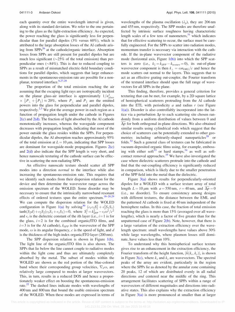
FIG. 1. (a) Schematic of a bottom-emitting OLED with a square profile of length L comprised of an aluminum (Al) cathode, electron-transporting (ETL) and
emissive (EML) and hole-transporting (HTL) organic (ORG) layers, and indium-tin oxide (ITO) transparent anode, on top of a glass substrate. The thickness
of each layer is marked. The surface of the ETL consists of a lattice with periodicity a of Al hemispheres with radius r protruding into the organic. Random dis-
order is introduced into the lattice by perturbing each hemisphere by an amount Dp whose values range between 0 and �Dp. Incoherent electric point-dipole
sources are positioned within the EML to simulate the temporal dynamics of exciton recombination. (b) Dispersion relation of the SPP at the cathode/organic
interface of the OLED. The red portion of the band corresponds to the operating range of white-emitting OLEDs: dashed lines extending from the frequency
axis are modes with vacuum wavelengths of 400 nm to 800 nm with associated wavevectors (2p/kp, where kp is the wavelength of the plasma oscillation) noted
on the horizontal axis. The shaded region is the light cone of the organic/ITO film.
FIG. 2. Optical properties of a planar
OLED. (a) and (b) Fraction of total
dipole power in each of the three com-
ponents of the OLED with L¼ 5 lm:
glass, combined cathode/organic inter-
face and organic/ITO waveguide (Al þORG þ ITO), and Al absorption for
(a) parallel and (b) perpendicular
dipoles relative to the substrate plane.
(c) and (d) Fraction of total dipole
power, averaged over the wavelength
spectrum, in the three device regions
as functions of propagation length (L)
under the cathode for dipoles with ori-
entation (c) parallel and (d) perpendic-
ular to the substrate plane. Losses in
the metal due to the surface-plasmon
polaritons are dominant.
041111-2 Ardavan Oskooi Appl. Phys. Lett. 106, 041111 (2015)
This article is copyrighted as indicated in the article. Reuse of AIP content is subject to the terms at: http://scitation.aip.org/termsconditions. Downloaded to IP:
141.213.51.236 On: Wed, 28 Jan 2015 16:49:16
each quantity over the entire wavelength interval is given,
along with its standard deviation. We refer to the one pertain-
ing to the glass as the light-extraction efficiency. As expected,
the power reaching the glass is significantly less for perpen-
dicular than for parallel dipoles (3% versus 60%), which is
attributed to the large absorption losses of the Al cathode aris-
ing from SPPs26 at the cathode/organic interface. Absorption
losses from SPPs are still present for parallel dipoles but are
much less significant (�25% of the total emission) than per-
pendicular ones (�84%). This is due to reduced coupling to
SPPs as a result of mismatched electric-field boundary condi-
tions for parallel dipoles, which suggests that large enhance-
ments in the spontaneous-emission rate are possible for a non-
planar, textured interface.6,27,28
The proportion of the total emission reaching the air
assuming that the escaping light rays are isotropically incident
on the planar glass-air interface is approximately 1=n2glass
� 13
P? þ 23
PkÞ � 20%�
, where P? and Pk are the emitted
powers into the glass for perpendicular and parallel dipoles,
respectively.2,3 We plot the average power in each region as a
function of propagation length under the cathode in Figures
2(c) and 2(d). The fraction of light absorbed by the Al cathode
monotonically increases, whereas the waveguide component
decreases with propagation length, indicating that most of the
power outside the glass resides within the SPPs. For perpen-
dicular dipoles, the Al absorption reaches approximately 95%
of the total emission at L¼ 10 lm, indicating that SPP losses
are dominant for waveguide-mode propagation. Figures 2(c)
and 2(d) also indicate that the SPP length is very short, and
hence nanoscale texturing of the cathode surface can be effec-
tive in scattering the non-radiating SPPs.
An effective nanoscale texture should scatter all SPP
modes into a direction normal to the interface while also
increasing the spontaneous-emission rate. This requires that
we identify such modes from their dispersion relation for the
device and then determine the wavevector range across the
emission spectrum of the WOLED. Some disorder may be
necessary to ensure that the intrinsically narrowband resonant
effects of ordered textures span the entire spectrum.18–20,29
We can compute the dispersion relation for the WOLED
configuration in Figure 1(a) by solving30 ð�1�3S22 þ �2
2S1S3ÞtanhðS2dÞþ�2S2ð�3S1þ�1S3Þ¼0, where S2
i ¼ k2SPP��ix2=c2
and �i is the dielectric constant of the ith layer (i.e., i¼1 is for
the glass, i¼2 is for the combined organic/ITO films, and
i¼3 is for the Al cathode), kSPP is the wavevector of the SPP
mode, x is its angular frequency, c is the speed of light, and dis the thickness of the high-index organic/ITO layer (200 nm).
The SPP dispersion relation is shown in Figure 1(b).
The light line of the organic/ITO film is also shown. The
SPPs that lie below the line cannot couple to radiative modes
within the light cone and thus are ultimately completely
absorbed by the metal. The subset of modes within the
WOLED are shown as the red portion of the blue-colored
band where their corresponding group velocities, rkx, are
relatively large compared to modes at larger wavevectors.
This, in turn, results in a reduced DOS and hence a propor-
tionately weaker effect on boosting the spontaneous-emission
rate.22 The dashed lines indicate modes with wavelengths of
400 nm and 800 nm that bound the usable emission spectrum
of the WOLED. When these modes are expressed in terms of
wavelengths of the plasma oscillation (kp), they are 206 nm
and 455 nm, respectively. The SPP modes are therefore unaf-
fected by intrinsic surface roughness having characteristic
length scales of a few tens of nanometers,31 which indicates
that for effective scattering to occur, the surface must be care-
fully engineered. For the SPPs to scatter into radiation modes,
momentum transfer is necessary via interaction with the cath-
ode. If the in-plane wavevector component of the radiative
mode (horizontal axis, Figure 1(b)) into which the SPP scat-
ters is zero (i.e., kk ¼ kSPP� ktexture¼ 0), its out-of-plane
wavevector component is then k? ¼ xnORG=c and hence the
mode scatters out normal to the layers. This suggests that to
act as an effective grating out-coupler, the Fourier transform
of the textured interface should span the full range of wave-
vectors for all SPPs in the plane.
This finding, therefore, provides a general criterion for
texturing that can be met, for example, by a 2D square lattice
of hemispherical scatterers protruding from the Al cathode
into the ETL with periodicity a and radius r (see Figure
1(a)). Disorder is also controllably incorporated into the lat-
tice via a perturbation Dp to each scattering site chosen ran-
domly from a uniform distribution of values between 0 and
Dp for both orthogonal in-plane directions. We also obtained
similar results using cylindrical rods which suggest that the
choice of scatterers can be potentially extended to other geo-
metries including arbitrarily-shaped nanoparticles28 or
folds.32 Such a general class of textures can be fabricated in
vacuum-deposited organic films using, for example, emboss-
ing with either soft33 or hard stamps,34 as well as soft-
contact removal approaches.35 We have also investigated the
case where dielectric scatterers protrude into the cathode and
find that the out-coupling efficiency is significantly reduced
in comparison, which is likely due to the smaller penetration
of the SPP field into the metal than the dielectric.
Figure 3(a) shows results for perpendicularly-oriented
dipoles for a WOLED with a surface texture array of total
length L¼ 10 lm with a¼ 550 nm, r¼ 40 nm, and Dp¼ 0
(i.e., no disorder). To ensure consistency among designs
with different textures, the distance between the EML and
the patterned Al cathode is fixed at 40 nm independent of the
hemisphere radius. In this case, the fraction of total emission
reaching the glass is more than 15% (averaged over all wave-
lengths), which is nearly a factor of five greater than for the
unpatterned case of Figure 2(b). Note, however, that there is
a large variation of the extraction efficiency over the wave-
length spectrum: small wavelengths have values above 30%
while large wavelengths, where plasmon losses still domi-
nate, have values less than 10%.
To understand why this hemispherical surface texture
gives rise to an enhancement in the extraction efficiency, the
Fourier transform of the height function, j~hðkx; kyÞj, is shown
in Figure 3(c), where kx and ky are wavevectors. The spectral
peaks of the array are evident, particularly in the region
where the SPPs lie as denoted by the annular zone containing
20 peaks, 12 of which are distributed evenly in all radial
directions and centered near the middle of the ring. This
arrangement facilitates scattering of SPPs within a range of
wavevectors of different magnitudes and directions into radi-
ative states. This also explains why the extraction efficiency
in Figure 3(a) is more pronounced at smaller than at larger
041111-3 Ardavan Oskooi Appl. Phys. Lett. 106, 041111 (2015)
This article is copyrighted as indicated in the article. Reuse of AIP content is subject to the terms at: http://scitation.aip.org/termsconditions. Downloaded to IP:
141.213.51.236 On: Wed, 28 Jan 2015 16:49:16
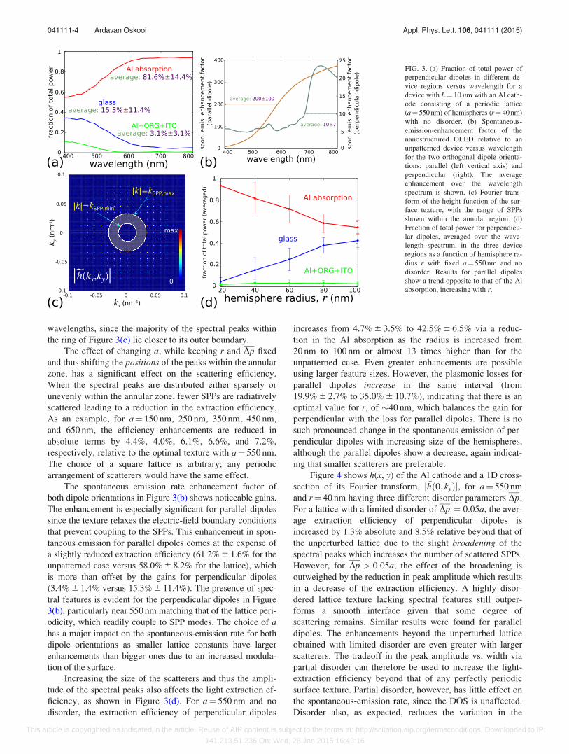
wavelengths, since the majority of the spectral peaks within
the ring of Figure 3(c) lie closer to its outer boundary.
The effect of changing a, while keeping r and Dp fixed
and thus shifting the positions of the peaks within the annular
zone, has a significant effect on the scattering efficiency.
When the spectral peaks are distributed either sparsely or
unevenly within the annular zone, fewer SPPs are radiatively
scattered leading to a reduction in the extraction efficiency.
As an example, for a¼ 150 nm, 250 nm, 350 nm, 450 nm,
and 650 nm, the efficiency enhancements are reduced in
absolute terms by 4.4%, 4.0%, 6.1%, 6.6%, and 7.2%,
respectively, relative to the optimal texture with a¼ 550 nm.
The choice of a square lattice is arbitrary; any periodic
arrangement of scatterers would have the same effect.
The spontaneous emission rate enhancement factor of
both dipole orientations in Figure 3(b) shows noticeable gains.
The enhancement is especially significant for parallel dipoles
since the texture relaxes the electric-field boundary conditions
that prevent coupling to the SPPs. This enhancement in spon-
taneous emission for parallel dipoles comes at the expense of
a slightly reduced extraction efficiency (61.2% 6 1.6% for the
unpatterned case versus 58.0% 6 8.2% for the lattice), which
is more than offset by the gains for perpendicular dipoles
(3.4% 6 1.4% versus 15.3% 6 11.4%). The presence of spec-
tral features is evident for the perpendicular dipoles in Figure
3(b), particularly near 550 nm matching that of the lattice peri-
odicity, which readily couple to SPP modes. The choice of ahas a major impact on the spontaneous-emission rate for both
dipole orientations as smaller lattice constants have larger
enhancements than bigger ones due to an increased modula-
tion of the surface.
Increasing the size of the scatterers and thus the ampli-
tude of the spectral peaks also affects the light extraction ef-
ficiency, as shown in Figure 3(d). For a¼ 550 nm and no
disorder, the extraction efficiency of perpendicular dipoles
increases from 4.7% 6 3.5% to 42.5% 6 6.5% via a reduc-
tion in the Al absorption as the radius is increased from
20 nm to 100 nm or almost 13 times higher than for the
unpatterned case. Even greater enhancements are possible
using larger feature sizes. However, the plasmonic losses for
parallel dipoles increase in the same interval (from
19.9% 6 2.7% to 35.0% 6 10.7%), indicating that there is an
optimal value for r, of �40 nm, which balances the gain for
perpendicular with the loss for parallel dipoles. There is no
such pronounced change in the spontaneous emission of per-
pendicular dipoles with increasing size of the hemispheres,
although the parallel dipoles show a decrease, again indicat-
ing that smaller scatterers are preferable.
Figure 4 shows h(x, y) of the Al cathode and a 1D cross-
section of its Fourier transform, j~hð0; kyÞj, for a¼ 550 nm
and r¼ 40 nm having three different disorder parameters Dp.
For a lattice with a limited disorder of Dp ¼ 0:05a, the aver-
age extraction efficiency of perpendicular dipoles is
increased by 1.3% absolute and 8.5% relative beyond that of
the unperturbed lattice due to the slight broadening of the
spectral peaks which increases the number of scattered SPPs.
However, for Dp > 0:05a, the effect of the broadening is
outweighed by the reduction in peak amplitude which results
in a decrease of the extraction efficiency. A highly disor-
dered lattice texture lacking spectral features still outper-
forms a smooth interface given that some degree of
scattering remains. Similar results were found for parallel
dipoles. The enhancements beyond the unperturbed lattice
obtained with limited disorder are even greater with larger
scatterers. The tradeoff in the peak amplitude vs. width via
partial disorder can therefore be used to increase the light-
extraction efficiency beyond that of any perfectly periodic
surface texture. Partial disorder, however, has little effect on
the spontaneous-emission rate, since the DOS is unaffected.
Disorder also, as expected, reduces the variation in the
FIG. 3. (a) Fraction of total power of
perpendicular dipoles in different de-
vice regions versus wavelength for a
device with L¼ 10 lm with an Al cath-
ode consisting of a periodic lattice
(a¼ 550 nm) of hemispheres (r¼ 40 nm)
with no disorder. (b) Spontaneous-
emission-enhancement factor of the
nanostructured OLED relative to an
unpatterned device versus wavelength
for the two orthogonal dipole orienta-
tions: parallel (left vertical axis) and
perpendicular (right). The average
enhancement over the wavelength
spectrum is shown. (c) Fourier trans-
form of the height function of the sur-
face texture, with the range of SPPs
shown within the annular region. (d)
Fraction of total power for perpendicu-
lar dipoles, averaged over the wave-
length spectrum, in the three device
regions as a function of hemisphere ra-
dius r with fixed a¼ 550 nm and no
disorder. Results for parallel dipoles
show a trend opposite to that of the Al
absorption, increasing with r.
041111-4 Ardavan Oskooi Appl. Phys. Lett. 106, 041111 (2015)
This article is copyrighted as indicated in the article. Reuse of AIP content is subject to the terms at: http://scitation.aip.org/termsconditions. Downloaded to IP:
141.213.51.236 On: Wed, 28 Jan 2015 16:49:16

extraction efficiency over the wideband spectrum: for per-
pendicular dipoles, the standard deviation of the averaged
extraction efficiency is reduced monotonically by 5.2% abso-
lute for Dp ¼ 0:4a compared to the unperturbed case. Peak
broadening arising from lattice disorder can also be realized
by introducing small non-uniformities into the size and mor-
phology of the scatterers, which again can be used to extend
the range of applicable textures.
In summary, we have shown how texturing of the metal-
cathode surface using a topology based on a 2D lattice of scat-
terers can be used to reduce losses from SPPs and enhance
both the light-extraction efficiency and the spontaneous-
emission rate of excitons in WOLEDs compared with an
unpatterned device. The choice of the morphology of the scat-
terers and the topology of the lattice has some degree of flexi-
bility although their exact dimensions must be carefully tuned
to optimize device performance. Our design does not require
any additional materials and hence can be used to explore
optimal designs for different OLED layering schemes and
emission spectra. Texturing of the cathode surface based on
the designs presented in this work may potentially lead to
marked improvements in the overall efficiency of OLEDs.
We thank Professor Stephen R. Forrest at the University
of Michigan for numerous helpful comments and suggestions.
We are also grateful to Brock Palen of the Center for
Advanced Computing for technical assistance with running
MEEP on the Flux high-performance cluster and to Behrouz
Shiari for access to the NNIN/C computing resources at the
UofM. This work also made use of the Extreme Science and
Engineering Discovery Environment (XSEDE) at the Texas
Advanced Computing Center, which was supported by
National Science Foundation (Grant No. ACI-1053575). This
work was partially supported by Universal Display Corp.
1M. A. Baldo, D. F. O’Brien, Y. You, A. Shoustikov, S. Sibley, M. E.
Thompson, and S. R. Forrest, Nature 395, 151 (1998).2K. Saxena, V. K. Jain, and D. S. Mehta, Opt. Mater. 32, 221 (2009).3W. Brutting, J. Frischeisen, T. D. Schmidt, B. J. Scholz, and C. Mayr,
Phys. Status Solidi A 210, 44 (2013).4V. Bulovic, V. B. Khalfin, G. Gu, P. E. Burrows, D. Z. Garbuzov, and S.
R. Forrest, Phys. Rev. B 58, 3730 (1998).5S. Nowy, B. C. Krummacher, J. Frischeisen, N. A. Reinke, and W.
Brutting, J. Appl. Phys. 104, 123109 (2008).6G. Sun, J. B. Khurgin, and R. A. Soref, Appl. Phys. Lett. 90, 111107
(2007).7K. Y. Yang, K. C. Choi, and C. W. Ahn, Appl. Phys. Lett. 94, 173301 (2009).8M. Furno, R. Meerheim, S. Hofmann, B. Lussem, and K. Leo, Phys. Rev.
B 85, 115205 (2012).9A. F. Oskooi, D. Roundy, M. Ibanescu, P. Bermel, J. D. Joannopoulos, and
S. G. Johnson, Comput. Phys. Commun. 181, 687 (2010).10Advances in FDTD Computational Electrodynamics: Photonics and
Nanotechnology, edited by A. Taflove, A. Oskooi, and S. G. Johnson
(Artech House, Boston, 2013).11W. L. Barnes, J. Mod. Opt. 45, 661 (1998).12J. M. Lupton, B. J. Matterson, I. D. W. Samuel, M. J. Jory, and W. L.
Barnes, Appl. Phys. Lett. 77, 3340 (2000).13P. A. Hobson, S. Wedge, J. A. E. Wasey, I. Sage, and W. L. Barnes, Adv.
Mater. 14, 1393 (2002).14U. Geyer, J. Hauss, B. Riedel, S. Gleiss, U. Lemmer, and M. Gerken,
J. Appl. Phys. 104, 093111 (1998).15J. Frischeisen, Q. Niu, A. Abdellah, J. B. Kinzel, R. Gehlhaar, G. Scarpa,
C. Adachi, P. Lugli, and W. Brutting, Opt. Express 19, A7 (2010).16C. S. Choi, D.-Y. Kim, S.-M. Lee, M. S. Lim, K. C. Choi, H. Cho, T.-W.
Koh, and S. Yoo, Adv. Opt. Mater. 1, 687 (2013).17Y. Sun, N. C. Giebink, H. Kanno, B. Ma, M. E. Thompson, and S. R.
Forrest, Nature 440, 908 (2006).18A. Oskooi, P. Favuzzi, Y. Tanaka, H. Shigeta, Y. Kawakami, and S. Noda,
Appl. Phys. Lett. 100, 181110 (2012).19A. Oskooi, Y. Tanaka, and S. Noda, Appl. Phys. Lett. 104, 010121 (2014).20A. Oskooi, M. De Zoysa, K. Ishizaki, and S. Noda, ACS Photonics 1, 304
(2014).21A. D. Rakic, A. B. Djurisic, J. M. Elazar, and M. L. Majewski, Appl. Opt.
37, 5271 (1998).22A. Oskooi and S. G. Johnson, “Electromagnetic wave source conditions,”
in Advances in Computational Electrodynamics: Photonics andNanotechnology (Artech, Boston, 2013), Chap. 4.
23P. W. Milonni, Phys. Rep. 25, 1 (1976).24F. Wijnands, J. B. Pendry, F. J. Garcia-Vidal, P. M. Bell, P. J. Roberts, and
L. M. Moreno, Opt. Quantum Electron. 29, 199 (1997).25Y. Xu, R. K. Lee, and A. Yariv, Phys. Rev. A 61, 033807 (2000).26H. Raether, Surface Plasmons on Smooth and Rough Surfaces and on
Gratings (Springer-Verlag, New York, 1988).27R. M. Amos and W. L. Barnes, Phys. Rev. B 59, 7708 (1999).28E. Fort and S. Gressilon, J. Phys. D: Appl. Phys. 41, 013001 (2008).29J. B. Khurgin and G. Sun, Appl. Phys. Lett. 94, 221111 (2009).30J. Burke, G. Stegeman, and T. Tamir, Phys. Rev. B 33, 5186 (1986).31K. Okamoto, I. Niki, A. Shvartser, Y. Narukawa, T. Mukai, and A.
Scherer, Nat. Mater. 3, 601 (2005).32W. H. Koo, S. M. Jeong, F. Araoka, K. Ishikawa, S. Nishimura, T.
Toyooka, and H. Takezoe, Nat. Photonics 4, 222 (2010).33D. Qin, Y. Xia, and G. M. Whitesides, Nat. Protocols 5, 491 (2010).34L. J. Guo, Adv. Mater. 19, 495 (2007).35C. E. Packard, K. E. Aidala, S. Ramanan, and V. Bulovic, Langmuir 27,
9073 (2011).
FIG. 4. Schematic of the surface height function of the cathode and a 1D
cross section of its corresponding Fourier transform (with the wavevectors
of the SPP modes shown in the gray region) for three different cathode lat-
tice arrays with a¼ 550 nm and r¼ 40 nm, where the disorder �Dp is: (a)
0.05a, (b) 0.2a, and (c) 0.4a. For �Dp ¼ 0:05a, the average extraction effi-
ciency for perpendicular dipoles is increased by 1.3% absolute and 8.5% rel-
ative beyond the unperturbed lattice due to the slight broadening of the
peaks. Further increases in the disorder result in the elimination of the peaks
and hence a reduction in the extraction efficiency. In the limit of large disor-
der where no traces of the peaks remain, the extraction efficiency is still
enhanced beyond that of an unpatterned interface. Results for parallel
dipoles show similar trends.
041111-5 Ardavan Oskooi Appl. Phys. Lett. 106, 041111 (2015)
This article is copyrighted as indicated in the article. Reuse of AIP content is subject to the terms at: http://scitation.aip.org/termsconditions. Downloaded to IP:
141.213.51.236 On: Wed, 28 Jan 2015 16:49:16