testing analog and mixed-signal circuits with built-in
TRANSCRIPT

840 IEEE TRANSACTIONS ON INSTRUMENTATION AND MEASUREMENT, VOL. 56, NO. 3, JUNE 2007
Testing Analog and Mixed-Signal Circuits WithBuilt-In Hardware—A New ApproachSunil R. Das, Life Fellow, IEEE, Jila Zakizadeh, Satyendra Biswas, Member, IEEE,
Mansour H. Assaf, Member, IEEE, Amiya R. Nayak, Senior Member, IEEE,Emil M. Petriu, Fellow, IEEE, Wen-Ben Jone, Senior Member, IEEE, and
Mehmet Sahinoglu, Senior Member, IEEE
Abstract—This paper aims to develop an approach to testanalog and mixed-signal embedded-core-based system-on-chips(SOCs) with built-in hardware. In particular, oscillation-basedbuilt-in self-test (OBIST) methodology for testing analog compo-nents in mixed-signal circuits is implemented in this paper. Theproposed OBIST structure is utilized for on-chip generation ofoscillatory responses corresponding to the analog-circuit compo-nents. A major advantage of the OBIST method is that it does notrequire stimulus generators or complex response analyzers, whichmakes it suitable for testing analog circuits in mixed-signal SOCenvironments. Extensive simulation results on sample analog andmixed-signal benchmark circuits and other circuits described bynetlist in HSPICE format are provided to demonstrate the feasi-bility, usefulness, and relevance of the proposed implementations.
Index Terms—Built-in self-test (BIST), circuit under test(CUT), design-for-testability (DFT), mixed-signal test, oscillation-based BIST (OBIST), system-on-chip (SOC), test-pattern genera-tor (TPG).
I. INTRODUCTION
EVER-INCREASING applications of the analog andmixed-signal embedded-core-based system-on-chips
(SOCs) [1], in recent years, have motivated system designersand test engineers to shift their research direction to embracethis particular area of very large-scale integrated circuits andsystems to develop specifically their effective test strategies.The modern technology of manufacturing high-volume prod-ucts demands that substantial efforts be directed toward thedesign, test, and evaluation of the prototypes before the start of
Manuscript received June 15, 2005; revised December 4, 2006. This workwas supported in part by the Natural Sciences and Engineering ResearchCouncil of Canada under Grant A 4750.
S. R. Das is with the Faculty of Engineering, School of Information Tech-nology and Engineering, University of Ottawa, Ottawa, ON K1N 6N5, Canada,and also with the Department of Computer and Information Science, Collegeof Arts and Sciences, Troy University, Montgomery, AL 36103 USA.
J. Zakizadeh, A. R. Nayak, and E. M. Petriu are with the Faculty ofEngineering, School of Information Technology and Engineering, Universityof Ottawa, Ottawa, ON K1N 6N5, Canada.
S. Biswas is with the Department of Electrical Engineering Technology,Georgia Southern University, Statesboro, GA 30458 USA.
M. H. Assaf is with the University of Trinidad and Tobago, O’MearaCampus, O’Meara Industrial Park, Arima, Trinidad and Tobago.
W.-B. Jone is with the Department of Electrical and Computer Engineering,University of Cincinnati, Cincinnati, OH 45221 USA.
M. Sahinoglu is with the Department of Computer and Information Science,College of Arts and Sciences, Troy University, Montgomery, AL 36103 USA.
Color versions of one or more of the figures in this paper are available onlineat http://ieeexplore.ieee.org.
Digital Object Identifier 10.1109/TIM.2007.894223
the actual production cycle. An important objective to realizethrough detailed testing is to ensure that the manufacturedproducts are free from defects and to simultaneously guaranteethat they meet all the required specifications. Besides, theinformation that may be acquired through the process mayultimately help in increasing the product yield, thereby re-ducing the product cost. The integrated-circuit (IC) fabricationprocess involves photolithography, printing, etching, anddoping steps. In the real-world situations, none of thesesteps is ever perfect, and the resulting imperfections mayeventually lead to failures in the operation of the individualICs. Specifically, the performance of mixed-signal ICs willbe greatly degraded, since these circuits are very sensitive toeven small imperfections in any step of the fabrication process.In the digital-circuit domain, however, some of these may berather unimportant, but in mixed-signal circuits, imperfectionin the form of small capacitance between the traces can presenta significant circuit-parameter variation, thereby changing thecircuit behavior drastically. Because of the shrinking of thecircuit geometry, the circuit performance sensitivity is alsoenhanced. That is why every IC must be very rigorously testedbefore being shipped to their customers. The testing improvesthe overall quality of the final product, although it has no effecton the ICs’ manufacturing excellence. Furthermore, the testingassures the product flawlessness when implemented during thekey phases of a product development. Besides, it can also bea strategy for validating the design and checking processes.The high sensitivity of mixed-signal circuits to very smallimperfections during process implementations and their broadspecifications necessitate detailed and long performance testsas well. All these requirements eventually result in high testcost, thus forcing research efforts to be directed in the domainof mixed-signal testability [1]–[26]. Researchers are nowseeking to combine both the analog- and the digital-circuitstesting either by applying digital signals, such as serial bitstreams to drive analog circuits, or by using analog signals todrive digital circuits.
The test methodologies for digital devices are already prettywell developed [27]–[34]. In contrast, analog-test methods arestill so underdeveloped that analog test becomes a bottleneckin mixed-signal-test environment, particularly with the devel-opments of semiconductor technology with high integrationdensities and shrinking sizes. Although analog and mixed-signal-test approach takes benefit from the digital-test devel-opment and experience, analog and mixed-signal tests are still
0018-9456/$25.00 © 2007 IEEE

DAS et al.: TESTING ANALOG AND MIXED-SIGNAL CIRCUITS WITH BUILT-IN HARDWARE—A NEW APPROACH 841
far behind their digital counterparts. One obvious reason is alack of accepted test principle such as standard fault modelfor analog components. Almost all the digital test techniquesare based on single stuck-fault model, and the test generationalgorithms are evaluated by their fault coverage [29]–[34].Although the stuck-fault model for functional test is acceptable,a model for performance test is not accepted easily. The mainsources of test difficulties in digital and analog circuits arealso different; for example, the size and complexity in digitalcircuits remain a measure of test difficulty, whereas in analogand mixed-signal circuits, the behaviors of circuit signals aremuch more important than circuit sizes. A major problem in theanalog and mixed-signal-circuit testing is in defining the line ofdemarcation between a fault-free and faulty circuit, resultingin uncertainty of quantification of the product yield. However,fault coverage in analog and mixed-signal circuits can still bedefined as the percentage ratio of the number of faults detectedto the total number of possible circuit faults.
Evidently, the mixed-signal technology is in the process oftremendous development with concurrent advances in the fieldof electronic packaging, besides the shrinking sizes of ICs.The process of interfacing any system with the outside worldputs additional demands on mixed-signal circuits. In the mixed-signal environment, the analog circuits sit so close to theirdigital counterparts that it creates not only a design challengebut also a related problem in their test. The demand on mixed-signal test is thus increasing as the demand for mixed-signalICs is growing. Analog- and digital-test procedures had beena research topic for many years in industry and academia.Currently, there is a huge need for the development of mixed-signal-test methods. In general, testing is a verification processand determines whether the required circuit-design specifica-tions are met. The testing of mixed-signal circuits is alwayscomplex and challenging, and hence, semiconductor industryattempts to look for proper ways of testing so as to lower thecost of test, particularly for analog portions in mixed-signaldevices. Up to 85% of the test cost is dedicated to the analogfunctions, while analog parts typically occupy only around10% of the chip area. Thus, reduction of the test cost is avery important issue for analog parts because the cost greatlyexceeds the test cost of digital circuits.
Many parts of the mixed-signal SOCs are not accessiblefrom the outside due to SOC complexity and limited test pins.However, the accessibility of a node that is either controllableor observable in a circuit can be increased using design-for-test (DFT) strategies. Applying DFT techniques reducesthe test cost, improves product quality, and makes design-characterization and test-program development easier. To in-crease testability and controllability of internal nodes, test busesand scan chains are used. Nevertheless, the output signals haveto be transmitted through long wires in order to be measuredand processed. Analog signals will be degraded readily throughthis transmission. Therefore, the test outcome will be incorrectand production yield will be decreased. One viable solution tothis problem can be the use of built-in self-test (BIST) method-ology. BIST is a design process that provides the capabilityof solving many of the problems otherwise encountered intesting analog, mixed-signal, or digital systems. It combines
Fig. 1. Block diagram of a typical BIST environment.
the concepts of both the built-in test (BIT) and ST in one,which is termed BIST. In BIST, test generation, test application,and response verification are all accomplished through built-inhardware, which allows different parts of a chip to be testedin parallel, thereby reducing the required testing time, besideseliminating the necessity for external test equipment. As thecost of testing is becoming the single major component of themanufacturing expense of a new product, BIST thus tends toreduce manufacturing and maintenance costs through improveddiagnosis [27]–[34]. A typical BIST environment, as shown inFig. 1, uses a test-pattern generator (TPG—stimulus source)that sends its outputs to a circuit under test (CUT), and outputstreams from the CUT are fed into a test data analyzer. A faultis detected if the test sequence is different from the responseof the fault-free circuit. The test data analyzer is comprised ofa response compaction unit (RCU), storage for the fault-freeresponses of the CUT, and comparator.
The lack of standard fault model for components of analog ormixed-signal circuits, broadness of analog specifications, andincomplete test set may, however, decrease test quality for theanalog portion. Another major problem in testing analog com-ponents is in defining the line of demarcation between a fault-free and faulty circuit, resulting in uncertainty of quantificationof the product yield. In this paper, an approach to developingtest strategies for analog circuits in mixed-signal embedded-core-based SOC environments based on oscillation-based BIST(OBIST) architecture is investigated. In the process, the tech-nique for modifying a given circuit so as to make it testableis discussed based on the principles of OBIST methodology.The defined fault model and test algorithms developed for thispurpose are also explored in this paper. Results on extensivesimulations on application of the proposed implementations toa selected set of analog and mixed-signal benchmark circuits[11] and other circuits are given as well to demonstrate the fea-sibility, usefulness, and relevance of the proposed realizations.
II. MIXED-SIGNAL ICS AND OBIST
Process technology has allowed analog and mixed-signaldesigners to integrate notable amount of functionality of asystem onto a single chip. In general, there are two types ofSOCs, viz., one that has grown from the application-specific

842 IEEE TRANSACTIONS ON INSTRUMENTATION AND MEASUREMENT, VOL. 56, NO. 3, JUNE 2007
Fig. 2. Typical analog and mixed-signal SOC.
Fig. 3. Design flow of analog and mixed-signal SOCs.
IC (ASIC) world, while the other emanated from the customIC world. This kind of design is digital integration, and itis interfaced with analog devices by embedded software. Theanalog and mixed-signal blocks are integrated only when thetime and cost spent on the integration are reasonable. The lattertype of design, called analog and mixed-signal design, has high-performance and complex signal paths through both the analogand the digital components. An example of mixed-signal SOCis illustrated by Fig. 2, where the main components tend to bea digital-to-analog converter (DAC), phase-locked loop (PLL),random-access memory (RAM), logic, and other cores. Fig. 3illustrates the design flow of analog and mixed-signal SOCs.
Several fault-based test strategies have been proposed in theliterature for testing analog and mixed-signal circuits [2]–[26].The OBIST deserves special mention because it is conceptuallysimple and does not require extensive modifications of theCUT for testing. The oscillation-based-test (OBT) strategy isproposed in [8], [12], [17], and [25], which is a defect-orientedtechnique and can be applied either for online or for offlinetesting. In this test method, there is no need for either testgenerators or test specifications, which are very costly. Inapplying OBT for a system, certain aspects must be considered,however, viz., system partitioning, feedback type, necessarymeasurements, fault coverage, and others. The procedure issuch that a complex analog circuit is partitioned into functional
Fig. 4. Block diagram of OBT strategy.
building blocks, such as, operational amplifiers (Op Amps),comparators, filters, PLLs, and so on, or a combination ofthese blocks. Then, each building block is converted into anoscillator by adding the proper circuitry in order to achievesustained oscillation; the oscillation parameters are evaluatednext. A faulty circuit is detected from a deviation of its os-cillation parameters with respect to the oscillation parametersunder fault-free conditions. In view of the fact that oscillationparameters are independent of the CUT type, analog testingcan be standardized. Fig. 4 shows a block diagram of theOBT strategy. The oscillation parameters can be the frequency,amplitude, distortion, or dc level of the output signal. Althoughthis method provides high fault coverage by considering onlythe oscillation frequency, there may be some faults that maynot be correlated with the frequency. In such cases, other testparameters have to be taken into consideration. For example, asindicated in [23], the fault coverage is improved by monitoringthe supply current in addition to the oscillation frequency andoutput voltage.
Several methods are proposed to extract the oscillation pa-rameters from the output test signals. A simple technique issuggested in the study in [7] to evaluate the output signalcoming off the OBT-technique application. In this method, adelta–sigma (∆Σ) modulator is connected to the output of theCUT to provide a train of modulated pulses that contain allthe information about the output of the CUT. In order to extractthe oscillation parameters, the train of pulses is processed usingan automatic test equipment (ATE) or on-chip digital-signalprocessor. The implementation strategies for OBIST may varybased on the tradeoffs between the test time and the area over-head. In [18], three different approaches are discussed of BISTimplementations on biquad filters. The concept of switchableOp Amp (sw-Op Amp) is utilized in this paper. In the firstapproach, all the building blocks are transformed into oscil-lators simultaneously, with every stage having a comparator.Although this approach reduces the test time, extra hardware isrequired. In the second approach, only one comparator is usedsuch that each block is sequentially converted to an oscillatorby using sw-Op Amp and an analog multiplexer. In the third

DAS et al.: TESTING ANALOG AND MIXED-SIGNAL CIRCUITS WITH BUILT-IN HARDWARE—A NEW APPROACH 843
approach, sw-Op Amp is used to bypass signals from theirinputs. Only one block is converted to an oscillator at a time,while the evaluation is done sequentially. The continuity ofthe blocks can be tested by the second and third approaches,although more testing time is needed.
The OBT methodology has been applied for many cir-cuits, viz., analog-to-digital converters, filters [6], [7], [17],[21], etc. In addition, the technique has also been appliedto dual-tone multifrequency detector [18], digitally program-mable switched-current biquad [10], analog microcell [24],switched-capacitor circuits [6], and even smart sensor de-vices and complementary-symmetry metal-oxide semiconduc-tor (CMOS) microelectromechanical systems (MEMS). Themeasurement of accurate oscillation frequency can be timeconsuming. In [20], a test architecture is proposed using time-division-multiplexer (TDM) comparator. Here, the CUT isconverted into an oscillator and the oscillation waveform iscompared with two reference voltages; the results are thenstored in counters by TDM.
The technique proposed in this paper for testing analog andmixed-signal circuits based on OBIST is next explained indetail, as follows.
A. Building an Oscillator
Many techniques have been proposed in the literature forbuilding an oscillator [35]. A technique for the transforma-tion of an active RC filter into an oscillator is presented byZarnik et al. in [21]. Another way to design a sinusoidal oscil-lator from the transfer function is to connect the output terminalof the filter to the input terminal. The basic requirements foroscillation are a signal feedback from the output to the input ofproper phase and sufficient amplitude. Some oscillators use RCelements for phasing. Some others operate on the principle ofpresenting a negative resistance as the feedback element. Thedesign equations of an oscillator are determined by analyzingthe denominator of the transfer equation T (s) of the circuit. Thepoles of the denominator of the characteristic equation T (s),or equivalently the zeros of T (s), determine the time-domainbehavior and stability of the system [35]. An oscillator is onthe borderline between a stable and an unstable system andis formed when a pair of poles is on the imaginary axis. Themagnitude and phase equations of an oscillator must also beanalyzed. If the magnitude of the loop-gain is greater than oneand the phase is zero, the amplitude of oscillation will increaseexponentially until a factor in the system, such as the supplyvoltage, restricts the growth. In contrast, if the magnitude ofthe loop-gain is less than one, the amplitude of oscillation willexponentially decrease to zero.
The process of building general oscillators is different fromthat of building oscillators for testing purposes. In design-ing general oscillators, well-defined and stable oscillation fre-quency and amplitude are required. In contrast, an oscillatorthat is built from the conversion of the CUT is designedsuch that the variation of the components can be detected bymeasuring the oscillation frequency and amplitude. That means,there is no need for another circuitry (automatic gain controller)to stabilize the oscillation [26].
Fig. 5. Stuck-open and stuck-short fault models for capacitor, resistor,and MOSFET.
Converting a filter into an oscillator requires a mechanismto force the placement of a pair of poles on the jω-axis. Thegeneral biquadratic transfer function is given by
H(s) =V o(s)V i(s)
=a2s
2 + a1s+ a0
s2 + b1s+ b0
where b1 = ω0/Q, and b0 = ω20 . The relation between the pole,
pole frequency, and quality factor is given by
p1, p2 = σ ± jω = − ω0
2Q± jω0
√1 − (1/4Q2)
where ω0 is the pole frequency, and Q is the pole quality factorthat determines the distance of the poles on jω-axis in thes-plane. An infinite Q locates the poles on the jω-axis, and thiscan cause the circuit to oscillate. Therefore, in order for a filterto oscillate, the quality factor must be increased.
B. Fault Model
Faults occurring in analog circuits can be categorized in twotypes: hard faults and soft faults [2]. Hard faults or catastrophicfaults are those faults that cause the circuit performance todiffer catastrophically from normal conditions. Catastrophic-fault model is the same as stuck-fault model used in the digitaltest domain where every component can be either stuck-open orstuck-short [31], [33], [34].
Stuck-open fault results when the terminal of an analog-circuit component is not connected to the rest of the circuit,while stuck-short fault occurs when a short is created betweenthe terminals of a component. On the other hand, soft orparametric faults refer to changes in a circuit that do not affectits connectivity, resulting in circuit functions out of specifica-tions. The parametric faults can be modeled as variations ofcomponent parameters that are beyond their tolerance limits.
In this paper, only catastrophic faults are considered. Fig. 5depicts standard fault models for capacitors, resistors, and MOSfield-effect transistors (MOSFETs), where the value for theparallel resistor Rp is 10 Ω that emulates stuck-short faultand that of the series resistor Rs has a value of 100 MΩthat emulates stuck-open fault. These fault models are used inHSPICE simulations in this paper.

844 IEEE TRANSACTIONS ON INSTRUMENTATION AND MEASUREMENT, VOL. 56, NO. 3, JUNE 2007
Fig. 6. Test procedure based on OBIST approach.
C. Test Procedure
Purely analog ICs, unlike digital ICs, usually consist of rel-atively few circuit primitives such as amplifiers, comparators,etc., but many parameters must be considered for test. The testparameters are specified by designers and can be gain, offsetvoltage, slew rate, signal-to-noise ratio, bandwidth, and so on.Traditionally, analog circuits have been tested functionally forspecifications such as offset voltage, signal-to-noise ratio, etc.,and functional test is still used in wafer level and packaged tests.This is primarily due to lack of any standard fault model foranalog circuits.
In the application of the testing procedure proposed in thispaper, stuck-open and stuck-short faults are first injected atthe circuit level. These faults are described in HSPICE formatand are injected into nominal circuit descriptions. By usingthe HSPICE simulator, the transient response is then evaluated,and frequency and output voltage are measured. Fig. 6 gives aflow-chart representation of the test procedure based on OBISTapproach. In the following, we provide an overview of thedifferent steps of the procedure.
Step 1) The fault-free circuit is converted into an oscillatorand simulated, and its test parameters (oscillationfrequency and amplitude of the output signal) arederived.
Step 2) A fault list was derived from the CUT (circuitnetlist).
Step 3) The faulty netlist is generated (through faultinjection).
Fig. 7. (a) Circuit and (b) transfer characteristics.
Step 4) A simulation was done for the faulty CUT.Step 5) The fault detection was completed on comparing
the faulty-output measurements with fault-free testparameters.
Step 6) The procedure is continued until all faults areinjected.
Step 7) The circuit fault coverage was calculated.
The procedure is implemented using computer programs writ-ten in C programming language.
D. Example Inverter and Oscillation-Frequency Calculation
The proposed OBIST methodology for calculating the oscil-lation frequency is explained here by considering an exampleinverter (Fig. 7). We know that n-channel MOS (NMOS) andp-channel MOS (PMOS) complementary transistors pair formsa CMOS inverter, with the transistor gates connected together asinput and drains connected together as an output. To obtain thesymmetric characteristics, it is necessary to make the PMOS de-vice wider than NMOS such that the threshold voltage becomesVcc/2. To achieve this threshold voltage of Vcc/2, we used tochoose the width of PMOS 2.5 times wider than that of theNMOS. In order to make the CMOS inverter circuit to oscillate,the classical CMOS astable-oscillator concepts are employed.
As shown in Fig. 7, resistor R1 connects the output of theCMOS inverter (CUT, in this case) to its input and thus actsas dc negative feedback. The output of the CUT is connectedto the input of another inverter U1 directly. The output of U1
is connected to the input of the CUT through a capacitor. Thisprovides positive ac feedback.
It is considered that the input of the CUT is zero; then, theoutput of the inverter U1 is low, and there is no charge storedin the capacitor. The capacitor begins to charge through theresistor R1, since the input impedance of the CMOS inverteris quite large. As soon as the capacitor voltage exceeds thethreshold voltage of the CUT, Vth(Vth = Vcc/2), then the out-put of the CUT drops to zero. Thus, the output of U1 becomeshigh. We know that the voltage across a capacitor is continuous;therefore, the voltage difference between the two sides of thecapacitor must remain at Vcc/2. That means, when one sideof the capacitor jumps to Vcc from zero, the other side mustjump to 3Vcc/2. The voltage Vcc/2 appears on common node

DAS et al.: TESTING ANALOG AND MIXED-SIGNAL CIRCUITS WITH BUILT-IN HARDWARE—A NEW APPROACH 845
Fig. 8. Output signal of the CUT in test mode.
Fig. 9. Fault models for NMOS and PMOS transistors of inverter.
of R1 and C1, whereas the other node of R1 is zero so thatthe capacitor starts to discharge through R1. As soon as thevoltage across R1 reaches the threshold voltage Vth, the outputof the CUT transits to Vcc, and the output of the inverter U1
goes to zero. The voltage at the common node of R1 and C1 isthen pulled to −Vcc/2. Thus, the capacitor C1 starts to chargetoward Vcc.
The cycle continues to produce a square-wave output, asshown in Fig. 8. The frequency of oscillation can be determinedas follows.
During the time interval t1, when the output is low, thevoltage across the capacitor C1(νc) rises from −Vcc/2 to Vth.Substituting νc = Vth = Vcc/2 at t = t1 results in
t1 = R1C1 ln 3.
Also, during the time interval t2 when the output is high, νcfalls from 3Vcc/2 to Vth. The exponential fall of νc can bedescribed by
νc = 3Vcc/2e−t2/R1C1.
Substituting νc = Vth = Vcc/2 at t = t2 results in
T2 = R1C1 ln 3.
The period of output T can be achieved by summing t1and t2 as
T = t1 + t2
T =2R1C1 ln 3 = 2.2R1C1.
The frequency of the oscillation is given by
fosc = 1/2.2R1C1.
Fig. 10. Oscillator with stuck-open Qp.
Fig. 11. Oscillator with stuck-short Qp.
By choosing R1 = 500 kΩ, C1 = 10 nF, and R2 = 5 MΩ,the oscillation frequency is calculated as fosc = 90.9 Hz. Theoscillation frequency of the simulated circuit in HSPICE isobtained as fosc = 86.95 Hz.
Fig. 9 depicts the fault model for MOS transistors, where thevalue for the parallel resistor Rp is 10 Ω, which emulates stuck-short fault, and the series resistorRs has a value of 100 MΩ thatemulates stuck-open fault.
Fig. 10 shows the circuit configuration for testing for stuck-open fault of PMOS transistor Qp. Assuming that the input ofU1 is +5 V, its output will be zero. First of all, the capacitorC1 will start to charge through R1 until the gate voltage of Qnbecomes more than Vth (threshold voltage of Qn), or Vgs ≥Vth. Therefore, Qn will operate, and Vds of Qn will be zerofrom Vds = Vgs − Vth. Then, the output of U1 will turn high(+5 V) and stay high, since the drain of Qp has been discon-nected and has no influence on the output of Qn. A similar resultis obtained with HSPICE simulation, as shown in Fig. 12(a).

846 IEEE TRANSACTIONS ON INSTRUMENTATION AND MEASUREMENT, VOL. 56, NO. 3, JUNE 2007
Fig. 12. Outputs of astable with faults injected. (a) Output of astable when Qn is stuck-open. (b) Output of astable when Qp is stuck-open. (c) Output of astablewhen Qn is stuck-short. (d) Output of astable when Qp is stuck-short.
Fig. 13. Compensated CMOS Op Amp.
Next, we consider the stuck-short fault of the PMOS Qp,as shown in Fig. 11. Since the input of U1 is shorted toVcc, the output will always be zero. Exactly the same resultis obtained with HSPICE simulation as shown in Fig. 12(b).Fig. 12(c) and (d) depicts, respectively, the simulation resultsobtained from NMOS transistor Qn for stuck-open and stuck-short faults. Now, it is seen that by injecting any one of the fourconsidered faults to the inverter of astable causes stopping ofthe oscillation of the circuit. If any one of the transistors in theinverter circuitry becomes short or open, the output will remaineither high or low according to the injected fault. Consequently,the simulation results agree with the theory.
Fig. 14. Single Op Amp oscillator.
To inject every fault, first we find the Qp or Qn throughthe netlist file of the oscillator and then connect Rp or Rsas required for the faults. The general syntax for a MOSFETelement in an HSPICE netlist is
Mxxx nd ng ns 〈nb〉 mname 〈〈L =〉length〉 〈〈W =〉width〉 .
The syntax for a resistor is
Rxxx n1 n2 〈mname〉〈R =〉resistance.
For instance, to inject a stuck-open fault to Qp that is defined inthe netlist as
m1 inm in vccm vccm p w = 45 u l = 5 u

DAS et al.: TESTING ANALOG AND MIXED-SIGNAL CIRCUITS WITH BUILT-IN HARDWARE—A NEW APPROACH 847
TABLE ISIMULATION RESULTS FOR OP AMP
Fig. 15. Continuous-time state variable filter.
TABLE IISIMULATION RESULTS FOR CONTINUOUS-TIME STATE VARIABLE FILTER
the netlist file of the oscillator is read and “m1” is found fromthe file; then, Rs is added as follows:
m1 ccm in vccm vccm p w = 45 u l = 5 uRs inm ccm 100e + 6.
After these changes are made, the faulty circuit is simulated,and output signals observed; the frequency of oscillation isalso measured. All the faults are injected and the output sig-nals corresponding to the faults are as shown in Fig. 12, asmentioned.

848 IEEE TRANSACTIONS ON INSTRUMENTATION AND MEASUREMENT, VOL. 56, NO. 3, JUNE 2007
Fig. 16. VCVS bandpass filter.
III. SIMULATION RESULTS
Filters and Op Amps are widely used in analog and mixed-signal environments. Efficient ways to test Op Amps and filtersare necessary because of their importance in analog systems.In order to test any circuit with oscillation-based method, first,the CUT must be converted into an oscillator by adding extracircuitry as feedback. If the circuit is faulty, the convertedcircuit either will not oscillate or the oscillation frequency andvoltage will differ from those of the fault-free conditions. Someof the circuits from the analog and mixed-signal benchmarkcircuits—first release [11]—are considered in this paper forinvestigation.
A. Compensated CMOS Op Amp
The compensated CMOS Op Amp is shown in Fig. 13. Inorder to test this Op Amp, the circuit is first converted into anoscillator by adding both the negative and positive feedbacks,as depicted in Fig. 14. The Op Amp circuit has been changedinto a second-order system that has potential characteristics foroscillation. The open-loop transfer function of the circuit isgiven by
A(s) =R1 +R7
R1 + R1+R7K(s)
=R1 +R7
R1 + R1+R7GBs
=R1 +R7
R1 + s(R1+R7)GB
.
The feedback factor β of the RC feedback network is given by
β(s) =R2
R2 + 1sC3
=sR2C3
sR2C3 + 1.
The transfer function is characterized by a single pole
K(s) =K0
1 + sωp
, ωp being the pole frequency.
Since (s/ωp) 1, K(s) = K0ωp/s = GB/s, where GB is theunity gain bandwidth. If A(jω0)β(jω0) = 1, then the circuitoscillates at frequency ω0, which is calculated as
ω20 =
GBR1
(R1 +R7)R2C3.
Fig. 17. Oscillogram of output of VCVS bandpass filter in oscillation mode.
Fig. 18. Oscillogram of output of VCVS bandpass filter in test mode withfaults injected.
In fault-free situations, the oscillation frequency and out-put voltage levels are fosc = 1.9598 MHz and Vout =〈−4.6676, 4.8642〉 V, respectively.
In this case, only catastrophic faults are considered. Table Iprovides results obtained by HSPICE simulation. As is evident,the output frequency significantly deviates with any injectedfault. Only the short-at compensator resistor Rc is not detectedby frequency measurements. Hence, by considering frequencyand voltage measurements, high-fault coverage, viz. 100%,is obtained.
B. Continuous-Time State Variable Filter
The second circuit considered for demonstrating the testmethodology is a continuous-time state variable filter. Thisuniversal or continuous-time state variable filter is obtainedfrom the analog and mixed-signal benchmark circuits—firstrelease [11]. Fig. 15 shows the schematic diagram of theactive filter implemented using three Op Amps. It incorporateshigh-pass, bandpass, and low-pass filters whose outputs aredenoted by HPO, BPO, and LPO, respectively. The circuit isfirst converted into an oscillator and then simulated. Without

DAS et al.: TESTING ANALOG AND MIXED-SIGNAL CIRCUITS WITH BUILT-IN HARDWARE—A NEW APPROACH 849
TABLE IIISIMULATION RESULTS FOR VCVS FILTER
Fig. 19. Phase-shift oscillator.
any loss of generality, we use this circuit as a low-pass filter.Therefore, the defect-detection procedure is applied on thesignals measured at LPO. This is a conservative approach, asthe consideration of HPO and BPO can potentially increasethe defect-detection sensitivity due to increased observabil-ity. The transfer functions of the high-pass, bandpass, andlow-pass filters are given in the following three equations,respectively:
VHPO(s) =k
R2R3C1C2
s2 + 1QR2C1
s+ 1R2R3C1C2
VBPO(s) =k
sR2C1
s2 + 1QR2C1
s+ 1R2R3C1C2
VLPO(s) =ks2
s2 + 1QR2C1
s+ 1R2R3C1C2
where the filter gain k and quality factor Q are defined, respec-tively, as follows:
k =2R4R6
R1R2 +R1R6 +R4R6
Q =2R1R6
R1R2 +R1R6 +R4R6.
Fig. 20. Output signals of oscillator.
Fig. 21. Notch filter.
The values of the components obtained from the benchmarkcircuit specifications are
R1 =R2 = R3 = R7 = 10 kΩ, R6 = 3 kΩ
R4 =7 kΩ, and C1 = C2 = 10 nF.
Then, the oscillation frequency and voltage level under fault-free conditions are calculated as fosc = 789.66 Hz; Vout =〈−4.5476, 4.2384〉 V. For testing involving filters, all the OpAmps are considered ideal. However, from the simulation re-sults (Table II), the conclusion to be drawn is that all the faultsare detected with this method.
C. Voltage-Controlled Voltage Source (VCVS) Filter
The test methodology is demonstrated on a VCVS filter.A VCVS filter is a variation of the Sallen–Key circuit. Theunity-gain follower of the Sallen–Key circuit is replaced witha noninverting amplifier of gain greater than unity. The VCVS

850 IEEE TRANSACTIONS ON INSTRUMENTATION AND MEASUREMENT, VOL. 56, NO. 3, JUNE 2007
TABLE IVSIMULATION RESULTS FOR NOTCH FILTER
Fig. 22. Leapfrog filter.
exists in various circuit realizations like high-pass, low-pass,and bandpass filters. The resistors of the outputs of the OpAmps create a noninverting voltage amplifier cascaded to gen-erate higher order filters. When that is done, the individualfilter sections are, in general, not identical. In fact, each sectionrepresents a quadratic polynomial of the nth-order polynomialdescribing the overall filter. In this paper, a bandpass VCVSfilter is considered, as shown in Fig. 16. The center frequencyfor the VCVS bandpass filter is expressed by
ω0 =√
R1 +R2
R1R2R3C1C2.
By considering the parameters with the following values: R1 =R2 = R3 = 20 kΩ and C1 = C2 = 20 nF, the center frequencyis calculated as f0 = 562.69 Hz and the gain of the filter K ≤2.5. By choosing the appropriate value of K(K = 2.500855),the poles of the transfer function are pulled to jω-axis of thes-plane. Then, the oscillation frequency for the VCVS filterobtained by simulation is 560.99 Hz, and the amplitude rangeis 〈−0.0011843, 0.0021159〉 V. Fig. 17 illustrates the output ofVCVS filter in oscillation mode, while Fig. 18 shows the output
Fig. 23. Oscillogram of output of leapfrog filter in oscillation mode.
Fig. 24. Oscillogram of output of faulty leapfrog filter in test mode.
in test mode with the injected open fault at R2. The obtainedfault coverage is 100%. Table III gives the simulation resultsin detail.
D. Field-Effect Transistor (FET)
In this section, we demonstrate how to test a FET basedon oscillation-test methods. In order to test a transistor,an oscillator circuit with the transistor under test is con-structed. In this paper, a phase-shift oscillator is employed. Thephase-shift oscillator produces positive feedback by using an

DAS et al.: TESTING ANALOG AND MIXED-SIGNAL CIRCUITS WITH BUILT-IN HARDWARE—A NEW APPROACH 851
TABLE VSIMULATION RESULTS FOR LEAPFROG FILTER
inverting amplifier and adding another 180 phase shift with thethree high-pass filter circuits, as shown in Fig. 19. It produces180 phase shift for only one frequency. By using a numberof phase-shift circuits, we can have enough gain and phaseshift in order to force the circuit into oscillation. The FETprovides a negative gain amplifier with 180 phase shift, andeach RC pair results in 60 phase shift. For each RC section,there is a loss of one third of signal level, and hence, theminimum gain required for the active element to compen-sate for this loss will be 27. The frequency of oscillation iscomputed by
fosc =1
2π√
6RC.
The resistors and capacitor are selected as R = 10 kΩ,C = 6.5 nF, Rd = 10 kΩ, and Rs = 3 kΩ, and oscilla-tion frequency is calculated as fosc = 999.6 Hz. The circuitstops the oscillation by injecting the faults into the FET. Whenthe FET is open, that is, it is disconnected from the circuit,the circuit does not oscillate. By injecting short faults in thecircuit, the FET operates in the cutoff region, as shownin Fig. 20.
E. Notch Filter
The next circuit considered here for test is a notch filter, asshown in Fig. 21. A notch filter is a linear device that filtersout a particular frequency from an input signal. This is a verynarrow frequency band-reject filter, appropriate for cleaninga contaminated signal, when the interference falls inside thebandwidth. If the input to the notch filter is denoted by y(t),
and the output is denoted by h(t), then the transfer function ofa typical notch filter can be written as
G(s) =H(s)Y (s)
= Ks2 + ω2
n
s2 + 2ζωns+ ω2n
where ωn is the notch frequency, ζ is the notch-filter dampingcoefficient, K is the notch-filter gain, and s(σ + jω) is theLaplace variable. By choosing appropriate value of K, thepoles of the transfer function are pulled to jω-axis of s-plane.Therefore, the circuit oscillates at the frequency
fosc =12π
√C2 + C3
R2C2C3.
By considering Op Amps to be ideal, as is common forfilters in many cases, it is possible to obtain 100% faultcoverage. However, in real cases, those are not 100% ideal,and this will provide an acceptable range of testing effi-ciency. The oscillation frequency of a notch filter, as obtainedby simulation, is 4116 Hz, while the range of amplitude is〈−0.0031117, 0.0019397〉 V. All the injected faults are de-tected, and 100% fault coverage is obtained. Table IV furnishesthe simulation details of the notch filter.
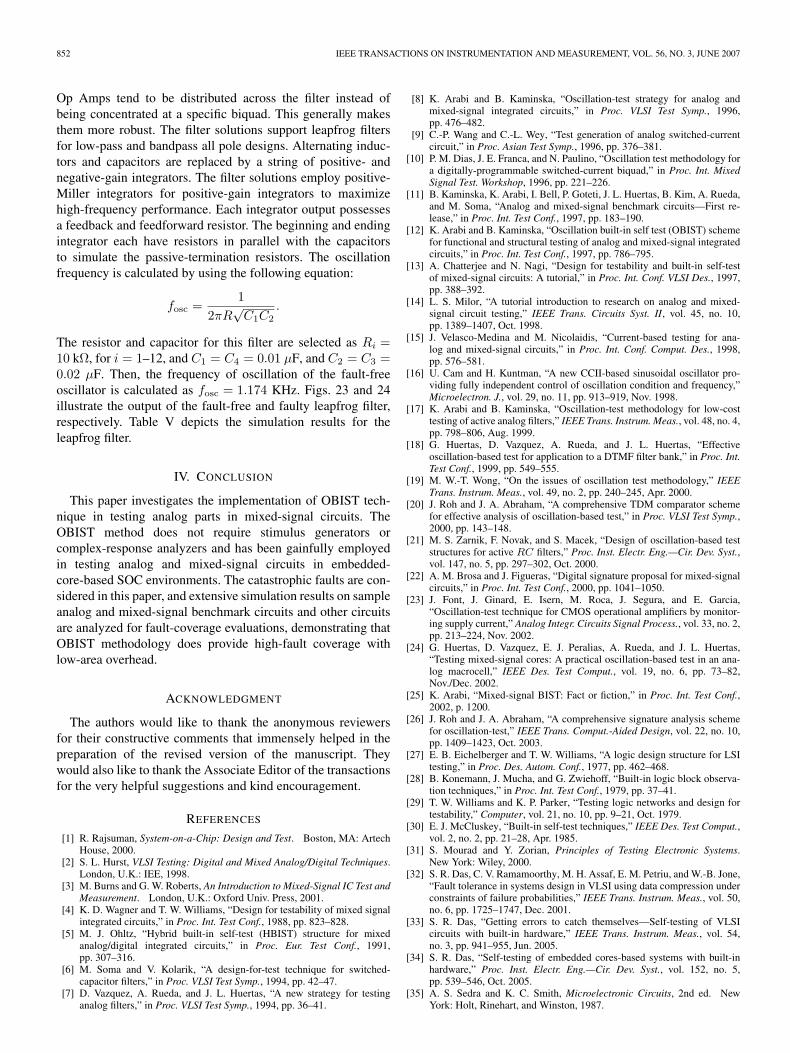
F. Leapfrog Filter
Another circuit used for our test is a leapfrog filter from theanalog and mixed-signal benchmark circuits—first release list[11]. Fig. 22 illustrates the leapfrog-filter circuit. The advantageof this type of filter is that errors due to element values or
852 IEEE TRANSACTIONS ON INSTRUMENTATION AND MEASUREMENT, VOL. 56, NO. 3, JUNE 2007
Op Amps tend to be distributed across the filter instead ofbeing concentrated at a specific biquad. This generally makesthem more robust. The filter solutions support leapfrog filtersfor low-pass and bandpass all pole designs. Alternating induc-tors and capacitors are replaced by a string of positive- andnegative-gain integrators. The filter solutions employ positive-Miller integrators for positive-gain integrators to maximizehigh-frequency performance. Each integrator output possessesa feedback and feedforward resistor. The beginning and endingintegrator each have resistors in parallel with the capacitorsto simulate the passive-termination resistors. The oscillationfrequency is calculated by using the following equation:
fosc =1
2πR√C1C2
.
The resistor and capacitor for this filter are selected as Ri =10 kΩ, for i = 1–12, and C1 = C4 = 0.01 µF, and C2 = C3 =0.02 µF. Then, the frequency of oscillation of the fault-freeoscillator is calculated as fosc = 1.174 KHz. Figs. 23 and 24illustrate the output of the fault-free and faulty leapfrog filter,respectively. Table V depicts the simulation results for theleapfrog filter.
IV. CONCLUSION
This paper investigates the implementation of OBIST tech-nique in testing analog parts in mixed-signal circuits. TheOBIST method does not require stimulus generators orcomplex-response analyzers and has been gainfully employedin testing analog and mixed-signal circuits in embedded-core-based SOC environments. The catastrophic faults are con-sidered in this paper, and extensive simulation results on sampleanalog and mixed-signal benchmark circuits and other circuitsare analyzed for fault-coverage evaluations, demonstrating thatOBIST methodology does provide high-fault coverage withlow-area overhead.
ACKNOWLEDGMENT
The authors would like to thank the anonymous reviewersfor their constructive comments that immensely helped in thepreparation of the revised version of the manuscript. Theywould also like to thank the Associate Editor of the transactionsfor the very helpful suggestions and kind encouragement.
REFERENCES
[1] R. Rajsuman, System-on-a-Chip: Design and Test. Boston, MA: ArtechHouse, 2000.
[2] S. L. Hurst, VLSI Testing: Digital and Mixed Analog/Digital Techniques.London, U.K.: IEE, 1998.
[3] M. Burns and G. W. Roberts, An Introduction to Mixed-Signal IC Test andMeasurement. London, U.K.: Oxford Univ. Press, 2001.
[4] K. D. Wagner and T. W. Williams, “Design for testability of mixed signalintegrated circuits,” in Proc. Int. Test Conf., 1988, pp. 823–828.
[5] M. J. Ohltz, “Hybrid built-in self-test (HBIST) structure for mixedanalog/digital integrated circuits,” in Proc. Eur. Test Conf., 1991,pp. 307–316.
[6] M. Soma and V. Kolarik, “A design-for-test technique for switched-capacitor filters,” in Proc. VLSI Test Symp., 1994, pp. 42–47.
[7] D. Vazquez, A. Rueda, and J. L. Huertas, “A new strategy for testinganalog filters,” in Proc. VLSI Test Symp., 1994, pp. 36–41.
[8] K. Arabi and B. Kaminska, “Oscillation-test strategy for analog andmixed-signal integrated circuits,” in Proc. VLSI Test Symp., 1996,pp. 476–482.
[9] C.-P. Wang and C.-L. Wey, “Test generation of analog switched-currentcircuit,” in Proc. Asian Test Symp., 1996, pp. 376–381.
[10] P. M. Dias, J. E. Franca, and N. Paulino, “Oscillation test methodology fora digitally-programmable switched-current biquad,” in Proc. Int. MixedSignal Test. Workshop, 1996, pp. 221–226.
[11] B. Kaminska, K. Arabi, I. Bell, P. Goteti, J. L. Huertas, B. Kim, A. Rueda,and M. Soma, “Analog and mixed-signal benchmark circuits—First re-lease,” in Proc. Int. Test Conf., 1997, pp. 183–190.
[12] K. Arabi and B. Kaminska, “Oscillation built-in self test (OBIST) schemefor functional and structural testing of analog and mixed-signal integratedcircuits,” in Proc. Int. Test Conf., 1997, pp. 786–795.
[13] A. Chatterjee and N. Nagi, “Design for testability and built-in self-testof mixed-signal circuits: A tutorial,” in Proc. Int. Conf. VLSI Des., 1997,pp. 388–392.
[14] L. S. Milor, “A tutorial introduction to research on analog and mixed-signal circuit testing,” IEEE Trans. Circuits Syst. II, vol. 45, no. 10,pp. 1389–1407, Oct. 1998.
[15] J. Velasco-Medina and M. Nicolaidis, “Current-based testing for ana-log and mixed-signal circuits,” in Proc. Int. Conf. Comput. Des., 1998,pp. 576–581.
[16] U. Cam and H. Kuntman, “A new CCII-based sinusoidal oscillator pro-viding fully independent control of oscillation condition and frequency,”Microelectron. J., vol. 29, no. 11, pp. 913–919, Nov. 1998.
[17] K. Arabi and B. Kaminska, “Oscillation-test methodology for low-costtesting of active analog filters,” IEEE Trans. Instrum. Meas., vol. 48, no. 4,pp. 798–806, Aug. 1999.
[18] G. Huertas, D. Vazquez, A. Rueda, and J. L. Huertas, “Effectiveoscillation-based test for application to a DTMF filter bank,” in Proc. Int.Test Conf., 1999, pp. 549–555.
[19] M. W.-T. Wong, “On the issues of oscillation test methodology,” IEEETrans. Instrum. Meas., vol. 49, no. 2, pp. 240–245, Apr. 2000.
[20] J. Roh and J. A. Abraham, “A comprehensive TDM comparator schemefor effective analysis of oscillation-based test,” in Proc. VLSI Test Symp.,2000, pp. 143–148.
[21] M. S. Zarnik, F. Novak, and S. Macek, “Design of oscillation-based teststructures for active RC filters,” Proc. Inst. Electr. Eng.—Cir. Dev. Syst.,vol. 147, no. 5, pp. 297–302, Oct. 2000.
[22] A. M. Brosa and J. Figueras, “Digital signature proposal for mixed-signalcircuits,” in Proc. Int. Test Conf., 2000, pp. 1041–1050.
[23] J. Font, J. Ginard, E. Isern, M. Roca, J. Segura, and E. Garcia,“Oscillation-test technique for CMOS operational amplifiers by monitor-ing supply current,” Analog Integr. Circuits Signal Process., vol. 33, no. 2,pp. 213–224, Nov. 2002.
[24] G. Huertas, D. Vazquez, E. J. Peralias, A. Rueda, and J. L. Huertas,“Testing mixed-signal cores: A practical oscillation-based test in an ana-log macrocell,” IEEE Des. Test Comput., vol. 19, no. 6, pp. 73–82,Nov./Dec. 2002.
[25] K. Arabi, “Mixed-signal BIST: Fact or fiction,” in Proc. Int. Test Conf.,2002, p. 1200.
[26] J. Roh and J. A. Abraham, “A comprehensive signature analysis schemefor oscillation-test,” IEEE Trans. Comput.-Aided Design, vol. 22, no. 10,pp. 1409–1423, Oct. 2003.
[27] E. B. Eichelberger and T. W. Williams, “A logic design structure for LSItesting,” in Proc. Des. Autom. Conf., 1977, pp. 462–468.
[28] B. Konemann, J. Mucha, and G. Zwiehoff, “Built-in logic block observa-tion techniques,” in Proc. Int. Test Conf., 1979, pp. 37–41.
[29] T. W. Williams and K. P. Parker, “Testing logic networks and design fortestability,” Computer, vol. 21, no. 10, pp. 9–21, Oct. 1979.
[30] E. J. McCluskey, “Built-in self-test techniques,” IEEE Des. Test Comput.,vol. 2, no. 2, pp. 21–28, Apr. 1985.
[31] S. Mourad and Y. Zorian, Principles of Testing Electronic Systems.New York: Wiley, 2000.
[32] S. R. Das, C. V. Ramamoorthy, M. H. Assaf, E. M. Petriu, and W.-B. Jone,“Fault tolerance in systems design in VLSI using data compression underconstraints of failure probabilities,” IEEE Trans. Instrum. Meas., vol. 50,no. 6, pp. 1725–1747, Dec. 2001.
[33] S. R. Das, “Getting errors to catch themselves—Self-testing of VLSIcircuits with built-in hardware,” IEEE Trans. Instrum. Meas., vol. 54,no. 3, pp. 941–955, Jun. 2005.
[34] S. R. Das, “Self-testing of embedded cores-based systems with built-inhardware,” Proc. Inst. Electr. Eng.—Cir. Dev. Syst., vol. 152, no. 5,pp. 539–546, Oct. 2005.
[35] A. S. Sedra and K. C. Smith, Microelectronic Circuits, 2nd ed. NewYork: Holt, Rinehart, and Winston, 1987.

DAS et al.: TESTING ANALOG AND MIXED-SIGNAL CIRCUITS WITH BUILT-IN HARDWARE—A NEW APPROACH 853
Sunil R. Das (M’70–SM’90–F’94–LF’04) receivedthe B.Sc. degree (with honors) in physics and theM.Sc. (Tech.) and Ph.D. degrees in radiophysicsand electronics from the University of Calcutta,Calcutta, West Bengal, India.
He previously held academic and research posi-tions with the Department of Electrical Engineeringand Computer Sciences, Computer Science Division,University of California, Berkeley; the Center forReliable Computing, Computer Systems Laboratory,Department of Electrical Engineering, Stanford Uni-
versity, Stanford, CA (on sabbatical leave); the Institute of Computer Engineer-ing, National Chiao Tung University, Hsinchu, Taiwan, R.O.C.; and the Centerof Advanced Study, Institute of Radiophysics and Electronics, University ofCalcutta. He is currently an Emeritus Professor of electrical and computerengineering in the School of Information Technology and Engineering, Uni-versity of Ottawa, Ottawa, ON, Canada, and is also currently a Professor ofcomputer and information science, Troy University, Montgomery, AL. He haspublished around 300 papers in the areas of switching and automata theory,digital logic design, threshold logic, fault-tolerant computing, built-in self-testwith emphasis on embedded cores-based system-on-chip, microprogrammingand microarchitecture, microcode optimization, applied theory of graphs, andcombinatorics.
Dr. Das has served in the Technical Program Committees and OrganizingCommittees of many IEEE and non-IEEE International Conferences, Sym-posia, and Workshops and has also acted as session organizer, session chair,and panelist. He was elected one of the delegates of the prestigious GOODPEOPLE, GOOD DEEDS of the Republic of China in 1981 in recognitionof his outstanding contributions in the field of research and education. He islisted in the MARQUIS WHO’S WHO Biographical Directory of the ComputerGraphics Industry, Chicago, IL (first edition, 1984). He served as the ManagingEditor of the IEEE Very Large-Scale Integration (VLSI) Technical Bulletin,which is a publication of the IEEE Computer Society Technical Committee(TC) on VLSI since its very inception, and was also an Executive CommitteeMember of the IEEE Computer Society TC on VLSI. He has also servedas an Associate Editor of the IEEE TRANSACTIONS ON SYSTEMS, MAN,AND CYBERNETICS (subsequently, Parts A, B, and C) since 1991 until veryrecently. He is currently an Associate Editor of the IEEE TRANSACTIONS
ON INSTRUMENTATION AND MEASUREMENT; an Associate Editor of theInternational Journal of Computers and Applications published by Acta Press,Calgary, AB; a Regional Editor for the Information Technology Journal,which is an official publication of an Asian Network for Scientific Information;and a former member of the Editorial Board and a Regional Editor forCanada of VLSI Design: An International Journal of Custom-Chip Design,Simulation, and Testing published by Gordon and Breach Science Publishers,Inc., NY. He is a former Administrative Committee Member of the IEEESystems, Man, and Cybernetics Society, a former Associate Editor of the IEEETRANSACTIONS ON VERY LARGE-SCALE INTEGRATION (VLSI) SYSTEMS
(for two consecutive terms), a former Associate Editor of the Special InterestGroup on Design Automation (SIGDA) Newsletter, which is the publication ofthe Association for Computing Machinery (ACM) Special Interest Group onDesign Automation, a former Associate Editor of the International Journal ofComputer Aided VLSI Design published by Ablex, Norwood, NJ, and a formerAssociate Editor of the International Journal of Parallel and DistributedSystems and Networks published by Acta Press. He also served as the Cochairof the IEEE Computer Society Students Activities Committee from Region 7(Canada). He was the Associate Guest Editor of the IEEE JOURNAL OF
SOLID-STATE CIRCUITS Special Issues on Microelectronic Systems (thirdand fourth Special Issues) and Guest Editor of the International Journal ofComputer Aided VLSI Design (September 1991), as well as VLSI Design: AnInternational Journal of Custom-Chip Design, Simulation, and Testing (March1993, September 1996, and December 2001), Special Issues on VLSI Testing.He also Guest Edited, jointly with R. Rajsuman, Special Sections of the IEEETRANSACTIONS ON INSTRUMENTATION AND MEASUREMENT in the area ofVLSI Testing, first in October 2003 (Innovations in VLSI Test Equipments),and then in October 2005 and April 2006 (Future of Semiconductor Test). Heis the founding Editor-in-Chief of the International Journal of Computers,Information Technology and Engineering being published by Serials Publi-cations, Delhi, India. He edited, jointly with P. K. Srimani, a book entitled,Distributed Mutual Exclusion Algorithms (IEEE Computer Society Press, LosAlamitos, CA, 1992) in its Technology Series. He is also the author, jointly withC. L. Sheng, of a text on Digital Logic Design to be published by Ablex. He is amember of the IEEE Computer Society, IEEE Systems, Man, and CyberneticsSociety, IEEE Circuits and Systems Society, and IEEE Instrumentation andMeasurement Society, and a member of the ACM, USA. He was elected aFellow of the IEEE in 1994 for contributions to switching theory and com-puter design. He was the recipient of the 1996 IEEE Computer Society’s highly
esteemed Technical Achievement Award for his pioneering contributions inthe fields of switching theory and modern digital design, digital circuitstesting, microarchitecture and microprogram optimization, and combina-torics and graph theory. He was also the recipient of the 1997 IEEE ComputerSociety’s Meritorious Service Award for excellent service contributions toIEEE TRANSACTIONS ON VERY LARGE-SCALE INTEGRATION (VLSI)SYSTEMS and the Society and was elected a Fellow of the Society for Designand Process Science, USA, in 1998 for his accomplishments in integration ofdisciplines, theories, and methodologies, development of scientific princi-ples and methods for design and process science as applied to traditionaldisciplines of engineering, industrial leadership and innovation, and edu-cational leadership and creativity. In recognition as one of the distinguishedcore of dedicated volunteers and staff whose leadership and services madethe IEEE Computer Society the world’s preeminent association of computingprofessionals, he was made a Golden Core Member of the Computer Societyin 1998. Besides, he was the recipient of the IEEE Circuit and SystemsSociety’s Certificates of Appreciation for services rendered as AssociateEditor, IEEE TRANSACTIONS ON VERY LARGE-SCALE INTEGRATIONSYSTEMS, during 1995–1996 and 1997–1998, and of the IEEE ComputerSociety’s Certificates of Appreciation for services rendered to the Societyas Member of the Society’s Fellow Evaluation Committee, once in 1998 andthen in 1999. He served as a member of the IEEE Computer Society’s FellowEvaluation Committee for 2001 and 2005–2007 as well. He was elected aFellow of the Canadian Academy of Engineering in 2002 for pioneeringcontributions to computer engineering research—specifically in the fieldsof switching theory and computer design, fault-tolerant computing, mi-croarchitecture and microprogram optimization, and to some problemareas in applied theory of graphs and combinatorics. He was elected aFellow of the Engineering Institute of Canada in 2005 for exceptional con-tributions to Engineering in Canada. He was the recipient of the prestigiousRudolph Christian Karl Diesel Best Paper Award of the Society for Designand Process Science in recognition of the excellence of his paper presentedat the Fifth Biennial World Conference on Integrated Design and ProcessTechnology held in Dallas, TX, on June 4–8, 2000. He was also the corecipientof the IEEE’s esteemed Donald G. Fink Prize Paper Award for 2003 forhis paper published in the December 2001 issue of the IEEE TRANSACTIONS
ON INSTRUMENTATION AND MEASUREMENT. He is the 2007 recipient of theprestigious C. V. Ramamoorthy Distinguished Scholar Award of the Societyfor Design and Process Science for his significant achievement through researchin the field of design and process science.
Jila Zakizadeh received the B.Sc. degree in elec-tronics engineering from Shahid Bahonar University,Kerman, Iran, in 1992 and the M.Sc. degree insystems science from University of Ottawa, Ottawa,ON, Canada in 2005.
She is now with the Faculty of Engineering,School of Information Technology and Engineering,University of Ottawa, as a part-time researcher. Herresearch interests include mixed-signal IC test, built-in self-test, and embedded systems design.

854 IEEE TRANSACTIONS ON INSTRUMENTATION AND MEASUREMENT, VOL. 56, NO. 3, JUNE 2007
Satyendra Biswas (M’98) received the B.Sc. de-gree in electrical and electronic engineering fromBangladesh University of Engineering and Technol-ogy, Dhaka, Bangladesh, in 1991 and the M.Sc.degree in electrical and electronic engineering andthe Ph.D. degree in systems engineering fromYamaguchi University, Yamaguchi, Japan, in 1996and 1999, respectively.
He was an R&D Engineer for Nippon TelevisionCompany, Dhaka, and with General Cybernetics Inc.,Toronto, ON, Canada. From 2003 to 2005, he was a
Research Assistant at the University of Ottawa, Ottawa, ON. He is currentlyan Assistant Professor of electrical engineering and technology at GeorgiaSouthern University, Statesboro. He has published several technical papersin journals and presented at international conferences. His current researchinterests include very large-scale integration circuit design and testing, datacompression in built-in self-testing, dynamic image/video processing, andreconfigurable computing.
Dr. Biswas is a registered Professional Engineer (P.Eng.) and a member ofthe Institute of Electronics, Information, and Communication Engineers.
Mansour H. Assaf (M’02) received the degree (withhonors) in applied physics from the Lebanese Uni-versity, Beirut, Lebanon, in 1989 and the B.A.Sc.,M.A.Sc., and Ph.D. degrees in electrical and com-puter engineering from the University of Ottawa,Ottawa, ON, Canada, in 1994, 1996, and 2003,respectively.
From 2003 to 2006, he was associated with theSensing and Modeling Research Laboratory of theUniversity of Ottawa as a Research Fellow. He iscurrently an Assistant Professor of information tech-
nology and computer engineering at the University of Trinidad and Tobago,Arima. His research interests include computer architecture, computer net-works, fault-tolerant computing, and fault diagnosis in mixed-signal systems,including system-on-chip design and test. He has published 12 journal papersand over 20 conference articles.
Dr. Assaf is a member of the IEEE Computer Society and of theCanadian Mathematical Society. He served as a session Cochair member ona number of international conferences on computing techniques and has been areviewer of several internationally known journals and conferences such as theIEEE TRANSACTIONS ON INSTRUMENTATION AND MEASUREMENT, the In-ternational Association of Science and Technology for Development (IASTED)Journal of Computers and Applications, and the World Multi-Conference onSystemics, Cybernetics, and Informatics (WMSCI).
Amiya R. Nayak (M’86–SM’03) received theB.Math. degree in computer science and com-binatorics and optimization from University ofWaterloo, Waterloo, ON, Canada, in 1981 and thePh.D. degree in systems and computer engineeringfrom Carleton University, Ottawa, ON, in 1991.
He has over 17 years of industrial experience,working at CMC Electronics (formerly known asCanadian Marconi Company), Defence ResearchEstablishment Ottawa, EER Systems, and NortelNetworks, in software engineering, avionics, and
navigation systems, simulation, and system-level performance analysis. Since1994, he has been an Adjunct Research Professor in the School of ComputerScience at Carleton University. Currently, he is a Full Professor at the School ofInformation Technology and Engineering, University of Ottawa. His researchinterests are in the area of fault tolerance, distributed systems/algorithms, andmobile ad hoc network with over 90 publications in refereed journals andconference proceedings.
Dr. Nayak was the Book Review and Canadian Editor of Very Large-ScaleIntegration Design from 1996 to 2002. He is on the Editorial Board of theInternational Journal of Parallel, Emergent, and Distributed Systems, andAssociate Editor of the International Journal of Computing and InformationScience.
Emil M. Petriu (M’86–SM’88–F’01) is a Professorwith the School of Information Technology andEngineering, University of Ottawa, Ottawa, ON,Canada, where he has been since 1985. His researchinterests include test and measurement systems, in-teractive virtual environments, intelligent sensors,robot sensing and perception, neural networks, andfuzzy control. During his career, he has publishedmore than 200 technical papers, authored two books,edited another two books, and is the holder oftwo patents.
Dr. Petriu is a Fellow of the Canadian Academy of Engineering andFellow of the Engineering Institute of Canada. He was the corecipient ofthe IEEE’s Donald G. Fink Prize Paper Award for 2003 and the 2003 IEEEInstrumentation and Measurement Society Award. He is currently serving as amember of the ADCOM and Chair of TC-15—Virtual Systems and Cochair ofTC-28—Instrumentation and Measurement for Robotics and Automation andTC-30—Security and Contraband Detection of the IEEE Instrumentation andMeasurement Society. He is an Associate Editor of the IEEE TRANSACTIONS
ON INSTRUMENTATION AND MEASUREMENT and member of the EditorialBoard of the IEEE I&M Magazine.
Wen-Ben Jone (S’85–M’88–SM’01) was born inTaipei, Taiwan, R.O.C. He received the B.S. degreein computer science and the M.S. degree in com-puter engineering from National Chiao-Tung Univer-sity, Hsin-Chu, Taiwan, in 1979 and 1981, respec-tively, and the Ph.D. degree in computer engineeringand science from Case Western Reserve University,Cleveland, OH, in 1987.
In 1987, he was with the Department of ComputerScience at the New Mexico Institute of Mining andTechnology, Socorro, where he was promoted to
Associate Professor in 1992. From 1993 to 2000, he was with the Departmentof Computer Engineering and Information Science, National Chung-ChengUniversity, Chiayi, Taiwan. He was a Visiting Research Fellow with theDepartment of Computer Science and Engineering, the Chinese Universityof Hong Kong, in the summer of 1997. From 2001, he has been with theDepartment of Electrical and Computer Engineering and Computer Science,University of Cincinnati, Cincinnati, OH. He was a Visiting Scholar with theInstitute of Information Science, Academia Sinica, Taiwan in the summer of2002. His research interests include very large-scale integration (VLSI) designfor testability, built-in self-testing, memory testing, high-performance circuittesting, MEMS testing and repairing, and low-power circuit design and test. Hehas published more than 100 papers and is the holder of one U.S. patent.
Dr. Jone served as a Reviewer in these research areas in various technicaljournals and conferences. He is also listed in the Marquis Who’s Who in theWorld (15th Edition, 1998, 2001). He also served on the program committeeof the VLSI Design/CAD Symposium (1993–1997, in Taiwan, R.O.C.). Hewas the General Chair of 1998 VLSI Design/CAD Symposium, served onthe program committee of the 1995, 1996, and 2000 Asian Test Conference,the 1995–1998 Asia and South Pacific Design Automation Conference, the1998 International Conference on Chip Technology, the 2000 InternationalSymposium on Defect and Fault Tolerance in VLSI Systems, and the 2002 and2003 Great Lakes Symposium on VLSI. He was the recipient of the Best ThesisAward from The Chinese Institute of Electrical Engineering, China, in 1981. Hewas the corecipient of the 2003 IEEE Donald G. Fink Prize Paper Award. He is amember of the IEEE Computer Society Test Technology Technical Committee.

DAS et al.: TESTING ANALOG AND MIXED-SIGNAL CIRCUITS WITH BUILT-IN HARDWARE—A NEW APPROACH 855
Mehmet Sahinoglu (S’78–M’81–SM’93) receivedthe B.S. degree in electrical engineering from MiddleEast Technical University (METU), Ankara, Turkey,and the M.S. degree in electrical engineering fromthe University of Manchester Institute of Science andTechnology (UMIST), Manchester, U.K., and thePh.D. degree in statistics and electrical engineeringfrom Texas A&M University, College Station.
He originated, jointly with D. Libby, the“Sahinoglu–Libby (SL) pdf” in 1981, “CompoundPoisson Software Reliability Model” in 1992, and
“Compound Poisson Stopping Rule Algorithm” in 1997 in cost-effective soft-ware testing and, recently, “The Security-Meter” in 2005 to quantify risk.He is currently researching the reliability, security, and privacy modelingof hardware and software systems and writing a text book on TrustworthyComputing Concepts (TWC). He is a 2006 Microsoft Research Scholar of TWCCurriculum: one of 14 awardees around the globe. He has written 25 journalpapers, nearly 100 refereed proceedings and technical reports, and has beenthe Principal Investigator of ten national (in Turkey) and seven international(United Nations, Economic Commission of Europe, and USA) technical grantson the subject of system reliability and security. He is a published author ofthree creative (social and travel memoirs) books in Turkish and two technicalbooks (class notes on random-number generation/simulation and stochasticprocesses in English) and will be publishing his new book entitled Trustwor-thy Computing: Analytical and Quantitative Engineering Evaluation with aCD-ROM: T∗Solver, all in June 2007 by Wiley and Sons. He has organizedthe two-week long International Summer School of ISI-IASC Design of Ex-periments on Reliability Engineering in Izmir/Turkey in 1995 while serving asthe Dean of Science in Izmir’s Dokuz Eylul University (DEU). He formallyretired from METU and DEU, jointly in 2000, after 26.5 years of service to theuniversities and the Turkish Electricity Authority (TEK) in Turkey. He has beenan Invited Speaker internationally in Japan, China, Brazil, Australia, and USAand has appeared in NPR interviews in USA and nationally televised culturaltalk programs in Turkey. Since 2000, he has been organizing the Troy Univer-sity, Montgomery Millennium’s Honorary IT Speakers’ Colloquium Series forthe area IT students and corporations. Currently, he holds the Eminent Scholarposition of the Alabama Commission on Higher Education (ACHE) and isserving as the Head of the School of Computer Science at Montgomery campusof the Troy University located at the Gunter/Maxwell AFB, Montgomery, AL.
Dr. Sahinoglu is a Fellow of the Society for Design and Process Science anda member of the Armed Forces Communications and Electronics Association(AFCEA), the Association for Computing Machinery, and the ASA, and is anelected member of ISI, IASC, and the Turkish Institute of Statistics.