system nintendo entertainment - rochester institute...
TRANSCRIPT

Now you’re playing with power!
Nintendo Entertainment System
Seth Hendrick, Alex Sarra
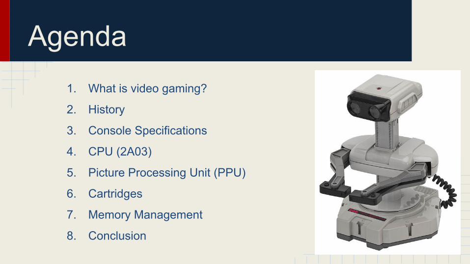
Agenda1. What is video gaming?
2. History
3. Console Specifications
4. CPU (2A03)
5. Picture Processing Unit (PPU)
6. Cartridges
7. Memory Management
8. Conclusion

What is video gaming?● Popular pastime of today’s youth, and other’s not so youthful● Video gamers
○ Excited about gaming○ Want to see continual progress
● Market○ Several competing companies○ Satisfy gamer’s needs○ Nintendo, Sony, Microsoft, etc.○ Strategy is different based on company
● Nintendo○ Hardware is traditionally less expensive○ Cost is generally lower per console unit with higher
market longevity

History● Nintendo released the FAMICOM (FAMily COMputer) in Japan in 1984 [2]
● Despite the video game crash in the US, Nintendo released the N.E.S. in 1986.
○ $250 version came with R.O.B., Gyromite, Super Mario Bros, 2 controllers,
Duck Hunt, and a light gun
○ $200 version came with Super Mario Bros, and 2 controllers.
● Nintendo designed the N.E.S. to look like a VCR instead of a Video Game System due to the crash.

History● 1993: Nintendo released the N.E.S. 2
● 1995: Nintendo discontinued the N.E.S.
● The N.E.S. sold 62 million systems and over 500 million games
○ One of the most popular game systems of all time.
NES 2 - 1993 ReleaseNES External Design

Console Specifications● 8-bit CPU● 1.79 MHz● PPU● 64 Value Color Palette● System Memory - 2KB● VRAM - 2KB● Program ROM - 32+ KB● Character ROM - 8+ KB● Sprite RAM - 256 Bytes● Temporary Sprite RAM - 24 bytes● Color palette RAM - 32 bytes [4]


CPU - 2A03Overview [2 ,p.9]:● Ricoh - 2A03● NMOS● Little Endian● 8-bit data bus● MMC● 8-bit control● 16-bit address
Processor Diagram

CPU - 2A03Memory Access [2 ,pp. 9,10]:● ROM
○ Read-only○ Accessed via MMC
● MMC○ Controller for ROM access○ Allows for bank swapping
● RAM○ Mirroring○ Zero Page○ PRG-ROM
● Address Bus○ 16-bit○ Set address○ Support for 64KB
■ $0000-$FFFF● Control Bus
○ Read or Write?○ Screen Mirroring○ Disk IRQs
● I/O○ PPU and control

CPU - 2A03 - Registers● Registers [2, pp. 11-13]
○ 16 - bit Program Counter (PC)
■ Games could only be 64 Kb
○ 8 - bit Stack Pointer (SP)
○ 8 - bit Accumulator (A)
○ 8 - bit Index Register X (X)
○ 8 - bit Index Register Y (Y)
● 8 - bit Processor Status○ N - is number negative○ V - overflow○ B - set if the BRK instruction
occurs○ D - Used to switch into BCD
mode○ I - Disable interrupts○ Z - Zero○ C - Carry

CPU - 2A03 - ISA● Instruction Set Architecture [8]
○ Load/Store operations■ LDA, LDX, LDY, STA, STX, STY, etc.
○ Register Transfer Operations■ TAX, TAY, TSX, TXA, TXY, etc.
○ Stack Operations■ PHA, PLA, etc.
○ Arithmetic Operations■ ADC, AND, etc.
○ Increments / Decrements■ INX, INY, DEX, DEY, etc.
● Shifts○ ASL, LSR
● Jumps/calls○ JMP, JSR
● Branches○ BNE, BEQ
● Status Register Operations○ CLC, CLI, SEC, SEI

Picture Processing Unit (PPU)● The CPU by itself was not enough power [3]● The Picture Processing unit could:
○ Generate Colors○ Move characters on the Screen○ Display 52 colors
■ 24 allowed on the screen at the same time■ Other video game units only had 6-8 colors.

Picture Processing Unit (PPU)Memory Map [2, p. 17]● Pattern Tables● Name Tables● Palettes● Mirrors

Picture Processing Unit (PPU)Pattern Tables [3]● The sprites and background images are saved in here● Sprites are 8X8 pixel titles
○ Titles are 16 bytes (128 bits)○ Each byte (bits) is a row in the sprite○ The sprites have 2 layers
■ First 8 bytes are the first layer■ Second 8 bytes are the second layer
○ Each sprite can have 4 possible colors

Picture Processing Unit (PPU)
Layer 2 Layer 1 Overall Palette Assignment0 0 00 Color 00 1 01 Color 11 0 10 Color 21 1 11 Color 3
Layer 1
Layer 2
Combined
Images from Badder Hacks
Picture Processing Unit (PPU)Name Tables [3]● Backgrounds are stored here● PPU supports 4 name tables● NES RAM can only support 2
○ Other 2 tables are mirrored● Each table has 30, 32-byte strings of data
○ tiles assigned left-to-right, top-to-bottom● Remaining 64 bytes are for background palette assignments

Picture Processing Unit (PPU)● Scrolling with nametables [3]
Image from Badder Hacks Image from NES System Documentation

Picture Processing Unit (PPU)Palettes [3]● Consists of four colors chosen from NES’ internal index● Tiles are colored by assigning them a palette● Background tiles can be assigned to any of four palettes● Sprite tiles can be assigned to any of a separate set of four palettes
Layer 2 Layer 1 Overall Palette Assignment0 0 00 Color 00 1 01 Color 11 0 10 Color 21 1 11 Color 3
Image from NES System Documentation

Cartridges● Unlike previous systems, Nintendo released a cartridge standard.● The FAMICOM cartridge
○ Smaller than the N.E.S. Cartridge○ 60 pin connection
● The N.E.S. Cartridge○ Bigger than the FAMICOM’s○ 72 - pin connection○ Mostly empty space○ Had a “Lock out system.”
● The N.E.S. had enough memory for early games○ Some games needed more○ Cartridges could have their own ROM.
Images from NES System Documentation

Memory Management● Game Specific MMC [6]
○ Nintendo made 9○ Konami made 4○ Namco○ Sunsoft
● Supplement On-Board MMC○ More complexity → Increasing demand○ Swappable memory
Konami VRC4
Nintendo MMC3

Memory Management● How Memory Mapping works [6]:
○ The N.E.S. used bank switching○ MMC monitors memory writes for specific address (or range)○ When the system needs access to data on a ROM bank and
the data is not in PRG-ROM yet, software indicates the need to switch banks.
○ The selected memory is loaded into the bank in PRG-ROM from the cartridge.
● The use of memory mappers helped the N.E.S. to survive technological limitations and extend the life of their product

Conclusion● The NES uses the 6502 Microprocessor
● The NES has its own custom PPU
● The NES can swap memory between it and the cartridge
● The NES was one of the most popular Video Game Systems
● The Super NES was the NES’s replacement (1990 Japan, 1991
US).
● Nintendo continues to follow practices regarding selling their
consoles that started with the NES today.

THANK YOU!Any Questions, Comments, Queries, or Threats?

References[1] ClassicGaming Museum. Nintendo Entertainment System [Online]. Available: http://classicgaming.gamespy.com/View.php?view=ConsoleMuseum.Detail&id=26&game=5[2] P. Dishkin. (2004, August). Nintendo Entertainment System Documentation [Online]. Available: http://nesdev.com/NESDoc.pdf[3] D. Floppy. (2011, May 24). The NES Picture Processing Unit [Online]. Available: http://badderhacksnet.ipage.com/badderhacks/index.php?option=com_content&view=article&id=270:the-nes-picture-processing-unit-ppu&catid=14:dr-floppy&Itemid=7[4] J. Downey and L. Kauppila et al., (2004, December 9). The Design and Implementation of the Nintendo Entertainment System [Online]. Available: http://web.mit.edu/6.111/www/f2004/projects/dkm_report.pdf[5] NESWORLD. The Nintendo Entertainment System [Online]. Available: http://www.nesworld.com/nes.php[6] Wikipedia. Memory Management Controller [Online]. Available: http://en.wikipedia.org/wiki/Memory_management_controller[7] Wikipedia. Nintendo Entertainment System [Online]. Available: http://en.wikipedia.org/wiki/Nintendo_Entertainment_System[8] 6502 Microprocessor [Online]. Available: http://emu-docs.org/CPU%2065xx/6502.txt