synthesis based introduction to opamps and phase …nagendra/papers/isc12-opamppllsynth-sl.pdf ·...
TRANSCRIPT
Synthesis Based Introduction to Opamps and
Phase Locked Loops
2012 International Symposium on Circuits and Systems
Seoul, Korea
Nagendra Krishnapura
Department of Electrical EngineeringIndian Institute of Technology, Madras
Chennai, 600036, India
23 May 2012
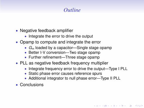
Outline
• Negative feedback amplifier
• Integrate the error to drive the output
• Opamp to compute and integrate the error
• Gm loaded by a capacitor—Single stage opamp• Better I-V conversion—Two stage opamp• Further refinement—Three stage opamp
• PLL as negative feedback frequency multiplier
• Integrate frequency error to drive the output—Type I PLL• Static phase error causes reference spurs• Additional integrator to null phase error—Type II PLL
• Conclusions

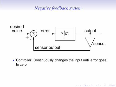
Negative feedback system
controllerΣ
sensor output
outputerrorvalue
-+sensor
desired
• Controller: Continuously changes the input until error goes
to zero
Negative feedback system
Σ
sensor output
outputerror
-+sensor
γ dtvalue
desired
• Controller: Continuously changes the input until error goes
to zero
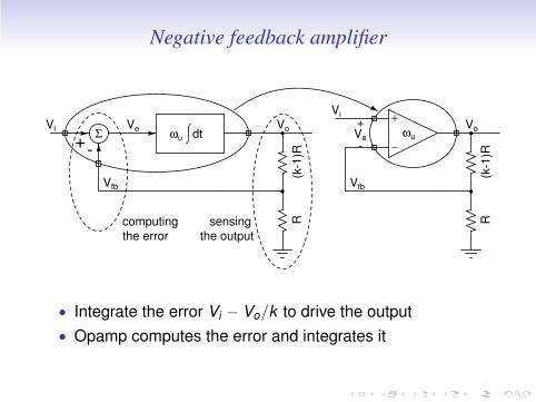
Negative feedback amplifier
ΣVo
-+Vi
Vfb
Veωu dt
−
+
Ve
+
-
Vi
Vo
Vfb
(k-1
)R
ωu
sensing
the output
computing
the error
RR(k
-1)R
• Integrate the error Vi − Vo/k to drive the output
• Opamp computes the error and integrates it
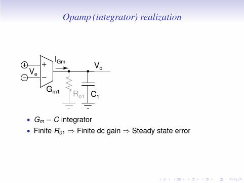
Opamp (integrator) realization
−
+
C1
Gm1 Ro1
IGmVo
Ve
• Gm − C integrator
• Finite Ro1 ⇒ Finite dc gain ⇒ Steady state error
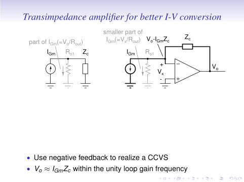
Transimpedance amplifier for better I-V conversion
IGm ZcRo1
part of IGm(=Vo/Rout)
Vo
Vo-IGmZc
−
+
Zc
+
-
Vx
IGm Ro1
smaller part of
IGm(=Vx/Rout)
• Use negative feedback to realize a CCVS
• Vo ≈ IGmZc within the unity loop gain frequency

Improved I-V conversion—Two stage opamp
IGm ZcRo1
Gm1
C1
IGm
−
+
Gm2C2
part of IGm(=Vo/Rout)
single stage opamp
synthesized earlier
Ro1Ro2
Vo
Vo
Vo-IGmZc
−
+
Zc
+
-
Vxωu
IGm Ro1
smaller part of
IGm(=Vx/Rout)
Ve
−
+
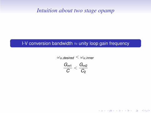
Intuition about two stage opamp
I-V conversion bandwidth ≈ unity loop gain frequency
ωu,desired < ωu,inner
Gm1
C<Gm2
C2
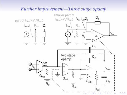
Further improvement—Three stage opamp
−
+
Gm2
C2
−
+
Gm3 C3
C1
Vout
two stage
Ro3
Ro2
Gm1
IGm
Ro1
opamp
IGm ZcRo1
part of IGm(=Vo/Rout)
Vo
Vo-IGmZc
−
+
Zc
+
-
Vxωu
IGm Ro1
smaller part of
IGm(=Vx/Rout)
Ve
−
+
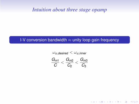
Intuition about three stage opamp
I-V conversion bandwidth ≈ unity loop gain frequency
ωu,desired < ωu,inner
Gm1
C<Gm2
C2<Gm3
C3

Analysis of two and three stage opamps
• Two stage opamp
• DC gain• Pole locations, pole splitting• Stability constraints• RHP zero and its cancellation
• Three stage opamp
• DC gain• Pole locations• Stability constraints• Zero pair and their optimization
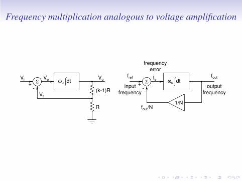
Frequency multiplication analogous to voltage amplification
Σ+-
ωu dt
(k-1)R
R
Vi Vo
Vf
VeΣ+
-
ωu dtfe
input
frequency
fref
output
frequency
fout
fout/N
frequency
error
1/N

Frequency multiplication
Σ
Vctlfref
fout/N
+-
zero, at steady state
Nfrequency
measure
frequency
measure
frequency difference
frequency
divider
γ dt
input
signal
at fref
outputsignalat fout
fout = ffree+KvcoVctl
VCO
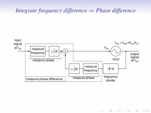
Integrate frequency difference⇒ Phase difference
Σ
Vctl
+-
N
frequency
measure
signal
at fref
output
at foutVCO
frequency
divider
measure
frequency
measure phase
measure phasemeasure phase difference
γ dt
γ dt
input
signal
fout = ffree+KvcoVctl

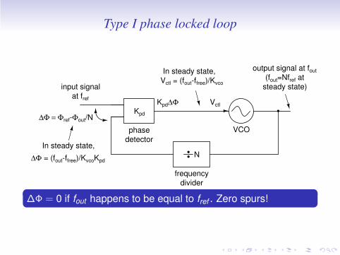
Type I phase locked loop
Vctl
N
output signal
at fout
frequency
divider
input signal at frefphase
detector
fout = ffree+KvcoVctl
VCO
• Phase detector and VCO in a loop
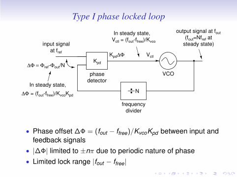
Type I phase locked loop
N
frequency
input signal
at fref
VCO
Kpd
Kpd∆Φ
phase
detector
Vctl = (fout-ffree)/Kvco
Vctl
In steady state, output signal at fout
(fout=Nfref at
steady state)
divider
In steady state,
∆Φ = (fout-ffree)/KvcoKpd
∆Φ = Φref-Φout/N
• Phase offset ∆Φ = (fout − ffree)/KvcoKpd between input and
feedback signals
• |∆Φ| limited to ±nπ due to periodic nature of phase
• Limited lock range |fout − ffree|
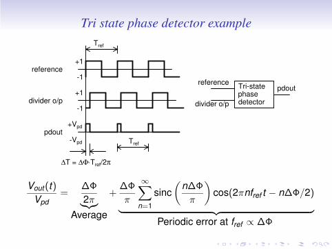
Tri state phase detector example
+1
-1reference
divider o/p divider o/p
referencepdout
pdout
Tref
Tref
Tri-statephasedetector
-Vpd
+Vpd
-1
+1
∆T = ∆Φ⋅Tref/2π
Vout(t)
Vpd=
∆Φ
2π︸︷︷︸
Average
+∆Φ
π
∞∑
n=1
sinc
(n∆Φ
π
)
cos(2πnfref t − n∆Φ/2)
︸ ︷︷ ︸
Periodic error at fref ∝ ∆Φ
Type I PLL with a practical phase detector
• Output average value ∝ ∆Φ
• Periodic signal at fref
• Periodic signal magnitude proportional to ∆Φ
• VCO modulated at fref and its harmonics
• PLL output has sidebands at integer multiples of fref
For a modest sideband level of −40 dB, PLL lock range
≈ 10−4fref . Cannot change N at all!
Type I phase locked loop
N
frequency
input signal
at fref
VCO
Kpd
Kpd∆Φ
phase
detector
Vctl = (fout-ffree)/Kvco
Vctl
In steady state, output signal at fout
(fout=Nfref at
steady state)
divider
In steady state,
∆Φ = (fout-ffree)/KvcoKpd
∆Φ = Φref-Φout/N
∆Φ = 0 if fout happens to be equal to fref . Zero spurs!

Changing the free running frequency of a VCO
(ffree+KvcoVoff)+KvcoVctl ffree’+KvcoVctlVctl
ffree’ = ffree+KvcoVoff
Σ
Voff
Vctl
VCOVCO
• Add a bias to the input to change the free running
frequency
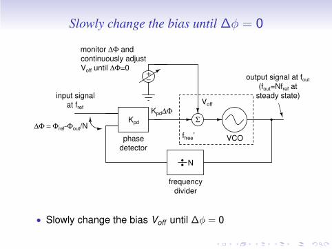
Slowly change the bias until ∆φ = 0
+−
continuously adjust
Voff until ∆Φ=0
N
frequency
input signal
at fref
Σ
Voff
∆Φ = Φref-Φout/NKpd
Kpd∆Φ
phase
detector
divider
VCO
output signal at fout
(fout=Nfref at
steady state)
monitor ∆Φ and
ffree’
• Slowly change the bias Voff until ∆φ = 0
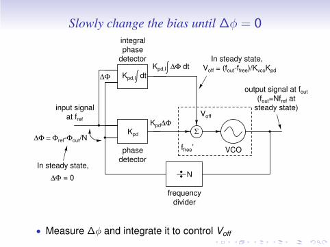
Slowly change the bias until ∆φ = 0
N
frequency
input signal
at fref
Σ
Voff
Kpd
Kpd∆Φ
∆Φ Kpd,I dt
Kpd,I ∆Φ dt
phase
detector
divider
In steady state,
∆Φ = 0
Voff = (fout-ffree)/KvcoKpd
In steady state,
VCO
output signal at fout
(fout=Nfref at
steady state)
ffree’
phase
detector
integral
∆Φ = Φref-Φout/N
• Measure ∆φ and integrate it to control Voff

Type II Phase locked loop
N
input signal
at fref
ΣKpd
Kpd∆Φ
∆Φ Kpd,I dt
Kpd,I ∆Φ dt
In steady state,
∆Φ = 0
VCO
output signal at fout
(fout=Nfref at
steady state)
phase
detector
integral
∆Φ = Φref-Φout/N
phase
detector
proportional
phase detector + loop filter
• Proportional + integral loop filter
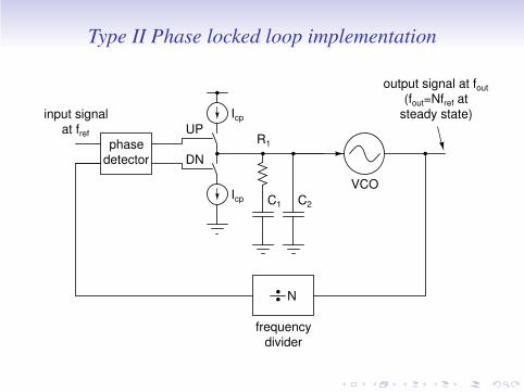
Type II Phase locked loop implementation
phase
detector
Icp
Icp
UP
DN
VCO
output signal at fout
(fout=Nfref at
steady state)
N
input signal
at fref
frequency
divider
R1
C1 C2
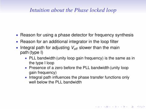
Intuition about the Phase locked loop
• Reason for using a phase detector for frequency synthesis
• Reason for an additional integrator in the loop filter
• Integral path for adjusting Voff slower than the mainpath (type I)
• PLL bandwidth (unity loop gain frequency) is the same as in
the type I loop• Presence of a zero before the PLL bandwidth (unity loop
gain frequency)• Integral path influences the phase transfer functions only
well below the PLL bandwidth
Analysis of type II Phase locked loop
• Pole zero locations
• Phase (jitter) transfer functions
• Higher order loop filter for higher spur suppression

Suggested course outline
• Negative feedback circuits
• Stability analysis
• Opamp topologies using controlled sources (Gm)
• Opamp topologies at the transistor level
• Phase locked loop at the system level

Conclusions
• Negative feedback: Continuous adjustment to reduce error
• Integrator is the key element of the negative feedback loop
• Implementing a voltage integrator and seeking to improve
its performance leads to commonly used opamp topologies
• Implementing a negative feedback frequency multiplier and
seeking to improve its performance leads to type I and II
phase locked loops
• Valuable intuition gained before embarking on analysis
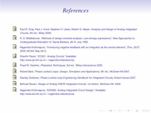
References
Paul R. Gray, Paul J. Hurst, Stephen H. Lewis, Robert G. Meyer, Analysis and Design of Analog Integrated
Circuits, 5th ed., Wiley 2009.
R. D. Middlebrook, “Methods of design-oriented analysis: Low-entropy expressions,” New Approaches to
Undergraduate Education IV, Santa Barbara, 26-31 July 1992.
Nagendra Krishnapura, “Introducing negative feedback with an integrator as the central element,” Proc. 2012
IEEE ISCAS, May 2012.
Shanthi Pavan, “EC201: Analog Circuits,” Available:
http://www.ee.iitm.ac.in/∼nagendra/videolectures
Floyd M. Gardner, Phaselock Techniques, 3rd ed., Wiley-Interscience 2005.
Roland Best, Phase Locked Loops: Design, Simulation and Applications, 5th ed., McGraw-Hill 2007.
Stanley Goldman, Phase Locked Loop Engineering Handbook for Integrated Circuits, Artech House 2007.
Behzad Razavi, Design of Analog CMOS Integrated Circuits, 1st edition, McGraw-Hill, 2000.
Nagendra Krishnapura, “EE5390: Analog Integrated Circuit Design,” Available:
http://www.ee.iitm.ac.in/∼nagendra/videolectures