stm32 nucleo-144 boards (mb1312) - user manual...nucleo-l496zg-p, nucleo-l4a6zg, nu cleo-l4p5zg,...
TRANSCRIPT

November 2019 UM2179 Rev 9 1/48
1
UM2179User manual
STM32 Nucleo-144 boards (MB1312)
Introduction
The STM32 Nucleo-144 boards based on the MB1312 reference board (NUCLEO-L496ZG, NUCLEO-L496ZG-P, NUCLEO-L4A6ZG, NUCLEO-L4P5ZG, NUCLEO-L4R5ZI and NUCLEO-L4R5ZI-P) provide an affordable and flexible way for users to try out new concepts and build prototypes with STM32 microcontrollers, choosing from the various combinations of performance, power consumption and features. The ST Zio connector, which extends the ARDUINO® Uno V3 connectivity, and the ST morpho headers make it easy to expand the functionality of the Nucleo open development platform with a wide choice of specialized shields. The STM32 Nucleo-144 boards do not require any separate probe as they integrate the ST-LINK/V2-1 debugger/programmer. The STM32 Nucleo-144 boards come with the STM32 comprehensive free software libraries and examples available with the STM32Cube MCU Package.
Pictures are not contractual..
Figure 1. Nucleo-144 board (top view) Figure 2. Nucleo-144 board (bottom view)
www.st.com

Contents UM2179
2/48 UM2179 Rev 9
Contents
1 Features . . . . . . . . . . . . . . . . . . . . . . . . . . . . . . . . . . . . . . . . . . . . . . . . . . . 6
2 Ordering information . . . . . . . . . . . . . . . . . . . . . . . . . . . . . . . . . . . . . . . . 7
2.1 Product marking . . . . . . . . . . . . . . . . . . . . . . . . . . . . . . . . . . . . . . . . . . . . . 7
2.2 Codification . . . . . . . . . . . . . . . . . . . . . . . . . . . . . . . . . . . . . . . . . . . . . . . . . 8
3 Quick start . . . . . . . . . . . . . . . . . . . . . . . . . . . . . . . . . . . . . . . . . . . . . . . . . 9
3.1 Getting started . . . . . . . . . . . . . . . . . . . . . . . . . . . . . . . . . . . . . . . . . . . . . . 9
3.2 System requirements . . . . . . . . . . . . . . . . . . . . . . . . . . . . . . . . . . . . . . . . . 9
3.3 Development toolchains . . . . . . . . . . . . . . . . . . . . . . . . . . . . . . . . . . . . . . . 9
3.4 Demonstration software . . . . . . . . . . . . . . . . . . . . . . . . . . . . . . . . . . . . . . 10
4 Conventions . . . . . . . . . . . . . . . . . . . . . . . . . . . . . . . . . . . . . . . . . . . . . . 10
5 Hardware layout and configuration . . . . . . . . . . . . . . . . . . . . . . . . . . . . 11
5.1 STM32 Nucleo-144 board layout . . . . . . . . . . . . . . . . . . . . . . . . . . . . . . . 12
5.2 STM32 Nucleo-144 board mechanical drawing . . . . . . . . . . . . . . . . . . . . 14
5.3 Cuttable PCB . . . . . . . . . . . . . . . . . . . . . . . . . . . . . . . . . . . . . . . . . . . . . . 16
5.4 Embedded ST-LINK/V2-1 . . . . . . . . . . . . . . . . . . . . . . . . . . . . . . . . . . . . . 16
5.4.1 Drivers . . . . . . . . . . . . . . . . . . . . . . . . . . . . . . . . . . . . . . . . . . . . . . . . . . 17
5.4.2 ST-LINK/V2-1 firmware upgrade . . . . . . . . . . . . . . . . . . . . . . . . . . . . . . 17
5.4.3 Using the ST-LINK/V2-1 to program and debug the on-board STM32 . 17
5.4.4 Using ST-LINK/V2-1 to program and debug an external STM32 application . . . . . . . . . . . . . . . . . . . . . . . . . . . . . . . . . . . . . . . . . . . . . . . 18
5.5 Power supply and power selection . . . . . . . . . . . . . . . . . . . . . . . . . . . . . . 21
5.5.1 Power supply input from ST-LINK/V2-1 USB connector . . . . . . . . . . . . 21
5.5.2 External power supply inputs . . . . . . . . . . . . . . . . . . . . . . . . . . . . . . . . . 21
5.5.3 External power supply output . . . . . . . . . . . . . . . . . . . . . . . . . . . . . . . . 23
5.5.4 SMPS power supply . . . . . . . . . . . . . . . . . . . . . . . . . . . . . . . . . . . . . . . 23
5.6 LEDs . . . . . . . . . . . . . . . . . . . . . . . . . . . . . . . . . . . . . . . . . . . . . . . . . . . . 24
5.7 Push-buttons . . . . . . . . . . . . . . . . . . . . . . . . . . . . . . . . . . . . . . . . . . . . . . 25
5.8 JP5 (IDD) . . . . . . . . . . . . . . . . . . . . . . . . . . . . . . . . . . . . . . . . . . . . . . . . . 25
5.9 OSC clock . . . . . . . . . . . . . . . . . . . . . . . . . . . . . . . . . . . . . . . . . . . . . . . . 25

UM2179 Rev 9 3/48
UM2179 Contents
3
5.9.1 OSC clock supply . . . . . . . . . . . . . . . . . . . . . . . . . . . . . . . . . . . . . . . . . 25
5.10 OSC 32 KHz clock supply . . . . . . . . . . . . . . . . . . . . . . . . . . . . . . . . . . . . 26
5.11 LPUART1 communication . . . . . . . . . . . . . . . . . . . . . . . . . . . . . . . . . . . . 26
5.12 USB FS OTG . . . . . . . . . . . . . . . . . . . . . . . . . . . . . . . . . . . . . . . . . . . . . . 27
5.13 Solder bridges and jumpers . . . . . . . . . . . . . . . . . . . . . . . . . . . . . . . . . . . 28
5.14 Expansion connectors . . . . . . . . . . . . . . . . . . . . . . . . . . . . . . . . . . . . . . . 31
5.15 ST Zio connectors . . . . . . . . . . . . . . . . . . . . . . . . . . . . . . . . . . . . . . . . . . 37
5.16 ST morpho connector . . . . . . . . . . . . . . . . . . . . . . . . . . . . . . . . . . . . . . . . 41
5.17 Bootloader limitation . . . . . . . . . . . . . . . . . . . . . . . . . . . . . . . . . . . . . . . . . 42
5.17.1 Bootloader operation . . . . . . . . . . . . . . . . . . . . . . . . . . . . . . . . . . . . . . . 42
5.17.2 Bootloader identification . . . . . . . . . . . . . . . . . . . . . . . . . . . . . . . . . . . . 43
5.17.3 Bootloader limitation . . . . . . . . . . . . . . . . . . . . . . . . . . . . . . . . . . . . . . . 43
5.17.4 Affected parts . . . . . . . . . . . . . . . . . . . . . . . . . . . . . . . . . . . . . . . . . . . . . 43
5.17.5 Workarounds . . . . . . . . . . . . . . . . . . . . . . . . . . . . . . . . . . . . . . . . . . . . . 43
Appendix A Board revision history and limitations . . . . . . . . . . . . . . . . . . . . . . 44
Appendix B Federal Communications Commission (FCC) and Industry Canada (IC) Compliance . . . . . . . . . . . . . . . . . . . . . . . 45
Revision history . . . . . . . . . . . . . . . . . . . . . . . . . . . . . . . . . . . . . . . . . . . . . . . . . . . . 46

List of tables UM2179
4/48 UM2179 Rev 9
List of tables
Table 1. Ordering information . . . . . . . . . . . . . . . . . . . . . . . . . . . . . . . . . . . . . . . . . . . . . . . . . . . . . . . 7Table 2. Codification explanation . . . . . . . . . . . . . . . . . . . . . . . . . . . . . . . . . . . . . . . . . . . . . . . . . . . . 8Table 3. ON/OFF conventions . . . . . . . . . . . . . . . . . . . . . . . . . . . . . . . . . . . . . . . . . . . . . . . . . . . . . 10Table 4. CN4 states of the jumpers . . . . . . . . . . . . . . . . . . . . . . . . . . . . . . . . . . . . . . . . . . . . . . . . . 16Table 5. Debug connector CN5 (SWD) . . . . . . . . . . . . . . . . . . . . . . . . . . . . . . . . . . . . . . . . . . . . . . 19Table 6. External power sources . . . . . . . . . . . . . . . . . . . . . . . . . . . . . . . . . . . . . . . . . . . . . . . . . . . 22Table 7. Power related jumper . . . . . . . . . . . . . . . . . . . . . . . . . . . . . . . . . . . . . . . . . . . . . . . . . . . . . 22Table 8. LPUART1 pin configuration . . . . . . . . . . . . . . . . . . . . . . . . . . . . . . . . . . . . . . . . . . . . . . . . 26Table 9. USB pin configuration . . . . . . . . . . . . . . . . . . . . . . . . . . . . . . . . . . . . . . . . . . . . . . . . . . . . . 27Table 10. Configuration of the solder bridges and jumpers . . . . . . . . . . . . . . . . . . . . . . . . . . . . . . . . 28Table 11. ST Zio connectors pin assignments . . . . . . . . . . . . . . . . . . . . . . . . . . . . . . . . . . . . . . . . . . 38Table 12. ST morpho connector pin assignments . . . . . . . . . . . . . . . . . . . . . . . . . . . . . . . . . . . . . . . 41Table 13. Board revision history and limitations . . . . . . . . . . . . . . . . . . . . . . . . . . . . . . . . . . . . . . . . . 44Table 14. Document revision history . . . . . . . . . . . . . . . . . . . . . . . . . . . . . . . . . . . . . . . . . . . . . . . . . 46
UM2179 Rev 9 5/48
UM2179 List of figures
5
List of figures
Figure 1. Nucleo-144 board (top view). . . . . . . . . . . . . . . . . . . . . . . . . . . . . . . . . . . . . . . . . . . . . . . . . 1Figure 2. Nucleo-144 board (bottom view). . . . . . . . . . . . . . . . . . . . . . . . . . . . . . . . . . . . . . . . . . . . . . 1Figure 3. Hardware block diagram. . . . . . . . . . . . . . . . . . . . . . . . . . . . . . . . . . . . . . . . . . . . . . . . . . . 11Figure 4. STM32 Nucleo-144 board top layout . . . . . . . . . . . . . . . . . . . . . . . . . . . . . . . . . . . . . . . . . 12Figure 5. STM32 Nucleo-144 board bottom layout . . . . . . . . . . . . . . . . . . . . . . . . . . . . . . . . . . . . . . 13Figure 6. STM32 Nucleo-144 board mechanical drawing in millimeter . . . . . . . . . . . . . . . . . . . . . . . 14Figure 7. Nucleo-144 board mechanical drawing in mils . . . . . . . . . . . . . . . . . . . . . . . . . . . . . . . . . . 15Figure 8. USB composite device . . . . . . . . . . . . . . . . . . . . . . . . . . . . . . . . . . . . . . . . . . . . . . . . . . . . 17Figure 9. Connecting the STM32 Nucleo-144 board to program the on-board STM32 . . . . . . . . . . . 18Figure 10. Using ST-LINK/V2-1 to program an external STM32 application . . . . . . . . . . . . . . . . . . . . 20Figure 11. NUCLEO-L496ZG. . . . . . . . . . . . . . . . . . . . . . . . . . . . . . . . . . . . . . . . . . . . . . . . . . . . . . . . 31Figure 12. NUCLEO-L496ZG-P . . . . . . . . . . . . . . . . . . . . . . . . . . . . . . . . . . . . . . . . . . . . . . . . . . . . . . 32Figure 13. NUCLEO-L4A6ZG . . . . . . . . . . . . . . . . . . . . . . . . . . . . . . . . . . . . . . . . . . . . . . . . . . . . . . . 33Figure 14. NUCLEO-L4P5ZG . . . . . . . . . . . . . . . . . . . . . . . . . . . . . . . . . . . . . . . . . . . . . . . . . . . . . . . 34Figure 15. NUCLEO-L4R5ZI . . . . . . . . . . . . . . . . . . . . . . . . . . . . . . . . . . . . . . . . . . . . . . . . . . . . . . . . 35Figure 16. NUCLEO-L4R5ZI-P . . . . . . . . . . . . . . . . . . . . . . . . . . . . . . . . . . . . . . . . . . . . . . . . . . . . . . 36
Features UM2179
6/48 UM2179 Rev 9
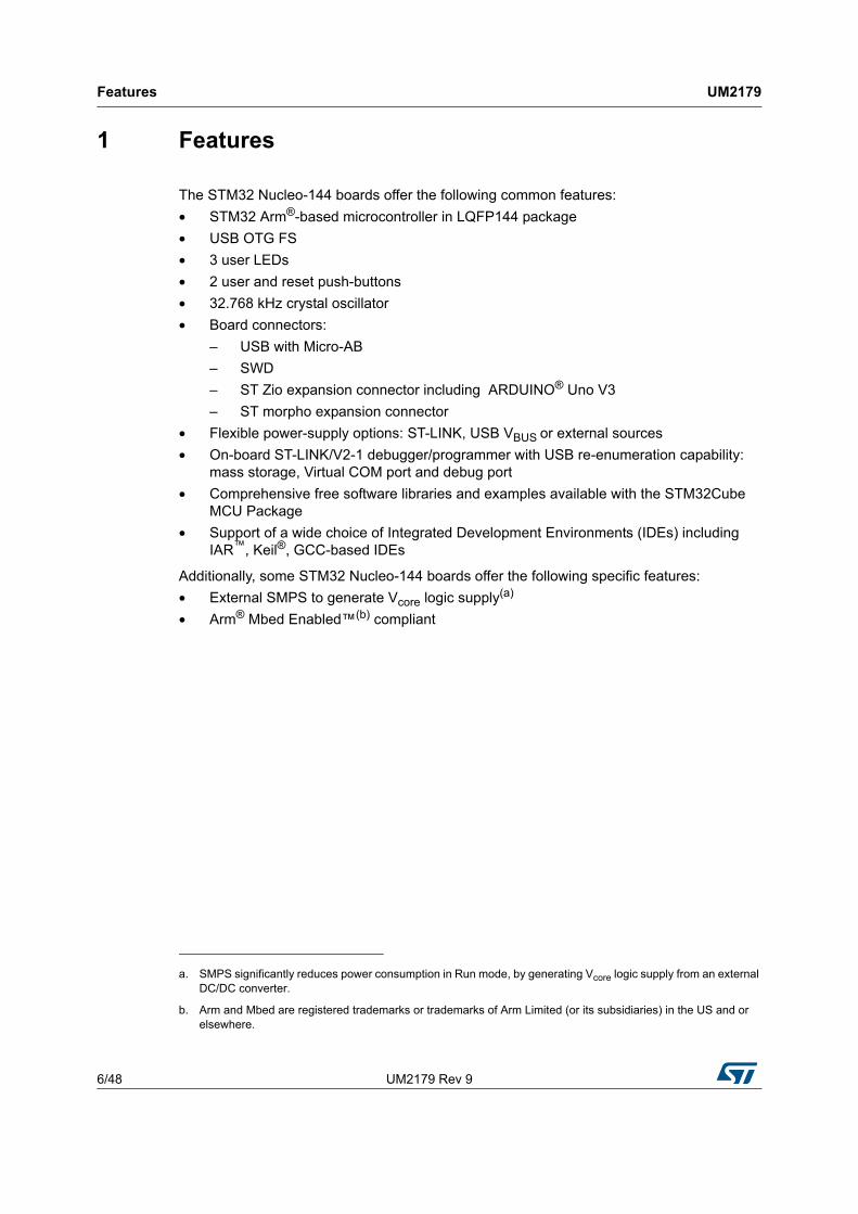
1 Features
The STM32 Nucleo-144 boards offer the following common features:
• STM32 Arm®-based microcontroller in LQFP144 package
• USB OTG FS
• 3 user LEDs
• 2 user and reset push-buttons
• 32.768 kHz crystal oscillator
• Board connectors:
– USB with Micro-AB
– SWD
– ST Zio expansion connector including ARDUINO® Uno V3
– ST morpho expansion connector
• Flexible power-supply options: ST-LINK, USB VBUS or external sources
• On-board ST-LINK/V2-1 debugger/programmer with USB re-enumeration capability: mass storage, Virtual COM port and debug port
• Comprehensive free software libraries and examples available with the STM32Cube MCU Package
• Support of a wide choice of Integrated Development Environments (IDEs) including IAR™, Keil®, GCC-based IDEs
Additionally, some STM32 Nucleo-144 boards offer the following specific features:
• External SMPS to generate Vcore logic supply(a)
• Arm® Mbed Enabled™(b) compliant
a. SMPS significantly reduces power consumption in Run mode, by generating Vcore logic supply from an external DC/DC converter.
b. Arm and Mbed are registered trademarks or trademarks of Arm Limited (or its subsidiaries) in the US and or elsewhere.

UM2179 Rev 9 7/48
UM2179 Ordering information
47
2 Ordering information
To order an STM32 Nucleo-144 board, refer to Table 1. Additional information is available from the datasheet and reference manual of the target STM32.
2.1 Product marking
Evaluation tools marked as “ES” or “E” are not yet qualified and therefore not ready to be used as reference design or in production. Any consequences deriving from such usage will not be at ST charge. In no event, ST will be liable for any customer usage of these engineering sample tools as reference design or in production.
“E” or “ES” marking examples of location:
• On the targeted STM32 that is soldered on the board (for illustration of STM32 marking, refer to the STM32 datasheet “Package information” paragraph at the www.st.com website).
• Next to the evaluation tool ordering part number that is stuck or silk-screen printed on the board.
The boards feature a specific STM32 device version, which allows the operation of any bundled commercial stack/library available. This STM32 device shows a "U" marking option at the end of the standard part number and is not available for sales.
In order to use the same commercial stack in his application, a developer may need to purchase a part number specific to this stack/library. The price of those part numbers includes the stack/library royalties.
Table 1. Ordering information
Order code Board reference Target STM32 Differentiating features
NUCLEO-L496ZG
MB1312
STM32L496ZGT6U Arm® Mbed Enabled™
NUCLEO-L496ZG-P STM32L496ZGT6PU External SMPS
NUCLEO-L4A6ZG STM32L4A6ZGT6U Cryptography
NUCLEO-L4P5ZG STM32L4P5ZGT6U -
NUCLEO-L4R5ZI STM32L4R5ZIT6U Arm® Mbed Enabled™
NUCLEO-L4R5ZI-P STM32L4R5ZIT6PU– Arm® Mbed Enabled™
– External SMPS

Ordering information UM2179
8/48 UM2179 Rev 9
2.2 Codification
The meaning of the codification is explained in Table 2.
The order code is mentioned on a sticker placed on the top side of the board.
Table 2. Codification explanation
NUCLEO-XXYYZT(-P) Description Example: NUCLEO-L496ZG-P
XX MCU series in STM32 Arm Cortex MCUs STM32L4 Series
YY MCU product line in the series STM32L496
Z STM32 package pin count 144 pins
T
STM32 Flash memory size:
– G for 1 Mbyte
– I for 2 Mbytes
1 Mbyte
-P STM32 has external SMPS function External SMPS

UM2179 Rev 9 9/48
UM2179 Quick start
47
3 Quick start
This section describes how to start a development quickly using the STM32 Nucleo-144 board.
Before installing and using the product, accept the Evaluation Product License Agreement from the www.st.com/epla webpage. For more information on the STM32 Nucleo-144 board and for demonstration software, visit the www.st.com/stm32nucleo webpage.
3.1 Getting started
Follow the sequence below to configure the Nucleo-144 board and launch the demonstration application (for components location refer to Figure 4: STM32 Nucleo-144 board top layout).
1. Check the jumper position on the board: JP1 (PWR-EXT) OFF (see Section 5.5.1: Power supply input from ST-LINK/V2-1 USB connector for more details) JP6 (Power source) on STLK side (for more details see Table 7: Power related jumper) JP5 (IDD) ON (for more details see Section 5.8: JP5 (IDD)) CN4 ON selected (for more details see Table 4: CN4 states of the jumpers).
2. For the correct identification of the device interfaces from the host PC and before connecting the board, install the Nucleo USB driver available on the www.st.com/stm32nucleo website.
3. To power the board connect the STM32 Nucleo-144 board to a PC with a USB ‘Type-A to Micro-B’ cable through the USB connector CN1 on the ST-LINK. As a result, the green LED LD6 (PWR) and LD4 (COM) light up and the red LED LD3 blinks.
4. Press button B1 (left button).
5. Observe that the blinking frequency of the three LEDs LD1 to LD3 changes, by clicking on the button B1.
6. The software demonstration and the several software examples, that allow the user to use the Nucleo features, are available at the www.st.com/stm32nucleo webpage.
7. Develop an application, using the available examples.
3.2 System requirements
• Windows® OS (7, 8 and 10), Linux® 64-bit or macOS®(a)
• USB Type-A to Micro-B cable
3.3 Development toolchains
• Keil® MDK-ARM(b)
• IAR™ EWARM(b)
• GCC-based IDEs
• Arm® Mbed™ online (see https://mbed.org)
a. macOS® is a trademark of Apple Inc., registered in the U.S. and other countries
b. On Windows® only.

Conventions UM2179
10/48 UM2179 Rev 9
3.4 Demonstration software
The demonstration software, included in the STM32Cube MCU Package corresponding to the on-board MCU, is preloaded in the STM32 Flash memory for easy demonstration of the device peripherals in standalone mode. The latest versions of the demonstration source code and associated documentation can be downloaded from the www.st.com/stm32nucleo webpage.
4 Conventions
Table 3 provides the conventions used for the ON and OFF settings in the present document.
In this document the references for all information that is common to all sale types, are “STM32 Nucleo-144 board” and “STM32 Nucleo-144 boards”.
Table 3. ON/OFF conventions
Convention Definition
Jumper JPx ON Jumper fitted
Jumper JPx OFF Jumper not fitted
Solder bridge SBx ON SBx connections closed by solder or 0 ohm resistor
Solder bridge SBx OFF SBx connections left open

UM2179 Rev 9 11/48
UM2179 Hardware layout and configuration
47
5 Hardware layout and configuration
The STM32 Nucleo-144 board is designed around the STM32 microcontrollers in a 144-pin LQFP package.
Figure 3 shows the connections between the STM32 microcontroller and its peripherals (ST-LINK/V2-1, push-buttons, LEDs, USB, ST Zio connectors and ST morpho headers).
Figure 4 and Figure 5 show the location of these features on the STM32 Nucleo-144 board. Figure 6 and Figure 7 show the mechanical dimensions of the STM32 Nucleo-144 board.
Figure 3. Hardware block diagram
1. Ext SMPS function is only available on '-P' suffixed boards.
Embedded ST-LINK/V2-1
STM32 Microcontroller
RESET
SWD
ST
orph
o ex
tens
ion
Head
er
ST
orph
o ex
tens
ion
Head
er
Micro-BUSB
onnector
IO
USBB2RST
B1USER
IOZi
o on
nect
orLEDLD1
ST-LINK Part
MCU Part
LEDLD2/3
Micro-AB or Micro-B USB
onnector
Zio
onne
ctor
Ext SMPS
IO

Hardware layout and configuration UM2179
12/48 UM2179 Rev 9
5.1 STM32 Nucleo-144 board layout
Figure 4. STM32 Nucleo-144 board top layout
CN1 ST-LINK Micro USB connector
CN4 ST-LINK/ NUCLEO selector
LD1-LD3User LEDs
B1User button
CN11 ST orphopin header
CN13SMPS signal connector
JP1 PWR-EXT
CN5 SWD connector
JP5 IDD measurement
U11 STM32 Microcontroller
LD7USB over
CN7, CN10Zio connectors
SB63.3V regulator output
JP6Power Source selection
LD6Power (Green LED)
LD5(Red LED) ST-Power Over
LD4(Red/Green LED) COM
LD8 USB VBUS
CN14User USB connector
B2Reset button
CN8, CN9Zio connectors CN12
ST orphopin header

UM2179 Rev 9 13/48
UM2179 Hardware layout and configuration
47
Figure 5. STM32 Nucleo-144 board bottom layout
SB101, SB103, SB105, SB107 (RESERVED)
SB100, SB102, SB104, SB106 (DEFAULT)

Hardware layout and configuration UM2179
14/48 UM2179 Rev 9
5.2 STM32 Nucleo-144 board mechanical drawing
Figure 6. STM32 Nucleo-144 board mechanical drawing in millimeter

UM2179 Rev 9 15/48
UM2179 Hardware layout and configuration
47
Figure 7. Nucleo-144 board mechanical drawing in mils
Hardware layout and configuration UM2179
16/48 UM2179 Rev 9
5.3 Cuttable PCB
The STM32 Nucleo-144 board is divided into two parts: ST-LINK and target STM32. The ST-LINK part of the PCB can be cut out to reduce the board size. In this case the remaining target STM32 part can only be powered by VIN, E5V and 3.3 V on the ST morpho connector CN11, or by VIN and 3.3 V on the ST Zio connector CN8. It is still possible to use the ST-LINK part to program the STM32, using wires between the CN5 and SWD available signals on the ST morpho connector (SWCLK CN11 pin 15, SWDIO CN11 pin 13 and NRST CN11 pin 14, same I/O level as VDD_MCU).
5.4 Embedded ST-LINK/V2-1
The ST-LINK/V2-1 programming and debugging tool is integrated in the STM32 Nucleo-144 board.
The embedded ST-LINK/V2-1 supports only SWD for STM32 devices. For information about debugging and programming features refer to the ST-LINK/V2 in-circuit debugger/programmer for STM8 and STM32 user manual (UM1075), which describes in details all the ST-LINK/V2 features.
The changes versus ST-LINK/V2 version are listed below. New features supported on ST-LINK/V2-1:
• USB software re-enumeration
• Virtual COM port interface on USB
• Mass storage interface on USB
• USB power management request for more than 100 mA power on USB
Features not supported on ST-LINK/V2-1:
• SWIM interface
• Minimum supported application voltage limited to 3 V
There are two different ways to use the embedded ST-LINK/V2-1, depending on the jumper state (see Table 4):
• Program/debug the STM32 on board
• Program/debug the STM32 in an external application board, using a cable connected to SWD connector CN5
Table 4. CN4 states of the jumpers
Jumper state Description
Both CN4 jumpers ONST-LINK/V2-1 functions enabled for on-board programming (default). See Section 5.4.3.
Both CN4 jumpers OFFST-LINK/V2-1 functions enabled for external CN5 connector (SWD supported). See Section 5.4.4.

UM2179 Rev 9 17/48
UM2179 Hardware layout and configuration
47
5.4.1 Drivers
Before connecting the Nucleo-144 board to a Windows® (XP, 7, 8 and 10) PC via USB, install the driver for ST-LINK/V2-1 that can be downloaded from the www.st.com website.
If the STM32 Nucleo-144 board is connected to the PC before installing the driver, the PC device manager may report some Nucleo interfaces as “Unknown”.
To recover from this situation, after installing the dedicated driver, the association of “Unknown” USB devices found on the STM32 Nucleo-144 board to this dedicated driver, must be updated in the device manager manually.
Note: It is recommended to proceed by using USB Composite Device, as shown in Figure 8.
Figure 8. USB composite device
5.4.2 ST-LINK/V2-1 firmware upgrade
The ST-LINK/V2-1 embeds a firmware upgrade mechanism for in-situ upgrade through the USB port. As the firmware may evolve during the lifetime of the ST-LINK/V2-1 product (for example new functionalities, bug fixes, support for new microcontroller families), it is recommended to keep the ST-LINK/V2-1 firmware up to date before starting to use the STM32 Nucleo-144 board. The latest version of this firmware is available from the www.st.com website.
5.4.3 Using the ST-LINK/V2-1 to program and debug the on-board STM32
To program the on-board STM32, place the two jumpers marked in red on the connector CN4, as shown in Figure 9. The CN5 connector must not be used, since it could disturb the communication with the STM32 microcontroller of the Nucleo-144 board.

Hardware layout and configuration UM2179
18/48 UM2179 Rev 9
Figure 9. Connecting the STM32 Nucleo-144 board to program the on-board STM32
5.4.4 Using ST-LINK/V2-1 to program and debug an external STM32 application
It is very easy to use the ST-LINK/V2-1 to program the STM32 on an external application.
Simply remove the two jumpers from CN4, as shown in Figure 10 and connect the application to the SWD debug connector according to Table 5.
Note: JP4 NRST (target STM32 RESET) must be open when CN3 pin 5 is used in an external application.

UM2179 Rev 9 19/48
UM2179 Hardware layout and configuration
47
Table 5. Debug connector CN5 (SWD)
Pin CN5 Description
1 VDD_TARGET VDD from application
2 SWCLK SWD clock
3 GND ground
4 SWDIO SWD data input/output
5 NRST RESET of target STM32
6 SWO Reserved

Hardware layout and configuration UM2179
20/48 UM2179 Rev 9
Figure 10. Using ST-LINK/V2-1 to program an external STM32 application

UM2179 Rev 9 21/48
UM2179 Hardware layout and configuration
47
5.5 Power supply and power selection
The power supply is provided either by the host PC through the USB cable or by an external source: VIN (7 V-12 V), E5V (5 V) or +3.3 V power supply pins on CN8 or CN11. If VIN, E5V or +3.3 V is used to power a Nucleo-144 board, this power source must comply with the standard EN-60950-1: 2006+A11/2009 and must be Safety Extra Low Voltage (SELV) with limited power capability.
If the power supply is +3.3 V, the ST-LINK is not powered and cannot be used.
5.5.1 Power supply input from ST-LINK/V2-1 USB connector
The STM32 Nucleo-144 board and shield can be powered from the ST-LINK USB connector CN1 (U5V), by placing a jumper between the pins 3 and 4 of JP6, as shown in Table 7: Power related jumper. Note that only the ST-LINK part is power supplied before the USB enumeration, as the host PC only provides 100 mA to the board at that time. During the USB enumeration, the STM32 Nucleo-144 board requires 300 mA of current to the host PC. If the host is able to provide the required power, the targeted STM32 microcontroller is powered and the green LED LD6 is turned ON, thus the STM32 Nucleo-144 board and its shield can consume a maximum current of 300 mA, not more. If the host is not able to provide the required current, the targeted STM32 microcontroller and the extension boards are not power supplied. As a consequence the green LED LD6 stays turned OFF. In such case it is mandatory to use an external power supply as explained in the next section.
After the USB enumeration succeeds, the ST-LINK U5V power is enabled, by asserting the PWR_EN pin. This pin is connected to a power switch (ST890), which powers the board.
This power switch also features a current limitation to protect the PC if a short-circuit happens on the board. If an overcurrent (more than 500 mA) happens on the board, the red LED LD5 lits up.
Warning: If the maximum current consumption of the STM32 Nucleo-144 board and its shield boards exceed 300 mA, it is mandatory to power the STM32 Nucleo-144 board, using an external power supply connected to E5V, VIN or +3.3 V.
Note: If the board is powered by a USB charger, there is no USB enumeration, so the green LED LD6 stays in OFF state permanently and the target STM32 is not powered. In this specific case a jumper must be placed between pins 5 and 6 of JP6, to allow the board to be powered anyway.
5.5.2 External power supply inputs
Depending on the used voltage, an external power source supplies in three different ways the STM32 Nucleo-144 board and its shield boards. The three power sources are listed in Table 6.
When the STM32 Nucleo-144 board is power supplied by VIN or E5V, the jumper configuration must be as showed below:
• Jumper JP6 on pin 1 and pin 2 for E5V or jumper JP6 on pin 7 and pin 8 for VIN
• Jumper JP1 OFF

Hardware layout and configuration UM2179
22/48 UM2179 Rev 9
The 5 V power source is selected by the jumper JP6 as shown in Table 7.
Table 6. External power sources
Input power name
Connector pins
Voltage range
Max current Limitation
VINCN8 pin 15 CN11 pin 24
7 V to 12 V 800 mA
From 7 V to 12 V only and input current capability is linked to input voltage:
– 800 mA input current when VIN=7 V
– 450 mA input current when 7V<VIN<9V
– 250 mA input current when 9 V<VIN<12 V
E5V CN11 pin 64.75 V to 5.25 V
500 mA -
+3.3 VCN8 pin 7
CN11 pin 163 V to 3.6 V -
Two possibilities:
– ST-LINK PCB is cut
– SB3 and SB111 OFF (ST-LINK not powered)
Table 7. Power related jumper
Jumper Description
JP6
STLK (ST-LINK VBUS) is used as power source when JP6 is set as shown on the right (Default setting)
E5V is used as power source when JP6 is set as shown on the right:
CHGR (USB Charger on CN1) is used as power source when JP6 is set as shown on the right:
VIN is used as power source when JP6 is set as shown on the right:
E5V STLK CHGR VIN
E5V STLK CHGR VIN
E5V STLK CHGR VIN
E5V STLK CHGR VIN

UM2179 Rev 9 23/48
UM2179 Hardware layout and configuration
47
Using VIN or E5V as an external power supply
When powered by VIN or E5V, it is still possible to use the ST-LINK for only programming or debugging, but it is mandatory to power the board first using VIN or E5V, then to connect the USB cable to the PC. In this way the enumeration succeeds, thanks to the external power source.
The following power-sequence procedure must be respected:
1. Connect jumper JP6 between pin 1 and pin 2 for E5V or between pin 7 and pin 8 for VIN
2. Check that JP1 is removed
3. Connect the external power source to VIN or E5V
4. Power on the external power supply 7 V< VIN < 12 V to VIN, or 5 V for E5V
5. Check that the green LED LD6 is turned ON
6. Connect the PC to the USB connector CN1
If this order is not respected, the board may be powered by USB (U5V) first, then by VIN or E5V as the following risks may be encountered:
1. If the board needs more than 300 mA, the PC may be damaged or the current supplied can be limited by the PC. As a consequence the board is not powered correctly.
2. 300 mA is requested during the enumeration phase (since JP1 must be OFF) so there is the risk that the request is rejected and the enumeration does not succeed if the PC cannot provide such current. Consequently the board is not power supplied (LED LD6 remains OFF).
External power supply input: + 3.3 V
If 3.3 V is provided by a shield board, it is worth using the +3.3 V (CN8 pin 7 or CN11 pin 16) directly as power input. In this case the ST-LINK is not powered thus the programming and debugging features are not available.
When the board is powered with +3.3 V, two different configurations are possible:
• ST-LINK is removed (PCB cut)
• SB6 (3.3 V regulator) and JP3 (NRST) are OFF
5.5.3 External power supply output
When powered by USB, VIN or E5V, the +5 V (CN8 pin 9 or CN11 pin 18) can be used as output power supply for an ST Zio shield or an extension board. In this case the maximum current of the power source specified in Table 6: External power sources must be respected.
The +3.3 V (CN8 pin 7 or CN11 pin 16) can also be used as power supply output. The current is limited by the maximum current capability of the regulator U6 (500 mA max).
5.5.4 SMPS power supply
Power figures in Run Mode are significantly improved, by generating Vcore logic supply from the external DC/DC converter (this function is only available on '-P' suffixed boards).
Board is populated with two different SMPS mounted on U15 and U16:
• SMPS U15 allows to dynamically supply the VDD_1V2 pins in Run mode at 1.1 V with a maximum current of 30 mA. For the NUCLEO-L4R5ZI-P, the VDD_1V2 pins in Run mode are supplied at 1.2 V with a maximum current of 40 mA.

Hardware layout and configuration UM2179
24/48 UM2179 Rev 9
• SMPS U16 allows to supply the VDD_MCU pins at 1.8 V with a maximum current of 50 mA. When SB125 is opened and SB120 closed, the SMPS can deliver higher current but with higher consumption. This SMPS is disabled by default (See Table 10: Configuration of the solder bridges and jumpers).
VDD_MCU solder bridge configuration:
• 3.3 V (default): SB122 closed, SB121 and SB127 open
• 1.8 V: SB122 open, and SB121 and SB127 closed (best ULPBench score)
Caution: The power sequence is not respected when using 1V8 MCU_VDD. Refer to the Getting started with STM32L4 Series and STM32L4+ Series hardware development application note (AN4555), and to the corresponding STM32L4 Series and STM32L4+ Series product datasheets.
Note: The ST-LINK is still available in this configuration as a result of level shifter U14.
5.6 LEDs
User LD1: a green user LED is connected to the STM32 I/O PC7 (SB124 ON and SB123 OFF) or PA5 (SB123 ON and SB124 OFF) corresponding to the ST Zio D13. It only works when VCC_MCU is 3.3 V.
User LD2: a blue user LED is connected to PB7.
User LD3: a red user LED is connected to PB14.
These user LEDs are on when the I/O is HIGH value, and are off when the I/O is LOW.
LD4 COM: the tricolor LED LD4 (green, orange and red) provides information about ST-LINK communication status. LD4 default color is red. LD4 turns to green to indicate that the communication is in progress between the PC and the ST-LINK/V2-1, with the following setup:
• Slow blinking red/off: at power-on before USB initialization
• Fast blinking red/off: after the first correct communication between PC and ST-LINK/V2-1 (enumeration)
• Red LED on: when the initialization between the PC and ST-LINK/V2-1 is complete
• Green LED on: after a successful target communication initialization
• Blinking red/green: during communication with target
• Green on: communication finished and successful
• Orange on: communication failure
LD5 USB power fault: LD5 indicates that the board power consumption on USB exceeds 500 mA, consequently the user must power the board using an external power supply.
LD6 PWR: the green LED indicates that the STM32 part is powered and +5 V power is available on CN8 pin 9 and CN11 pin 18.
LD7 and LD8 USB FS: refer to Section 5.12: USB FS OTG.
Note:1 LD1 is connected to U8 and it is driven by PC7 or PA5 which may be changed to 1.8 V I/O, so LD1 cannot be lit when VDD is set to 1.8 V.
Note:2 LD2, LD3 cannot work with VDD_MCU= 1.8 V

UM2179 Rev 9 25/48
UM2179 Hardware layout and configuration
47
5.7 Push-buttons
B1 USER: the user button is connected to the I/O PC13 by default (Tamper support, SB197 ON and SB178 OFF) or PA0 (Wakeup support, SB178 ON and SB197 OFF) of the STM32.
B2 RESET: this push-button is connected to NRST and is used to RESET the STM32.
5.8 JP5 (IDD)
The jumper JP5, labeled IDD, is used to measure the STM32 microcontroller consumption by removing the jumper and by connecting an ammeter:
• JP5 ON: STM32 is powered (default)
• JP5 OFF: an ammeter must be connected to measure the STM32 current. If there is no ammeter, the STM32 is not powered
5.9 OSC clock
5.9.1 OSC clock supply
There are four ways to configure the pins corresponding to the external high-speed clock (HSE):
• HSE not used (Default): PF0/PH1 and PF1/PH1 are used as GPIOs instead of as clock. The configuration must be:
– SB147 and SB156 ON
– SB109 and SB148 (MCO) OFF
– SB12 and SB13 removed
• MCO from ST-LINK: MCO output of ST-LINK is used as input clock. This frequency cannot be changed, it is fixed at 8 MHz and connected to the
• PF0/PH0-OSC_IN of STM32 microcontroller. The configuration must be:
– SB147 OFF
– SB109 and SB148 ON
– SB12 and SB13 OFF
• HSE on-board oscillator from X3 crystal (not provided): for typical frequencies and its capacitors and resistors, refer to the STM32 microcontroller datasheet and for the oscillator design guide refer to the Oscillator design guide for STM8S, STM8A and STM32 microcontrollers Application note (AN2867). The X3 crystal has the following characteristics: 8 MHz, 8 pF, 20 ppm. It is recommended to use the NX3225GD-8.000M- EXS00A-CG04874 crystal manufactured by NIHON DEMPA KOGYO CO., LTD. The configuration must be:
– SB147 and SB156 OFF
– SB12 and SB13 soldered
– C37 and C38 soldered with 4.3 pF capacitors
– SB109 and SB148 OFF

Hardware layout and configuration UM2179
26/48 UM2179 Rev 9
• Oscillator from external PF0/PH0: from an external oscillator through the pin 29 of the CN11 connector. The configuration must be:
– SB147 ON
– SB109 and SB148 OFF
– SB12 and SB13 removed
5.10 OSC 32 KHz clock supply
There are three ways to configure the pins corresponding to low-speed clock (LSE):
• On-board oscillator (Default): X2 crystal. Refer to the Oscillator design guide for STM8S, STM8A and STM32 microcontrollers Application note (AN2867) for oscillator design guide for STM32 microcontrollers. It is recommended to use the NX3214SA- 32.768KHZ-EXS00A-MU00525 (32.768 KHz, 6 pF load capacitance, 200 ppm) crystal from Nihon Dempa Kogyo CO, LTD.
• Oscillator from external PC14: from external oscillator through the pin 25 of CN11 connector. The configuration must be:
– SB145 and SB146 ON
– R39 and R40 removed
• LSE not used: PC14 and PC15 are used as GPIOs instead of low-speed clock. The configuration must be:
– SB145 and SB146 ON
– R39 and R40 removed
5.11 LPUART1 communication
The LPUART1 interface available on PG7 and PG8 of the STM32 can be connected to the ST-LINK or to the ST morpho connector. Another option to do this connection is to set the related solder bridges. By default the LPUART1 communication between the target STM32 and the ST-LINK is enabled, to support the Virtual COM port (SB130 and SB131 ON). Refer to Table 8.
Table 8. LPUART1 pin configuration
Pin name
FunctionVirtual COM port (default
configuration)ST morpho connection
PG7 LPUART1 TX SB131 ON and SB195 OFF SB131 OFF and SB195 ON
PG8 LPUART1 RX SB130 ON and SB193 OFF SB130 OFF and SB193 ON

UM2179 Rev 9 27/48
UM2179 Hardware layout and configuration
47
5.12 USB FS OTG
The STM32 Nucleo-144 board supports the USB OTG as host or as device-full-speed communication through a USB Micro-AB connector (CN14) and USB power switch (U12) connected to VBUS.
Warning: The USB Micro-AB connector (CN14) cannot power a Nucleo-144 board. To avoid damaging the STM32, it is mandatory to power the board before connecting a USB cable on CN14. Otherwise there is a risk of current injection on STM32 I/Os.
A green LED LD8 lits up in one of these cases:
• Power switch (U12) is ON and STM32 Nucleo-144 board works as a USB host
• VBUS is powered by another USB host when the STM32 Nucleo-144 board works as a USB device.
The red LED LD7 lits up if overcurrent occurs when +5 V is enabled on VBUS in USB host mode.
Note:1 It is recommended to power the Nucleo-144 board with an external power supply when using the USB OTG or the host function.
Note:2 JP4 must be closed when using the USB OTG FS.
Note:3 Limitation: when the cable is not connected, PA9 (VBUS) is not floating, because internal pull up of PA12 (D+) impacts PA9 through ESD protection part USBLC6-2SC6 (U13).
For pin configuration refer to Table 9.
Table 9. USB pin configuration
Pin name
FunctionConfiguration
when using USB connector
Configuration when using ST
morpho connectorRemark
PA8 USB SOF - - Test point TP1
PA9 USB VBUS SB135 ON SB135 OFF -
PA10 USB ID SB134 ON SB134 OFF -
PA11 USB DM SB142 ON SB142 OFF -
PA12 USB DP SB143 ON SB143 OFF -
PG6 USB GPIO OUTOTG:SB201 OFF,
SB200 ONOTG:SB200 OFF
OTG:USB power switch control
PG5 USB GPIO INJP4 ON, SB199 OFF SB198 ON
JP4 OFF USB overcurrent alarm

Hardware layout and configuration UM2179
28/48 UM2179 Rev 9
5.13 Solder bridges and jumpers
SBxx are located on top layer and SB1xx-SB2xx on bottom layer of the STM32 Nucleo-144 board. The configuration of the solder bridges and jumpers is showed in Table 10.
Table 10. Configuration of the solder bridges and jumpers
Bridge/jumper State(1) Description
SB5 (+3V3_PER)ON Peripheral power +3V3_PER is connected to +3.3 V.
OFF Peripheral power +3V3_PER is not connected.
SB6 (3.3 V)ON
Output of voltage regulator LD39050PU33R is connected to 3.3 V.
OFF Output of voltage regulator LD39050PU33R is not connected.
SB195, SB193 (GPIO)
ONPG7 and PG8 on STM32 are connected to ST morpho connectors CN12. If these pins are used on ST morpho connectors, SB130 and SB131 should be OFF.
OFFPG7 and PG8 on STM32 are disconnected to ST morpho connectors CN12.
SB131, SB130 (ST-LINK-USART)
ONPA2 and PA3 on ST-LINK STM32F103CBT6 are connected to PG7 and PG8 to enable the Virtual COM port. Thus PG7 and PG8 on ST morpho connectors cannot be used.
OFFPA2 and PA3 on ST-LINK STM32F103CBT6 are disconnected to PG7 and PG8 on STM32.
SB152 (VDDA)ON VDDA on STM32 MCU is connected to VDD.
OFF VDDA on STM32 MCU is disconnected to VDD.
SB100,102,104,106 (DEFAULT)
ON Reserved, do not modify.
SB101,103,105,107 (RESERVED)
OFF Reserved, do not modify.
SB141 (SWO)ON
SWO signal of the STM32 (PB3) is connected to ST-LINK SWO input.
OFF SWO signal of STM32 is not connected.
SB110, SB111,SB112 (IOREF)
OFF, OFF, ON
IOREF is connected to VDD_MCU.
ON, OFF, OFF
IOREF is connected to +3.3 V.
OFF, ON, OFF
IOREF is connected to +3V3_PER.
SB119 (VREF+)
OFFPin 6 of CN7 and Pin 7 of CN12 are disconnected to VREF+ on STM32.
ONPin 6 of CN7 and Pin 7 of CN12 are connected to VREF+ on STM32.
SB137 (SDMMC_D0), SB136 (SDMMC_D1)
ON These pins are connected to ST morpho connector CN12.
OFFThese pins are disconnected from ST morpho connector CN12 to avoid stub of SDMMC data signals on PCB.

UM2179 Rev 9 29/48
UM2179 Hardware layout and configuration
47
SB124, SB123(LD1-LED)
ON, OFF Green user LED LD1 is connected to PC7.
OFF,ONGreen user LED LD1 is connected to D13 of ARDUINO® signal (PA5).
OFF, OFF Green user LED LD1 is not connected.
ON,ON Forbidden.
SB172 (Legacy)
SB173 (SMPS) (LD2-LED)
ON Blue user LED LD2 is connected to PB7.
OFF Blue user LED LD2 is not connected.
SB132 (LD3-LED)ON Red user LED LD3 is connected to PB14.
OFF Red user LED LD3 is not connected.
SB145,146
(X2 crystal)
OFFPC14, PC15 are not connected to ST morpho connector CN11. (X2 used to generate 32 kHz clock).
ONPC14, PC15 are connected to ST morpho connector CN11. (R39 and R40 must be removed).
SB147 (PH0), SB156
(PH1) (Main clock)
ON, ONPH0 and PH1 are connected to ST morpho connector CN11. (SB12, SB13 and SB148 must be removed).
OFF, ONPH0 is not connected to ST morpho
PH1 is connected to ST morpho connector CN11 (MCO is used as main clock for STM32 on PH0).
OFF, OFFPH0, PH1 are not connected to ST morpho connector CN11 (X3, C37, C38, SB12 and SB13 provide a clock. In this case SB148 must be removed).
SB109, SB148 (MCO)
OFFMCO of ST-LINK (STM32F103CBT6) is not connected to PH0 of STM32.
ONMCO of ST-LINK (STM32F103CBT6) is connected to PH0 of STM32.
SB12, SB13 (external 8M crystal)
OFF PH0 and PH1 are not connected to external 8 MHz crystal X3.
ON PH0 and PH1 are connected to external 8 MHz crystal X3.
SB154 (VBAT)ON VBAT pin of STM32 is connected to VDD.
OFF VBAT pin of STM32 is not connected to VDD.
SB197, SB178(B1-USER)
ON, OFF B1 push-button is connected to PC13.
OFF, ONB1 push-button is connected to PA0 (Set SB179 OFF if ST Zio connector is used).
OFF, OFF
B1 push-button is not connected.
SB179 (PA0)ON PA0 is connected to ST Zio connector (Pin 29 of CN10).
OFF PA0 is not connected to ST Zio connector (Pin 29 of CN10).
SB151,SB153 OFF Default setting.
ON Forbidden.
Table 10. Configuration of the solder bridges and jumpers (continued)
Bridge/jumper State(1) Description

Hardware layout and configuration UM2179
30/48 UM2179 Rev 9
All the other solder bridges present on the STM32 Nucleo-144 board are used to configure several I/Os and power supply pins for compatibility of features and pinout with the target STM32 supported.
STM32 Nucleo-144 boards are delivered with the solder bridges configured according to the target STM32 supported.
SB158, SB167 (AVDD)ON, OFF AVDD on STM32 is connected to VDD.
OFF, ON AVDD on STM32 is connected to VDD_MCU.
SB142 (PA11), SB143 (PA12)
ON These pins are used as D+ and D- on USB connector CN14.
OFF These pins are used as GPIOs on ST morpho connectors.
SB149 (VREF+)ON VREF+ on STM32 is connected to AVDD.
OFF VREF+ on STM32 is disconnected to AVDD.
SB144 (QSPI_IO1)
ON These pins are connected to ST morpho connector CN11.
OFFThese pins are disconnected from ST morpho connector CN11 to avoid stub of QSPI_IO1 signals on PCB.
JP2(2) (STM_RST)
OFF No incidence on ST-LINK STM32F103CBT6 NRST signal.
ONST-LINK STM32F103CBT6 NRST signal is connected to GND (ST-LINK reset to reduce power consumption).
JP3 (NRST)
ONBoard RESET signal (NRST) is connected to ST-LINK reset control I/O (T_NRST).
OFFBoard RESET signal (NRST) is not connected to ST-LINK reset control I/O (T_NRST).
SB122, SB121, SB127 (VDD_MCU)
ON, OFF,OFF
VDD_MCU is connected to VDD directly (3.3 V fixed).
OFF, ON, ON
VDD_MCU is connected to output of DC-DC (1.8 V fixed).
1. Default SBx state is shown in bold.
2. The jumper JP2 is not mounted on the board by default.
Table 10. Configuration of the solder bridges and jumpers (continued)
Bridge/jumper State(1) Description

UM2179 Rev 9 31/48
UM2179 Hardware layout and configuration
47
5.14 Expansion connectors
For each STM32 Nucleo-144 board, Figure 11, Figure 12, Figure 13, Figure 14, Figure 15 and Figure 16 show the signals connected by default to the ST Zio connectors (CN7, CN8, CN9 and CN10), including the support for ARDUINO® Uno V3.
Figure 11. NUCLEO-L496ZG
NUCLEO-L496ZG
CN7
CN10
CN8
CN9
135791113151719
2468101214161820
13579111315
246810121416
1357911131517192123252729
24681012141618202224262830
13579111315171921232527293133
246810121416182022242628303234
PC8
PF5PF3PD2PC12PC11PC10PC9
GNDPD3PD4PD5PD6PD7
PG1PF9PF7PF8PE3PE6
PE4PE2
PE5
D34D33D32
GNDD31D30D29D28
GND
D25D24D23D22D21D20D19D18D17D16
D27D26
A8A7A6
GNDAGNDAVDD
PE0PB0PA0
GNDPE14PE12
PB0PE15GND
PB4PA4PB3PB5PB4PA4
PB12PB13PB15PC6
PB10PA2PA1PC2PB1
GNDAGNDAVDDD50
D49D48D47D46D45D44D43
GNDD55D54D53D52D51
D64D63D62D61D60D59D58D57D56
Arduino subset of Zio = A0 to A5 and D0 to D15
Zio extension = A6 to A8 and D16 to D72
USB OTG
USBST-LINK
D65D66D67
GNDD68D69D70D71D72
VINGNDGND+5V
+3V3RESETIOREF
NC
A5A4A3A2A1A0
PG0PD1PD0GNDPF0PF1PF2PB6PB2
VINGNDGND+5V
+3V3RESETIOREF
NC
PC5PC4PC1PC3PC0PA3
PF12PD15PD14PA7PA6PA5GNDNCPB9PB8
PD9PD8PF15PE13PF14PE11PE9PF13
PB11PB10PE15PE14PE12PE10
PE7PE8
GND
D8D9D10D11D12D13GNDAVDDD14D15
D0D1D2D3D4D5D6D7
D35D36D37D38D39D40GNDD41D42

Hardware layout and configuration UM2179
32/48 UM2179 Rev 9
Figure 12. NUCLEO-L496ZG-P
NUCLEO-L496ZG-P
CN7
CN10
CN8
CN9
135791113151719
2468101214161820
13579111315
246810121416
1357911131517192123252729
24681012141618202224262830
13579111315171921232527293133
246810121416182022242628303234
PC8
PF5PF3PD2PC12PC11PC10PC9
GNDPD3PD4PD5PD6PD7
PG1PF9PF7PF8PE3PE6
PE4PE2
PE5
D34D33D32
GNDD31D30D29D28
GND
D25D24D23D22D21D20D19D18D17D16
D27D26
A8A7A6
GNDAGNDAVDD
PE0PB0PA0
GNDPE14PE12
PB0PE15GND
PB4PA4PB3PB5PB4PA4
PB12PB13PB15PC6
PB10PA2PA1PC2PB1
GNDAGNDAVDDD50
D49D48D47D46D45D44D43
GNDD55D54D53D52D51
D64D63D62D61D60D59D58D57D56
Arduino subset of Zio = A0 to A5 and D0 to D15
Zio extension = A6 to A8 and D16 to D72
USB OTG
USBST-LINK
D65D66D67
GNDD68D69D70D71D72
VINGNDGND+5V
+3V3RESETIOREF
NC
A5A4A3A2A1A0
PG0PD1PD0GNDPF0PF1PF2PB6PB2
VINGNDGND+5V
+3V3RESETIOREF
NC
PC5PC4PC1PC3PC0PA3
PF12PD15PD14PA7PA6PA5GNDNCPB9PB8
PD9PD8PF15PE13PF14PE11PE9PF13
NCPB10PE15PE14PE12PE10
PE7PE8
GND
D8D9D10D11D12D13GNDAVDDD14D15
D0D1D2D3D4D5D6D7
D35D36D37D38D39D40GNDD41D42

UM2179 Rev 9 33/48
UM2179 Hardware layout and configuration
47
Figure 13. NUCLEO-L4A6ZG
NUCLEO-L4A6ZG
CN7
CN10
CN8
CN9
135791113151719
2468101214161820
13579111315
246810121416
1357911131517192123252729
24681012141618202224262830
13579111315171921232527293133
246810121416182022242628303234
PC8
PF5PF3PD2PC12PC11PC10PC9
GNDPD3PD4PD5PD6PD7
PG1PF9PF7PF8PE3PE6
PE4PE2
PE5
D34D33D32
GNDD31D30D29D28
GND
D25D24D23D22D21D20D19D18D17D16
D27D26
A8A7A6
GNDAGNDAVDD
PE0PB0PA0
GNDPE14PE12
PB0PE15GND
PB4PA4PB3PB5PB4PA4
PB12PB13PB15PC6
PB10PA2PA1PC2PB1
GNDAGNDAVDDD50
D49D48D47D46D45D44D43
GNDD55D54D53D52D51
D64D63D62D61D60D59D58D57D56
Arduino subset of Zio = A0 to A5 and D0 to D15
Zio extension = A6 to A8 and D16 to D72
USB OTG
USBST-LINK
D65D66D67
GNDD68D69D70D71D72
VINGNDGND+5V
+3V3RESETIOREF
NC
A5A4A3A2A1A0
PG0PD1PD0GNDPF0PF1PF2PB6PB2
VINGNDGND+5V
+3V3RESETIOREF
NC
PC5PC4PC1PC3PC0PA3
PF12PD15PD14PA7PA6PA5GNDNCPB9PB8
PD9PD8PF15PE13PF14PE11PE9PF13
PB11PB10PE15PE14PE12PE10
PE7PE8
GND
D8D9D10D11D12D13GNDAVDDD14D15
D0D1D2D3D4D5D6D7
D35D36D37D38D39D40GNDD41D42

Hardware layout and configuration UM2179
34/48 UM2179 Rev 9
Figure 14. NUCLEO-L4P5ZG

UM2179 Rev 9 35/48
UM2179 Hardware layout and configuration
47
Figure 15. NUCLEO-L4R5ZI
NUCLEO-L4R5ZI
CN7
CN10
CN8
CN9
135791113151719
2468101214161820
13579111315
246810121416
1357911131517192123252729
24681012141618202224262830
13579111315171921232527293133
246810121416182022242628303234
PC8
PF5PF3PD2PC12PC11PC10PC9
GNDPD3PD4PD5PD6PD7
PG1PF9PF7PF8PE3PE6
PE4PE2
PE5
D34D33D32
GNDD31D30D29D28
GND
D25D24D23D22D21D20D19D18D17D16
D27D26
A8A7A6
GNDAGNDAVDD
PE0PB0PA0
GNDPE14PE12
PB0PE15GND
PB4PA4PB3PB5PB4PA4
PB12PB13PB15PC6
PB10PA2PA1PC2PB1
GNDAGNDAVDDD50
D49D48D47D46D45D44D43
GNDD55D54D53D52D51
D64D63D62D61D60D59D58D57D56
Arduino subset of Zio = A0 to A5 and D0 to D15
Zio extension = A6 to A8 and D16 to D72
USB OTG
USBST-LINK
D65D66D67
GNDD68D69D70D71D72
VINGNDGND+5V
+3V3RESETIOREF
NC
A5A4A3A2A1A0
PG0PD1PD0GNDPF0PF1PF2PB6PB2
VINGNDGND+5V
+3V3RESETIOREF
NC
PC5PC4PC1PC3PC0PA3
PF12PD15PD14PA7PA6PA5GNDNCPB9PB8
PD9PD8PF15PE13PF14PE11PE9PF13
PB11PB10PE15PE14PE12PE10
PE7PE8
GND
D8D9D10D11D12D13GNDAVDDD14D15
D0D1D2D3D4D5D6D7
D35D36D37D38D39D40GNDD41D42

Hardware layout and configuration UM2179
36/48 UM2179 Rev 9
Figure 16. NUCLEO-L4R5ZI-P
NUCLEO-L4R5ZI-P
CN7
CN10
CN8
CN9
135791113151719
2468101214161820
13579111315
246810121416
1357911131517192123252729
24681012141618202224262830
13579111315171921232527293133
246810121416182022242628303234
PC8
PF5PF3PD2PC12PC11PC10PC9
GNDPD3PD4PD5PD6PD7
PG1PF9PF7PF8PE3PE6
PE4PE2
PE5
D34D33D32
GNDD31D30D29D28
GND
D25D24D23D22D21D20D19D18D17D16
D27D26
A8A7A6
GNDAGNDAVDD
PE0PB0PA0
GNDPE14PE12
PB0PE15GND
PB4PA4PB3PB5PB4PA4
PB12PB13PB15PC6
PB10PA2PA1PC2PB1
GNDAGNDAVDDD50
D49D48D47D46D45D44D43
GNDD55D54D53D52D51
D64D63D62D61D60D59D58D57D56
Arduino subset of Zio = A0 to A5 and D0 to D15
Zio extension = A6 to A8 and D16 to D72
USB OTG
USBST-LINK
D65D66D67
GNDD68D69D70D71D72
VINGNDGND+5V
+3V3RESETIOREF
NC
A5A4A3A2A1A0
PG0PD1PD0GNDPF0PF1PF2PB6PB2
VINGNDGND+5V
+3V3RESETIOREF
NC
PC5PC4PC1PC3PC0PA3
PF12PD15PD14PA7PA6PA5GNDNCPB9PB8
PD9PD8PF15PE13PF14PE11PE9PF13
NCPB10PE15PE14PE12PE10
PE7PE8
GND
D8D9D10D11D12D13GNDAVDDD14D15
D0D1D2D3D4D5D6D7
D35D36D37D38D39D40GNDD41D42

UM2179 Rev 9 37/48
UM2179 Hardware layout and configuration
47
5.15 ST Zio connectors
The connectors CN7, CN8, CN9 and CN10 are female on top side and male on bottom side of the STM32 Nucleo-144 board. They include support for ARDUINO® Uno V3. Most shields designed for ARDUINO® Uno V3 can fit to the STM32 Nucleo-144 board.
Caution: The I/Os of the STM32 microcontroller are 3.3 V compatible, while ARDUINO® Uno V3 is 5 V compatible.
Table 11 shows the STM32 pin assignments on the ST Zio connectors for the NUCLEO-L496ZG, NUCLEO-L496ZG-P, NUCLEO-L4A6ZG, NUCLEO-L4P5ZG, NUCLEO-L4R5ZI and NUCLEO-L4R5ZI-P.

Hardware layout and configuration UM2179
38/48 UM2179 Rev 9
Table 11. ST Zio connectors pin assignments
Pin Pin name Signal name STM32 pin Function Remark
Left connectors
CN8
1 NC NC-
-
Arduino support
3 IOREF IOREF 3.3 V Ref
5 RESET RESET NRST RESET
7 +3.3 V +3.3 V
-
3.3 V input/output
9 +5 V +5 V 5 V output
11 GND GNDground
13 GND GND
15 VIN VIN Power input
2 D43 SDMMC_D0 PC8
SDMMC/I2S_A
-
4 D44SDMMC_D1/ I2S_A_CKIN
PC9
6 D45 SDMMC_D2 PC10
8 D46 SDMMC_D3 PC11
10 D47 SDMMC_CK PC12
12 D48 SDMMC_CMD PD2
14 D49 I/O PF3I/O
16 D50 I/O PF5
CN9
1 A0 ADC PA3 ADC12_IN8
Arduino support
3 A1 ADC PC0 ADC123_IN1
5 A2 ADC PC3 ADC123_IN4
7 A3 ADC PC1 ADC123_IN2
9 A4(1) ADC PC4 ADC12_IN13
11 A5(1) ADC PC5 ADC12_IN14
13 D72 COMP1_INP PB2 COMP
-
15 D71 COMP2_INP PB6
I2C_217 D70 I2C_B_SMBA PF2
19 D69 I2C_B_SCL PF1
21 D68 I2C_B_SDA PF0
23 GND GND - ground
25 D67 CAN_RX PD0CAN_1
27 D66 CAN_TX PD1
29 D65 I/O PG0 I/O
2 D51 USART_B_SCLK PD7 USART_2

UM2179 Rev 9 39/48
UM2179 Hardware layout and configuration
47
CN9
4 D52 USART_B_RX PD6
USART_2
-
6 D53 USART_B_TX PD5
8 D54 USART_B_RTS PD4
10 D55 USART_B_CTS PD3
12 GND GND - ground
14 D56 SAI_A_MCLK PE2
SAI_1_A16 D57 SAI_A_FS PE4
18 D58 SAI_A_SCK PE5
20 D59 SAI_A_SD PE6
22 D60 SAI_B_SD PE3
SAI_1_B24 D61 SAI_B_SCK PF8
26 D62 SAI_B_MCLK PF7
28 D63 SAI_B_FS PF9
30 D64 I/O PG1 I/O
Right connectors
CN7
1 D16 I2S_A_MCK PC6
SAI_2_A
-
3 D17 I2S_A_SD PB15
5 D18 I2S_A_CK PB13
7 D19 I2S_A_WS PB12
9 D20 I2S_B_WS PA4
SAI_1_B/ SPI3(2)
11 D21 I2S_B_MCK PB4
13 D22I2S_B_SD/
SPI_B_MOSIPB5
15 D23I2S_B_CK/ SPI_B_SCK
PB3
17 D24 SPI_B_NSS PA4
19 D25 SPI_B_MISO PB4
2 D15 I2C_A_SCL PB8 I2C1_SCL
Arduino support
4 D14 I2C_A_SDA PB9 I2C1_SDA
6 AREF AREF-
VREF+(3)
8 GND GND ground
10 D13 SPI_A_SCK PA5 SPI1_SCK
12 D12 SPI_A_MISO PA6 SPI1_MISO
14 D11SPI_A_MOSI/ TIM_E_PWM1
PA7SPI1_MOSI/ TIM17_CH1
Table 11. ST Zio connectors pin assignments (continued)
Pin Pin name Signal name STM32 pin Function Remark

Hardware layout and configuration UM2179
40/48 UM2179 Rev 9
CN7
16 D10SPI_A_CS/
TIM_B_PWM3PD14
SPI1_CS/ TIM4_CH3
Arduino support18 D9 TIMER_B_PWM2 PD15 TIM4_CH4
20 D8 I/O PF12 -
CN10
1 AVDD AVDD
-
Analog VDD
-
3 AGND AGND Analog ground
5 GND GND ground
7 A6 ADC_A_IN PB1 ADC12_IN16
9 A7 ADC_B_IN PC2 ADC123_IN3
11 A8 ADC_C_IN PA1 ADC12_IN6
13 D26 QSPI_CS PA2(4) QSPI_BK1
15 D27 QSPI_CLK PB10(4) QSPI_CLK
17 GND GND - ground
19 D28 QSPI_BK1_IO3 PE15(4)
QSPI_BK121 D29 QSPI_BK1_IO1 PB0(4)
23 D30 QSPI_BK1_IO0 PE12(4)
25 D31 QSPI_BK1_IO2 PE14(4)
27 GND GND - ground
29 D32 TIMER_C_PWM1 PA0(4) TIM2_CH1
31 D33 TIMER_D_PWM1 PB0(4) TIM3_CH3
33 D34 TIMER_B_ETR PE0 TIM4_ETR
2 D7 I/O PF13 -
Arduino support
4 D6 TIMER_A_PWM1 PE9 TIM1_CH1
6 D5 TIMER_A_PWM2 PE11 TIM1_CH2
8 D4 I/O PF14 -
10 D3 TIMER_A_PWM3 PE13 TIM1_CH3
12 D2 I/O PF15 -
14 D1 USART_A_TX PD8USART3
16 D0 USART_A_RX PD9
18 D42 TIMER_A_PWM1N PE8 TIM1_CH1N
-
20 D41 TIMER_A_ETR PE7 TIM1_ETR
22 GND GND - ground
24 D40 TIMER_A_PWM2N PE10 TIM1_CH2N
26 D39 TIMER_A_PWM3N PE12(4) TIM1_CH3N
Table 11. ST Zio connectors pin assignments (continued)
Pin Pin name Signal name STM32 pin Function Remark

UM2179 Rev 9 41/48
UM2179 Hardware layout and configuration
47
5.16 ST morpho connector
The ST morpho connector consists in male pin header footprints CN11 and CN12 (not soldered by default). They can be used to connect the STM32 Nucleo-144 board to an extension board or a prototype/wrapping board placed on top of the STM32 Nucleo-144 board. All signals and power pins of the STM32 are available on the ST morpho connector. This connector can also be probed by an oscilloscope, logical analyzer or voltmeter.
Table 12 shows the pin assignments for the STM32 on the ST morpho connector.
CN10
28 D38 I/O PE14(4) I/O
-30 D37 TIMER_A_BKIN1 PE15(4) TIM1_BKIN1
32 D36 TIMER_C_PWM2 PB10(4) TIM2_CH3
34 D35 TIMER_C_PWM3 PB11(5) TIM2_CH4
1. To be compatible with the previous versions of the ARDUINO® Uno V3 board, A4/A5 do not support I2C.
2. I2S_B group has the same port as SAI_B group, but they have a different pin map.
3. VREF+ is not connected to CN7 by default.
4. QSPI signals (PA2, PB10, PE15, PB0, PE12 and PE14) are shared with timer signals on CN10.
5. PB11 is not available on ‘-P’ suffixed boards.
Table 11. ST Zio connectors pin assignments (continued)
Pin Pin name Signal name STM32 pin Function Remark
Table 12. ST morpho connector pin assignments
CN11 odd pins CN11 even pins CN12 odd pins CN12 even pins
Pin Pin name Pin Pin name Pin Pin name Pin Pin name
1 PC10 2 PC11 1 PC9 2 PC8
3 PC12 4 PD2 3 PB8 4 PC6
5 VDD 6 E5V 5 PB9 6 PC5
7PH3-
BOOT0(1) 8 GND 7 VREF+(2) 8 U5V(3)
9 PF6 10 - 9 GND 10 PD8
11 PF7 12 IOREF 11 PA5 12 PA12
13 PA13(4) 14 RESET 13 PA6 14 PA11
15 PA14(4) 16 +3.3 V 15 PA7 16 PB12
17 PA15 18 +5 V 17 PB6 18 PB11
19 GND 20 GND 19 PC7 20 GND
21 PB7 22 GND 21 PA9 22 PB2
23 PC13 24 VIN 23 PA8 24 PB1
25 PC14 26 - 25 PB10 26 PB15
27 PC15 28 PA0 27 PB4 28 PB14
29 PH0 30 PA1 29 PB5 30 PB13

Hardware layout and configuration UM2179
42/48 UM2179 Rev 9
5.17 Bootloader limitation
5.17.1 Bootloader operation
Boot from system Flash memory runs bootloader code stored in the system Flash memory protected against writing and erasing. This allows in-system programming (ISP) with flashing of the STM32 user Flash memory. It also allows writing data into the RAM. The data is written via the USART, SPI, I2C, USB or CAN communication interface.
31 PH1 32 PA4 31 PB3 32 AGND
33 VBAT 34 PB0 33 PA10 34 PC4
35 PC2 36 PC1 35 PA2 36 PF5
37 PC3 38 PC0 37 PA3 38 PF4
39 PD4 40 PD3 39 GND 40 PE8
41 PD5 42 PG2 41 PD13 42 PF10
43 PD6 44 PG3 43 PD12 44 PE7
45 PD7 46 PE2 45 PD11 46 PD14
47 PE3 48 PE4 47 PE10 48 PD15
49 GND 50 PE5 49 PE12 50 PF14
51 PF1 52 PF2 51 PE14 52 PE9
53 PF0 54 PF8 53 PE15 54 GND
55 PD1 56 PF9 55 PE13 56 PE11
57 PD0 58 PG1 57 PF13 58 PF3
59 PG0 60 GND 59 PF12 60 PF15
61 PE1 62 PE6 61 PG14 62 PF11
63 PG9 64 PG15(5) 63 GND 64 PE0
65 PG12 66 PG10 65 PD10 66 PG8
67 - 68 PG13 67 PG7 68 PG5
69 PD9 70 PG11 69 PG4 70 PG6
1. Default state of BOOT0 is 0. It can be set to 1 when a jumper is plugged on the pins 5-7 of CN11.
2. VREF+ is not connected to CN12 by default.
3. U5V is the +5V power signal, coming from the ST-LINK/V2-1 USB connector. It rises before the +5V signal of the board.
4. PA13 and PA14 are shared with SWD signals connected to ST-LINK/V2-1. If ST-LINK part is not cut, it is not recommended to use them as I/O pins.
5. PB11 and PG15 are not available on the ‘-P’ suffixed boards.
Table 12. ST morpho connector pin assignments (continued)
CN11 odd pins CN11 even pins CN12 odd pins CN12 even pins
Pin Pin name Pin Pin name Pin Pin name Pin Pin name

UM2179 Rev 9 43/48
UM2179 Hardware layout and configuration
47
5.17.2 Bootloader identification
The bootloader version is identified by reading the bootloader ID at address 0x1FFF 6FFE:
• the bootloader ID is 0x91 for bootloader version V9.1.
• the bootloader ID is 0x92 for bootloader version V9.2.
5.17.3 Bootloader limitation
The limitation existing in bootloader V9.1 causes user Flash memory data to get randomly corrupted when written via the bootloader SPI interface.
As a result, during bootloader SPI Write Flash operation, some random 64-bits (2 double-words) may be left blank at 0xFF.
5.17.4 Affected parts
The STM32L496ZGT6, STM32L496ZGT6P, and STM32L4R5ZIT6 parts respectively soldered on the NUCLEO-L496ZG, NUCLEO-L496ZG-P, and NUCLEO-L4R5ZI main boards are marked with a date code corresponding to their manufacturing dates.
The STM32L496ZGT6, STM32L496ZGT6P, and STM32L4R5ZIT6 parts with a date code prior or equal to week 37 of 2017 are fitted with bootloader V9.1. They are affected by the limitation described in Section 5.17.3 and require one of the workarounds proposed in Section 5.17.5.
The parts with a date code equal to week 38 of 2017 or later contain bootloader V9.2. They are not affected by the limitation.
The STM32L4P5ZGT6 soldered on the NUCLEO-L4P5ZG main board is fitted with bootloader V9.0.
To locate the visual date code information on the STM32L496ZGT6, STM32L496ZGT6P, or STM32L4R5ZIT6 package, refer to the Package Information section in the data sheet available at www.st.com. The date code related portion of the package marking is in the Y WW format, where Y is the last digit of the year and WW is the week number. For example, a part manufactured in week 38 of 2017 bears the 7 38 date code.
5.17.5 Workarounds
Three workarounds are proposed to overcome the limitation existing with bootloader V9.1.
Workaround 1
Add a delay between sending a Write command and its ACK request. The delay duration must be the duration of the 256-byte Flash-write time.
Workaround 2
Read back after each write operation (256 bytes or end of user code flashing) and, in case of error, perform the write operation again.
Workaround 3
Using the bootloader, load a patch code in RAM to write in Flash memory through the same Write Memory write protocol as the bootloader This patch is provided by STMicroelectronics. The patch code is available for download from the www.st.com website with a readme.txt file containing the instructions of use.

Board revision history and limitations UM2179
44/48 UM2179 Rev 9
Appendix A Board revision history and limitations
Table 13. Board revision history and limitations
Board Version Revision details Known limitations
MB1312 A-04 Initial version A4/A5 on ARDUINO® Uno V3 connector CN9 cannot be used as I2C function.
MB1312 (SMPS) A-03Initial version for NUCLEO-L496ZG-P
A4/A5 on ARDUINO® Uno V3 connector CN9 cannot be used as I2C function.

UM2179 Rev 9 45/48
UM2179 Federal Communications Commission (FCC) and Industry Canada (IC) Compliance
47
Appendix B Federal Communications Commission (FCC) and Industry Canada (IC) Compliance
This kit is designed to allow:
• (1) Product developers to evaluate electronic components, circuitry, or software associated with the kit to determine whether to incorporate such items in a finished product and
• (2) Software developers to write software applications for use with the end product. This kit is not a finished product and when assembled may not be resold or otherwise marketed unless all required FCC equipment authorizations are first obtained. Operation is subject to the condition that this product not cause harmful interference to licensed radio stations and that this product accept harmful interference. Unless the assembled kit is designed to operate under part 15, part 18 or part 95 of 47 CFR, Chapter I (“FCC Rules”), the operator of the kit must operate under the authority of an FCC license holder or must secure an experimental authorization under part 5 of this chapter.

Revision history UM2179
46/48 UM2179 Rev 9
Revision history
Table 14. Document revision history
Date Revision Changes
28-Feb-2017 1 Initial version.
27-Mar-2017 2
Document now also scopes NUCLEO-L496ZG-P product.
Added:
Section 6.5.4: SMPS power supply
Figure 12: NUCLEO-L496ZG-P
Updated:
– cover page features (to cover LL library)
– cover page description
– Section 1: Features (SMPS function)
– Section 6.6: LEDs
– Section 6.13: Solder bridges and jumpers
– Section Appendix B: Board revision history and limitations
– Table 1: Ordering information
– Table 2: Codification explanation
– Table 11: NUCLEO-L496ZG, NUCLEO-L496ZG-P and NUCLEO-L4R5ZI pin assignments
– Figure 3: Hardware block diagram
– Figure 4: STM32 Nucleo-144 board top layout
– Figure 5: STM32 Nucleo-144 board bottom layout
08-Aug-2017 3
Document now also scopes NUCLEO-L4R5ZI product.
Added Figure 13: NUCLEO-L4R5ZI.
Updated:
– The cover page Introduction
– Table 1: Ordering information
– Table 2: Codification explanation
31-Aug-2017 4 Updated Table 1: Ordering information.
7-Nov-2017 5Updated Chapter 2: Product marking. Added Section 6.17: Bootloader limitation.
15-Dec-2017 6
Expanded document scope to the NUCLEO-L4A6ZG product:
– Updated Introduction
– Updated Table 1: Ordering information and Table 11: NUCLEO-L496ZG, NUCLEO-L496ZG-P, NUCLEO-L4R5ZI and NUCLEO-L4A6ZG pin assignments
– Added Figure 13: NUCLEO-L4A6ZG
1-Feb-2018 7
Expanded document scope to the NUCLEO-L4R5ZI-P product:
– Updated Introduction
– Updated Section 6.5.4: SMPS power supply
– Updated Table 1: Ordering information and Table 11: NUCLEO-L496ZG, NUCLEO-L496ZG-P, NUCLEO-L4R5ZI, NUCLEO-L4R5ZI-P and NUCLEO-L4A6ZG pin assignments
– Added Figure 15: NUCLEO-L4R5ZI-P

UM2179 Rev 9 47/48
UM2179 Revision history
47
17-Sep-2019 8
Added a caution about the power sequence not being respected when using 1V8 MCU_VDD in Section 5.5.4: SMPS power supply.
Reorganized the beginning of the document from Introduction to Section 4: Conventions . Updated the document title. Updated Section 1: Features, Table 1: Ordering information, and Table 2: Codification explanation.
26-Nov-2019 9
Expanded document scope to the NUCLEO-L4P5ZG product:
– Updated Introduction
– Updated Table 1: Ordering information and Table 11: ST Zio connectors pin assignments
– Added Figure 14: NUCLEO-L4P5ZG
– Updated Section 5.17.4: Affected parts
Removed Appendix A: Electrical schematics. Updated Section 5.5.2: External power supply inputs, Section 5.11: LPUART1 communication, and Section 5.13: Solder bridges and jumpers.
Table 14. Document revision history (continued)
Date Revision Changes
UM2179
48/48 UM2179 Rev 9
IMPORTANT NOTICE – PLEASE READ CAREFULLY
STMicroelectronics NV and its subsidiaries (“ST”) reserve the right to make changes, corrections, enhancements, modifications, and improvements to ST products and/or to this document at any time without notice. Purchasers should obtain the latest relevant information on ST products before placing orders. ST products are sold pursuant to ST’s terms and conditions of sale in place at the time of order acknowledgement.
Purchasers are solely responsible for the choice, selection, and use of ST products and ST assumes no liability for application assistance or the design of Purchasers’ products.
No license, express or implied, to any intellectual property right is granted by ST herein.
Resale of ST products with provisions different from the information set forth herein shall void any warranty granted by ST for such product.
ST and the ST logo are trademarks of ST. For additional information about ST trademarks, please refer to www.st.com/trademarks. All other product or service names are the property of their respective owners.
Information in this document supersedes and replaces information previously supplied in any prior versions of this document.
© 2019 STMicroelectronics – All rights reserved