stm32 nucleo boards - ett · february 2014 docid025833 rev 2 1/46 um1724 user manual stm32 nucleo...
TRANSCRIPT
February 2014 DocID025833 Rev 2 1/46
UM1724User manual
STM32 Nucleo boards
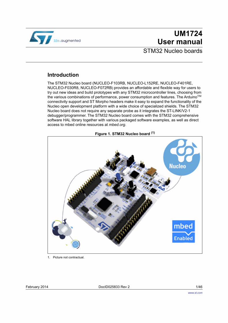
IntroductionThe STM32 Nucleo board (NUCLEO-F103RB, NUCLEO-L152RE, NUCLEO-F401RE, NUCLEO-F030R8, NUCLEO-F072RB) provides an affordable and flexible way for users to try out new ideas and build prototypes with any STM32 microcontroller lines, choosing from the various combinations of performance, power consumption and features. The ArduinoΤΜ connectivity support and ST Morpho headers make it easy to expand the functionality of the Nucleo open development platform with a wide choice of specialized shields. The STM32 Nucleo board does not require any separate probe as it integrates the ST-LINK/V2-1 debugger/programmer. The STM32 Nucleo board comes with the STM32 comprehensive software HAL library together with various packaged software examples, as well as direct access to mbed online resources at mbed.org.
Figure 1. STM32 Nucleo board (1)
1. Picture not contractual.
www.st.com
Contents UM1724
2/46 DocID025833 Rev 2
Contents
1 Ordering information . . . . . . . . . . . . . . . . . . . . . . . . . . . . . . . . . . . . . . . . 6
2 Conventions . . . . . . . . . . . . . . . . . . . . . . . . . . . . . . . . . . . . . . . . . . . . . . . 7
3 Quick start . . . . . . . . . . . . . . . . . . . . . . . . . . . . . . . . . . . . . . . . . . . . . . . . . 83.1 Getting started . . . . . . . . . . . . . . . . . . . . . . . . . . . . . . . . . . . . . . . . . . . . . . 8
3.2 System requirements . . . . . . . . . . . . . . . . . . . . . . . . . . . . . . . . . . . . . . . . . 8
4 Features . . . . . . . . . . . . . . . . . . . . . . . . . . . . . . . . . . . . . . . . . . . . . . . . . . . 9
5 Hardware layout and configuration . . . . . . . . . . . . . . . . . . . . . . . . . . . . 105.1 Cutable PCB . . . . . . . . . . . . . . . . . . . . . . . . . . . . . . . . . . . . . . . . . . . . . . . 12
5.2 Embedded ST-LINK/V2-1 . . . . . . . . . . . . . . . . . . . . . . . . . . . . . . . . . . . . . 135.2.1 Drivers . . . . . . . . . . . . . . . . . . . . . . . . . . . . . . . . . . . . . . . . . . . . . . . . . 14
5.2.2 ST-LINK/V2-1 firmware upgrade . . . . . . . . . . . . . . . . . . . . . . . . . . . . . . 14
5.2.3 Using the ST-LINK/V2-1 to program/debug the STM32 on board . . . . 14
5.2.4 Using ST-LINK/V2-1 to program/debug an external STM32 application 15
5.3 Power supply and power selection . . . . . . . . . . . . . . . . . . . . . . . . . . . . . . 165.3.1 Power supply input from the USB connector . . . . . . . . . . . . . . . . . . . . . 16
5.3.2 External power supply inputs: VIN and EV5 . . . . . . . . . . . . . . . . . . . . . 17
5.3.3 External power supply input: + 3V3 . . . . . . . . . . . . . . . . . . . . . . . . . . . . 19
5.3.4 External power supply output . . . . . . . . . . . . . . . . . . . . . . . . . . . . . . . . 19
5.4 LEDs . . . . . . . . . . . . . . . . . . . . . . . . . . . . . . . . . . . . . . . . . . . . . . . . . . . . . 19
5.5 Push buttons . . . . . . . . . . . . . . . . . . . . . . . . . . . . . . . . . . . . . . . . . . . . . . 20
5.6 JP6 (IDD) . . . . . . . . . . . . . . . . . . . . . . . . . . . . . . . . . . . . . . . . . . . . . . . . . 20
5.7 OSC clock . . . . . . . . . . . . . . . . . . . . . . . . . . . . . . . . . . . . . . . . . . . . . . . . 215.7.1 OSC clock supply . . . . . . . . . . . . . . . . . . . . . . . . . . . . . . . . . . . . . . . . . 21
5.7.2 OSC 32 kHz clock supply . . . . . . . . . . . . . . . . . . . . . . . . . . . . . . . . . . . 22
5.8 USART communication . . . . . . . . . . . . . . . . . . . . . . . . . . . . . . . . . . . . . . 22
5.9 Solder bridges . . . . . . . . . . . . . . . . . . . . . . . . . . . . . . . . . . . . . . . . . . . . . 23
5.10 Extension connectors . . . . . . . . . . . . . . . . . . . . . . . . . . . . . . . . . . . . . . . . 25
5.11 Arduino connectors . . . . . . . . . . . . . . . . . . . . . . . . . . . . . . . . . . . . . . . . . . 28
5.12 STMicroelectronics Morpho connector . . . . . . . . . . . . . . . . . . . . . . . . . . 35
DocID025833 Rev 2 3/46
UM1724 Contents
3
6 Mechanical drawing . . . . . . . . . . . . . . . . . . . . . . . . . . . . . . . . . . . . . . . . 40
7 Electrical schematics . . . . . . . . . . . . . . . . . . . . . . . . . . . . . . . . . . . . . . . 41
8 References . . . . . . . . . . . . . . . . . . . . . . . . . . . . . . . . . . . . . . . . . . . . . . . . 45
9 Revision history . . . . . . . . . . . . . . . . . . . . . . . . . . . . . . . . . . . . . . . . . . . 45
List of tables UM1724
4/46 DocID025833 Rev 2
List of tables
Table 1. Ordering information . . . . . . . . . . . . . . . . . . . . . . . . . . . . . . . . . . . . . . . . . . . . . . . . . . . . . . . 6Table 2. ON/OFF conventions . . . . . . . . . . . . . . . . . . . . . . . . . . . . . . . . . . . . . . . . . . . . . . . . . . . . . . 7Table 3. Jumper states . . . . . . . . . . . . . . . . . . . . . . . . . . . . . . . . . . . . . . . . . . . . . . . . . . . . . . . . . . . 13Table 4. Debug connector CN4 (SWD). . . . . . . . . . . . . . . . . . . . . . . . . . . . . . . . . . . . . . . . . . . . . . . 15Table 5. JP1 configuration table . . . . . . . . . . . . . . . . . . . . . . . . . . . . . . . . . . . . . . . . . . . . . . . . . . . . 17Table 6. External power sources . . . . . . . . . . . . . . . . . . . . . . . . . . . . . . . . . . . . . . . . . . . . . . . . . . . 17Table 7. Power-related jumper . . . . . . . . . . . . . . . . . . . . . . . . . . . . . . . . . . . . . . . . . . . . . . . . . . . . . 18Table 8. +3.3V eternal power source . . . . . . . . . . . . . . . . . . . . . . . . . . . . . . . . . . . . . . . . . . . . . . . . 19Table 9. Solder bridges. . . . . . . . . . . . . . . . . . . . . . . . . . . . . . . . . . . . . . . . . . . . . . . . . . . . . . . . . . . 23Table 10. Arduino connectors on NUCLEO-F103RB . . . . . . . . . . . . . . . . . . . . . . . . . . . . . . . . . . . . . 29Table 11. Arduino connectors on NUCLEO-L152RE . . . . . . . . . . . . . . . . . . . . . . . . . . . . . . . . . . . . . 30Table 12. Arduino connectors on NUCLEO-F401RE . . . . . . . . . . . . . . . . . . . . . . . . . . . . . . . . . . . . . 32Table 13. Arduino connectors on NUCLEO-F030R8, NUCLEO-F072RB. . . . . . . . . . . . . . . . . . . . . . 33Table 14. STMicroelectronics Morpho connector on NUCLEO-F103RB . . . . . . . . . . . . . . . . . . . . . . 35Table 15. STMicroelectronics Morpho connector on NUCLEO-L152RE . . . . . . . . . . . . . . . . . . . . . . 36Table 16. STMicroelectronics Morpho connector on NUCLEO-F401RE . . . . . . . . . . . . . . . . . . . . . . 37Table 17. STMicroelectronics Morpho connector on NUCLEO-F030R8 . . . . . . . . . . . . . . . . . . . . . . 38Table 18. STMicroelectronics Morpho connector on NUCLEO-F072RB . . . . . . . . . . . . . . . . . . . . . . 39Table 19. Document revision history. . . . . . . . . . . . . . . . . . . . . . . . . . . . . . . . . . . . . . . . . . . . . . . . . . 45
DocID025833 Rev 2 5/46
UM1724 List of figures
5
List of figures
Figure 1. STM32 Nucleo board (1) . . . . . . . . . . . . . . . . . . . . . . . . . . . . . . . . . . . . . . . . . . . . . . . . . . . . 1Figure 2. Hardware block diagram . . . . . . . . . . . . . . . . . . . . . . . . . . . . . . . . . . . . . . . . . . . . . . . . . . 10Figure 3. Top layout . . . . . . . . . . . . . . . . . . . . . . . . . . . . . . . . . . . . . . . . . . . . . . . . . . . . . . . . . . . . . . 11Figure 4. Bottom layout . . . . . . . . . . . . . . . . . . . . . . . . . . . . . . . . . . . . . . . . . . . . . . . . . . . . . . . . . . . 12Figure 5. Typical configuration. . . . . . . . . . . . . . . . . . . . . . . . . . . . . . . . . . . . . . . . . . . . . . . . . . . . . . 13Figure 6. Updating the list of drivers in Device Manager . . . . . . . . . . . . . . . . . . . . . . . . . . . . . . . . . . 14Figure 7. Connecting the STM32 Nucleo board to program the on-board STM32 . . . . . . . . . . . . . . 15Figure 8. Using ST-LINK/V2-1 to program the STM32 on an external application . . . . . . . . . . . . . . 16Figure 9. NUCLEO-F103RB. . . . . . . . . . . . . . . . . . . . . . . . . . . . . . . . . . . . . . . . . . . . . . . . . . . . . . . . 25Figure 10. NUCLEO-L152RE. . . . . . . . . . . . . . . . . . . . . . . . . . . . . . . . . . . . . . . . . . . . . . . . . . . . . . . . 26Figure 11. NUCLEO-F401RE. . . . . . . . . . . . . . . . . . . . . . . . . . . . . . . . . . . . . . . . . . . . . . . . . . . . . . . . 26Figure 12. NUCLEO-F030R8. . . . . . . . . . . . . . . . . . . . . . . . . . . . . . . . . . . . . . . . . . . . . . . . . . . . . . . . 27Figure 13. NUCLEO-F072RB. . . . . . . . . . . . . . . . . . . . . . . . . . . . . . . . . . . . . . . . . . . . . . . . . . . . . . . . 27Figure 14. STM32 Nucleo board mechanical drawing . . . . . . . . . . . . . . . . . . . . . . . . . . . . . . . . . . . . . 40Figure 15. Schematic (1/4) . . . . . . . . . . . . . . . . . . . . . . . . . . . . . . . . . . . . . . . . . . . . . . . . . . . . . . . . . 41Figure 16. Schematic (2/4). . . . . . . . . . . . . . . . . . . . . . . . . . . . . . . . . . . . . . . . . . . . . . . . . . . . . . . . . . 42Figure 17. Schematic (3/4) . . . . . . . . . . . . . . . . . . . . . . . . . . . . . . . . . . . . . . . . . . . . . . . . . . . . . . . . . 43Figure 18. Schematic (4/4) . . . . . . . . . . . . . . . . . . . . . . . . . . . . . . . . . . . . . . . . . . . . . . . . . . . . . . . . . 44
Ordering information UM1724
6/46 DocID025833 Rev 2
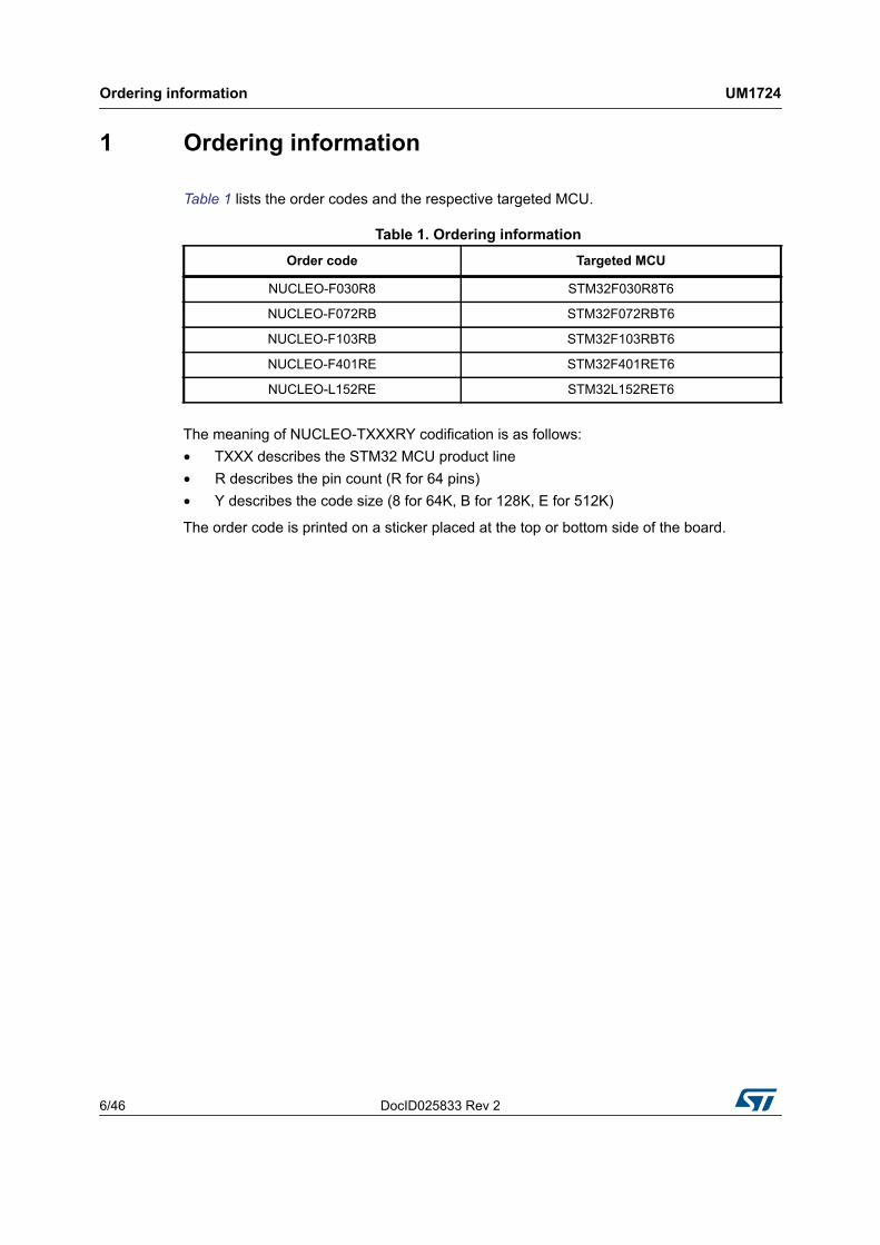
1 Ordering information
Table 1 lists the order codes and the respective targeted MCU.
The meaning of NUCLEO-TXXXRY codification is as follows:• TXXX describes the STM32 MCU product line• R describes the pin count (R for 64 pins)• Y describes the code size (8 for 64K, B for 128K, E for 512K)
The order code is printed on a sticker placed at the top or bottom side of the board.
Table 1. Ordering information Order code Targeted MCU
NUCLEO-F030R8 STM32F030R8T6
NUCLEO-F072RB STM32F072RBT6
NUCLEO-F103RB STM32F103RBT6
NUCLEO-F401RE STM32F401RET6
NUCLEO-L152RE STM32L152RET6
DocID025833 Rev 2 7/46
UM1724 Conventions
45
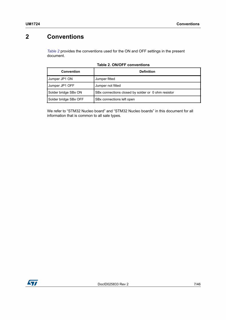
2 Conventions
Table 2 provides the conventions used for the ON and OFF settings in the present document.
We refer to “STM32 Nucleo board” and “STM32 Nucleo boards” in this document for all information that is common to all sale types.
Table 2. ON/OFF conventions Convention Definition
Jumper JP1 ON Jumper fitted
Jumper JP1 OFF Jumper not fitted
Solder bridge SBx ON SBx connections closed by solder or 0 ohm resistor
Solder bridge SBx OFF SBx connections left open
Quick start UM1724
8/46 DocID025833 Rev 2
3 Quick start
The STM32 Nucleo board is a low-cost and easy-to-use development platform used to quickly evaluate and start a development with an STM32 microcontroller in LQFP64 package.
Before installing and using the product, please accept the Evaluation Product License Agreement from www.st.com/epla.
For more information on the STM32 Nucleo boards and to access the demonstration software, visit www.st.com/stm32nucleo.
3.1 Getting startedFollow the sequence below to configure the STM32 Nucleo board and launch the demo software:1. Check the jumper position on the board, JP1 off, JP5 (PWR) on U5V, JP6 on (IDD),
CN2 on (NUCLEO) selected.2. Install the Nucleo USB driver available on www.st.com, prior to connecting the board.3. Connect the STM32 Nucleo board to a PC with a USB cable ‘type A to mini-B’ through
USB connector CN1 to power the board. The red LED LD3 (PWR) and LD1 (COM) should light up. LD1 (COM) and green LED LD2 should blink.
4. Press button B1 (left button).5. Observe how the blinking of the green LED LD2 changes according to clicks on button
B1.6. The demo software and several software examples on how use the STM32 Nucleo
board features are available on www.st.com/stm32nucleo.7. Develop your own application using the available examples.
3.2 System requirements• Windows PC (XP, Vista, 7, 8)• USB type A to Mini-B USB cable
DocID025833 Rev 2 9/46
UM1724 Features
45
4 Features
The STM32 Nucleo boards offer the following features:• STM32 microcontroller with LQFP64 package • Two types of extension resources
– Arduino Uno Revision 3 connectivity– STMicroelectronics Morpho extension pin headers for full access to all STM32 I/Os
• mbed-enabled(a)
• On-board ST-LINK/V2-1 debugger/programmer with SWD connector– selection-mode switch to use the kit as a standalone ST-LINK/V2-1
• Flexible board power supply– USB VBUS– External VIN (7V<VIN<12V) supply voltage from Arduino connectors or ST
Morpho connector– External 5V (E5V) supply voltage from ST Morpho connector– External +3.3V supply voltage from Arduino connector or ST Morpho connector
• Three LEDs– USB communication (LD1), user LED (LD2), power LED (LD3)
• Two push buttons: USER and RESET • USB re-enumeration capability: three different interfaces supported on USB
– Virtual Com port– Mass storage– Debug port
• Comprehensive free software HAL library including a variety of software examples• Supported by wide choice of Integrated Development Environments (IDEs) including IAR,
Keil, GCC-based IDEs
a. See http://mbed.org/
Hardware layout and configuration UM1724
10/46 DocID025833 Rev 2
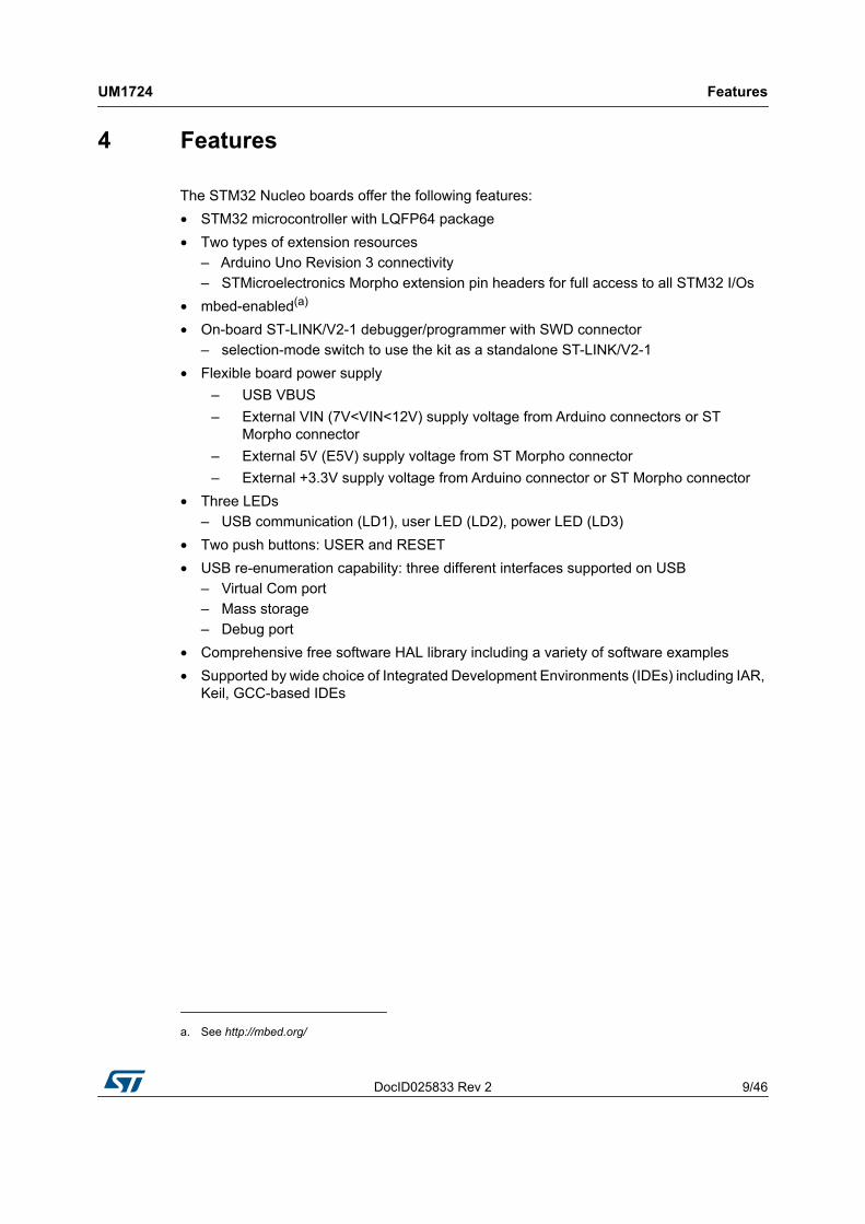
5 Hardware layout and configuration
The STM32 Nucleo board is designed around the STM32 microcontrollers in a 64-pin LQFP package.
Figure 2 shows the connections between the STM32 and its peripherals (STLINK/ V2-1, pushbutton, LED, Arduino connectors and STMicroelectronics Morpho connector).
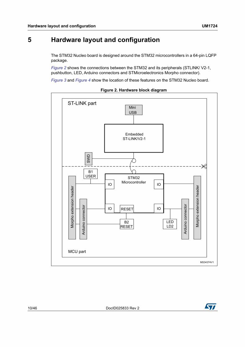
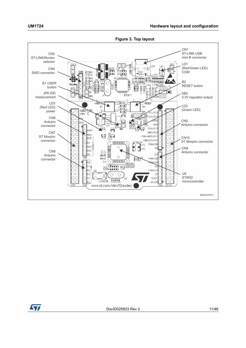
Figure 3 and Figure 4 show the location of these features on the STM32 Nucleo board.
Figure 2. Hardware block diagram
DocID025833 Rev 2 11/46
UM1724 Hardware layout and configuration
45
Figure 3. Top layout
Hardware layout and configuration UM1724
12/46 DocID025833 Rev 2
Figure 4. Bottom layout
5.1 Cutable PCBThe STM32 Nucleo board is divided into two parts: ST-LINK part and target MCU part. The ST-LINK part of the PCB can be cut out to reduce the board size. In this case the remaining target MCU part can only be powered by VIN, E5V and 3.3V on STMicroelectronics Morpho connector CN7 or VIN and 3.3V on Arduino connector CN6. It is still possible to use the ST-LINK part to program the main MCU using wires between CN4 and SWD signals available on STMicroelectronics Morpho connector (SWCLK CN7 pin 15 and SWDIO CN7 pin 13).
DocID025833 Rev 2 13/46
UM1724 Hardware layout and configuration
45
5.2 Embedded ST-LINK/V2-1The ST-LINK/V2-1 programming and debugging tool is integrated in the STM32 Nucleo boards.
The ST-LINK/V2-1 makes the STM32 Nucleo boards mbed enabled.
The embedded ST-LINK/V2-1 supports only SWD for STM32 devices. For information about debugging and programming features refer to UM1075 - ST-LINK/V2 in-circuit debugger/programmer for STM8 and STM32, User manual, which describes in detail all the ST-LINK/V2 features.
The changes versus ST-LINK/V2 version are listed below.• New features supported on ST-LINK/V2-1:
– USB software re-enumeration– Virtual com port interface on USB– Mass storage interface on USB– USB power management request for more than 100 mA power on USB
• Features not supported on ST-LINK/V2-1:– SWIM interface – Minimum supported application voltage limited to 3 V
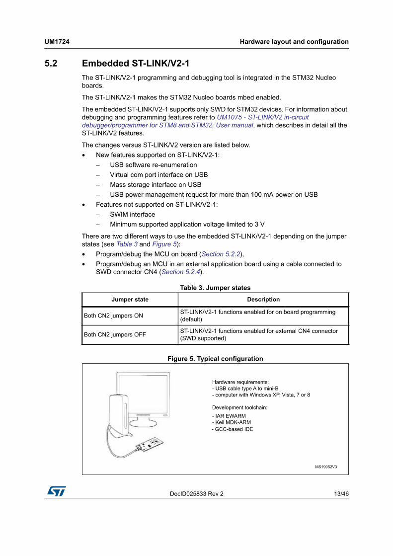
There are two different ways to use the embedded ST-LINK/V2-1 depending on the jumper states (see Table 3 and Figure 5):• Program/debug the MCU on board (Section 5.2.2),• Program/debug an MCU in an external application board using a cable connected to
SWD connector CN4 (Section 5.2.4).
Figure 5. Typical configuration
Table 3. Jumper statesJumper state Description
Both CN2 jumpers ON ST-LINK/V2-1 functions enabled for on board programming (default)
Both CN2 jumpers OFF ST-LINK/V2-1 functions enabled for external CN4 connector (SWD supported)
Hardware layout and configuration UM1724
14/46 DocID025833 Rev 2
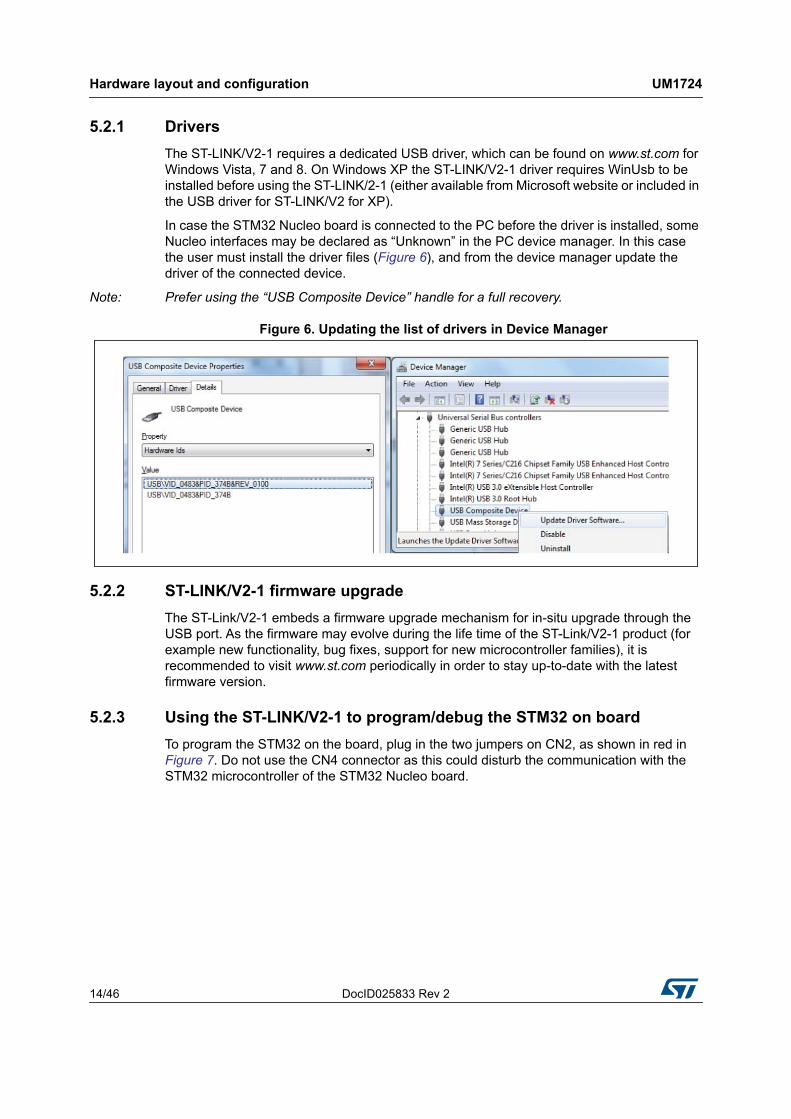
5.2.1 Drivers The ST-LINK/V2-1 requires a dedicated USB driver, which can be found on www.st.com for Windows Vista, 7 and 8. On Windows XP the ST-LINK/V2-1 driver requires WinUsb to be installed before using the ST-LINK/2-1 (either available from Microsoft website or included in the USB driver for ST-LINK/V2 for XP).
In case the STM32 Nucleo board is connected to the PC before the driver is installed, some Nucleo interfaces may be declared as “Unknown” in the PC device manager. In this case the user must install the driver files (Figure 6), and from the device manager update the driver of the connected device.
Note: Prefer using the “USB Composite Device” handle for a full recovery.
Figure 6. Updating the list of drivers in Device Manager
5.2.2 ST-LINK/V2-1 firmware upgradeThe ST-Link/V2-1 embeds a firmware upgrade mechanism for in-situ upgrade through the USB port. As the firmware may evolve during the life time of the ST-Link/V2-1 product (for example new functionality, bug fixes, support for new microcontroller families), it is recommended to visit www.st.com periodically in order to stay up-to-date with the latest firmware version.
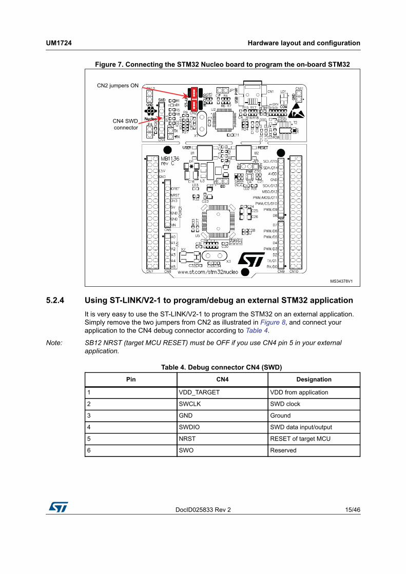
5.2.3 Using the ST-LINK/V2-1 to program/debug the STM32 on board To program the STM32 on the board, plug in the two jumpers on CN2, as shown in red in Figure 7. Do not use the CN4 connector as this could disturb the communication with the STM32 microcontroller of the STM32 Nucleo board.
DocID025833 Rev 2 15/46
UM1724 Hardware layout and configuration
45
Figure 7. Connecting the STM32 Nucleo board to program the on-board STM32
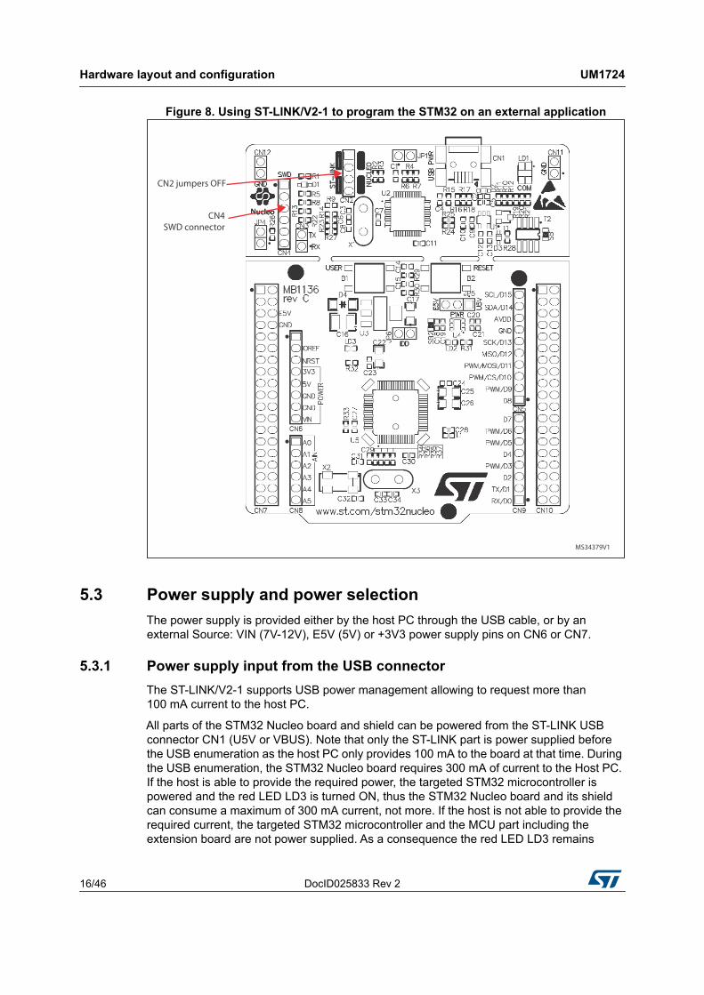
5.2.4 Using ST-LINK/V2-1 to program/debug an external STM32 applicationIt is very easy to use the ST-LINK/V2-1 to program the STM32 on an external application. Simply remove the two jumpers from CN2 as illustrated in Figure 8, and connect your application to the CN4 debug connector according to Table 4.
Note: SB12 NRST (target MCU RESET) must be OFF if you use CN4 pin 5 in your external application.
Table 4. Debug connector CN4 (SWD) Pin CN4 Designation
1 VDD_TARGET VDD from application
2 SWCLK SWD clock
3 GND Ground
4 SWDIO SWD data input/output
5 NRST RESET of target MCU
6 SWO Reserved
Hardware layout and configuration UM1724
16/46 DocID025833 Rev 2
Figure 8. Using ST-LINK/V2-1 to program the STM32 on an external application
5.3 Power supply and power selectionThe power supply is provided either by the host PC through the USB cable, or by an external Source: VIN (7V-12V), E5V (5V) or +3V3 power supply pins on CN6 or CN7.
5.3.1 Power supply input from the USB connectorThe ST-LINK/V2-1 supports USB power management allowing to request more than 100 mA current to the host PC.
All parts of the STM32 Nucleo board and shield can be powered from the ST-LINK USB connector CN1 (U5V or VBUS). Note that only the ST-LINK part is power supplied before the USB enumeration as the host PC only provides 100 mA to the board at that time. During the USB enumeration, the STM32 Nucleo board requires 300 mA of current to the Host PC. If the host is able to provide the required power, the targeted STM32 microcontroller is powered and the red LED LD3 is turned ON, thus the STM32 Nucleo board and its shield can consume a maximum of 300 mA current, not more. If the host is not able to provide the required current, the targeted STM32 microcontroller and the MCU part including the extension board are not power supplied. As a consequence the red LED LD3 remains
DocID025833 Rev 2 17/46
UM1724 Hardware layout and configuration
45
turned OFF. In such case it is mandatory to use an external power supply as explained in the next chapter.
When the board is power supplied by USB (U5V) a jumper must be connected between pin 1 and pin 2 of JP5 as shown in Table 7.
JP1 is configured according to the maximum current consumption of the board when powered by USB (U5V). JP1 jumper can be set only in case the board is powered by USB and maximum current consumption on U5V doesn’t exceed 100mA (including an eventual extension board or Arduino Shield). In such condition USB enumeration will always succeed since no more than 100mA is requested to the PC. Possible configurations of JP1 are summarized in Table 5.
Warning: If the maximum current consumption of the NUCLEO and its extension boards exceeds 300 mA, it is mandatory to power the NUCLEO using an external power supply connected to E5V or VIN.
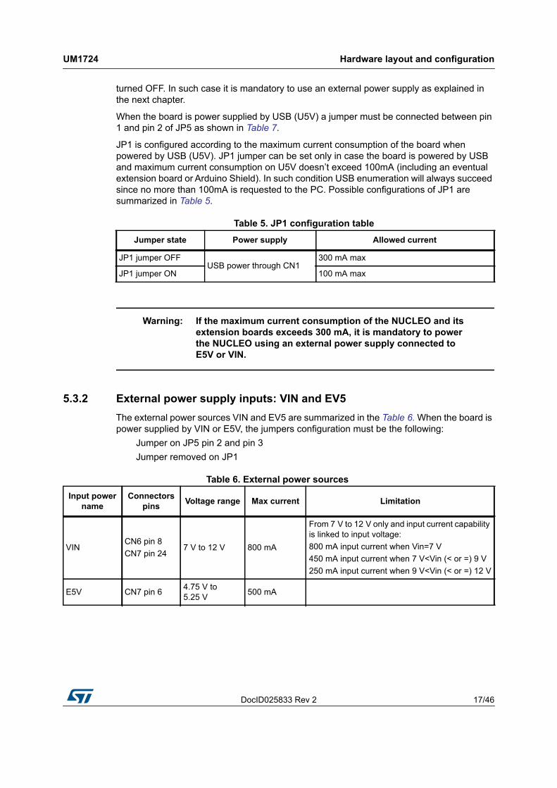
5.3.2 External power supply inputs: VIN and EV5The external power sources VIN and EV5 are summarized in the Table 6. When the board is power supplied by VIN or E5V, the jumpers configuration must be the following:
Jumper on JP5 pin 2 and pin 3Jumper removed on JP1
Table 5. JP1 configuration table Jumper state Power supply Allowed current
JP1 jumper OFFUSB power through CN1
300 mA max
JP1 jumper ON 100 mA max
Table 6. External power sources Input power
nameConnectors
pins Voltage range Max current Limitation
VINCN6 pin 8 CN7 pin 24
7 V to 12 V 800 mA
From 7 V to 12 V only and input current capability is linked to input voltage:800 mA input current when Vin=7 V450 mA input current when 7 V<Vin (< or =) 9 V250 mA input current when 9 V<Vin (< or =) 12 V
E5V CN7 pin 6 4.75 V to 5.25 V 500 mA
Hardware layout and configuration UM1724
18/46 DocID025833 Rev 2
Using VIN or E5V as external power supply
VIN or E5V can be used as external power supply in case the current consumption of NUCLEO and extensions boards exceeds the allowed current on USB. In this condition it is still possible to use the USB for communication, for programming or debugging only, but it is mandatory to power supply the board first using VIN or E5V then connect the USB cable to the PC. Proceeding this way ensures that the enumeration occurs thanks to the external power source.
The following power sequence procedure must be respected: 1. Connect the jumper between pin 2 and pin 3 of JP5. 2. Check that JP1 is removed.3. Connect the external power source to VIN or E5V.4. Power on the external power supply 7 V< VIN < 12 V to VIN, or 5 V for E5V.5. Check that LD3 is turned ON.6. Connect the PC to USB connector CN1.
If this order is not respected, the board may be supplied by VBUS first then by VIN or E5V, and the following risks may be encountered:1. If more than 300 mA current is needed by the board, the PC may be damaged or the
current supply can be limited by the PC. As a consequence the board is not powered correctly.
2. 300 mA is requested at enumeration (since JP1 must be OFF) so there is risk that the request is rejected and the enumeration does not succeed if the PC cannot provide such current. Consequently the board is not power supplied (LED LD3 remains OFF).
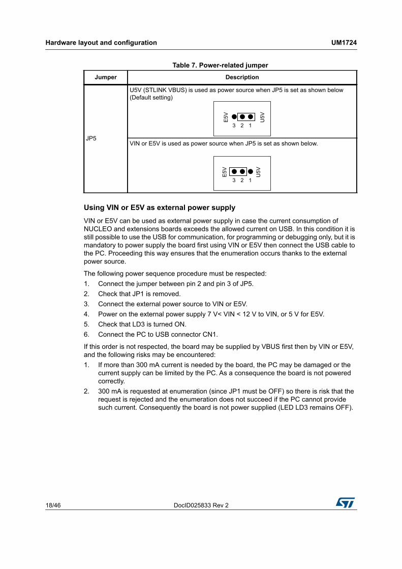
Table 7. Power-related jumperJumper Description
JP5
U5V (STLINK VBUS) is used as power source when JP5 is set as shown below (Default setting)
VIN or E5V is used as power source when JP5 is set as shown below.
DocID025833 Rev 2 19/46
UM1724 Hardware layout and configuration
45
5.3.3 External power supply input: + 3V3It can be of interest to use the +3V3 (CN6 pin 4 or CN7 pin 12 and pin 16) directly as power input for instance in case the 3.3 V is provided by an extension board. When NUCLEO is power supplied by +3V3, the ST-LINK is not powered thus the programming and debug features are unavailable. The external power sources +3.3V is summarized in the Table 8.
Two different configurations are possible to use +3V3 to power the board:• ST-LINK is removed (PCB cut), or• SB2 (3V3 regulator) & SB12 (NRST) are OFF.
5.3.4 External power supply outputWhen powered by USB, VIN or E5V, the +5V (CN6 pin 5 or CN7 pin 18) can be used as output power supply for an Arduino shield or an extension board. In this case, the maximum current of the power source specified in Table 6 needs to be respected.
The +3.3 V (CN6 pin 4 or CN7 pin 12 & 16) can be used also as power supply output. The current is limited by the maximum current capability of the regulator U4 (500 mA max).
5.4 LEDsThe tricolor LED (green, orange, red) LD1 (COM) provides information about ST-LINK communication status. LD1 default color is red. LD1 turns to green to indicate that communication is in progress between the PC and the ST-LINK/V2-1, with the following setup:• Slow blinking Red/Off: at power-on before USB initialization• Fast blinking Red/Off: after the first correct communication between the PC and ST-
LINK/V2-1 (enumeration)• Red LED On: when the initialization between the PC and ST-LINK/V2-1 is complete • Green LED On: after a successful target communication initialization• Blinking Red/Green: during communication with target• Green On: communication finished and successful.• Orange On: Communication failure
User LD2: the green LED is a user LED connected to Arduino signal D13 corresponding to MCU I/O PA5 (pin 21) or PB13 (pin 34) depending on the STM32 target. Please refer to Table 10 to Table 13. • When the I/O is HIGH value, the LED is on.• When the I/O is LOW, the LED is off.
LD3 PWR: the red LED indicates that the MCU part is powered and +5V power is available.
Table 8. +3.3V eternal power source Input power
name Connectors pins Voltage range Limitation
+3V3CN6 pin 4CN7 pin 12 and pin 16
3 V to 3.6 V Used when ST-LINK part of PCB is cut or SB2 and SB12 OFF
Hardware layout and configuration UM1724
20/46 DocID025833 Rev 2
5.5 Push buttonsB1 USER: the user (or wake-up) button is connected to the I/O PC13 (pin 2) of the STM32 microcontroller.
B2 RESET: this push button is connected to NRST, and is used to RESET the STM32 microcontroller.
Note: The blue and black plastic hats that are placed on the push buttons can be removed if necessary, for example when a shield or when an application board is plugged on top of NUCLEO. This will avoid pressure on the buttons and consequently a possible permanent target MCU RESET.
5.6 JP6 (IDD)Jumper JP6, labeled IDD, is used to measure the STM32 microcontroller consumption by removing the jumper and by connecting an ammeter.• Jumper ON: STM32 microcontroller is powered (default).• Jumper OFF: an ammeter must be connected to measure the STM32 microcontroller
current. If there is no ammeter, STM32 microcontroller is not powered.
DocID025833 Rev 2 21/46
UM1724 Hardware layout and configuration
45
5.7 OSC clock
5.7.1 OSC clock supplyThere are three ways to manage the external high-speed clock (HSE):• MCO from ST-LINK: from MCO of the ST-LINK MCU (U2 on schematic). This
frequency cannot be changed, it is fixed at 8 MHz and connected to PF0/PD0/PH0-OSC_IN of STM32 microcontroller. The following configuration is needed:– SB54, SB55 OFF– R35,R37 removed– SB16, SB50 ON
• HSE oscillator on-board from X3 crystal (not provided): for typical frequencies and its capacitors and resistors, please refer to STM32 microcontroller datasheet. The X3 crystal has the following characteristics: 8 MHz, 16PF, 20PPM, and DIP footprint.
The following configuration is needed:– SB54, SB55 OFF– R35, R37 soldered– C33, C34 soldered with 20pF capacitors– SB16, SB50 OFF
• Oscillator from external PF0/PD0/PH0: from an external oscillator through pin 29 of the CN7 connector. The following configuration is needed:– SB55 ON– SB50 OFF– R35,R37 removedIf PF0/PD0/PH0 and PF1/PD1/PH1 are used as GPIOs instead being used as a clock:– SB54 and SB55 are ON, – R35 and R37 are removed, and– SB50 (MCO) is OFF (default configuration).
Part number example: 9SL8000016AFXHF0
Manufacturer: Hong Kong X'tals Limited
Website: http://www.hongkongcrystal.com/en/index.php
Hardware layout and configuration UM1724
22/46 DocID025833 Rev 2
5.7.2 OSC 32 kHz clock supplyThere are two ways to manage the external low-speed clock (LSE):• On-board oscillator (not provided): X2 crystal with the following characteristics:
32.768 kHz, 2.5PF, 20PPM, and SM308 footprint
The following configuration is needed:– SB48, SB49 OFF– R34 and R36 soldered.– C31, C32 soldered with 10pF capacitors
Oscillator from external PC14: from external oscillator through the pin 25 of CN7connector.
The following configuration is needed:– SB48, SB49 ON– R34 and R36 removedIf PC14 and PC15 are used as GPIOs instead of being used as clock:– SB48 and SB49 are ON, and – R34 and R36 are removed (default configuration).
5.8 USART communicationThe USART interface of STM32 microcontroller on STM32 Nucleo board can be connected to ST-LINK MCU, or STMicroelectronics Morpho connector or to Arduino connector. The choice can be changed by setting the related solder bridges. By default the USART communication between the target MCU and ST-LINK MCU is enabled in order to support Virtual Com Port for mbed (SB13 and SB14 ON, SB62 and SB63 OFF). If the communication between the target MCU and shield or extension board is required, SB62 and SB63 should be ON, SB13 and SB14 should be OFF.
Part number example: ETMB32.768B125B
Manufacturer: BEIJING JINGYUXING TECHNOLOGY Co., Ltd.
Website: http://en.jfvny.com/
DocID025833 Rev 2 23/46
UM1724 Hardware layout and configuration
45
5.9 Solder bridges
Table 9. Solder bridges
Bridge State(1) Description
SB54, SB55 (X3 crystal)(2)
OFF X3, C33, C34, R35 and R37 provide a clock as shown in Chapter 7: Electrical schematics PF0/PD0/PH0, PF1/PD1/PH1 are disconnected from CN7.
ON PF0/PD0/PH0, PF1/PD1/PH1 are connected to CN12. (R35, R37 and SB50 must not be fitted).
SB3,5,7,9 (DEFAULT) ON Reserved, do not modify.
SB4,6,8,10 (RESERVED) OFF Reserved, do not modify.
SB48,49 (X2 crystal)
OFF X2, C31, C32, R34 and R36 deliver a 32 kHz clock. PC14, PC15 are not connected to CN7.
ON PC14, PC15 are only connected to CN7. Remove only R34, R36
SB17(B1-USER)
ON B1 push button is connected to PC13.
OFF B1 push button is not connected to PC13.
SB12 (NRST)ON The NRST signal of the CN4 connector is connected to the NRST pin of the
STM32 MCU.
OFF The NRST signal of the CN4 connector is not connected to the NRST pin of the STM MCU.
SB15 (SWO)ON The SWO signal of the CN4 connector is connected to PB3.
OFF The SWO signal is not connected.
SB11 (STM_RST)OFF No incidence on STM32F103C8T6 (ST-LINK MCU) NRST signal.
ON STM32F103C8T6 (ST-LINK MCU) NRST signal is connected to GND.
SB1 (USB-5V) OFF USB power management is functional.
ON USB power management is disabled.
SB2 (3.3 V) ON Output of voltage regulator LD39050PU33R is connected to 3.3V.
OFF Output of voltage regulator LD39050PU33R is not connected.
SB21 (LD2-LED) ON Green user LED LD2 is connected to D13 of Arduino signal.
OFF Green user LED LD2 is not connected.
SB56,SB51 (A4 and A5) ON
PC1 and PC0 (ADC in) are connected to A4 and A5 (pin 5 and pin 6) on Arduino connector CN8 and ST Morpho connector CN7. Thus SB46 and SB52 should be OFF.
OFF PC1 and PC0 (ADC in) are disconnected to A4 and A5 (pin 5 and pin 6) on Arduino connector CN8 and ST Morpho connectorCN7.
SB46,SB52 (I2C on A4 and A5)
OFF PB9 and PB8 (I2C) are disconnected to A4 and A5 (pin 5 and pin 6) on Arduino connector CN8 and ST Morpho connector CN7.
ONPB9 and PB8 (I2C) are connected to A4 and A5 (pin 5 and pin 6) on Arduino connector CN8 and ST Morpho connector CN7 as I2C signals. Thus SB56 and SB51 should be OFF.
Hardware layout and configuration UM1724
24/46 DocID025833 Rev 2
All the other solder bridges present on the STM32 Nucleo board are used to configure several IOs and power supply pins for compatibility of features and pinout with STM32 MCU supported.
All STM32 Nucleo boards are delivered with the solder-bridges configured according to the target MCU supported.
SB45 (VBAT/VLCD) ON VBAT or VLCD on STM32 MCU is connected to VDD.
OFF VBAT or VLCD on STM32 MCU is not connected to VDD.
SB57 (VREF+)ON VREF+ on STM32 MCU is connected to VDD.
OFF VREF+ on STM32 MCU is not connected to VDD and can be provided from pin 7 of CN10
SB62, SB63 (USART)ON
PA2 and PA3 on STM32 MCU are connected to D1 and D0 (pin 7 and pin 8) on Arduino connector CN9 and ST Morpho connector CN10 as USART signals. Thus SB13 and SB14 should be OFF.
OFF PA2 and PA3 on STM32 MCU are disconnected to D1 and D0 (pin 7 and pin 8) on Arduino connector CN9 and ST Morpho connector CN10.
SB13, SB14 (STLINK-USART)
OFF PA2 and PA3 on STM32F103C8T6 (ST-LINK MCU) are disconnected to PA3 and PA2 on STM32 MCU.
ONPA2 and PA3 on STM32F103C8T6 (ST-LINK MCU) are connected to PA3 and PA2 on STM32 MCU to have USART communication between them. Thus SB61,SB62 and SB63 should be OFF.
SB16,SB50(MCO)OFF MCO on STM32F103C8T6 (ST-LINK MCU) are disconnected to PF0/PD0/PH0
on STM32 MCU.
ON MCO on STM32F103C8T6 (ST-LINK MCU) are connected to PF0/PD0/PH0 on STM32 MCU.
1. The default SBx state is shown in bold.
2. SB54 and SB55 are OFF to allow the user to choose between MCO and X3 crystal for the clock source.
Table 9. Solder bridges (continued)
Bridge State(1) Description
DocID025833 Rev 2 25/46
UM1724 Hardware layout and configuration
45
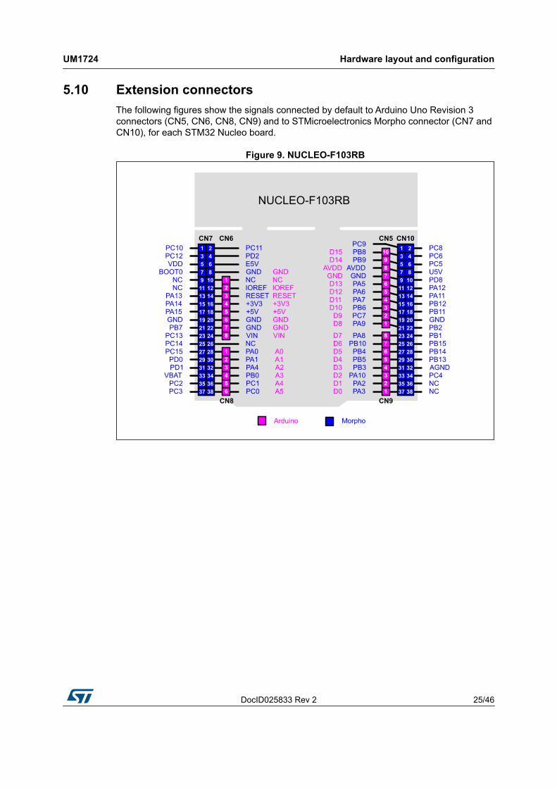
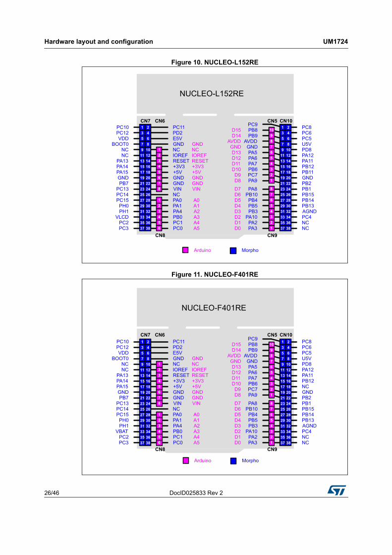
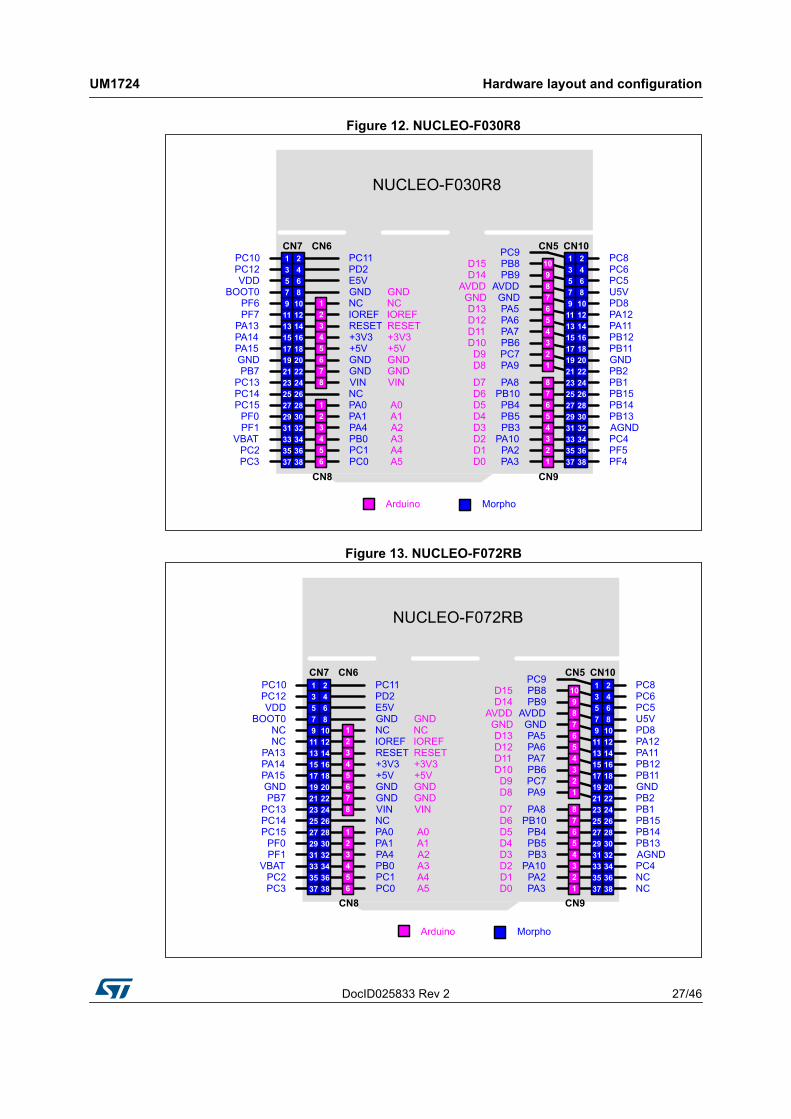
5.10 Extension connectorsThe following figures show the signals connected by default to Arduino Uno Revision 3 connectors (CN5, CN6, CN8, CN9) and to STMicroelectronics Morpho connector (CN7 and CN10), for each STM32 Nucleo board.
Figure 9. NUCLEO-F103RB
Hardware layout and configuration UM1724
26/46 DocID025833 Rev 2
Figure 10. NUCLEO-L152RE
Figure 11. NUCLEO-F401RE
DocID025833 Rev 2 27/46
UM1724 Hardware layout and configuration
45
Figure 12. NUCLEO-F030R8
Figure 13. NUCLEO-F072RB
Hardware layout and configuration UM1724
28/46 DocID025833 Rev 2
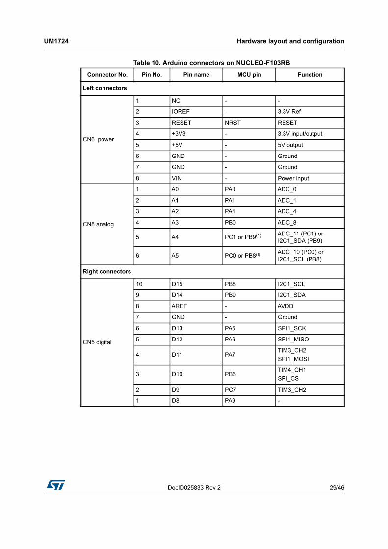
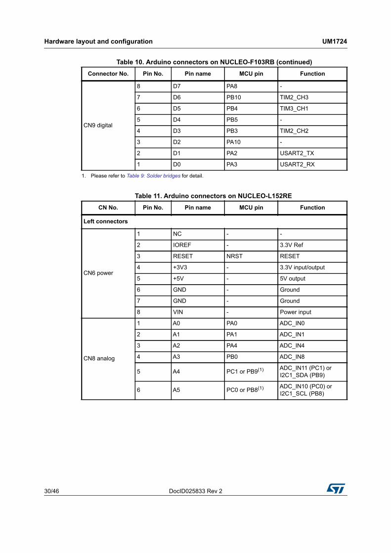
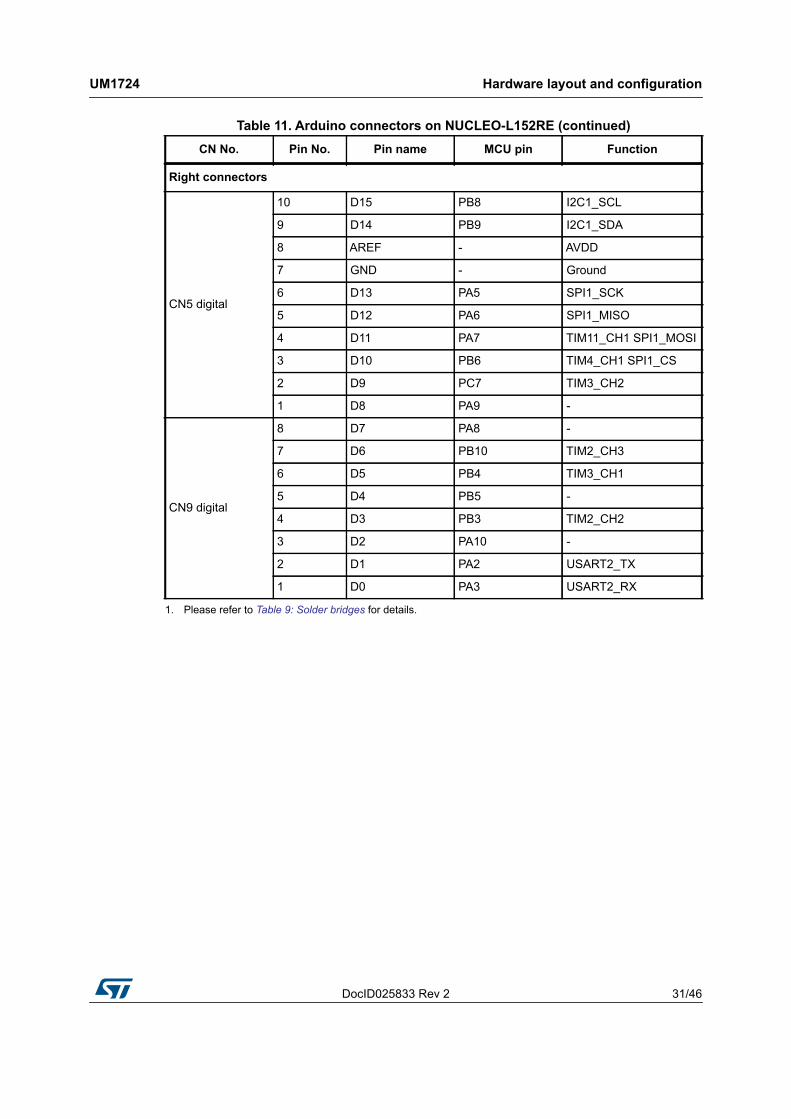
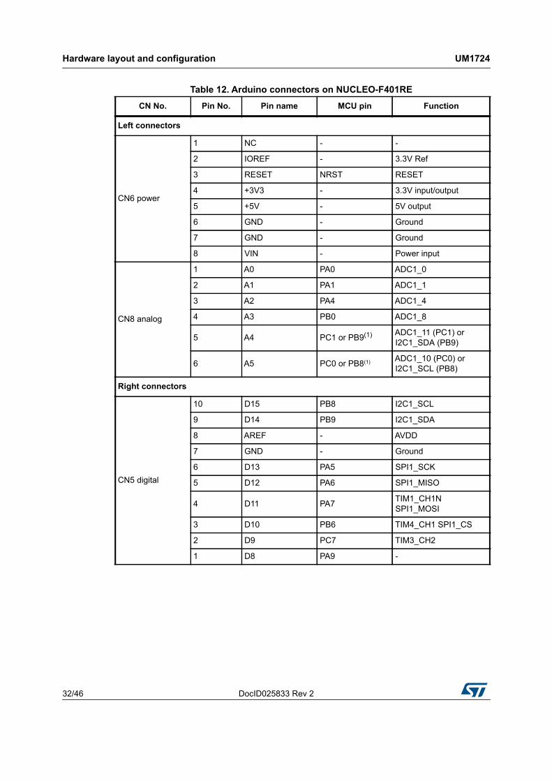
5.11 Arduino connectorsCN5, CN6, CN8 and CN9 are female connectors compatible with Arduino standard. Most shields designed for Arduino can fit to the STM32 Nucleo boards.
The Arduino connectors on STM32 Nucleo board support the Arduino Uno Revision 3.
For compatibility with Arduino Uno Revision 1, apply the following modifications:• SB46 and SB52 should be ON, • SB51 and SB56 should be OFF to connect I2C on A4 (pin 5) and A5 (pin 6 of CN8).
Caution: The IOs of STM32 microcontroller are 3.3 V compatible instead of 5 V for Arduino Uno.
Table 10 to Table 13 show the pin assignment of each main STM32 microcontroller on Arduino connectors.
DocID025833 Rev 2 29/46
UM1724 Hardware layout and configuration
45
Table 10. Arduino connectors on NUCLEO-F103RB Connector No. Pin No. Pin name MCU pin Function
Left connectors
CN6 power
1 NC - -
2 IOREF - 3.3V Ref
3 RESET NRST RESET
4 +3V3 - 3.3V input/output
5 +5V - 5V output
6 GND - Ground
7 GND - Ground
8 VIN - Power input
CN8 analog
1 A0 PA0 ADC_0
2 A1 PA1 ADC_1
3 A2 PA4 ADC_4
4 A3 PB0 ADC_8
5 A4 PC1 or PB9(1) ADC_11 (PC1) or I2C1_SDA (PB9)
6 A5 PC0 or PB8(1) ADC_10 (PC0) or I2C1_SCL (PB8)
Right connectors
CN5 digital
10 D15 PB8 I2C1_SCL
9 D14 PB9 I2C1_SDA
8 AREF - AVDD
7 GND - Ground
6 D13 PA5 SPI1_SCK
5 D12 PA6 SPI1_MISO
4 D11 PA7 TIM3_CH2 SPI1_MOSI
3 D10 PB6TIM4_CH1SPI_CS
2 D9 PC7 TIM3_CH2
1 D8 PA9 -
Hardware layout and configuration UM1724
30/46 DocID025833 Rev 2
CN9 digital
8 D7 PA8 -
7 D6 PB10 TIM2_CH3
6 D5 PB4 TIM3_CH1
5 D4 PB5 -
4 D3 PB3 TIM2_CH2
3 D2 PA10 -
2 D1 PA2 USART2_TX
1 D0 PA3 USART2_RX
1. Please refer to Table 9: Solder bridges for detail.
Table 11. Arduino connectors on NUCLEO-L152RE CN No. Pin No. Pin name MCU pin Function
Left connectors
CN6 power
1 NC - -
2 IOREF - 3.3V Ref
3 RESET NRST RESET
4 +3V3 - 3.3V input/output
5 +5V - 5V output
6 GND - Ground
7 GND - Ground
8 VIN - Power input
CN8 analog
1 A0 PA0 ADC_IN0
2 A1 PA1 ADC_IN1
3 A2 PA4 ADC_IN4
4 A3 PB0 ADC_IN8
5 A4 PC1 or PB9(1) ADC_IN11 (PC1) or I2C1_SDA (PB9)
6 A5 PC0 or PB8(1) ADC_IN10 (PC0) or I2C1_SCL (PB8)
Table 10. Arduino connectors on NUCLEO-F103RB (continued)Connector No. Pin No. Pin name MCU pin Function
DocID025833 Rev 2 31/46
UM1724 Hardware layout and configuration
45
Right connectors
CN5 digital
10 D15 PB8 I2C1_SCL
9 D14 PB9 I2C1_SDA
8 AREF - AVDD
7 GND - Ground
6 D13 PA5 SPI1_SCK
5 D12 PA6 SPI1_MISO
4 D11 PA7 TIM11_CH1 SPI1_MOSI
3 D10 PB6 TIM4_CH1 SPI1_CS
2 D9 PC7 TIM3_CH2
1 D8 PA9 -
CN9 digital
8 D7 PA8 -
7 D6 PB10 TIM2_CH3
6 D5 PB4 TIM3_CH1
5 D4 PB5 -
4 D3 PB3 TIM2_CH2
3 D2 PA10 -
2 D1 PA2 USART2_TX
1 D0 PA3 USART2_RX
1. Please refer to Table 9: Solder bridges for details.
Table 11. Arduino connectors on NUCLEO-L152RE (continued)CN No. Pin No. Pin name MCU pin Function
Hardware layout and configuration UM1724
32/46 DocID025833 Rev 2
Table 12. Arduino connectors on NUCLEO-F401RE CN No. Pin No. Pin name MCU pin Function
Left connectors
CN6 power
1 NC - -
2 IOREF - 3.3V Ref
3 RESET NRST RESET
4 +3V3 - 3.3V input/output
5 +5V - 5V output
6 GND - Ground
7 GND - Ground
8 VIN - Power input
CN8 analog
1 A0 PA0 ADC1_0
2 A1 PA1 ADC1_1
3 A2 PA4 ADC1_4
4 A3 PB0 ADC1_8
5 A4 PC1 or PB9(1) ADC1_11 (PC1) or I2C1_SDA (PB9)
6 A5 PC0 or PB8(1) ADC1_10 (PC0) or I2C1_SCL (PB8)
Right connectors
CN5 digital
10 D15 PB8 I2C1_SCL
9 D14 PB9 I2C1_SDA
8 AREF - AVDD
7 GND - Ground
6 D13 PA5 SPI1_SCK
5 D12 PA6 SPI1_MISO
4 D11 PA7 TIM1_CH1N SPI1_MOSI
3 D10 PB6 TIM4_CH1 SPI1_CS
2 D9 PC7 TIM3_CH2
1 D8 PA9 -
DocID025833 Rev 2 33/46
UM1724 Hardware layout and configuration
45
CN9 digital
8 D7 PA8 -
7 D6 PB10 TIM2_CH3
6 D5 PB4 TIM3_CH1
5 D4 PB5 -
4 D3 PB3 TIM2_CH2
3 D2 PA10 -
2 D1 PA2 USART2_TX
1 D0 PA3 USART2_RX
1. Please refer to Table 9: Solder bridges for details.
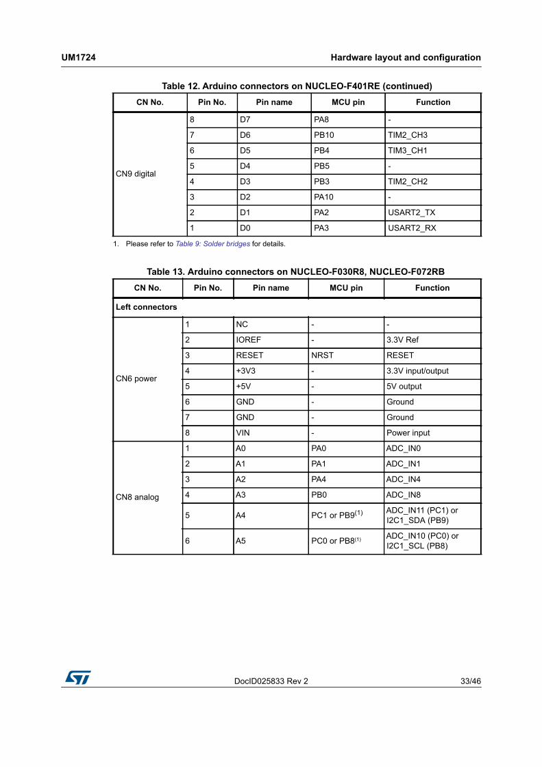
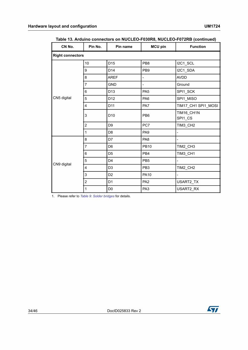
Table 13. Arduino connectors on NUCLEO-F030R8, NUCLEO-F072RB CN No. Pin No. Pin name MCU pin Function
Left connectors
CN6 power
1 NC - -
2 IOREF - 3.3V Ref
3 RESET NRST RESET
4 +3V3 - 3.3V input/output
5 +5V - 5V output
6 GND - Ground
7 GND - Ground
8 VIN - Power input
CN8 analog
1 A0 PA0 ADC_IN0
2 A1 PA1 ADC_IN1
3 A2 PA4 ADC_IN4
4 A3 PB0 ADC_IN8
5 A4 PC1 or PB9(1) ADC_IN11 (PC1) or I2C1_SDA (PB9)
6 A5 PC0 or PB8(1) ADC_IN10 (PC0) or I2C1_SCL (PB8)
Table 12. Arduino connectors on NUCLEO-F401RE (continued)CN No. Pin No. Pin name MCU pin Function
Hardware layout and configuration UM1724
34/46 DocID025833 Rev 2
Right connectors
CN5 digital
10 D15 PB8 I2C1_SCL
9 D14 PB9 I2C1_SDA
8 AREF - AVDD
7 GND - Ground
6 D13 PA5 SPI1_SCK
5 D12 PA6 SPI1_MISO
4 D11 PA7 TIM17_CH1 SPI1_MOSI
3 D10 PB6TIM16_CH1N SPI1_CS
2 D9 PC7 TIM3_CH2
1 D8 PA9 -
CN9 digital
8 D7 PA8 -
7 D6 PB10 TIM2_CH3
6 D5 PB4 TIM3_CH1
5 D4 PB5 -
4 D3 PB3 TIM2_CH2
3 D2 PA10 -
2 D1 PA2 USART2_TX
1 D0 PA3 USART2_RX
1. Please refer to Table 9: Solder bridges for details.
Table 13. Arduino connectors on NUCLEO-F030R8, NUCLEO-F072RB (continued)CN No. Pin No. Pin name MCU pin Function
DocID025833 Rev 2 35/46
UM1724 Hardware layout and configuration
45
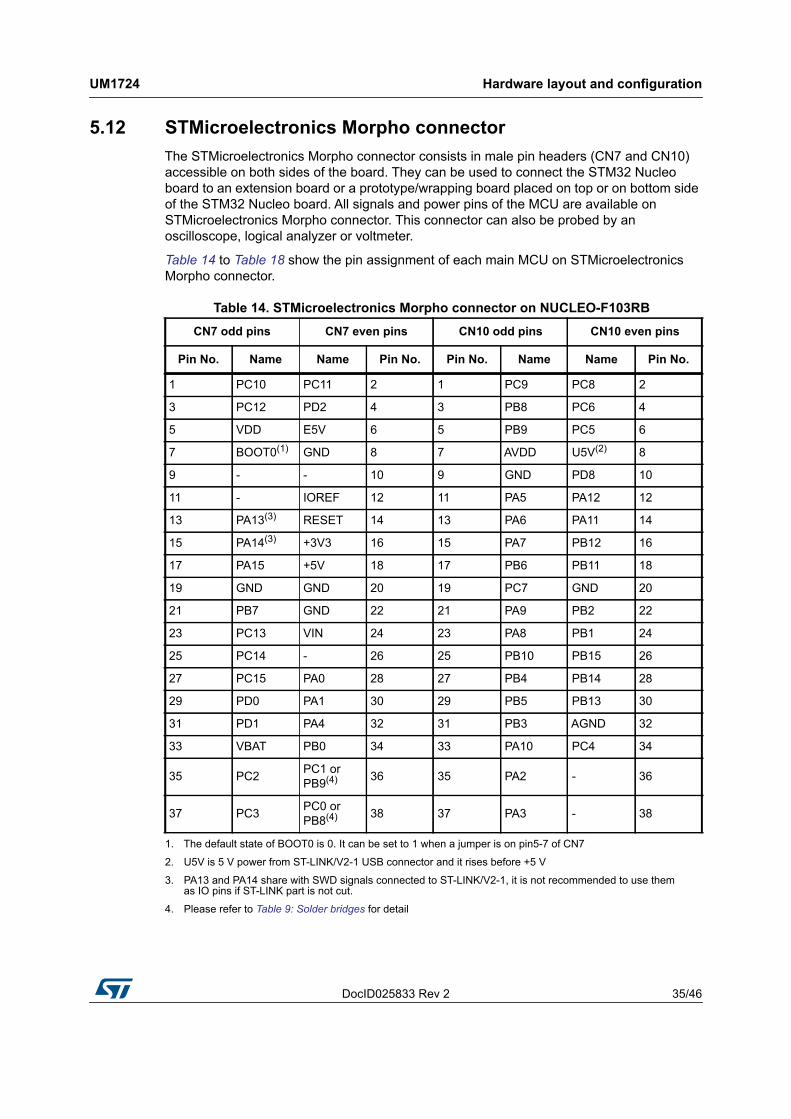
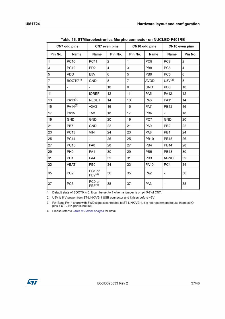
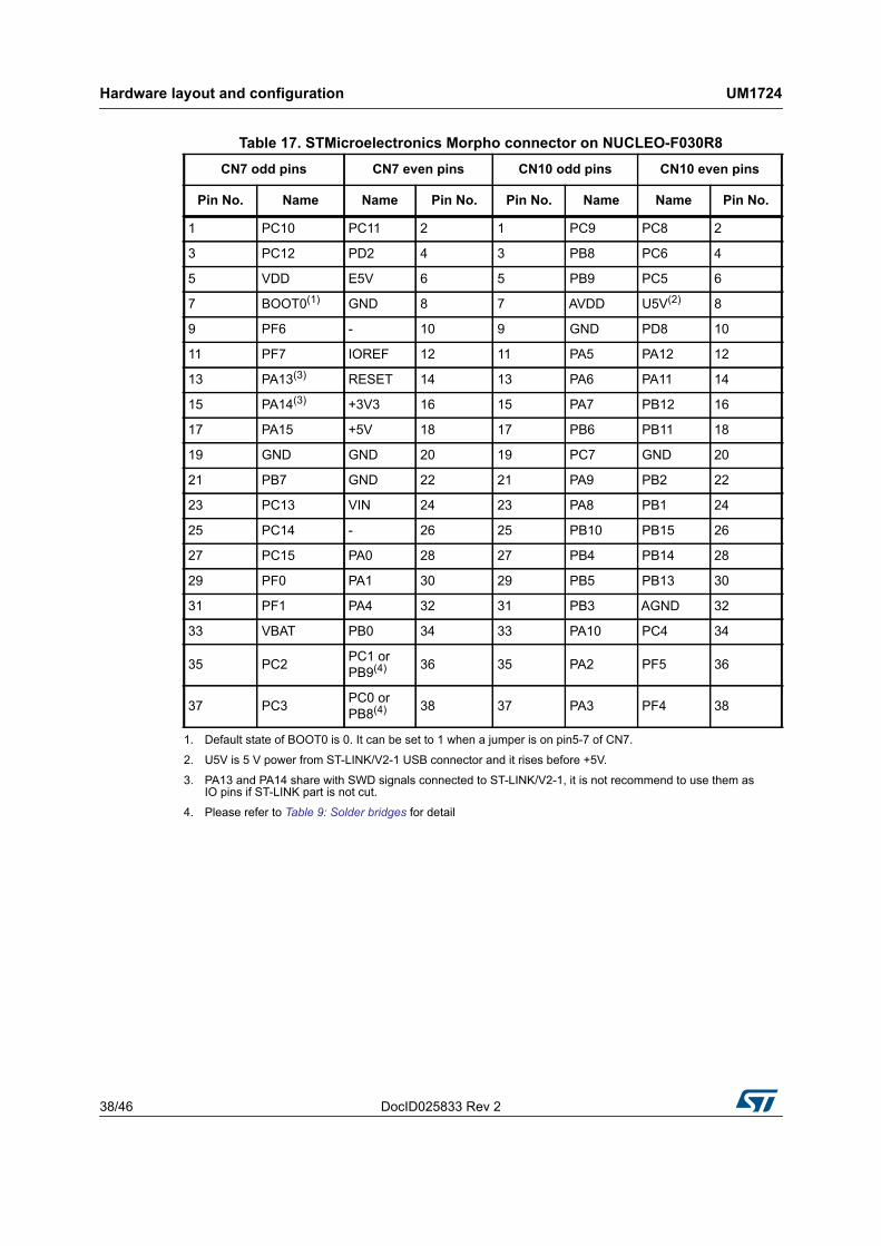
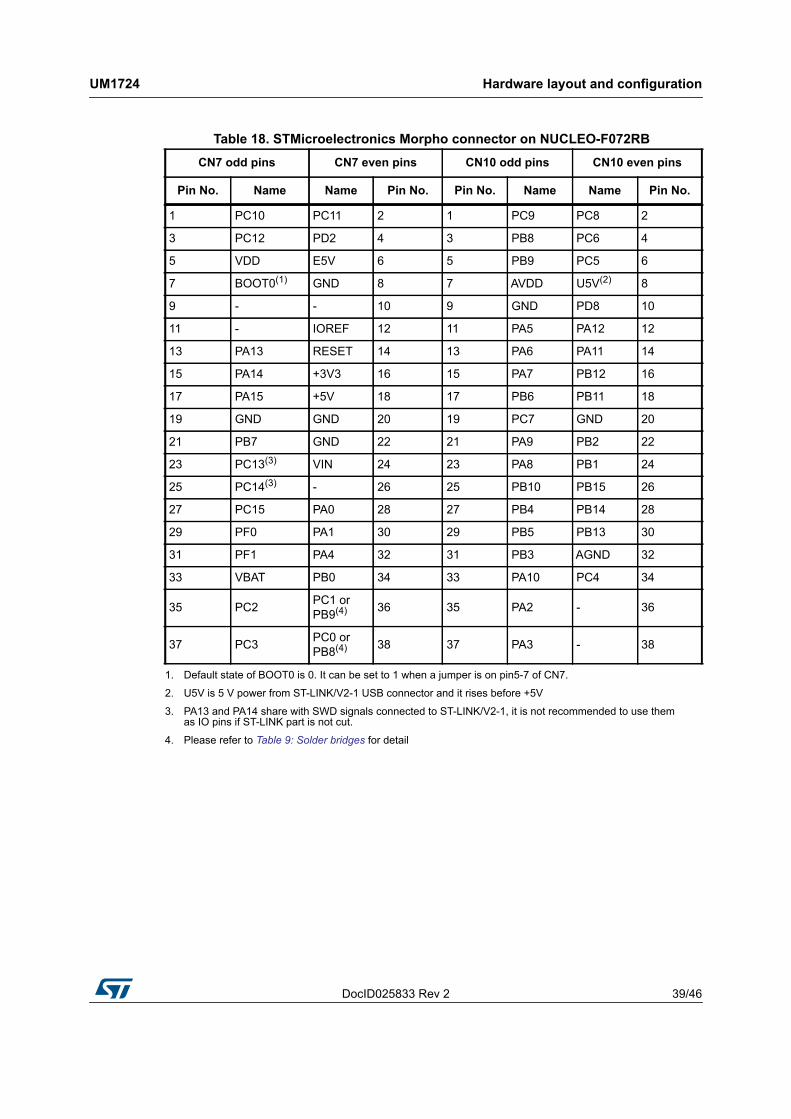
5.12 STMicroelectronics Morpho connector The STMicroelectronics Morpho connector consists in male pin headers (CN7 and CN10) accessible on both sides of the board. They can be used to connect the STM32 Nucleo board to an extension board or a prototype/wrapping board placed on top or on bottom side of the STM32 Nucleo board. All signals and power pins of the MCU are available on STMicroelectronics Morpho connector. This connector can also be probed by an oscilloscope, logical analyzer or voltmeter.
Table 14 to Table 18 show the pin assignment of each main MCU on STMicroelectronics Morpho connector.
Table 14. STMicroelectronics Morpho connector on NUCLEO-F103RB CN7 odd pins CN7 even pins CN10 odd pins CN10 even pins
Pin No. Name Name Pin No. Pin No. Name Name Pin No.
1 PC10 PC11 2 1 PC9 PC8 2
3 PC12 PD2 4 3 PB8 PC6 4
5 VDD E5V 6 5 PB9 PC5 6
7 BOOT0(1)
1. The default state of BOOT0 is 0. It can be set to 1 when a jumper is on pin5-7 of CN7
GND 8 7 AVDD U5V(2)
2. U5V is 5 V power from ST-LINK/V2-1 USB connector and it rises before +5 V
8
9 - - 10 9 GND PD8 10
11 - IOREF 12 11 PA5 PA12 12
13 PA13(3)
3. PA13 and PA14 share with SWD signals connected to ST-LINK/V2-1, it is not recommended to use them as IO pins if ST-LINK part is not cut.
RESET 14 13 PA6 PA11 14
15 PA14(3) +3V3 16 15 PA7 PB12 16
17 PA15 +5V 18 17 PB6 PB11 18
19 GND GND 20 19 PC7 GND 20
21 PB7 GND 22 21 PA9 PB2 22
23 PC13 VIN 24 23 PA8 PB1 24
25 PC14 - 26 25 PB10 PB15 26
27 PC15 PA0 28 27 PB4 PB14 28
29 PD0 PA1 30 29 PB5 PB13 30
31 PD1 PA4 32 31 PB3 AGND 32
33 VBAT PB0 34 33 PA10 PC4 34
35 PC2 PC1 or PB9(4)
4. Please refer to Table 9: Solder bridges for detail
36 35 PA2 - 36
37 PC3 PC0 or PB8(4) 38 37 PA3 - 38
Hardware layout and configuration UM1724
36/46 DocID025833 Rev 2
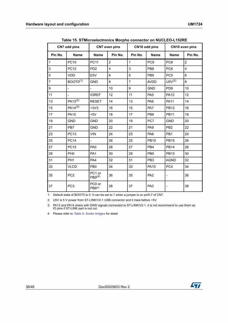
Table 15. STMicroelectronics Morpho connector on NUCLEO-L152RE CN7 odd pins CN7 even pins CN10 odd pins CN10 even pins
Pin No. Name Name Pin No. Pin No. Name Name Pin No.
1 PC10 PC11 2 1 PC9 PC8 2
3 PC12 PD2 4 3 PB8 PC6 4
5 VDD E5V 6 5 PB9 PC5 6
7 BOOT0(1)
1. Default state of BOOT0 is 0. It can be set to 1 when a jumper is on pin5-7 of CN7.
GND 8 7 AVDD U5V(2)
2. U5V is 5 V power from ST-LINK/V2-1 USB connector and it rises before +5V.
8
9 - - 10 9 GND PD8 10
11 - IOREF 12 11 PA5 PA12 12
13 PA13(3)
3. PA13 and PA14 share with SWD signals connected to ST-LINK/V2-1, it is not recommend to use them as IO pins if ST-LINK part is not cut.
RESET 14 13 PA6 PA11 14
15 PA14(3) +3V3 16 15 PA7 PB12 16
17 PA15 +5V 18 17 PB6 PB11 18
19 GND GND 20 19 PC7 GND 20
21 PB7 GND 22 21 PA9 PB2 22
23 PC13 VIN 24 23 PA8 PB1 24
25 PC14 - 26 25 PB10 PB15 26
27 PC15 PA0 28 27 PB4 PB14 28
29 PH0 PA1 30 29 PB5 PB13 30
31 PH1 PA4 32 31 PB3 AGND 32
33 VLCD PB0 34 33 PA10 PC4 34
35 PC2 PC1 or PB9(4)
4. Please refer to Table 9: Solder bridges for detail
36 35 PA2 - 36
37 PC3 PC0 or PB8(4) 38 37 PA3 - 38
DocID025833 Rev 2 37/46
UM1724 Hardware layout and configuration
45
Table 16. STMicroelectronics Morpho connector on NUCLEO-F401RE CN7 odd pins CN7 even pins CN10 odd pins CN10 even pins
Pin No. Name Name Pin No. Pin No. Name Name Pin No.
1 PC10 PC11 2 1 PC9 PC8 2
3 PC12 PD2 4 3 PB8 PC6 4
5 VDD E5V 6 5 PB9 PC5 6
7 BOOT0(1)
1. Default state of BOOT0 is 0. It can be set to 1 when a jumper is on pin5-7 of CN7.
GND 8 7 AVDD U5V(2)
2. U5V is 5 V power from ST-LINK/V2-1 USB connector and it rises before +5V
8
9 - - 10 9 GND PD8 10
11 - IOREF 12 11 PA5 PA12 12
13 PA13(3)
3. PA13and PA14 share with SWD signals connected to ST-LINK/V2-1, it is not recommend to use them as IO pins if ST-LINK part is not cut.
RESET 14 13 PA6 PA11 14
15 PA14(3) +3V3 16 15 PA7 PB12 16
17 PA15 +5V 18 17 PB6 - 18
19 GND GND 20 19 PC7 GND 20
21 PB7 GND 22 21 PA9 PB2 22
23 PC13 VIN 24 23 PA8 PB1 24
25 PC14 - 26 25 PB10 PB15 26
27 PC15 PA0 28 27 PB4 PB14 28
29 PH0 PA1 30 29 PB5 PB13 30
31 PH1 PA4 32 31 PB3 AGND 32
33 VBAT PB0 34 33 PA10 PC4 34
35 PC2 PC1 or PB9(4)
4. Please refer to Table 9: Solder bridges for detail
36 35 PA2 - 36
37 PC3 PC0 or PB8(4) 38 37 PA3 - 38
Hardware layout and configuration UM1724
38/46 DocID025833 Rev 2
Table 17. STMicroelectronics Morpho connector on NUCLEO-F030R8 CN7 odd pins CN7 even pins CN10 odd pins CN10 even pins
Pin No. Name Name Pin No. Pin No. Name Name Pin No.
1 PC10 PC11 2 1 PC9 PC8 2
3 PC12 PD2 4 3 PB8 PC6 4
5 VDD E5V 6 5 PB9 PC5 6
7 BOOT0(1)
1. Default state of BOOT0 is 0. It can be set to 1 when a jumper is on pin5-7 of CN7.
GND 8 7 AVDD U5V(2)
2. U5V is 5 V power from ST-LINK/V2-1 USB connector and it rises before +5V.
8
9 PF6 - 10 9 GND PD8 10
11 PF7 IOREF 12 11 PA5 PA12 12
13 PA13(3)
3. PA13 and PA14 share with SWD signals connected to ST-LINK/V2-1, it is not recommend to use them as IO pins if ST-LINK part is not cut.
RESET 14 13 PA6 PA11 14
15 PA14(3) +3V3 16 15 PA7 PB12 16
17 PA15 +5V 18 17 PB6 PB11 18
19 GND GND 20 19 PC7 GND 20
21 PB7 GND 22 21 PA9 PB2 22
23 PC13 VIN 24 23 PA8 PB1 24
25 PC14 - 26 25 PB10 PB15 26
27 PC15 PA0 28 27 PB4 PB14 28
29 PF0 PA1 30 29 PB5 PB13 30
31 PF1 PA4 32 31 PB3 AGND 32
33 VBAT PB0 34 33 PA10 PC4 34
35 PC2 PC1 or PB9(4)
4. Please refer to Table 9: Solder bridges for detail
36 35 PA2 PF5 36
37 PC3 PC0 or PB8(4) 38 37 PA3 PF4 38
DocID025833 Rev 2 39/46
UM1724 Hardware layout and configuration
45
Table 18. STMicroelectronics Morpho connector on NUCLEO-F072RB CN7 odd pins CN7 even pins CN10 odd pins CN10 even pins
Pin No. Name Name Pin No. Pin No. Name Name Pin No.
1 PC10 PC11 2 1 PC9 PC8 2
3 PC12 PD2 4 3 PB8 PC6 4
5 VDD E5V 6 5 PB9 PC5 6
7 BOOT0(1)
1. Default state of BOOT0 is 0. It can be set to 1 when a jumper is on pin5-7 of CN7.
GND 8 7 AVDD U5V(2)
2. U5V is 5 V power from ST-LINK/V2-1 USB connector and it rises before +5V
8
9 - - 10 9 GND PD8 10
11 - IOREF 12 11 PA5 PA12 12
13 PA13 RESET 14 13 PA6 PA11 14
15 PA14 +3V3 16 15 PA7 PB12 16
17 PA15 +5V 18 17 PB6 PB11 18
19 GND GND 20 19 PC7 GND 20
21 PB7 GND 22 21 PA9 PB2 22
23 PC13(3)
3. PA13 and PA14 share with SWD signals connected to ST-LINK/V2-1, it is not recommended to use them as IO pins if ST-LINK part is not cut.
VIN 24 23 PA8 PB1 24
25 PC14(3) - 26 25 PB10 PB15 26
27 PC15 PA0 28 27 PB4 PB14 28
29 PF0 PA1 30 29 PB5 PB13 30
31 PF1 PA4 32 31 PB3 AGND 32
33 VBAT PB0 34 33 PA10 PC4 34
35 PC2 PC1 or PB9(4)
4. Please refer to Table 9: Solder bridges for detail
36 35 PA2 - 36
37 PC3 PC0 or PB8(4) 38 37 PA3 - 38
Mechanical drawing UM1724
40/46 DocID025833 Rev 2
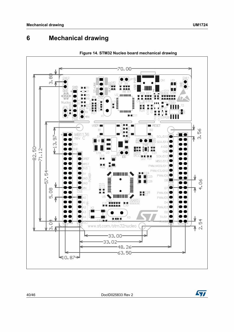
6 Mechanical drawing
Figure 14. STM32 Nucleo board mechanical drawing
DocID025833 Rev 2 41/46
UM1724 Electrical schematics
45
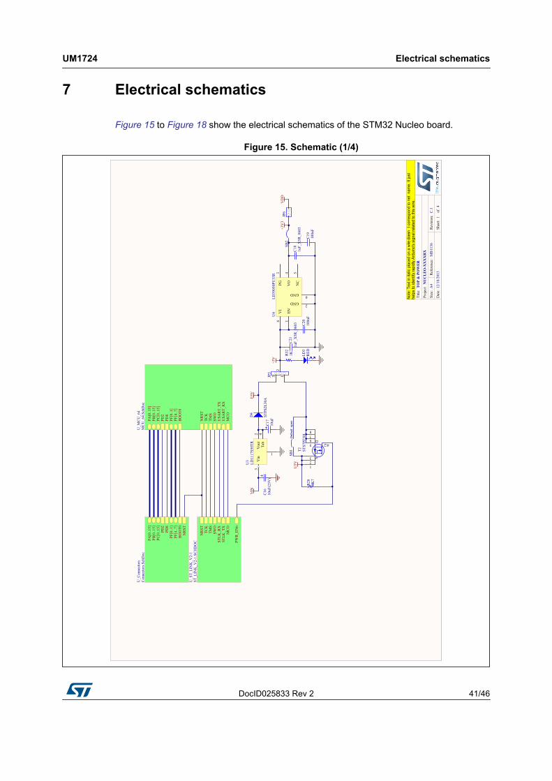
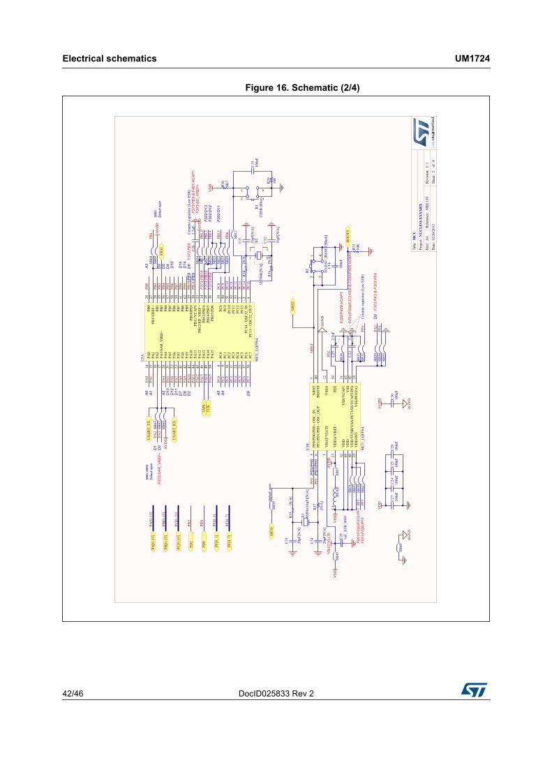
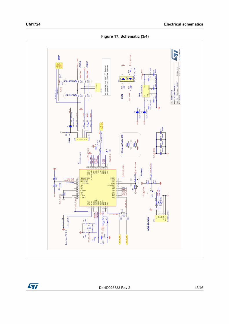
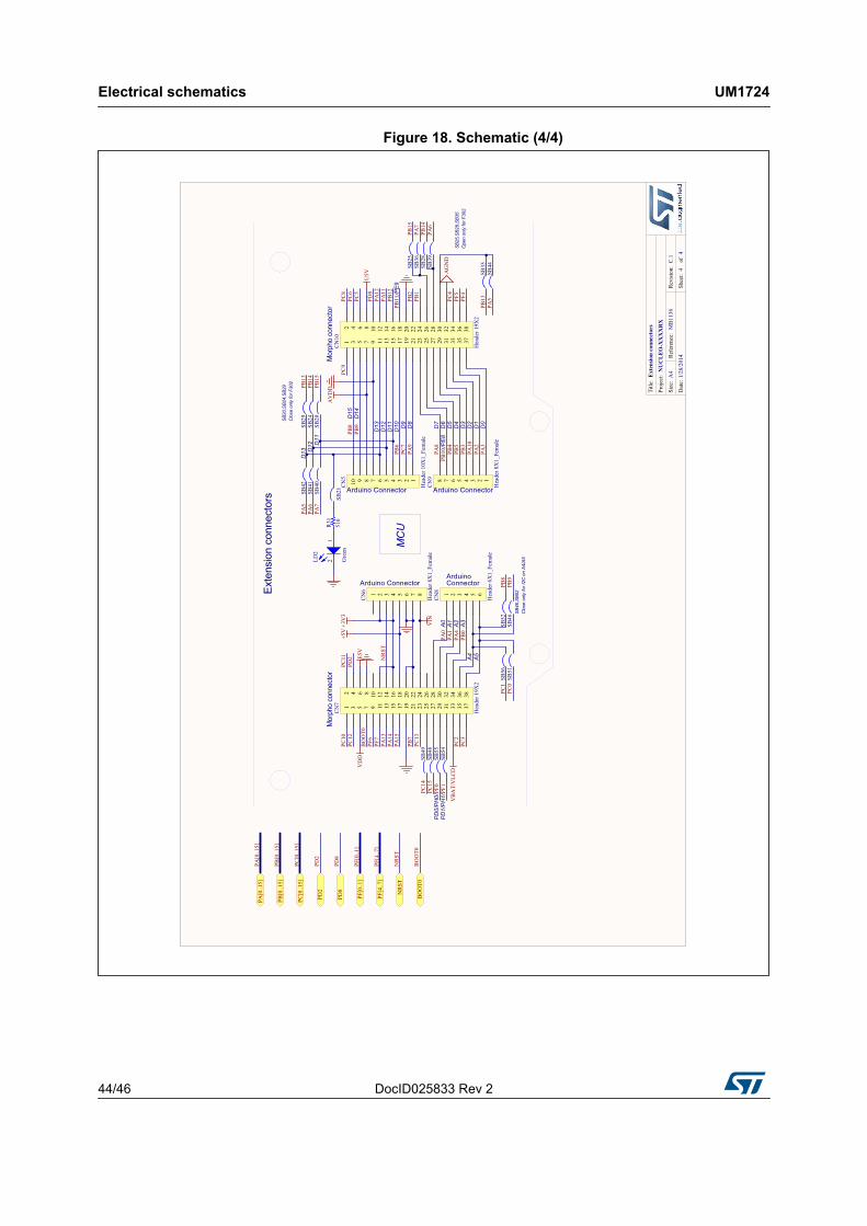
7 Electrical schematics
Figure 15 to Figure 18 show the electrical schematics of the STM32 Nucleo board.
Figure 15. Schematic (1/4)
14
TOP & POWER
MB11
36C.1
12/18/2013
Title:
Size:
Reference:
Date:
Sheet:
of
A4
Revision:
NUCLEO
-XXXXRX
Project:
R28
4K7
U5V
+3V3
C18
1uF_
X5R
_060
3C20
100nF
C19
100nF
VIN
+5V
VDD
JP6
TMS
TCK
MCO
NRST
STLK
_RX
STLK
_TX
SWO
PWR_E
Nn
U_S
T_LINK_V
2-1
ST_L
INK_V
2-1.SC
HDOC
LD3
REDR32
1K
4
3
5 G
SD6
78
21
T2 STS7
PF30L
C16
10uF
(25V
)C17
10uF
Vin
3Vou
t2
1
Tab
4
U3
LD11
17S5
0TR
PA[0..1
5]PB
[0..15]
PC[0..15]
PF[4..7
]
PD2
PD8
PF[0..1
]
NRST
BOOT0
U_C
onnectors
Connectors.S
chDoc
NRST
MCO
USA
RT_
RX
USA
RT_
TX
PA[0..1
5]PB
[0..15]
PC[0..15]
PF[4..7
]
PD2
TCK
TMS
SWO
PD8
PF[0..1
]
BOOT0
U_M
CU_6
4MCU_6
4.SchD
oc
SB1
SB2
EN1
GND 2
VO
4
NC
5
GND 0
VI
6PG
3U4
LD39
050P
U33R
Note: Tex
t in ita
lic place
d on
a wire doe
snt c
orresp
ond to net n
ame. It ju
st
helps to id
entify rapidly Ardu
ino's sign
al re
lated to th
is wire
.
Defau
lt: ope
n
32
1JP5
C21
1uF_
X5R
_060
3
E5V
D4
STPS
2L30A
Electrical schematics UM1724
42/46 DocID025833 Rev 2
Figure 16. Schematic (2/4)
24
MCU
MB11
36C.1
12/20/2013
Title:
Size:
Reference:
Date:
Sheet:
of
A4
Revision:
NUCLEO
-XXXXRX
Project:
C23
100nF
C28
100nF
C24
100nF
C34
20pF
[N/A]
C33
20pF
[N/A]
X3
8MHz(16
pF)[N/A]
R37
[N/A] C27
100nF
PC13
2
PC14
- OSC
32_IN
3
PC15
- OSC
32_O
UT
4
PC0
8
PC1
9
PC2
10
PC3
11
PA0
14
PA1
15
PA2
16
PA3/SA
R_V
REF
+17
PA4
20
PA5
21
PA6
22
PA7
23
PC4
24
PC5
25
PB0
26
PB1/VREF
+27
PB2
28
PB10/PE8
29
PB11/VCAP1
30
PB12
/SD_V
REF
+33
PB13
/PB14
34
PB14
/PB15
35
PB15
/PD8
36
PC6
37
PC7
38
PC8
39
PC9
40
PA8
41
PA9
42
PA10
43
PA11
44
PA12
45
PA13
46
PA14
49
PA15
50
PC10
51
PC11
52
PC12
53
PB3
55
PB4
56
PB5
57
PB6
58
PB7
59
PB8
61
PB9
62
U5A
MCU_L
QFP
64
VBAT/VLC
D1
PF0/PD
0/PH
0 - O
SC_IN
5
PF1/PD
1/PH
1 - O
SC_O
UT
6NRST
7
VSS
A12
VDDA/V
REF
+13
VSS
/PF4
/PA3
18VDD/PF5
19
VSS
/VCAP1
31VDD
32
VSS
/VCAP2
/PF6
47VDD/V
USB
/VSA
/PF7
48
BOOT0
60
VSS
63VDD
64
PD2
54
U5B
MCU_L
QFP
64
41
32
X2
32.768K[N
/A]
C32
10pF
[N/A]
C31
10pF
[N/A]
R36
[N/A]
R34
[N/A] 1 4
32B2
TD-034
1 [R
ESET
/Black]
C14
100nF
R33
10K
R30
4K7
1
43
2
B1
USE
R (B
lue)
C15
100nF
R29
100
PA4
PA5
PA6
PA7
PA11
PA12
PA9
PA10
PA0
PA1
PA15
PA3
PA13
PA14
PA2
PA8
NRST
PB5
PB6
PB7
PB14
PB15
PB10
PB8
PB9
PB1
PB2
PB3
PB0
PB4
PB11
PB12
PB13
PC0
PC1
PC2
PC3
PC4
PC5
PC6
PC7
PC8
PC9
PC10
PC11
PC12
PC13
PC14
PC15
A0
A1
A2
A3
A4
A5
D0
D1
D12
D11
D13
D14
D15
PA3
D0
PD8
PF4
PF6
PF7
PF5
NRST
MCO
USA
RT_
RX
USA
RT_
TX
VDD
VDD
VDD
L1BEA
D
AVDD
SB17
PA[0..1
5]PA
[0..1
5]
PB[0..15]
PB[0..15]
PC[0..15]
PC[0..15]
PF[4..7
]PF
[4..7
]
PD2
PD2
TCK
TMS
SWO
AVDD
/PE9
/PE8
AVDD
PD2
PD8
PD8
PF0
PF1
/PD0/PH0
/PD1/PH1
PF[0..1
]PF
[0..1
]
F373
:SAR_V
REF+
F373
:PA3 & F3
03:PF4
F051
/F03
0:PF5
F373
:PE8
F373
:PE9 & F4
01:VCAP1
F200
/F42
9:VCAP1
F373
:SD_V
REF+
F373
:PB14
F373
:PB15
F373
:PD8
F051
/F03
0/F3
73:PF6
& F20
0/F4
29:VCAP2
F051
/F03
0/F3
73:PF7
AGND
AVDD C30
100nF
AGND
R35
[N/A]
C29
1uF_
X5R
_060
3
SB45
VDD
VBAT/VLC
D
Ceram
ic capacito
r (Lo
w ESR
)
Ceram
ic capacito
r (Lo
w ESR
)
BOOT0
C26
2.2u
F
C25
2.2u
F
C22
2.2u
F
SB60
AGND
SB63
SB62
SB61
SB34
SB27
SB26
SB23
SB22
SB19
SB18
SB31
SB43
SB30
SB47
SB38
SB33
SB32
SB59
SB58
SB53
SB57
SB37
SB50
Defau
lt: ope
n
F302
:D12
F302
:D11
F302
:D13
D2
D4
D3
D5
D6
D7
D8
D9
D10SB
64SB
65AVDD
Defau
lt op
enSB
62,SB6
3
Defau
lt op
enSB
65
DocID025833 Rev 2 43/46
UM1724 Electrical schematics
45
Figure 17. Schematic (3/4)
34
STLIN
K/V2-1
MB11
36C.1
1/28/2014
Title:
Size:
Reference:
Date:
Sheet:
of
A4
Revision:
NUCLEO
-XXXXRX
Project:
12
X1
8MHz(12
pF)
USB
_DM
USB
_DP
STM_R
ST
T_JTCK
T_JT
CK
T_JTDOT_JTDI
T_JT
MS
STM_J
TMS
STM_JTCK
OSC
_IN
OSC
_OUT
T_NRST
AIN_1
USB
ST-LINK
U5V
COM PWR
Jumper
s ON --> N
UCLE
O S
elec
ted
Jumper
s OFF
-->
ST-L
INK S
elec
ted
Board Iden
t: PC
13=0
T_JT
CK
T_JT
MS
SWD
1234
CN2
SB3
SB4
SB5
SB6
SB7
SB8
SB9
SB10
STM_J
TMS
STM_J
TCK
SWCL
K
SWDIO
SWD
RESERVED
DEFAULT
T_SW
DIO
_IN
LED_S
TLINK
LED_S
TLINK
TMS
TCK
TCK/SWCLK
TMS/SW
DIO
MCO
MCO
T_JRST
AIN_1
T_NRST
T_SW
O
NRST
SB12
T_NRST
SB11
D1
BAT6
0JFILM
CN3
TX RX
STLINK_R
X
Not Fitted
SB14
SB13
STLK
_RX
STLK
_TX
STLINK_TX
USB
_DM
USB
_DP
VCC
1
D-
2
D+
3
ID4
GND
5
SHEL
L6
CN1
5075
BMR-05-SM
T_SW
O
SWO
SB15
T_SW
O
Red
_Green
21
34
LD1
LD_B
ICOLO
R_C
MS
R16
1K5
R18
0R17
0R15
100K
R21
100
R20
100
R19
0
R9
100[N/A]
R5
22
R8
22
R13
22
R22
22
R25
100
R24
100
R1
10K
R2
10K[N
/A]
R14
100K
R6
100K
R3
10K
R23
4K7
R27
4K7
C11
100nF
C4
100nF
C1
100nF
C7
100nF
C10
20pF
[N/A]
C3
20pF
C8
20pF
C6
100nF
1 2 3 4 5 6
CN4
Header 6
X1
U5V
USB
_REN
UMn
USB_RENUMn
PWR_E
Nn
R7
2K7
R4
4K7
+3V3_
ST_L
INK
+3V3_
ST_L
INK
+3V3_
ST_L
INK
+3V3_
ST_L
INK
+3V3_
ST_L
INK
+3V3_
ST_L
INK
+3V3_
ST_L
INK
JP1
+3V3_
ST_L
INK
PWR_EXT
+3V3_
ST_L
INK
+3V3
SB16
Defau
lt: ope
n
D2
BAT6
0JFILM
D3
BAT6
0JFILM
C2
1uF_
X5R
_060
3
C9
10nF
_X7R
_060
3
C13
1uF_
X5R
_060
3
51
2
GND
3
4
BYPA
SSIN
H
Vin
Vou
t
U1
LD39
85M33
R
C5
100nF
C12
100nF
+3V3_
ST_L
INK
3
2
1
T1 9013
R12
10K
R10
36K
U5V
R11
100
+3V3_
ST_L
INK
CN11
Wire
d on
Solder S
ide
CN12
E5V
E5V
+3V3_
ST_L
INK
JP4
R26
[N/A]
VBAT
1
PA7 17
PC13
2
PA12
33PC
143
PB0 18
PC15
4JT
MS/SW
DIO
34
OSC
IN5
PB1 19
OSC
OUT
6
VSS
_235
NRST
7
PB2/BOOT1 20
VSS
A8
VDD_2
36
VDDA
9
PB10 21
PA0
10
JTCK/SWCLK37
PA1
11
PB11 22
PA2
12
PA15/JTDI38
PA3 13
VSS_1 23
PA4 14
PB3/JTDO39
PA5 15
VDD_1 24
PA6 16
PB4/JNTRST40
PB12
25
PB541
PB13
26
PB642
PB14
27
PB743
PB15
28
BOOT044
PA8
29
PB845
PA9
30
PB946
PA10
31
VSS_347
PA11
32
VDD_348
U2
STM32F1
03CBT6
Electrical schematics UM1724
44/46 DocID025833 Rev 2
Figure 18. Schematic (4/4)
44
Extension conn
ectors MB11
36C.1
1/28/2014
Title:
Size:
Reference:
Date:
Sheet:
of
A4
Revision:
NUCLEO
-XXXXRX
Project:
Extens
ion co
nnec
tors
+3V3
+5V
A0
A1
A2
A3
A4
A5
D0
D1
D2
D4
D3
D5
D6
D7
D8
D9
D10
D12 D
11
D13
D14
D15
PA0
PA2
PA4
PA5
PA6
PA7
PA10
PA3
PB0
PB1
PB3
PB4
PB8
PB9
PA11
PA12
PA9
PA1
PA15
PA13
PA14
PA8
PC0
PC1
PC2
PC3
PC4
PC5
PC6
PC7
PB5
PB6
PB7
PB14
PB15
PB2
PB11PB
12
PB13PC
8PC
9PC
10PC
11PC
12
PC13
PC14
PC15
PB10
PD8
PF4
PF6
PF7
1 2 3 4 5 6
CN8
Header 6
X1_Female
1 2 3 4 5 6 7 8
CN6
Header 8
X1_Female
12345678
CN9
Header 8
X1_Female
12345678910CN5
Header 1
0X1_Female
NRST
VIN
/PE9
/PE8
PD2
PF0
PF1
PA[0..1
5]PA
[0..1
5]
PB[0..15]
PB[0..15]
PC[0..15]
PC[0..15]
PD2
PD2
PD8
PD8
PF[0..1
]PF
[0..1
]
AGND
NRST
NRST
SB48
SB49
SB55
SB54
AVDD
U5V
VDD
BOOT0
BOOT0
BOOT0
VBAT/VLC
D
PF[4..7
]PF
[4..7
]
PF5
SB56
SB51
SB52
SB46
PB8
PB9
SB29
SB42
SB41
SB24
SB40
SB20
D13
D12
D11
PB13
PB15
PB14
SB25
SB36
SB28
SB39
SB35
SB44
PA5
PA6
PA7
MCU
Close
only for I2C
on A4
/A5
SB46
,SB5
2
Arduino Connector Arduino Connector
Arduino Connector
12
34
56
78
910
1112
1314
1516
1718
1920
2122
2324
2526
2728
2930
3132
3334
3536
3738
CN7
Header 1
9X2
12
34
56
78
910
1112
1314
1516
1718
1920
2122
2324
2526
2728
2930
3132
3334
3536
3738
CN10
Header 1
9X2
ArduinoConnector
12LD
2
Green
R31
510
SB21
E5V
PD0/PH0/
PD1/PH1/
Close
only for F
302
SB20
,SB2
4,SB
29
Ope
n on
ly fo
r F30
2SB
25,SB2
8,SB
35
Morph
o co
nnec
tor
Morph
o co
nnec
tor
DocID025833 Rev 2 45/46
UM1724 References
45
8 References
9 Revision history
1. UM1075 - ST-LINK/V2 in-circuit debugger/programmer for STM8 and STM32, User manual
Table 19. Document revision historyDate Revision Changes
10-Feb-2014 1 Initial release.
13-Feb-2014 2 Updated Figure 1, Chapter 4 and Table 9.
UM1724
46/46 DocID025833 Rev 2
Please Read Carefully:
Information in this document is provided solely in connection with ST products. STMicroelectronics NV and its subsidiaries (“ST”) reserve the right to make changes, corrections, modifications or improvements, to this document, and the products and services described herein at any time, without notice.
All ST products are sold pursuant to ST’s terms and conditions of sale.
Purchasers are solely responsible for the choice, selection and use of the ST products and services described herein, and ST assumes no liability whatsoever relating to the choice, selection or use of the ST products and services described herein.
No license, express or implied, by estoppel or otherwise, to any intellectual property rights is granted under this document. If any part of this document refers to any third party products or services it shall not be deemed a license grant by ST for the use of such third party products or services, or any intellectual property contained therein or considered as a warranty covering the use in any manner whatsoever of such third party products or services or any intellectual property contained therein.
UNLESS OTHERWISE SET FORTH IN ST’S TERMS AND CONDITIONS OF SALE ST DISCLAIMS ANY EXPRESS OR IMPLIED WARRANTY WITH RESPECT TO THE USE AND/OR SALE OF ST PRODUCTS INCLUDING WITHOUT LIMITATION IMPLIED WARRANTIES OF MERCHANTABILITY, FITNESS FOR A PARTICULAR PURPOSE (AND THEIR EQUIVALENTS UNDER THE LAWS OF ANY JURISDICTION), OR INFRINGEMENT OF ANY PATENT, COPYRIGHT OR OTHER INTELLECTUAL PROPERTY RIGHT.
ST PRODUCTS ARE NOT DESIGNED OR AUTHORIZED FOR USE IN: (A) SAFETY CRITICAL APPLICATIONS SUCH AS LIFE SUPPORTING, ACTIVE IMPLANTED DEVICES OR SYSTEMS WITH PRODUCT FUNCTIONAL SAFETY REQUIREMENTS; (B) AERONAUTIC APPLICATIONS; (C) AUTOMOTIVE APPLICATIONS OR ENVIRONMENTS, AND/OR (D) AEROSPACE APPLICATIONS OR ENVIRONMENTS. WHERE ST PRODUCTS ARE NOT DESIGNED FOR SUCH USE, THE PURCHASER SHALL USE PRODUCTS AT PURCHASER’S SOLE RISK, EVEN IF ST HAS BEEN INFORMED IN WRITING OF SUCH USAGE, UNLESS A PRODUCT IS EXPRESSLY DESIGNATED BY ST AS BEING INTENDED FOR “AUTOMOTIVE, AUTOMOTIVE SAFETY OR MEDICAL” INDUSTRY DOMAINS ACCORDING TO ST PRODUCT DESIGN SPECIFICATIONS. PRODUCTS FORMALLY ESCC, QML OR JAN QUALIFIED ARE DEEMED SUITABLE FOR USE IN AEROSPACE BY THE CORRESPONDING GOVERNMENTAL AGENCY.
Resale of ST products with provisions different from the statements and/or technical features set forth in this document shall immediately void any warranty granted by ST for the ST product or service described herein and shall not create or extend in any manner whatsoever, any liability of ST.
ST and the ST logo are trademarks or registered trademarks of ST in various countries.Information in this document supersedes and replaces all information previously supplied.
The ST logo is a registered trademark of STMicroelectronics. All other names are the property of their respective owners.
© 2014 STMicroelectronics - All rights reserved
STMicroelectronics group of companies
Australia - Belgium - Brazil - Canada - China - Czech Republic - Finland - France - Germany - Hong Kong - India - Israel - Italy - Japan - Malaysia - Malta - Morocco - Philippines - Singapore - Spain - Sweden - Switzerland - United Kingdom - United States of America
www.st.com