ssf 14230 road vehicles - diagnostic systemsread.pudn.com/downloads122/ebook/519812/ssf 14230-1t...
TRANSCRIPT

SSF 14230 Road Vehicles - Diagnostic Systems
Keyword Protocol 2000 - Part 1 - Physical LayerTest Specification
Swedish Recommended Practice
Document: SSF 14230-T1
Status: Issue 1
Date: April 1, 1998
This document is based on the InternationalStandards ISO 9141-3 and ISO 14230-1and hasbeen further developed to meet Swedishautomotive manufacturer's requirements by theSwedish Vehicle Diagnostics Task Force.It is based on mutual agreement between thefollowing companies:
•••• Saab Automobile AB•••• SCANIA AB•••• Volvo Car Corp.•••• Volvo Bus Corp.•••• Mecel AB
File: 14230-T1.doc / Definition by “Samarbetsgruppen för Svensk Fordonsdiagnos” / Author: L. Magnusson Mecel AB
http://www.mecel.se/html/ssf.htm
KWP 2000 - Part 1 - Physical Layer Test Specification, Swedish Recommended Practice
SSF 14230-T1 Issue 12 of 37
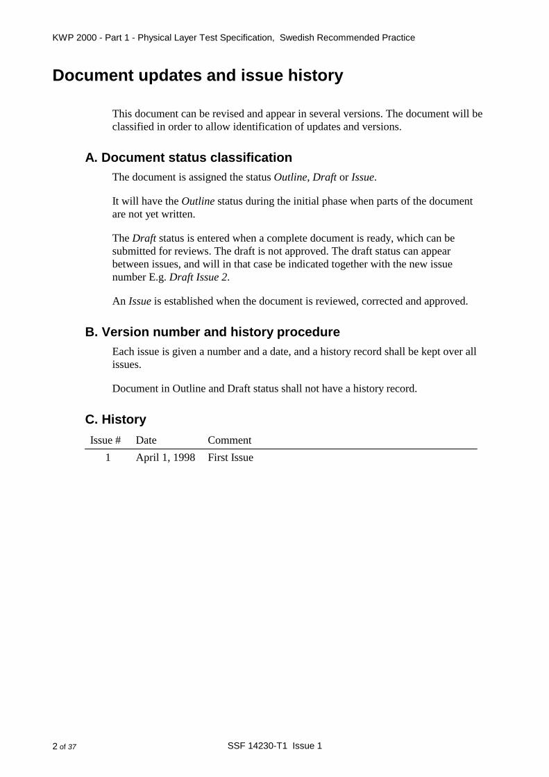
Document updates and issue history
This document can be revised and appear in several versions. The document will beclassified in order to allow identification of updates and versions.
A. Document status classification
The document is assigned the status Outline, Draft or Issue.
It will have the Outline status during the initial phase when parts of the documentare not yet written.
The Draft status is entered when a complete document is ready, which can besubmitted for reviews. The draft is not approved. The draft status can appearbetween issues, and will in that case be indicated together with the new issuenumber E.g. Draft Issue 2.
An Issue is established when the document is reviewed, corrected and approved.
B. Version number and history procedure
Each issue is given a number and a date, and a history record shall be kept over allissues.
Document in Outline and Draft status shall not have a history record.
C. History
Issue # Date Comment
1 April 1, 1998 First Issue

KWP 2000 - Part 1 - Physical Layer Test Specification, Swedish Recommended Practice
SSF 14230-T1 Issue 1 3 of 37
Table of contents
1 REFERENCES .........................................................................................................................................................4
2 DEFINITIONS AND ABBREVIATIONS..............................................................................................................5
3 GENERAL ................................................................................................................................................................6
3.1 REQUIREMENTS CROSS REFERENCE LIST..............................................................................................................6
4 ECU TESTS ..............................................................................................................................................................7
4.1 ELECTRICAL SPECIFICATION.................................................................................................................................7
4.1.1 Resistance test.............................................................................................................................................7
4.1.2 Capacitance test..........................................................................................................................................8
4.1.3 Over voltages and transients ......................................................................................................................9
4.2 SIGNAL LEVEL TESTS .........................................................................................................................................10
4.2.1 Transmission state ....................................................................................................................................10
4.2.2 Receiving state ..........................................................................................................................................13
4.2.3 Bit shift......................................................................................................................................................14
5 TEST TOOL TESTS ..............................................................................................................................................15
5.1 ELECTRICAL SPECIFICATION...............................................................................................................................15
5.1.1 Resistance test...........................................................................................................................................15
5.1.2 Capacitance test........................................................................................................................................16
5.1.3 Voltage transients .....................................................................................................................................17
5.2 SIGNAL LEVEL TESTS .........................................................................................................................................18
5.2.1 Transmission state ....................................................................................................................................18
5.2.2 Receiving state ..........................................................................................................................................19
5.2.3 Bit shift......................................................................................................................................................21
6 APPENDIX .............................................................................................................................................................23

KWP 2000 - Part 1 - Physical Layer Test Specification, Swedish Recommended Practice
SSF 14230-T1 Issue 14 of 37
1 References
1. SSF 14230-1 Road vehicles-Diagnostic systemsKeyword protocol 2000-Part 1-Physical layer, Swedish Implementation Standard
2. SSF 14230-2 Road vehicles-Diagnostic systemsKeyword protocol 2000-Part 2-Data Link layer, Swedish Implementation Standard
3. [ECU specification]
4. [Test Tool specification]
KWP 2000 - Part 1 - Physical Layer Test Specification, Swedish Recommended Practice
SSF 14230-T1 Issue 1 5 of 37
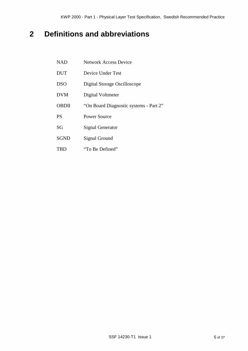
2 Definitions and abbreviations
NAD Network Access Device
DUT Device Under Test
DSO Digital Storage Oscilloscope
DVM Digital Voltmeter
OBDII “On Board Diagnostic systems - Part 2”
PS Power Source
SG Signal Generator
SGND Signal Ground
TBD “To Be Defined”
KWP 2000 - Part 1 - Physical Layer Test Specification, Swedish Recommended Practice
SSF 14230-T1 Issue 16 of 37
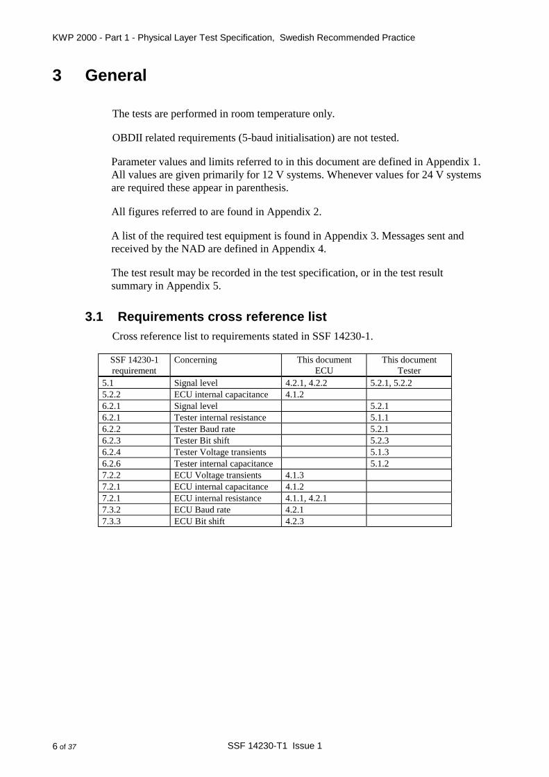
3 General
The tests are performed in room temperature only.
OBDII related requirements (5-baud initialisation) are not tested.
Parameter values and limits referred to in this document are defined in Appendix 1.All values are given primarily for 12 V systems. Whenever values for 24 V systemsare required these appear in parenthesis.
All figures referred to are found in Appendix 2.
A list of the required test equipment is found in Appendix 3. Messages sent andreceived by the NAD are defined in Appendix 4.
The test result may be recorded in the test specification, or in the test resultsummary in Appendix 5.
3.1 Requirements cross reference list
Cross reference list to requirements stated in SSF 14230-1.
SSF 14230-1requirement
Concerning This documentECU
This documentTester
5.1 Signal level 4.2.1, 4.2.2 5.2.1, 5.2.25.2.2 ECU internal capacitance 4.1.26.2.1 Signal level 5.2.16.2.1 Tester internal resistance 5.1.16.2.2 Tester Baud rate 5.2.16.2.3 Tester Bit shift 5.2.36.2.4 Tester Voltage transients 5.1.36.2.6 Tester internal capacitance 5.1.27.2.2 ECU Voltage transients 4.1.37.2.1 ECU internal capacitance 4.1.27.2.1 ECU internal resistance 4.1.1, 4.2.17.3.2 ECU Baud rate 4.2.17.3.3 ECU Bit shift 4.2.3
KWP 2000 - Part 1 - Physical Layer Test Specification, Swedish Recommended Practice
SSF 14230-T1 Issue 1 7 of 37
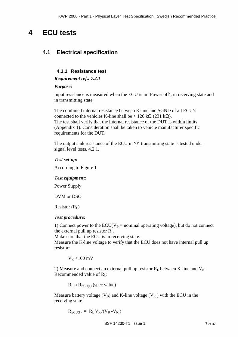
4 ECU tests
4.1 Electrical specification
4.1.1 Resistance test
Requirement ref.: 7.2.1
Purpose:
Input resistance is measured when the ECU is in ‘Power off‘, in receiving state andin transmitting state.
The combined internal resistance between K-line and SGND of all ECU’sconnected to the vehicles K-line shall be > 126 kΩ (231 kΩ).The test shall verify that the internal resistance of the DUT is within limits(Appendix 1). Consideration shall be taken to vehicle manufacturer specificrequirements for the DUT.
The output sink resistance of the ECU in ‘0’-transmitting state is tested undersignal level tests, 4.2.1.
Test set-up:
According to Figure 1
Test equipment:
Power Supply
DVM or DSO
Resistor (RL)
Test procedure:
1) Connect power to the ECU(VB = nominal operating voltage), but do not connectthe external pull up resistor RL.Make sure that the ECU is in receiving state.Measure the K-line voltage to verify that the ECU does not have internal pull upresistor:
VK <100 mV
2) Measure and connect an external pull up resistor RL between K-line and VB.Recommended value of RL:
RL ≈ RECU(1) (spec value)
Measure battery voltage (VB) and K-line voltage (VK ) with the ECU in thereceiving state.
RECU(1) = RL VK /(VB -VK )

KWP 2000 - Part 1 - Physical Layer Test Specification, Swedish Recommended Practice
SSF 14230-T1 Issue 18 of 37
3) Disconnect battery voltage (VB) from the ECU.
Measure battery voltage (VB) and K-line voltage (VK ) with the ECU in “PowerOff” state.
RECU(1) = RL VK /(VB -VK )
Test result:
Test case Measured values Calc.VB VK RL Ω RECU(1) Ω OK
1) Int. pull up2) Receiving3) Power off
4.1.2 Capacitance test
Requirement ref.: 7.2.1, 5.2.2
Purpose:
The test shall verify that the capacitance of the ECU does not exceed CECUi.Consideration shall be taken to vehicle manufacturer specific requirements for theDUT.
Test set-up:
According to Figure 2.
Use short leads to reduce stray capacitance which will add to the measuredcapacitance.
Test equipment:
Power Supply
DSO
Signal Generator, diode, resistor (R = 1 kΩ)
Test procedure:
Connect signal generator (SG), diode (D), resistor (R) and DSO according toFigure 2.Connect power to the ECU(VB = nominal operating voltage)Set up the signal generator to produce a square wave signal. Recommendedfrequency = 1 kHz and output voltage Vmax = 12 V (24 V)Make sure that the ECU is in receiving state.
Measure fall time and calculate the capacitance (if necessary adjust the signalfrequency). Use the measured value (test 4.1.1) of RECU(1) in the calculation.

KWP 2000 - Part 1 - Physical Layer Test Specification, Swedish Recommended Practice
SSF 14230-T1 Issue 1 9 of 37
T
0,27 Vmax - Vmin
Vmax
Vmin
CECU = T / RECU(1)
Note: OSC input capacitance will add to the measured CECU.
Test result:
RECU(1) kΩ T µs CECU nF OK
4.1.3 Over voltages and transients
Requirement ref.: 7.2.2
Purpose:
Verify that over voltages and transient pulse on the K-line does not harm the ECU.
The ECU shall withstand over voltages on the K-line according to Appendix 1(VOVp, VOV30, VOV1).
The ECU shall also withstand pulses 3a and 3b on the K-line according to ISO7637-1 (ISO 7637-2). Maximum positive and negative voltages according toAppendix 1 (V+ISO, V-ISO).
Test set-up:
ISO 7637-1 (ISO 7637-2)
Test equipment:
TBD
Test procedure:
TBD
Test result:
TBD

KWP 2000 - Part 1 - Physical Layer Test Specification, Swedish Recommended Practice
SSF 14230-T1 Issue 110 of 37
4.2 Signal level tests
This test shall verify that the ECU correctly interprets and generates signal levelsand slope times for logical ‘0’s and ‘1’s, as well as baudrate.
A standard request message, STC (StartCommunicationRequest), is composed atthe NAD and transmitted to the ECU which shall respond with STCPR.
Response messages from the ECU (transmitting state) are measured on the K-lineusing maximum sink current and capacitance. Output sink resistance of the ECU isalso measured during this test.
Signal levels and slope times from the NAD are adjusted to give proper testconditions (ECU receiving state) on the K-line.
The tests shall be run at nominal and extreme battery voltages (as defined in the testprocedures) and meet the requirements stated in Appendix 1.
4.2.1 Transmission state
Requirement ref.: 5.1, 7.2.1, 7.3.2
Purpose:
To verify that the ECU meets requirements for transmission signal levels, slopetimes, baudrate and output resistance at max load and under various VB conditions.
Test set-up:
According to Figure 3.
Test equipment:
Power Supply
DSO, with paper plot capability.
NAD
An adjustable pull-up resistor, RV ,with variable resistance between 485 - 535 Ω(950 - 1050 Ω), connected between the K-line and VB.
An adjustable load resistor, ROB , connected between the K-line and SGND. Thevalue of ROB shall be selectable such that the total resistance between the K-lineand SGND, including RECU , is 5 kΩ (10 kΩ). Use the measured value (test 4.1.1)of RECU(1) in the calculation.Note: The input resistance of the NAD will also add to the total K-line resistance.
A capacitance, COB , connected between the K-line and SGND. The value of COB
shall be chosen such that the total capacitance between the K-line and SGND(including NAD and DSO input capacitance) is as close to CTot as possible. Typicalvalues are:
COB = 8.2 nF (6.8 nF)

KWP 2000 - Part 1 - Physical Layer Test Specification, Swedish Recommended Practice
SSF 14230-T1 Issue 1 11 of 37

KWP 2000 - Part 1 - Physical Layer Test Specification, Swedish Recommended Practice
SSF 14230-T1 Issue 112 of 37
Test procedure:
Voltage levels and waveforms shall be measured and recorded with the DSO.
Set Battery voltage VB to 8 (16) Volt.
1) Adjust the variable resistors RV to 535 Ω (1050 Ω).
Connect ROB between the K-line and SGND.
Cause the NAD to send a wake up pattern and STC to the ECU.
Measure the steady state signal level (VHT), with the DSO, during ‘1’-transmissionfrom the ECU.
Measure the rise time (TT+ = time for the signal level to change from 20% to 80%of VB) with the DSO.
Measure the baud rate (BRECU) with the DSO.
2) Disconnect ROB and adjust the variable resistor RV to 485 Ω (950 Ω).
Cause the NAD to send a wake up pattern and STC to the ECU.
Measure the steady state signal level (VLT), with the DSO, during ‘0’-transmissionfrom the ECU.
Measure the fall time (TT- = time for the signal level to change from 80% to 20%of VB) with the DSO.
Output resistance of the ECU during ‘0’ state is obtained by:
RECU(x) = RVVK /(VB - VK )
Repeat procedure with next test case.
Test result:
Testcase
BatteryVoltage
RECU(0) Ω VLT
% of VB
VHT
% of VB
Rise timeTT+ µs
Fall timeTT- µs
Baud rateBRECU
Bits/s
OK
4.2.1.1 8 (16)4.2.1.2 13.5 (25)4.2.1.3 16 (32)

KWP 2000 - Part 1 - Physical Layer Test Specification, Swedish Recommended Practice
SSF 14230-T1 Issue 1 13 of 37
4.2.2 Receiving state
Requirement ref.: 5.1
Purpose:
To verify that the ECU meets requirements for receiving signal levels and slopetimes at max load and under various VB conditions.
Test set up:
According to Figure 4.
Test equipment:
Power Supply
DSO, with paper plot capability.
NAD
A pull-up resistor, RL ,with a resistance of 510 Ω (1000 Ω), connected between theK-line and VB.
Load simulator
Test procedure:
Set Battery voltage VB to 8 (16) V.
Adjust the baud rate of the NAD to nominal baudrate (10400 baud).
Adjust signal levels on the K-line, using the load simulator, to VLR(max) for logical‘0’ and to VHR(min) for logical ‘1’, when the NAD is transmitting.
Adjust the slope times, using the load simulator, to 10% (15%) of the bit time,when the NAD is transmitting.The slope time is defined as the time for the signal level to change from 20% to80% (rise time) of VB, and from 80% to 20% (fall time) of VB.
Cause the NAD to send a wake up pattern and STC to the ECU.
Measure and record the signal levels and slope times using the DSO.
Verify that the ECU correctly receives the request and responds with a STCPRmessage.
Repeat procedure with next test case.
Test result:
Test case Battery VolageVB
OK Notes
4.2.2.1 8 (16)4.2.2.2 13.5 (25)4.2.2.3 16 (32)
KWP 2000 - Part 1 - Physical Layer Test Specification, Swedish Recommended Practice
SSF 14230-T1 Issue 114 of 37
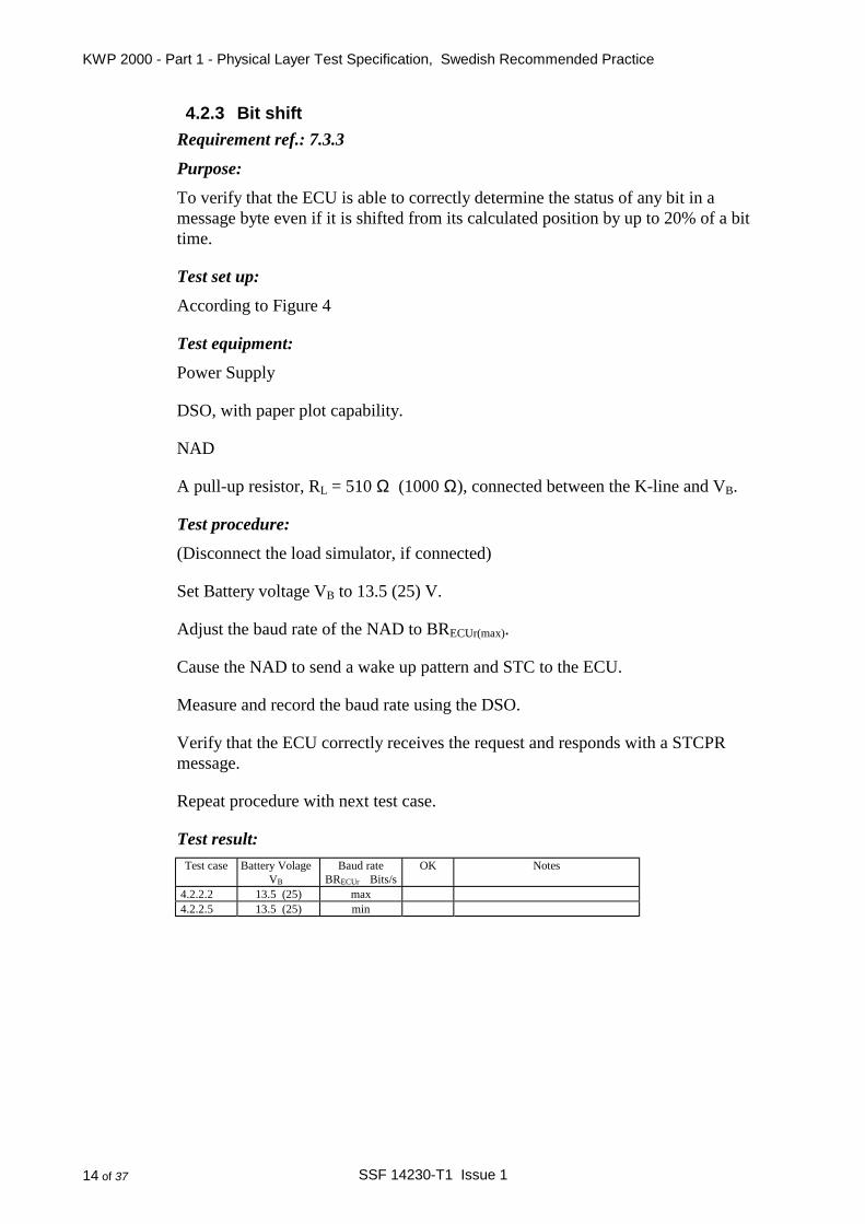
4.2.3 Bit shift
Requirement ref.: 7.3.3
Purpose:
To verify that the ECU is able to correctly determine the status of any bit in amessage byte even if it is shifted from its calculated position by up to 20% of a bittime.
Test set up:
According to Figure 4
Test equipment:
Power Supply
DSO, with paper plot capability.
NAD
A pull-up resistor, RL = 510 Ω (1000 Ω), connected between the K-line and VB.
Test procedure:
(Disconnect the load simulator, if connected)
Set Battery voltage VB to 13.5 (25) V.
Adjust the baud rate of the NAD to BRECUr(max).
Cause the NAD to send a wake up pattern and STC to the ECU.
Measure and record the baud rate using the DSO.
Verify that the ECU correctly receives the request and responds with a STCPRmessage.
Repeat procedure with next test case.
Test result:
Test case Battery VolageVB
Baud rateBRECUr Bits/s
OK Notes
4.2.2.2 13.5 (25) max4.2.2.5 13.5 (25) min

KWP 2000 - Part 1 - Physical Layer Test Specification, Swedish Recommended Practice
SSF 14230-T1 Issue 1 15 of 37
5 Test Tool tests
5.1 Electrical specification
5.1.1 Resistance test
Requirement ref.: 6.2.1
Purpose:
The test shall verify that the internal resistance (RTE ) between K-line and VB iswithin limits (Appendix 1).
Test set-up:
Figure 5
Test equipment:
Power Supply
DVM or DSO
Load resistor, RL = 510 Ω (1000 Ω), connected between K-line and SGND
Test procedure :
The Tester shall be disconnected from any ECU and be in receiving state.
Measure and connect the external load resistor RL between K-line and SGND.
Set Battery voltage VB to 13.5 (25) V.
Measure battery voltage (VB) and K-line voltage (VK ).
RTE = RL (VB /VK - 1)
Test result:
Measured values CalculatedVB V VK V RL Ω RTE Ω OK

KWP 2000 - Part 1 - Physical Layer Test Specification, Swedish Recommended Practice
SSF 14230-T1 Issue 116 of 37
5.1.2 Capacitance test
Requirement ref.: 6.2.6
Purpose:
The test shall verify that the capacitance of the Tester, including cables, does notexceed CTE(max).
Test set-up:
According to Figure 6.
Use short leads to reduce stray capacitances which will add to the measuredcapacitance.
Test equipment:
Power Supply
DSO
Signal Generator
Test procedure:
The Tester shall be disconnected from any ECU and be in receiving state.
Set Battery voltage VB to 13.5 (25) V.
Connect signal generator and DSO according to Figure 6.
Set up the signal generator to produce a square wave signal. Recommendedfrequency = 10 kHz and output voltage Vmax = 12 V (24 V)
Measure rise time and calculate the capacitance (if necessary adjust the signalfrequency). Use the measured value (test 5.1.1) of RTE in the calculation.
T
0,63 Vmax - VminVmax
Vmin
CTE = T / RTE
Verify that CTE < CTE(max)
Test result:
CTE(max) nF T µs CTE nF OK

KWP 2000 - Part 1 - Physical Layer Test Specification, Swedish Recommended Practice
SSF 14230-T1 Issue 1 17 of 37
5.1.3 Voltage transients
Requirement ref.: 6.2.4
Purpose:
Verify that voltage transients on the battery supply terminal are not transferred tothe open K-line.
The Tester shall not transfer voltage transients to the open K-line which mightadversely effect communication or harm other equipment connected to the line.Limits specified by SSF 14230-1 are positive voltages of VB or 40V, whichever isthe lower, and negative voltages of -1 V. Test method specified in ISO 7637-1(ISO 7637-2) applies.
Test set-up:
ISO 7637-1 (ISO 7637-2)
Test equipment:
TBD
Test procedure:
TBD
Test result:
TBD

KWP 2000 - Part 1 - Physical Layer Test Specification, Swedish Recommended Practice
SSF 14230-T1 Issue 118 of 37
5.2 Signal level tests
This test shall verify that the tester correctly interprets signal levels for logical ‘0’sand ‘1’s. A standard response message (Appendix 4) is composed at the NAD andtransmitted to the Tester on request.
Request messages from the Tester (transmitting state) are measured on the K-lineusing maximum sink current and capacitance.
Signal levels and slope times from the NAD (receiving state) are adjusted to giveproper test conditions on the K-line.
The tests shall be run at nominal and extreme battery voltages.
5.2.1 Transmission state
Requirement ref.: 5.1, 6.2.1, 6.2.2
Purpose:
To verify that the Tester is capable of supplying appropriate signal levels, slopetimes and baudrate at max load and under various battery voltage conditions.
Test set-up:
According to Figure 7.
Test equipment:
Power Supply
DSO
NAD
An adjustable pull-up resistor, RV ,with variable resistance between 0 - 200 Ω ,connected between the K-line and VB.
An adjustable load resistor, ROB , connected between the K-line and SGND. Thevalue of ROB shall be selectable:
ROB(min) = 5.0 kΩ (10 kΩ), or ROB(max) = 126 kΩ (231 kΩ).
A capacitance, COB = 7.2 nF (5.0 nF), connected between the K-line and SGND.
Test procedure:
Set Battery voltage VB to 8 (16) Volt.
1) Connect ROB(max) between the K-line and SGND.
Cause the Tester to send STC to the NAD
KWP 2000 - Part 1 - Physical Layer Test Specification, Swedish Recommended Practice
SSF 14230-T1 Issue 1 19 of 37
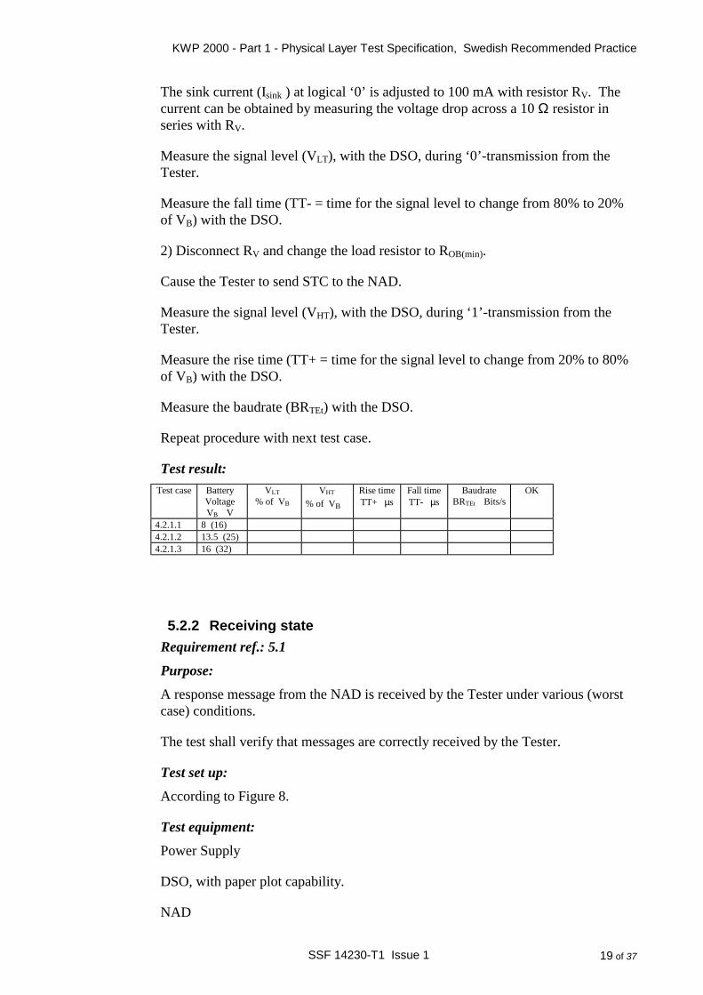
The sink current (Isink ) at logical ‘0’ is adjusted to 100 mA with resistor RV. Thecurrent can be obtained by measuring the voltage drop across a 10 Ω resistor inseries with RV.
Measure the signal level (VLT), with the DSO, during ‘0’-transmission from theTester.
Measure the fall time (TT- = time for the signal level to change from 80% to 20%of VB) with the DSO.
2) Disconnect RV and change the load resistor to ROB(min).
Cause the Tester to send STC to the NAD.
Measure the signal level (VHT), with the DSO, during ‘1’-transmission from theTester.
Measure the rise time (TT+ = time for the signal level to change from 20% to 80%of VB) with the DSO.
Measure the baudrate (BRTEt) with the DSO.
Repeat procedure with next test case.
Test result:
Test case BatteryVoltageVB V
VLT
% of VB
VHT
% of VB
Rise timeTT+ µs
Fall timeTT- µs
BaudrateBRTEt Bits/s
OK
4.2.1.1 8 (16)4.2.1.2 13.5 (25)4.2.1.3 16 (32)
5.2.2 Receiving state
Requirement ref.: 5.1
Purpose:
A response message from the NAD is received by the Tester under various (worstcase) conditions.
The test shall verify that messages are correctly received by the Tester.
Test set up:
According to Figure 8.
Test equipment:
Power Supply
DSO, with paper plot capability.
NAD

KWP 2000 - Part 1 - Physical Layer Test Specification, Swedish Recommended Practice
SSF 14230-T1 Issue 120 of 37
Load simulator.

KWP 2000 - Part 1 - Physical Layer Test Specification, Swedish Recommended Practice
SSF 14230-T1 Issue 1 21 of 37
Test procedure:
Voltage levels and waveforms are measured and recorded with a DSO.
Set Battery voltage VB to 8 V (16 V).
Adjust signal levels and slope times on the K-line, when the NAD is transmitting,using the load simulator, to
VLR(max) for logical ‘0’ and to VHR(min) for logical ‘1’TT+(max) and TT-(max)
Slope times are defined as the time for the signal level to change from 20% to 80%(rise time) and from 80% to 20% (fall time) of VB.
Cause Tester to initialize and send STC to the NAD.
The NAD shall send STCPR after the time P2. Default lower time for P2 (25 ms)shall be used.
Measure signal levels and slope times using the DSO. Waveforms for each test caseshall be recorded.
Verify that the Tester correctly receives the response message.
Repeat procedure with next test case.
Test result:
Test case Battery VoltageVB
OK Notes
4.2.2.1 8 (16)4.2.2.2 13.5 (25)4.2.2.3 16 (32)
5.2.3 Bit shift
Requirement ref.: 6.2.3
Purpose:
To verify that the diagnostic tester is able to correctly determine the status of anybit in a message byte even if it is shifted from its calculated position by up to 30%of a bit time.
Test set up:
According to Figure 8
Test equipment:
Power Supply
DSO, with paper plot capability.
NAD

KWP 2000 - Part 1 - Physical Layer Test Specification, Swedish Recommended Practice
SSF 14230-T1 Issue 122 of 37
Test procedure:
(Disconnect the load simulator, if connected)
Set Battery voltage VB to 13.5 (25) V.
Adjust the baud rate of the NAD to BRTEr(max).
Cause Tester to initialize and send STC to the NAD.
The NAD shall send STCPR after the time P2. Default lower time for P2 (25 ms)shall be used.
Measure and record the baud rate using the DSO.
Verify that the Tester correctly receives the response message.
Repeat procedure with next test case.
Test result:
Test case Battery VolageVB
Baud rateBRTEr Bits/s
OK Notes
4.2.2.2 13.5 (25) max4.2.2.5 13.5 (25) min

KWP 2000 - Part 1 - Physical Layer Test Specification, Swedish Recommended Practice
SSF 14230-T1 Issue 1 23 of 37
6 Appendix
Appendix 1. Parameter values
Parameter Symbol Min Max Units NotesHigh Receive Threshold VHR 0.7 VB VB VHigh Transmit Threshold VHT 0.8 VB VLow Receive Threshold VLR 0.2 VB VLow Transmit Threshold VLT 0.1 VB VTester Bus Line Capacitance CTE 0 2 nFTester Bus Line Resistance to VB RTE 485 (950) 535
(1050)Ω
Rise Time TT+ 0 9.6 (14.4) µs
Fall Time TT- 0 9.6 (14.4) µs
Tester Bit Rate, transmitting BRTEt 10348 10452 bits/s 10400 ± 0.5%Tester Bit Rate, receiving BRTEr 10088 10712 bits/s 10400 ± 3%ECU Bus Line Capacitance CECU 0 Vehicle
manufact.specific
pF
ECU Bus Line Resistance toSGND, transmitting ‘0’
RECU(0) 110 Ω
ECU Bus Line Resistance toSGND, transmitting ‘1’, receiving
RECU(1) Vehiclemanufact.specific
kΩ
Vehicle Bus Line Resistance to VB R+OB 100 kΩVehicle Bus Line Resistance toSGND
R-OB 5 (10) kΩ
Total Bus Line Capacitance CTot 0 9.2 (7.0) nF
ECU bitrate,transmitting
BRECUt 10223(10296)
10577(10504)
bits/s 10400 ± 1.7% (± 1.0%)
ECU bitrate,receiving
BRECUr 10192(10192)
10608(10608)
bits/s 10400 ± 2% (± 2%)
Tester current sink capability Isink 100 mAOver voltage, permanent VOVp 20 (36)Over voltage, 30 min VOV30 24 (42)Over voltage, 1 min VOV1 30 (48)Over voltage, max positive V+ISO 40 (60)Over voltage, max negaitve V-ISO -1 (-1)

KWP 2000 - Part 1 - Physical Layer Test Specification, Swedish Recommended Practice
SSF 14230-T1 Issue 124 of 37
Appendix 2 Figures
PS ECU
DSO
+
VB
-
+VK
-
RL
Signal GND
K-line
Chassis GND
J1962 connector:a=16, b=7, c=5, d=4
a
b
c
d
DUT
Figure 1
PS ECU
DSOSG
+VK
-
+
VB
-
D
RL
Signal GND
K-line
Chassis GND
J1962 connector:a=16, b=7, c=5, d=4
a
b
c
d
DUT
Figure 2

KWP 2000 - Part 1 - Physical Layer Test Specification, Swedish Recommended Practice
SSF 14230-T1 Issue 1 25 of 37
PS ECU
DSO
+
VB
-
+VK
-
COB ROBSignal GND
K-line
Chassis GND
J1962 connector:a=16, b=7, c=5, d=4
a
b
c
d
DUT
RV
K-line to RS232converter
RS232 to K-lineconverter
Com X Com Y
PC
NAD
Figure 3
ECU
DSO
+VK
-PS
+
VB
-
Signal GND
K-line
Chassis GND
J1962 connector:a=16, b=7, c=5, d=4
a
b
c
d
DUT
K-line to RS232converter
RS232 to K-lineconverter
Com X Com Y
PC
LoadSimulator
RL
NAD
Figure 4

KWP 2000 - Part 1 - Physical Layer Test Specification, Swedish Recommended Practice
SSF 14230-T1 Issue 126 of 37
PSTestTool
DSO
+
VB
-
+VK
-
RLSignal GND
K-line
Chassis GND
J1962 connector:a=16, b=7, c=5, d=4
a
b
c
d
DUT
Figure 5
PSTestTool
SG DSO
+VK
-
+
VB
-
Signal GND
K-line
Chassis GND
J1962 connector:a=16, b=7, c=5, d=4
a
b
c
d
DUT
Figure 6

KWP 2000 - Part 1 - Physical Layer Test Specification, Swedish Recommended Practice
SSF 14230-T1 Issue 1 27 of 37
PSTestTool
DSO
+
VB
-
+VK
-
ROBSignal GND
K-line
Chassis GND
J1962 connector:a=16, b=7, c=5, d=4
a
b
c
d
DUT
10 ΩRV
K-line to RS232converter
RS232 to K-lineconverter
Com X Com Y
PC
NAD
COB
Figure 7
TestTool
DSO
+VK
-PS
+
VB
-
Signal GND
K-line
Chassis GND
J1962 connector:a=16, b=7, c=5, d=4
a
b
c
d
DUT
K-line to RS232converter
RS232 to K-lineconverter
Com X Com Y
PC
LoadSimulator
NAD
Figure 8

KWP 2000 - Part 1 - Physical Layer Test Specification, Swedish Recommended Practice
SSF 14230-T1 Issue 128 of 37
Appendix 3. Test Equipment
The accuracy of the test equipment actually used for the tests shall be stated in thetest report.
Equipment Functional requirements Accuracy
Power Supply 0-16 V (0-32 V) ± 100 mV
DSO Paper plot ± 100 mV± 1 µs
DVM ± 100 mV± 1 % for resistancemeasurements
Signal Generator The signal generator shall be capable ofsupplying an output voltage of about 12V(24 V)
Resistor RECU(1) (spec value)
Resistor 510 Ω (1000 Ω)
Resistor 1 kΩ
Diode 1 A
Adjustable resistor Variable resistance between 485 - 535 Ω(950 - 1050 Ω)
Adjustable resistor Variable resistance between 0 - 200 Ω
Adjustable resistor The value shall be such that the totalresistance between the K-line and SGNDis 5 kΩ (10 kΩ)
Adjustable resistor selectable: 5.0 kΩ (10 kΩ), or 126 kΩ(231 kΩ).
Capacitance Typical: 8.2 nF (6.8 nF)
Capacitance 7.2 nF (5.0 nF)
KWP 2000 - Part 1 - Physical Layer Test Specification, Swedish Recommended Practice
SSF 14230-T1 Issue 1 29 of 37
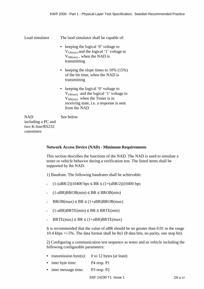
Load simulator The laod simulator shall be capable of:
• keeping the logical ‘0’ voltage toVLR(max) and the logical ‘1’ voltage toVHR(min) , when the NAD istransmitting
• keeping the slope times to 10% (15%)of the bit time, when the NAD istransmitting
• keeping the logical ‘0’ voltage toVLR(max) and the logical ‘1’ voltage toVHR(min) when the Tester is inreceiving state, i.e. a response is sentfrom the NAD
NADincluding a PC andtwo K-line/RS232converters
See below
Network Access Device (NAD) - Minimum Requirements
This section describes the functions of the NAD. The NAD is used to simulate atester or vehicle behavior during a verification test. The listed items shall besupported by the NAD:
1) Baudrate. The following baudrates shall be achievable:
• (1-(aBR/2))10400 bps ≤ BR ≤ (1+(aBR/2))10400 bps
• (1-aBR)BROB(min) ≤ BR ≤ BROB(min)
• BROB(max) ≤ BR ≤ (1+aBR)BROB(max)
• (1-aBR)BRTE(min) ≤ BR ≤ BRTE(min)
• BRTE(max) ≤ BR ≤ (1+aBR)BRTE(max)
It is recommended that the value of aBR should be no greater than 0.01 in the range10.4 kbps +/-5%. The data format shall be 8n1 (8 data bits, no parity, one stop bit).
2) Configuring a communication test sequence as tester and as vehicle including thefollowing configurable parameters:
• transmission byte(s): 0 to 12 bytes (at least)
• inter byte time: P4 resp. P1
• inter message time: P3 resp. P2

KWP 2000 - Part 1 - Physical Layer Test Specification, Swedish Recommended Practice
SSF 14230-T1 Issue 130 of 37
• Target and Source address bytes
3) Running any predefined test sequence (see Appendix 4).
4) Time stamping of received/transmitted bytes with an accuracy and a resolutionof at least 0.1 ms.
5) Storing and/or displaying the bytes and affiliated time stamps.
6) Bus Line Voltage. The following voltages shall be achievable:
• (1-aV)VHRx(min) ≤ V ≤ VHRx(min)
• (1-aV)VHTx(min) ≤ V ≤ VHTx(min)
• VLRx(max) ≤ V ≤ (1+aV)VLRx(max)
• VLTxTE(max) ≤ V ≤ (1+aV)VLTxTE(max)
• VLTxOB(max) ≤ V ≤ (1+aV)VLTxOB(max)
It is recommended that the value of aV should be no greater than 0.01.
• (VHRx(min)-DNAD) ± DNAD
• (VHTx(min)-DNAD) ± DNAD
• (VLRx(max)+DNAD) ± DNAD
• (VLTxTE(max)+DNAD) ± DNAD
• (VLTxOB(max)+DNAD) ± DNAD
The voltage level for the DNAD should be ≤ 0.1V
7) Adjusting the electrical parameters. The voltage levels for transmission shall beadjustable with a resolution and accuracy of 0.1 V. The logical high and low levelsshall be configurable independently. The transition times shall be also adjustableindependently with a resolution and an accuracy of 1% in the range between 0 and10% bit time.
8) All time values shall be configurable with an accuracy and a resolution of at least0.1 ms.

KWP 2000 - Part 1 - Physical Layer Test Specification, Swedish Recommended Practice
SSF 14230-T1 Issue 1 31 of 37
Appendix 4. Test Messages
The following test messages shall be used in the communication between the NADand the DUT. The messages are composed as standard Keyword Protocol 2000messages, as defiend in SSF 14230-2 and SSF 14230-3
String starting with # contains message number and info text, e.g. to be displayedon test tool and in logfile (comments are preceeded by //).
Strings enclose by contain the actual message string in hexadecimal notation,checksum excluded.
xx = DUT diagnostic addressfx = Test Tool diagnostic address
startCommunicationRequest
#1 STC
81 xx fx 81
startCommunicationPositiveResponse
#2 STCPR, 4 byte header, Keyword 2026
80 fx xx 03 c1 ea 8f
stopCommunicationRequest
#3 SPC, 4 bytes header
80 xx fx 01 82
stopCommunicationPositiveResponse
#4 SPCPR, 4 bytes header
80 fx xx 01 c2

KWP 2000 - Part 1 - Physical Layer Test Specification, Swedish Recommended Practice
SSF 14230-T1 Issue 132 of 37
readDataByLocalIDRequest
#5 RDBLI, LI=01, 4 bytes header
80 fx xx 02 21 01
readDataByLocalIDPositiveResponse
#6 RDBLIPR, LI=01, 4 bytes header, 10 bytes data
80 fx xx 0a 61 01 30 31 32 33 34 35 36 37

KWP 2000 - Part 1 - Physical Layer Test Specification, Swedish Recommended Practice
SSF 14230-T1 Issue 1 33 of 37
Appendix 5. Test Results Summary
DUT identification
Test Equipment
Equipment No. Accuracy
Power Supply
DSO
DVM
Signal Generator
NAD
Load simulator
KWP 2000 - Part 1 - Physical Layer Test Specification, Swedish Recommended Practice
SSF 14230-T1 Issue 134 of 37
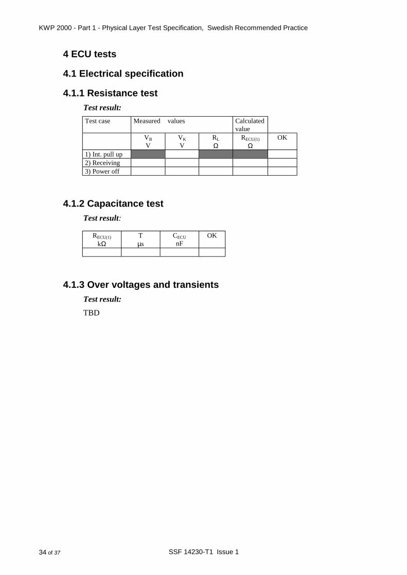
4 ECU tests
4.1 Electrical specification
4.1.1 Resistance test
Test result:
Test case Measured values Calculatedvalue
VB
VVK
VRL
ΩRECU(1)
ΩOK
1) Int. pull up2) Receiving3) Power off
4.1.2 Capacitance test
Test result:
RECU(1)
kΩTµs
CECU
nFOK
4.1.3 Over voltages and transients
Test result:
TBD
KWP 2000 - Part 1 - Physical Layer Test Specification, Swedish Recommended Practice
SSF 14230-T1 Issue 1 35 of 37
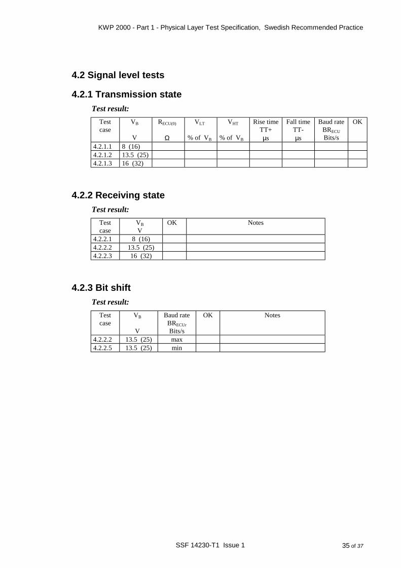
4.2 Signal level tests
4.2.1 Transmission state
Test result:
Testcase
VB
V
RECU(0)
Ω
VLT
% of VB
VHT
% of VB
Rise timeTT+µs
Fall timeTT-µs
Baud rateBRECU
Bits/s
OK
4.2.1.1 8 (16)4.2.1.2 13.5 (25)4.2.1.3 16 (32)
4.2.2 Receiving state
Test result:
Testcase
VB
VOK Notes
4.2.2.1 8 (16)4.2.2.2 13.5 (25)4.2.2.3 16 (32)
4.2.3 Bit shift
Test result:
Testcase
VB
V
Baud rateBRECUr
Bits/s
OK Notes
4.2.2.2 13.5 (25) max4.2.2.5 13.5 (25) min

KWP 2000 - Part 1 - Physical Layer Test Specification, Swedish Recommended Practice
SSF 14230-T1 Issue 136 of 37
5 Test Tool tests
5.1 Electrical specification
5.1.1 Resistance test
Test result:
Measured values CalculatedVB
VVK
VRL
ΩRTE
ΩOK
5.1.2 Capacitance test
Test result:
CTE(max)
nFTµs
CTE
nFOK
5.1.3 Voltage transients
Test result:
TBD

KWP 2000 - Part 1 - Physical Layer Test Specification, Swedish Recommended Practice
SSF 14230-T1 Issue 1 37 of 37
5.2 Signal level tests
5.2.1 Transmission state
Test result:
Testcase
VB
V
VLT
% of VB
VHT
% of VB
Rise timeTT+µs
Fall timeTT-µs
BaudrateBRTEt
Bits/s
OK
4.2.1.1 8 (16)4.2.1.2 13.5 (25)4.2.1.3 16 (32)
5.2.2 Receiving state
Test result:
Testcase
VB
VOK Notes
4.2.2.1 8 (16)4.2.2.2 13.5 (25)4.2.2.3 16 (32)
5.2.3 Bit shift
Test result:
Testcase
VB
V
Baud rateBRTEr
Bits/s
OK Notes
4.2.2.2 13.5 (25) max4.2.2.5 13.5 (25) min