sri krishna institute of technology, bengaluru-560090
TRANSCRIPT
LABORATORY PLAN - CAY 2019 BE-5-EE-SKIT-Ph5b1-F02-V2.2
Sri Krishna Institute of Technology, Bengaluru-560090
COURSE PLAN
Academic Year - 2019-2020
Academic Evaluation and Monitoring Cell
Program: BE- Electrical and Electronics Engineering
Semester: 3
Course Code: 18EEL38
Course Title: Electronics Laboratory
Credit/L-T-P: 2 / 0-2-2
Total Contact Hours: 40
Course Plan Author: Avinash S
#29, Hesaragatta Main Road, Chimney Hills
Chikkabanavara Post Bengaluru – 560090, Karnataka, India
Phone / Fax :080-23721477/28392221/23721315
Web: www,skit.org, e-mail:
18EEL38 Copyright ©2017. cAAS. All rights reserved.Page # 1 / 29
Ref No:
LABORATORY PLAN - CAY 2019 BE-5-EE-SKIT-Ph5b1-F02-V2.2
Table of ContentsA. LABORATORY INFORMATION............................................................................................................................................. 4
1. Laboratory Overview.................................................................................................................................................................................... 42. Laboratory Content....................................................................................................................................................................................... 43. Laboratory Material....................................................................................................................................................................................... 54. Laboratory Prerequisites:......................................................................................................................................................................... 55. Content for Placement, Profession, HE and GATE................................................................................................................ 5
B. Laboratory Instructions............................................................................................................................................................. 61. General Instructions...................................................................................................................................................................................... 62. Laboratory Specific Instructions......................................................................................................................................................... 6
C. OBE PARAMETERS....................................................................................................................................................................... 61. Laboratory Outcomes................................................................................................................................................................................. 62. Laboratory Applications............................................................................................................................................................................ 73. Mapping And Justification....................................................................................................................................................................... 84. Articulation Matrix.......................................................................................................................................................................................... 85. Curricular Gap and Experiments......................................................................................................................................................... 96. Experiments Beyond Syllabus............................................................................................................................................................. 9
D. COURSE ASSESSMENT.......................................................................................................................................................... 101. Laboratory Coverage................................................................................................................................................................................ 102. Continuous Internal Assessment (CIA)......................................................................................................................................... 10
E. EXPERIMENTS................................................................................................................................................................................ 11Experiment 01 : Structure of C program........................................................................................................................................... 11Experiment 02 : Keywords and identifiers...................................................................................................................................... 12Experiment 03 : ………........................................................................................................................................................................................... 13Experiment 04 : ………........................................................................................................................................................................................... 13
F. Content to Experiment Outcomes.................................................................................................................................. 141. TLPA Parameters.......................................................................................................................................................................................... 142. Concepts and Outcomes:...................................................................................................................................................................... 15
INSTRUCTIONS TO TEACHERS• Classroom / Lab activity shall be started after taking attendance.• Attendance shall only be signed in the classroom by students.• Three hours attendance should be given to each Lab. • Use only Blue or Black Pen to fill the attendance. • Attendance shall be updated on-line & status discussed in DUGC.• No attendance should be added to late comers. • Modification of any attendance, over writings, etc is strictly prohibited. • Updated register is to be brought to every academic review meeting as per the COE.
Note : Remove “Table of Content” before including in CP Book
18EEL38 Copyright ©2017. cAAS. All rights reserved.Page # 2 / 29
LABORATORY PLAN - CAY 2019 BE-5-EE-SKIT-Ph5b1-F02-V2.2
18EEL38 : ELECTRONICS LABORATORY
A. LABORATORY INFORMATION
1. Lab OverviewDegree: B.Tech Program: EEYear / Semester : 2 / 3 Academic Year: 2019Course Title: Electronics Laboratory Course Code: 18EEL38Credit / L-T-P: 2 / 0-2-2 SEE Duration: 180 MinutesTotal Contact Hours: 40Hrs SEE Marks: 60 MarksCIA Marks: 40 Assignment 1 / Module
Course Plan Author: Mr. Avinash S Sign Dt :
Checked By: Sign Dt :
2. Lab ContentUnit Title of the Experiments Lab
HoursConcept Blooms
Level1 Design and Testing of Full wave – centre tapped transformer type
and Bridge type rectifier circuits withand without Capacitor filter.Determination of ripple factor, regulation and efficiency.
3 Rectification L5
2 Static Transistor characteristics for CE, CB and CC modes anddetermination of h parameters.
3 Characteristics
L3
3 Frequency response of single stage BJT and FET RC coupled amplifier and determination of half power points,bandwidth, input and output impedances.
3 FrequencyResponse
L4
4 Design and testing of BJT - RC phase shift oscillator for given frequency of oscillation.
3 SignalGeneration
L5
5 Determination of gain, input and output impedance of BJT Darlington emitter follower with and without bootstrapping
3 Small signalanalyses ofDarlington
emitterfollower
L3
6 Simplification, realization of Boolean expressions using logic gates/Universal gates.
3 Realization L3
7 Realization of half/Full adder and Half/Full Sub tractors usinglogic gates
3 Realization L3
8 Realization of parallel adder/Sub tractors using 7483 chip- BCDto Excess-3 code conversion and Vice - Versa.
3 Realization L3
9 Realization of Binary to Gray code conversion and vice versa 3 Realization L310 Design and testing Ring counter/Johnson counter 3 Counter
DesignL5
11 Design and testing of Sequence generator 3 Sequence generator
L5
12 Realization of 3 bit counters as a sequential circuit and MOD – Ncounter design using 7476, 7490, 74192, 74193
3 MOD – NCounterDesign
L5
3. Lab MaterialUnit Details Available
1 Text books
18EEL38 Copyright ©2017. cAAS. All rights reserved.Page # 3 / 29
LABORATORY PLAN - CAY 2019 BE-5-EE-SKIT-Ph5b1-F02-V2.2
Digital Logic Applications and Design by John M Yarbrough & Donald DGivone,Electronic Devices and CircuitTheory by Robert L Boylestad LouisNashelsky & Electronic Devices and Circuits by David A Bell.
In Lib
2 Reference booksLogic and computer design Fundamentals by M. Morries Mano and CharlesKime, Fundamentals of logic design byCharles H Roth, JR and Larry L. Kinney,Fundamentals of Digital Circuits by A. Anand Kumar , A Text Book of ElectricalTechnology, Electronic Devices and Circuits by B.L. Theraja, A.K. Theraja,Electronic Devices and Circuits by Anil K. Maini VashaAgarval & Fundamentalsof Analog Circuits by Thomas L Floyd.
In dept
3 Others (Web, Video, Simulation, Notes etc.)Not Available
4. Lab Prerequisites:- - Base Course: - -
SNo CourseCode
Course Name Topic / Description Sem Remarks
1 17ELN24 Basic Electronics 1. Knowledge Digital Electronics Fundamentals
2
Note: If prerequisites are not taught earlier, GAP in curriculum needs to be addressed. Include inRemarks and implement in B.5.
5. General InstructionsSNo Instructions Remarks
1 Keep the lab neatly. Maintain silence.2 Maintain your lab observation and lab manual.3 Prepare your experiment in well advance.4 Check the power supply before use.5 Maintain discipline in the lab.6 After completion of your experiment switch off the power supply.7 Observation book and Lab record are compulsory.8 Students should report to the concerned lab as per the time table.9 After completion of the experiment, certification of the concerned staff in-
charge in the observation book is necessary.10 Student should bring a notebook of 100 pages and should enter the
readings /observations into the notebook while performing the experiment.
6. Lab Specific InstructionsSNo Specific Instructions Remarks
1 Students are expected to study the circuit, theory and procedures,expected output before doing the experiment.
2 Adjustment of signal generator: - Before connecting the signal generator tothe circuit check the followings. a. Set the shape of the waveform (sinusoidal), b. Set the frequency using coarse and fine adjustments. c. Set the offset adjustments. Set the CRO in DC mode and ensure thewaveform is symmetry in both positive and negative cycle. If not , adjust itusing the DC offsetting potentiometerd. Set the voltage magnitude using Vcourse settings and Vfine adjustments.
3 Adjustment of CRO: a. Select the right voltage and time scale to get the proper waveform b. For clipper and clamper circuits, observe the waveform in DC mode onlyc. Set the input waveform mainly for offset setting in DC mode only. d. Before measurement, ensure X & Y are in calibrated mode (if providedexternally)e. Ensure that Channel selection and trigger mode are properly set.
18EEL38 Copyright ©2017. cAAS. All rights reserved.Page # 4 / 29

LABORATORY PLAN - CAY 2019 BE-5-EE-SKIT-Ph5b1-F02-V2.2
f. In case of two channels do not mix the signal and ground terminals 4 Multi-meter adjustments:-
a. Set the right mode before taking the readings. b. For current reading, connect the multimeter in mA (or A) mode to thecircuit before switching on the supply. Do not remove the current meterwhen the supply is on. Check for ac and dc modes as required. c. For voltage reading ensure that proper ac or dc setting.d. Use the proper leads for the measurement. Wrong cables damage theinstrument.
5 After adjusting the input voltage, check the circuit connections beforeturning the power on.
6 After adjusting the input voltage, check the circuit connections beforeturning the power on.
7 Don’t pull out the connections with the power supply on. 8 Wear your College ID card Do not operate the IC trainer kits without
permission 9 Avoid loose connection and short circuits 10 Do not interchange the ICs while doing the experiment 11 Handle the trainer kit properly 12 Do not panic if you do not get the output 13 After completion of the experiment switch off the power and return the
components
B. OBE PARAMETERS
1. Lab / Course Outcomes # COs Teach.
HoursConcept Instr
MethodAssessment
MethodBlooms’
Level1 Design & Analyses of Full wave Rectifiers
using hardware components03 Rectification Conduct
ionTest & Viva
VoceL5
2 Determine Characteristic of CE, CB & CCmodes of h parameters using hardwarecomponents
03 Characteristics
Conduction
Test & VivaVoce
L3
3 Analyze the frequency response of BJT &FET using using hardware components
03 FrequencyResponse
Conduction
Test & VivaVoce
L4
4 Analyses & Design of BJT-RC phase shiftof oscillator for given fequency usingusing hardware components
03 SignalGeneration
Conduction
Test & VivaVoce
L5
5 Determine the gain, i/p & o/p of BJTusing hardware components
03 Small signalanalyses ofDarlington
emitterfollower
Conduction
Test & VivaVoce
L3
6 Realize the Boolean expression with their truth table using LD trainer kit.
03 Realization Conduction
Test & VivaVoce
L3
7 Realize the Adders & Substractors withtheir truth table using LD trainer kit.
03 Realization Conduction
Test & VivaVoce
L3
8 Realize the parallel adder/Subtractorswith their truth table using LD trainer kit.
03 Realization Conduction
Test & VivaVoce
L3
9 Realize the Binary to Gray code & viceversa using LD trainer kit.
03 Realization Conduction
Test & VivaVoce
L3
10 Design & Realize the Ring & Jogn counterusing LD trainer kit.
03 CounterDesign
Conduction
Test & VivaVoce
L5
11 Design & Realize the Sequence generatorusing LD trainer kit.
03 Sequence generator
Conduction
Test & VivaVoce
L5
12 Design & Realize the MOD – N CounterDesign using LD trainer kit.
03 MOD – NCounterDesign
Conduction
Test & VivaVoce
L5
- Total 36 - - - -
18EEL38 Copyright ©2017. cAAS. All rights reserved.Page # 5 / 29
LABORATORY PLAN - CAY 2019 BE-5-EE-SKIT-Ph5b1-F02-V2.2Note: Identify a max of 2 Concepts per unit. Write 1 CO per concept.
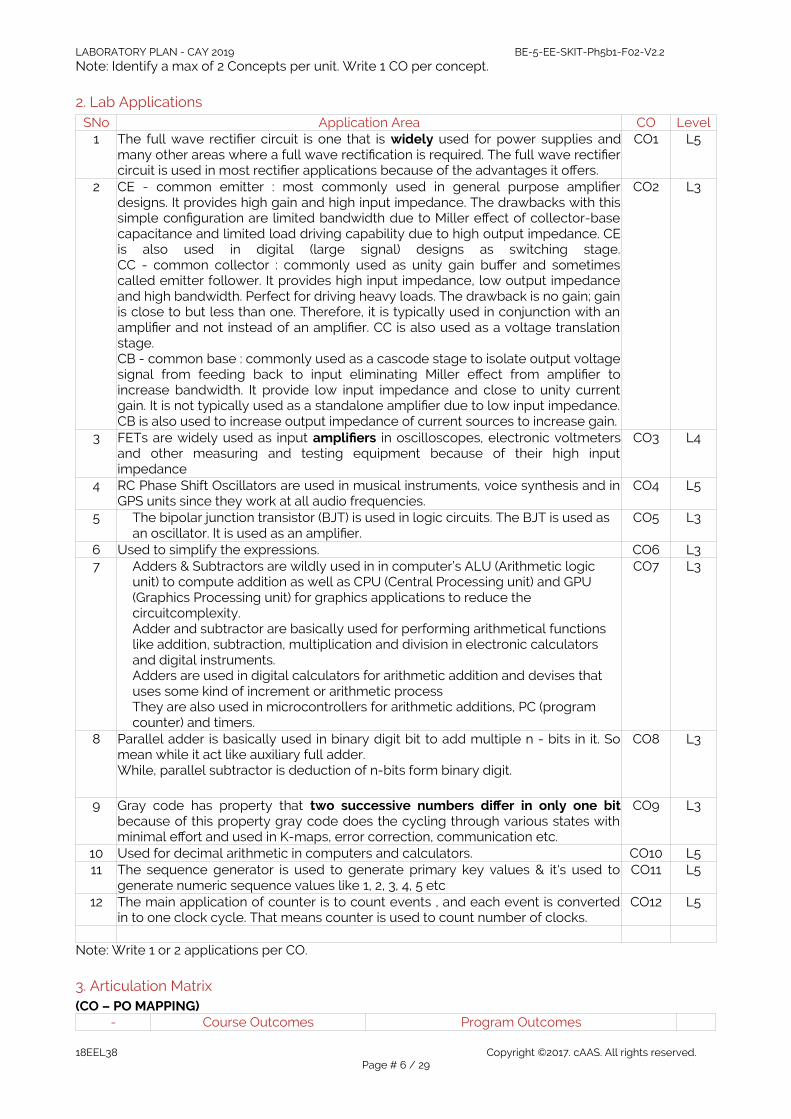
2. Lab ApplicationsSNo Application Area CO Level
1 The full wave rectifier circuit is one that is widely used for power supplies andmany other areas where a full wave rectification is required. The full wave rectifiercircuit is used in most rectifier applications because of the advantages it offers.
CO1 L5
2 CE - common emitter : most commonly used in general purpose amplifierdesigns. It provides high gain and high input impedance. The drawbacks with thissimple configuration are limited bandwidth due to Miller effect of collector-basecapacitance and limited load driving capability due to high output impedance. CEis also used in digital (large signal) designs as switching stage.CC - common collector : commonly used as unity gain buffer and sometimescalled emitter follower. It provides high input impedance, low output impedanceand high bandwidth. Perfect for driving heavy loads. The drawback is no gain; gainis close to but less than one. Therefore, it is typically used in conjunction with anamplifier and not instead of an amplifier. CC is also used as a voltage translationstage. CB - common base : commonly used as a cascode stage to isolate output voltagesignal from feeding back to input eliminating Miller effect from amplifier toincrease bandwidth. It provide low input impedance and close to unity currentgain. It is not typically used as a standalone amplifier due to low input impedance.CB is also used to increase output impedance of current sources to increase gain.
CO2 L3
3 FETs are widely used as input amplifiers in oscilloscopes, electronic voltmetersand other measuring and testing equipment because of their high inputimpedance
CO3 L4
4 RC Phase Shift Oscillators are used in musical instruments, voice synthesis and inGPS units since they work at all audio frequencies.
CO4 L5
5 The bipolar junction transistor (BJT) is used in logic circuits. The BJT is used as an oscillator. It is used as an amplifier.
CO5 L3
6 Used to simplify the expressions. CO6 L37 Adders & Subtractors are wildly used in in computer’s ALU (Arithmetic logic
unit) to compute addition as well as CPU (Central Processing unit) and GPU (Graphics Processing unit) for graphics applications to reduce the circuitcomplexity.Adder and subtractor are basically used for performing arithmetical functions like addition, subtraction, multiplication and division in electronic calculators and digital instruments.Adders are used in digital calculators for arithmetic addition and devises that uses some kind of increment or arithmetic processThey are also used in microcontrollers for arithmetic additions, PC (program counter) and timers.
CO7 L3
8 Parallel adder is basically used in binary digit bit to add multiple n - bits in it. Somean while it act like auxiliary full adder.While, parallel subtractor is deduction of n-bits form binary digit.
CO8 L3
9 Gray code has property that two successive numbers differ in only one bitbecause of this property gray code does the cycling through various states withminimal effort and used in K-maps, error correction, communication etc.
CO9 L3
10 Used for decimal arithmetic in computers and calculators. CO10 L511 The sequence generator is used to generate primary key values & it's used to
generate numeric sequence values like 1, 2, 3, 4, 5 etc CO11 L5
12 The main application of counter is to count events , and each event is convertedin to one clock cycle. That means counter is used to count number of clocks.
CO12 L5
Note: Write 1 or 2 applications per CO.
3. Articulation Matrix(CO – PO MAPPING)
- Course Outcomes Program Outcomes
18EEL38 Copyright ©2017. cAAS. All rights reserved.Page # 6 / 29
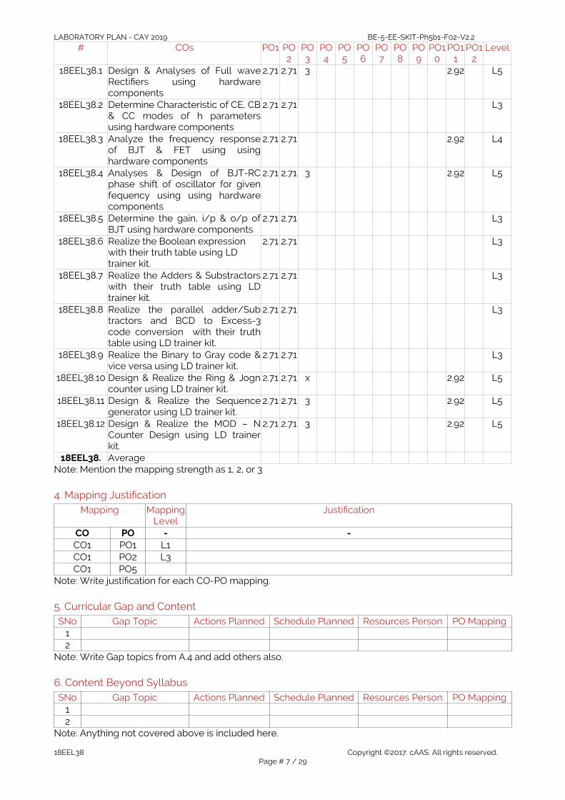
LABORATORY PLAN - CAY 2019 BE-5-EE-SKIT-Ph5b1-F02-V2.2
# COs PO1 PO2
PO3
PO4
PO5
PO6
PO7
PO8
PO9
PO10
PO11
PO12
Level
18EEL38.1 Design & Analyses of Full waveRectifiers using hardwarecomponents
2.71 2.71 3 2.92 L5
18EEL38.2 Determine Characteristic of CE, CB& CC modes of h parametersusing hardware components
2.71 2.71 L3
18EEL38.3 Analyze the frequency responseof BJT & FET using usinghardware components
2.71 2.71 2.92 L4
18EEL38.4 Analyses & Design of BJT-RCphase shift of oscillator for givenfequency using using hardwarecomponents
2.71 2.71 3 2.92 L5
18EEL38.5 Determine the gain, i/p & o/p ofBJT using hardware components
2.71 2.71 L3
18EEL38.6 Realize the Boolean expression with their truth table using LD trainer kit.
2.71 2.71 L3
18EEL38.7 Realize the Adders & Substractorswith their truth table using LDtrainer kit.
2.71 2.71 L3
18EEL38.8 Realize the parallel adder/Subtractors and BCD to Excess-3code conversion with their truthtable using LD trainer kit.
2.71 2.71 L3
18EEL38.9 Realize the Binary to Gray code &vice versa using LD trainer kit.
2.71 2.71 L3
18EEL38.10 Design & Realize the Ring & Jogncounter using LD trainer kit.
2.71 2.71 x 2.92 L5
18EEL38.11 Design & Realize the Sequencegenerator using LD trainer kit.
2.71 2.71 3 2.92 L5
18EEL38.12 Design & Realize the MOD – NCounter Design using LD trainerkit.
2.71 2.71 3 2.92 L5
18EEL38. AverageNote: Mention the mapping strength as 1, 2, or 3
4. Mapping JustificationMapping Mapping
LevelJustification
CO PO - -CO1 PO1 L1CO1 PO2 L3CO1 PO5
Note: Write justification for each CO-PO mapping.
5. Curricular Gap and ContentSNo Gap Topic Actions Planned Schedule Planned Resources Person PO Mapping
12
Note: Write Gap topics from A.4 and add others also.
6. Content Beyond SyllabusSNo Gap Topic Actions Planned Schedule Planned Resources Person PO Mapping
12
Note: Anything not covered above is included here.
18EEL38 Copyright ©2017. cAAS. All rights reserved.Page # 7 / 29
LABORATORY PLAN - CAY 2019 BE-5-EE-SKIT-Ph5b1-F02-V2.2
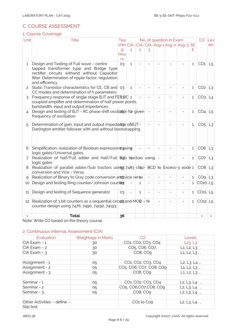
C. COURSE ASSESSMENT
1. Course CoverageUnit Title Tea
ching
Hours
No. of question in Exam CO LevelsCIA-
1CIA-
2CIA-
3Asg-1 Asg-2 Asg-3 SE
E
1 Design and Testing of Full wave – centretapped transformer type and Bridge typerectifier circuits withand without Capacitorfilter. Determination of ripple factor, regulationand efficiency.
03 1 - - - - - 1 CO1 L5
2 Static Transistor characteristics for CE, CB andCC modes and determination of h parameters.
03 1 - - - - - 1 CO2 L3
3 Frequency response of single stage BJT and FET RC coupled amplifier and determination of half power points,bandwidth, input and output impedances.
03 1 - - - - - 1 CO3 L4
4 Design and testing of BJT - RC phase shift oscillator for given frequency of oscillation.
03 1 - - - - - 1 CO4 L5
5 Determination of gain, input and output impedance of BJT Darlington emitter follower with and without bootstrapping
03 1 - - - - - 1 CO5 L3
6 Simplification, realization of Boolean expressions using logic gates/Universal gates.
03 1 - - - - - 1 CO6 L3
7 Realization of half/Full adder and Half/Full Sub tractors usinglogic gates
03 1 - - - - - 1 CO7 L3
8 Realization of parallel adder/Sub tractors using 7483 chip- BCD to Excess-3 codeconversion and Vice - Versa.
03 - 1 - - - - 1 CO8 L3
9 Realization of Binary to Gray code conversion and vice versa 03 - 1 - - - - 1 CO9 L310 Design and testing Ring counter/Johnson counter 03 - 1 - - - - 1 CO10 L5
11 Design and testing of Sequence generator 03 - 1 - - - - 1 CO11 L5
12 Realization of 3 bit counters as a sequential circuit and MOD – Ncounter design using 7476, 7490, 74192, 74193
03 - 1 - - - - 1 CO12 L5
- Total 36 - -Note: Write CO based on the theory course.
2. Continuous Internal Assessment (CIA)Evaluation Weightage in Marks CO Levels
CIA Exam – 1 30 CO1, CO2, CO3, CO4 L23, L3CIA Exam – 2 30 CO5, CO6, CO7, L1, L2, L3 . .CIA Exam – 3 30 CO8, CO9 L1, L2, L3 . .
Assignment - 1 05 CO1, CO2, CO3, CO4 L2, L3, L4 ...Assignment - 2 05 CO5, CO6, CO7, CO8, CO9 L1, L2, L3 ...Assignment - 3 05 CO8, CO9 L1, L2, L3 ...
Seminar - 1 05 CO1, CO2, CO3, CO4 L2, L3, L4 . ..Seminar - 2 05 CO5, CO6,CO7,CO8, CO9 L2, L3, L4 . ..Seminar - 3 05 CO8, CO9 L2, L3, L4 . ..
Other Activities – define –Slip test
CO1 to Co9 L2, L3, L4 . ..
18EEL38 Copyright ©2017. cAAS. All rights reserved.Page # 8 / 29
LABORATORY PLAN - CAY 2019 BE-5-EE-SKIT-Ph5b1-F02-V2.2
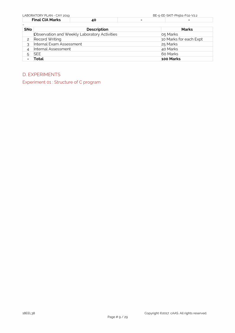
Final CIA Marks 40 - --SNo Description Marks
1Observation and Weekly Laboratory Activities 05 Marks2 Record Writing 10 Marks for each Expt3 Internal Exam Assessment 25 Marks4 Internal Assessment 40 Marks5 SEE 60 Marks- Total 100 Marks
D. EXPERIMENTS
Experiment 01 : Structure of C program
18EEL38 Copyright ©2017. cAAS. All rights reserved.Page # 9 / 29

LABORATORY PLAN - CAY 2019 BE-5-EE-SKIT-Ph5b1-F02-V2.2
# Experiment No.: 1 Marks DatePlanned
DateConducted
1 Title Design and Testing of Full wave – centre tapped transformer type andBridge type rectifier circuits with and without Capacitor filter.Determination of ripple factor, regulation and efficiency.
2 Course Outcomes Design & Analyses of Full wave Rectifiers using hardware components3 Aim Design and testing of Full wave and bridge type rectifier circuits with and
without capacitor and to determine ripple factor, regulation and efficiency 4 Material /
Equipment RequiredLab Manual/ CRO, Signal generator, capacitor, diodes, power chord, ameter,multi-meter, stepdown transformer.
5 Theory, Formula,Principle, Concept
The conversion of AC into pulsating DC is called Rectification. ElectronicDevices can convert AC power into DC power with high efficiency. The full-wave rectifier consists of a center-tapped transformer, which results in equalvoltages above and below the center-tap. During the positive half cycle, apositive voltage appears at the anode of D1 while a negative voltage appearsat the anode of D2. Due to this diode D1 is forward biased. It results a currentId1 through the load R.During the negative half cycle, a positive voltage appears at the anode of D2and hence it is forward biased, resulting a current Id2 through the load. At thesame instant a negative voltage appears at the anode of D1, reverse biasing itand hence it doesn’t conduct.
6 Procedure, Program,Activity, Algorithm,Pseudo Code
step 1: Rig up the circuit as per the circuit diagram shown.(without filter)
step 2:Switch ON the multimeter in DC mode & Switch ON the Power supply and measure Vdc and Idc
step 3: Now switch OFF the power supply & switch the multimeter in AC modeand switch ON the power supply to measure Vac and Iac. Calculate efficiency and Ripplefactor step 4:Rig up the circuit as per the circuit diagram shown.(with filter) step 5:Switch on the Power Supply and switch the multimeter in DC mode to measure Vdc and Idc step 6:Now switch the multimeter in AC mode and measure Iac step 7:Measure Vr(p-p) from CRO and calculate Vrms, efficiency and Ripplefactor.
7 Block, Circuit, ModelDiagram, ReactionEquation, ExpectedGraph
8 Observation Table,Look-up Table,Output
9 Sample Calculations Without filter: Let Vinrms = 12VVodc = 2Vm/π = 10.8v = 10vIodc = 100mA
18EEL38 Copyright ©2017. cAAS. All rights reserved.Page # 10 / 29
LABORATORY PLAN - CAY 2019 BE-5-EE-SKIT-Ph5b1-F02-V2.2
RL (min) = Vodc/Iodc = 100ΩLet Rf = 10ΩIorms = √Ioac2+Iodc2
With filter:Let Ripple = = Vorms /Vodc = 0.48γ = Vorms /Vodc = 0.48Let =6%=0.06, F = 50HZ and RL = 100 Ωγ = Vorms /Vodc = 0.48WKT = 1/4√3 F C RLγ = Vorms /Vodc = 0.48C = 470mFRipple factor = Voac/Vodc%Efficiency = Iodc2RL/Iorms2 (Rf+RL)%Regulation = (VNL-VFL)/VFL
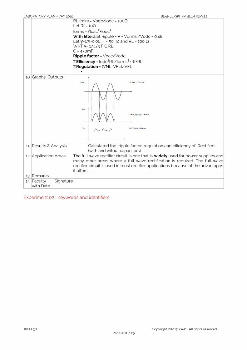
•10 Graphs, Outputs
11 Results & Analysis Calculated the ripple factor, regulation and efficiency of Rectifiers (with and witout capacitors)
12 Application Areas The full wave rectifier circuit is one that is widely used for power supplies andmany other areas where a full wave rectification is required. The full waverectifier circuit is used in most rectifier applications because of the advantagesit offers.
13 Remarks14 Faculty Signature
with Date
Experiment 02 : Keywords and identifiers
18EEL38 Copyright ©2017. cAAS. All rights reserved.Page # 11 / 29
LABORATORY PLAN - CAY 2019 BE-5-EE-SKIT-Ph5b1-F02-V2.2
- Experiment No.: 3 Marks DatePlanned
DateConducted
1 Title Frequency response of single stage BJT and FET RC coupled amplifier anddetermination of half power points, bandwidth, input and outputimpedances.
2 Course Outcomes Analyze the frequency response of BJT & FET using using hardwarecomponents
3 Aim To design a RC-coupled Single Stage BJT amplifier and determine it’s Gain-Frequency response input Impedance and output impendence
4 Material/Equipment Required
Lab Manual/ CRO, Signal generator, capacitor, diodes, power chord, ameter,multi-meter.
5 Theory, Formula,Principle, Concept
This is most popular type of coupling as it provides excellent audio fidelity. A coupling capacitor is used to connect output of first stage to input of second stage. Resistances R1, R2, Re form biasing and stabilization network. Emitter bypass capacitor offers low reactance paths to signal coupling Capacitor transmits ac signal, blocks DC. Cascade stages amplify signal and overall gain isincreased total gain is less than product of gains of individual stages. Thus for more gain coupling is done and overall gain of two stages equals to A = A1*A2 A1 = voltage gain of first stage, A2 = voltage gain of second stage. When ac signal is applied to the base of the transistor, its amplified output appears acrossthe collector resistor Rc. It is given to the second stage for further amplification and signal appears with more strength. Frequency response curve is obtained by plotting a graph between frequency and gain in db .The gain is constant in mid frequency range and gain decreases on both sides of the mid frequency range. The gain decreases in the low frequency range due to coupling capacitorCc and at high frequencies due to junction capacitance Cbe.
6 Procedure,Program, Activity,Algorithm, PseudoCode
a)To plot Frequency response:1.Rig up the circuit as per the given circuit diagram.
2.Switch on the D.C. power supply and check the D.C. conditions without anyinput signal and record in table 1.
3.Select sine waves input and set the input signal frequency at 10 KHz constantand observe the input wave and output wave on the CRO and adjust the inputamplitude such that the output is undistorted waveform. Calculate mid-bandgain using AV = V0 (p-p) / Vin (p-p).
4.Keeping the input amplitude constant, vary the frequency from 50hz to1Mhz and note down the corresponding output voltage (p-p) in the table 2.5.Calculate gain in db and plot the frequency response curve and find thebandwidth.
b)To find input impedance Zin:
1.Connect DRB in series with the input signal and set it to ZERO.
2.Set the signal frequency to 10 kHz and measure the output Vo (p-p).
3.Vary the DRB from 0 to Zin such that the output signal voltage reduces to halfits value. This value of DRB at which the output signal reduces to half its initialvalue is the input Impedance Zin.
c)To find output impedance Zo:
18EEL38 Copyright ©2017. cAAS. All rights reserved.Page # 12 / 29
LABORATORY PLAN - CAY 2019 BE-5-EE-SKIT-Ph5b1-F02-V2.2
1.Connect DRB in parallel with the output and set it to MAXIMUM.2.Set the signal frequency to 10 KHz and measure the output Vo (p-p).3.Vary the DRB from maximum to minimum such that the output signal voltagereduces to half its value, this value of DRB at which the output signal reduces tohalf its value is the output impedance Zo.
7 Block, Circuit,Model Diagram,Reaction Equation,Expected Graph
8 Observation Table,Look-up Table,Output
9 SampleCalculations
DESIGN:Let VCC=12V; IC=4.5mA; =100(SL100); VCE=12/6=6vβ=100(SL100); VCE=12/6=6v
To find RE:Let VRE= VCC/10=12/10=1.2v i.e., IERE = 1.2vTherefore RE= VRE / IE=1.2 / 4.5mA= 267W=270W(standard value)
To find RC:From the Collector-Emitter loop writing KVL we get
VCC- ICRC - VCE –VRE = 0\ RC = (VCC – VCE – VRE) / IC(12-6-1.2)/4.5mA= 1.07KW (1KW std)
To find R1 and R2:
From the above biasing circuit VB= VBE + VRE = 0.7 + 1 = 1.7v
IC = IB Or IB = IC / = 4.5mA/100 = 0.04mAβ=100(SL100); VCE=12/6=6v β=100(SL100); VCE=12/6=6v
Assuming 10IB flowing in R1 and 9IB flowing in R2
18EEL38 Copyright ©2017. cAAS. All rights reserved.Page # 13 / 29
LABORATORY PLAN - CAY 2019 BE-5-EE-SKIT-Ph5b1-F02-V2.2
Now R1 = (VCC – VB) /I1 = (VCC-
VB)/10IB R1 = 22.4 KW.
R1 = 22 KW (standard value)
Assume only IB out of 10IB flows through base, therefore remaining 9IB ofcurrent flows through R2. Therefore R2 = VB / (I1-IB) = VB/9IB
R2 = 4.69KW R2 = 4.7 KW (standard)
To find By-Pass Capacitor CE and Coupling Capacitor CC1 and CC2
Bipass Capacitor is selected by taking lower cutoff frequency f=100Hz
Let XCE = (1/10) RE at f = 100 HZ
i.e. (1/2πfCE) = RE / 10
\CE = (10/2π*100*270) = 59µF
\CE = 47 µF (Standard Value)
Also use CC1= CC2 = 0.47 µF (Ceramic)
Input Impedance (Zin):
In order to calculate the input impedance first calculate the value of
Zin (base) = re, where re is the resistance of the emitter diode re @ 25 mV / ICβ=100(SL100); VCE=12/6=6v= 25mV / 4.5mA = 5.56W
Zin (base) = re = 100 * 5.56 = 555.556Wβ=100(SL100); VCE=12/6=6vThe input impedance of an amplifier is the input impedance seen by the a.csource driving the amplifier. Therefore the biasing resistor R1 and R2 areincluded as follows
Zin = Zin (base) + (R1 ||
R2) Zin = 4.43KW
Output impedance (Z0):
The output impedance is given by
Z0 = RC || RL
Let RL = 1 KW.
\ Z0 = 516.908 W
Voltage Gain AV:
Voltage gain is given by
AV = (RC || RL)/ re = 516.908/5.56
AV= 92.96
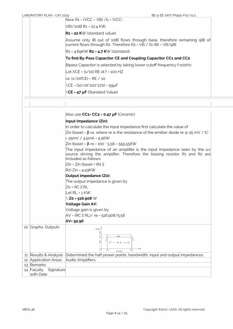
10 Graphs, Outputs
11 Results & Analysis Determined the half power points, bandwidth, input and output impedances.12 Application Areas Audio Amplifiers.13 Remarks14 Faculty Signature
with Date
18EEL38 Copyright ©2017. cAAS. All rights reserved.Page # 14 / 29
LABORATORY PLAN - CAY 2019 BE-5-EE-SKIT-Ph5b1-F02-V2.2
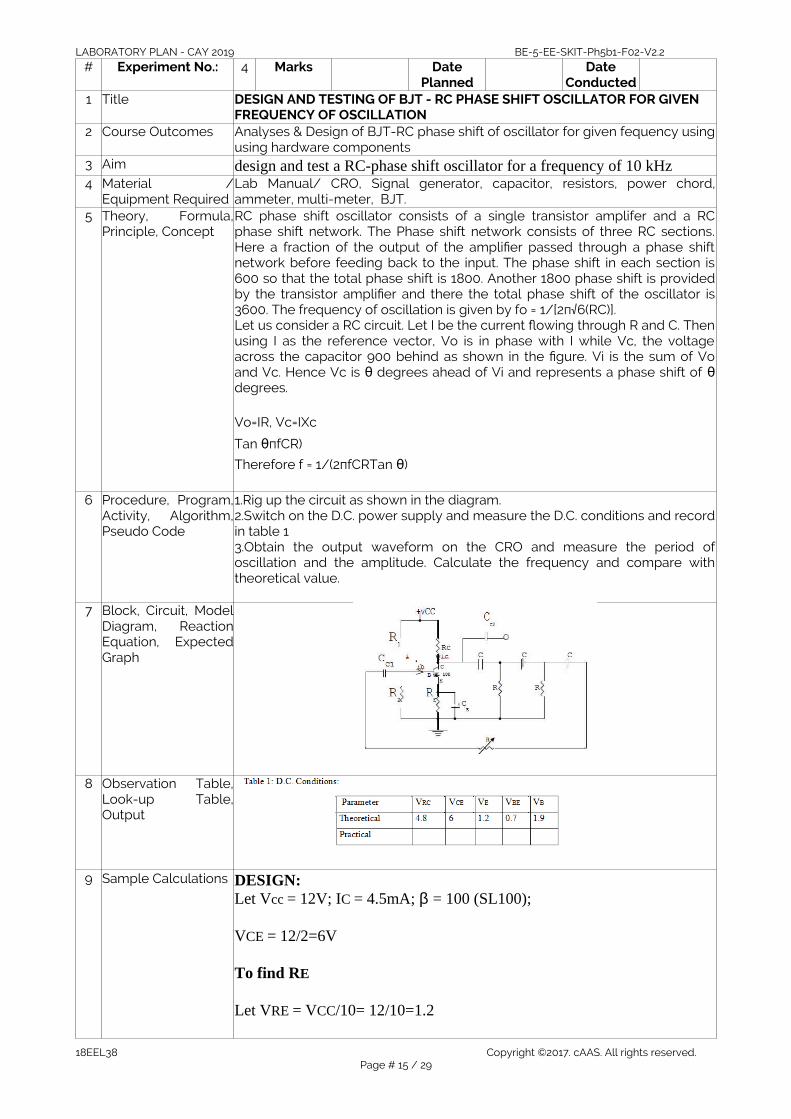
# Experiment No.: 4 Marks DatePlanned
DateConducted
1 Title DESIGN AND TESTING OF BJT - RC PHASE SHIFT OSCILLATOR FOR GIVENFREQUENCY OF OSCILLATION
2 Course Outcomes Analyses & Design of BJT-RC phase shift of oscillator for given fequency usingusing hardware components
3 Aim design and test a RC-phase shift oscillator for a frequency of 10 kHz 4 Material /
Equipment RequiredLab Manual/ CRO, Signal generator, capacitor, resistors, power chord,ammeter, multi-meter, BJT.
5 Theory, Formula,Principle, Concept
RC phase shift oscillator consists of a single transistor amplifer and a RCphase shift network. The Phase shift network consists of three RC sections.Here a fraction of the output of the amplifier passed through a phase shiftnetwork before feeding back to the input. The phase shift in each section is600 so that the total phase shift is 1800. Another 1800 phase shift is providedby the transistor amplifier and there the total phase shift of the oscillator is3600. The frequency of oscillation is given by fo = 1/[2п√6(RC)].Let us consider a RC circuit. Let I be the current flowing through R and C. Thenusing I as the reference vector, Vo is in phase with I while Vc, the voltageacross the capacitor 900 behind as shown in the figure. Vi is the sum of Voand Vc. Hence Vc is degrees ahead of Vi and represents a phase shift of θ degrees ahead of Vi and represents a phase shift of θ θ degrees ahead of Vi and represents a phase shift of θdegrees.
Vo=IR, Vc=IXc
Tan пfCR)θ degrees ahead of Vi and represents a phase shift of θ
Therefore f = 1/(2пfCRTan )θ degrees ahead of Vi and represents a phase shift of θ
6 Procedure, Program,Activity, Algorithm,Pseudo Code
1.Rig up the circuit as shown in the diagram.2.Switch on the D.C. power supply and measure the D.C. conditions and recordin table 13.Obtain the output waveform on the CRO and measure the period ofoscillation and the amplitude. Calculate the frequency and compare withtheoretical value.
7 Block, Circuit, ModelDiagram, ReactionEquation, ExpectedGraph
8 Observation Table,Look-up Table,Output
9 Sample Calculations DESIGN:Let Vcc = 12V; IC = 4.5mA; β = 100 (SL100);SL100);
VCE = 12/2=6V
To find RE
Let VRE = VCC/10= 12/10=1.2
18EEL38 Copyright ©2017. cAAS. All rights reserved.Page # 15 / 29
LABORATORY PLAN - CAY 2019 BE-5-EE-SKIT-Ph5b1-F02-V2.2
Therefore RE = VRE/IE ≈ VRE/IC
= 1.2/4.5Ma =267Ω (SL100);270 Ω std)
To find RC
From the Collector-Emitter loop writing KVL we getVCC- ICRC -VCE –VRE = 0
\ RC = (SL100);VCC – VCE – VRE) / IC
=(SL100);12-6-1.2)/4.5mA=1.07KW (SL100);1KW std)
10 Graphs, Outputs
11 Results & Analysis for (Theoritical) = 2kHz.for (practical ) = ----- kHz.
12 Application Areas13 Remarks14 Faculty Signature
with Date
18EEL38 Copyright ©2017. cAAS. All rights reserved.Page # 16 / 29
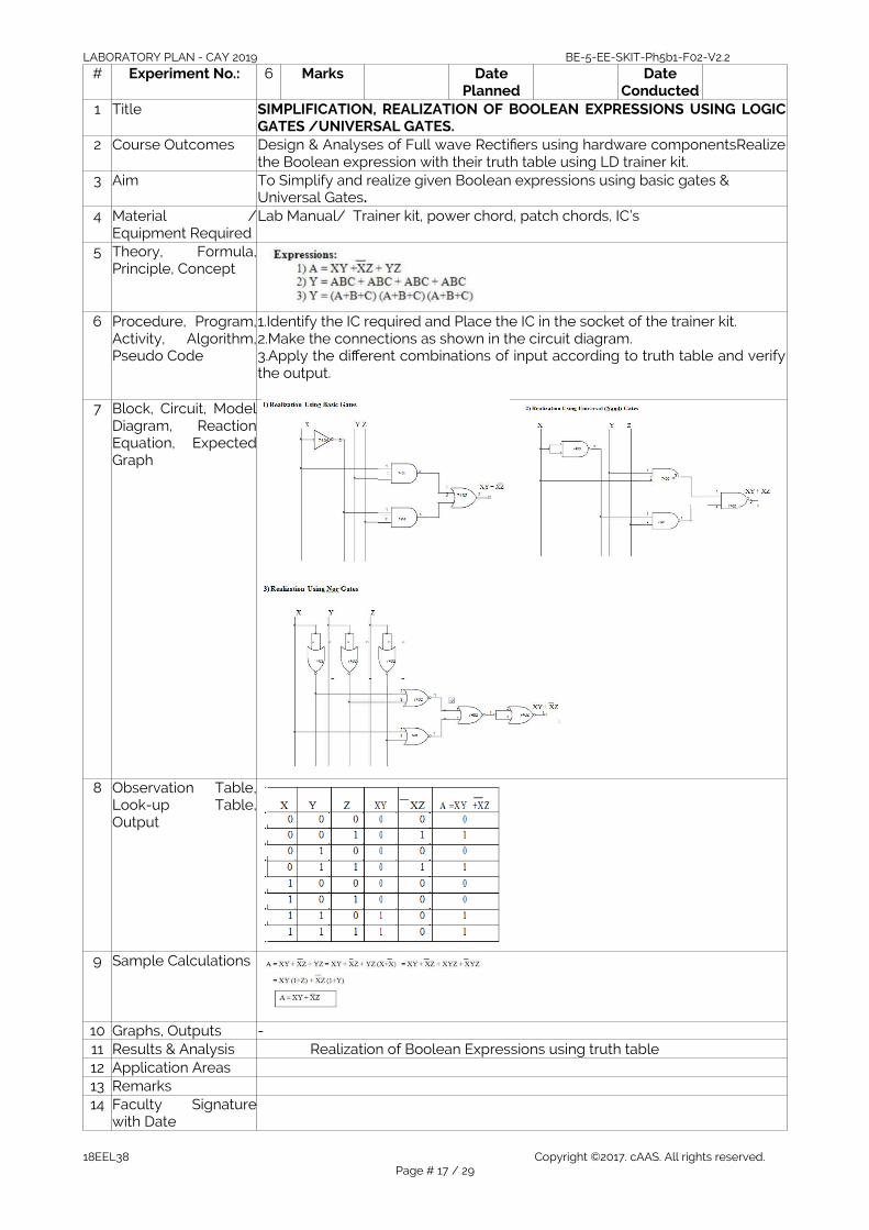
LABORATORY PLAN - CAY 2019 BE-5-EE-SKIT-Ph5b1-F02-V2.2
# Experiment No.: 6 Marks DatePlanned
DateConducted
1 Title SIMPLIFICATION, REALIZATION OF BOOLEAN EXPRESSIONS USING LOGICGATES /UNIVERSAL GATES.
2 Course Outcomes Design & Analyses of Full wave Rectifiers using hardware componentsRealizethe Boolean expression with their truth table using LD trainer kit.
3 Aim To Simplify and realize given Boolean expressions using basic gates & Universal Gates.
4 Material /Equipment Required
Lab Manual/ Trainer kit, power chord, patch chords, IC’s
5 Theory, Formula,Principle, Concept
6 Procedure, Program,Activity, Algorithm,Pseudo Code
1.Identify the IC required and Place the IC in the socket of the trainer kit.2.Make the connections as shown in the circuit diagram.3.Apply the different combinations of input according to truth table and verifythe output.
7 Block, Circuit, ModelDiagram, ReactionEquation, ExpectedGraph
8 Observation Table,Look-up Table,Output
9 Sample Calculations
10 Graphs, Outputs -11 Results & Analysis Realization of Boolean Expressions using truth table12 Application Areas13 Remarks14 Faculty Signature
with Date
18EEL38 Copyright ©2017. cAAS. All rights reserved.Page # 17 / 29

LABORATORY PLAN - CAY 2019 BE-5-EE-SKIT-Ph5b1-F02-V2.2
18EEL38 Copyright ©2017. cAAS. All rights reserved.Page # 18 / 29

LABORATORY PLAN - CAY 2019 BE-5-EE-SKIT-Ph5b1-F02-V2.2
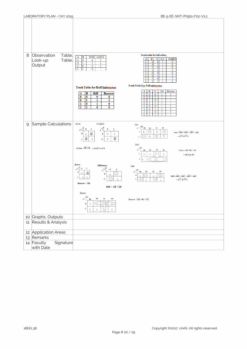
# Experiment No.: 7 Marks DatePlanned
DateConducted
1 Title REALIZATION OF HALF/ FULL ADDER AND HALF/ FULL SUBTRACTORUSING LOGIC GATES /UNIVERSAL GATES
2 Course Outcomes Realize the Adders & Substractors with their truth table using LD trainer kit.3 Aim To realize half/ full adder and substractor using logic gates /universal gates. 4 Material /
Equipment RequiredLab Manual/ Trainer kit, power chord, patch chords, IC’s
5 Theory, Formula,Principle, Concept
Half Adder and Full Adder Circuit. An adder is a digital circuit that performsaddition of numbers. The half adder adds two binary digits called as augendand addend and produces two outputs as sum and carry; XOR is applied toboth inputs to produce sum and AND gate is applied to both inputs toproduce carry.
The full subtractor is a combinational circuit which is used to performsubtraction of three input bits: the minuend , subtrahend , and borrow in . Thefullsubtractor generates two output bits: the difference and borrow out.
6 Procedure, Program,Activity, Algorithm,Pseudo Code
1.Identify the IC required and Place the IC in the socket of the trainer kit.2.Make the connections as shown in the circuit diagram.3.Apply the different combinations of input according to truth table and verify the output.
7 Block, Circuit, ModelDiagram, ReactionEquation, ExpectedGraph
18EEL38 Copyright ©2017. cAAS. All rights reserved.Page # 19 / 29
LABORATORY PLAN - CAY 2019 BE-5-EE-SKIT-Ph5b1-F02-V2.2
8 Observation Table,Look-up Table,Output
9 Sample Calculations
10 Graphs, Outputs11 Results & Analysis
12 Application Areas13 Remarks14 Faculty Signature
with Date
18EEL38 Copyright ©2017. cAAS. All rights reserved.Page # 20 / 29

LABORATORY PLAN - CAY 2019 BE-5-EE-SKIT-Ph5b1-F02-V2.2
# Experiment No.: 8 Marks DatePlanned
DateConducted
1 Title Realization of parallel adder/Sub tractors using 7483 chip- BCDto Excess-3 code conversion and Vice - Versa.
2 Course Outcomes Realize the parallel adder/Sub tractors and BCD to Excess-3 code conversionwith their truth table using LD trainer kit.
3 Aim To Realize a) Parallel Adder / subtractor using 7483.b) BCD to EXCESS – 3 code conversion and vice versa using 7483
4 Material /Equipment Required
Lab Manual/ Trainer kit, power chord, patch chords, IC’s
5 Theory, Formula,Principle, Concept
6 Procedure, Program,Activity, Algorithm,Pseudo Code
1.Make the connections as shown in the fig2.For Addition make Cin=0 and apply 4 bits of i/p for A and apply another setof 4 bit to B. Observe the O/P at S3 S2 S1 S0 and Carry generated at Cout.Repeat the steps for different inputs and tabulate the results.3.For Subtraction, Cin=1(A-B). By XOR-ing the i/p bits of B by 1, 1’s complementof B is obtained.4.Verify the the difference at S0,S1,S2,S3 and Cout. If Cout is 0, difference is_ve and difference is in 2’s Complement form. If Cout is 1, difference is +ve.5.Repeat the above steps for different inputs and tabulate the result.
7 Block, Circuit, ModelDiagram, ReactionEquation, ExpectedGraph
8 Observation Table,Look-up Table,Output
9 Sample Calculations
18EEL38 Copyright ©2017. cAAS. All rights reserved.Page # 21 / 29
LABORATORY PLAN - CAY 2019 BE-5-EE-SKIT-Ph5b1-F02-V2.2
10 Graphs, Outputs -11 Results & Analysis
12 Application Areas13 Remarks14 Faculty Signature
with Date
18EEL38 Copyright ©2017. cAAS. All rights reserved.Page # 22 / 29
LABORATORY PLAN - CAY 2019 BE-5-EE-SKIT-Ph5b1-F02-V2.2
# Experiment No.: 9 Marks DatePlanned
DateConducted
1 Title REALIZATION OF BINARY TO GRAY CODE CONVERTER AND VICE-VERSA2 Course Outcomes Realize the Binary to Gray code & vice versa using LD trainer kit.3 Aim To Realize Binary To Gray Code Conversion and Vice Versa 4 Material /
Equipment RequiredLab Manual/ Trainer kit, power chord, patch chords, IC’s
5 Theory, Formula,Principle, Concept
6 Procedure, Program,Activity, Algorithm,Pseudo Code
1.Identify the IC required and Place the IC in the socket of the trainer kit.2.Make the connections as shown in the circuit diagram.3.Apply the different combinations of input according to truth table and verify the output.
7 Block, Circuit, ModelDiagram, ReactionEquation, ExpectedGraph
8 Observation Table,Look-up Table,Output
9 Sample Calculations
18EEL38 Copyright ©2017. cAAS. All rights reserved.Page # 23 / 29

LABORATORY PLAN - CAY 2019 BE-5-EE-SKIT-Ph5b1-F02-V2.2
10 Graphs, Outputs -11 Results & Analysis
12 Application Areas13 Remarks14 Faculty Signature
with Date
18EEL38 Copyright ©2017. cAAS. All rights reserved.Page # 24 / 29
LABORATORY PLAN - CAY 2019 BE-5-EE-SKIT-Ph5b1-F02-V2.2
# Experiment No.: 10 Marks DatePlanned
DateConducted
1 Title DESIGN AND TESTING OF RING COUNTER/JOHNSON COUNTER2 Course Outcomes Design & Realize the Ring & Jogn counter using LD trainer kit. 3 Aim To wiring and testing Ring counter/Johnson counter 4 Material /
Equipment RequiredLab Manual/ Trainer kit, power chord, patch chords, IC 7495, 7404.
5 Theory, Formula,Principle, Concept
A ring counter is a type of counter composed of flip-flops connected into ashift register, with the output of the last flip-flop fed to the input of the first,making a "circular" or "ring" structure.There are two types of ring counters:A straight ring counter, also known as a one-hot counter, connects the outputof the last shift register to the first shift register input and circulates a singleone (or zero) bit around the ring.A twisted ring counter, also called switch-tail ring counter,walking ringcounter, Johnson counter, or Möbius counter, connects the complement ofthe output of the last shift register to the input of the first register andcirculates a stream of ones followed by zeros around the ring.A Johnson counter is a modified ring counter, where the inverted output fromthe last flip flop is connected to the input to the first. The register cyclesthrough a sequence of bit-patterns. The MOD of the Johnson counter is 2n if nflip-flops are used. The main advantage of the Johnson counter counter is thatit only needs half the number of flip-flops compared to the standard ringcounter for the same MOD.
6 Procedure, Program,Activity, Algorithm,Pseudo Code
1)Connections are made as per the circuit diagram of respective counter.2)Make the output of any flip-flop high using3)Disable PRT AND CLR of all flip-flops of counter.4)Keep applying the clock pulses, verify the truth table of respective counter.
7 Block, Circuit, ModelDiagram, ReactionEquation, ExpectedGraph
8 Observation Table,Look-up Table,Output
9 Sample Calculations -10 Graphs, Outputs -11 Results & Analysis
12 Application Areas13 Remarks14 Faculty Signature
with Date
18EEL38 Copyright ©2017. cAAS. All rights reserved.Page # 25 / 29
LABORATORY PLAN - CAY 2019 BE-5-EE-SKIT-Ph5b1-F02-V2.2
# Experiment No.: 11 Marks DatePlanned
DateConducted
1 Title DESIGN AND TESTING OF A SEQUENCE GENERATOR 2 Course Outcomes Design & Realize the Sequence generator using LD trainer kit. 3 Aim Design and testing a Sequence generator for the given sequence ………
1101011…….. 4 Material /
Equipment RequiredLab Manual/ Trainer kit, power chord, patch chords, IC’s
5 Theory, Formula,Principle, Concept
sequence generator is a digital logic circuit whose purpose is to produce aprescribed sequence of outputs. Each output will be one of a number ofsymbols or of binary or q-ary logic levels. Sequence generators are useful in awide variety of coding and control applications.
6 Procedure, Program,Activity, Algorithm,Pseudo Code
1.Mode control is made ‘1’2.Parallel data (SL100);say 0001) is applied to DCBA and a Clock pulse is applied sothat QDQCQBQA=00013.Now mode control is made zero and Clock pulse is applied such that‘one’ circulates around.
7 Block, Circuit, ModelDiagram, ReactionEquation, ExpectedGraph
8 Observation Table,Look-up Table,Output
9 Sample Calculations
10 Graphs, Outputs -11 Results & Analysis
12 Application Areas Sequence generators are useful in a wide variety of coding and controlapplications
13 Remarks14 Faculty Signature
with Date
18EEL38 Copyright ©2017. cAAS. All rights reserved.Page # 26 / 29
LABORATORY PLAN - CAY 2019 BE-5-EE-SKIT-Ph5b1-F02-V2.2
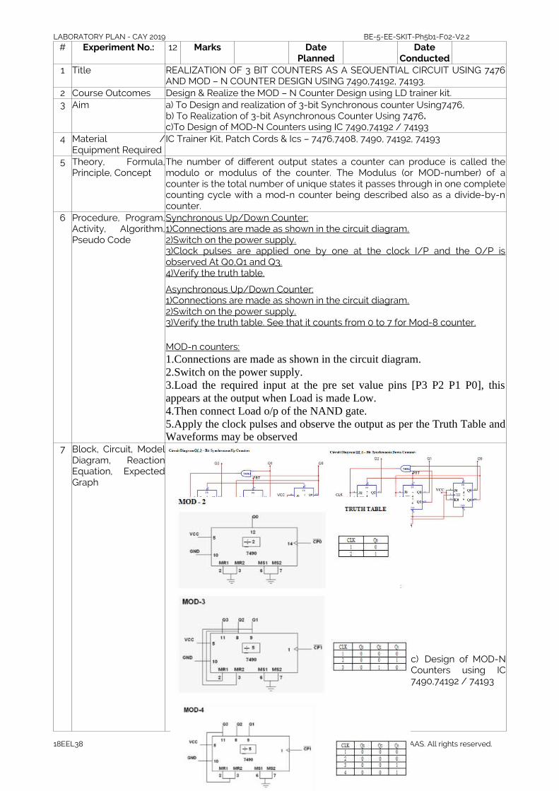
# Experiment No.: 12 Marks DatePlanned
DateConducted
1 Title REALIZATION OF 3 BIT COUNTERS AS A SEQUENTIAL CIRCUIT USING 7476AND MOD – N COUNTER DESIGN USING 7490,74192, 74193.
2 Course Outcomes Design & Realize the MOD – N Counter Design using LD trainer kit. 3 Aim a) To Design and realization of 3-bit Synchronous counter Using7476,
b) To Realization of 3-bit Asynchronous Counter Using 7476.c)To Design of MOD-N Counters using IC 7490,74192 / 74193
4 Material /Equipment Required
IC Trainer Kit, Patch Cords & Ics – 7476,7408, 7490, 74192, 74193
5 Theory, Formula,Principle, Concept
The number of different output states a counter can produce is called themodulo or modulus of the counter. The Modulus (or MOD-number) of acounter is the total number of unique states it passes through in one completecounting cycle with a mod-n counter being described also as a divide-by-ncounter.
6 Procedure, Program,Activity, Algorithm,Pseudo Code
Synchronous Up/Down Counter:1)Connections are made as shown in the circuit diagram.2)Switch on the power supply.3)Clock pulses are applied one by one at the clock I/P and the O/P isobserved At Q0,Q1 and Q3.4)Verify the truth table.
Asynchronous Up/Down Counter:1)Connections are made as shown in the circuit diagram.2)Switch on the power supply.3)Verify the truth table. See that it counts from 0 to 7 for Mod-8 counter.
MOD-n counters:1.Connections are made as shown in the circuit diagram.2.Switch on the power supply.3.Load the required input at the pre set value pins [P3 P2 P1 P0], thisappears at the output when Load is made Low.4.Then connect Load o/p of the NAND gate.5.Apply the clock pulses and observe the output as per the Truth Table andWaveforms may be observed
7 Block, Circuit, ModelDiagram, ReactionEquation, ExpectedGraph
c) Design of MOD-NCounters using IC7490,74192 / 74193
18EEL38 Copyright ©2017. cAAS. All rights reserved.Page # 27 / 29

LABORATORY PLAN - CAY 2019 BE-5-EE-SKIT-Ph5b1-F02-V2.2
8 Observation Table,Look-up Table,Output
MOD-8 Synchronous Up Counter
18EEL38 Copyright ©2017. cAAS. All rights reserved.Page # 28 / 29
LABORATORY PLAN - CAY 2019 BE-5-EE-SKIT-Ph5b1-F02-V2.2
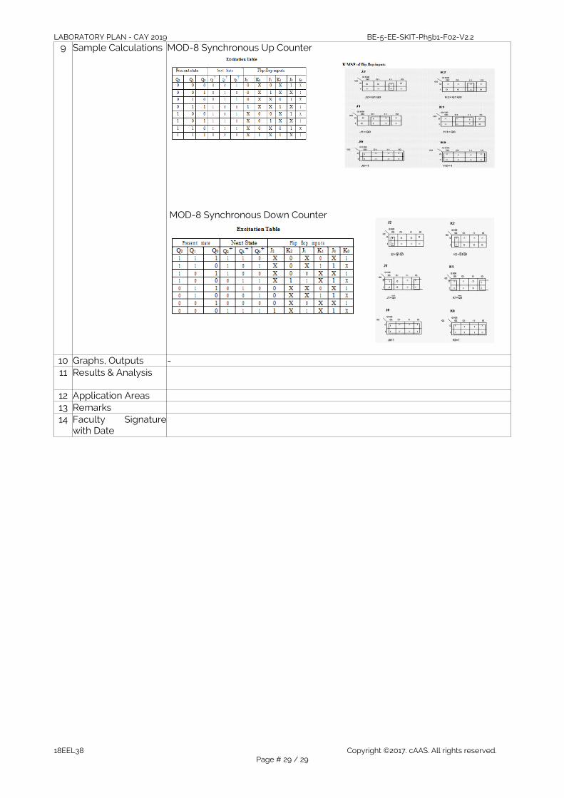
9 Sample Calculations MOD-8 Synchronous Up Counter
MOD-8 Synchronous Down Counter
10 Graphs, Outputs -11 Results & Analysis
12 Application Areas13 Remarks14 Faculty Signature
with Date
18EEL38 Copyright ©2017. cAAS. All rights reserved.Page # 29 / 29