spin-dependent transport in layered magnetic nanostructures
TRANSCRIPT
Charles University in Prague
Faculty of Mathematics and Physics
Doctoral Thesis
Spin-dependent transport in
layered magnetic nanostructures
Mgr. Karel Carva
Department of Condensed Matter Physics
Supervisor: Doc. RNDr. Ilja Turek, DrSc.
Prague, January 2007

Preface
During my PhD study I have learned a lot about its subject, the condensed matter theory,but also about other things which are no less valuable: I have seen the amenities anddifficulties of researcher’s work, understood the importance of team cooperation and theimportance of knowing where to find things someone else already revealed or developed.I also became familiar with writing scientific programs and utilizing the power of highperformance parallelized computers to carry out physical calculations using these programs.I have developed an extension of existing ab initio codes, which calculates lots of propertiesdescribed in this thesis and was therefore crucial for its accomplishment. The researchwhich ended in writing this thesis was done in cooperation with many other people, whoall I wish to thank here. I hope that that the results of this research presented here willcontribute to the main purpose of physics, the discovery of underlying laws of nature,namely to answering questions of condensed matter physics, and also offer methods thatmay help someone else to answer these questions too. In the future there is a big chancethat more practical applications based on ideas of the branch of physics presented here willbe brought to practice, which is something that assures us about the sense of our work.
First of all I would like to thank my supervisor Doc. RNDr. Ilja Turek, DrSc. forguiding me through the vast field of condensed matter theory, his advices were inevitablefor the success of my research work. For example he helped me to understand possibilitiesand limitations of ab initio calculations and the fact that despite the enormous extentof problems being within the reach of current computational condensed matter physicsrunning of programs is just a small portion of physicist’s work.
I am very grateful to Prof. RNDr. Vladimır Sechovsky, DrSc. for the support of allkinds that he provided to my research as well as the research of the whole department. Ithank to RNDr. Josef Kudrnovsky, CSc. for motivating discussions that provided me withinformation about current research topics and helped me to find some astonishing thingsin physics and also in physicist’s life.
I would like to express my thanks to my girlfriend Petra Bernatzikova for supporting meand withstanding my complete lack of free time during the work on this thesis. I would liketo thank to my colleague RNDr. Jan Rusz, Ph.D., with whom I had many inspirative talksand could share experience with many various topics and problems encountered during thetime of my studies. I thank to Dr. Olivier Bengone, Ph.D. who showed me many interestingpoints of view on studied topics and also developed the initial part of transport extensionto electronic structure code.
I thank to Doc. RNDr. Radomır Kuzel, CSc., who was always very supportive andshowed true interest in good operation of the department. I am grateful to Doc. RNDr.
1
2
Martin Divis, CSc. and Prof. RNDr. Bedrich Velicky, CSc. for all valuable knowledgethey supplied me during my studies. I thank to Doc. RNDr. Pavel Svoboda, CSc. andDoc. RNDr. Ladislav Havela, CSc. for acquainting me with interesting topics in physicsdifferent from my subject of study.
I thank to my colleagues RNDr. Jana Poltierova-Vejpravova, RNDr. Standa Danis,Ph.D., RNDr. Jirı Prchal, Ph.D., Mgr. Jirı Pospısil, RNDr. Jan Prokleska, Mgr. KlaraUhlırova and Mgr. Zdenek Matej, who made the atmosphere on the department veryfriendly and informal, made me understand many things and were always very helpfulwhen they help was needed. Last but not least I would like to thank to my parents, whowere always standing by me.
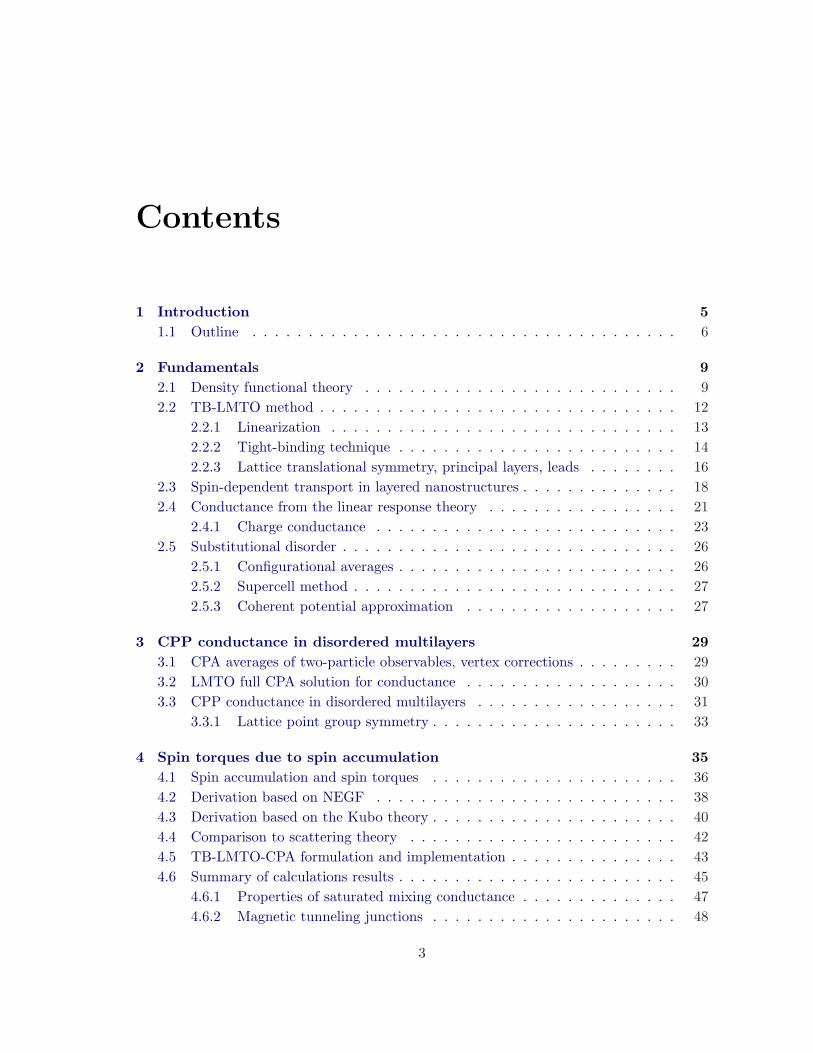
Contents
1 Introduction 51.1 Outline . . . . . . . . . . . . . . . . . . . . . . . . . . . . . . . . . . . . . . 6
2 Fundamentals 92.1 Density functional theory . . . . . . . . . . . . . . . . . . . . . . . . . . . . 92.2 TB-LMTO method . . . . . . . . . . . . . . . . . . . . . . . . . . . . . . . . 12
2.2.1 Linearization . . . . . . . . . . . . . . . . . . . . . . . . . . . . . . . 132.2.2 Tight-binding technique . . . . . . . . . . . . . . . . . . . . . . . . . 142.2.3 Lattice translational symmetry, principal layers, leads . . . . . . . . 16
2.3 Spin-dependent transport in layered nanostructures . . . . . . . . . . . . . . 182.4 Conductance from the linear response theory . . . . . . . . . . . . . . . . . 21
2.4.1 Charge conductance . . . . . . . . . . . . . . . . . . . . . . . . . . . 232.5 Substitutional disorder . . . . . . . . . . . . . . . . . . . . . . . . . . . . . . 26
2.5.1 Configurational averages . . . . . . . . . . . . . . . . . . . . . . . . . 262.5.2 Supercell method . . . . . . . . . . . . . . . . . . . . . . . . . . . . . 272.5.3 Coherent potential approximation . . . . . . . . . . . . . . . . . . . 27
3 CPP conductance in disordered multilayers 293.1 CPA averages of two-particle observables, vertex corrections . . . . . . . . . 293.2 LMTO full CPA solution for conductance . . . . . . . . . . . . . . . . . . . 303.3 CPP conductance in disordered multilayers . . . . . . . . . . . . . . . . . . 31
3.3.1 Lattice point group symmetry . . . . . . . . . . . . . . . . . . . . . . 33
4 Spin torques due to spin accumulation 354.1 Spin accumulation and spin torques . . . . . . . . . . . . . . . . . . . . . . 364.2 Derivation based on NEGF . . . . . . . . . . . . . . . . . . . . . . . . . . . 384.3 Derivation based on the Kubo theory . . . . . . . . . . . . . . . . . . . . . . 404.4 Comparison to scattering theory . . . . . . . . . . . . . . . . . . . . . . . . 424.5 TB-LMTO-CPA formulation and implementation . . . . . . . . . . . . . . . 434.6 Summary of calculations results . . . . . . . . . . . . . . . . . . . . . . . . . 45
4.6.1 Properties of saturated mixing conductance . . . . . . . . . . . . . . 474.6.2 Magnetic tunneling junctions . . . . . . . . . . . . . . . . . . . . . . 48
3
4 CONTENTS
5 Spin torques in non-collinear layered systems 515.1 Spin currents and spin-transfer torques . . . . . . . . . . . . . . . . . . . . . 515.2 Ab initio formulation . . . . . . . . . . . . . . . . . . . . . . . . . . . . . . . 54
5.2.1 Spin currents from linear response theory . . . . . . . . . . . . . . . 545.2.2 TB-LMTO expression . . . . . . . . . . . . . . . . . . . . . . . . . . 555.2.3 Ab initio torkance in non-collinear spin valves . . . . . . . . . . . . . 57
5.3 Comparison to spin-mixing conductance . . . . . . . . . . . . . . . . . . . . 585.4 Summary of calculations results . . . . . . . . . . . . . . . . . . . . . . . . . 61
5.4.1 Angular dependence . . . . . . . . . . . . . . . . . . . . . . . . . . . 63
6 Co/Cu multilayers with substitutional disorder 676.1 Electronic structure . . . . . . . . . . . . . . . . . . . . . . . . . . . . . . . 676.2 Co | Cu | Co multilayers with interface roughness . . . . . . . . . . . . . . . 68
6.2.1 Transport properties . . . . . . . . . . . . . . . . . . . . . . . . . . . 696.2.2 Comparison to supercell calculations . . . . . . . . . . . . . . . . . . 70
6.3 Co | Cu0.84Ni0.16 | Co trilayers with randomness in the spacer . . . . . . . . 716.4 CoCr | Cu | Co trilayers exhibiting negative GMR . . . . . . . . . . . . . . 72
6.4.1 Transport properties . . . . . . . . . . . . . . . . . . . . . . . . . . . 726.4.2 The origin of the negative GMR . . . . . . . . . . . . . . . . . . . . 736.4.3 The influence of interface interdiffusion . . . . . . . . . . . . . . . . 75
7 (Ga,Mn)As thin layers 777.1 Bulk (Ga,Mn)As . . . . . . . . . . . . . . . . . . . . . . . . . . . . . . . . . 78
7.1.1 Lattice defects . . . . . . . . . . . . . . . . . . . . . . . . . . . . . . 797.1.2 Uncompensated DLM state . . . . . . . . . . . . . . . . . . . . . . . 84
7.2 Ideal (Ga,Mn)As layers coupled to metallic leads . . . . . . . . . . . . . . . 847.3 (Ga,Mn)As layers with lattice defects . . . . . . . . . . . . . . . . . . . . . . 89
7.3.1 Uncompensated DLM state . . . . . . . . . . . . . . . . . . . . . . . 91
8 Co2MnSi thin layers 958.1 Bulk properties . . . . . . . . . . . . . . . . . . . . . . . . . . . . . . . . . . 958.2 Thin layers . . . . . . . . . . . . . . . . . . . . . . . . . . . . . . . . . . . . 988.3 Spin valves . . . . . . . . . . . . . . . . . . . . . . . . . . . . . . . . . . . . 101
9 Conclusions 103
A Kubo formula for generalized CPP transport 105
B Invariance property of spin-mixing conductance 109
Bibliography 113
Chapter 1
Introduction
Interaction between magnetic and electric properties is a phenomenon that attracts a lotof attention of physicists and also engineers, spin-dependence of electron transport is animportant subject of research. Consider the fact that magnetism allows information tobe permanently stored while electron transport allows its distribution. Both of them cancooperate in its analysis. Magnetoresistance is a change of resistance under influence ofa magnetic field, hence it allows for a detection of a magnetic state. It was discovered in1856 by Lord Kelvin and originates from the Lorentz force acting on the itinerant electrons,which causes extra deflection on their trajectories. This kind of magnetoresistance in bulkmaterials reaches very low values of up to a few percent. It depends on the angle betweencurrent direction and the orientation of magnetization, hence it is called anisotropic mag-netoresistance (AMR). Bulk magnetoresistance can go up to much higher values for somerecently found materials, typically f-electron based, where the jump in resistance can beattributed to a magnetism induced phase transition, but these phenomena happen usuallyat uselessly low temperatures and require high switching fields.
A completely different source of magnetoresistance arises on microscopic scale, fromthe spin-dependence of electron scattering at interfaces. The transition probability of spin-polarized electrons is strongly influenced by the spin-polarization of states in the magneticmaterial it is entering. In order to exploit this effect, the distances between spin-polarizedinterfaces must be smaller than the spin diffusion length, so that electrons incident onan interface remain polarized from the previous one. With the advent of new fabricationtechniques, such as molecular beam epitaxy (MBE) it became possible to manufacturethese nanoscale systems. Only one dimension is required to fulfill that size condition,which is the case of thin layers or its many repetitions to amplify the effect: multilayers.Another important point was the observation of the interlayer exchange coupling (IEC)in 1986 [1], that may cause antiparallel orientation of the mentioned thin magnetic layersin the ground state and allows lower magnetization switching fields than in setups withnegligible IEC. These progresses stimulated the discovery of the giant magnetoresistance(GMR) [2] and the tunneling magnetoresistance (TMR) [3], which capitalize the idea ofmultiple spin-dependent electron scattering at interfaces, their principle is explained inchapter 2.3. The corresponding magnetoresistance ratio (according to the definition inEq. 2.37) reaches values of up to a few hundred percent, note for example the MR ratioof 271% found in a Co | MgO | Fe junction at room temperature [4]. Recently also other
5
6 CHAPTER 1. INTRODUCTION
different microscopic processes were found to give rise to high magnetoresistance. Tunnelinganisotropic magnetoresistance (TAMR) was shown to reach values of the same order in(Ga,Mn)As based diluted semiconductors [5, 6]. This effect is believed to be caused not bythe spin-dependent interface scattering, but by the spin-orbit coupling. It is also presentonly in thin layers, where the necessary additional symmetry breaking can be achieved.
The GMR effect was recognized to be so interesting for the industry that it took onlyabout a decade since its discovery until it was applied in consumer electronic devices [7].This success has stimulated higher interest in spin-dependent transport and that branch ofphysics has later shown itself to be extraordinary fruitful. Devices combining intentionallyeffects of spin and electronics have been proposed and this whole topic has been coveredin under the name spintronics. Magnetoresistance represents not only reading, but alsofurther operations on signal. This is the case of recently proposed spintronics device: aspin valve transistor [8]. It is basically a combination of the GMR effect and semiconductortransistor technology. In addition to traditional metal base transistors it features a baseincluding two FM layers with different coercivities leading to spin-dependent scattering ofhot electrons. As for GMR the spin-dependent scattering of electrons depend on the relativeorientations of the two layers, which can be controlled due to their different coercivities. Theratio between collector and emitor current is much higher than the CIP-magnetoresistanceof this system, which is explained by much higher sensitivity of hot electrons to its meanfree path and subsequent exponential dependence of collector current on it. Spin valvetransistors are not examined here, but represent an example of the vast opportunities ofcombining spin and semiconductor technology.
The magnetization influences strongly the electron transport. As was pointed out bySlonczewski [9], an opposite effect is also possible: Spin polarized current incident on a dif-ferently polarized FM layer exerts a spin torque which rotates the magnetization directionof that FM layer. Spin polarization of the current can be achieved in another FM layerpreceding the rotated one. This effect has no relation to Oersted fields and can be easilyrecognized from it by its behavior with respect to current direction reversal. It has alsoan important advantage over magnetic field induced switching, where the switching fieldis roughly independent of grain size. The magnetic field due to current decreases with de-creasing wire radius at constant current density. The spin torque effect allows applications,which avoid direct manipulation with magnetic field and its source and it scales differently:It is independent of wire radius at constant current density, therefore it dominates overOersted fields caused by the same current for low wire radii, typically the threshold radiusis about 0.1µm [10, 11]. One of the applications can be a nonvolatile magnetic computermemory (MRAM) with top parameters comparable to classical computer random accessmemory (DRAM) and without a need for constant power supply. If the spin torque isinsufficient to rotate magnetization to another stable position, the magnetization precess,which gives rise to radio frequency oscillations on nanoscale [12, 13]. This is a convenientlymeasurable effect and another prospect for interesting applications.
1.1 Outline
The main aim of this work is to develop and apply first principles (ab initio) methodsto deal with the presented phenomena. Chapter 2 describes ab initio methods and other
1.1. OUTLINE 7
fundamentals necessary to understand the physics employed in subsequent text. Chapters 3-5 present novel methods developed in this work and together with Chapter 2 they constitutethe theoretical part of this thesis.
Existing theoretical results for transport in thin layers based on the local spin den-sity approximation (LSDA, Sec. 2.1), linear muffin-tin orbital (LMTO, Sec. 2.2) methodand Kubo-Landauer formalism (Sec. 2.4.1) are in many cases in good agreement with ex-periments. Significant problems arise for systems with substitutional disorder, either atinterfaces or spread across thin layers. These problems have been up to now solved bymeans of the supercell method (Sec. 2.5.2), where the results are quite satisfactory, but itscalculations’ numerical demands can grow very fast and there are some other drawbacks.An alternative approach is based on the coherent potential approximation (CPA - Sec.2.5.3), and its first complete application to transport in 2D structures without crude ap-proximations neglecting the effect of two-particle correlated motion is described in Chapter3 (already published in [14]).
Many works have been published about the dynamics of system under influence of agiven spin torque, but quantitative understanding of this observable is no less necessary andthere are only plenty of publications dealing with ab initio evaluation of this phenomena[15]. Chapters 4 and 5 of this work attempt to contribute solving questions related to thistopic. More approaches are available: One can see spin torques as results of an influenceof infinitesimally small spin accumulation (Sec. 4.2) in NM lead adjacent to the FM layeras described in Chapter 4 and soon to be published [16]; or it is possible to describe thewhole non-collinear spin valve and evaluate the spin torque acting on one of FM layers,which is done in chapter 5. The first approach gives more insight into the mechanism ofcurrent induced magnetization reversal and the role of material properties, while the secondone corresponds better to real experiments and catches properties connected with the non-collinear setup as is the angular dependence of calculated quantities. The correspondenceof these two approaches was also studied (Sec. 5.3). Both these chapters contain a sectionsummarizing main results obtained for real materials, more details about these materialscan be found in the second part of this thesis.
All transport calculations presented in this work assume linear response regime, whichallows to utilize the successful Kubo theory (Sec. 2.4) [17, 18]. Some derivations shownhere (Sec. 4.2) are based on non-equilibrium Green’s function formalism [19], but they areconfined to zero bias. Non-equilibrium situations with finite bias represent a formidableproblem beyond the scope of this work. Although there are many successful finite biascalculations [20, 21], some issues connected with lead self-energies [22, 23] or with the useof the DFT (discussed in Sec. 2.1) remain still unresolved. We have also proven that thepresented transport calculations are independent of the choice of partitioning of the systeminto the left and right lead and the intermediate region (provided that the preconditionsfor this partitioning are satisfied), see Appendix B.
The second part of this thesis demonstrates applications of the derived theories andmethods for various particular systems. In Chapter 6 Co|Cu|Co based trilayers are ex-amined with a special attention to the problem of interface interdiffusion. The cases ofmagnetic impurities in one Cu layer and other metal impurities in Co layers are also men-tioned. The latter case may lead to the negative GMR, this rather rare situation is explainedin Sec. 6.4.2.
8 CHAPTER 1. INTRODUCTION
Spintronics applications depend strongly on spin and hence it would be beneficial tohave a material which permits electrons with spin in only one direction, an ideal spin-filter.This requirement is satisfied by magnetic materials which behave partially like metals andpartially like semiconductors: half-metals [24], whose bands are spin-split in such a way,that the band crosses the Fermi energy in one spin direction while in the other one a bandgap is located at the Fermi energy (see Fig. 7.2 for an example density of states). Materi-als presented in Chapters 7, 8 are both half-metals. Chapter 7 describes diluted magneticsemiconductors (DMS) [25], a novel material combining properties of semiconductors withferromagnetism. They may also help to resolve the problem of spin injection into semi-conductors [26]. Their unique features are achieved by substituting some of atoms on itscation sublattice by magnetic impurities, a process which was made possible only recentlydue to the progress in technology. We examine its transport properties, the role of na-tive structural defects and also the spin-mixing conductance (Chap. 4), for which someunexpected findings are shown. Chapter 8 deals with a Heusler alloy Co2MnSi. Here thehalfmetallicity is accompanied by a very high Curie temperature. Its structure is simplerthan that of (Ga,Mn)As because in its ideal form it contains no intrinsic disorder, howeverwe find that disorder is probably present anyway in real samples in quite high amount asa defect and that it can explain some of experimental observations.
Chapter 2
Fundamentals
Most of the properties of the solids are closely related to the behavior of electrons, the par-ticles that holds atoms together to form a solid. The determination of electronic structure(ES) is thus a key step in realistic predictions of these properties, including the main subjectof this work: transport properties. Traditional ES calculations involving phenomenologicalparameters were given a more powerful alternative: The exponential rise of speed of avail-able computers made it possible to calculate the electronic structure from first principlesof quantum mechanics, thus avoiding any such parameters. They allow to describe widenumber of systems on equal footing, gain a better understanding of unexplained phenom-ena, test proposed theories rapidly, and predict behavior of systems in new conditions, witharbitrary modifications. These features can be combined so that one can even design com-pletely new materials with desired properties based on ab initio calculations. Even thoughexact solutions of the Schrodinger equation for a solid are far beyond capabilities of anycomputer, there are approximations that make ab initio solutions possible while retaininga high accuracy. The present chapter describes mainly the more or less general methodsnecessary for a particular ab initio scheme used in this work.
Atomic Rydberg units will be used throughout the text, hence ~ = 2me = e2/2 = 1,where me denotes the electron mass. This defines all other involved units, the length unitis the Bohr radius a0 = ~2
me2 = 1 (≈ 5.29.10−11 m ) and the energy unit is 1 RydbergERyd = e2
2a0= 1(≈ 13.6 eV ).
2.1 Density functional theory
Early attempts to solve any systems bigger than a few atoms from first principles werestopped by the complexity of many-electron problems. The number of electrons in solidsprevents any exact solution and calls for reasonable approximations. In 1964 Hohenberg andKohn[27] introduced a theory which is nowadays used as a powerful tool to reduce the many-electron ground state problem to a single-electron equivalent. The essence of their formalismis a change-over from many-electron wave functions Ψ (r1, s1,r2, s2...rN , sN ), where ri andsi denote the space and spin coordinates of i-th particle, to one-electron (spinless) densities
9
10 CHAPTER 2. FUNDAMENTALS
defined as
n(r) =∫d3r1d
3r2...d3rN
∑s1,s2,..,sN
N∑
i=1
|Ψ(r1, s1, r2, s2, ...rN , sN )|2 δ (r− ri) , (2.1)
which gave it its name density functional theory (DFT). The first Hohenberg-Kohn theoremstates that the electronic density n(r) of the ground state uniquely determines the externalpotential Vext(r) up to a trivial additive constant, and all other quantities are then inprinciple functionals of the electronic density also. The second theorem provides a recipehow to find the ground state: The ground state energy corresponding to the given externalpotential Vext(r) can be found by minimizing the total energy functional with respect tochanges in the electron density n(r) while the number of particles is held fixed. The densityassociated to the minimum total energy is the ground state density.
Soon after the discovery of the DFT a strong tool for condensed matter calculationsbased on these two general theorems was introduced, the Kohn-Sham equations [28]. Theyprovide a direct transition from the many-electron Hamiltonian to a single-electron onewith a different potential, the Kohn-Sham potential VS (r). The Schrodinger equation isthen replaced by the Kohn-Sham equation:
(−∇2 + VS(r))Ψi(r) = εiΨi(r) , (2.2)
where Ψi (r) is a one-electron wave function and εi the corresponding energy eigenvalue.It is a sum of the original external potential, Hartree-like term and an exchange-
correlation potential which incorporates all the many-body effects of the original system.
VS(r) = Vext(r) +∫
n(r′)|r− r′|dx
′ +δExc[n(r)]δn(r)
(2.3)
DFT is in principle exact, but the important exchange-correlation functional is definedin such a way that does not allow us to evaluate it directly. In the end it is necessary tointroduce some approximations to it, their choice depends on the specific situation. Surpris-ingly, even the crudest approximation of the exchange-correlation functional, local densityapproximation (LDA) [28] or local spin density approximation (LSDA) [29] is sufficient formany situations. It is based on an assumption that the xc-energy per one electron of oursystem in the position r is the same function of the local density n(r), as if our systemwould be entirely homogeneous with the same density. Therefore the L(S)DA exchange-correlation functional is local function, this fact is crucial for the speed of calculations. Thexc-energy per one particle εxc(n(r)) is specified by parameterizations which were obtainedfrom exact calculations of the homogeneous electron gas. The parameterization of Vosko-Wilk-Nusair [30] is adopted in the presented calculations. L(S)DA becomes exact only inthe limit of slowly varying spatial density and is therefore suited well to treat electroniccharge clouds where the electron density varies by but a small fraction of itself over a deBroglie length of a characteristic electron. There is a systematic overbinding predicted byLDA particularly for the s-p bonded systems due to strong energy gradients in these direc-tional bonds. Nevertheless it describes well electronic structure of wide class of materials,many of transition metals and simpler materials, one must avoid i.e. strongly correlated
2.1. DENSITY FUNCTIONAL THEORY 11
systems, where LDA+U functional [31] or the dynamical mean-field theory [32] would beappropriate.
Since the whole problem is expressed as a set of integro-differential equations (2.2, 2.3)allowing no analytical solution, it must be solved iteratively. The direct iteration procedurediverges, hence a mixing with previous iterations must be used. Accelerated mixing schemebased on the Anderson mixing [33] was used in calculations presented here. More detailscan be found in Sec. 10.8.2 of [34].
Note that the key quantity in DFT, the density of states, is closely related to theresolvent of the Hamiltonian H, i.e. its Green’s function (GF) [31, 35]:
G (z) = (z −H)−1 =∫ ∞
−∞
1z − εδ (ε−H) dε , (2.4)
where z is a complex energy variable. Retarded and advanced Green’s functions are definedas Gr (E) = G (E − i0) and Ga (E) = G (E + i0), respectively, where symbol 0 denotes aninfinitesimally small value and its sign is important. One can quickly show thatGa = (Gr)+,the imaginary part operator is here commonly redefined so that it in fact provides itsantihermitean part: 2iImGr = Gr−Ga. An important property of Green’s functions is thefact that the spectral density δ (E −H) is directly related to its imaginary part:
δ (E −H) = − 1π
ImGr (E) . (2.5)
Then one knows also the way to obtain the total density of states defined as
N (E) = Tr δ (E −H) . (2.6)
The Green’s function may be expressed using the orthogonal and complete set of eigen-functions Ψi (r) and eigenenergies εi in the form:
G(r, r′, z
)=
∑
i
Ψi (r)Ψ∗i (r′)
z − εi . (2.7)
The local single-particle density n(r) is given by an energy integration of the spectral densityat point r multiplied by the Fermi-Dirac distribution f (E):
n (r) = − 1π
∫ ∞
0f (E) ImGr (r, r, E) dE . (2.8)
In this work calculations are restricted to zero temperature, hence f (E) = ϑ (E − EF ),where ϑ (E) denotes the Heavyside function. Since there are poles in the Green’s functionson the real axis at points corresponding to eigenvalues of the Hamiltonian, energy integra-tions over the occupied part of the valence bands are performed here in the complex energyplane along a closed contour starting and ending at the Fermi energy (Chap. 10.3 of [34]).For evaluation of Green’s functions near the real energy axis the analytic continuation isused (Chap. 10.4 of [34]).
A lot of discussion concerns the question if DFT as a ground state theory is suitablefor transport calculation. The presented work is restricted to the linear response regime,
12 CHAPTER 2. FUNDAMENTALS
one can then assume that the single particle potential of the ground state, obtained fromDFT, is not changed by the transported electrons. Note that there is a well-known problemwith DFT prediction of the band gap in insulating solids or semiconductors. The propertreatment of band gap or finite bias calculations, an excited state DFT extension like theGW approximation [31, 36] or time-dependent DFT [37–39], would be too computationallyexpensive, but within the linear response regime the corresponding error again should notbe significant. More likely the previously mentioned error due to exchange-correlationpotential is more important.
2.2 TB-LMTO method
When solving the one-electron Kohn-Sham equation (2.2), the basic point of ES calculationis a reasonable choice of an approximative description of potential and basis in Hilbert space.We adopt here muffin-tin potentials approximated as:
• spherically symmetric potential inside non-overlapping spheres centered on individualnuclei. The positions of its centers are labeled R. The potential can then be writtenas
V (r) = VR(rR) , rR ≤ sR , (2.9)
where VR(r) is the potential inside the R-th atomic sphere of radius sR (Wigner-Seitzradius), rR denotes the difference vector r−R and r the magnitude of vector r.
• constant potential in the interstitial area.
It is combined with the atomic sphere approximation (ASA) - spheres are slightly overlap-ping, kinetic energy in the interstitial region is neglected. This region is then described bythe Laplace equation. These are distinctive approximations in comparison to full potentialbased methods (with no approximation of the potential shape), but calculations based on itare much less computationally demanding and for a wide class of materials the introducederror is almost negligible. Furthermore full potential methods can hardly be combined withthe coherent potential approximation (sec. 2.5.3). The basis may then be constructed asfollows [34, 40]:
In the interstitial region the wave function satisfies the Laplace equation. Its solutionis expressed in terms of spherical harmonics YL (r) and radial amplitudes al (r), wherer = r/r is a unit vector parallel to r and index L stands for usual angular momentumindices (l, m). The differential equation for al (r) leads to the irregular solutions KL (r)and the regular solutions JL (r). The former one centered at R can be expanded in termsof the latter centered at R′ (R′ 6= R), which introduces the so called structure constantsSLRL′R′ describing the geometry of the problem:
KL (rR) =∑
L′SRLR′L′JL′ (rR′) . (2.10)
The solutions φRl (r, E)YL (r) of radial Schrodinger equation for a single isolated spherewith spherically symmetric potential and interstitial region solutions must be matched
2.2. TB-LMTO METHOD 13
smoothly (up to first derivative) on the sphere boundary given by the Wigner-Seitz ra-dius sR. This condition leads to the definition of the potential function PRl (E) and thenormalization function NRl (E):
PR`(E) =K`(r), ϕR`(r, E)J`(r), ϕR`(r, E) |r=sR , (2.11)
NR`(E) =w
21
ϕR`(r,E), J`(r) |r=sR , (2.12)
where f1(r), f2(r) is the Wronskian of two radial functions (Eq. 2.20 of [34]). Thesefunctions ensure correct matching of the two solutions:
NR`(E) ϕR`(r, E) → K`(r) − PR`(E) J`(r) . (2.13)
The so called muffin-tin orbitals are constructed in analogy to the partial waves in themultiple scattering theory [41, 42] from the solutions of the two regions:
ΨRL (r, E) = NRl (E)φRl (r, E) + PRl (E) JL (rR) for rR ≤ sR ,
= KL (rR) for rR ≥ sR . (2.14)
The parts of ΨRL(r, E) inside and outside the R-th sphere are often referred to as thehead and the tail of the muffin-tin orbital (2.14), respectively. For regions rR′ ≤ sR’ ofmuffin-tin orbitals (2.14) the expansion (2.10) is used. Linear combinations of such muffin-tin orbitals satisfy the Schrodinger equation (2.2) provided that the coefficients for JL (rR)inside each sphere are canceled by incoming tails (2.10) from other spheres. Non-trivialsolutions of this tail cancellation condition corresponds to the following equation:
det (PRL (E) δRLR′L′ − SRLR′L′) = 0 , (2.15)
where we defined the on-site canonical structure constants trivially such that
SRL,RL′ = 0 . (2.16)
Eq. (2.15) is often called the KKR-ASA secular equation for its close similarity with theKohn-Korringa-Rostoker (KKR) matrix derived within the multiple scattering formalism[41, 42]. More details of its derivation can be found in [34]. This equation clearly showsa separation of the problem into two parts: potential functions PRL (E) that describe theproperties of the individual atomic spheres and structure constants related to the posi-tions of the atomic spheres. The disadvantage lies in the non-linear energy dependence ofPRL (E), which will be removed in the next section.
2.2.1 Linearization
Let us recall that solving the Schrodinger equation (2.2) is equivalent to the use of thevariational procedure
δ
∫ψ(r) [−∆ + V (r) ] ψ(r) d3r = 0 ,
∫ψ2(r) d3r = 1 , (2.17)
14 CHAPTER 2. FUNDAMENTALS
where the second equation represents a normalization constraint. For simplicity, we use onlyreal wave functions ψ(r) in Eq. (2.17) which is consistent with the use of a real potentialV (r) in Eq. (2.2). Due to the constraint in Eq. (2.17), the energy E enters the variationalapproach as a Lagrange multiplier. If the trial wave function ψ(r) is assumed in the form ofa linear combination of basis functions χi(r) which satisfy the correct boundary conditions,the variational principle (2.17) leads to the following eigenvalue problem:
det (E Oij − Hij ) = 0 , (2.18)
where the Hamiltonian matrix Hij and the overlap matrix Oij are given by
Hij =∫
χi(r) [−∆ + V (r) ] χj(r) d3r ,
Oij =∫
χi(r) χj(r) d3r . (2.19)
Analogous procedure can be performed for the Schrodinger equation in ASA and allows fora reduction of the original problem (KKR-ASA secular equation) to an eigenvalue prob-lem, provided that the basis function χi (r) are energy independent. The basis can betransformed so that overlap matrix O is replaced by the unit matrix, and an orthogonalHamiltonian is obtained.
The linearization of the KKR-ASA secular equation corresponds to an approximationof radial amplitudes φRl (r, E) by its Taylor expansion in energy truncated after its firsttwo terms(thus linear). The potential function PRL (E) can be written as a fraction of twolinear functions, which is uniquely parameterized by three constants CR`, ∆R`, γR` calledpotential parameters. One possible parameterization of PRL (E) is given by
PR`(E) =E − CR`
∆R` + γR` (E − CR`). (2.20)
The exact and parameterized potential functions are required to coincide at the energyexpansion point Eν,Rl up to the second derivative. The KKR-ASA secular equation (2.15)expressed using the parameterization (2.20) can be reduced to a standard eigenvalue prob-lem of the type
det(E δRL,R’L′ − Horth
RL,R’L′)
= 0 , (2.21)
where the orthogonal Hamiltonian Horth corresponds to a new orthogonal basis of theso-called linearized muffin-tin orbitals.
2.2.2 Tight-binding technique
It is desirable to reduce Hamiltonians with a far reaching interaction between sites (inLMTO corresponding to slowly decaying structural constants) to rather limited ones withinteraction only between nearest neighbors. These are analogues of simple tight-bindingmodels, but with ab initio calculated parameters that best reproduce the true physics, i.e.give results closest to that of original Hamiltonian. Green’s functions (Sec. 2.1) representa fundamental tool in physical ab initio calculations and are crucial for accomplishing this
2.2. TB-LMTO METHOD 15
job. One of its biggest advantages is that it easily allows for perturbation expansion. Foran unperturbed Hamiltonian H = H0 + U an unperturbed Green’s function is defined:(z −H0
)G0 = 1. In ASA the unperturbed linear operator corresponds to the following
equation for the interstitial area:
z +H0(r, r′
)= ∆rδ
(r− r′
). (2.22)
The choice of the unperturbed part of potential is in principle arbitrary, and the tight-binding method is based on a different choice of potential (V1) that leads to the least extendof interaction. A transformation was found, that redefines the potential (expressed in termsof LMTO potential functions and screening constants) in such way, that Green’s functionscorresponding to that virtual potential can be easily calculated, and then transformed backto its physical counterpart.
The transformation to a representation with the limited interaction extent is thereforecalled the screening transformation (inspired by the electrostatic screening) and the cor-responding screened potential functions Pα
R`(z) and screened structure constants SαRL,R’L′
are defined by the following implicit equations:
PαR`(z) = PR`(z) + PR`(z)αR`P
αR`(z) ,
SαR’L′,R”L′′ = SR’L′,R”L′′ +
∑
RL
SR’L′,RLαR`SαRL,R”L′′ . (2.23)
In contrast to the vanishing on-site elements SRL,RL′ of the canonical structure constants,Eq. (2.16), the on-site elements Sα
RL,RL′ of the screened structure constants are generallynon-zero and reflect the environment of a particular site R (crystal field effects).
In LMTO it is customary to define an auxiliary Green’s function g (z) closely connectedto the original KKR-ASA secular equation (2.15):
g(z) = [ P (z) − S ]−1 , (2.24)
this object is more suitable for calculations. It is related to the physical Green’s functionby the formula
G(z) = λ(z) + µ(z)g(z) µ(z) , (2.25)
where diagonal matrices λ(z) and µ(z) can be expressed in terms of the potential function.The definitions of screened counterparts of these objects, non-diagonal matrix gα(z) anddiagonal matrices µα(z) and λα(z), are the same as of the unscreened ones, but related tothe screened potential function Pα(z). It is possible to find explicit expressions of Pα(z),µα(z) and λα(z) in terms of the second-order parameterization (2.20):
PαR`(z) =
z − CR`
∆R` + (γR` − αR`) (z − CR`),
µαR`(z) =
√∆R`
∆R` + (γR` − αR`) (z − CR`),
λαR`(z) =
γR` − αR`
∆R` + (γR` − αR`) (z − CR`). (2.26)
16 CHAPTER 2. FUNDAMENTALS
In agreement with the previous statements the physical Green’s function G(z) can beshown to be independent of the screening constant α. Note that structure constants ofthe unscreened system are closely related to unperturbed Green’s function of system withreference potential given by that chosen for interstitial area. Their screened counterpartsare related to unperturbed Green’s function of the “screening” reference potential V1. Thetransformation leading to the least extend of interaction will be denoted as β and thecorresponding optimal screening constants αRl = βl depend for a given lattice only on thecutoff value lmax.
The knowledge of the physical Green’s function allows one to calculate for examplethe density of states (Eq. 2.6). For the R-th atom it is given as (disregarding possiblesummation over spin states):
NR (E) = − 1π
∑
L
ImGrRL,RL (E) . (2.27)
2.2.3 Lattice translational symmetry, principal layers, leads
For systems with 3D translational symmetry the infinite problem of finding the auxiliaryGreen’s function is easily solvable by means of the lattice Fourier transformation. In thiscase, the lattice points R can be expressed in the form R = B + T, where the vectorsB denote the basis vectors (non-primitive translations), while the vectors T refer to thetranslation vectors (primitive translations). The translational invariance of the systemimplies the validity of the Bloch theorem and leads to the concepts of a reciprocal space,a reciprocal lattice, and Brillouin zones (BZ). The problem can then be transformed fromreal space to the reciprocal space, where it is diagonal and thus can be solved for eachvector k from the first BZ separately.
In systems with translational symmetry reduced to two dimensions (layered systems)the centers R of the space-filling atomic spheres can be written as R = B+T‖, where thevectors B specify in general individual atomic layers parallel to the interface (includingnon-trivial basis vectors in the presence of a long-range atomic order within the layers).The translation vectors T‖ are parallel to the interface and define a two-dimensional lat-tice in real space which in turn gives rise to the corresponding two-dimensional reciprocallattice. Translationally invariant two-center quantities XRL,R’L′ , i.e., matrices in RL suchas SRL,R’L′ satisfying
X(R+T‖)L,(R′+T‖)L′ = XRL,R’L′ , (2.28)
can be transformed into quantities XBL,B’L′(k‖) depending on vector k‖ from 2D BZ ac-cording to
XBL,B’L′(k‖) =∑
T‖
XBL,(B′+T‖)L′ exp(i k‖ ·T‖) . (2.29)
The inversion of this Fourier transformation (2.29) is usually called a BZ-integration andis traditionally written as
XBL,(B′+T‖)L′ =1
ABZ
∫
BZXBL,B’L′(k‖) exp(−i k‖ ·T‖) d2k‖
=1N‖
∑
k‖
XBL,B’L′(k‖) exp(−i k‖ ·T‖) , (2.30)
2.2. TB-LMTO METHOD 17
where ABZ denotes the area of the two-dimensional BZ andN‖ is related to two-dimensionalperiodic boundary conditions.
The direction perpendicular to interfaces is obviously excluded from this transformationand the dimension of the transformed matrices XBL,B′L′(k‖) remains infinite. In order todeal with this situation, the concept of principal layers is introduced. They are constructedfrom the original atomic layers in the following way: (i) each principal layer contains afinite number of neighboring atomic layers, (ii) the whole system can be considered as astacking of an infinite sequence of the principal layers labeled by an integer index p, and(iii) the elements Sβ
RL,R’L′ of the tight-binding structure constants are non-zero only forsites R and R’ belonging to the same or neighboring principal layers. The sites R of a givensystem can be then written in a form R ≡ (p,B,T‖) where p is the index of the principallayer, B denotes the corresponding basis vector (mostly atomic layer) in the p-th principallayer, and T‖ is a 2D translation vector. The tight-binding LMTO representation becomesparticularly useful in that situation as it reduces the minimum number ν of atomic layerscomprised in one principal layer. In the case of the most closely-packed planes, fcc(111)and bcc(110), the principal layer consists only of a single atomic layer, in other low-indexcases it is 2 or 3 layers (Tab. 3.4 of [34]) .
In practice the whole system is always truncated to a region of finite thickness, whichcan be calculated in finite time, the so called intermediate region. Outside this region thesystem is assumed to be already solved and described by a bulk-like electronic structure.It is desirable that the change of self-consistent electronic structure of boundary principallayers from its bulk counterpart is negligible, so that the two regions are smoothly matchedwithout creating any artificial interface. Therefore a sufficiently high number of layers ofthe same composition as the outer region must be included in the intermediate region. Notethat the role of contributions from truncated area to the intermediate region Hamiltonianis very important, without them the system would be just embedded in a vacuum withcompletely reflecting boundaries. For transport calculations the truncated part representsleads, which allow an influx and outflux of electrons to and out of the system. Results shouldnot depend on a particular choice of truncation positions inside the bulk-like regions, this isstudied in detail in Appendix B. These two semi-infinite parts of the system will be referredto as the left (L) and right (R) lead.
The Green’s function corresponding to the intermediate region Hamiltonian can thenbe found by means of the partitioning technique [43] for matrix inversions. We start with2D lattice Fourier transform of Eq. (2.24) and introduce the matrix
Mβ(k‖, z) = P β(z) − Sβ(k‖) , (2.31)
which describes the whole system and is used to calculate the auxiliary Green’s function:
Mβ(k‖, z) gβ(k‖, z) = 1 . (2.32)
The auxiliary Green’s function at layer p (omitting k‖- and z-dependences) is then givenas:
gβp,p =
P β
p − Sβp,p − Sβ
p,p−1
[(Mβ,p,<
)−1]p−1,p−1
Sβp−1,p
− Sβp,p+1
[(Mβ,p,>
)−1]p+1,p+1
Sβp+1,p
−1, (2.33)
18 CHAPTER 2. FUNDAMENTALS
where Mβ,p,<(k‖, z) and Mβ,p,>(k‖, z) are semi-infinite block submatrices of the matrixMβ(k‖, z) containing only layers p′, where p′ > p or p′ < p, respectively.
It motivates the definition of the surface Green’s functions [44, 45] for semi-infinitesystems, i.e. leads. Let us assume that the intermediate region comprises principal layersp, 1 ≤ p ≤ N . Layers pL (pL < 1) and pR (pR > N) then correspond to the left and rightlead, respectively. Let Mβ
L(k‖, z) denote the semi-infinite square submatrix for layers pL ofthe whole system matrix Mβ(k‖, z). The surface Green’s function (SGF) Gβ
L(k‖, z) of theconsidered semi-infinite stacking of principal layers is then defined as the (pL, pL) subblockof the inverted semi-infinite submatrix Mβ
L(k‖, z):
GβL(k‖, z) =
[MβL(k‖, z)
]−1
pL,pL, (2.34)
which is independent of the particular choice of pL due to the homogeneity of leads. Let usremind that this SGF is a matrix in BL-indices and that analogously a SGF Gβ
R(k‖, z) forthe right semi-infinite lead can be defined. Eq. (2.33) allows to evaluate auxiliary Green’sfunction in the intermediate region using only intermediate region properties and surfaceGreen’s functions for both leads. The formula for the intermediate region auxiliary Green’sfunction gβ
p,p′(k‖, z) can be recast into the form:
gβp,p′(k‖, z) = [ P β
p (z)δp,p′ − Sβp,p′(k‖)
−Σβ(k‖, z)]−1p,p′ , (2.35)
where
Σβ(k‖, z) = ΣβL(k‖, z) + Σβ
R(k‖, z) ,
ΣβL(k‖, z) = Sβ
1,0(k‖) GβL(k‖, z) S
β0,1(k‖) ,
ΣβR(k‖, z) = Sβ
N,N+1(k‖) GβR(k‖, z) S
βN+1,N (k‖) . (2.36)
The influence of leads is represented by these operators derived simply from SGF; they are infact self-energies representing the perturbation of the intermediate system due to presenceof leads [19]. Note that due to properties of principal layers they act only in the corners(1, 1) and (N,N) of the intermediate region subblock of the matrix M , in this text they areused as the matrix in layers space as well as its corner: Σβ
L p,p′(k‖, z) = ΣβL(k‖, z)δp,1δp′,1,
ΣβR p,p′(k‖, z) = Σβ
L(k‖, z)δp,Nδp′,N . Various methods of SGF evaluation can be found inSec. 10.6 of [34], here we use the renormalization-decimation technique [46], which is bestsuited for simulations with very low value of Im z. The screening transformation superscriptβ will be omitted in further text as all relevant quantities are assumed to be expressed inthe least-extend TB representation unless otherwise stated.
2.3 Spin-dependent transport in layered nanostructures
In systems with collinear magnetizations electrons spin direction must be also collinear toit, hence conductances of electrons restricted to spins parallel or antiparallel to the specified
2.3. SPIN-DEPENDENT TRANSPORT IN LAYERED NANOSTRUCTURES 19
magnetization describe fully its spin-dependent transport properties within linear responseregime (see Chap. 5 for a more general situation). If spin flip is neglected, transport inone spin channel is independent of the other one and it is sufficient to define only twoconductances C↑, C↓ for the two spin channels, where the first typically corresponds to themore conducting (majority) channel. This approximation is referred to as the two-currentmodel [47, 48], but do not confuse it with an assumption of an equal conductance per all k‖vectors, which is also sometimes labeled by this name [49]. The spin polarization of currentis defined as P = (C↑ − C↓) / (C↑ + C↓).
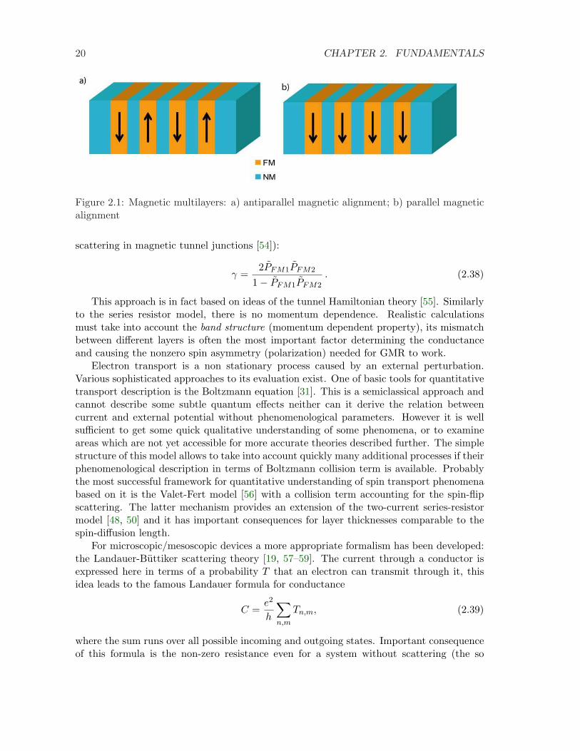
Simple magnetic multilayer can be built according to Fig. 2.1, it consists of alternatingferromagnetic (FM) and nonmagnetic (NM) layers. Current can flow through the structureeither in the in-plane direction (CIP) or perpendicular to planes (CPP). The latter case leadsto higher MR values and will be described here. The origin of GMR effect in multilayerscan be roughly explained by the two-current and series resistor model [48, 50]: In oneof possible multilayer realizations the interlayer exchange coupling [1] forces the magneticlayers to align antiparallel (AP) under zero magnetic field (Fig. 2.1 (a)). An appliedmagnetic field reverts all magnetizations to one direction (parallel magnetizations - PMstate, Fig. 2.1 (b)). Let us assume that all FM and NM layers are the same and denote theresistances of NM | FM↑| NM and NM | FM↓| NM part of system for spin-↑ electrons asRmaj , Rmin, respectively. Spin-↓ electrons experience the oppositely assigned resistances,i.e. Rmaj for FM↓ and vice versa. If Rmaj 6= Rmin, in the PM arrangement electrons inthe majority spin channels always experience only the more conducting channel, while inthe AP arrangement all electrons meet layers with alternating Rmaj and Rmin regardlessof its spin. We introduce the average resistance R and spin asymmetry β(β = P/ (P + 1)),so that Rmaj = 2R (1− β) and Rmin = 2R (1 + β). The resistance of the PM arrangementis RPM = R
(1− β2
)per two consecutive FM layers, while for the AP arrangement it is
RAP = R. The first one is obviously bigger for β 6= 0; we will typically work here with thecorresponding conductances CPM = R−1
PM , CAP = R−1AP . AP / PM switching can be also
accomplished by employing consecutive FM layers with different switching fields or usingsome other way to pin a subset of FM layers to a different magnetization direction thanother ones. The simplest structures where magnetoresistance can be achieved compriseonly two FM layers (NM | FM1 | NM | FM2 | NM junction), which we will refer to as spinvalves here. The magnetoresistance ratio is defined in this work as
γ =CPM
CAP− 1 . (2.37)
The nonmagnetic spacer between FM layers can be replaced by a semiconductor or aninsulator. Such structure comprising only two magnetic layers (FM1 and FM2) is referredto as the magnetic tunnel junction (MTJ). The corresponding analogue of GMR is thetunneling magnetoresistance (TMR) [3, 51], first successful realizations with non-negligibleTMR ratio at room temperature were realized in 1995 [52, 53], inspired by the success of theGMR. Its size is determined mainly by the spin polarization of density of states at the Fermienergy: P = (N↑ −N↓) / (N↑ +N↓). This allows to formulate a very simplified relationfor it, Julliere’s formula (named after the author of first observation of spin-dependent
20 CHAPTER 2. FUNDAMENTALS
Figure 2.1: Magnetic multilayers: a) antiparallel magnetic alignment; b) parallel magneticalignment
scattering in magnetic tunnel junctions [54]):
γ =2PFM1PFM2
1− PFM1PFM2
. (2.38)
This approach is in fact based on ideas of the tunnel Hamiltonian theory [55]. Similarlyto the series resistor model, there is no momentum dependence. Realistic calculationsmust take into account the band structure (momentum dependent property), its mismatchbetween different layers is often the most important factor determining the conductanceand causing the nonzero spin asymmetry (polarization) needed for GMR to work.
Electron transport is a non stationary process caused by an external perturbation.Various sophisticated approaches to its evaluation exist. One of basic tools for quantitativetransport description is the Boltzmann equation [31]. This is a semiclassical approach andcannot describe some subtle quantum effects neither can it derive the relation betweencurrent and external potential without phenomenological parameters. However it is wellsufficient to get some quick qualitative understanding of some phenomena, or to examineareas which are not yet accessible for more accurate theories described further. The simplestructure of this model allows to take into account quickly many additional processes if theirphenomenological description in terms of Boltzmann collision term is available. Probablythe most successful framework for quantitative understanding of spin transport phenomenabased on it is the Valet-Fert model [56] with a collision term accounting for the spin-flipscattering. The latter mechanism provides an extension of the two-current series-resistormodel [48, 50] and it has important consequences for layer thicknesses comparable to thespin-diffusion length.
For microscopic/mesoscopic devices a more appropriate formalism has been developed:the Landauer-Buttiker scattering theory [19, 57–59]. The current through a conductor isexpressed here in terms of a probability T that an electron can transmit through it, thisidea leads to the famous Landauer formula for conductance
C =e2
h
∑n,m
Tn,m, (2.39)
where the sum runs over all possible incoming and outgoing states. Important consequenceof this formula is the non-zero resistance even for a system without scattering (the so
2.4. CONDUCTANCE FROM THE LINEAR RESPONSE THEORY 21
called ballistic conductor), where the conductance is limited by the finite number of incom-ing/outgoing channels. This phenomenon, the Sharvin or contact resistance, may play roleonly in nanoconstrictions. If one would want to obtain the resistance of multiple interfacesfrom the knowledge of each interface resistance within the spirit of the series resistor model,he must take into account the fact that Sharvin resistance is then added to each interfaceas an artifact of the Landauer formulation. An advantage of the Landauer approach is thefact that it allows for an extension to finite bias situations, where it in fact resembles thenon-equilibrium Green’s function formalism [19]. Within linear response regime the Lan-dauer formalism has been shown to be equivalent [60] to the Kubo theory [17] employed inour calculations and presented in the next section.
2.4 Conductance from the linear response theory
The conductance calculation is restricted here to the static (zero-frequency) case and thelinear response regime, where the external perturbation causes only an infinitesimal shiftof system from its ground state. The perturbation operator B acts as an additional termin the Hamiltonian: H → H + eαtB, where α→ 0+ ensures good analytical properties fora derivation in terms of Green’s functions. The observable in question is associated witha hermitean operator A, its Heisenberg representation is A (t) = eiHtAe−iHt. Their linearresponse coefficient can be obtained from the general Kubo formula [18, 35] and is given by
CAB = −i limα→0+
∫ ∞
−∞dte−αtϑ (t)Tr
f (H)
[A (t) , B
]. (2.40)
We define an operator
A = ˙B = −i[B,H
], (2.41)
and an operator B for whichA = B = −i [B,H] . (2.42)
An important achievement of the linear response theory, the Kubo formula for con-ductance [17], is employed to express CAB conveniently. In order to derive the chargeconductance, one typically starts with its canonic form:
C(C)
AB= π
∫dξf ′ (ξ)Tr
Aδ (ξ −H) Aδ (ξ −H)
. (2.43)
In this work we will deal also with other kinds of linear response than the charge conduc-tance. A more general form of the Kubo formula must then be used because some commonassumptions must not be valid, although the result may also be called conductance. There-fore we sketch here a derivation starting from general formula (2.40). Operator A (t) isreplaced by its Schrodinger representation, two energy integrations are employed for theintegrand C ′
ABof (2.40):
C ′AB
= e−αtϑ (t)∫ ∞
−∞dξ
∫ ∞
−∞dηei(ξ−η)tTr
f (H)
[δ (ξ −H)Aδ (η −H) , B
], (2.44)
22 CHAPTER 2. FUNDAMENTALS
where the δ- function properties allows to replace H by energy arguments:
C ′AB
= e−αtϑ (t)∫ ∞
−∞dξ
∫ ∞
−∞dηei(ξ−η)t [f (ξ)− f (η)] Tr
δ (ξ −H)Aδ (η −H) B
.
(2.45)Going back to complete CAB and integrating over time leads to the following equation:
CAB = limα→0+
∫ ∞
−∞dξ
∫ ∞
−∞dηf (ξ)− f (η)ξ − η + iα
Trδ (ξ −H)Aδ (η −H) B
. (2.46)
Using the definition of Green’s functions (2.4) yields this formula:
CAB = limα→0+
∫dξf (ξ)Tr
δ (ξ −H)AG (ξ + iα) B +G (ξ − iα)Aδ (ξ −H) B
. (2.47)
The evaluation of the limit α→ 0+ is complicated by the fact that the operator B can benon-zero in an infinitely large area in contrast to the operator A. Therefore it is desirable torecast Eq. (2.47) into form explicitly restricted by operators A or A, which can be assumedto be localized in a finite region.
The general derivation of CAB shown in Appendix A leads to the following formula:
CAB = C(1)
AB+ C
(R)
AB, (2.48)
where
C(1)
AB= − i
2
∫dξf ′ (ξ)Tr
Aδ (ξ −H) AG (ξ − i0)−AG (ξ + i0) Aδ (ξ −H)
, (2.49)
and the remaining part is
C(R)
AB=
14π
∫dξf (ξ)Tr
AG (ξ + i0) AG2 (ξ + i0)−AG2 (ξ + i0) AG (ξ + i0)
−AG (ξ − i0) AG2 (ξ − i0)−AG2 (ξ − i0) AG (ξ − i0). (2.50)
A more transparent transcription of C(R)
ABis available, it is decomposed into two terms and
the total response coefficient is then given as
CAB = C(1)
AB+ C
(2)
AB+ C
(3)
AB, (2.51)
where
C(2)
AB= −1
2
∫dξf ′ (ξ)Tr
δ (ξ −H)
(BA− BA
), (2.52)
C(3)
AB= − i
2
∫dξf (ξ)Tr
δ (ξ −H)
(BB −BB
). (2.53)
The term C(1)
ABis equivalent to C(C)
ABin some situations. One can see that additional terms
to formula (2.43) appeared, C(2)
ABis for example present when Hall resistances are derived
2.4. CONDUCTANCE FROM THE LINEAR RESPONSE THEORY 23
[61]. Note that C(3)
ABcontains the Fermi-Dirac distribution instead of its derivative, hence
even for zero temperature the energy integration would not reduce just to the Fermi energy.There is a general rule which guarantees that the terms CAB reduces only to C(1)
AB, which
becomes equivalent to Eq. (2.43). It is valid even for case when an operator B cannot befound for A and the decomposition (2.51) is not possible. In order to satisfy this rule, theremust exist a regular operator U and a scalar ε ∈ −1, 1 so that the operators A, B, Hhave the following properties with respect to its transposition:
HT = UHU−1 ,
BT = εUBU−1 ,
AT = −εUAU−1 . (2.54)
To prove this, we first note that assumptions (2.54) lead quickly to GT (z) = UG (z)U−1
and another similar relation:
AT = −i(BH −HB
)T= −iεU
(HB − BH
)U−1 = −εUAU−1 . (2.55)
Note that the first and third term in Eq. (2.50) differ only by the choice of energy substitu-tion z = ξ+ i0 or z = ξ− i0. We label the common expression for these terms as C(R,1)
AB(z),
and analogously C(R,2)
AB(z) for the second and fourth term. Employing the general identity
TrM = TrMT for the first one we find
C(R,1)
AB(z) = TrAG (z) AG2 (z) = Tr[G2 (z)
]TATGT (z)AT . (2.56)
Substitution of the already known transposes of involved matrices shows that the term(2.56) turns into the second (or fourth) term C
(R,2)
AB(z) of Eq. (2.50):
C(R,1)
AB(z) = TrAG2 (z) AG (z) = C
(R,2)
AB(z) .
These two terms with opposite sign cancel and C(R)
ABvanishes.
One example of linear response satisfying conditions (2.54) is described in the followingsection, other can be found in Sec. 4.3 and 5.2.1.
2.4.1 Charge conductance
The starting point is the choice of the position operator X (r) as the response operator:B = X (r). If the operator X (r) is defined as a Cartesian coordinate at a point r, the oper-ator A then equals the velocity operator, which is useful to examine charge conductivity. Ifthe operator X (r) is defined as a projector to a given subspace, the operator A = −i [X,H]gives the flux from/into the subspace, which corresponds to calculation of charge conduc-tance through the surface of the subspace. B = ϕ (r) is a profile of a spin-independentexternal electrostatic field. One can quickly show that this kind of linear response fulfillsthe conditions (2.54), this is achieved with the choice U = 1 and ε = 1.
24 CHAPTER 2. FUNDAMENTALS
Substituting these operators into Eq. (2.43) leads to the Kubo formula for conductance(or conductivity) :
C = −2π∫
dξf ′ (ξ) Tr [X,H] δ (ξ −H) [ϕ,H] δ (ξ −H) , (2.57)
where the additional pre-factor 2 comes from atomic units expression of electron charge e2
present in conductance formula. Only zero temperature conductance is considered here,hence f ′(E) = −δ(E − EF ) and the energy integration reduces to an evaluation at theFermi energy. Substitution of Eq. (2.5) to (2.57) leads to:
C (EF ) = − 2π
Tr ImGr (EF ) [X,H] ImGr (EF ) [ϕ,H] . (2.58)
In the LMTO method the commutator [X,H] reduces to [X,S] simply because the remain-ing terms from H are diagonal in position as well as X. The same is valid for [ϕ,H]. Itsversion expressed in an arbitrary LMTO representation α is given as
C (EF ) = − 2π
Tr Im gα (EF + i0) [X,Hα] Im gα (EF + i0) [ϕ,Hα] , (2.59)
and it is invariant with respect to the representation (denoted by α) [62]. It has beenproved that this formula is correct up to second order in energy ε = E − Eν [62]. Thederivation was actually done for a form with a commutator [X,Sα] instead of[ϕ,Hα], butthe same argumentation can be applied. The index related to LMTO representation (α)will be omitted in the subsequent text.
The quantity of interest is the CPP charge conductance in layered systems. Note thatthe system is always attached to leads which allow electrons to enter or leave the structure.They are described by surface Green’s function as was explained in Sec. 2.2.3. The tracein Eq. (2.59) is restricted to the intermediate region, where Green’s functions fulfill Eq.(2.35). It allows us to write
(gr − ga) = gr (Σr − Σa) ga = ga (Σr − Σa) gr , (2.60)
where we introduced the retarded and advanced form of self-energy (embedding potentialof leads, Eq. 2.36) in the same way as for the corresponding Green’ functions. The anti-hermitean part of embedding potentials (self-energies) ΣL,R will be denoted here as BL,Rinstead of the commonly used Γ in order not to confuse it with vertex corrections Γ in thenext part:
B = i (Σr − Σa) , (2.61)BL,R = i
(ΣrL,R − Σa
L,R). (2.62)
Eq. (2.59) can be then rewritten as:
C (EF ) = − 12π
Tr Bgr[X,H]grBga[ϕ,H]ga . (2.63)
Employing [X,Σr] = 0 we find that
gr[X,H]gr = gr[X,E −H − Σr]gr = grX −Xgr , (2.64)
2.4. CONDUCTANCE FROM THE LINEAR RESPONSE THEORY 25
with a similar relation valid for [ϕ,Σa] this leads to
C (EF ) = − 12π
TrB(grX −Xgr)B(gaϕ− ϕga) . (2.65)
From this equation it is clear that only the (constant) values of the functions X(r)and ϕ(r) inside the leads enter the resulting conductance, it is therefore independent ofthe actual spatial profile of the potential. Note that this statement need not hold for acconductance, as was shown for a quantum wire in [63]. In order to obtain conductancethrough the intermediate region we consider Eq. (2.61) and take the profiles such that theunitary field is generated inside the left lead (X = 0 and ϕ = −1 there) while the responseto it (current) is measured inside the right lead (X = 1 and ϕ = 0 there) :
BX = XB = BR , Bϕ = ϕB = −BL , XBϕ = ϕBX = 0 . (2.66)
Charge unit e was already employed in (2.57), which justifies the choice of unitary potentialand current as 1. The negative value of the chosen ansatz for ϕ ensures that commutators[X,H] , [ϕ,H] picks elements of H going in one direction with the same sign (Sp,p′ for p′ > pand −Sp,p′ for p′ < p) consistently with the physical meaning of current. Relations (2.66)yield a compact Caroli-like [64] expression for conductance:
C (EF ) = − 12π
Tr BRgrBLga + BLgrBRga . (2.67)
It is a sum of two terms of the form
C (EF ) = −C (EF + i0, EF − i0)− C (EF − i0, EF + i0) ,
C (zµ, zν) =12πTr g (zµ)BLg (zν)BR . (2.68)
If the system is invariant with respect to the reversal of time, the terms C (EF + i0, EF − i0)and C (EF − i0, EF + i0) are equal. In transport calculations presented here the values±10−7 Ry were taken as the imaginary parts of energy arguments zµ and zν .
An alternative derivation of this formula can be seen in the appendix of Ref. [65]. Thedefinition of surface Green’s functions (SGF) [34] together with the partitioning technique[66]allows one to derive relations (A16 of Ref. [65]), with which the products of current oper-ators and system Green’s functions are replaced by embedding potentials ΣL,R (Eq. 2.36).
The formula (2.68) is obviously analogous to the transmission probability in the Lan-dauer formulation of transport [19]. The relation between the Kubo formulation and trans-mission matrices has been examined in [67]. If, for example, Eq. (2.68) is applied to apure infinite wire (ballistic conductor), its contact resistance is obtained as in the Landauerpoint of view [19].
For spin-dependent systems within the two-current model (Sec. 2.3) the two spin chan-nels are independent. Spin-resolved conductances C↑, C↑ can be derived directly fromformula (2.68), where Green’s functions for the corresponding spin state are employed:
Cs (zµ, zν) =12π
tr (gs (zµ)BLgs (zν)BR) , s = ↑, ↓ . (2.69)
All relations valid for Eq. (2.68) are valid also for (2.69) as long as no spin-dependentoperations are involved.
26 CHAPTER 2. FUNDAMENTALS
2.5 Substitutional disorder
Interfaces between two different materials are hardly completely clean and distinct. Becauseof manufacturing limitations and additional thermal processes, atoms of one species (A)can diffuse to the other one (B) and vice versa. This interface interdiffusion creates sub-stitutional disorder at few monolayers near the interface. It means that its lattice sites areoccupied by one of atoms Q, where Q ∈ A,B, but lattice geometry remains unchanged.Generally the number of species Q is unlimited. The occupation of the site R by the atomQ is described by ηQ
R ∈ 0, 1, and∑
Q ηQR = 1.
Alloys represent substitutional disorder not limited to only a few monolayers. Bulkdisorder can be intrinsic property of the material, it can also be a defect present undersome conditions. In any case its presence has often a strong impact on transport and otherproperties and may lead to some unique phenomena [68].
2.5.1 Configurational averages
One particular realization of occupations of the lattice sites is called a configuration C.Physical observables are obtained as averages of the observable’s mean value 〈X〉 over allpossible configurations weighted with their probabilities p (C):
〈〈X〉〉 =∑
C
p (C) 〈X〉 (C) . (2.70)
Common assumption here is complete randomness of occupations, given by probabilities(concentrations) cQR, with no short range order or correlations. The probability of oneconfiguration is then given as:
p (C) =∏
R
∑
Q
cQRηQR
. (2.71)
Very useful tool for dealing with substitutional disorder are again Green’s functions.Their configurational averages 〈G〉 are related to the averaged particle density and thusthey allow us to extract relevant observables due to the Hohenberg-Kohn’s first theorem(Sec. 2.1). Their advantage is the possibility to treat the random configuration-dependentpart of Hamiltonian as a perturbation U : H (C) = H0 + U (C), where H0 is configuration-independent. Note that the configurationally averaged Green’ function 〈G〉 obtained bysubstitution into Eq. (2.70) has again the full translational symmetry of the original lattice.
For disordered systems the property called Bloch spectral function becomes particularlyuseful. In the case of a system with a 3D or 2D translational symmetry, one can transformthe density of states (Eq. 2.27) to reciprocal space and obtain the Bloch spectral function,which allows to examine how different parts of the BZ contribute to the total density ofstates. In bulk crystals without substitutional disorder discrete bands are formed and theBloch spectral function is reduced to δ-functions located at crystal eigenenergies, whichcorrespond to its band structure. For disordered systems the peaks in the Bloch spectralfunction are no longer δ-functions, their extent and relation to the peaks of the originalpure materials may be important to understand properties of the disordered system. Energybands of such system are thus not discrete.
2.5. SUBSTITUTIONAL DISORDER 27
The main problem is to find desired configurational averages without evaluating allpossible configurations. There are simple methods available: virtual crystal approximation(VCA), where the random perturbing potential U is replaced by its average; and self-consistent Born approximation (SCBA), which corresponds to first order of perturbationtheory [18]. However, these cannot describe real physical properties of disordered systemsquantitatively and cannot even catch some qualitative properties, for example the creationof split bands for strong disorder (big |UA − UB| as compared to the bandwidth).
2.5.2 Supercell method
One possible approach to this problem is stochastic: to evaluate a number of possible ran-dom configurations chosen with respect to prescribed concentrations and find its average.Infinite systems must be split into small clusters (supercells) with size allowing it to besolved in real space [69]. A random configuration is generated for one supercell, which isthen assumed to be repeated infinitely across the lattice (or a layer in case of 2D trans-lational invariance). This defines boundary conditions of the supercell as periodic. Thesplitting into finite supercells represents key question of the method, the sufficient size ofthe supercell is not known as well as the necessary number of trial configurations, oneshould always check whether the result converges when increasing supercell size and whatis the error due to its variation.
An advantage of this method is its relatively simple implementation. Everything isperformed here for one configuration so that no theory describing the effect of disorder mustbe employed. Therefore it can be used quite simply not only for one particle properties butalso two-particle ones, which is one of the common areas of its application [15, 70]. It canalso handle situations beyond the complete randomness assumption, i.e. short range order.
Unfortunately the supercell method has high computational demands. Concentrationsof involved species are employed only by the ratio of atoms of their species with respect tototal number of atoms in the supercell. In order to catch slight changes of concentrationsvery big supercell must be used, the demands may then grow to the maximum currentlyavailable computers can offer. On the other hand, the bigger the supercell, the less k vectorsmust be used in calculation to maintain equal accuracy [70].
2.5.3 Coherent potential approximation
The coherent potential approximation (CPA) [71] is a single-site approximation - each site ofthe lattice is examined as a single impurity in an effective medium. The total Hamiltonianof the system can be rewritten as
H = [H0 + Σ (z)] + [U − Σ (z)] , (2.72)
whereH0 is the part of the Hamiltonian independent of configuration and U is its configuration-dependent complement. The CPA self-energy Σ (z) (so far undefined) added to H0 corre-sponds in CPA to the effective medium and it is associated to Green’s function G, overbarsdenote CPA averaged quantities. The remaining part of Hamiltonian U − Σ(z) is nowtreated as a perturbation and the Dyson equation for the problem can be written:
G = G+ GT G . (2.73)
28 CHAPTER 2. FUNDAMENTALS
It is immediately visible that if G = 〈G〉, the Eq. (2.73) leads to the exact condition
〈T 〉 = 0 . (2.74)
The CPA has been shown to be the best single-site approximation [72]. The T -matrixcan be expanded as sums of site contributions T =
∑R TR, these contributions are ex-
pressed in terms of single impurity scattering matrix tR [31]: TR = tR + tRG∑′
R′ TR′ ,where the prime at the sum denotes exclusion of R′ = R. Statistical correlations betweentR and TR′ are neglected, which is partially justified by the complete randomness of occu-pations, this is the so called CPA decoupling. Then a simple condition can be derived fromEq. (2.74) also for tR :
〈tR〉 =∑
Q
cQtQR (z) = 0 . (2.75)
The scattering matrix is required to behave so that scattering at a single site from themedium vanishes on average. This is the Soven equation [71] for CPA, which allows to findthe CPA self-energy. The self-energy is also decomposed into site contributions: Σ (z) =ΣR (z). Matrices tR can be expressed in terms of these contributions:
tR = [UR − ΣR (z)]1− G (z) [UR − ΣR (z)]
−1. (2.76)
Substituting (2.76) into (2.75) allows to find the unknown CPA self-energy Σ (z). Theexact condition (2.74) is then fulfilled with high accuracy, the only error is due to theCPA decoupling. This is the desired state, the CPA-averaged Green’s function G resemblesclosely the true configurational average of the system.
CPA can be conveniently combined with the TB-LMTO method [73]. This leads toan elegant formulation of the CPA-averaged auxiliary Green’s function in the form of Eq.(2.24):
g(z) = [ P(z) − S ]−1 , (2.77)
where P (z) is defined by this equation and is called a coherent potential function, LMTOrepresentation indices are omitted. Due to the single-site character of the CPA it is site-diagonal: PR,R′ (z) = δR,R′PR (z). For an atom Q in the effective medium described bythe coherent potential one can rewrite the formula (2.76) in terms of the coherent potential:
tQR(z) =(PQ
R (z)− PR(z)) [
1 + gR,R(z)(PQ
R (z)−PR(z))]−1
. (2.78)
For a binary alloy combining this equation with the CPA equation for t-matrices (2.75)leads to the following formula for the coherent potential function:
PR(z) = 〈 PR(z) 〉+ (PA
R(z)− PR(z))gR,R(z)
(PB
R (z)− PR(z)). (2.79)
A general solution for alloys with arbitrary number of components can be found in Chap.10.7 of [34]. The coherent potential function is obtained in an iterative process which shouldlead to self-consistency. There are numerous particular schemes of this iterative process [34]and it is often combined with the DFT iteration scheme.
Chapter 3
CPP conductance in disorderedmetallic multilayers
The CPA is widely used to determine electronic structure of disordered systems. For two-particle observables, for example the conductance, there are additional obstacles to besolved, which are addressed in Sec. 3.1. The Kubo formula for conductance has beencombined with the CPA a long time ago [74]. Its ab initio KKR implementation for residualresistivity of random bulk alloys [75] has been used by many authors [76–78]. However,for layered systems it has been applied only exceptionally, being confined mostly to modelswith a single orbital per site [79] or to a weak scattering limit [80]. In work [14] we haveapplied for the first time the coherent potential approximation to this problem on an abinitio level, which is the approach presented here. Its results are compared to supercellmethod results where possible, see sections 6.2.2, 6.3, 6.4.1.
3.1 CPA averages of two-particle observables, vertex correc-tions
In general, the Kubo formula (2.57) can be expressed so that it contains terms of the formTr G (zµ)BG (zν)B′. Current operators B, B′ are nonrandom within the TB-LMTOmethod, thus configurational averages of the following form are to be found:
K (zµ, zν) = 〈G (zµ)BG (zν)〉 . (3.1)
Configurational average of a product of two Green’s functions corresponds to a two-particleGreen’s function and it generally includes more complicated multiple-scattering processesthan those included in the one particle Green function described in sec. 2.5. Since theoperator B is nonrandom, after substituting the Dyson equation (2.73) into (3.1) andemploying (2.74) one obtains :
〈GBG〉 = GBG+ GΓG , (3.2)
where Γ =⟨TGBGT
⟩and energy arguments are omitted for brevity. The simple contribu-
tion corresponding to one-particle diagrams given as GBG will further be denoted as the
29
30 CHAPTER 3. CPP CONDUCTANCE IN DISORDERED MULTILAYERS
coherent part. Vertex corrections to it given by term GΓG represent genuine two-particlecorrelation effects [18]. This contribution to 〈GBG〉 in many cases cannot be neglected, aswill be shown further.
Vertex corrections can be derived with the same assumptions as the CPA self-energy,namely the CPA decoupling. No diagrammatic expansion is involved here. Due to thelocalized nature of the single-site T-matrices tR (z), Γ can be decomposed within the CPAinto a sum of site-localized contributions:
Γ =∑
R
ΓR . (3.3)
A closed set of exactly soluble linear equations for unknown ΓR has been derived [74]:
ΓR (zµ, zν) =⟨tR (zµ) G (zµ)BG (zν) tR (zν)
⟩+∑
R′(6=R)
⟨tR (zµ) G(zµ)ΓR′ (zµ, zν) G (zν) tR (zν)
⟩. (3.4)
Vertex corrections satisfy an important consistency condition, the Ward identity:
Γ (zµ, zν , 1) =−1
zµ − zν (Σ (zµ)− Σ (zν)) , (3.5)
where the third argument of Γ specifies the operator to which it corresponds. Satisfactionof this identity is natural since the derivation of vertex corrections is compatible with theself-energy.
3.2 LMTO full CPA solution for conductance
Vertex corrections have been shown to vanish for conductivities in a single band model [74].However, this is not true for a multiband case. We express the abstract set of Eqs. (3.4)in the TB-LMTO basis (Sec. 2.2) and solve it.
The equation for ΓR in terms of the matrix elements (energies omitted) :
ΓL1L′1R =
∑
Q
∑
L2L′2
cQRtQ L1L2
R [gBg]L2L′2RR t
Q L′2L′1R +
∑
Q
∑
R′(6=R)
∑
L2L′2L3L′3
cQRtQ L1L2
R gL2L3RR′ ΓL3L′3
R′ gL′3L′2R′R t
Q L′2L′1R . (3.6)
They can be formally simplified by introducing the following composed indices and auxiliaryvariables:
Λ =(L,L′
), (3.7)
ξΛ1R (zµ, zν) = ξ
L1L′1R (zµ, zν) = (g (zµ)Bg (zν))
L1L′1RR , (3.8)
ωΛ1Λ2R (zµ, zν) =
∑
Q
cQRtQ L1L2
R (zµ) tQ L′2L′1R (zν) , (3.9)
3.3. CPP CONDUCTANCE IN DISORDERED MULTILAYERS 31
χΛ1Λ2RR′ (zµ, zν) = (1− δRR′) g
L1L2RR′ (zν) g
L′2L′1R′R (zν) . (3.10)
The original Eqs. (3.6) are then rewritten compactly as:
ΓΛ1R =
∑
Λ2
ωΛ1Λ2R ξΛ2
R +∑
R′;Λ2Λ3
ωΛ1Λ2R χΛ2Λ3
RR′ ΓΛ3R′ , (3.11)
where energy arguments have been omitted for brevity. Matrices with one R index aretreated here as if were multiplied by δRR′ . The set of equations (3.11) for Γ is solved bymatrix inversion, which yields the following matrix equation:
Γ = (1− ωχ)−1 ωξ =(ω−1 − χ)−1
ξ . (3.12)
Auxiliary variables can be defined in a slightly different way, which leads to a solution moresuitable for a direct calculation:
λ−1 = ω−1 + ϕ , (3.13)
whereϕΛ1Λ2
R (zµ, zν) = gL1L2RR (zµ) gL′2L′1
RR (zν) . (3.14)
Then the matrix equation for vertex corrections reads:
Γ =(λ−1 − ψ)−1
ξ , (3.15)
where ψΛ1Λ2R1R2
(zµ, zν) = gL1L2R1R2
(zµ) gL′2L′1R2R1
(zν), hence it fulfills χ = ψ−ϕ. The advantage isthat λ is site-diagonal and ψ has a more simple structure than χ, which allow to performlattice Fourier transformation easily. The central matrix is given its name:
∆ = λ−1 − ψ . (3.16)
The equation for vertex corrections with explicit typing of all indices reads:
ΓΛ1R1
(zµ, zν) =(∆−1
)Λ1Λ2
R1R2(zµ, zν) ξΛ2
R2(zµ, zν) . (3.17)
3.3 CPP conductance in disordered multilayers
With the knowledge of vertex corrections the conductance can be derived directly fromthe formula (2.68). As both operators BL and BR are nonrandom, one of them can beput out of the configurational average; the remaining part to be averaged corresponds tothe product of two Green’s functions and an operator, which already appeared in equation(3.1), the second one from operators BL,R is identified with the generic operator B. Hence(3.2) can be employed and the main term in conductance expression is also expanded intothe coherent and VC part:
Tr 〈g (zµ)BLg (zν)BR〉 =Tr g (zµ)BLg (zν)BR+ Tr g (zµ) Γg (zν)BR . (3.18)
32 CHAPTER 3. CPP CONDUCTANCE IN DISORDERED MULTILAYERS
The coherent part is similar to the case without disorder, but now the auxiliary Green’sfunction g (z) is replaced by its configurationally averaged counterpart g. The trace propertyfor the VC part is employed:
CV C (zµ, zν) =12π
Tr g (zµ) Γg (zν)BR =12π
Tr g (zν)BRg (zµ) Γ . (3.19)
Substituting Γ from (3.17) leads to:
CV C (zµ, zν) =12π
∑
R1Λ1
∑
R2Λ2
[g (zν)BRg (zµ)]Λ1
R1
[∆−1 (zµ, zν)
]Λ1Λ2
R1R2[g (zµ)BLg (zν)]
Λ2
R2,
(3.20)where the index Λ means Λ with a transposed order of orbital indices and the quantityξ (zµ, zν) is now labeled as [g (zµ)BL,Rg (zν)] to make its close relation to operators BL, BRmore transparent. The result is again explicitly symmetric in BL, BR, although vertexcorrections were expressed with respect to only one of the operators during the derivation.
Multilayers can be viewed as systems with 2D translational invariance, there are alwaystwo dimensions much larger than electron mean free path and the corresponding boundariesdoes not play role, contrary to its thickness, which is on the nanoscale. In disorderedsystems, the 2D translational invariance is destroyed, but the effective system replacing thephysical one is again translationally invariant. This is greatly facilitated in calculations ofGreen’s functions, where the 2D lattice Fourier transformation from the real to reciprocalspace is then employed (Sec. 2.2.3). Matrix quantities in real space transform according toEq. (2.29), the opposite transformation is given by (2.30). Generally the site position vectorR is decomposed as R ≡ (p,B,T‖) as described in Sec. 2.2.3. The quantities involved inEq. (3.20) expressed in terms of k‖-resolved Green’s functions:
∆ (0, zµ, zν)Λ1Λ2
p1,B;p2,B2= δp1B1;p2B2
[λ−1 (zµ, zν)
]Λ1Λ2
p1B1−
1N
∑
k‖
gL1L2p1B1;p2B2
(k‖, zµ
)g
L′2L′1p2B2;p1B1
(k‖, zν
). (3.21)
[g (zµ)BRg (zν)]ΛpB =
1N
∑
k‖
∑
LaBa
∑
LbBb
gLLapB;pRBa
(k‖, zµ
)B LaLbRBa;Bb
(k‖
)gLbL
′pRBb;pB
(k‖, zν
)
(3.22)Note that they are independent of k‖ as well as T‖, which significantly simplifies the cal-
culation. The first expression is nothing but the lattice Fourier transform for zero k‖ vectorof the matrix ∆Λ1Λ2
R1R2(zµ, zν), Eq. (3.16). The formula for VC contribution to conductance
is then given as [14]:
Tr 〈g (zµ)BLg (zν)BR〉V C = (3.23)12π
∑
p1B1Λ1
∑
p2B2Λ2
[g (zν)BRg (zµ)] Λ1p1,B1
[∆−1 (0, zµ, zν)
]Λ1 Λ2
p1,B1;p2,B2[g (zµ)BLg (zν)] Λ2
p2,B2.
Equation (4.41) together with the definitions of auxiliary variables (Eqs. 3.21,3.22, 3.13)represents the central result of this chapter and was implemented in an ab initio calculation
3.3. CPP CONDUCTANCE IN DISORDERED MULTILAYERS 33
scheme. The matrix ∆ to be inverted is of the size l4maxN2, where N =
∑Np=1 Np and Np
denotes the number of disordered basis atoms in one principal layer p. This can yield forexample matrices of the order 1000 × 1000 for (Ga,Mn)As slab containing 12 principallayers, but the numerically demanding inversion of it has to be done for only one k‖ point.The smaller basis with respect to the supercell method (Sec. 2.5.2) leads to a significantperformance gain of the full CPA scheme, although all subblocks of g
(k‖, z
)must be
evaluated here in contrast to the CPP conductance formula for a clean system (2.68) usedalso in supercell transport calculations, where only the layer-wise subblocks in corners (1, Nand N, 1) are needed. As the evaluation of the whole g
(k‖, z
)is the most time-consuming
part, it is advantageous to utilize the tridiagonal character of the Hamiltonian in space,this procedure then becomes roughly of order N2.
This CPA based method has been used to examine selected impure Co/Cu based mul-tilayers (Chap. 6), thin layers of (Ga,Mn)As (Chap. 7) and possible disorder in Co2MnSi(Chap. 8). In the first case results were compared to alternative supercell calculations andtheir overall agreement confirms the validity of this approach. The presented derivationcan be also adapted to spin-mixing conductances, see Sec. 4.5.
3.3.1 Lattice point group symmetry
In addition to translation symmetry, lattice point group symmetry represents an importantfactor influencing the solid properties. If it is utilized in ES and transport calculations,it allows to evaluate general quantities X for k-points only inside the irreducible Brillouinzone (IBZ), while the rest of the total Brillouin zone (BZ) can be obtained from appropriatesimilarity transformations U (O) [34], where O are symmetry operations. This rests on theexistence of matricesM andM ′ such thatX for vectorsOk outside the IBZ can be expressedas
X (Ok) = M (O)X (k)M ′ (O) . (3.24)
This provides significant reduction of calculation time and memory requirements. Its imple-mentation in CPA transport for disordered systems is not so straightforward as for systemswithout disorder, but in principle it can reduce the amount of k-points to calculate by thesame ratio, 1/ |NO|, where |NO| is the order of the group of allowed symmetry operations.The argumentation is valid for any translational symmetry, hence only vectors from Bril-louin zone will now be generally denoted as k. Quantities averaged over the whole BZ(XBZ) are expressed in the following way in terms of an IBZ-averaged quantities XIBZ :
XBZ =1|NO|
∑
OXIBZ (O) . (3.25)
Let us first examine the behavior of TB-LMTO Green’s functions: elements diagonal in Btransform as
gB,B (Ok) = U+ (O) gB,B (k)U (O) , (3.26)
which is already in the form of Eq. (3.24). Explicit matrix structure of similarity trans-formations is UL1,L2 , summations over these orbital indices L are omitted for brevity. Fortransformation of elements non-diagonal in B an additional factor (unitary matrix in orbitalindices)
fB (O,k) = eik(O−1B−B) (3.27)
34 CHAPTER 3. CPP CONDUCTANCE IN DISORDERED MULTILAYERS
is present:gB,B′ (Ok) = fB (O,k)U+ (O) gB,B′ (k)U (O) f−1
B′ (O,k) . (3.28)
BZ summations in Eqs. (3.21, 3.22) allows to utilize these properties of Green’s func-tions. Value of Eq. (3.22) for a part of BZ obtained by a symmetry operation O is given(with omitted explicit dependence of U (O) and fB (O,k) on O) as:
[g (zµ)Bg (zν)]pB (O) =1N
∑
k(IBZ)
∑
Ba
∑
Bb
fB (k)U+gpB,pRBa (k, zµ)Uf−1Ba
(k) fBa (k)U+
×BBaBb(k)Uf−1
Bb(k) fBb
(k)U+gpRBb,pB (k, zν)Uf−1B (k) .
All adjacent UU+ terms cancel, all fB (k) terms cancel with their counterpart f−1B (k).
Then
[g (zµ)Bg (zν)] (O) = U+ (O) [g (zµ)Bg (zν)]IBZ U (O) , (3.29)
where [g (zµ)Bg (zν)]IBZ is given by Eq. (3.22), but with the k-summation restricted only
to the irreducible Brillouin zone. This result has the form of Eq. (3.24), it is valid for eachk point from IBZ as well as the whole IBZ average.
For ψ (zµ, zν), the only k-dependent component of ∆ (0, zµ, zν) (Eq. 3.21), we firstexamine the effect of the inclusion of fB (k) and for clarity omit U , which commutes withfB (k):
ψL1L′1;L2L′2p1B1;p2B2
(O, zµ, zν) =∑
k(IBZ)
f−1B1
(k) gL1;L2p1B1,p2B2
(k, zµ) f−1B2
(k) fB2 (k) gL′2;L′1
p2B2,p1B1(k, zν) f−1
B1(k) .
(3.30)All fB (k) terms cancel here. The true ψ (zµ, zν) for the part of BZ corresponding tosymmetry operation O is given as:
ψL1L1
′;L2L′2
p1B1,p2B2(O, zµ, zν) =
=∑
L1L2L′1L′2
∑
k(IBZ)
(U+
)L1L1(U+
)L′1L′1 gL1L2p1B1,p2B2
(k, zµ) gL′1L′2p2B2,p1B1
(k, zν)UL2L2UL′2L′2
=∑
L1L2L′1L′2
(U+
)L1L1(U+
)L′1L′1 ψIBZ L1L′1;L2L′2p1B1,p2B2
(zµ, zν)UL2L2UL′2L′2 , (3.31)
where ψIBZ (zµ, zν) is given by Eq. (3.21), but with the k-summation restricted only to theirreducible Brillouin zone. The transformation k→ Ok is now performed by a proper mul-tiplication of submatrices of ψ by U matrices, it cannot be expressed in terms of compoundindices Λ, but it is still in the form of (3.24) suitable for the replacement of BZ averagingby IBZ one.
Chapter 4
Spin torques due to spinaccumulation
If a current incident on a thin ferromagnetic (FM) layer is polarized non-collinear withrespect to the layer magnetization direction, it exerts a spin-transfer torque on the magneticlayer and may change its magnetization direction [9]. This phenomenon is therefore referredto as the current induced magnetization switching (CIMS).
One of successful quantitative descriptions of this process is based on Valet-Fert model(Sec. 2.3), which has been recently extended to non-collinear spin structures [81–83]. Itrests heavily on two additional properties of spin currents (Sec. 5.1). First, the transverse(perpendicular to local exchange field) component of the spin current inside a ferromagnetbecomes rapidly damped on a typical distance of a few interatomic spacings [84]. This veryshort magnetic coherence length is a result of a large exchange splitting which leads tomostly destructive interference effects due to all contributions of wave vectors on the twoFermi surfaces of the ferromagnetic metal. Consequently, the spin torque experienced by aferromagnetic (FM) layer can be identified with the transverse spin current at its interfacewith a neighboring non-magnetic (NM) layer. Second, the proper boundary conditionsinevitable for a full solution of the diffusion equations must be formulated in terms ofproperties of individual interfaces and it comes out that more information is needed thancontained in the spin-resolved conductances of the interfaces.
The magneto-electronic circuit theory [15, 85, 86] represents another flexible approachto the transport properties of non-collinear magnetic systems consisting of FM and NMelements (nodes). This scheme is highly efficient especially when dimensions of individualnodes are smaller than the spin-diffusion lengths but bigger than the electron mean-freepaths of the corresponding materials. The theory is based on the semiclassical concept ofspin accumulation (Sec. 4.1). Within the developed formalism, the chemical potentialsand spin accumulations of the nodes are contained in 2 × 2 distribution matrices in thespin space. The change of spin current due to junctions among the nodes is related to thenon-collinear part of spin accumulation in terms of the so called spin-mixing conductance.The steady-state currents, spin currents and spin torques in a device can be obtained fromapplied voltages by solving a set of linear equations quite similar to the Kirchhoff’s lawsfor usual electronic circuits, see Ref. [15] for a review.
A truly microscopic (quantum mechanical) approach to all aspects of CIMS seems to
35
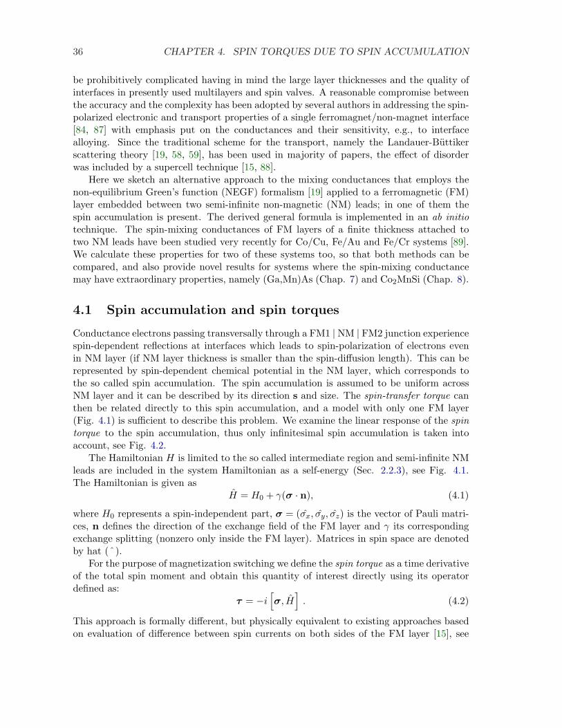
36 CHAPTER 4. SPIN TORQUES DUE TO SPIN ACCUMULATION
be prohibitively complicated having in mind the large layer thicknesses and the quality ofinterfaces in presently used multilayers and spin valves. A reasonable compromise betweenthe accuracy and the complexity has been adopted by several authors in addressing the spin-polarized electronic and transport properties of a single ferromagnet/non-magnet interface[84, 87] with emphasis put on the conductances and their sensitivity, e.g., to interfacealloying. Since the traditional scheme for the transport, namely the Landauer-Buttikerscattering theory [19, 58, 59], has been used in majority of papers, the effect of disorderwas included by a supercell technique [15, 88].
Here we sketch an alternative approach to the mixing conductances that employs thenon-equilibrium Green’s function (NEGF) formalism [19] applied to a ferromagnetic (FM)layer embedded between two semi-infinite non-magnetic (NM) leads; in one of them thespin accumulation is present. The derived general formula is implemented in an ab initiotechnique. The spin-mixing conductances of FM layers of a finite thickness attached totwo NM leads have been studied very recently for Co/Cu, Fe/Au and Fe/Cr systems [89].We calculate these properties for two of these systems too, so that both methods can becompared, and also provide novel results for systems where the spin-mixing conductancemay have extraordinary properties, namely (Ga,Mn)As (Chap. 7) and Co2MnSi (Chap. 8).
4.1 Spin accumulation and spin torques
Conductance electrons passing transversally through a FM1 | NM | FM2 junction experiencespin-dependent reflections at interfaces which leads to spin-polarization of electrons evenin NM layer (if NM layer thickness is smaller than the spin-diffusion length). This can berepresented by spin-dependent chemical potential in the NM layer, which corresponds tothe so called spin accumulation. The spin accumulation is assumed to be uniform acrossNM layer and it can be described by its direction s and size. The spin-transfer torque canthen be related directly to this spin accumulation, and a model with only one FM layer(Fig. 4.1) is sufficient to describe this problem. We examine the linear response of the spintorque to the spin accumulation, thus only infinitesimal spin accumulation is taken intoaccount, see Fig. 4.2.
The Hamiltonian H is limited to the so called intermediate region and semi-infinite NMleads are included in the system Hamiltonian as a self-energy (Sec. 2.2.3), see Fig. 4.1.The Hamiltonian is given as
H = H0 + γ(σ · n), (4.1)
where H0 represents a spin-independent part, σ = (σx, σy, σz) is the vector of Pauli matri-ces, n defines the direction of the exchange field of the FM layer and γ its correspondingexchange splitting (nonzero only inside the FM layer). Matrices in spin space are denotedby hat (ˆ).
For the purpose of magnetization switching we define the spin torque as a time derivativeof the total spin moment and obtain this quantity of interest directly using its operatordefined as:
τ = −i[σ, H
]. (4.2)
This approach is formally different, but physically equivalent to existing approaches basedon evaluation of difference between spin currents on both sides of the FM layer [15], see
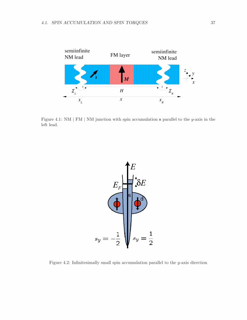
4.1. SPIN ACCUMULATION AND SPIN TORQUES 37
Figure 4.1: NM | FM | NM junction with spin accumulation s parallel to the y-axis in theleft lead.
Figure 4.2: Infinitesimally small spin accumulation parallel to the y-axis direction
38 CHAPTER 4. SPIN TORQUES DUE TO SPIN ACCUMULATION
Sec. 5.1.The well known algebraic rules for the Pauli matrices
(σ · p)(σ · q) = p · q + i(p× q) · σ,(σ · p)σ = p + iσ × p,
σ(σ · q) = q + iq× σ, (4.3)
valid for arbitrary classical vectors p and q, yield an explicit form of the torque operator
τ = 2γn× σ. (4.4)
This relation shows that the spin torque is a local operator non-zero only inside the inter-mediate region. Ab initio expression for the response CL of the spin torque to the spinaccumulation can be found using NEGF. An alternative approach based on the Kubo lin-ear response theory is also possible, we use it to derive a less general formula only for spintorque response in the direction parallel to the spin accumulation. NEGF based derivationfor this component of the total spin torque will be published elsewhere [90].
4.2 Derivation based on NEGF
The thermodynamic average of the spin torque τ for the NM|FM|NM system in a stationarynon-equilibrium state is given by
τ =12π
∫ ∞
−∞Tr
τG<(E)
dE, (4.5)
where G<(E) is the lesser component of the non-equilibrium Green’s function. The latterquantity is related to the retarded and advanced Green’s functions Gr(E) and Ga(E) bymeans of the kinetic equation
G<(E) = Gr(E)Σ<(E)Ga(E),Gr(E) = [E −H − Σr(E)]−1 ,
Ga(E) = [E −H − Σa(E)]−1 , (4.6)
where Σ<(E), Σr(E) and Σa(E) denote the lesser, retarded and advanced components ofthe self-energy, respectively, which are usually defined in NEGF formalism [19]. The totalself-energies are given as sums of separate contributions due to the left (L) and the right(R) leads,
Σx(E) = ΣxL(E) + Σx
R(E), x = r, a,< . (4.7)
These self-energies therefore correspond to embedding potentials (2.36) once the TB-LMTOformulation is assumed (Sec. 4.5). Note that all operators in Eqs. (4.5, 4.6) are defined inthe Hilbert space of the intermediate region.
The spin accumulation in the NM leads results in a change of the lesser self-energyδΣ<(E) (see below), which induces the following first-order change of the thermodynamicaverage (4.5):
δτ =12π
∫ ∞
−∞Tr
Ga(E)τGr(E)δΣ<(E)
dE. (4.8)
4.2. DERIVATION BASED ON NEGF 39
The special form of the torque operator, Eq. (4.2), together with the expression for Gr,a(E),Eq. (4.6), provide a relation
Ga(E)τGr(E) = −i [σGr(E)−Ga(E)σ] +Ga(E)σB(E)Gr(E), (4.9)
where the abbreviation for the antihermitean part of self-energy due to leads according toEq. (2.61, 2.62) is employed.
In deriving Eq. (4.9), use was made of the fact that the self-energies of the unperturbedNM leads are spin-independent, so that [σ,Σr,a(E)] = 0.
For stationary non-equilibrium systems without spin accumulation, the lesser self-energiesare given by
Σ<L,R(E) = fL,R(E)BL,R(E), (4.10)
where the functions fL,R(E) refer to the Fermi-Dirac distributions of the two leads.In the thermodynamic equilibrium, the distributions fL,R(E) coincide with the Fermi-
Dirac distribution of the whole system. In presence of the spin accumulation in one of theleads (L), the system is driven out of equilibrium by adding a spin-dependent shift δEL tothe Fermi energy of the lead. This yields the first-order change of the lesser self-energy ina form
δΣ<(E) = δΣ<L(E) = f ′(E)(σ · s)BL(E)δEL, (4.11)
where f ′(E) means the derivative of the Fermi-Dirac distribution and s is a unit vectorpointing in direction of the spin accumulation. For systems at zero temperature, which willbe considered in the following, f ′(E) = −δ(E−EF ) where EF is the Fermi energy. Substi-tution of Eqs. (4.9, 4.11) into Eq. (4.8) provides a starting expression for the correspondingresponse coefficient CL:
CL ≡ δτ
δEL=
12π
Tr [i(σGr −Gaσ)(σ · s)BL − σBGr(σ · s)BLGa] , (4.12)
where all omitted energy arguments equal the Fermi energy EF .In order to extract the dependence of the response coefficient CL on orientation of the
spin accumulation s and the magnetization direction n, the explicit structure of the Green’sfunctions Gr,a of the Hamiltonian (4.1) with respect to the spin must be used,
Gr,a =Gr,a↑ +Gr,a
↓2
+Gr,a↑ −Gr,a
↓2
(σ · n), (4.13)
where the spin-resolved Green’s functions are defined by
Gr,as (E) = [E −Hs − Σr,a(E)]−1 , s = ↑, ↓ . (4.14)
The substitution of Eq. (4.13) into Eq. (4.12) reduces its r.h.s. to a sum of terms of the formTr(ξX) = trS(ξ)tr(X) where ξ is a matrix in the spin indices only while X is a matrix inthe other (site and orbital) indices and where the symbols trS and tr denote the respectivetrace operations. Further steps employ the rules (4.3) and their consequences for tracerelations:
trS[σ(σ · s)] = 2s,trS[σ(σ · n)(σ · s)] = 2in× s,
trS[σ(σ · n)(σ · s)(σ · n)] = 4(n · s)n− 2s. (4.15)
40 CHAPTER 4. SPIN TORQUES DUE TO SPIN ACCUMULATION
The resulting expression for CL follows after a lengthy but straightforward manipulation:
CL = D1s +D2s× n−D3(n · s)n, (4.16)
where the prefactors D1, D2 and D3 are given by
D1 =12π
tr[i(Gr↑ +Gr
↓ −Ga↑ −Ga
↓)BL − BGr
↑BLGa↓ − BGr
↓BLGa↑],
D2 =12π
tr[(Gr↑ −Gr
↓ +Ga↑ −Ga
↓)BL + i
(BGr↑BLGa
↓ − BGr↓BLGa
↑)],
D3 =12π
tr[B (
Gr↑ −Gr
↓)BL
(Ga↑ −Ga
↓)]. (4.17)
The form of Eq. (4.16) can be simplified by using a general relation
i [Gr(E)−Ga(E)] = Ga(E)B(E)Gr(E) (4.18)
that follows from Eqs. (4.6, 2.62). After inserting the spin-resolved counterparts of Eq. (4.18),i(Gr
s −Gas) = Ga
sBGrs (s = ↑, ↓), in the expression (4.17) for D1 one obtains D3 = D1. The
previous formula (4.16) for the response coefficient CL can thus be rewritten as
CL = D1n× (s× n) +D2s× n. (4.19)
Note that this results has a general form of a vector perpendicular to n, in agreement withEq. (4.4). A closer inspection of the real quantities D1 and D2, Eq. (4.17), reveals theirsimple relation to a single complex quantity – the spin-mixing conductance Cmix
L :
CmixL =
12π
tr[i(Gr↑ −Ga
↓)BL − BGr
↑BLGa↓], (4.20)
which yieldsD1 = D3 = 2 ReCmix
L , D2 = 2 ImCmixL . (4.21)
The formulas (4.19, 4.20, 4.21) represent the central result of this Chapter. It is interestingto compare them to the well-known spin-resolved charge conductances, Eq. (2.69). We haveshown that these formulas are invariant with respect to the position of boundaries betweenthe leads and the intermediate region (Appendix B), which is an important feature for theconsistency of the theory and for practical calculations.
4.3 Derivation based on the Kubo theory
The real part of the spin mixing conductance Cmix can also be derived within the Kubolinear response approach and the result is equivalent to that from the NEGF derivation.The Hamiltonian is in the form of Eq. (4.1), but we set the magnetization direction alongthe z-axis for simplicity:
H = H0 + γσz, (4.22)
The setup of the system can be seen in Fig. 4.1. We employ the linear response theory(Sec. 2.4). The spin-transfer torque τα = −i[σα, H] is substituted as an operator in theform A = −i [B,H], and the perturbation operator is given as B = σyφ (x), where φ (x)
4.3. DERIVATION BASED ON THE KUBO THEORY 41
is the profile of the spin accumulation across layers and the spin accumulation is assumedto be parallel to the y-axis. Response coefficient CAB is in general given by three termsC(1), C(2) , C(3) (Eq. 2.51). If we consider only the most interesting situation, the spintorque in the direction of the spin accumulation, B = σy, the spin-transfer torque operatoris then
A = −i[σy, H
]= −i [σy,H0 + γσz] = 2γσx . (4.23)
The operator A is evaluated as follows:
A (x) = −i[B (x) , H
]= −i [φ (x) ,H0] σy + 2φ (x) γσx. (4.24)
Then the terms C(2) and C(3) vanish. Differently speaking this combination of A, B oper-ators satisfies the condition (2.54). The presence of C(3) would require an integration overthe whole energy range below Fermi level even at zero temperature, which would complicatethe solution. This term cannot be shown to vanish in the calculation of an out-of-planeresponse in the direction given by σx, therefore we examine only the first case here. Thenonly the term C(1) constitutes the linear response coefficient denoted Cmix
K , analogously tothe charge conductance solution and for zero temperature it is given by substituting into(2.43):
CmixK = π
∫dξf ′ (ξ)Tr 2γσxδ (ξ −H) (−i [φ,H0] σy + 2φγσx) δ (ξ −H) . (4.25)
Employing explicit spin structure of Green’s functions of collinear system (described in thepreceding section) and the zero temperature assumption we find after a few manipulations:
CmixK = − 2
πtr
2γImGr
↓ ([φ,H0] + 2φγ) ImGr↑
(4.26)
Both γ and [φ,H0] + 2φγ are localized to the intermediate region, hence the trace isevaluated only in that region. One can quickly find that for the Green’s functions definedas the resolvent of the Hamiltonian (4.22) the following relations hold:
Gr↑2γG
r↓ = Gr
↑ −Gr↓ , (4.27)
Ga↓2γG
a↑ = Ga
↑ −Ga↓ . (4.28)
Employing the relation between ImGrs and self-energies, Eq. (2.60) and the definition of
its anti-hermitean part (2.61), formula (4.26) can then be rewritten as
CmixK =
12π
trGr↑BφGa
↑B −Gr↑BGa
↓φB−−Gr
↓BφGa↑B +Gr
↓BGa↓φB
. (4.29)
Operators B are non-zero only at boundaries (interfaces to leads), therefore the responsedepends only on spin accumulation φ (x) at these boundaries, its arbitrary variations in theintermediate region are not significant. Consistently with Sec. 4.2 we express the responseto the spin accumulation in the left lead (L), hence limx→∞ φ (x) = φR = 0 and the profileis then normalized so that limx→−∞ φ (x) = φL = 1. This yields
CmixK,L =
12π
tr(Gr↑ −Gr
↓)BLGa
↑B −(Gr↑ −Gr
↓)BGa
↓BL. (4.30)
42 CHAPTER 4. SPIN TORQUES DUE TO SPIN ACCUMULATION
Note that during BZ averaging this quantity for each k‖ vector is summed togetherwith its time inversion corresponding to its appropriate −k‖vector and this inversion isrelated by symmetry operations to its origin: G
(−k‖)
= GT(k‖
). Using these operations
one can show that the NEGF result in the linear response limit for the real part of thespin-mixing conductance (quantity D3 in Eq. 4.17) is equivalent to that of the Kubobased approach (Eq. 4.30) if their sums together with their time-inversions are considered:∑
k‖ CmixK,L
(k‖
)=
∑k‖ 2ReCmix
L(k‖
). It has been also proved that an actual shape of
spin accumulation profile in the system is irrelevant for the real part of the spin-mixingconductance, it depends only on its values at interfaces to leads. In NEGF derivation weassumed spin accumulation to be present only in the leads and now this assumptions wasshown to be appropriate.
4.4 Comparison to scattering theory
The resulting dependence of the spin torque, Eq. (4.19) on the orientation of the spinaccumulation and the magnetization is identical to that obtained within the Landauer-Buttiker scattering theory of transport [15]. In order to make the relation of this traditionaltool to the present approach more explicit, we consider here the simplest case, namely aone-dimensional system with one propagating mode in both of the identical NM leads.
The configuration space of the system is a real axis with positions denoted by a continu-ous variable x (−∞ < x <∞), see Fig. 4.1. The spin-independent part of the Hamiltonianis given by H0 = −(∂/∂x)2 (atomic units are used) and the exchange splitting γ(x) vanishesfor x ≤ xL and x ≥ xR, where the points xL and xR denote the boundaries between the NMleads and the intermediate region containing the FM part. The Fermi energy correspondsto a positive kinetic energy in the leads, EF = k2 with k > 0.
The spin-resolved retarded and advanced Green’s functions Gr,as (s = ↑, ↓) at this real
energy are constructed from two independent solutions χ1s(x) and χ2s(x) of the Schrodingerequation for the Hamiltonians H↑ = H0 + γ and H↓ = H0− γ. The asymptotics of the twosolutions is
χ1s(x) = exp(ikx) for x ≥ xR,χ2s(x) = exp(−ikx) for x ≤ xL, (4.31)
and the retarded Green’s function is given by
〈x|Grs|x′〉 =
χ1s(x>)χ2s(x<)Ws
, (4.32)
where Ws = χ2s(x)[∂χ1s(x)/∂x] − χ1s(x)[∂χ2s(x)/∂x] denotes the (x-independent) Wron-skian of the two solutions while x> = maxx, x′ and x< = minx, x′.
The asymptotic behavior of the solution χ1s(x) for x ≤ xL is given by
χ1s(x) = t−1s [exp(ikx) + rs exp(−ikx)] , (4.33)
where we introduced the spin-resolved transmission (ts) and reflection (rs) coefficients ofthe wave incoming from the left. They satisfy the usual condition |rs|2 + |ts|2 = 1 and their
4.5. TB-LMTO-CPA FORMULATION AND IMPLEMENTATION 43
knowledge allows us to evaluate explicitly the Wronskian in Eq. (4.32), Ws = 2ikt−1s , as
well as the asymptotics of the solution χ2s(x) for x ≥ xR:
χ2s(x) =1ts
exp(−ikx)− r∗st∗s
exp(ikx). (4.34)
These relations yield, e.g., the following elements of the retarded Green’s functions:
〈xL|Grs|xL〉 =
12ik
[1 + rs exp(−2ikxL)] ,
〈xR|Grs|xR〉 =
12ik
[1− r∗sts
t∗sexp(2ikxR)
],
〈xL|Grs|xR〉 =
ts2ik
exp[ik(xR − xL)]. (4.35)
Other elements, including those of the advanced Green’s functions, can be obtained withhelp of general identities 〈x′|Gr
s|x〉 = 〈x|Grs|x′〉 and 〈x|Ga
s |x′〉 = 〈x|Grs|x′〉∗. Since the
antihermitean parts of the self-energy B = BL + BR, Eq. (2.62), are in this particular casegiven by
〈x|BL|x′〉 = 2kδ(x− xL)δ(x′ − xL),〈x|BR|x′〉 = 2kδ(x− xR)δ(x′ − xR), (4.36)
the total spin-mixing conductance, Eq. (4.20) is equal to
CmixL =
12π
(1− r↑r∗↓ − t↑t∗↓
). (4.37)
Note that the formula is analogous to sum of Eqs. (144) and (146) of [15] and to Eq. (16)of [91]. The mixing conductance in the first formula (144) corresponds to a situation withonly one interface - NM|FM, the transmission across FM layer is included in (146). In thelatter reference another FM layer causing the spin accumulation is also taken into account,which leads to additional prefactor to the formula (4.37) present in its counterpart from ref.[91]. This agreement is in fact an extension of the Fisher-Lee’s statement [67] that Kuboformula can be expressed in terms of transition probabilities to the area of spin-mixingconductance. Note that the spin-resolved CPP conductances, Eq. (2.69), reduce within thepresent model to Cs = |ts|2/(2π).
4.5 TB-LMTO-CPA formulation and implementation
The formalism of Section 4.2 is well suited for implementation within the ab initio TB-LMTO method (Sec. 2.2). The same argumentation as provided in Section III of [62]for charge conductance can be used to derive TB-LMTO formulation of Eq. (4.20). Theexpression of operators BL,R in a LMTO representation is analogous to that of currentoperators (Eq. 10 of [62]):
BL,R =(∆α
)1/2BαL,R
(∆α
)1/2. (4.38)
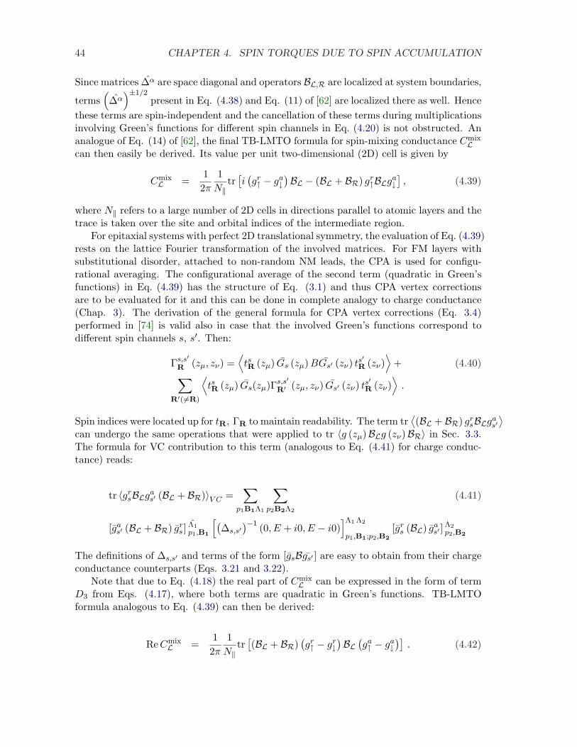
44 CHAPTER 4. SPIN TORQUES DUE TO SPIN ACCUMULATION
Since matrices ∆α are space diagonal and operators BL,R are localized at system boundaries,
terms(∆α
)±1/2present in Eq. (4.38) and Eq. (11) of [62] are localized there as well. Hence
these terms are spin-independent and the cancellation of these terms during multiplicationsinvolving Green’s functions for different spin channels in Eq. (4.20) is not obstructed. Ananalogue of Eq. (14) of [62], the final TB-LMTO formula for spin-mixing conductance Cmix
Lcan then easily be derived. Its value per unit two-dimensional (2D) cell is given by
CmixL =
12π
1N‖
tr[i(gr↑ − ga
↓)BL − (BL + BR) gr
↑BLga↓], (4.39)
where N‖ refers to a large number of 2D cells in directions parallel to atomic layers and thetrace is taken over the site and orbital indices of the intermediate region.
For epitaxial systems with perfect 2D translational symmetry, the evaluation of Eq. (4.39)rests on the lattice Fourier transformation of the involved matrices. For FM layers withsubstitutional disorder, attached to non-random NM leads, the CPA is used for configu-rational averaging. The configurational average of the second term (quadratic in Green’sfunctions) in Eq. (4.39) has the structure of Eq. (3.1) and thus CPA vertex correctionsare to be evaluated for it and this can be done in complete analogy to charge conductance(Chap. 3). The derivation of the general formula for CPA vertex corrections (Eq. 3.4)performed in [74] is valid also in case that the involved Green’s functions correspond todifferent spin channels s, s′. Then:
Γs,s′R (zµ, zν) =
⟨tsR (zµ) Gs (zµ)BGs′ (zν) ts
′R (zν)
⟩+ (4.40)
∑
R′(6=R)
⟨tsR (zµ) Gs(zµ)Γs,s′
R′ (zµ, zν) Gs′ (zν) ts′
R (zν)⟩.
Spin indices were located up for tR, ΓR to maintain readability. The term tr⟨(BL + BR) gr
sBLgas′⟩
can undergo the same operations that were applied to tr 〈g (zµ)BLg (zν)BR〉 in Sec. 3.3.The formula for VC contribution to this term (analogous to Eq. (4.41) for charge conduc-tance) reads:
tr 〈grsBLga
s′ (BL + BR)〉V C =∑
p1B1Λ1
∑
p2B2Λ2
(4.41)
[gas′ (BL + BR) gr
s ]Λ1p1,B1
[(∆s,s′
)−1 (0, E + i0, E − i0)]Λ1 Λ2
p1,B1;p2,B2
[grs (BL) ga
s′ ]Λ2p2,B2
The definitions of ∆s,s′ and terms of the form [gsBgs′ ] are easy to obtain from their chargeconductance counterparts (Eqs. 3.21 and 3.22).
Note that due to Eq. (4.18) the real part of CmixL can be expressed in the form of term
D3 from Eqs. (4.17), where both terms are quadratic in Green’s functions. TB-LMTOformula analogous to Eq. (4.39) can then be derived:
ReCmixL =
12π
1N‖
tr[(BL + BR)
(gr↑ − gr
↓)BL
(ga↑ − ga
↓)]. (4.42)
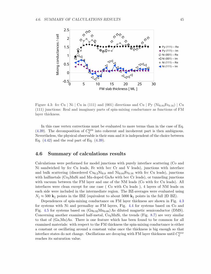
4.6. SUMMARY OF CALCULATIONS RESULTS 45
Figure 4.3: fcc Cu | Ni | Cu in (111) and (001) directions and Cu | Py (Ni0.84Fe0.16) | Cu(111) junctions: Real and imaginary parts of spin-mixing conductance as functions of FMlayer thickness.
In this case vertex corrections must be evaluated to more terms than in the case of Eq.(4.39). The decomposition of Cmix
L into coherent and incoherent part is then ambiguous.Nevertheless, the physical observable is their sum and it is independent of the choice betweenEq. (4.42) and the real part of Eq. (4.39).
4.6 Summary of calculations results
Calculations were performed for model junctions with purely interface scattering (Co andNi sandwiched by fcc Cu leads, Fe with bcc Cr and V leads), junctions with interfaceand bulk scattering (disordered Cu0.2Ni0.8 and Ni0.84Fe0.16 with fcc Cu leads), junctionswith halfmetals (Co2MnSi and Mn-doped GaAs with bcc Cr leads), or tunneling junctionswith vacuum between the FM layer and one of the NM leads (Co with fcc Cu leads). Allinterfaces were clean except for one case ( Co with Cu leads ), 4 layers of NM leads oneach side were included in the intermediate region. The BZ-averages were evaluated usingN‖ ≈ 500 k‖ points in the IBZ (equivalent to about 5000 k‖ points in the full 2D BZ).
Dependences of spin-mixing conductance on FM layer thickness are shown in Fig. 4.3for systems with Ni and permalloy as FM layers, Fig. 4.4 for systems based on Co andFig. 4.5 for systems based on (Ga0.92Mn0.08)As diluted magnetic semiconductor (DMS).Concerning another examined half-metal, Co2MnSi, the trends (Fig. 8.7) are very similarto that of (Ga,Mn)As. There is one feature which has been found to be common for allexamined materials: with respect to the FM thickness the spin-mixing conductance is eithera constant or oscillating around a constant value once the thickness is big enough so thatinterface states do not change. Oscillations are decaying with FM layer thickness until Cmix
Lreaches its saturation value.
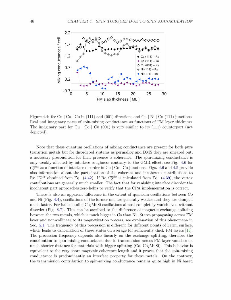
46 CHAPTER 4. SPIN TORQUES DUE TO SPIN ACCUMULATION
Figure 4.4: fcc Cu | Co | Cu in (111) and (001) directions and Cu | Ni | Cu (111) junctions:Real and imaginary parts of spin-mixing conductance as functions of FM layer thickness.The imaginary part for Cu | Co | Cu (001) is very similar to its (111) counterpart (notdepicted).
Note that these quantum oscillations of mixing conductance are present for both puretransition metals but for disordered systems as permalloy and DMS they are smeared out,a necessary precondition for their presence is coherence. The spin-mixing conductance isonly weakly affected by interface roughness contrary to the GMR effect, see Fig. 4.6 forCmixL as a function of interface disorder in Cu | Co | Cu junctions. Figs. 4.6 and 4.5 provide
also information about the participation of the coherent and incoherent contributions toRe Cmix
L obtained from Eq. (4.42). If Re CmixL is calculated from Eq. (4.39), the vertex
contributions are generally much smaller. The fact that for vanishing interface disorder theincoherent part approaches zero helps to verify that the CPA implementation is correct.
There is also an apparent difference in the extent of quantum oscillations between Coand Ni (Fig. 4.4), oscillations of the former one are generally weaker and they are dampedmuch faster. For half-metallic Co2MnSi oscillations almost completely vanish even withoutdisorder (Fig. 8.7). This can be ascribed to the difference of magnetic exchange splittingbetween the two metals, which is much bigger in Co than Ni. States propagating across FMlayer and non-collinear to its magnetization precess, see explanation of this phenomena inSec. 5.1. The frequency of this precession is different for different points of Fermi surface,which leads to cancellation of these states on average for sufficiently thick FM layers [15].The precession frequency depends also linearly on the exchange splitting, therefore thecontribution to spin-mixing conductance due to transmission across FM layer vanishes onmuch shorter distance for materials with bigger splitting (Co, Co2MnSi). This behavior isequivalent to the very short magnetic coherence length and it proves that the spin-mixingconductance is predominantly an interface property for these metals. On the contrary,the transmission contribution to spin-mixing conductance remains quite high in Ni based
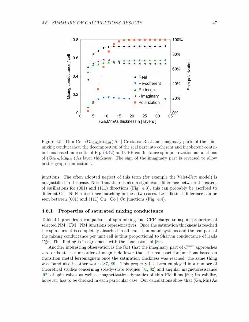
4.6. SUMMARY OF CALCULATIONS RESULTS 47
Figure 4.5: Thin Cr | (Ga0.92Mn0.08)As | Cr slabs: Real and imaginary parts of the spin-mixing conductance, the decomposition of the real part into coherent and incoherent contri-butions based on results of Eq. (4.42) and CPP conductance spin polarization as functionsof (Ga0.92Mn0.08)As layer thickness. The sign of the imaginary part is reversed to allowbetter graph composition.
junctions. The often adopted neglect of this term (for example the Valet-Fert model) isnot justified in this case. Note that there is also a significant difference between the extentof oscillations for (001) and (111) directions (Fig. 4.3), this can probably be ascribed todifferent Cu - Ni Fermi surface matching in these two cases. Less distinct difference can beseen between (001) and (111) Cu | Co | Cu junctions (Fig. 4.4).
4.6.1 Properties of saturated mixing conductance
Table 4.1 provides a comparison of spin-mixing and CPP charge transport properties ofselected NM | FM | NM junctions representatives. Once the saturation thickness is reachedthe spin current is completely absorbed in all transition metal systems and the real part ofthe mixing conductance per unit cell is thus proportional to Sharvin conductance of leadsCSh
N . This finding is in agreement with the conclusions of [89].Another interesting observation is the fact that the imaginary part of Cmix approaches
zero or is at least an order of magnitude lower than the real part for junctions based ontransition metal ferromagnets once the saturation thickness was reached; the same thingwas found also in other works [87, 89]. This property has been employed in a number oftheoretical studies concerning steady-state torques [81, 82] and angular magnetoresistance[92] of spin valves as well as magnetization dynamics of thin FM films [89]; its validity,however, has to be checked in each particular case. Our calculations show that (Ga,Mn)As
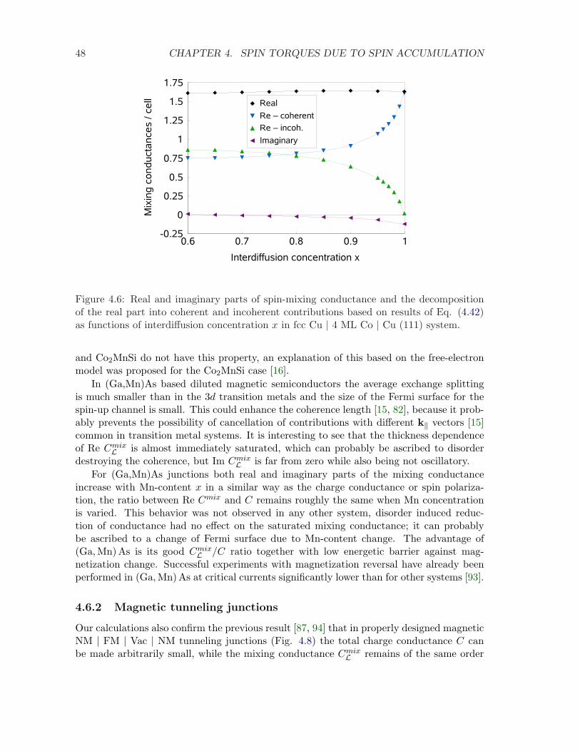
48 CHAPTER 4. SPIN TORQUES DUE TO SPIN ACCUMULATION
Figure 4.6: Real and imaginary parts of spin-mixing conductance and the decompositionof the real part into coherent and incoherent contributions based on results of Eq. (4.42)as functions of interdiffusion concentration x in fcc Cu | 4 ML Co | Cu (111) system.
and Co2MnSi do not have this property, an explanation of this based on the free-electronmodel was proposed for the Co2MnSi case [16].
In (Ga,Mn)As based diluted magnetic semiconductors the average exchange splittingis much smaller than in the 3d transition metals and the size of the Fermi surface for thespin-up channel is small. This could enhance the coherence length [15, 82], because it prob-ably prevents the possibility of cancellation of contributions with different k‖ vectors [15]common in transition metal systems. It is interesting to see that the thickness dependenceof Re Cmix
L is almost immediately saturated, which can probably be ascribed to disorderdestroying the coherence, but Im Cmix
L is far from zero while also being not oscillatory.For (Ga,Mn)As junctions both real and imaginary parts of the mixing conductance
increase with Mn-content x in a similar way as the charge conductance or spin polariza-tion, the ratio between Re Cmix and C remains roughly the same when Mn concentrationis varied. This behavior was not observed in any other system, disorder induced reduc-tion of conductance had no effect on the saturated mixing conductance; it can probablybe ascribed to a change of Fermi surface due to Mn-content change. The advantage of(Ga,Mn)As is its good Cmix
L /C ratio together with low energetic barrier against mag-netization change. Successful experiments with magnetization reversal have already beenperformed in (Ga,Mn)As at critical currents significantly lower than for other systems [93].
4.6.2 Magnetic tunneling junctions
Our calculations also confirm the previous result [87, 94] that in properly designed magneticNM | FM | Vac | NM tunneling junctions (Fig. 4.8) the total charge conductance C canbe made arbitrarily small, while the mixing conductance Cmix
L remains of the same order
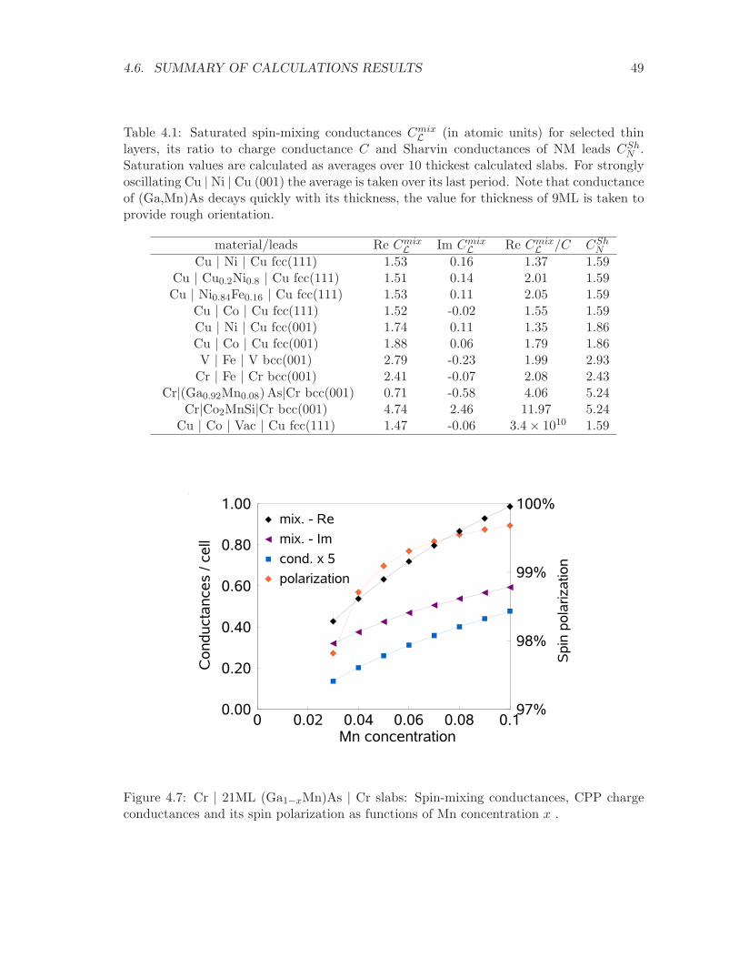
4.6. SUMMARY OF CALCULATIONS RESULTS 49
Table 4.1: Saturated spin-mixing conductances CmixL (in atomic units) for selected thin
layers, its ratio to charge conductance C and Sharvin conductances of NM leads CShN .
Saturation values are calculated as averages over 10 thickest calculated slabs. For stronglyoscillating Cu | Ni | Cu (001) the average is taken over its last period. Note that conductanceof (Ga,Mn)As decays quickly with its thickness, the value for thickness of 9ML is taken toprovide rough orientation.
material/leads Re CmixL Im Cmix
L Re CmixL /C CSh
N
Cu | Ni | Cu fcc(111) 1.53 0.16 1.37 1.59Cu | Cu0.2Ni0.8 | Cu fcc(111) 1.51 0.14 2.01 1.59Cu | Ni0.84Fe0.16 | Cu fcc(111) 1.53 0.11 2.05 1.59
Cu | Co | Cu fcc(111) 1.52 -0.02 1.55 1.59Cu | Ni | Cu fcc(001) 1.74 0.11 1.35 1.86Cu | Co | Cu fcc(001) 1.88 0.06 1.79 1.86V | Fe | V bcc(001) 2.79 -0.23 1.99 2.93
Cr | Fe | Cr bcc(001) 2.41 -0.07 2.08 2.43Cr|(Ga0.92Mn0.08)As|Cr bcc(001) 0.71 -0.58 4.06 5.24
Cr|Co2MnSi|Cr bcc(001) 4.74 2.46 11.97 5.24Cu | Co | Vac | Cu fcc(111) 1.47 -0.06 3.4× 10¹⁰ 1.59
Figure 4.7: Cr | 21ML (Ga1−xMn)As | Cr slabs: Spin-mixing conductances, CPP chargeconductances and its spin polarization as functions of Mn concentration x .
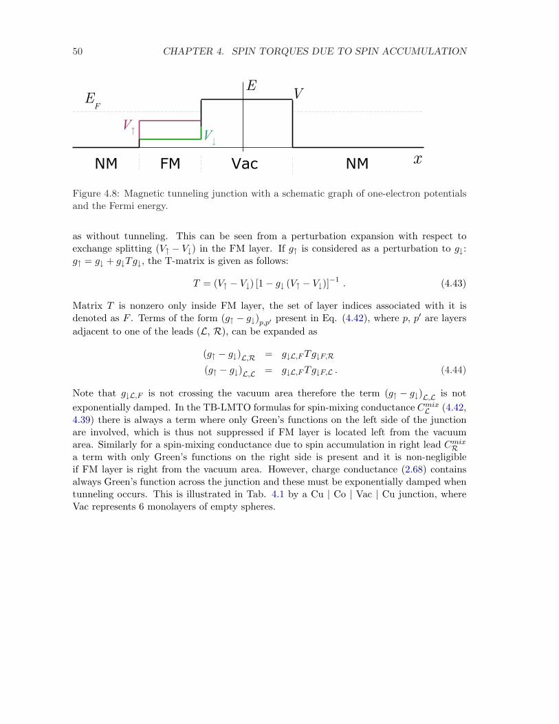
50 CHAPTER 4. SPIN TORQUES DUE TO SPIN ACCUMULATION
Figure 4.8: Magnetic tunneling junction with a schematic graph of one-electron potentialsand the Fermi energy.
as without tunneling. This can be seen from a perturbation expansion with respect toexchange splitting (V↑ − V↓) in the FM layer. If g↑ is considered as a perturbation to g↓:g↑ = g↓ + g↓Tg↓, the T-matrix is given as follows:
T = (V↑ − V↓) [1− g↓ (V↑ − V↓)]−1 . (4.43)
Matrix T is nonzero only inside FM layer, the set of layer indices associated with it isdenoted as F . Terms of the form (g↑ − g↓)p,p′ present in Eq. (4.42), where p, p′ are layersadjacent to one of the leads (L, R), can be expanded as
(g↑ − g↓)L,R = g↓L,FTg↓F,R(g↑ − g↓)L,L = g↓L,FTg↓F,L . (4.44)
Note that g↓L,F is not crossing the vacuum area therefore the term (g↑ − g↓)L,L is notexponentially damped. In the TB-LMTO formulas for spin-mixing conductance Cmix
L (4.42,4.39) there is always a term where only Green’s functions on the left side of the junctionare involved, which is thus not suppressed if FM layer is located left from the vacuumarea. Similarly for a spin-mixing conductance due to spin accumulation in right lead Cmix
Ra term with only Green’s functions on the right side is present and it is non-negligibleif FM layer is right from the vacuum area. However, charge conductance (2.68) containsalways Green’s function across the junction and these must be exponentially damped whentunneling occurs. This is illustrated in Tab. 4.1 by a Cu | Co | Vac | Cu junction, whereVac represents 6 monolayers of empty spheres.
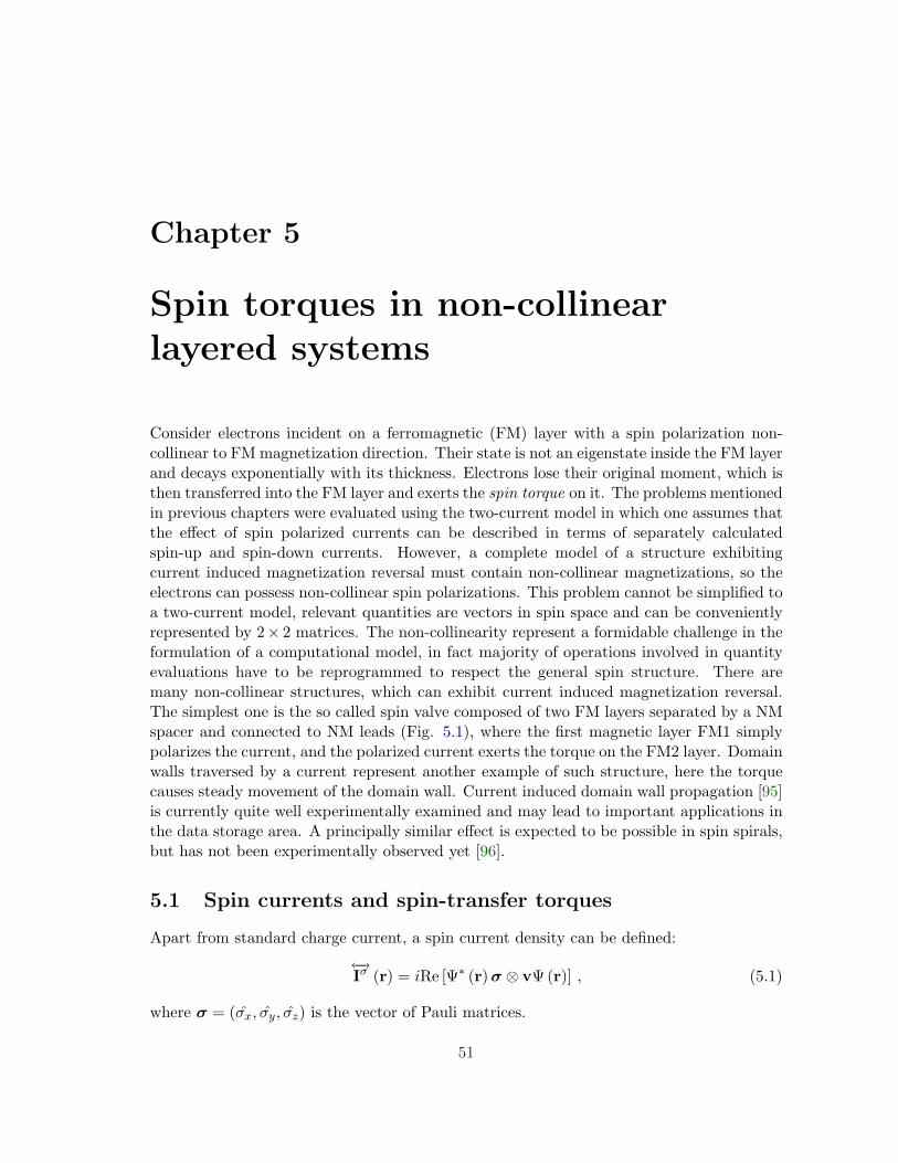
Chapter 5
Spin torques in non-collinearlayered systems
Consider electrons incident on a ferromagnetic (FM) layer with a spin polarization non-collinear to FM magnetization direction. Their state is not an eigenstate inside the FM layerand decays exponentially with its thickness. Electrons lose their original moment, which isthen transferred into the FM layer and exerts the spin torque on it. The problems mentionedin previous chapters were evaluated using the two-current model in which one assumes thatthe effect of spin polarized currents can be described in terms of separately calculatedspin-up and spin-down currents. However, a complete model of a structure exhibitingcurrent induced magnetization reversal must contain non-collinear magnetizations, so theelectrons can possess non-collinear spin polarizations. This problem cannot be simplified toa two-current model, relevant quantities are vectors in spin space and can be convenientlyrepresented by 2× 2 matrices. The non-collinearity represent a formidable challenge in theformulation of a computational model, in fact majority of operations involved in quantityevaluations have to be reprogrammed to respect the general spin structure. There aremany non-collinear structures, which can exhibit current induced magnetization reversal.The simplest one is the so called spin valve composed of two FM layers separated by a NMspacer and connected to NM leads (Fig. 5.1), where the first magnetic layer FM1 simplypolarizes the current, and the polarized current exerts the torque on the FM2 layer. Domainwalls traversed by a current represent another example of such structure, here the torquecauses steady movement of the domain wall. Current induced domain wall propagation [95]is currently quite well experimentally examined and may lead to important applications inthe data storage area. A principally similar effect is expected to be possible in spin spirals,but has not been experimentally observed yet [96].
5.1 Spin currents and spin-transfer torques
Apart from standard charge current, a spin current density can be defined:
←→Iσ (r) = iRe [Ψ∗ (r) σ ⊗ vΨ(r)] , (5.1)
where σ = (σx, σy, σz) is the vector of Pauli matrices.
51
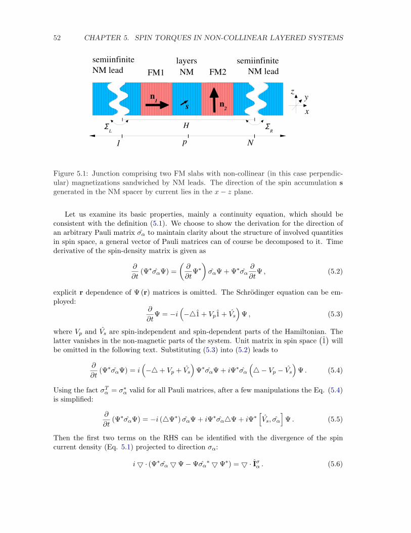
52 CHAPTER 5. SPIN TORQUES IN NON-COLLINEAR LAYERED SYSTEMS
Figure 5.1: Junction comprising two FM slabs with non-collinear (in this case perpendic-ular) magnetizations sandwiched by NM leads. The direction of the spin accumulation sgenerated in the NM spacer by current lies in the x− z plane.
Let us examine its basic properties, mainly a continuity equation, which should beconsistent with the definition (5.1). We choose to show the derivation for the direction ofan arbitrary Pauli matrix σα to maintain clarity about the structure of involved quantitiesin spin space, a general vector of Pauli matrices can of course be decomposed to it. Timederivative of the spin-density matrix is given as
∂
∂t(Ψ∗σαΨ) =
(∂
∂tΨ∗
)σαΨ + Ψ∗σα
∂
∂tΨ , (5.2)
explicit r dependence of Ψ (r) matrices is omitted. The Schrodinger equation can be em-ployed:
∂
∂tΨ = −i
(−41 + Vp1 + Vs
)Ψ , (5.3)
where Vp and Vs are spin-independent and spin-dependent parts of the Hamiltonian. Thelatter vanishes in the non-magnetic parts of the system. Unit matrix in spin space
(1)
willbe omitted in the following text. Substituting (5.3) into (5.2) leads to
∂
∂t(Ψ∗σαΨ) = i
(−4+ Vp + Vs
)Ψ∗σαΨ + iΨ∗σα
(4− Vp − Vs
)Ψ . (5.4)
Using the fact σTα = σ∗α valid for all Pauli matrices, after a few manipulations the Eq. (5.4)
is simplified:
∂
∂t(Ψ∗σαΨ) = −i (4Ψ∗) σαΨ + iΨ∗σα4Ψ + iΨ∗
[Vs, σα
]Ψ . (5.5)
Then the first two terms on the RHS can be identified with the divergence of the spincurrent density (Eq. 5.1) projected to direction σα:
i5 · (Ψ∗σα 5Ψ−Ψσα∗ 5Ψ∗) = 5 · Iσ
α . (5.6)
5.1. SPIN CURRENTS AND SPIN-TRANSFER TORQUES 53
Contrary to the charge conductance the continuity equation contains an additional termiΨ∗
[Vs, σα
]Ψ, in vector formulation iΨ∗
[Vs,σ
]Ψ. As was already pointed out [84], spin
is generally not conserved and the additional term corresponds to an influence of a spin-split potential. For the potential given by a magnetic exchange field B, the term readsi [B · σ,σ] = 2B × σ due to the Pauli matrix algebra. This term perpendicular to boththe magnetic field and the spin density is apparently similar to the precession term presentin the Landau-Lifshitz-Gilbert equation. In a ferromagnet, where the field B correspondsto its exchange field, this spin-precession term contains averages over many states withdifferent Larmor frequencies, which leads to a quick relaxation of terms in the spin-densitymatrix non-collinear to the magnetization n in the ferromagnet [86]. However presenceof these terms due to divergence of spin current also twists the magnetization of the FMlayer and the effective field B, the absorbed spin is transferred to the lattice magnetizationgiving rise to spin-transfer torque τ . These processes have to be studied in more detailwhen the dynamics of spin-transfer torque generated rotation is examined, here we restrictonly to evaluation of torque τ acting to a FM layer with prescribed uniform magnetizationdirection n and not its further evolution. A discussion about how the spin-transfer torqueis balanced by the torque exerted by the effective magnetic field and the relations valid forthe spin-current divergence in a steady state can be seen in [97].
The mechanism of the spin-precession term leads to the quick decay of spin currentcomponent perpendicular to the magnetization direction n of FM layer [15] so that thecurrent leaving the sufficiently thick FM layer is polarized parallel to n. Note that thecomponent parallel to the magnetization can be understood completely within the two-current model (with no non-collinearity taken into account), it can be only reflected ortransmitted as it is unaffected by the spin-precession term. The spin-precession term isperpendicular to n and the torque τ is too. In order to find τ it is natural to evaluatespin currents in NM regions adjacent to the FM region. The spin-precession term is zerothere (without the spin-orbit coupling), hence spin current is conserved and its value doesnot depend on a position inside the NM region. A deviation from the equilibrium (non-polarized) spin density called spin accumulation (Sec. 4.1) may arise there because of spincurrents and it is not destroyed as in FM layer. Spin-transfer torque acting on a subsequentFM layer can alternatively be related directly to it.
The additional source term in continuity equation is also denoted as angular spin currentand this kind of continuity equation is analogous to a flow of a classical vector [98]. If spin-orbit coupling is included in Vs and thus participates in the angular spin current, it becomesparticularly important to postulate a better definition of the spin current so that it remainsconserved [99]. Within fully relativistic treatment a suitable generalization of spin densityhas been discovered, leading to a new definition of spin current; spin-transfer torque due tospin-orbit coupling has been examined in this framework [100]. Recently a relation betweenthe electrical polarization and the antisymmetric components of the spin current has beenfound based on fully relativistic theory [101], which allowed to propose a way to measurespin-current directly and thus help experimental characterization of the spin-transfer torquephenomena.
54 CHAPTER 5. SPIN TORQUES IN NON-COLLINEAR LAYERED SYSTEMS
5.2 Ab initio formulation
In LMTO approach system’s spin-dependent properties are incorporated in the potentialfunction P . In the non-collinear situation these are general matrices in spin space P . Inthe local reference frame associated with its magnetization direction its matrix P (0) isdiagonal in spin space:
P (0) =(P ↑ 00 P↓
). (5.7)
Its representation in the global reference frame is obtained using a rotation matrix in spinspace, assuming rotation by angle ϑ in the x− z plane:
Rϑ =(
cos ϑ2 − sin ϑ
2
sin ϑ2 cos ϑ
2
), P (ϑ) = RϑP (0) Rϑ
+(5.8)
In principle, self-consistent DFT calculation of electronic structure should be also per-formed in spin space, leading to an exact knowledge of Green’s functions direction in spinspace. Our aim here is not to examine systems with complicated non-collinear bulk mag-netic structure but only non-collinear arrangement of separated magnetically homogeneouslayers. This problem can be replaced within reasonable accuracy by a DFT solution of acorresponding collinear system, parts of its ground state solution corresponding to magneticlayers are then rotated in spin space by means of Eq. (5.8) to attain the desired angle.This is justified by the theory leading to the frozen potential approximation [102]. Dif-ferently speaking we assume that the ground state of one magnetic layer is not influencedby a change of magnetization direction of another magnetic layer. It also implicates thatthe magnetic structure of material is assumed completely known and prescribed initially,deviations from it that would minimize the total energy cannot be found this way, this isthe same as for two-current model solutions.
5.2.1 Spin currents from linear response theory
As we have shown spin torques acting on FM layers of a magnetic multilayer are closelyrelated to spin currents flowing through the structure. These are not conserved in non-collinear systems, hence the point of their evaluation must be properly chosen. The spincurrent operator at a given point r is defined as
Jσ (r) = −i[X (r) ,H]σ . (5.9)
Its linear response to external potential applied at the leads is evaluated (Sec. 2.4), welabel it spin conductance Cσ. For the corresponding spin-torque response we use the termtorkance Cτ . One should first check whether the spin conductance fulfills the conditions(2.54) that allow the general linear response formula to reduce to the canonical form (2.43).For this purpose we choose the axis system so that both magnetization directions lie in thex−z plane and the response direction first coincides with the x axis (the in-plane response).Hence the Hamiltonian reads
H = H0 +Wxσx +Wzσz , (5.10)
5.2. AB INITIO FORMULATION 55
where H0 represents the spin-independent part of the Hamiltonian and Wx, Wz are com-ponents of the exchange splitting. The explicit dependence of H0, Wx,z and X on positionis omitted for simplicity. The response operator is
A‖ = −i[X, H
]σx = −i [X,H0σx +Wx + iWzσy] . (5.11)
Note that both operators X and Wx, Wzσy are diagonal in real space, Wzσy is non-diagonalin spin space, but X is a unit matrix there, hence their commutator is always zero. Theoperator B corresponds to an external electrostatic potential ϕ (r). Only the trivial choiceU = 1 = U−1 satisfies the condition for the Hamiltonian (first Eq. of 2.54). ObviouslyBT = B, hence ε = 1. For the operator A‖ = −i [X,H0σx] it follows:
−AT‖ = −i [X,H0σx] (5.12)
The last condition in (2.54) is therefore satisfied. A similar derivation for A‖z = −[X, H]σz
leads to the same conclusion, but for the out-of-plane response A⊥ = −i[X, H]σy thecondition (2.54) cannot be satisfied, hence all terms in Eq. (2.51) need to be evaluated.Generally a linear combination of Pauli matrices after the commutator in A should fulfillthe same condition as the Hamiltonian, and therefore we restrict the calculation to in-planecomponents. Now the general spin current operator (5.9) is substituted into Eq. (2.43)with the assumption of zero temperature:
Cσ (EF ) = − 1π
Tr
Im Gr (EF ) [X,H] σIm Gr (EF ) [φ,H]. (5.13)
5.2.2 TB-LMTO expression
Eq. (5.13) is expressed in the LMTO formulation in a way analogous to that for chargeconductance [65]. Note that a transformation to a particular LMTO representation corre-sponding to its TB form is desirable, and one should find a formulation of (5.13) independentof representation. We follow the way adopted in [62] for charge conductance. All potentialparameters (Sec. 2.2.1) are diagonal in space, but now they are general matrices in spinspace. Note that the tight-binding Hamiltonian (see Eq. (8) of [62]) therefore contains
terms(∆α
Rl
)1/2SRL,R′L′ (z)
(∆α
Rl
)1/2off-diagonal in real space, which are now non-trivial
in spin space within exchange-split areas, and the commutator[X, H
]may possibly void
the last condition in (2.54). However, consistently with statements in Sec. 5.1 we chooseto evaluate spin currents only in NM areas, the operator X is then replaced by a projectorΠN−N to (yet unspecified) continuous set of layers terminated at NM areas. The commu-tator
[ΠN−N , H
]is non-zero only inside NM areas, where H reduces to the form of H0 and
the argumentation of the preceding subsection applies.
For the first-order accuracy, we note that GR,R′ (z) =(∆α
)−1/2
Rgα
R,R′ (z)(∆α
)−1/2
R′remains valid regardless of the spin structure of the involved matrices. These matricesare multiplied by current operators localized at NM areas, hence the only involved spatial
parts of matrices(∆α
)−1/2are also unitary in spin space, so that they commute with σ.
56 CHAPTER 5. SPIN TORQUES IN NON-COLLINEAR LAYERED SYSTEMS
They can then be canceled with(∆α
)1/2in the transformed current operator (Eq. (10) of
Ref. [62]). Spin conductance formula for non-collinear situations in TB-LMTO is thereforeanalogous to Eq. (2.59), note that commutators of an operator diagonal in space with Hcan be replaced by commutators with S :
CσN−N (EF ) = − 2
πTr Im gr,α (EF ) [ΠN−N , S
α] σIm gr,α (EF ) [φ, Sα] . (5.14)
For the second-order accuracy, the derivation presented in Section III B of [62] holds also forpotential parameters given as matrices in spin space. Current operators are again nonzero
only in NM regions and σ commutes there with the term(∆
)−1/21 + Sα (α− γ) present
in the second-order current operator (Eq. (28) of Ref. [62]). Hence it can be shifted so thatit is adjacent to [Πp, S
α] and the resulting formula (5.14) is correct up to the second orderin energy expansion ε = E − Eν . The LMTO representation index and energy argumentwill be omitted from now on.
In order to find the torkances Cτ2 acting on the monitored magnetic slab (FM2) in a
spin valve structure we need to express the spin conductances Cσ in NM areas on bothsides of FM2. One side can correspond to an end of the structure, we choose the rightlead (labeled R), the opposite side is always inside the NM layer between two FM layersand one its layers is chosen and labeled p (Fig. 5.1). The choice of the projector ΠN−N
to be restricted to layers between p and R leads directly to torkance evaluation. Term[ΠN−N , S
α] is nonzero only at the edges of this area, calculation of Eq. (5.14) at thesetwo points separately corresponds to an evaluation of spin conductances at layers p and N(adjacent to R): Cσ
p and CσR . The torkance acting on the second FM layer is then given
byCτ
2 = CσR −Cσ
p , (5.15)
in agreement with the presented statements about the spin current continuity (Sec. 5.1).Equation (5.14) can be evaluated using Eq. (2.60) as in Sec. 2.4.1. Equation (2.64) can
be utilized only for the commutator [φ, S], this yields:
Cτ2 = − 1
2πTrBgr [ΠN−N , S] σgrB(ϕga − gaϕ) . (5.16)
Using the assumption of field source in the left lead (Bϕ = ϕB = BL) and performingsubstitution (2.60) backwards leads to the following formula:
Cτ2 =
i
2πTr [ΠN−N , S]σgrBLga − [ΠN−N , S]σgaBLgr . (5.17)
Spin conductance at the right lead (CσR) corresponds to the flux between layers N and
N + 1:
CσR =
i
2πTrSN,N+1σg
rN+1,1BLga
1,N − SN+1,NσgrN,1BLga
1,N+1 −SN,N+1σg
aN+1,1BLgr
1,N + SN+1,NσgaN,1BLgr
1,N+1 . (5.18)
Employing identities (A16) of [65] leads to a compact formula in the Caroli-like form [64].The final result is that for the charge conductance (2.68) multiplied by the vector of Pauli
5.2. AB INITIO FORMULATION 57
matrices:CσR (zµ, zν) =
12π
Tr gN,1 (zµ)BLg1,N (zν)BRσ . (5.19)
Note that CσR (E + i0, E − i0) 6= Cσ
R (E − i0, E + i0) since σy 6= σyT . Charge conductance
formula for non-collinear situations is obtained from Eq. (5.19) by substitution of σ by aunity matrix in spin space. Note that due to the current conservation it is independent ofposition, but the most convenient choice is to evaluate it at layer N adjacent to the rightlead as in Eq. (5.19).
Spin conductance at the opposite side corresponds to the flux between layers p and p+1,its expression is analogous to Eq. (5.18), where N is replaced by p. This quantity cannotbe reduced to more simple form like Eq. (5.19). The final formula for spin conductance atlayer p:
Cσp (zµ, zν) =
i
2πTr BL (g1,p (zµ)Sp,p+1σgp+1,1 (zν)− g1,p+1 (zµ)Sp+1,pσgp,1 (zν)) .
(5.20)
5.2.3 Ab initio torkance in non-collinear spin valves
For a non-collinear NM | FM1 | NM | FM2 | NM system there is another approach leadingvery quickly to a torkance formula, limited also to its in-plane part. Note that the torqueacting on each FM layer is perpendicular to its magnetization direction as discussed inSec. 5.1. Therefore the in-plane component of the torque acting on layer FM2 τ2‖ is fullydetermined by the projection of τ2 to the magnetization direction n1:
∣∣τ2‖∣∣ = τ2 ·n1/ sinϑ,
where ϑ is an angle between n1 and n2. Also note that this projection equals the projectionof the total torque τ acting on the spin valve, because for FM1 it also holds τ1 ⊥ n1 :
τ2‖ · n1 = τ · n1 . (5.21)
The fact that the total torkance can be used instead of a partial one significantly simplifiesthe calculation. We perform the derivation in NEGF formalism here, similar to the one per-formed in Sec. 4.2. Operator τ can be chosen as the examined response operator, the sameas in the spin-mixing conductance derivation, and the only physically reasonable quantity,its projection τ · n1, is then extracted immediately. In contrast to the assumptions of Sec.4.2, the perturbation of the Hamiltonian is now due to external electrostatic potential andthus not spin-polarized, the non-collinear spin structure is incorporated into system Green’sfunctions. The first order change of self-energy is then
δΣ<L = f ′ (E)BLδφL . (5.22)
Substitution of Eqs. (5.23, 4.9, 5.22) into Eq. (4.8) and use of the fact that [σ,BL] = 0allows to obtain Cτ
2‖, the linear response coefficient for τ2‖ given by the final formula:
Cτ2‖ sinϑ =
12π
Tr (n1 · σ) [i (Gr −Ga)BL −GrBLGaB]
=12π
Tr (n1 · σ) [GrBRGaBL −GrBLGaBR] (5.23)
58 CHAPTER 5. SPIN TORQUES IN NON-COLLINEAR LAYERED SYSTEMS
In contrast to the derivation of Cτ2 , Eq. (5.15) the whole formula can be expressed in
the Caroli-like form as charge conductance does. For the situation with external potentialacting on the opposite side (R) of the system the torkance is found to be:
CτR2‖ sinϑ =
12π
Tr (n1 · σ) [GrBLGaBR −GrBRGaBL] , (5.24)
which is the exact opposite of Eq. (5.23). This way a crucial feature of current inducedmagnetization reversal is directly obtained: current direction reversal causes also torquedirection reversal [91], which has been already observed in experiments [103] and is in factused to recognize current induced magnetization switching from other phenomena. We havefound that total torque in system is exactly antisymmetric with respect to current directionin agreement with [91], its in-plane component exerted on one of FM layers is then alsoantisymmetric due to relation (5.21).
Transformation of formula (5.23) to the TB-LMTO formulation is straightforward:
Cτ2‖ sinϑ =
12π
Tr(n1 · σ)
[gr
1,NBRgaN,1BL − gr
1,NBLgaN,1BR
]. (5.25)
5.3 Comparison to spin-mixing conductance
We have presented another calculation of spin torques in Chapter 4. Now an obviousquestion arises, what is the relation of its results to the results of the theory presentedhere. The first one provides spin torques as a response to the spin accumulation, while thesecond one relates it directly to the electrostatic potential difference (similarly to the well-known charge conductance) of a more complicated structure where the spin accumulationis generated internally. We first verify whether the spin currents present due to the spinaccumulation lead to the same spin torque as the approach described in Chap. 4 based onthe spin-mixing conductance.
We again examine the NM | FM | NM junction, the spin currents on the two sides ofthe FM layer can then be defined as
JL = −i[ΠL,H0]σ = −i[ΠLσ,H],JR = −i[ΠR, H0]σ = −i[ΠRσ,H], (5.26)
where the kinetic energy (intersite hopping) is contained in the spin-independent part H0
of the Hamiltonian H, Eq. (4.1), and where the ΠL and ΠR denote projection operators onthe two NM leads including a few adjacent (non-magnetic) layers of the intermediate regionsuch that ΠLγ = ΠRγ = 0. The spin accumulation (δEL) again acts as an infinitesimalperturbation to the lesser self-energy Σ< (Eq. 4.10), the linear response coefficients for thespin currents are defined as
KLL =
δJLδEL
, KRL =
δJRδEL
. (5.27)
Their direct evaluation reveals that because of the similar arrangement of Pauli matricesthey can be obtained by the same approach as in the section 4.2 for the response coefficient
5.3. COMPARISON TO SPIN-MIXING CONDUCTANCE 59
CL, Eq. (4.12). The explicit expressions are given by
KLL =
12π
Tr [i(σGr −Gaσ)(σ · a)BL − σBLGr(σ · a)BLGa] ,
KRL = − 1
2πTr [σBRGr(σ · a)BLGa] , (5.28)
where several simple properties of the projectors, such as [ΠL,Σr,a(E)] = 0 and ΠLB = BL(and similarly for ΠR), were used. Note that KL
L + KRL = CL which reflects the above
mentioned relation between the torque and the spin currents.The resulting formulas can be summarized as
KLL = 2 ReCL,mix
L n× (a× n) + 2 ImCL,mixL a× n + (C↑ + C↓)(n · a)n,
KRL = 2 ReCR,mix
L n× (a× n) + 2 ImCR,mixL a× n− (C↑ + C↓)(n · a)n, (5.29)
where we introduced complex coefficients in analogy to the spin-mixing conductance, Eq. (4.20),namely
CL,mixL =
12π
tr[i(Gr↑ −Ga
↓)BL − BLGr
↑BLGa↓],
CR,mixL = − 1
2πtr
(BRGr↑BLGa
↓). (5.30)
Two comments to these results are now in order. First, the dependence of the spin currentson the orientation of the spin accumulation (s) and the magnetization (n), Eq. (5.29), ismore complicated than that of the spin torque, Eq. (4.19). Second, an obvious relationCmixL = CL,mix
L +CR,mixL can be proved from Eqs. (4.20, 5.30). However, this decomposition
does not justify a direct interpretation of the quantities CL,mixL and CR,mix
L as respectivecontributions to the total spin-mixing conductance due to the left and right spin currents,since the latter contain also terms proportional to the total charge conductance C↑ + C↓and parallel to the magnetization direction n, see Eq. (5.29). Hence, the quantities CL,mix
Land CR,mix
L refer only to the transverse components of the left and right spin currents withrespect to the exchange field of the FM layer.
In the scattering theory analogy, we can show that Eq. (4.37) can be decomposed toits left and right contributions due to the transverse spin currents , Eq. (5.30) in the sameway as Cmix
L is decomposed:
CL,mixL =
12π
(1− r↑r∗↓
), CR,mix
L = − 12πt↑t∗↓ (5.31)
We have shown that evaluations of the spin torque from the change of “spin conduc-tances due to spin accumulation” KL and from the spin-mixing conductance are in factequivalent methods, in agreement with the continuity equation for spin currents (5.5). Notethat our non-collinear methods provide only the in-plane component of the torque, whilefrom the mixing conductance method in-plane (real part) and out-of-plane (imaginary part)components are obtained. In principle, if the spin accumulation generated in given structurewas known, the spin-mixing conductance should give the spin-torque as well as Eq. (5.23).Hence the results of Eq. (5.23) contain in addition to spin-mixing conductance information
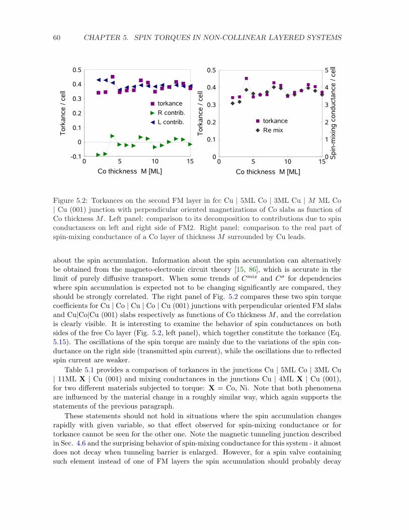
60 CHAPTER 5. SPIN TORQUES IN NON-COLLINEAR LAYERED SYSTEMS
Figure 5.2: Torkances on the second FM layer in fcc Cu | 5ML Co | 3ML Cu | M ML Co| Cu (001) junction with perpendicular oriented magnetizations of Co slabs as function ofCo thickness M . Left panel: comparison to its decomposition to contributions due to spinconductances on left and right side of FM2. Right panel: comparison to the real part ofspin-mixing conductance of a Co layer of thickness M surrounded by Cu leads.
about the spin accumulation. Information about the spin accumulation can alternativelybe obtained from the magneto-electronic circuit theory [15, 86], which is accurate in thelimit of purely diffusive transport. When some trends of Cmix and Cσ for dependencieswhere spin accumulation is expected not to be changing significantly are compared, theyshould be strongly correlated. The right panel of Fig. 5.2 compares these two spin torquecoefficients for Cu | Co | Cu | Co | Cu (001) junctions with perpendicular oriented FM slabsand Cu|Co|Cu (001) slabs respectively as functions of Co thickness M , and the correlationis clearly visible. It is interesting to examine the behavior of spin conductances on bothsides of the free Co layer (Fig. 5.2, left panel), which together constitute the torkance (Eq.5.15). The oscillations of the spin torque are mainly due to the variations of the spin con-ductance on the right side (transmitted spin current), while the oscillations due to reflectedspin current are weaker.
Table 5.1 provides a comparison of torkances in the junctions Cu | 5ML Co | 3ML Cu| 11ML X | Cu (001) and mixing conductances in the junctions Cu | 4ML X | Cu (001),for two different materials subjected to torque: X = Co, Ni. Note that both phenomenaare influenced by the material change in a roughly similar way, which again supports thestatements of the previous paragraph.
These statements should not hold in situations where the spin accumulation changesrapidly with given variable, so that effect observed for spin-mixing conductance or fortorkance cannot be seen for the other one. Note the magnetic tunneling junction describedin Sec. 4.6 and the surprising behavior of spin-mixing conductance for this system - it almostdoes not decay when tunneling barrier is enlarged. However, for a spin valve containingsuch element instead of one of FM layers the spin accumulation should probably decay
5.4. SUMMARY OF CALCULATIONS RESULTS 61
Table 5.1: Torkances in junctions Cu | 5ML Co | 3ML Cu | 11ML X | Cu (001) andcorresponding mixing conductances in junctions Cu | 11ML X | Cu (001), for two differentmaterials subjected to torque: X = Co, Ni. Ratio between Co and Ni results for both thesequantities.
System Cτ2‖ Re
(CmixL + Cmix
R)
Ratio Co/NiCu | 5ML Co | 3ML Cu | 11ML Co | Cu 0.37 1.28Cu | 5ML Co | 3ML Cu | 11ML Ni | Cu 0.29
Cu | 11ML Co | Cu 3.59 1.38Cu | 11ML Ni | Cu 2.61
exponentially similar to the charge conductance and so the torkance should. This agreeswith our results and it is also supported by the observation that while the formula (4.42) forspin-mixing conductance contains Green’s function elements avoiding the tunnel barrier,only those going through it are present in (5.23). Nevertheless, this fact does not mean thatthe design of such junction lacks any application potential, but it must be updated so thatenough spin accumulation is generated by an additional current going in other direction,as was proposed in [87].
5.4 Summary of calculations results
Non-collinear transport calculation was implemented only for systems with no substitutionaldisorder. All calculations were performed for NM | FM1 | NM | FM2 | NM model spin valves.First we briefly review few important general properties of obtained results. All theseproperties are expected to be fulfilled if there is no fundamental error in the implementationor formulation of torkance calculation:
• Our calculations have shown perfect agreement between torkances Cτ2‖ obtained from
(5.23) and a projection of Cτ2 from (5.15) to the magnetization direction n1, which
also corroborates the equivalence of the NEGF and Kubo based derivation here.
• The antisymmetry with respect to current direction found as a consequence of thetheory developed for Cτ
2‖ was also verified by means of Cτ2 obtained from (5.15). All
torkance results will from now on be therefore labeled as Cτ2‖ without specifying the
method.
• We verified that charge conductance is invariant with respect to an arbitrary rotationof the whole system in spin space.
• For parallel and antiparallel orientations of FM layers torkance vanish.
• Spin conductances are independent of the measurement position within one NM layer.
• The component of torkance Cτ2 parallel to the magnetization of the FM2 layer vanish,
and for torkance Cτ1 the same is valid concerning the direction parallel to FM1 layer.
62 CHAPTER 5. SPIN TORQUES IN NON-COLLINEAR LAYERED SYSTEMS
Table 5.2: Torkances Cτ2‖ and total charge conductances C in junctions Cu | 4ML X | 4ML
Cu | 4ML Ni | Cu (001) for X=Co,Ni and Cu | 4ML Fe | 4ML Cu | 4ML Fe | Cu (001)with perpendicular magnetizations of FM layers, spin polarization of conductance via Cu |X | Cu and Cr | Fe | Cr junctions, and the ratio of Cτ
2‖ to it.
System Cτ2‖ C FM1 Pol Cτ
2‖/C/PolCu | 4ML Co | 4ML Cu | 4ML Ni | Cu (001) 0.38 0.97 31% 1.26Cu | 4ML Ni | 4ML Cu | 4ML Ni | Cu (001) 0.092 1.23 7.2% 1.07Cr | 4ML Fe | 4ML Cr | 4ML Fe | Cr (001) −0.36 0.81 −46% 0.97
• Spin currents at the NM layer preceding the FM1 layer are polarized mostly in thedirection of FM1, while those at NM layer after the FM2 layer are polarized in thedirection of FM2, which is consistent with the statements on decaying perpendicularspin current component in Sec. 5.1.
Ab initio formulation of torkance allows to examine the role of FM1, FM2 and NM spacermaterials, their thicknesses and the angle ϑ between the two FM layers. The dependenceon the switching layer FM2 should be in rough agreement with the information on it fromthe spin-mixing conductance as is discussed in the preceding section. The polarizing layerFM1 determines the torkance exerted on FM2 mainly by the amount how much does itpolarize the current passing through it, this is supported by findings presented in Tab.5.2. Note that even though torkance differs between systems with Co and Ni as FM1 slabsignificantly (cca. four times), its ratio to spin polarization of a standalone NM | FM1 |NM junction is very similar. There are slight changes of the ratio caused mainly by thedifference between spin polarization in the NM | FM1 | NM junction alone and accompaniedby another perpendicularly oriented magnetic slab (FM2). The two FM slabs cannot ofcourse be accurately seen as independent with their effect on spin current summed, that isan idea within the series resistor model (see Sec. 2.3).
This finding about the dependence on FM1 slab polarization also proposes the way toreverse torque direction: Use systems where conductance is polarized opposite to magneti-zation of FM1, this idea was already realized experimentally [104]. Negative spin polariza-tion (also referred to as negative spin asymmetry) may arise due to scattering propertiesof particular interfaces with NM metal or due to bulk scattering properties of FM layerinfluenced suitably by a strong disorder. The latter case is not accessible currently for ournon-collinear calculation, but one such system is examined in Sec. 6.4 with respect to itsmagnetoresistance, which is also impacted. The former case corresponds for example to Fe| Cr (001) interface. This interface prefers minority electrons (with respect to Fe magneti-zation) and the overall (referred to as net) spin polarization of Cr | Fe | Cr conductance isnegative even though standalone Fe layer of course contains more conducting channels formajority electrons, an experimental verification of this fact can be seen in [105]. Inversionof torque direction for this system is clearly obtained from our calculations (Tab. 5.2). Notethat spin torque exerted on FM2 layer can be reversed by having negative spin anisotropycorresponding to layer FM1, but not layer FM2.
5.4. SUMMARY OF CALCULATIONS RESULTS 63
5.4.1 Angular dependence
Dependences of the total resistance and spin-transfer torque on the FM1 and FM2 rela-tive angle ϑ are one of the most interesting problems to be solved for non-collinear systems.Analytical formulas for these dependencies have been proposed based on experimental find-ings and justified theoretically [15, 106] for spin valves with identical FM layers within anassumption that electrons’ phase coherence is lost between interfaces (semiclassical approx-imation):
R (ϑ)−R (0)R (π)−R (0)
=1− cos (ϑ)
χ (1 + cos (ϑ)) + 2(5.32)
Cτ2‖ (ϑ) =
CP
8πω
sin (ϑ)1 + ω − (1− ω) cos (ϑ)
, (5.33)
where
χ =1
1− P 2ω − 1 , ω =
∣∣Cmix∣∣2
C.ReCmix, (5.34)
and spin polarization P , mixing and charge conductances Cmix, C are properties of one ofNM/FM/NM junctions.
Torkances and resistances of a Cu | Co | Cu | Co | Cu junction are depicted in Fig. 5.2.We calculate coefficients χ, ω and compare results from (5.32,5.33) to our results in thesame Figure, Cτ
2‖ (ϑ) is multiplied by a constant to best accommodate extent of Cτ2‖. Note
that the agreement between approximate formulas (5.32,5.33) and our more accurate abinitio calculations is quite good, especially the angular position of the spin torque extreme.However, the small almost saddle of angular dependence left from the torque maximum isnot caught by the simple formula (5.33).
With increasing spin polarization the value of χ grows and with increasing Cmix/C bothω and χ grows. This supports the asymmetry of Eq. (5.33) so that its peak angle ϑm isshifted towards ϑ = π. This prediction is in overall agreement with our results (Tab. 5.3),but some additional subtle phenomena not accounted for in Eq. (5.33) may shift the peakposition about ±0.1π. Therefore we rather compare the ratio between the absolute valuesof torque angular derivatives at angles ϑ = 0, π, which should also describe the angularasymmetry:
η =∂∂ϑ C
τ2‖ (ϑ = 0)
∂∂ϑ C
τ2‖ (ϑ = π)
. (5.35)
Results of this comparison are provided in Tab. 5.3 for selected junctions. A completeangular dependence of a pure half-metal can be seen in Sec. 8.8.
The asymmetry of torkance angular distribution can be understood from examining theasymmetry of spin accumulation in NM spacer, which is commonly higher for situationscloser to antiparallel orientation. However if the spin valve is constructed from such ma-terials, that its NM | FM1 | NM part has negative and NM | FM2 | NM part positive netspin polarization (or vice versa), antiparallel alignment of the layers is more conducting,which corresponds to the negative GMR (Sec. 6.4.2). Spin accumulation is then higher forparallel alignment and the torque angular asymmetry is reversed, this is illustrated in Tab.5.3 for Cr | Fe | Cr | Co2MnSi | Cr system.
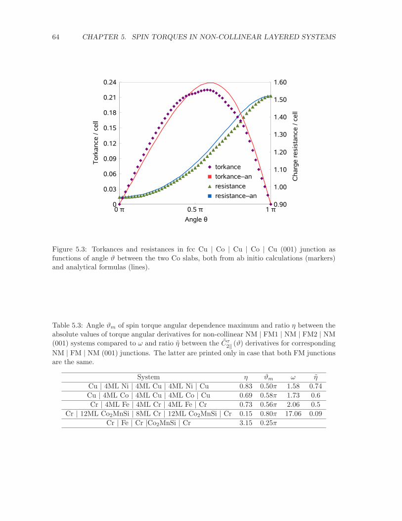
64 CHAPTER 5. SPIN TORQUES IN NON-COLLINEAR LAYERED SYSTEMS
Figure 5.3: Torkances and resistances in fcc Cu | Co | Cu | Co | Cu (001) junction asfunctions of angle ϑ between the two Co slabs, both from ab initio calculations (markers)and analytical formulas (lines).
Table 5.3: Angle ϑm of spin torque angular dependence maximum and ratio η between theabsolute values of torque angular derivatives for non-collinear NM | FM1 | NM | FM2 | NM(001) systems compared to ω and ratio η between the Cτ
2‖ (ϑ) derivatives for correspondingNM | FM | NM (001) junctions. The latter are printed only in case that both FM junctionsare the same.
System η ϑm ω η
Cu | 4ML Ni | 4ML Cu | 4ML Ni | Cu 0.83 0.50π 1.58 0.74Cu | 4ML Co | 4ML Cu | 4ML Co | Cu 0.69 0.58π 1.73 0.6Cr | 4ML Fe | 4ML Cr | 4ML Fe | Cr 0.73 0.56π 2.06 0.5
Cr | 12ML Co2MnSi | 8ML Cr | 12ML Co2MnSi | Cr 0.15 0.80π 17.06 0.09Cr | Fe | Cr |Co2MnSi | Cr 3.15 0.25π
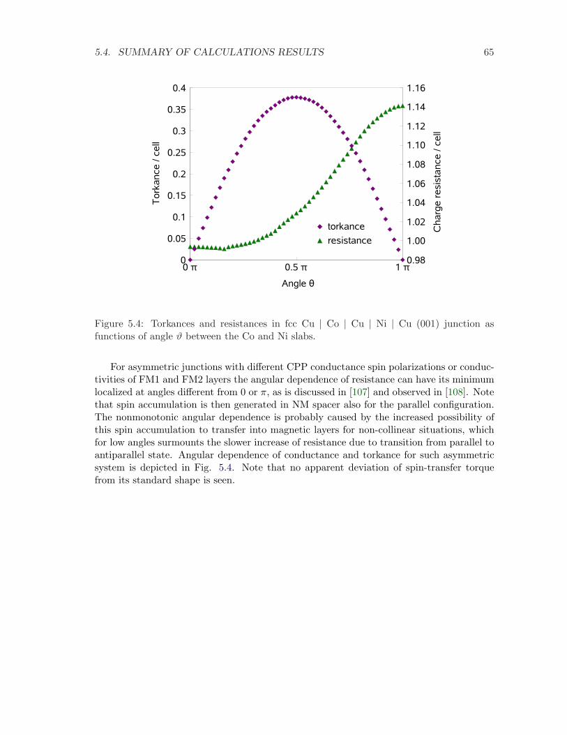
5.4. SUMMARY OF CALCULATIONS RESULTS 65
Figure 5.4: Torkances and resistances in fcc Cu | Co | Cu | Ni | Cu (001) junction asfunctions of angle ϑ between the Co and Ni slabs.
For asymmetric junctions with different CPP conductance spin polarizations or conduc-tivities of FM1 and FM2 layers the angular dependence of resistance can have its minimumlocalized at angles different from 0 or π, as is discussed in [107] and observed in [108]. Notethat spin accumulation is then generated in NM spacer also for the parallel configuration.The nonmonotonic angular dependence is probably caused by the increased possibility ofthis spin accumulation to transfer into magnetic layers for non-collinear situations, whichfor low angles surmounts the slower increase of resistance due to transition from parallel toantiparallel state. Angular dependence of conductance and torkance for such asymmetricsystem is depicted in Fig. 5.4. Note that no apparent deviation of spin-transfer torquefrom its standard shape is seen.

66 CHAPTER 5. SPIN TORQUES IN NON-COLLINEAR LAYERED SYSTEMS
Chapter 6
Co/Cu based multilayers withsubstitutional disorder
GMR effect in Co/Cu based multilayers has been observed [109] recently after the initialGMR experiments on Fe/Cr multilayers done by Baibich et al. in 1988[2]. Productionof Co/Cu metallic multilayers is well developed and they exhibit a reasonable GMR ratioeven at room temperature, while having lower coercivity fields than Fe/Cr. Moreover Curepresents a truly nonmagnetic spacer in contrast to the complicated magnetic structureof Cr. From the theoretical point of view they are based on quite simple transition metalswith no significant relativistic contribution, whose electronic structure and other calculationpredictions are in good agreement with experiments. Therefore they represent an idealmaterial to test the validity of presented theories before going to more complicated systems,that may show an even more interesting physical behavior.
6.1 Electronic structure
The self-consistency of one-electron potentials was achieved in intermediate regions com-prising also a few (3-5) monolayers of the attached metallic leads. One principal layer (Sec.2.2.3) was formed by one atomic layer for fcc(111) stacking while two neighboring atomiclayers per principal layer were necessary in fcc(001) and bcc(001) cases. The integrationsover the 2D BZ were performed on a uniform mesh of about 1000 k‖ points to determinethe electronic structure.
The key to understand the origin of high magnetoresistance in metallic multilayersis the band structure for energies near the Fermi energy. It is well known that there isa very good matching between the band structures of Cu and Co↑, while Cu and Co↓exhibit a band mismatch. The calculated band structures of these two materials depictedin Fig. 6.1 demonstrate this behavior, which is the source of the high spin polarization ofelectron scattering at their interfaces leading to GMR phenomena calculated in subsequentsections. Systems with the 2D translational symmetry must in reality be described by theBloch spectral function which contains peaks of finite width instead of δ-functions, hencethe simple band structure picture is inaccurate, but an assumption of bulk-like atoms in themultilayer is sufficient for a qualitative understanding of the multilayer’s spin-dependent
67
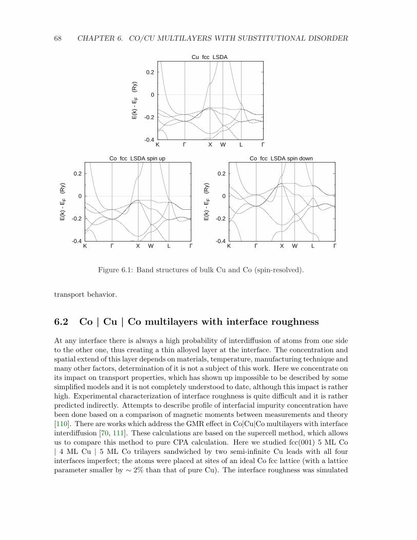
68 CHAPTER 6. CO/CU MULTILAYERS WITH SUBSTITUTIONAL DISORDER
-0.4
-0.2
0
0.2
E(k
) -
EF
(Ry)
Cu fcc LSDA
K Γ X W L Γ
-0.4
-0.2
0
0.2
E(k
) -
EF
(Ry)
Co fcc LSDA spin up
K Γ X W L Γ-0.4
-0.2
0
0.2
E(k
) -
EF
(Ry)
Co fcc LSDA spin down
K Γ X W L Γ
Figure 6.1: Band structures of bulk Cu and Co (spin-resolved).
transport behavior.
6.2 Co | Cu | Co multilayers with interface roughness
At any interface there is always a high probability of interdiffusion of atoms from one sideto the other one, thus creating a thin alloyed layer at the interface. The concentration andspatial extend of this layer depends on materials, temperature, manufacturing technique andmany other factors, determination of it is not a subject of this work. Here we concentrate onits impact on transport properties, which has shown up impossible to be described by somesimplified models and it is not completely understood to date, although this impact is ratherhigh. Experimental characterization of interface roughness is quite difficult and it is ratherpredicted indirectly. Attempts to describe profile of interfacial impurity concentration havebeen done based on a comparison of magnetic moments between measurements and theory[110]. There are works which address the GMR effect in Co|Cu|Co multilayers with interfaceinterdiffusion [70, 111]. These calculations are based on the supercell method, which allowsus to compare this method to pure CPA calculation. Here we studied fcc(001) 5 ML Co| 4 ML Cu | 5 ML Co trilayers sandwiched by two semi-infinite Cu leads with all fourinterfaces imperfect; the atoms were placed at sites of an ideal Co fcc lattice (with a latticeparameter smaller by ∼ 2% than that of pure Cu). The interface roughness was simulated
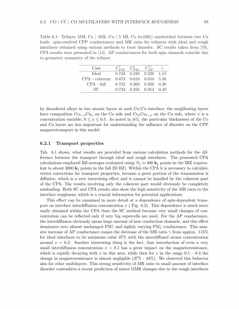
6.2. CO | CU | CO MULTILAYERS WITH INTERFACE ROUGHNESS 69
Table 6.1: Trilayer 5ML Co | 4ML Cu | 5 ML Co fcc(001) sandwiched between two Culeads: spin-resolved CPP conductances and MR ratio for trilayers with ideal and roughinterfaces obtained using various methods to treat disorder. SC results taken from [70],CPA results were presented in [14]. AP conductances for both spin channels coincide dueto geometric symmetry of the trilayer.
Case C↑PM C↓PM C↑↓AP γ
Ideal 0.743 0.238 0.228 1.15CPA - coherent 0.673 0.016 0.054 5.38
CPA - full 0.722 0.260 0.356 0.38SC 0.733 0.256 0.354 0.40
by disordered alloys in two atomic layers at each Co/Cu interface; the neighboring layershave composition Co1−xCux on the Co side and CoxCu1−x on the Cu side, where x is aconcentration variable, 0 ≤ x ≤ 0.5. As noted in [65], the particular thicknesses of the Coand Cu layers are less important for understanding the influence of disorder on the CPPmagnetotransport in this model.
6.2.1 Transport properties
Tab. 6.1 shows, what results are provided from various calculation methods for the dif-ference between the transport through ideal and rough interfaces. The presented CPAcalculations employed BZ-averages evaluated using N‖ ≈ 400 k‖ points in the IBZ (equiva-lent to about 3000 k‖ points in the full 2D BZ). Within the CPA it is necessary to calculatevertex corrections for transport properties, because a great portion of the transmission isdiffusive, which is a very interesting effect and it cannot be handled by the coherent partof the CPA. The results involving only the coherent part would obviously be completelymisleading. Both SC and CPA results also show the high sensitivity of the MR ratio to theinterface roughness, which is a crucial information for potential applications.
This effect can be examined in more detail at a dependence of spin-dependent trans-port on interface interdiffusion concentration x ( Fig. 6.2). This dependence is much moreeasily obtained within the CPA than the SC method because very small changes of con-centration can be reflected only if very big supercells are used. For the AP conductance,the interdiffusion obviously opens large amount of new conduction channels, and this effectdominates over almost unchanged PM↑ and sightly varying PM↓ conductance. This mas-sive increase of AP conductance causes the decrease of the MR ratio γ from approx. 115%for ideal interfaces to its minimum value 37% with the interdiffused atoms concentrationaround x = 0.2. Another interesting thing is the fact, that introduction of even a verysmall interdiffusion concentration x < 0.1 has a great impact on the magnetoresistance,which is rapidly decaying with x in this area, while then for x in the range 0.1 − 0.4 thechange in magnetoresistance is almost negligible (37% - 43%). We observed this behavioralso for other multilayers. This strong sensitivity of MR ratio to small amount of interfacedisorder contradicts a recent prediction of minor GMR changes due to the rough interfaces
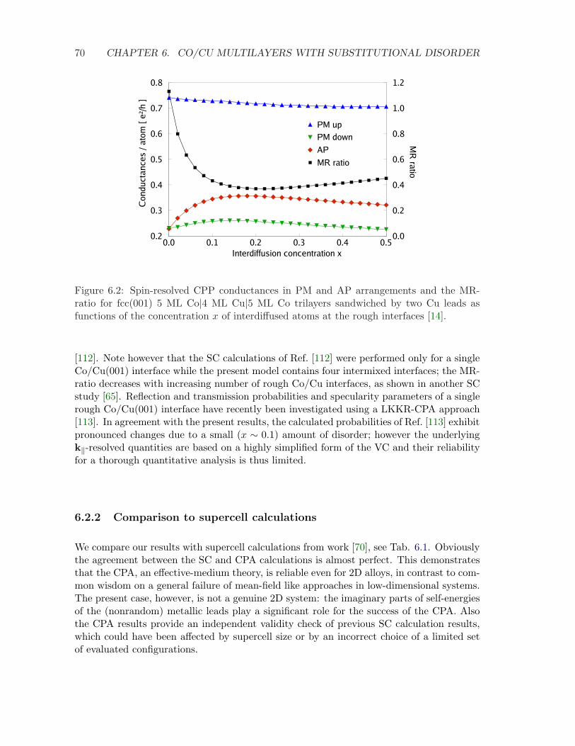
70 CHAPTER 6. CO/CU MULTILAYERS WITH SUBSTITUTIONAL DISORDER
Figure 6.2: Spin-resolved CPP conductances in PM and AP arrangements and the MR-ratio for fcc(001) 5 ML Co|4 ML Cu|5 ML Co trilayers sandwiched by two Cu leads asfunctions of the concentration x of interdiffused atoms at the rough interfaces [14].
[112]. Note however that the SC calculations of Ref. [112] were performed only for a singleCo/Cu(001) interface while the present model contains four intermixed interfaces; the MR-ratio decreases with increasing number of rough Co/Cu interfaces, as shown in another SCstudy [65]. Reflection and transmission probabilities and specularity parameters of a singlerough Co/Cu(001) interface have recently been investigated using a LKKR-CPA approach[113]. In agreement with the present results, the calculated probabilities of Ref. [113] exhibitpronounced changes due to a small (x ∼ 0.1) amount of disorder; however the underlyingk‖-resolved quantities are based on a highly simplified form of the VC and their reliabilityfor a thorough quantitative analysis is thus limited.
6.2.2 Comparison to supercell calculations
We compare our results with supercell calculations from work [70], see Tab. 6.1. Obviouslythe agreement between the SC and CPA calculations is almost perfect. This demonstratesthat the CPA, an effective-medium theory, is reliable even for 2D alloys, in contrast to com-mon wisdom on a general failure of mean-field like approaches in low-dimensional systems.The present case, however, is not a genuine 2D system: the imaginary parts of self-energiesof the (nonrandom) metallic leads play a significant role for the success of the CPA. Alsothe CPA results provide an independent validity check of previous SC calculation results,which could have been affected by supercell size or by an incorrect choice of a limited setof evaluated configurations.
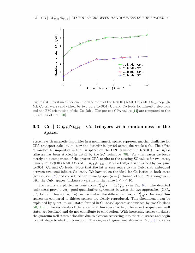
6.3. CO | CU0.84NI0.16 | CO TRILAYERS WITH RANDOMNESS IN THE SPACER 71
Figure 6.3: Resistances per one interface atom of the fcc(001) 5 ML Co|s ML Cu0.84Ni0.16|5ML Co trilayers sandwiched by two pure fcc(001) Cu and Co leads for minority electronsand the FM orientation of the Co slabs. The present CPA values [14] are compared to theSC results of Ref. [70].
6.3 Co | Cu0.84Ni0.16 | Co trilayers with randomness in thespacer
Systems with magnetic impurities in a nonmagnetic spacer represent another challenge forCPA transport calculation, now the disorder is spread across the whole slab. The effectof random Ni impurities in the Cu spacer on the CPP transport in fcc(001) Co/Cu/Cotrilayers has been studied in detail by the SC technique [70]. For this reason we focusmerely on a comparison of the present CPA results to the existing SC values for two cases,namely for fcc(001) 5 ML Co|s ML Cu0.84Ni0.16|5 ML Co trilayers sandwiched by two purefcc(001) Cu and Co leads. Note that the latter case refers to the CuNi slab embeddedbetween two semi-infinite Co leads. We have taken the ideal fcc Co lattice in both cases(see Section 6.2) and considered the minority spin (σ = ↓) channel of the FM arrangementwith the CuNi spacer thickness s varying in the range 1 ≤ s ≤ 10.
The results are plotted as resistances R↓FM(s) = 1/C↓FM(s) in Fig. 6.3. The depictedresistances prove a very good quantitative agreement between the two approaches (CPA,SC) for both leads (Cu, Co); in particular, the different slopes of R↓FM(s) for very thinspacers as compared to thicker spacers are clearly reproduced. This phenomenon can beexplained by quantum-well states formed in Cu-based spacers sandwiched by two Co slabs[70, 114]. The resistivity of the alloy in a thin spacer is high, because the quantum wellstates are localized and do not contribute to conduction. With increasing spacer thicknessthe quantum well states delocalize due to electron scattering into other k‖ states and beginto contribute to electron transport. The degree of agreement shown in Fig. 6.3 indicates
72 CHAPTER 6. CO/CU MULTILAYERS WITH SUBSTITUTIONAL DISORDER
Figure 6.4: MR-ratio for fcc(111) trilayersM ML Co0.8Cr0.2|20 ML Cu|2 ML Co sandwichedby two Cu leads calculated by the present CPA approach [14] and the SC technique ofRef. [115] as functions of the CoCr slab thickness M . The experimental values of Ref. [105]refer to Co0.8Cr0.2|Cu|Co|Cu multilayers.
that the localized nature of the quantum-well states does not represent a principal obstaclefor applicability of the CPA.
6.4 CoCr | Cu | Co trilayers exhibiting negative GMR
Recently, several various F1|Cu|Co|Cu fcc(111) multilayers containing a random binaryferromagnetic alloy F1 have been manufactured that exhibit a transition from a positiveto negative GMR effect with increasing thickness M of the ferromagnetic alloy [105]. Thenegative GMR corresponds to a situation when the AP state is more conducting than thePM one. The value of M where the transition occurs is called a compensation thicknessMt. The experimental observation has been explained theoretically for Co0.8Cr0.2|Cu|Cotrilayers using the SC method [115].
6.4.1 Transport properties
Here the CPA transport calculation is compared to the SC approach [115], both for fcc(111)trilayers M ML Co0.8Cr0.2|20 ML Cu|2 ML Co, where the Co0.8Cr0.2 layer thickness coversan interval 2 ≤M ≤ 20, sandwiched by two semi-infinite Cu leads (all atoms placed on theideal fcc Co lattice). This replaces the experimental setup of 20x repeated F1|Cu|Co|Cu
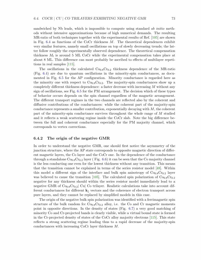
6.4. COCR | CU | CO TRILAYERS EXHIBITING NEGATIVE GMR 73
sandwiched by Nb leads, which is impossible to compute using standard ab initio meth-ods without intensive approximations because of high numerical demands. The resultingMR-ratio of both techniques together with the experimental results of Ref. [105] are shownin Fig. 6.4 as functions of the CoCr thickness M . The theoretical dependences exhibitvery similar features, namely small oscillations on top of slowly decreasing trends; the lat-ter follow roughly the experimentally observed dependence. The theoretical compensationthickness Mt is around 5 ML CoCr while the experimental compensation takes place atabout 8 ML. This difference can most probably be ascribed to effects of multilayer repeti-tions in real samples [115].
The oscillations in the calculated Co0.8Cr0.2 thickness dependence of the MR-ratio(Fig. 6.4) are due to quantum oscillations in the minority-spin conductances, as docu-mented in Fig. 6.5 for the AP configuration. Minority conductance is regarded here asthe minority one with respect to Co0.8Cr0.2. The majority-spin conductances show up acompletely different thickness dependence: a faster decrease with increasing M without anysign of oscillations, see Fig. 6.5 for the PM arrangement. The decision which of these typesof behavior occurs depends on the spin channel regardless of the magnetic arrangement.The different transport regimes in the two channels are reflected also by the coherent anddiffusive contributions of the conductances: while the coherent part of the majority-spinconductance represents a smaller contribution, exponentially decaying withM , the coherentpart of the minority-spin conductance survives throughout the whole range of M studiedand it reflects a weak scattering regime inside the CoCr slab. Note the big difference be-tween the full and coherent conductance especially for the PM majority channel, whichcorresponds to vertex corrections.
6.4.2 The origin of the negative GMR
In order to understand the negative GMR, one should first notice the asymmetry of thejunction structure, where the AP state corresponds to opposite magnetic direction of differ-ent magnetic layers, the Co layer and the CoCr one. In the dependence of the conductancethrough a standalone Co0.8Cr0.2 layer ( Fig. 6.6) it can be seen that the Co majority channelis the less conducting one even for the lowest thickness without any transition. This meansthat the transition cannot be explained in terms of the series resistor model [48]. Withinthis model a different sign of the interface and bulk spin anisotropy of Co0.8Cr0.2 layerwas believed to cause the transition [105]. The calculated spin polarization of Co0.8Cr0.2
negative for any thickness should within the series resistor model immediately lead to anegative GMR of Co0.8Cr0.2| Cu| Co trilayer. Realistic calculations take into account dif-ferent conductances for different k‖ vectors and the coherence of electron transport acrosspure layers, and they cannot be replaced by simplified models in this case.
The origin of the negative bulk spin polarization was identified with a ferrimagnetic spinstructure of the bulk random fcc Co0.8Cr0.2 alloy, i.e. the Co and Cr magnetic momentspoint in opposite directions. In the density of states (Fig. 6.7) a very good matching ofminority Co and Cr-projected bands is clearly visible, while a virtual bound state is formedin the Cr-projected density of states of the CoCr alloy majority electrons [115]. This statereflects a strong scattering regime leading thus to a rapid decrease of the majority-spinconductances with increasing CoCr layer thickness M .
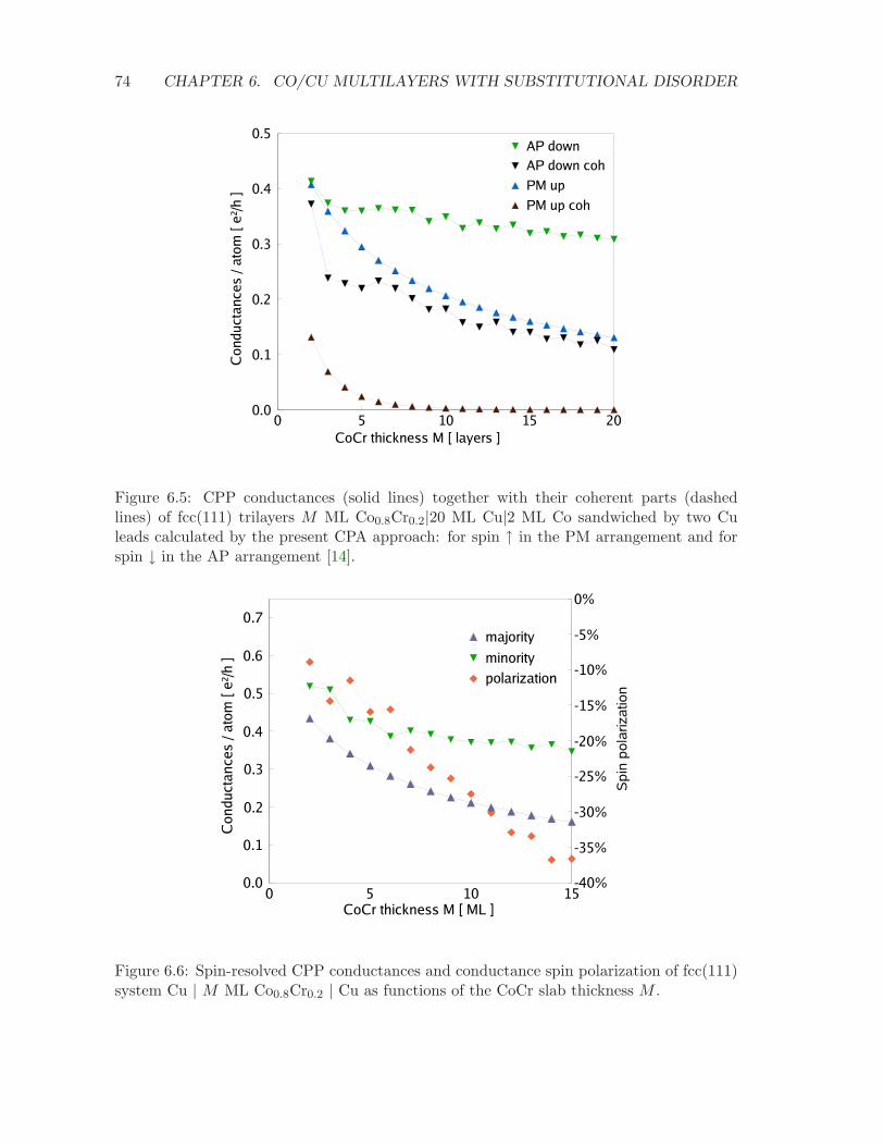
74 CHAPTER 6. CO/CU MULTILAYERS WITH SUBSTITUTIONAL DISORDER
Figure 6.5: CPP conductances (solid lines) together with their coherent parts (dashedlines) of fcc(111) trilayers M ML Co0.8Cr0.2|20 ML Cu|2 ML Co sandwiched by two Culeads calculated by the present CPA approach: for spin ↑ in the PM arrangement and forspin ↓ in the AP arrangement [14].
Figure 6.6: Spin-resolved CPP conductances and conductance spin polarization of fcc(111)system Cu | M ML Co0.8Cr0.2 | Cu as functions of the CoCr slab thickness M .
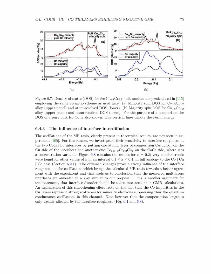
6.4. COCR | CU | CO TRILAYERS EXHIBITING NEGATIVE GMR 75
(a) (b)
Figure 6.7: Density of states (DOS) for fcc Co0.8Cr0.2 bulk random alloy calculated in [115]employing the same ab initio scheme as used here. (a) Minority spin DOS for Co0.8Cr0.2
alloy (upper panel) and atom-resolved DOS (lower). (b) Majority spin DOS for Co0.8Cr0.2
alloy (upper panel) and atom-resolved DOS (lower). For the purpose of a comparison theDOS of a pure bulk fcc-Co is also shown. The vertical lines denote the Fermi energy.
6.4.3 The influence of interface interdiffusion
The oscillations of the MR-ratio, clearly present in theoretical results, are not seen in ex-periment [105]. For this reason, we investigated their sensitivity to interface roughness atthe two CoCr/Cu interfaces by putting one atomic layer of composition Cu1−xCox on theCu side of the interfaces and another one Co0.8−xCr0.2Cux on the CoCr side, where x isa concentration variable. Figure 6.8 contains the results for x = 0.2; very similar trendswere found for other values of x in an interval 0.1 ≤ x ≤ 0.4, in full analogy to the Co | Cu| Co case (Section 6.2.1). The obtained changes prove a strong influence of the interfaceroughness on the oscillations which brings the calculated MR-ratio towards a better agree-ment with the experiment and that leads us to conclusion, that the measured multilayersinterfaces are annealed in a way similar to our proposal. This is another argument forthe statement, that interface disorder should be taken into account in GMR calculations.An explanation of this smoothening effect rests on the fact that the Co impurities in theCu layers represent strong scatterers for minority electrons suppressing thus the quantumconductance oscillations in this channel. Note however that the compensation length isonly weakly affected by the interface roughness (Fig. 6.4 and 6.8).
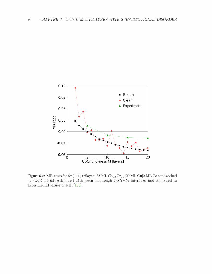
76 CHAPTER 6. CO/CU MULTILAYERS WITH SUBSTITUTIONAL DISORDER
Figure 6.8: MR-ratio for fcc(111) trilayersM ML Co0.8Cr0.2|20 ML Cu|2 ML Co sandwichedby two Cu leads calculated with clean and rough CoCr/Cu interfaces and compared toexperimental values of Ref. [105].
Chapter 7
(Ga,Mn)As thin layers
The successful doping of GaAs with Mn has been realized for the first time in 1996 by H.Ohno [116], giving rise to (Ga,Mn)As, an important representative of the diluted magneticsemiconductors (DMS). The III-V DMS like, e.g., Mn-doped GaAs, GaN, and InAs withMn atoms substituting the cations, represent nowadays the most frequently studied DMSsystems [25]. The first III-V DMS (In,Mn)As was grown by molecular beam epitaxy in1989 [117], subsequently the same group discovered hole-mediated ferromagnetism in thiscompound [118]. Holes are introduced into the system by the replacement of Ga or In byMn and the hole-mediated ferromagnetism attracts ongoing interest [119]. The change inparent semiconductor caused by doping can be understood as a kind of the metal-insulatortransition [68].
General feature of these systems is the random distribution of a small concentrationof transition metal atoms as for example Mn on the cation sublattice. Due to the smallconcentrations these systems behave structurally as semiconductors and can be easily grownon their corresponding parent substrate, i.e. (Ga,Mn)As on GaAs. Moreover they can bedoped and manipulated as semiconductors and they are half-metals[119–123], which bothoffers a large prospect for applications. However a problem of these DMS systems is thattheir Curie temperatures are well below room temperature because of their main property,the low concentration of magnetic atoms. This is the major obstacle for applications,hence a strong effort is targeted towards its resolution, and new representatives of DMS oralready known ones prepared in other ways are currently exhibiting still higher, althoughyet insufficient Curie temperatures.
DMS represent system with a complicated interplay of various physical phenomena[25]. Some of its properties appear to be described or explained satisfactorily only by abinitio calculations. The detailed theory including, e.g., magnetic interactions and Curietemperature evaluation [124], the role of effects of spin-orbit coupling, remains far beyondthe scope of this work. Here we concentrate mainly on its zero temperature transportproperties and on an inclusion of properties that can influence it. Thin layers of (Ga,Mn)Asor similar material may provide features useful for many spintronics applications. High spinpolarization of electron transport is a crucial property for these applications.
77
78 CHAPTER 7. (GA,MN)AS THIN LAYERS
Figure 7.1: (Ga,Mn)As structure
7.1 Bulk (Ga,Mn)As
In order to explore thin layer properties, it is desirable to first understand its bulk coun-terpart complex behavior. Existing theoretical studies include first-principles calculationsof the exchange interactions and the Curie temperatures [123–126]. The theoretical studiesof transport properties of these systems, on the other hand, remain confined to a modellevel [127, 128]. It has been shown in a recent experiment [129] that controlled annealingof thin (Ga,Mn)As films accompanied by monitoring the resistivity during growth can leadto high Curie temperatures of the films. Moreover, a pronounced correlation between theCurie temperatures and the conductivities of the real samples has been reported [129].
The structure of (Ga,Mn)As is shown in Fig. 7.1. In the presented calculations, emptyspheres in tetrahedral interstitial positions of the zinc-blende lattice were employed forreasons of a good space filling and equal Wigner-Seitz radii for all atoms and empty sphereswere used. The valence basis comprised s-, p-, and d-type orbitals, where the Ga 3d orbitalswere put into the core, which improves the calculation estimate of the band gap width (1.3eV) and the valence-band width (6.8 eV). The Mn atoms were placed randomly on thecation sublattice. Electronic structure calculations reveal a band gap on the Fermi levelin the minority DOS (Fig. 7.2), thus the system acts as an half-metal: an insulator forminority spin electrons and a metal for majority ones.
Bulk transport properties were in detail examined by TB-LMTO and CPA methods in[130]. Residual resistivities as functions of Mn-content x are depicted in Fig. 7.3. Theircalculated values for a typical Mn-content x = 5% lie in the range 1 − 5 × 10⁻⁵ Ωm (seebelow), in good agreement with experiment [129, 131]. Note that the vertex part of the
7.1. BULK (GA,MN)AS 79
20
15
10
5
0
5
10
15
20
-0.6 -0.4 -0.2 0 0.2
DO
S (
stat
es/s
pin/
Ry)
E - EF (Ry)
maj.
min.
tot.
Mn (x 0.5)
-0.2 -0.1 0 0.1 0.2 0.3 0.4
Blo
ch s
pect
ral f
unct
ion
E - EF (Ry)
maj.
min.
Figure 7.2: (Ga,Mn)As: density of states with highlighted local DOS on Mn atom, and theBloch spectral function at the Γ point.
conductivity is very small in this case. We observe the decrease of the resistivity withconcentration of Mn-impurities, which is just an opposite dependence to that known formetallic alloys. The reason for such behavior is a competition of two trends in the DMS’s:
(i) the increase of ρ with increasing concentration of defects which is due to impurityscattering, and
(ii) the increase of the conductivity, i.e., the decrease of ρ, with increasing number ofcarriers which is in turn proportional to the concentration of Mn atoms.
The second effect is obviously dominant in the examined range of Mn concentration.Such a strong dependence on the number of carriers is missing in typical metallic alloyswith a large number of carriers at the Fermi energy only weakly depending on the alloycomposition. In agreement with the prediction from the density of states, the minority spincomponent of conductance is zero.
7.1.1 Lattice defects
Real samples of (Ga,Mn)As tend to contain lattice defects, namely As antisites on the Gasublattice (AsGa, concentration y) and Mn interstitials (Mni, concentration z), both actas double donors [122]. These defects reduce the Curie temperature [123] and influencea number of ground-state properties including the lattice parameter [132]. This fact canalso be used to estimate the actual amount of lattice defects from X-ray lattice parametermeasurements. DFT calculations [132] have shown that the lattice constant dependenceon impurity concentrations can be approximated as linear (Fig. 7.4), dependences on each
80 CHAPTER 7. (GA,MN)AS THIN LAYERS
Figure 7.3: Residual resistivity of the (Ga1−x−yMnxAsy)As alloy as a function of the Mn-content [130]: without As-antisites (y = 0, squares) and with 1% As-antisites (y = 0.01,triangles). The open and full symbols refer to the coherent and the total conductivities,respectively.
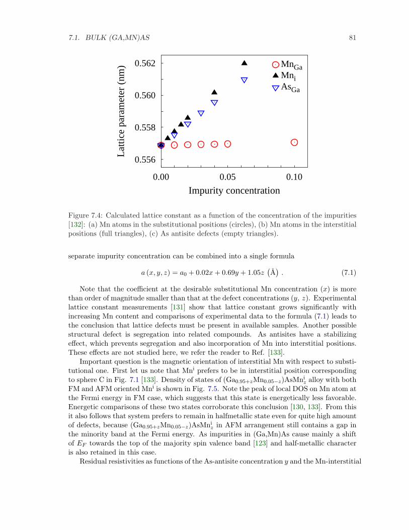
7.1. BULK (GA,MN)AS 81
0.556
0.558
0.560
0.562
0.00 0.05 0.10
Lat
tice
para
met
er (
nm)
Impurity concentration
MnGaMniAsGa
Figure 7.4: Calculated lattice constant as a function of the concentration of the impurities[132]: (a) Mn atoms in the substitutional positions (circles), (b) Mn atoms in the interstitialpositions (full triangles), (c) As antisite defects (empty triangles).
separate impurity concentration can be combined into a single formula
a (x, y, z) = a0 + 0.02x+ 0.69y + 1.05z(A
). (7.1)
Note that the coefficient at the desirable substitutional Mn concentration (x) is morethan order of magnitude smaller than that at the defect concentrations (y, z). Experimentallattice constant measurements [131] show that lattice constant grows significantly withincreasing Mn content and comparisons of experimental data to the formula (7.1) leads tothe conclusion that lattice defects must be present in available samples. Another possiblestructural defect is segregation into related compounds. As antisites have a stabilizingeffect, which prevents segregation and also incorporation of Mn into interstitial positions.These effects are not studied here, we refer the reader to Ref. [133].
Important question is the magnetic orientation of interstitial Mn with respect to substi-tutional one. First let us note that Mni prefers to be in interstitial position correspondingto sphere C in Fig. 7.1 [133]. Density of states of (Ga0.95+zMn0.05−z)AsMni
z alloy with bothFM and AFM oriented Mni is shown in Fig. 7.5. Note the peak of local DOS on Mn atom atthe Fermi energy in FM case, which suggests that this state is energetically less favorable.Energetic comparisons of these two states corroborate this conclusion [130, 133]. From thisit also follows that system prefers to remain in halfmetallic state even for quite high amountof defects, because (Ga0.95+zMn0.05−z)AsMni
z in AFM arrangement still contains a gap inthe minority band at the Fermi energy. As impurities in (Ga,Mn)As cause mainly a shiftof EF towards the top of the majority spin valence band [123] and half-metallic characteris also retained in this case.
Residual resistivities as functions of the As-antisite concentration y and the Mn-interstitial
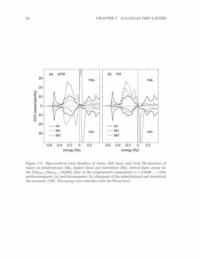
82 CHAPTER 7. (GA,MN)AS THIN LAYERS
30
20
10
0
10
20
30
-0.6 -0.4 -0.2 0 0.2
DO
S (
stat
es/s
pin/
Ry)
energy (Ry)
maj.
min.
totMn
Mni
(a) AFM
-0.6 -0.4 -0.2 0 0.2
energy (Ry)
maj.
min.
totMn
Mni
(b) FM
Figure 7.5: Spin-resolved total densities of states (full lines) and local Mn-densities ofstates on substitutional (Mn, dashed lines) and interstitial (Mni, dotted lines) atoms forthe (Ga0.95+zMn0.05−z)AsMni
z alloy at the compensated composition (z = 0.0166 . . . ) withantiferromagnetic (a) and ferromagnetic (b) alignment of the substitutional and interstitialMn-moments [130]. The energy zero coincides with the Fermi level.
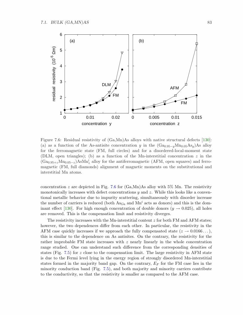
7.1. BULK (GA,MN)AS 83
1
2
3
4
5
6
0 0.01 0.02
resi
dual
res
istiv
ity (
10-5
Ωm
)
concentration y
(a)
DLM
FM
0 0.005 0.01 0.015
concentration z
(b)
AFM
FM
Figure 7.6: Residual resistivity of (Ga,Mn)As alloys with native structural defects [130]:(a) as a function of the As-antisite concentration y in the (Ga0.95−yMn0.05Asy)As alloyfor the ferromagnetic state (FM, full circles) and for a disordered-local-moment state(DLM, open triangles); (b) as a function of the Mn-interstitial concentration z in the(Ga0.95+zMn0.05−z)AsMni
z alloy for the antiferromagnetic (AFM, open squares) and ferro-magnetic (FM, full diamonds) alignment of magnetic moments on the substitutional andinterstitial Mn atoms.
concentration z are depicted in Fig. 7.6 for (Ga,Mn)As alloy with 5% Mn. The resistivitymonotonically increases with defect concentrations y and z. While this looks like a conven-tional metallic behavior due to impurity scattering, simultaneously with disorder increasethe number of carriers is reduced (both AsGa and Mni acts as donors) and this is the dom-inant effect [130]. For high enough concentration of double donors (y → 0.025), all holesare removed. This is the compensation limit and resistivity diverges.
The resistivity increases with the Mn-interstitial content z for both FM and AFM states;however, the two dependences differ from each other. In particular, the resistivity in theAFM case quickly increases if we approach the fully compensated state (z → 0.0166 . . . ),this is similar to the dependence on As antisites. On the contrary, the resistivity for therather improbable FM state increases with z nearly linearly in the whole concentrationrange studied. One can understand such difference from the corresponding densities ofstates (Fig. 7.5) for z close to the compensation limit. The large resistivity in AFM stateis due to the Fermi level lying in the energy region of strongly disordered Mn-interstitialstates formed in the majority band gap. On the contrary, EF for the FM case lies in theminority conduction band (Fig. 7.5), and both majority and minority carriers contributeto the conductivity, so that the resistivity is smaller as compared to the AFM case.
84 CHAPTER 7. (GA,MN)AS THIN LAYERS
7.1.2 Uncompensated DLM state
Recent theoretical studies indicate that magnetic structures with partial disorder of lo-cal magnetic moments (pDLM) can lower the total energy of system with lattice defects ascompared to the ferromagnetic state [134]. This structure can be described as an alloy com-prising two oppositely oriented Mn atoms: (Ga1−x−yMn+
(1+r)x/2Mn−(1−r)x/2Asy)As, wherer is an auxiliary order parameter (0 ≤ r ≤ 1) which specifies the fraction of Mn atomswith local moments oriented oppositely to the remaining Mn-moments. The concentrationsof Mn+ and Mn− atoms are x+ and x− respectively. The order parameter is defined asr = (x+ − x−) /x, therefore x± = (1± r)x/2. Magnetic moments are not completely dis-ordered unless r = 0, the system retains a nonzero average magnetic moment lower thanthat of its FM phase, this case is also called uncompensated DLM state.
In ref. [134] it is shown that for a situation without As antisites the oppositely orientedMn− moments would form a very narrow impurity band located exactly at the Fermilevel, which is energetically very unfavorable situation and forces Mn moments to the FMstate. However the enough amount of extra electrons donated by As antisites cause theimpurity subband of Mn− to lay completely below the Fermi level thus being energeticallyinexpensive. The shift of EF therefore contributes to energetic stabilization of the DLMstate as well as to the full spin polarization of the DLM conductivities. Ab initio calculationscan evaluate the energy associated with each amount of magnetic disorder (parameter r),depicted in Fig. 7.7. Thus they reveal the threshold value of As antisites concentrationy leading to partial DLM (Fig. 7.8 for various Mn-content x) and determine the orderparameter associated with each y.
The presence of additional disorder of course increases the amount of scattering, itsinfluence on the residual resistivity can be seen in Fig. 7.6. Calculations of conductanceshows that the transport remains completely spin polarized up to quite high values ofantisite disorder, in agreement with the finding that Mn− states (potentially destroying thefull spin polarization) are located mainly below the Fermi level. Their contribution to spinpolarization is negligible up to y ≤ 0.02 (and x = 0.05), for higher values the correspondingstrong magnetic disorder (r > 0.3) starts to influence the DOS heavily [135].
7.2 Ideal (Ga,Mn)As layers coupled to metallic leads
The interesting influence of (Ga,Mn)As on conductance spin polarization can be utilizedin systems where it is comprised in a form of layers with nanoscale thickness. A tunnelingjunction comprising two such layers has already been prepared [136], yielding an impressiveTMR of 290% at 0.39K. Here we examine properties of its basic elements, single thin(Ga,Mn)As slabs, which may provide important information for construction of arbitraryspintronics devices based on it.
The calculations reported here were performed for (001) layers of zinc-blende Ga1−xMnxAsalloys with Mn content in a range 0.03 ≤ x ≤ 0.10, sandwiched by two semi-infinite bcc(001)leads of nonmagnetic chromium. The lattice (Ga,Mn)As is equivalent to four inpenetratingfcc lattices as described in sec. 7.1. These two different lattices allow quite precise match-ing, where the lattice constant abcc =
√2afcc. One atomic (001) layer of the resulting bcc
lattice thus contained two spheres: either a Ga sphere and an empty sphere or an As sphere
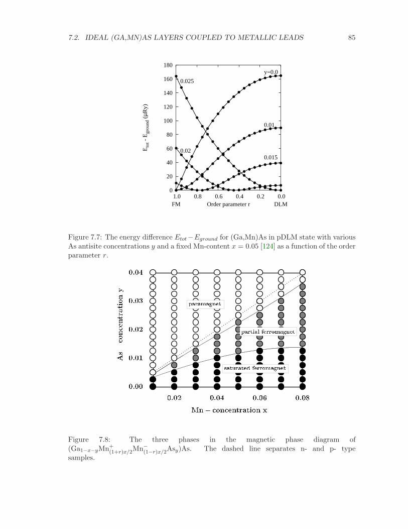
7.2. IDEAL (GA,MN)AS LAYERS COUPLED TO METALLIC LEADS 85
0
20
40
60
80
100
120
140
160
180
1.0 0.8 0.6 0.4 0.2 0.0
Eto
t - E
grou
nd (
µRy)
Order parameter r
0.025
0.020.015
0.01
y=0.0
FM DLM
Fig. 1b
Figure 7.7: The energy difference Etot−Eground for (Ga,Mn)As in pDLM state with variousAs antisite concentrations y and a fixed Mn-content x = 0.05 [124] as a function of the orderparameter r.
0.000.010.020.030.04
0.02 0.04 0.06 0.08Mn on entration xAs on entrationy paramagnet partial ferromagnet
saturated ferromagnetFigure 7.8: The three phases in the magnetic phase diagram of(Ga1−x−yMn+
(1+r)x/2Mn−(1−r)x/2Asy)As. The dashed line separates n- and p- typesamples.
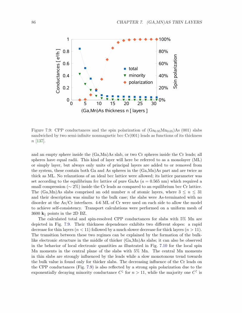
86 CHAPTER 7. (GA,MN)AS THIN LAYERS
Figure 7.9: CPP conductances and the spin polarization of (Ga0.95Mn0.05)As (001) slabssandwiched by two semi-infinite nonmagnetic bcc Cr(001) leads as functions of its thicknessn [137].
and an empty sphere inside the (Ga,Mn)As slab, or two Cr spheres inside the Cr leads; allspheres have equal radii. This kind of layer will here be referred to as a monolayer (ML)or simply layer, but always only units of principal layers are added to or removed fromthe system, these contain both Ga and As spheres in the (Ga,Mn)As part and are twice asthick as ML. No relaxations of an ideal bcc lattice were allowed; its lattice parameter wasset according to the equilibrium fcc lattice of pure GaAs (a = 0.565 nm) which required asmall compression (∼ 2%) inside the Cr leads as compared to an equilibrium bcc Cr lattice.The (Ga,Mn)As slabs comprised an odd number n of atomic layers, where 3 ≤ n ≤ 31and their description was similar to the bulk case; the slabs were As-terminated with nodisorder at the As/Cr interfaces. 4-6 ML of Cr were used on each side to allow the modelto achieve self-consistency. Transport calculations were performed on a uniform mesh of3600 k‖ points in the 2D BZ.
The calculated total and spin-resolved CPP conductances for slabs with 5% Mn aredepicted in Fig. 7.9. Their thickness dependence exhibits two different slopes: a rapiddecrease for thin layers (n < 11) followed by a much slower decrease for thick layers (n > 11).The transition between these two regimes can be explained by the formation of the bulk-like electronic structure in the middle of thicker (Ga,Mn)As slabs; it can also be observedin the behavior of local electronic quantities as illustrated in Fig. 7.10 for the local spinMn moments in the central plane of the slabs with 5% Mn. The central Mn momentsin thin slabs are strongly influenced by the leads while a slow monotonous trend towardsthe bulk value is found only for thicker slabs. The decreasing influence of the Cr leads onthe CPP conductances (Fig. 7.9) is also reflected by a strong spin polarization due to theexponentially decaying minority conductance C↓ for n > 11, while the majority one C↑ is
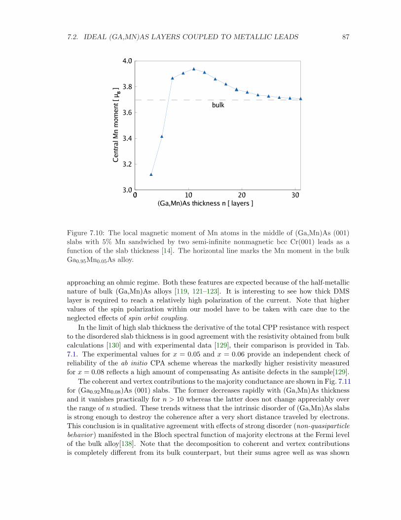
7.2. IDEAL (GA,MN)AS LAYERS COUPLED TO METALLIC LEADS 87
Figure 7.10: The local magnetic moment of Mn atoms in the middle of (Ga,Mn)As (001)slabs with 5% Mn sandwiched by two semi-infinite nonmagnetic bcc Cr(001) leads as afunction of the slab thickness [14]. The horizontal line marks the Mn moment in the bulkGa0.95Mn0.05As alloy.
approaching an ohmic regime. Both these features are expected because of the half-metallicnature of bulk (Ga,Mn)As alloys [119, 121–123]. It is interesting to see how thick DMSlayer is required to reach a relatively high polarization of the current. Note that highervalues of the spin polarization within our model have to be taken with care due to theneglected effects of spin orbit coupling.
In the limit of high slab thickness the derivative of the total CPP resistance with respectto the disordered slab thickness is in good agreement with the resistivity obtained from bulkcalculations [130] and with experimental data [129], their comparison is provided in Tab.7.1. The experimental values for x = 0.05 and x = 0.06 provide an independent check ofreliability of the ab initio CPA scheme whereas the markedly higher resistivity measuredfor x = 0.08 reflects a high amount of compensating As antisite defects in the sample[129].
The coherent and vertex contributions to the majority conductance are shown in Fig. 7.11for (Ga0.92Mn0.08)As (001) slabs. The former decreases rapidly with (Ga,Mn)As thicknessand it vanishes practically for n > 10 whereas the latter does not change appreciably overthe range of n studied. These trends witness that the intrinsic disorder of (Ga,Mn)As slabsis strong enough to destroy the coherence after a very short distance traveled by electrons.This conclusion is in qualitative agreement with effects of strong disorder (non-quasiparticlebehavior) manifested in the Bloch spectral function of majority electrons at the Fermi levelof the bulk alloy[138]. Note that the decomposition to coherent and vertex contributionsis completely different from its bulk counterpart, but their sums agree well as was shown
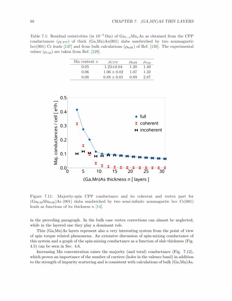
88 CHAPTER 7. (GA,MN)AS THIN LAYERS
Table 7.1: Residual resistivities (in 10−5 Ωm) of Ga1−xMnxAs as obtained from the CPPconductances (ρCPP ) of thick (Ga,Mn)As(001) slabs sandwiched by two nonmagneticbcc(001) Cr leads [137] and from bulk calculations (ρbulk) of Ref. [130]. The experimentalvalues (ρexp) are taken from Ref. [129].
Mn content x ρCPP ρbulk ρexp
0.05 1.23±0.04 1.20 1.490.06 1.06± 0.02 1.07 1.320.08 0.88± 0.01 0.89 2.87
Figure 7.11: Majority-spin CPP conductance and its coherent and vertex part for(Ga0.92Mn0.08)As (001) slabs sandwiched by two semi-infinite nonmagnetic bcc Cr(001)leads as functions of its thickness n [14].
in the preceding paragraph. In the bulk case vertex corrections can almost be neglected,while in the layered one they play a dominant role.
Thin (Ga,Mn)As layers represent also a very interesting system from the point of viewof spin torque related phenomena. An extensive discussion of spin-mixing conductance ofthis system and a graph of the spin-mixing conductance as a function of slab thickness (Fig.4.5) can be seen in Sec. 4.6.
Increasing Mn concentration raises the majority (and total) conductance (Fig. 7.12),which proves an importance of the number of carriers (holes in the valence band) in additionto the strength of impurity scattering and is consistent with calculations of bulk (Ga,Mn)As.
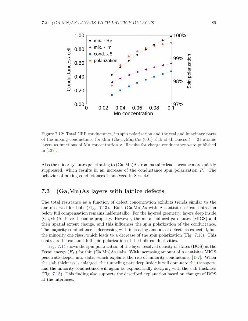
7.3. (GA,MN)AS LAYERS WITH LATTICE DEFECTS 89
Figure 7.12: Total CPP conductance, its spin polarization and the real and imaginary partsof the mixing conductance for thin (Ga1−xMnx)As (001) slab of thickness t = 21 atomiclayers as functions of Mn concentration x. Results for charge conductance were publishedin [137].
Also the minority states penetrating to (Ga,Mn)As from metallic leads become more quicklysuppressed, which results in an increase of the conductance spin polarization P . Thebehavior of mixing conductances is analyzed in Sec. 4.6.
7.3 (Ga,Mn)As layers with lattice defects
The total resistance as a function of defect concentration exhibits trends similar to theone observed for bulk (Fig. 7.13). Bulk (Ga,Mn)As with As antisites of concentrationbelow full compensation remains half-metallic. For the layered geometry, layers deep inside(Ga,Mn)As have the same property. However, the metal induced gap states (MIGS) andtheir spatial extent change, and this influences the spin polarization of the conductance.The majority conductance is decreasing with increasing amount of defects as expected, butthe minority one rises, which leads to a decrease of the spin polarization (Fig. 7.13). Thiscontrasts the constant full spin polarization of the bulk conductivities.
Fig. 7.14 shows the spin polarization of the layer-resolved density of states (DOS) at theFermi energy (EF ) for thin (Ga,Mn)As slabs. With increasing amount of As antisites MIGSpenetrate deeper into slabs, which explains the rise of minority conductance [137]. Whenthe slab thickness is enlarged, the tunneling part deep inside it will dominate the transport,and the minority conductance will again be exponentially decaying with the slab thickness(Fig. 7.15). This finding also supports the described explanation based on changes of DOSat the interfaces.
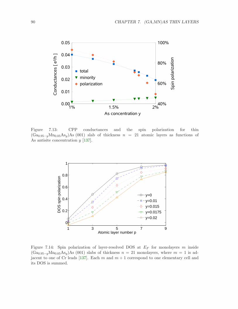
90 CHAPTER 7. (GA,MN)AS THIN LAYERS
Figure 7.13: CPP conductances and the spin polarization for thin(Ga0.95−yMn0.05Asy)As (001) slab of thickness n = 21 atomic layers as functions ofAs antisite concentration y [137].
1 3 5 7 9
0
0.2
0.4
0.6
0.8
1
Atomic layer number p
DO
S s
pin
pola
rizat
ion
y=0
y=0.01
y=0.015
y=0.0175
y=0.02
Figure 7.14: Spin polarization of layer-resolved DOS at EF for monolayers m inside(Ga0.95−yMn0.05Asy)As (001) slabs of thickness n = 21 monolayers, where m = 1 is ad-jacent to one of Cr leads [137]. Each m and m + 1 correspond to one elementary cell andits DOS is summed.
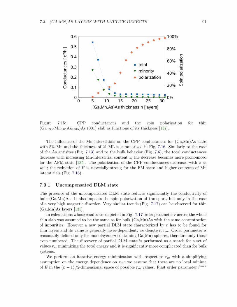
7.3. (GA,MN)AS LAYERS WITH LATTICE DEFECTS 91
Figure 7.15: CPP conductances and the spin polarization for thin(Ga0.935Mn0.05As0.015)As (001) slab as functions of its thickness [137].
The influence of the Mn interstitials on the CPP conductances for (Ga,Mn)As slabswith 5% Mn and the thickness of 21 ML is summarized in Fig. 7.16. Similarly to the caseof the As antisites (Fig. 7.13) and to the bulk behavior (Fig. 7.6), the total conductancesdecrease with increasing Mn-interstitial content z; the decrease becomes more pronouncedfor the AFM state [135]. The polarization of the CPP conductances decreases with z aswell; the reduction of P is especially strong for the FM state and higher contents of Mninterstitials (Fig. 7.16).
7.3.1 Uncompensated DLM state
The presence of the uncompensated DLM state reduces significantly the conductivity ofbulk (Ga,Mn)As. It also impacts the spin polarization of transport, but only in the caseof a very high magnetic disorder. Very similar trends (Fig. 7.17) can be observed for thin(Ga,Mn)As layers [135].
In calculations whose results are depicted in Fig. 7.17 order parameter r across the wholethin slab was assumed to be the same as for bulk (Ga,Mn)As with the same concentrationof impurities. However a new partial DLM state characterized by r has to be found forthin layers and its value is generally layer-dependent, we denote it rm. Order parameter isreasonably defined only for monolayers m containing Ga(Mn) spheres, therefore only thoseeven numbered. The discovery of partial DLM state is performed as a search for a set ofvalues rm minimizing the total energy and it is significantly more complicated than for bulksystems.
We perform an iterative energy minimization with respect to rm with a simplifyingassumption on the energy dependence on rm: we assume that there are no local minimaof E in the (n− 1) /2-dimensional space of possible rm values. First order parameter rmin
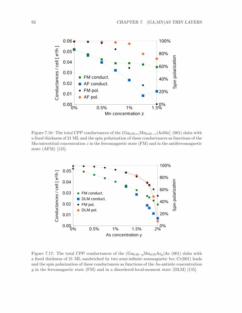
92 CHAPTER 7. (GA,MN)AS THIN LAYERS
Figure 7.16: The total CPP conductances of the (Ga0.95+zMn0.05−z)AsMniz (001) slabs with
a fixed thickness of 21 ML and the spin polarization of these conductances as functions of theMn-interstitial concentration z in the ferromagnetic state (FM) and in the antiferromagneticstate (AFM) [135].
Figure 7.17: The total CPP conductances of the (Ga0.95−yMn0.05Asy)As (001) slabs witha fixed thickness of 21 ML sandwiched by two semi-infinite nonmagnetic bcc Cr(001) leadsand the spin polarization of these conductances as functions of the As-antisite concentrationy in the ferromagnetic state (FM) and in a disordered-local-moment state (DLM) [135].
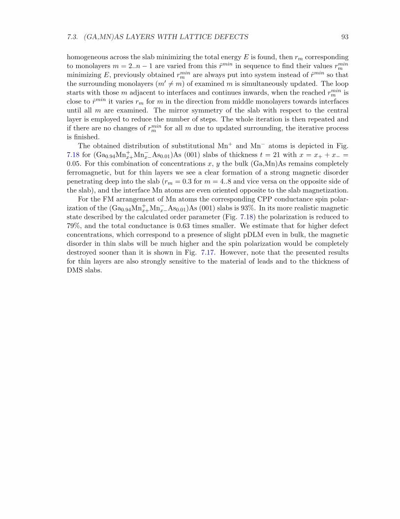
7.3. (GA,MN)AS LAYERS WITH LATTICE DEFECTS 93
homogeneous across the slab minimizing the total energy E is found, then rm correspondingto monolayers m = 2..n− 1 are varied from this rmin in sequence to find their values rmin
m
minimizing E, previously obtained rminm are always put into system instead of rmin so that
the surrounding monolayers (m′ 6= m) of examined m is simultaneously updated. The loopstarts with those m adjacent to interfaces and continues inwards, when the reached rmin
m isclose to rmin it varies rm for m in the direction from middle monolayers towards interfacesuntil all m are examined. The mirror symmetry of the slab with respect to the centrallayer is employed to reduce the number of steps. The whole iteration is then repeated andif there are no changes of rmin
m for all m due to updated surrounding, the iterative processis finished.
The obtained distribution of substitutional Mn+ and Mn− atoms is depicted in Fig.7.18 for (Ga0.94Mn+
x+Mn−x−As0.01)As (001) slabs of thickness t = 21 with x = x+ + x− =0.05. For this combination of concentrations x, y the bulk (Ga,Mn)As remains completelyferromagnetic, but for thin layers we see a clear formation of a strong magnetic disorderpenetrating deep into the slab (rm = 0.3 for m = 4..8 and vice versa on the opposite side ofthe slab), and the interface Mn atoms are even oriented opposite to the slab magnetization.
For the FM arrangement of Mn atoms the corresponding CPP conductance spin polar-ization of the (Ga0.94Mn+
x+Mn−x−As0.01)As (001) slabs is 93%. In its more realistic magneticstate described by the calculated order parameter (Fig. 7.18) the polarization is reduced to79%, and the total conductance is 0.63 times smaller. We estimate that for higher defectconcentrations, which correspond to a presence of slight pDLM even in bulk, the magneticdisorder in thin slabs will be much higher and the spin polarization would be completelydestroyed sooner than it is shown in Fig. 7.17. However, note that the presented resultsfor thin layers are also strongly sensitive to the material of leads and to the thickness ofDMS slabs.
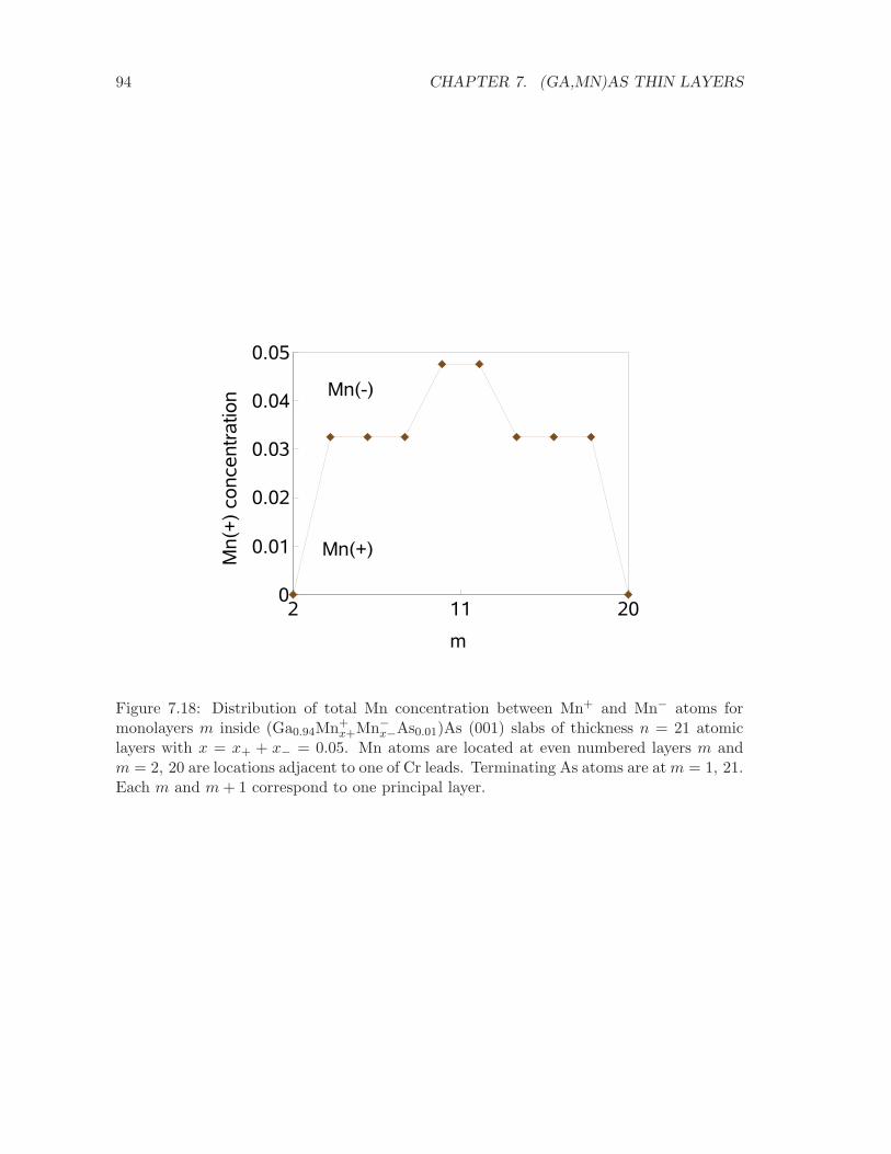
94 CHAPTER 7. (GA,MN)AS THIN LAYERS
Figure 7.18: Distribution of total Mn concentration between Mn+ and Mn− atoms formonolayers m inside (Ga0.94Mn+
x+Mn−x−As0.01)As (001) slabs of thickness n = 21 atomiclayers with x = x+ + x− = 0.05. Mn atoms are located at even numbered layers m andm = 2, 20 are locations adjacent to one of Cr leads. Terminating As atoms are atm = 1, 21.Each m and m+ 1 correspond to one principal layer.
Chapter 8
Co2MnSi thin layers
The intermetallic compound Co2MnSi is chosen here as a representative of the wide class offull Heusler alloys. This name originates from Friedrich Heusler’s discovery of ferromagneticalloy Cu2MnAl, whose all elements are non-magnetic. Later the name was adopted for allintermetallic compounds with similar structure and the first discovered half-metal belongsto this class [24]. It can be viewed as 4 inpenetrating fcc lattices (Fig. 8.1) with latticeparameter (a = 0.565 nm) very close to that of GaAs, which allows very good matching toit.
Halfmetallicity is common among Heusler alloys, and Co2MnSi also should have thisproperty according to ab initio calculations [139]. However, attempts to prove this exper-imentally were not successful until recently, when the halfmetallic energy gap in Co2MnSiwas observed by tunneling conductance spectroscopy [140, 141]. There are few most prob-able reasons for difficulties with confirming halfmetallicity of this structure [142]:
• The used methods are often surface sensitive, but the half-metallic character is de-stroyed at surfaces.
• Antisite disorder is likely to occur, especially swapping between Mn atoms and similarsized Co atoms, which are also close to each other
One of the most important advantages of Co2MnSi over other halfmetals is its high Curietemperature 985K, magnon effects can be neglected even at room temperature [143]. An-other crucial feature is the expected width of the minority bandgap, which should preservethe half-metalicity even at room temperature (depending on the position of the Fermienergy inside the gap). Therefore this material is definitely worth further examination.
8.1 Bulk properties
The calculated band structure and density of states of ideal Co2MnSi are depicted in Fig. 8.2and the left panel of Fig. 8.3, respectively. Transport calculations show zero conductancein the minority spin channel as expected because of its predicted half-metallic character.Calculated magnetic moment is 5 µB per f. u. (formula unit), in agreement with thefact that conduction band is cut by Fermi level for one spin channel only, hence there
95
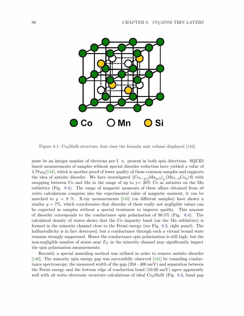
96 CHAPTER 8. CO2MNSI THIN LAYERS
Figure 8.1: Co2MnSi structure, four time the formula unit volume displayed [142].
must be an integer number of electrons per f. u. present in both spin directions. SQUIDbased measurements of samples without special disorder reduction have yielded a value of4.78µB[144], which is another proof of lower quality of these common samples and supportsthe idea of antisite disorder. We have investigated
(Co1−y/2Mny/2
)2(Mn1−yCoy) Si with
swapping between Co and Mn in the range of up to y= 20% Co as antisites on the Mnsublattice (Fig. 8.4). The range of magnetic moments of these alloys obtained from abinitio calculations comprise also the experimental value of magnetic moment, it can bematched to y = 8 %. X-ray measurements [145] (on different samples) have shown asimilar y = 7%, which corroborates that disorder of these really not negligible values canbe expected in samples without a special treatment to improve quality. This amountof disorder corresponds to the conductance spin polarization of 98.5% (Fig. 8.4). Thecalculated density of states shows that the Co impurity band (on the Mn sublattice) isformed in the minority channel close to the Fermi energy (see Fig. 8.3, right panel). Thehalfmetallicity is in fact destroyed, but a conductance through such a virtual bound stateremains strongly suppressed. Hence the conductance spin polarization is still high, but thenon-negligible number of states near EF in the minority channel may significantly impactthe spin polarization measurements.
Recently a special annealing method was utilized in order to remove antisite disorder[140]. The minority spin energy gap was successfully observed [141] by tunneling conduc-tance spectroscopy, the measured width of the gap (350 - 400 meV) and separation betweenthe Fermi energy and the bottom edge of conduction band (10-20 meV) agree apparentlywell with ab initio electronic structure calculations of ideal Co2MnSi (Fig. 8.3, band gap
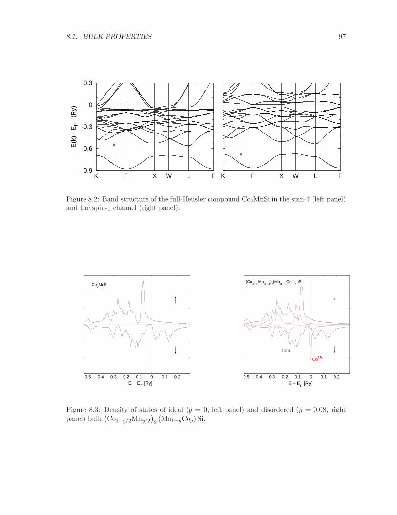
8.1. BULK PROPERTIES 97
-0.9
-0.6
-0.3
0
0.3
E(k
) -
EF
(Ry)
K Γ X W L Γ K Γ X W L Γ
Figure 8.2: Band structure of the full-Heusler compound Co2MnSi in the spin-↑ (left panel)and the spin-↓ channel (right panel).
−0.5 −0.4 −0.3 −0.2 −0.1 0 0.1 0.2−150
−100
−50
0
50
100
150
E − EF [Ry]
Co2MnSi
−0.5 −0.4 −0.3 −0.2 −0.1 0 0.1 0.2−150
−100
−50
0
50
100
150
E − EF [Ry]
total
CoMn
(Co0.96
Mn0.04
)2(Mn
0.92Co
0.08)Si
Figure 8.3: Density of states of ideal (y = 0, left panel) and disordered (y = 0.08, rightpanel) bulk
(Co1−y/2Mny/2
)2(Mn1−yCoy) Si.
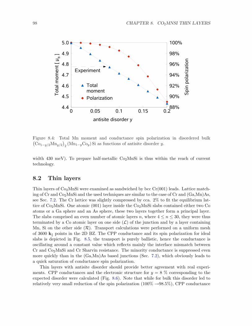
98 CHAPTER 8. CO2MNSI THIN LAYERS
Figure 8.4: Total Mn moment and conductance spin polarization in disordered bulk(Co1−y/2Mny/2
)2(Mn1−yCoy) Si as functions of antisite disorder y.
width 430 meV). To prepare half-metallic Co2MnSi is thus within the reach of currenttechnology.
8.2 Thin layers
Thin layers of Co2MnSi were examined as sandwiched by bcc Cr(001) leads. Lattice match-ing of Cr and Co2MnSi and the used techniques are similar to the case of Cr and (Ga,Mn)As,see Sec. 7.2. The Cr lattice was slightly compressed by cca. 2% to fit the equilibrium lat-tice of Co2MnSi. One atomic (001) layer inside the Co2MnSi slabs contained either two Coatoms or a Ga sphere and an As sphere, these two layers together form a principal layer.The slabs comprised an even number of atomic layers n, where 4 ≤ n ≤ 30, they were thusterminated by a Co atomic layer on one side (L) of the junction and by a layer containingMn, Si on the other side (R). Transport calculations were performed on a uniform meshof 3600 k‖ points in the 2D BZ. The CPP conductance and its spin polarization for idealslabs is depicted in Fig. 8.5, the transport is purely ballistic, hence the conductance isoscillating around a constant value which reflects mainly the interface mismatch betweenCr and Co2MnSi and Cr Sharvin resistance. The minority conductance is suppressed evenmore quickly than in the (Ga,Mn)As based junctions (Sec. 7.2), which obviously leads toa quick saturation of conductance spin polarization.
Thin layers with antisite disorder should provide better agreement with real experi-ments. CPP conductances and the electronic structure for y = 8 % corresponding to theexpected disorder were calculated (Fig. 8.6). Note that while for bulk this disorder led torelatively very small reduction of the spin polarization (100% →98.5%), CPP conductance
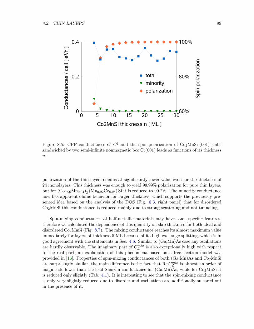
8.2. THIN LAYERS 99
Figure 8.5: CPP conductances C, C↓ and the spin polarization of Co2MnSi (001) slabssandwiched by two semi-infinite nonmagnetic bcc Cr(001) leads as functions of its thicknessn.
polarization of the thin layer remains at significantly lower value even for the thickness of24 monolayers. This thickness was enough to yield 99.99% polarization for pure thin layers,but for (Co0.96Mn0.04)2 (Mn0.92Co0.08) Si it is reduced to 90.2%. The minority conductancenow has apparent ohmic behavior for larger thickness, which supports the previously pre-sented idea based on the analysis of the DOS (Fig. 8.3, right panel) that for disorderedCo2MnSi this conductance is reduced mainly due to strong scattering and not tunneling.
Spin-mixing conductances of half-metallic materials may have some specific features,therefore we calculated the dependence of this quantity on slab thickness for both ideal anddisordered Co2MnSi (Fig. 8.7). The mixing conductance reaches its almost maximum valueimmediately for layers of thickness 5 ML because of its high exchange splitting, which is ingood agreement with the statements in Sec. 4.6. Similar to (Ga,Mn)As case any oscillationsare hardly observable. The imaginary part of Cmix
L is also exceptionally high with respectto the real part, an explanation of this phenomena based on a free-electron model wasprovided in [16]. Properties of spin-mixing conductances of both (Ga,Mn)As and Co2MnSiare surprisingly similar, the main difference is the fact that ReCmix
L is almost an order ofmagnitude lower than the lead Sharvin conductance for (Ga,Mn)As, while for Co2MnSi itis reduced only slightly (Tab. 4.1). It is interesting to see that the spin-mixing conductanceis only very slightly reduced due to disorder and oscillations are additionally smeared outin the presence of it.
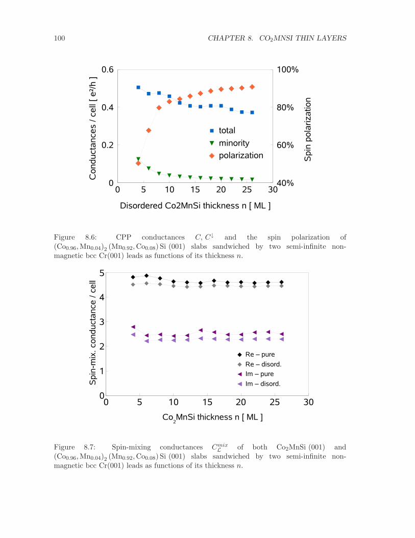
100 CHAPTER 8. CO2MNSI THIN LAYERS
Figure 8.6: CPP conductances C, C↓ and the spin polarization of(Co0.96,Mn0.04)2 (Mn0.92,Co0.08) Si (001) slabs sandwiched by two semi-infinite non-magnetic bcc Cr(001) leads as functions of its thickness n.
Figure 8.7: Spin-mixing conductances CmixL of both Co2MnSi (001) and
(Co0.96,Mn0.04)2 (Mn0.92,Co0.08) Si (001) slabs sandwiched by two semi-infinite non-magnetic bcc Cr(001) leads as functions of its thickness n.
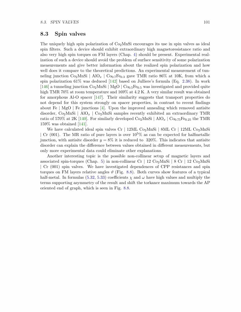
8.3. SPIN VALVES 101
8.3 Spin valves
The uniquely high spin polarization of Co2MnSi encourages its use in spin valves as idealspin filters. Such a device should exhibit extraordinary high magnetoresistance ratio andalso very high spin torques on FM layers (Chap. 4) should be present. Experimental real-ization of such a device should avoid the problem of surface sensitivity of some polarizationmeasurements and give better information about the realized spin polarization and howwell does it compare to the theoretical predictions. An experimental measurement of tun-neling junction Co2MnSi | AlOx | Co0.7Fe0.3 gave TMR ratio 86% at 10K, from which aspin polarization 61% was deduced [142] based on Julliere’s formula (Eq. 2.38). In work[146] a tunneling junction Co2MnSi | MgO | Co0.5Fe0.5 was investigated and provided quitehigh TMR 70% at room temperature and 169% at 4.2 K. A very similar result was obtainedfor amorphous Al-O spacer [147]. Their similarity suggests that transport properties donot depend for this system strongly on spacer properties, in contrast to recent findingsabout Fe | MgO | Fe junctions [4]. Upon the improved annealing which removed antisitedisorder, Co2MnSi | AlOx | Co2MnSi samples recently exhibited an extraordinary TMRratio of 570% at 2K [140]. For similarly developed Co2MnSi | AlOx | Co0.75Fe0.25 the TMR159% was obtained [141].
We have calculated ideal spin valves Cr | 12ML Co2MnSi | 8ML Cr | 12ML Co2MnSi| Cr (001). The MR ratio of pure layers is over 105% as can be expected for halfmetallicjunction, with antisite disorder y = 8% it is reduced to 320%. This indicates that antisitedisorder can explain the difference between values obtained in different measurements, butonly more experimental data could eliminate other explanations.
Another interesting topic is the possible non-collinear setup of magnetic layers andassociated spin-torques (Chap. 5) in non-collinear Cr | 12 Co2MnSi | 8 Cr | 12 Co2MnSi| Cr (001) spin valves. We have investigated dependences of CPP resistances and spintorques on FM layers relative angles ϑ (Fig. 8.8). Both curves show features of a typicalhalf-metal. In formulas (5.32, 5.33) coefficients χ and ω have high values and multiply theterms supporting asymmetry of the result and shift the torkance maximum towards the APoriented end of graph, which is seen in Fig. 8.8.
102 CHAPTER 8. CO2MNSI THIN LAYERS
Figure 8.8: CPP resistances and the spin torque exerted on the second FM layer of the Cr| 12ML Co2MnSi | 8ML Cr | 12ML Co2MnSi | Cr bilayer as functions of FM layers relativeangle ϑ from ab initio calculations (markers) compared to empirical formula results (lines)
Chapter 9
Conclusions
The theoretical part of this work was aimed mainly towards a development of very generalab initio methods. First we have enlarged the range of materials that can be handled byexisting approaches: transport properties calculations for disordered systems based on theCPA were extended from bulk materials also to systems with one reduced dimension, mul-tilayers. We have shown the importance of vertex corrections for this particular situation.This kind of problems can be evaluated on ab initio level also by means of the supercellmethod, but for some materials or situations our method appears to be more suitable, forexample for the diluted magnetic semiconductors. Comparison of the supercell and the fullCPA results proves that important aspects of the spin-polarized CPP transport are fullywithin the reach of an effective medium treatment (Sec. 6.2.2, 6.3).
Secondly we have derived ab initio methods for evaluation of novel observables connectedwith the phenomena of current induced magnetization switching, namely the spin-mixingconductance and spin torque. This area is yet only scarcely examined and we believe thatour work has contributed significantly to understanding of this phenomenon, we have forexample revealed its connection to system Green’s functions (Eqs. 4.19, 4.20, 4.21). Forthe first time the spin-mixing conductance was combined with the CPA approximation fordisordered systems. We have also demonstrated the equivalence between the Kubo andNEGF approach within linear response regime for one particular direction of spin-mixingconductance. The key features of our technique are the correct inclusion of evanescentstates and the fact that it can be treated in a similar way as the charge conductance, thusit is compatible with the previously mentioned method for disordered systems. This generalformulation of mixing conductances allows to find whether some often adopted assumptionsare correct in all situations. Namely the assumption of a fast convergence of spin-mixingconductance with increasing thickness is found not to be valid for thin Ni layers (Fig. 4.3).Imaginary part of the mixing conductance was believed to be much smaller than the realpart, this was disproven here for thin layers of (Ga,Mn)As (Fig. 4.5) or Co2MnSi (Tab.4.1, Fig. 8.7). A compact Caroli-like formula was formulated for spin torque caused byCPP current in non-collinear magnetic layered systems (Eq. 5.23). The relation betweenspin-mixing conductances and spin torques in non-collinear magnetic junctions has beenfound to be quite close (Sec. 5.3) and the theory has been shown to be capable of dealingwith arbitrary angular arrangements of magnetic layers (Sec. 5.4.1). In the future thisapproach to non-collinear systems can be combined with the CPA too and the spin-orbit
103
104 CHAPTER 9. CONCLUSIONS
coupling may also be included with no major obstacles.The second part containing informations about concrete materials served two purposes.
First it was used to test the presented methods. The systems were therefore selected so thatthey were as diverse as possible. Its results were compared to experimental data or othercomputational results if available, and the agreement was generally within the expectedaccuracy. Predictions for observable and material combination without relevant previousinformation were tested successfully for symmetries and conditions it should fulfill and atleast the trends were found appropriate to what can be expected according to materialproperties. Therefore the developed methods appear to have passed the tests, and thechosen approximations were appropriate. The second main purpose was to find more infor-mation about the selected systems, explain not yet understood phenomena and predict itsbehavior under yet untested conditions, therefore we attempted to choose primarily physi-cally interesting systems with unique or novel features or systems with a high applicationpotential.
For thin (Ga,Mn)As layers many presented findings are novel since almost all existingab initio studies deal only with its bulk counterpart. The obtained transport properties hastherefore been checked for compatibility with calculated and measured bulk data, whichturned out to be successful (Tab. 7.1). Very interesting is the discovered relation betweenthe current spin polarization and native structural defects (Sec. 7.3). We have providedan explanation of this dependence based on the variation of metal induced gap states. Wewere also the first to calculate the spin-mixing conductance of this system and some resultsare rather surprising, especially the already mentioned magnitude of its imaginary part.Although we do not believe that the Curie temperature of (Ga,Mn)As can be raised highenough to allow practical utilization of this material, the same ideas can be more or lessapplied to other diluted magnetic semiconductors. In this class of materials there are someother promising novel types which may overcome the Curie temperature problem, in thiscontext Li(Zn,Mn)As has been proposed recently [148].
Interest in Heusler alloys is high because of its unique features. An obstacle for obtain-ing theoretically predicted features in Co2MnSi is its high tendency to antisite disorder,which leads quickly to a loss of halfmetallicity, we have calculated its impact on transportproperties of thin Co2MnSi layers (Sec. 8.2). Its direct elimination did not appear to beeasily doable, but very recent experiments seems to have overcome this problem[140]. Ourresults may help to understand how the expected total spin polarization can be reached.We examined the angular dependence of spin torque (Fig. 8.8) exerted on one part of aspin valve constructed from such almost ideal spin-filter, this may be very important forattempts to create CIMS based applications of this or a similar material.
Appendix A
Derivation of Kubo formula forgeneralized CPP transport
The starting formula (2.47) can be rewritten using Eq. (2.5):
CAB =i
2πlim
α→0+
∫dξf (ξ) Tr
[G (ξ + i0)−G (ξ − i0)]AG (ξ + iα) B (A.1)
+G (ξ − iα)A [G (ξ + i0)−G (ξ − i0)] B.
We decompose the last equation to three contributions distinguished by the sign of theimaginary parts of both complex energy arguments, labeled as:
• CP ... for both imaginary parts positive
• CN ... for both imaginary parts negative
• CM ... for imaginary parts with mixed signs
The following commutator allows to revert the order of G (z) and B:[G (z) , B
]= G (z)
(B (z −H)− (z −H) B
)G (z) = −iG (z) AG (z) .
From this a relation corresponding to our problem can be derived:
TrAG (zµ) BG (zν)
= Tr
ABG (zµ)G (zν)
− iTr
AG (zµ) AG (zµ)G (zν)
, (A.2)
or alternatively
TrAG (zµ) BG (zν)
= Tr
AG (zµ)G (zν) B
+ iTr
AG (zµ)G (zν) AG (zµ)
. (A.3)
We employ (A.2) for the part of (A.1) corresponding to CM :
CM1 =
i
2πlim
α→0+
∫dξf (ξ)Tr
ABG (ξ + i0)G (ξ − iα)−ABG (ξ + iα)G (ξ − i0)
−iAG (ξ + i0) AG (ξ + i0)G (ξ − iα) + iAG (ξ + iα) AG (ξ + iα)G (ξ − i0),
105
106 APPENDIX A. KUBO FORMULA FOR GENERALIZED CPP TRANSPORT
where the involved products of two Green’s functions can be rewritten by means of theWard identity given here as:
G (zµ)G (zν) =1
zν − zµ [G (zµ)−G (zν)] . (A.4)
Its use in formula for CM1 leads to:
CM1 =
i
2πlim
α→0+
∫dξf (ξ)Tr
AB
G (ξ + i0)−G (ξ − iα)−iα −ABG (ξ + iα)−G (ξ − i0)
−iα−iAG (ξ + i0) A
G (ξ + i0)−G (ξ − iα)−iα + iAG (ξ + iα) A
G (ξ + iα)−G (ξ − i0)−iα
.
It can be assumed that operators A, A are restricted only to the intermediate region asthere is no need to have them defined out of it.
Since B in the last formula is also bounded there by multiplication by A, the limitα→ 0+ can be correctly performed:
limα→0+
G (ξ + i0)−G (ξ − iα)−iα − G (ξ + iα)−G (ξ − i0)
−iα =
limα→0+
G (ξ + iα)−G (ξ + i0)iα
− G (ξ − iα)−G (ξ − i0)−iα = G′ (ξ + i0)−G′ (ξ − i0) .
This yields:
CM1 =
i
2π
∫dξf (ξ)Tr
AB
[G′ (ξ + i0)−G′ (ξ − i0)
](A.5)
+i
2πlim
α→0+
1α
∫dξf (ξ)Tr
AG (ξ + i0) AG (ξ + i0)−AG (ξ + i0) AG (ξ − iα)
+i
2πlim
α→0+
1α
∫dξf (ξ)Tr
AG (ξ + iα) AG (ξ − i0)−AG (ξ + iα) AG (ξ + iα)
.
Alternatively, (A.3) can be employed instead of (A.2) for the part of (A.1) correspondingto CM :
CM2 =
i
2πlim
α→0+
∫dξf (ξ)Tr
AG (ξ + i0)G (ξ − iα) B −AG (ξ + iα)G (ξ − i0) B
+iAG (ξ + i0)G (ξ − iα) AG (ξ − iα)− iAG (ξ + iα)G (ξ − i0) AG (ξ − i0)
We transform CM2 analogously to the preceding derivation for CM
1 :
CM2 =
i
2π
∫dξf (ξ)Tr
BA
[G′ (ξ + i0)−G′ (ξ − i0)
](A.6)
+i
2πlim
α→0+
1α
∫dξf (ξ)Tr
AG (ξ + iα) AG (ξ − i0)−AG (ξ − i0) AG (ξ − i0)
+i
2πlim
α→0+
1α
∫dξf (ξ)Tr
AG (ξ − iα) AG (ξ − iα)−AG (ξ + i0) AG (ξ − iα)
.
107
Averaging the two expressions for CM , Eqs. (A.5, A.6), we find
CM =i
4π
∫dξf (ξ)Tr
(AB + BA
) [G′ (ξ + i0)−G′ (ξ − i0)
]
+14π
limα→0+
∫dξf (ξ) Tr
AG (ξ + iα) AG (ξ + iα)−AG (ξ + i0) AG (ξ + i0)
iα
+14π
limα→0+
∫dξf (ξ) Tr
AG (ξ − iα) AG (ξ − iα)−AG (ξ − i0) AG (ξ − i0)
−iα
− 12π
limα→0+
∫dξf (ξ) Tr
AG (ξ + iα) AG (ξ − i0)−AG (ξ + i0) AG (ξ − i0)
iα
− 12π
limα→0+
∫dξf (ξ) Tr
AG (ξ + i0) AG (ξ − iα)−AG (ξ + i0) AG (ξ − i0)
−iα
,
where limits can be replaced by derivatives:
CM =i
4π
∫dξf (ξ)Tr
(AB + BA
) [G′ (ξ + i0)−G′ (ξ − i0)
]
+14π
∫dξf (ξ)
d
dξTr
AG (ξ + i0) AG (ξ + i0) +AG (ξ − i0) AG (ξ − i0)
− 12π
∫dξf (ξ)Tr
AG′ (ξ + i0) AG (ξ − i0) +AG (ξ + i0) AG′ (ξ − i0)
.
Since f (ξ) → 0 for ξ → ∞ and [G (ξ + i0)−G (ξ − i0)] → 0 for ξ → −∞, an integrationby parts can be performed:
CM =−i4π
∫dξf ′ (ξ)Tr
(AB + BA
)[G (ξ + i0)−G (ξ − i0)]
+14π
∫dξf ′ (ξ)
d
dξTr
A [G (ξ + i0)−G (ξ − i0)] AG (ξ − i0)
−AG (ξ + i0) A [G (ξ + i0)−G (ξ − i0)].
The second term is now in the form of the desired coefficient C(1)
AB(Eq. 2.49), which gives
rise to charge conductance.A similar approach is used for CP , CN . We find the averaged formula for CP :
CP =i
4π
∫dξf (ξ)Tr
(AB + BA
)G2 (ξ + i0)
+14π
∫dξf (ξ)Tr
AG (ξ + i0) AG2 (ξ + i0)−AG2 (ξ + i0) AG (ξ + i0)
The formula for CN differs only by signs:
CN =−i4π
∫dξf (ξ)Tr
(AB + BA
)G2 (ξ − i0)
− 14π
∫dξf (ξ)Tr
AG (ξ − i0) AG2 (ξ − i0)−AG2 (ξ − i0) AG (ξ − i0)
108 APPENDIX A. KUBO FORMULA FOR GENERALIZED CPP TRANSPORT
We sum these two contributions, for their first terms we employ the relation G2 (z) =−G′ (ξ) and an integration by parts, which yields:
CP + CN =i
4π
∫dξf ′ (ξ)Tr
(AB + BA
)[G (ξ + i0)−G (ξ − i0)]
(A.7)
+14π
∫dξf (ξ)Tr
AG (ξ + i0) AG2 (ξ + i0)−AG2 (ξ + i0) AG (ξ + i0)
−AG (ξ − i0) AG2 (ξ − i0)−AG2 (ξ − i0) AG (ξ − i0)
The total response coefficient is given as
CAB = CM + CP + CN . (A.8)
The first terms of CM and CP + CN cancel each other in (A.8). Note that the remainingpart of CM is equivalent to C(1)
AB, formula (2.49), while the remaining part of CP + CN ,
the second term in Eq. (A.7), is equivalent to C(R)
AB, formula (2.50), and the validity of Eq.
(2.48) has been proven. This proof does not require an existence of an operator B whichfulfills A = −i [B,H].
Appendix B
Invariance property of thespin-mixing conductance
Let us consider the thermodynamic average of a one-particle quantity Q (e.g., a componentof the spin torque or of the spin current) in a stationary non-equilibrium state,
Q =12π
∫ ∞
−∞Tr
QGr(E)Σ<(E)Ga(E)
dE, (B.1)
where Q is an operator non-zero only inside the intermediate region, denoted here by I, thetrace refers to the Hilbert space of I and the selfenergy Σ<(E) is given by Eqs. (4.7, 4.10).In contrast to the usual case of scalar Fermi-Dirac functions fL,R(E), the presence of spinaccumulation in the leads requires to include spin-dependent distributions. This meansthat fL,R(E) in Eq. (4.10) must be understood as operators acting only on spin indices; fora given lead (L,R) and a given energy E, this operator is uniquely specified by a hermitean2 × 2 matrix. We assume that fL(E) commutes with the Hamiltonian H inside the leftlead, so that [fL(E),Σr,a
L (E)] = 0, and similarly for the right lead; however, the operatorsfL,R(E) do not in general commute with H inside the intermediate region I and with theoperator Q. Let us prove that the resulting Q, Eq. (B.1), does not depend on positions ofinterfaces L/I and I/R (provided that Q remains localized in I). It is implicitly assumedthat matrix elements of H are short-ranged, i.e., H is a tight-binding Hamiltonian.
The total value Q can easily be decomposed in two contributions according to Eqs. (4.7,4.10), Q = QL + QR, where
QL,R =12π
∫ ∞
−∞Tr QGr(E)fL,R(E)BL,R(E)Ga(E)dE. (B.2)
Since the propagators Gr,a(E) refer to the whole infinite system, while the operator Q islocalized in the interior of I and the operators BL,R are localized in narrow regions at therespective interfaces, it is obvious that the contribution QR does not depend on the positionof the L/I interface and vice versa.
Let us investigate the dependence, e.g., of QL on the position of the L/I interface. Letus move the interface towards the left, which results in a modified lead L ⊂ L and a regionΛ of a finite thickness such that Λ = L \ L, L = L ∪ Λ. The original intermediate region I
109
110 APPENDIX B. INVARIANCE PROPERTY OF SPIN-MIXING CONDUCTANCE
is thus modified to an extended region I = Λ∪ I. An explicit expression of QL, Eq. (B.2),in terms of the left selfenergies is given by
QL =i
2π
∫ ∞
−∞Tr QGr(E)fL(E) [Σr
L(E)− ΣaL(E)]Ga(E)dE, (B.3)
where the trace refers to the original intermediate region I.Let us consider the original lead L decoupled from the rest of the system; its Green’s
function projected on the region L are analogues of the TB-LMTO surface Green’s functions(Sec. 2.2.3) and will also be denoted Gr,a
L (E). It holds [fL(E),Gr,aL (E)] = 0. The selfenergy
of the original left lead can be expressed as
Σr,aL (E) = tGr,a
L (E) t†, (B.4)
where t denotes that part of the Hamiltonian H that describes hoppings from Λ to Iwhile t† describes hoppings from I to Λ, in the TB-LMTO picture of layered system withleads (Sec. 2.2.3) they correspond to Sβ matrix elements Sβ
0,1 and Sβ1,0, respectively; these
(spin-independent) hoppings satisfy [fL(E), t] = 0. We assume for simplicity that Λ isthick enough so that no matrix elements of H couple L to I. Substitution of Eq. (B.4) inEq. (B.3) yields
QL =i
2π
∫ ∞
−∞Tr
QGr(E)tfL(E) [Gr
L(E)− GaL(E)] t†Ga(E)
dE. (B.5)
Let us further denote by Σr,aL (E) the selfenergy of the modified lead L. Since Gr,a
L (E) refersto the Green’s function of L = L ∪ Λ, i.e., of a finite region Λ attached to the semi-infinitelead L, the following relation holds in the Λ region:
GrL(E)− Ga
L(E) = GrL(E)
[ΣrL(E)− Σa
L(E)]GaL(E), (B.6)
which represents an analogy to Eqs. (2.62, 4.18). The use of Eq. (B.6) in Eq. (B.5) leads to
QL =i
2π
∫ ∞
−∞Tr
QGr(E)tGr
L(E)fL(E)[ΣrL(E)− Σa
L(E)]GaL(E)t†Ga(E)
dE. (B.7)
Finally, let us take into account the Dyson equation for a coupling of the isolated leftlead L = L ∪ Λ to the rest of the whole system, I ∪ R, by using the hoppings t and t† asa perturbation. Since the operator Q is localized inside the region I while the selfenergyΣr,aL (E) is localized in Λ, one can replace the products Gr(E)tGr
L(E) and GaL(E)t†Ga(E)
in Eq. (B.7) by the perturbed Green’s functions Gr(E) and Ga(E), respectively. Herethe Gr,a(E) denote propagators of the coupled infinite system, projected on the extendedintermediate region I, in contrast to their projections Gr,a(E) on the original region I.This replacement yields a modified formula for QL,
QL =i
2π
∫ ∞
−∞Tr
QGr(E)fL(E)
[ΣrL(E)− Σa
L(E)]Ga(E)
dE, (B.8)
where the trace is taken over the extended region I. A comparison of Eq. (B.8) andEq. (B.3) proves insensitivity of the contribution QL to the position of the L/I interface.
111
This completes a proof of the invariance of the thermodynamic average Q, Eq. (B.1), withrespect to the L/I/R partitioning.
The same invariance holds for the spin-mixing conductance CmixL , Eq. (4.20), as well as
for other quantities, Eqs. (5.30, 2.69), that can be obtained by infinitesimal variations ofaverages of the form (B.1).

112 APPENDIX B. INVARIANCE PROPERTY OF SPIN-MIXING CONDUCTANCE
Bibliography
[1] P. Grunberg, R. Schreiber, Y. Pang, M. B. Brodsky, H. Sowers, Phys. Rev. Lett. 57(1986) 2442.
[2] M. N. Baibich, et al., Phys. Rev. Lett. 61 (1988) 2472.
[3] S. Maekawa, S. Takahashi, H. Imamura, in: S. Maekawa, T. Shinjo (Eds.), SpinDependent Transport in Magnetic Nanostructures, CRC Press, London, 2002, Ch. 4,p. 143.
[4] S. Yuasa, T. Katayama, T. Nagahama, et al., Appl. Phys. Lett. 87 (2005) 222508.
[5] A. D. Giddings, M. N. Khalid, T. Jungwirth, J. Wunderlich, et al., Phys. Rev. Lett.94 (2005) 127202.
[6] C. Gould, et al., Phys. Rev. Lett. 93 (2004) 117203.
[7] G. A. Prinz, Science 282 (1998) 1660.
[8] D. J. Monsma, J. C. Lodder, T. J. A. Popma, B. Dienny, Phys. Rev. Lett. 74 (1995)5260.
[9] J. C. Slonczewski, J. Magn. Magn. Mater. 159 (1996) L1.
[10] J. Z. Sun, IBM J. Res. Dev. 50 (2006) 81.
[11] D. E. Burgler, in: S. Blugel, T. Bruckel, C. M. Schneider (Eds.), Magnetism goesNano, Forschungszentrum Julich GmbH, Julich, 2005, Ch. E6.
[12] S. I. Kiselev, J. C. Sankey, I. N. Krivorotov, et al., Nature 425 (2003) 380.
[13] S. Urazhdin, N. O. Bridge, W. P. Pratt, J. Bass, Phys. Rev. Lett. 91 (2003) 146803.
[14] K. Carva, I. Turek, J. Kudrnovsky, O. Bengone, Disordered magnetic multilayers:Electron transport within the coherent potential approximation, Phys. Rev. B 73(2006) 144421.
[15] A. Brataas, G. E. W. Bauer, P. J. Kelly, Physics Reports 427 (2006) 157.
[16] I. Turek, K. Carva, Spin-mixing conductances of metallic and half-metallic magneticlayers, accepted for publication in J. Phys.: Condens. Matter.
113
114 BIBLIOGRAPHY
[17] R. Kubo, J. Phys. Soc. Jpn. 12 (1957) 570.
[18] H. Bruus, K. Flensberg, Many-body quantum theory in condensed matter physics,Oxford University Press, New York, 2004.
[19] S. Datta, Electronic Transport in Mesoscopic Systems, Cambridge University Press,1995.
[20] H. Mera, P. Bokes, R. W. Godby, Phys. Rev. B 63 (2001) 245407.
[21] E. Louis, J. A. Verges, J. J. Palacios, A. J. Perez-Jimenez, E. SanFabian, Phys. Rev.B 72 (2005) 085311.
[22] K. Carva, I. Turek, Tunneling junctions under finite bias voltages: Ab initio calcula-tions of electron densities and currents, Physica Status Solidi C 1 (2004) 3369.
[23] H. Mera, P. Bokes, R. W. Godby, Phys. Rev. B 72 (2005) 085311.
[24] R. A. de Groot, F. M. Mueller, P. G. van Engen, K. H. J. Buschow, Phys. Rev. Lett.50 (1983) 2024.
[25] H. Ohno, J. Magn. Magn. Mater. 200 (1999) 110.
[26] P. V. Dorpe, Z. Liu, et al., Appl. Phys. Lett. 84 (2004) 3495.
[27] P. Hohenberg, W. Kohn, Phys. Rev. 136 (1964) B864.
[28] W. Kohn, L. J. Sham, Phys. Rev. 140 (1965) A1133.
[29] U. von Barth, L. Hedin, J. Phys. C: Solid State Phys. 5 (1972) 1629.
[30] S. H. Vosko, L. Wilk, M. Nusair, Can. J. Phys. 58 (1980) 1200.
[31] A. Gonis, Theoretical Materials Science, Materials Research Society, Warrendale, PA,2000.
[32] A. Georges, G. Kotliar, W. Krauth, M. J. Rozenberg, Rev. Mod. Phys. 68 (1996) 13.
[33] V. Eyert, J. Comput. Phys. 124 (1996) 271.
[34] I. Turek, V. Drchal, J. Kudrnovsky, M. Sob, P. Weinberger, Electronic Structure ofDisordered Alloys, Surfaces and Interfaces, Kluwer, Boston, 1997.
[35] G. Rickayzen, Green’s Functions and Condensed Matter, Academic Press, London,1980.
[36] L. Hedin, Phys. Rev. 139 (1965) 796.
[37] K. Carva, Time-dependent density functional theory, Master’s thesis, Charles Uni-versity, Prague (2003).
[38] A. Zangwill, P. Soven, Phys. Rev. Lett. 45 (1980) 204.
BIBLIOGRAPHY 115
[39] E. Runge, E. K. U. Gross, Phys. Rev. Lett. 52 (1984) 997.
[40] O. K. Andersen, O. Jepsen, M. Sob, in: M. Yussouff (Ed.), Lecture Notes in Physics:Electronic Band Structure and its Applications, Springer, Berlin, 1987, p. 1.
[41] P. Weinberger, Electron Scattering Theory for Ordered and Disordered Matter,Clarendon Press, Oxford, 1990.
[42] A. Gonis, Green Functions for Ordered and Disordered Systems, North-Holland, Am-sterdam, 1992.
[43] P. O. Lowdin, J. Chem. Phys. 19 (1951) 1396.
[44] B. Wenzien, J. Kudrnovsky, V. Drchal, M. Sob, J. Phys.: Condens. Matter 1 (1989)9893.
[45] B. Velicky, J. Kudrnovsky, Surf. Sci. 64 (1977) 411.
[46] M. P. Lopez Sancho, J. M. Lopez Sancho, J. Rubio, J. Phys. F: Met. Phys. 15 (1985)851.
[47] N. F. Mott, Adv. Phys. 13 (1964) 325.
[48] S. F. Lee, J. W. P. Pratt, R. Loloee, P. A. Schroeder, J. Bass, Phys. Rev. B 46 (1992)548.
[49] P. M. Levy, I. Mertig, in: S. Maekawa, T. Shinjo (Eds.), Spin Dependent Transportin Magnetic Nanostructures, CRC Press, London, 2002, Ch. 2, p. 47.
[50] J. Bass, W. P. Pratt, Jr., J. Magn. Magn. Mater. 200 (1999) 274.
[51] X. Jiang, S. Parkin, in: S. Maekawa (Ed.), Concepts in spin Electronics, OxfordUniversity Press, New York, 2006, Ch. 6, p. 239.
[52] T. Miyazaki, N. Tezuka, J. Magn. Magn. Mater. 139 (1995) L2314.
[53] J. S. Moodera, et al., Phys. Rev. Lett. 74 (1995) 3273.
[54] M. Julliere, Phys. Lett. A 54 (1975) 225.
[55] P. M. Tedrow, R. Meservey, Phys. Rev. Lett. 26 (1971) 192.
[56] T. Valet, A. Fert, Phys. Rev. B 48 (1993) 7099.
[57] R. Landauer, IBM J. Res. Dev. 1 (1957) 223.
[58] M. Buttiker, IBM J. Res. Dev. 32 (1988) 317.
[59] Y. Imry, R. Landauer, Rev. Mod. Phys. 71 (1999) S306.
[60] P. Mavropoulos, N. Papanikolaou, P. H. Dederichs, Phys. Rev. B 69 (2004) 125104.
[61] A. Crepieux, P. Bruno, Phys. Rev. B 64 (2001) 014416.
116 BIBLIOGRAPHY
[62] I. Turek, J. Kudrnovsky, V. Drchal, L. Szunyogh, P. Weinberger, Phys. Rev. B 65(2002) 125101.
[63] B.Velicky, J. Masek, B. Kramer, Phys. Lett. A 140 (1989) 447.
[64] C. Caroli, R. Combescot, P. Nozieres, D. Saint-James, J. Phys. C: Solid State Phys.4 (1971) 916.
[65] J. Kudrnovsky, V. Drchal, C. Blaas, P. Weinberger, I. Turek, P. Bruno, Phys. Rev.B 62 (2000) 15084.
[66] E. M. Godfrin, J. Phys.: Condens. Matter 3 (1991) 7843.
[67] D. S. Fisher, P. A. Lee, Phys. Rev. B 23 (1981) 6851.
[68] V. F. Gantmakher, Electrons and Disorder in Solids, Clarendon Press, Oxford, 2005.
[69] N. Møartensson, J. Phys. F: Metal Phys. 8 (1978) 27.
[70] V. Drchal, J. Kudrnovsky, P. Bruno, P. H. Dederichs, I. Turek, P. Weinberger, Phys.Rev. B 65 (2002) 214414.
[71] P. Soven, Phys. Rev. 156 (1967) 809.
[72] B. Velicky, S. Kirkpatrick, H. Ehrenreich, Phys. Rev. 175 (1968) 747.
[73] J. Kudrnovsky, V. Drchal, J. Masek, Phys. Rev. B 35 (1987) 2487.
[74] B. Velicky, Phys. Rev. 184 (1969) 614.
[75] W. H. Butler, Phys. Rev. B 31 (1985) 3260.
[76] J. C. Swihart, W. H. Butler, G. M. Stocks, D. M. Nicholson, R. C. Ward, Phys. Rev.Lett. 57 (1986) 1181.
[77] H. Ebert, A. Vernes, J. Banhart, Phys. Rev. B 54 (1996) 8479.
[78] J. Banhart, G. Czycholl, Europhys. Lett. 58 (2002) 264.
[79] H. Itoh, J. Inoue, A. Umerski, J. Mathon, Phys. Rev. B 68 (2003) 174421.
[80] E. Y. Tsymbal, D. G. Pettifor, Phys. Rev. B 54 (1996) 15314.
[81] A. Fert, et al., J. Magn. Magn. Mater. 272–276 (2004) 1706.
[82] J. Barnas, A. Fert, M. Gmitra, I. Weymann, V. K. Dugaev, Phys. Rev. B 72 (2005)024426.
[83] J. Barnas, A. Fert, M. Gmitra, I. Weymann, V. K. Dugaev, Mater. Sci. Eng. B 126(2006) 271.
[84] M. D. Stiles, A. Zangwill, Phys. Rev. B 66 (2002) 014407.
BIBLIOGRAPHY 117
[85] A. Brataas, Y. V. Nazarov, G. E. W. Bauer, Phys. Rev. Lett. 84 (2000) 2481.
[86] A. Brataas, Y. V. Nazarov, G. E. W. Bauer, Euro. Phys. J. B 22 (2001) 99.
[87] K. Xia, P. J. Kelly, G. E. W. Bauer, A. Brataas, I. Turek, Phys. Rev. B 65 (2002)220401(R).
[88] K. Xia, M. Zwierzycki, M. Talanana, P. J. Kelly, G. E. W. Bauer, Phys. Rev. B 73(2006) 064420.
[89] M. Zwierzycki, Y. Tserkovnyak, P. J. Kelly, A. Brataas, G. E. W. Bauer, Phys. Rev.B 71 (2005) 064420.
[90] K. Carva, I. Turek, Ab initio theory of spin-transfer torques, accepted for publicationin J. Magn. Magn. Mater.
[91] X. Waintal, E. B. Myers, P. W. Brouwer, D. C. Ralph, Phys. Rev. B 62 (2000) 12317.
[92] A. A. Kovalev, G. E. W. Bauer, A. Brataas, Phys. Rev. B 73 (2006) 054407.
[93] D. Chiba, Y. Sato, T. Kita, F. Matsukura, H. Ohno, Phys. Rev. Lett. 93 (2004)216602.
[94] W. Wetzels, G. E. W. Bauer, M. Grifoni, Phys. Rev. B 72 (2005) 020407(R).
[95] S. E. Barnes, S. Maekawa, in: S. Maekawa (Ed.), Concepts in spin Electronics, OxfordUniversity Press, New York, 2006, Ch. 7, p. 293.
[96] O. Wessely, B. Skubic, L. Nordstrom, Phys. Rev. Lett. 96 (2006) 256601.
[97] E. D. Edwards, F. Federici, J. Mathon, A. Umerski, Phys. Rev. B 71 (2005) 054407.
[98] Q. f. Sun, X. C. Xie, Phys. Rev. B 72 (2005) 245305.
[99] J. Shi, P. Zhang, D. Xiao, Q. Niu, Phys. Rev. Lett. 96 (2006) 076604.
[100] A. Vernes, B. Gyorffy, P. Weinberger, preprint: cond-mat/0609376.
[101] Y. Wang, K. Xia, Z.-B. Su, Z. Ma, Phys. Rev. Lett. 96 (2006) 066601.
[102] A. I. Liechtenstein, M. I. Katsnelson, V. A. Gubanov, J. Phys. F: Met. Phys. 14(1984) L125.
[103] J. A. Katine, F. J. Albert, R. A. Buhrman, E. B. Myers, D. C. Ralph, Phys. Rev.Lett. 84 (2000) 3149.
[104] M. AjHajDarwish, H. Kurt, S. Urazhdin, A. Fert, et al., Phys. Rev. Lett. 93 (2004)157203.
[105] C. Vouille, et al., Phys. Rev. B 60 (1999) 6710.
[106] J. C. Slonczewski, J. Magn. Magn. Mater. 247 (2002) 324.
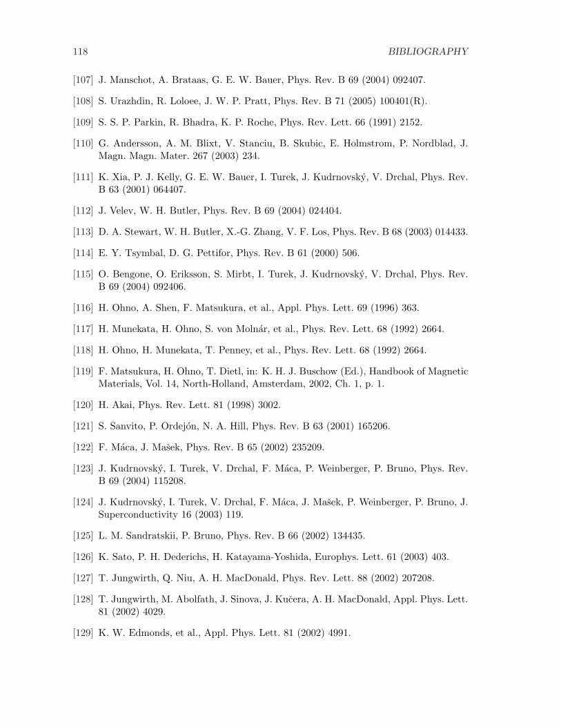
118 BIBLIOGRAPHY
[107] J. Manschot, A. Brataas, G. E. W. Bauer, Phys. Rev. B 69 (2004) 092407.
[108] S. Urazhdin, R. Loloee, J. W. P. Pratt, Phys. Rev. B 71 (2005) 100401(R).
[109] S. S. P. Parkin, R. Bhadra, K. P. Roche, Phys. Rev. Lett. 66 (1991) 2152.
[110] G. Andersson, A. M. Blixt, V. Stanciu, B. Skubic, E. Holmstrom, P. Nordblad, J.Magn. Magn. Mater. 267 (2003) 234.
[111] K. Xia, P. J. Kelly, G. E. W. Bauer, I. Turek, J. Kudrnovsky, V. Drchal, Phys. Rev.B 63 (2001) 064407.
[112] J. Velev, W. H. Butler, Phys. Rev. B 69 (2004) 024404.
[113] D. A. Stewart, W. H. Butler, X.-G. Zhang, V. F. Los, Phys. Rev. B 68 (2003) 014433.
[114] E. Y. Tsymbal, D. G. Pettifor, Phys. Rev. B 61 (2000) 506.
[115] O. Bengone, O. Eriksson, S. Mirbt, I. Turek, J. Kudrnovsky, V. Drchal, Phys. Rev.B 69 (2004) 092406.
[116] H. Ohno, A. Shen, F. Matsukura, et al., Appl. Phys. Lett. 69 (1996) 363.
[117] H. Munekata, H. Ohno, S. von Molnar, et al., Phys. Rev. Lett. 68 (1992) 2664.
[118] H. Ohno, H. Munekata, T. Penney, et al., Phys. Rev. Lett. 68 (1992) 2664.
[119] F. Matsukura, H. Ohno, T. Dietl, in: K. H. J. Buschow (Ed.), Handbook of MagneticMaterials, Vol. 14, North-Holland, Amsterdam, 2002, Ch. 1, p. 1.
[120] H. Akai, Phys. Rev. Lett. 81 (1998) 3002.
[121] S. Sanvito, P. Ordejon, N. A. Hill, Phys. Rev. B 63 (2001) 165206.
[122] F. Maca, J. Masek, Phys. Rev. B 65 (2002) 235209.
[123] J. Kudrnovsky, I. Turek, V. Drchal, F. Maca, P. Weinberger, P. Bruno, Phys. Rev.B 69 (2004) 115208.
[124] J. Kudrnovsky, I. Turek, V. Drchal, F. Maca, J. Masek, P. Weinberger, P. Bruno, J.Superconductivity 16 (2003) 119.
[125] L. M. Sandratskii, P. Bruno, Phys. Rev. B 66 (2002) 134435.
[126] K. Sato, P. H. Dederichs, H. Katayama-Yoshida, Europhys. Lett. 61 (2003) 403.
[127] T. Jungwirth, Q. Niu, A. H. MacDonald, Phys. Rev. Lett. 88 (2002) 207208.
[128] T. Jungwirth, M. Abolfath, J. Sinova, J. Kucera, A. H. MacDonald, Appl. Phys. Lett.81 (2002) 4029.
[129] K. W. Edmonds, et al., Appl. Phys. Lett. 81 (2002) 4991.
BIBLIOGRAPHY 119
[130] I. Turek, J. Kudrnovsky, V. Drchal, P. Weinberger, J. Phys.: Condens. Matter 16(2004) S5607.
[131] H. Ohno, J. Magn. Magn. Mater. 200 (1999) 110.
[132] J. Masek, J. Kudrnovsky, F. Maca, Phys. Rev. B 67 (2003) 153203.
[133] V. Drchal, J. Kudrnovsky, I. Turek, F. Maca, P. Weinberger, Phil. Mag. 84 (2004)1889.
[134] P. A. Korzhavyi, I. A. Abrikosov, E. A. Smirnova, L. Bergqvist, P. Mohn, R. Mathieu,P. Svendlindh, J. Sadowski, E. I. Isaev, Y. K. Vekhilov, O. Eriksson, Phys. Rev. Lett.88 (2002) 187202.
[135] I. Turek, K. Carva, J. Kudrnovsky, Transport properties of (Ga,Mn)As diluted mag-netic semiconductors in the bulk and in layered systems, Adv. Sci. Tech. 52 (2006)1.
[136] D. Chiba, F. Matsukura, H. Ohno, Physica E 21 (2004) 966.
[137] K. Carva, I. Turek, Ab initio calculations of transport properties of epitaxial(Ga,Mn)As systems, accepted for publication in J. Magn. Magn. Mater.
[138] J. Kudrnovsky, V. Drchal, F. Maca, I. Turek, G. Bouzerar, P. Bruno, in: P. E. A.Turchi, A. Gonis, K. Rajan, A. Meike (Eds.), Complex Inorganic Solids – Structural,Stability, and Magnetic Properties of Alloys, Springer, New York, 2005, p. 277.
[139] S. Ishida, T. Masaki, S. Fujii, S. Asano, Physica B 245 (1998) 1.
[140] Y. Sakuraba, M. Hattori, M. Oogane, Y. Ando, H. Kato, et al., Appl. Phys. Lett. 88(2006) 192508.
[141] Y. Sakuraba, T. Miyakoshi, M. Oogane, Y. Ando, et al., Appl. Phys. Lett. 89 (2006)052508.
[142] S. Kammerer, The Heusler alloy Co2MnSi in thin films, Ph.D. thesis, UniversitatBielefeld (2004).
[143] P. Brown, K. Neumann, P. Webster, K. Ziebeck, J. Phys.: Condens. Matter 12 (2000)1827.
[144] L. Ritchie, G. Xiao, Y. Ji, T. Y. Chen, C. L. Chien, et al., Phys. Rev. B 68 (2003)104430.
[145] B. Ravel, M. P. Raphael, V. G. Harris, Q. Huang, Phys. Rev. B 65 (2001) 184431.
[146] T. Marukame, H. Kijima, T. Ishikawa, K. i. Matsuda, T. Uemura, M. Yamamoto,submitted to J. Magn. Magn. Mater.
[147] Y. Sakuraba, et al., Jpn. J. Appl. Phys. 44 (2005) L1100.
[148] J. Masek, J. Kudrnovsky, F. Maca, B. L. Gallagher, et al., preprint: cond-mat/0609184, submitted to Phys. Rev. Lett.