spd file format - bbs.hwrf.com.cnbbs.hwrf.com.cn/downpcbe/spd_file_format_rg-3212.pdf · table of...
TRANSCRIPT
S I G R I T Y I N C O R P O R A T E D
R E F E R E N C E G U I D E
.spd File Format

Copyright © 2011 Sigrity, Inc. All Rights Reserved.900 E. Hamilton Avenue, Suite 500, Campbell, CA 95008
Printed in the United States of America.
Trademark: SpeedXP, SPEED2000, PowerSI, Broadband SPICE, PowerDC, SpeedPKG, XtractIM, SpeedPCB, OptimizePI, Unified Package Designer, OrbitIO, Channel Designer and other Sigrity Product names referenced therein are trademarks of Sigrity, Inc. and may be registered in certain jurisdictions.
All other products, designations, logos, and symbols mentioned in this manual are used for identification purposes only, and may be trademarks or registered trademarks of their respective companies. Registered and unregistered trademarks, as used in this manual, are the exclusive property of their respective owners.
Restricted Permission: This publication contains trade secrets and proprietary information owned by Sig-rity and is protected by copyright law. Unauthorized reproduction or distribution of this publication, or any portion of it, may result in civil and criminal penalties. This publication may not be copied, reproduced, modified, published, uploaded, posted, transmitted, or distributed outside of Sigrity in any way, without prior written permission from Sigrity. Except as specified in this permission statement, which grants Sigrity customers permission to print hard copies of this publication subject to the following conditions:
1. Any authorized copy of the publication or portion thereof must include all original copyright, trademark and other proprietary notices and this permission statement.
2. The publication may not be modified in any way.3. The information contained in this document shall not be used for the benefit of any third party.
SpeedXP Suite Release 11.1
Last Updated: 11/28/11
I
Table of Contents .spd File Format Reference Guide 11.1
Table of Contents1 Introduction........................................................................................... 1
What is .spd File Format?....................................................................................................... 1Additional Documentation ............................................................................................... 2
Conventions Used in this Guide ............................................................................................. 2Contact Us ........................................................................................................................ 2
2 General Format of .spd Files................................................................. 3.spd File Sections.................................................................................................................... 3Default Units .......................................................................................................................... 4
Scale Factors..................................................................................................................... 5Naming Conventions .............................................................................................................. 5Line Types .............................................................................................................................. 5
Title Line .......................................................................................................................... 5Comment Line .................................................................................................................. 5.End Line .......................................................................................................................... 5
General Form for End Lines ....................................................................................... 6Trace reference check............................................................................................................. 6
3 Global Parameter Lines......................................................................... 7Global Parameter Descriptions............................................................................................... 7
4 Computation Parameter Lines .............................................................. 9.Transient Line........................................................................................................................ 9
Transient Line Parameter Descriptions..................................................................... 10.Mesh Line............................................................................................................................ 12
Mesh Line Parameter Descriptions........................................................................... 12.TEMP Line .......................................................................................................................... 12.MaterialFileName Line ....................................................................................................... 12
5 Package Shape and Layout Description Lines................................... 13The Package Commands ...................................................................................................... 13
Package Parameter Descriptions............................................................................... 14Package Shape Description Lines ........................................................................................ 15
The Shape Command...................................................................................................... 15Shape Parameter Descriptions .................................................................................. 15
Box Parameter ................................................................................................................ 16Box Parameter Descriptions ..................................................................................... 16
Polygon Parameter.......................................................................................................... 17Polygon Parameter Descriptions............................................................................... 17
Circle Parameter ............................................................................................................. 18Circle Parameter Descriptions .................................................................................. 18
UnionizedShape Line ..................................................................................................... 19Package Layout Description Lines....................................................................................... 19
Package Layout Description Lines ........................................................................... 20Plane Layer Description Line ......................................................................................... 20
I I
.spd File Format Reference Guide 11.1
Plane Layer Parameter Descriptions..........................................................................22Signal Layer Description Line ..............................................................................................23
Signal Layer Parameter Descriptions ........................................................................23SPD File Format Parameter Descriptions..................................................................24
Medium Description Line ...............................................................................................25Medium Parameter Descriptions ...............................................................................26
Patch Description Line ....................................................................................................28Patch Parameter Descriptions....................................................................................29
Trace Surface Roughness Description Lines ........................................................................30Trace Surface Roughness Parameter Descriptions ....................................................30
Padstack Description Line.....................................................................................................30The Padstack Commands ................................................................................................31
Padstack Parameter Descriptions...............................................................................31The PadDef Commands...................................................................................................31
PadDef Parameter Descriptions.................................................................................33Material Description Lines....................................................................................................34
Specify Material Model...................................................................................................34Material Model Parameter Descriptions....................................................................35
Node Description Line ..........................................................................................................36Node Parameter Descriptions ....................................................................................37
Via Description Line .............................................................................................................38Via Parameter Descriptions .......................................................................................39
Wirebond Description Lines .................................................................................................40Wirebond Example 1.......................................................................................................40Wirebond Example 2......................................................................................................41
Wirebond Parameter Descriptions.............................................................................41Wirebond Models ............................................................................................................42
Four Point Model.......................................................................................................42Five Point Model .......................................................................................................42Reverse 4-Point Model ..............................................................................................42The K&S Standard Model .........................................................................................43The K&S Loop Model ...............................................................................................43The Cadence Discrete Model ....................................................................................44
WirebondGroup Description Lines .......................................................................................45WirebondGroup Parameter Descriptions...................................................................45
Trace Description Line..........................................................................................................46Trace Parameter Descriptions....................................................................................47
ClippedTrace Line.................................................................................................................48Segmented Trace Line...........................................................................................................48CPL Description Line ...........................................................................................................48
CPL Parameter Descriptions .....................................................................................48GCPL Description Block.................................................................................................49
GCPL Illustration ......................................................................................................49GCPL Parameter Descriptions...................................................................................50
Lead Description Lines .........................................................................................................50Lead Parameter Descriptions.....................................................................................52
LeadGroup Description Lines .........................................................................................54LeadGroup Parameter Descriptions...........................................................................54
6 Circuit Component Description Lines................................................. 55

I I I
Table of Contents .spd File Format Reference Guide 11.1
Partial Circuit Network ........................................................................................................ 55Circuit Component Description Lines ............................................................................ 55
Circuit Component Parameter Descriptions ............................................................. 56Arbitrary Mathematical Expression Processing ................................................................... 57
Mathematical Expressions .............................................................................................. 58Voltage Variables ........................................................................................................... 59Current Variable ............................................................................................................. 59Parameters in Mathematical Expressions ....................................................................... 60Values of G and E Components ..................................................................................... 60
G and E Parameter Descriptions ............................................................................... 61Values of R, L, and C Components ................................................................................ 62
R, L, and C Component Parameter Descriptions...................................................... 62Parameter Names.................................................................................................................. 63Global Parameters (.Param) ................................................................................................. 64Local Parameters .................................................................................................................. 64
Local Parameter Descriptions......................................................................................... 65Partial Circuit Command...................................................................................................... 66
Nested Sub circuit Definition ......................................................................................... 67Partial Circuit Parameter Descriptions ........................................................................... 69
.Connect - Circuit Package Connection Lines...................................................................... 70Circuit Package Connection Parameters......................................................................... 70
.Model Description Line....................................................................................................... 71Model Parameter Descriptions.................................................................................. 71Capacitor Parameter Descriptions............................................................................. 72Diode Parameter Descriptions .................................................................................. 73MOSFET Level 1 Parameter Descriptions ............................................................... 76Resistor Parameter Descriptions ............................................................................... 77Small Signal Parameter Data Frequency Table Model (SP Model) ......................... 78Coupled Transmission Lines Parameters for ModelType W.................................... 79Tabular W Model...................................................................................................... 80S Parameter Descriptions.......................................................................................... 80Bulk to Source / Drain Diodes - DC Part Parameters............................................... 81Bulk to Source / Drain Diodes - Capacitance Part Parameters................................. 82Drain and Source Resistance Parameters.................................................................. 83Gate Capacitances Parameters .................................................................................. 84Effective Length and Width Parameters ................................................................... 85Threshold Voltage Parameters.................................................................................. 86Impact Ionization Parameters ................................................................................... 87Temperature Effects Parameters ............................................................................... 87
MOSFET BSIM 3 v3 Level 49 / 53 ..................................................................................... 88BSIM3 v3 Specific Element Parameter Descriptions............................................... 89BSIM3 v3 Model Selector Parameter Descriptions.................................................. 89BSIM3 v3 ACM-0, 1, 2, 3 Parameter Descriptions.................................................. 90BSIM3v3 STI / LOD Model Parameter Descriptions............................................... 91
MOSFET BSIM4 Level 54 .................................................................................................. 92BSIM4 Specific Element Parameter Descriptions.................................................... 93Additional BSIM4 Model Parameters in SPDSIM................................................... 94
Subcircuit Command............................................................................................................ 94Nested Subcircuit Definition .......................................................................................... 96Subcircuit Parameter Definitions.................................................................................... 98GC - Capacitor Description Line.................................................................................... 98

I V
.spd File Format Reference Guide 11.1
Capacitor Parameters .................................................................................................99_Cmatrix - Mutual Capacitor Matrix Description Line.................................................100
Mutual Capacitor Matrix Parameter Descriptions...................................................100D - Diode Description Line ...........................................................................................100
Diode Parameter Descriptions .................................................................................101E - Foster Pole-residue Form Gain Function.................................................................102
Trans-conductance Parameter Descriptions ............................................................102E - Laplace and Pole-zero Voltage Gain Function........................................................103
Using the Parameters ...............................................................................................103Voltage Gain Parameter Descriptions .....................................................................103
E – Voltage Controlled Voltage Source (VCVS)..........................................................104Delay........................................................................................................................104Linear.......................................................................................................................104Polynomial...............................................................................................................104Piecewise Linear......................................................................................................104Mathematic Expression ...........................................................................................104Multi-Input Gates ....................................................................................................105Transformer .............................................................................................................105Voltage Controlled Voltage Parameter Descriptions ..............................................105
F – Current Controlled Current Source (CCCS) ...........................................................107Delay........................................................................................................................107Linear.......................................................................................................................107Multi-Input Gates ....................................................................................................107Piecewise Linear......................................................................................................107Polynomial...............................................................................................................107CCCS Parameter Descriptions.................................................................................108
G - Foster Pole-residue Form Trans-conductance Function ........................................109Trans-conductance Parameter Descriptions ............................................................109
G - Laplace and Pole-zero Trans-conductance Function ..............................................110Laplace.....................................................................................................................110Pole ..........................................................................................................................110Using the Trans-conductance Parameters................................................................110Trans-conductance Parameter Descriptions ............................................................111
G – Voltage Controlled Capacitor (VCCAP)................................................................112Linear.......................................................................................................................112Mathematic Expression ...........................................................................................112Piecewise Linear......................................................................................................112Polynomial...............................................................................................................112VCCAP Parameter Descriptions .............................................................................113
G – Voltage Controlled Current Source (VCCS)..........................................................114Linear.......................................................................................................................114Delay........................................................................................................................114Mathematic Expression ...........................................................................................114Multi-Input Gates ....................................................................................................114Piecewise Linear......................................................................................................114Polynomial...............................................................................................................114VCCS Parameter Descriptions ................................................................................115
Mathematical Expressions.............................................................................................116G – Voltage Controlled Resistor (VCR) .......................................................................117
Linear.......................................................................................................................117Mathematic Expression ...........................................................................................117
V
Table of Contents .spd File Format Reference Guide 11.1
Multi-Input Gates.................................................................................................... 117Piecewise Linear ..................................................................................................... 117Polynomial .............................................................................................................. 117VCR Parameter Descriptions.................................................................................. 118
H – Current Controlled Voltage Source (CCVS) ......................................................... 119Linear ...................................................................................................................... 119Delay ....................................................................................................................... 119Multi-Input Gates.................................................................................................... 119Piecewise Linear ..................................................................................................... 119Polynomial .............................................................................................................. 119CCVS Parameter Descriptions................................................................................ 120
I - Current Source Description Line ............................................................................. 121Current Source Parameter Descriptions.................................................................. 121
K - Mutual Inductor Description Line .......................................................................... 122Mutual Inductor Parameter Descriptions ................................................................ 122
_Lmatrix - Inductor Matrix Description Line............................................................... 123Inductor Matrix Parameter Descriptions................................................................. 124Branch Parameter Descriptions............................................................................... 124
L - Inductor Description Line ....................................................................................... 124Inductor Parameter Descriptions............................................................................. 125
M - MOSFET Description Line.................................................................................... 125MOSFET Parameter Descriptions .......................................................................... 126
R - Resistor Description Line ....................................................................................... 127Resistor Parameter Descriptions ............................................................................. 128
S - S Parameters Description Line................................................................................ 129S Parameter Descriptions........................................................................................ 129
T - Transmission Line Description Line....................................................................... 130Transmission Parameter Descriptions..................................................................... 130
V - Voltage Source Description Line ........................................................................... 131Voltage Source Parameter Descriptions ................................................................. 131
W - Coupled Transmission Description Line ............................................................... 132Using the Coupled Transmission Parameters ......................................................... 132Coupled Transmission Parameter Descriptions ...................................................... 132
_X - Subcircuit Description Line.................................................................................. 133Subcircuit Parameter Descriptions.......................................................................... 133
Device Model Options (.Option) .................................................................................. 134Device Model Option Parameter Descriptions ....................................................... 134
Device Temperatures (.Temp) ...................................................................................... 135Mutual Capacitor Matrices ........................................................................................... 135
Mutual Capacitor Parameter Descriptions .............................................................. 136Transient Waveform Specifications ................................................................................... 137
Digital_PWL Waveform............................................................................................... 137Digital_PWL Waveform Parameter Descriptions .................................................. 138
Digital_Ramp Waveform ............................................................................................. 139Digital_Ramp Waveform Parameter Descriptions ................................................. 140
Digital_Sinesquare Waveform ..................................................................................... 141Digital_Sinesquare Waveform Parameter Descriptions ......................................... 142
Exponential Waveform................................................................................................. 143Exponential Waveform Parameter Descriptions..................................................... 143
Frequency-Modulated Waveform................................................................................. 144Waveform Amplitude ............................................................................................. 144

V I
.spd File Format Reference Guide 11.1
Frequency Modulated Waveform Parameter Descriptions .....................................144Gaussian Waveform ......................................................................................................145
Gaussian Waveform Parameter Descriptions ..........................................................145Piecewise Linear Waveform .........................................................................................146
Piecewise Linear Waveform Parameter Descriptions .............................................146Pulse Waveform ............................................................................................................147
Pulse Waveform Parameter Descriptions ................................................................147Waveform Amplitude Parameter Descriptions........................................................147
Sinesquare Waveform ...................................................................................................148Sinesquare Waveform Parameter Descriptions .......................................................148Waveform Amplitude Parameter Descriptions........................................................149
Sinusoidal Waveform ....................................................................................................150Sinusoidal Waveform Parameter Descriptions........................................................150Waveform Amplitude Parameter Descriptions........................................................150
Random Bits Waveform................................................................................................151Random Bits Waveform Parameter Descriptions....................................................152Examples of Source with Random Bits Waveform.................................................153
Partial Circuit And Package Connection Description Line...........................................154Partial Circuit and Package Connection Parameter Descriptions............................154
Polynomial Functions in Nonlinear Circuit Elements ........................................................155Bit Usage.............................................................................................................................156
7 Other General Description Lines ...................................................... 157Viewing Parameter Lines....................................................................................................157
.ViewCktVoltage Command Line.................................................................................157ViewCktVoltage Parameter Descriptions................................................................158
.ViewPkgVoltage Command Line ................................................................................158ViewPkgVoltage Parameter Descriptions ...............................................................158
.ViewCurrent Command Line .......................................................................................159ViewCurrent Parameter Descriptions......................................................................159
.View3D Command Line ..............................................................................................159View3D Parameter Descriptions .............................................................................160
.Distribution Command Line.........................................................................................161Distribution Parameter Descriptions .......................................................................161
Output Parameter Lines.......................................................................................................161.Output3DVoltage Command Line ..............................................................................161
Output3DVoltage Parameter Descriptions ..............................................................162.Output3DCurrent Command Line................................................................................162
Output3DCurrent Parameter Descriptions...............................................................163Net Management Lines .......................................................................................................164
NetList Statement ..........................................................................................................164NetList Parameter Descriptions...............................................................................164
UNIX Window Parameter Lines.........................................................................................165UNIX Parameter Descriptions.................................................................................166
8 PowerSI Formats ............................................................................... 167S-Element............................................................................................................................167
S - Element Parameter Descriptions..............................................................................168.PowerSI Commands...........................................................................................................168Source Types.......................................................................................................................168

V I I
Table of Contents .spd File Format Reference Guide 11.1
Random Bits ................................................................................................................. 168Source Netlists ........................................................................................................ 168
Section Lines ...................................................................................................................... 169.FrequencySweep.......................................................................................................... 170
FrequencySweep Parameter Descriptions............................................................... 171.Port Commands ................................................................................................................. 172
Portxxxx Parameter Descriptions ................................................................................. 172.DiffChannels Commands .................................................................................................. 173
Diff_Channel_xxxx_$_yyyy Parameter Descriptions.................................................. 173Transient Waveform Specifications ................................................................................... 174
Frequency Piecewise Linear Waveform Parameter Descriptions ................................ 174
9 Speed2000 Format ............................................................................ 175SPEED2000 COMMANDS ............................................................................................... 175
Examples ...................................................................................................................... 175Description Lines.......................................................................................................... 176
.Mode description line ............................................................................................ 176
.TDR description line.............................................................................................. 176
.SSO description line .............................................................................................. 177I/O Buffer Information Specification (IBIS)...................................................................... 177
Supported Keywords .................................................................................................... 178Random Bits ................................................................................................................. 179
Source Netlists ........................................................................................................ 179IBIS Statements ............................................................................................................ 179
IBIS Parameter Descriptions................................................................................... 180IBIS Input Buffer.......................................................................................................... 182
IBIS Input Buffer Illustration ................................................................................. 183IBIS Input Buffer Parameter Descriptions.............................................................. 184
IBIS Output Buffer ....................................................................................................... 185Output Buffer Illustration ....................................................................................... 185IBIS Output Buffer Parameter Descriptions ........................................................... 186
IBIS Tristate Buffer ...................................................................................................... 187IBIS Tristate Buffer Illustration.............................................................................. 187IBIS Tristate Buffer Parameter Descriptions.......................................................... 188
IBIS I/O Buffer ............................................................................................................. 189I/O Buffer Illustration ............................................................................................. 189IBIS I/O Buffer Parameter Descriptions................................................................. 190
IBIS Open Drain Buffer ............................................................................................... 191IBIS Open Drain Buffer Illustration ....................................................................... 191IBIS Open Drain Buffer Parameter Descriptions ................................................... 192
IBIS I/O Open Drain Buffer ......................................................................................... 192IBIS I/O Open Drain Buffer Illustration................................................................. 193IBIS I/O Open Drain Buffer Parameter Descriptions ............................................. 194
IBIS Open Sink Buffer ................................................................................................. 195IBIS Open Sink Buffer Parameter Descriptions ..................................................... 196
IBIS I/O Open Sink Buffer ........................................................................................... 196IBIS I/O Open Sink Buffer Illustration................................................................... 197IBIS I/O Open Sink Buffer Parameter Descriptions............................................... 197
IBIS Open Source Buffer ............................................................................................. 198IBIS Open Source Buffer Illustration ..................................................................... 198

V I I I
.spd File Format Reference Guide 11.1
IBIS Open Source Buffer Parameter Descriptions ..................................................199IBIS I/O Open Source Buffer ........................................................................................200
IBIS I/O Open Source Buffer Illustration................................................................200IBIS I/O Open Source Buffer Parameter Descriptions............................................201
IBIS Input ECL Buffer .................................................................................................202IBIS Input ECL Buffer Illustration..........................................................................202IBIS Input ECL Buffer Parameter Descriptions......................................................203
IBIS Output ECL Buffer ...............................................................................................203IBIS Out ECL Buffer Illustration ............................................................................204IBIS Output ECL Buffer Parameter Descriptions ...................................................204
IBIS Tristate ECL Buffer ..............................................................................................205IBIS Tristate ECL Buffer Illustration......................................................................205IBIS Tristate ECL Buffer Parameter Descriptions ..................................................206
IBIS I/O ECL Buffer ....................................................................................................207IBIS I/O ECL Buffer Illustration.............................................................................207IBIS I/O ECL Buffer Parameter Descriptions.........................................................208
IBIS Terminator Buffer .................................................................................................209IBIS Terminator Buffer Illustration.........................................................................209IBIS Terminator Buffer Parameter Descriptions.....................................................210
Series Models ......................................................................................................................211Series Switch Type........................................................................................................211
Series and Series Switch Buffer Parameter Descriptions........................................211IBIS Series Buffer .........................................................................................................211
IBIS Series Buffer Parameter Descriptions .............................................................212IBIS Series Switch Buffer .............................................................................................212
IBIS Series Switch Buffer Illustration.....................................................................212Add an Associated IBIS File...............................................................................................213
Data Selection for typ = fast / slow .............................................................................215Circuit Solvers.....................................................................................................................216
External Circuit Solver..................................................................................................216External Circuit Solver Parameter Descriptions......................................................216
.HSPICE Circuit Solvers ...............................................................................................216 .EndHSPICE.................................................................................................................216
Include Command Support .................................................................................................217Library Command Support .................................................................................................218
.LIB Command..............................................................................................................218
10 MOSFET BSIM3v3 Model Parameters ............................................... 219MOSFET BSIM3v3 Model Parameter Descriptions ..........................................................219
DC Parameters...............................................................................................................221AC Model Parameters .........................................................................................................225Geometry Parameters ..........................................................................................................227Temperature Parameters......................................................................................................229STI/LOD Model Parameters ...............................................................................................230
10 MOSFET BSIM4 Model Parameters ................................................... 231MOSFET Level 1 Parameter Descriptions .........................................................................231MOSFET BSIM4 (Level 54) Parameter Descriptions ........................................................232

I X
Table of Contents .spd File Format Reference Guide 11.1
Index...............................................................................249

X
.spd File Format Reference Guide 11.1

1
Chapter
1Introduction
This manual is designed to give you an introduction to the .spd file format used by Sigrity tools. The basic concepts and requirements are explained in detail. The goal is to aid you in your success using of a new type of power and signal integrity software tool.
WHAT IS .SPD FILE FORMAT?The .spd file is the native file format used by Sigrity products to provide the data, viewing and output parameters for simulation.
In most cases the same .spd file format works with both Speed2000 and PowerSI. A limited number of statements have meaning in either PowerSI or Speed2000 only.
Refer to Mesh Plane Emulation in Plane Layer Description Line for the special case when hand-editing is require
IMPORTANT!!
We recommend that you always introduce changes to the .spd file through use of our graphical editing tools: SPDGEN or PowerSI.
We recognize that some users choose to hand edit the.spd file, using text editors. It is for this reason that we have produced this document to provide descrip-tions of the .spd file format and options.

I N T R O D U C T I O N 2
Conventions Used in this Guide .spd File Format Reference Guide 11.1
Additional DocumentationIn addition to this manual, refer to the following documentation for more information.
• PowerSI Getting Started Guide
• PowerSI User Guide
• SPEED2000 Getting Started Guide
• SPEED2000 User’s Guide
CONVENTIONS USED IN THIS GUIDE
Contact UsSigrity is committed to helping you in using the Sigrity tools.
If you encounter any difficulties or if you have any suggestions for improvements, please let us know.
Contact us by:
• Phone: 408.688.0145
• FAX: 408.688.0144
• Email: [email protected]
• Web: www.sigrity.com
The latest edition of the PowerSI User Guide, new product information and product updates are posted on the website.
CONVENTION USE
Bold GUI text, special names, terms (window names, buttons, menus, etc.).
Ariel Examples.
> Menu hierarchy.

3
Chapter
2General Format of .spd Files
The .spd file is an ASCII formatted text file that can be read by text editors.
.SPD FILE SECTIONSAll .spd files contain similar sections and each section provides specific information. Many sections are delimited by specific taglines that begin and end the sections. The .spd data file contains the following types of lines:
• Circuit Component Description Lines• Circuit-Package Connection Lines• Comment Lines• Computation Parameter Lines• END Line• Net Management Lines• Package Shape and Layout Description Lines• PowerSI Lines• Title Line• Viewing and Output Parameter Lines• Window Parameter Lines (for UNIX systems now deprecated)
Any line except the first line can be a blank line. A line which is a continuation of the previous line is marked by the plus symbol (+) at the first column of the continued line and at least one blank space right after the symbol.
.SPD File ExampleThe comment lines may be located anywhere in the file except in the first line.
The order of the lines should be the same as the order shown in the demo-short.spd - Notepad example below.

G E N E R A L F O R M A T O F . S P D F I L E S 4
Default Units .spd File Format Reference Guide 11.1
DEFAULT UNITSThe following units are used within calculations:
The .spd file contents can be viewed and edited in word pro-cessors such as Notepad.
Admittance, Conductivity Meter
Ampere Ohm
Capacitance Resistance
Current Second
Farad Siemens
Henry Time
Inductance Volt
Length Voltage
G E N E R A L F O R M A T O F . S P D F I L E S 5
Naming Conventions .spd File Format Reference Guide 11.1
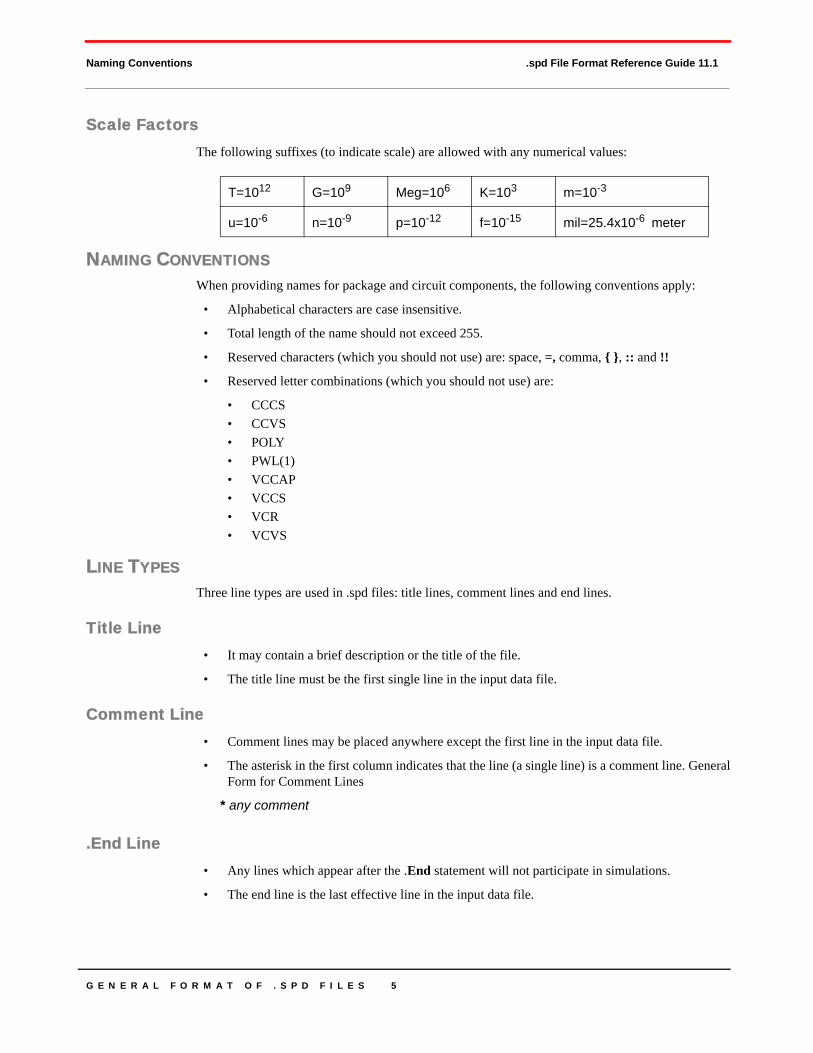
Scale FactorsThe following suffixes (to indicate scale) are allowed with any numerical values:
NAMING CONVENTIONSWhen providing names for package and circuit components, the following conventions apply:
• Alphabetical characters are case insensitive.
• Total length of the name should not exceed 255.
• Reserved characters (which you should not use) are: space, =, comma, { }, :: and !!
• Reserved letter combinations (which you should not use) are:
• CCCS• CCVS• POLY• PWL(1)• VCCAP• VCCS• VCR• VCVS
LINE TYPESThree line types are used in .spd files: title lines, comment lines and end lines.
Title Line• It may contain a brief description or the title of the file.
• The title line must be the first single line in the input data file.
Comment Line• Comment lines may be placed anywhere except the first line in the input data file.
• The asterisk in the first column indicates that the line (a single line) is a comment line. General Form for Comment Lines
* any comment
.End Line• Any lines which appear after the .End statement will not participate in simulations.
• The end line is the last effective line in the input data file.
T=1012 G=109 Meg=106 K=103 m=10-3
u=10-6 n=10-9 p=10-12 f=10-15 mil=25.4x10⁻⁶ meter
G E N E R A L F O R M A T O F . S P D F I L E S 6
Trace reference check .spd File Format Reference Guide 11.1
General Form for End Lines.End
End Line ExampleLines that begin
Backupshape
BackupUnionizedShape
and
.EndShape
have purposes related to backing up information and NET operations.
TRACE REFERENCE CHECK• If Trace Reference Check is set As Warning (Default setting), then the current .spd file
header is not changed.
• If Trace Reference Check is set As Error, then the line shown in the example is added to the .spd file header.
Trace Reference Check ExampleTitle - PowerSI file for version 2000.09
*Please do NOT edit special void criteria manually..DoglegHoleThreshold = 0.001500.ThermalHoleThreshold = 0.001500.SmallHoleThreshold = 0.00300.ViaHoleThreshold = 0.001500.TraceReference Check

7
Chapter
3Global Parameter Lines
The Global Parameter Lines specify the global simulation parameters.
GLOBAL PARAMETER DESCRIPTIONS
PARAMETER EFFECT OR MEANING
.DoglegHole Threshold Minimum Threshold below which Dogleg Hole is converted to a Special Void during Shape processing.
.ThermalHole Threshold Minimum Threshold below which Thermal Hole is converted to Special Void during Shape processing.
.SmallHole Threshold Minimum Threshold below which Small Hole is converted to Special Void during Shape processing.
.ViaHole Threshold Minimum Threshold below which Via Hole is converted to Special Void dur-ing Shape processing.
.ViaAntipadeSearchFactor These factors are used to create the missing Antipads during Shape pro-cessing.
First, all the edges whose shortest distance from the Via center is> (Via-Antipad DistanceRangeFactor = 1.1) x shortest distance.Then, average the sum of the shortest distances for remaining edges to get an average distance value. It is then used to create the Antipad Shape.
Users can change the Via Antipad search factor and the Via-Antipad Dis-tanceRangeFactor settings to create Antipads for more Vias that do not get covered with the default settings.
.ViaAntipadDistanceRangeFac-tor
G L O B A L P A R A M E T E R L I N E S 8
Global Parameter Descriptions .spd File Format Reference Guide 11.1
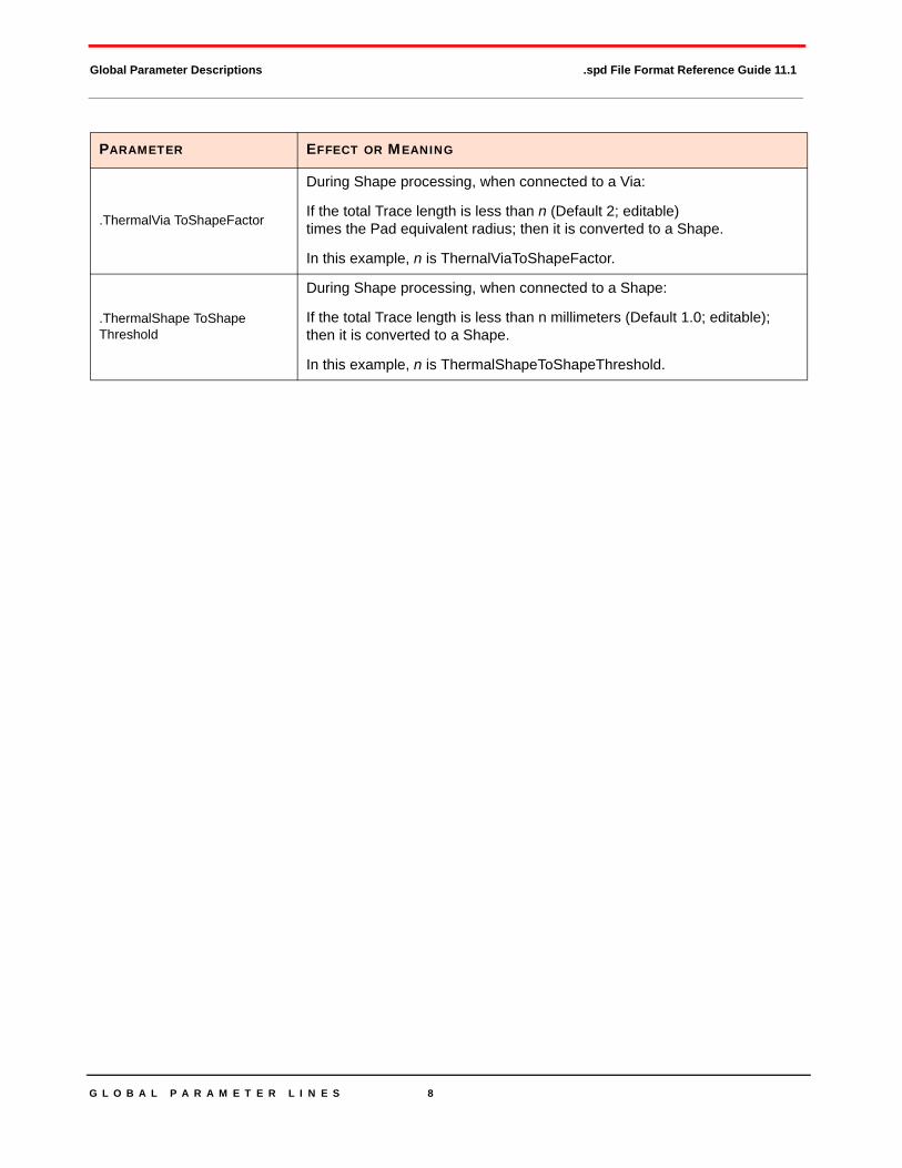
.ThermalVia ToShapeFactor
During Shape processing, when connected to a Via:
If the total Trace length is less than n (Default 2; editable) times the Pad equivalent radius; then it is converted to a Shape.
In this example, n is ThernalViaToShapeFactor.
.ThermalShape ToShape Threshold
During Shape processing, when connected to a Shape:
If the total Trace length is less than n millimeters (Default 1.0; editable);then it is converted to a Shape.
In this example, n is ThermalShapeToShapeThreshold.
PARAMETER EFFECT OR MEANING
9
Chapter
4Computation Parameter Lines
The computation parameter lines specify the overall simulation parameters.
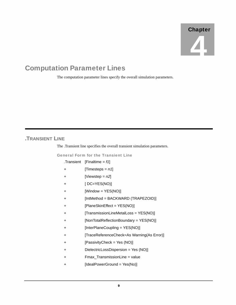
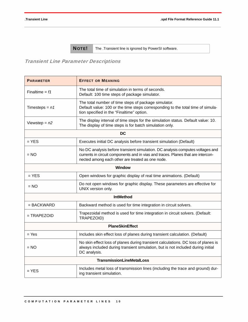
.TRANSIENT LINEThe .Transient line specifies the overall transient simulation parameters.
General Form for the Transient Line.Transient [Finaltime = f1]
+ [Timesteps = n1]
+ [Viewstep = n2]
+ [ DC=YES(NO)]
+ [Window = YES(NO)]
+ [IntMethod = BACKWARD (TRAPEZOID)]
+ [PlaneSkinEffect = YES(NO)]
+ [TransmissionLineMetalLoss = YES(NO)]
+ [NonTotalReflectionBoundary = YES(NO)]
+ [InterPlaneCoupling = YES(NO)]
+ [TraceReferenceCheck=As Warning(As Error)]
+ [PassivityCheck = Yes (NO)]
+ DielectricLossDispersion = Yes (NO)]
+ Fmax_TransmissionLine = value
+ [IdealPowerGround = Yes(No)]
C O M P U T A T I O N P A R A M E T E R L I N E S 1 0
.Transient Line .spd File Format Reference Guide 11.1
Transient Line Parameter Descriptions
NOTE! The .Transient line is ignored by PowerSI software.
PARAMETER EFFECT OR MEANING
Finaltime = f1 The total time of simulation in terms of seconds. Default: 100 time steps of package simulator.
Timesteps = n1The total number of time steps of package simulator.Default value: 100 or the time steps corresponding to the total time of simula-tion specified in the “Finaltime” option.
Viewstep = n2 The display interval of time steps for the simulation status. Default value: 10. The display of time steps is for batch simulation only.
DC
= YES Executes initial DC analysis before transient simulation (Default)
= NONo DC analysis before transient simulation. DC analysis computes voltages and currents in circuit components and in vias and traces. Planes that are intercon-nected among each other are treated as one node.
Window
= YES Open windows for graphic display of real time animations. (Default)
= NO Do not open windows for graphic display. These parameters are effective for UNIX version only.
IntMethod
= BACKWARD Backward method is used for time integration in circuit solvers.
= TRAPEZOID Trapezoidal method is used for time integration in circuit solvers. (Default: TRAPEZOID)
PlaneSkinEffect
= Yes Includes skin effect loss of planes during transient calculation. (Default)
= NONo skin effect loss of planes during transient calculations. DC loss of planes is always included during transient simulation, but is not included during initial DC analysis.
TransmissionLineMetalLoss
= YES Includes metal loss of transmission lines (including the trace and ground) dur-ing transient simulation.

C O M P U T A T I O N P A R A M E T E R L I N E S 1 1
.Transient Line .spd File Format Reference Guide 11.1
= NONo metal loss of transmission lines during the transient simulation. Transmis-sion lines are modeled as lossless transmission lines.(Default)
NonTotalReflectionBoundary
= YES Natural boundary (non-total reflection) condition at shape edges is used during simulation. (Default)
= NO Magnetic wall (total reflection) condition at shape edges is used during simula-tion.
InterplanePlaneCoupling
= YES Inter plane coupling will be taken into account in simulation. (Default)
= NO Inter plane coupling will be ignored in simulation.
PassivityCheck
= YESA more stable and slower scheme will be used for the extraction of transmis-sion line parameters for modeling the skin effect loss and/or dielectric loss. The passivity of the transmission model is checked.
= NO The passivity of the transmission line model is not checked for lines modeled with skin effect loss and/or dielectric loss. (Default)
DielectricLossDispersion
= YES Dielectric loss and dispersion will be considered in transient simulations for parallel-plate fields and transmission lines.
= NO Dielectric will be considered lossless and non-dispersive. If the dielectric con-stant is provided by a data file, the data at 1 GHz will be used. (Default)
Fmax_TransmissionLine
The frequency-dependency of the conductor loss and dielectric loss in the transient transmission line simulation is considered in the range from zero to Fmax_TransmissionLine. Default: 5GHz.
IdealPowerAndGround
= Yes The power and ground nets are ideal in simulation.
= NO Do not apply ideal power and ground nets in simulation. Default.
PARAMETER EFFECT OR MEANING
C O M P U T A T I O N P A R A M E T E R L I N E S 1 2
.Mesh Line .spd File Format Reference Guide 11.1
.MESH LINEThe Mesh description line specifies the mesh density used for numerical discretization and calcula-tions.
General Form for the Mesh Line.Mesh Pkg = s1 Mesh_X = n1 Mesh_Y = n2
Mesh Line Parameter Descriptions
.TEMP LINEThe Temp description line specifies the temperature used for the device model calculation and the met-al material conductivity calculation.
General Form for the Temp Line.Temp temperature_value
.MATERIALFILENAME LINEThe MaterialFileName description line specifies the material file name.
General Form for the MaterialFileName Line.MaterialFileName “path / material_file_name”
PARAMETER EFFECT OR MEANING
Pkg = s1 Name of the package or board.
Mesh_X =n1 Number of mesh elements in the x direction.(Default=60).
Mesh_Y =n2 Number of mesh elements in the y direction.(Default=60).
NOTE!If only Mesh_X is specified, Mesh_Y is set automatically so that dx=dy; and vice versa;
where dx= mesh length in the x direction and dy = mesh length in the y direction of a cartesian coordinate system.

13
Chapter
5Package Shape and Layout Description Lines
The Package Shape and Layout section of the .spd file starts with the command .Package and ends with the command .EndPackage.
THE PACKAGE COMMANDS
General Form for .Package Command.Package PackageName [Trace_Color = s1] [ Via_Color = s2] [ Hole_Color = s3]
+ [Top_Mesh_Color = s4] [Whole_Mesh_Color = s5]
+ [Plane_Color = s6] [Trace_Combine=YES(NO)]
+ [Fdtdthickness=YES(NO)] [r_default=f1]
+ via_conductivity_default

P A C K A G E S H A P E A N D L A Y O U T D E S C R I P T I O N L I N E S 1 4
The Package Commands .spd File Format Reference Guide 11.1
Package Parameter Descriptions
General Form.EndPackage
PARAMETER EFFECT OR MEANING
PackageName A character string for the name of the package or board structure.
Trace_Color = s1 s1 is the name of the color for displaying Traces.Default color: white.
Via_Color = s2 s2 is the name of the color for displaying Vias. Default: white.
Hole_Color = s3 s3 is the name of the color for displaying Via holes.Default color: white.
Top_Mesh_Color = s4 s4 is the name of the color for displaying numerical mesh for the top plane. Default color: white.
Whole_Mesh_Color = s5 s5 is the name of the color for displaying the whole numerical mesh for the structure. Default color: white.
Plane_Color = s6 s6 is the name of the color for displaying planes.Default color: white.
Trace_Combine
= YES Combines multi-segment traces to a single transmission line if there is no branch.
= NO Does not combine multi-segment traces to a single transmission line. Default.
Fdtdthickness
= YES The thickness of traces is taken into account for field computation between planes. (Default)
= NO The thickness of traces is not taken into account.
Via_Conductivity_DefaultDefault value used in computations that require Via conductivity when the con-ductivity is not specified in the Via description line. Default: 5.8e+7
Via_Material_DefaultSpecify a default material for Vias. You can use either this setting or Via_Conductivity_Default but, not both. If this setting is not specified, default conductivity is not used.
NOTE!The conductivity parameter in this command is an optional value. If it is omitted, the Via_Conductivity_Default parameter value of the .Pack-age command is used.

P A C K A G E S H A P E A N D L A Y O U T D E S C R I P T I O N L I N E S 1 5
Package Shape Description Lines .spd File Format Reference Guide 11.1
PACKAGE SHAPE DESCRIPTION LINESShape description lines specify Shapes of objects on plane or signal layers. Types of shapes include box, polygon and circle. Each shape has a specific syntax specification detailed in this section.
The Shape Description Line section begins with the command .Shape and ends with the command .EndShape.
You can specify the following shapes:
• Box Parameter• Circle Parameter• Polygon Parameter• UnionizedShape Line
The Shape CommandThe Shape Description Line section begins with the command .Shape and ends with the command .EndShape.
General Form.Shape ShapeName [Color = s1]
General Form.EndShape
Shape Command Example.Shape Shape002 Color = green
Box8Zgx34::VSS- -6.600000e+000mm -6.600000e+000mm 1.320000e+001mm
+ 1.320000e+001mm
.EndShape
Shape Parameter Descriptions
PARAMETER EFFECT OR MEANING
.Shape Keyword for shape line.
ShapeName A character string for the name of the shape.
Color = s1 Name of color for drawing the shape.Default: white.
P A C K A G E S H A P E A N D L A Y O U T D E S C R I P T I O N L I N E S 1 6
Package Shape Description Lines .spd File Format Reference Guide 11.1
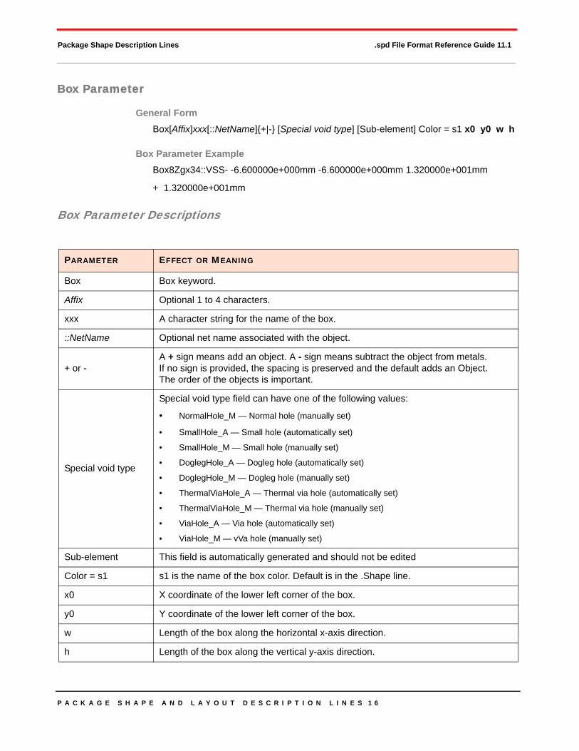
Box Parameter
General FormBox[Affix]xxx[::NetName]{+|-} [Special void type] [Sub-element] Color = s1 x0 y0 w h
Box Parameter ExampleBox8Zgx34::VSS- -6.600000e+000mm -6.600000e+000mm 1.320000e+001mm
+ 1.320000e+001mm
Box Parameter Descriptions
PARAMETER EFFECT OR MEANING
Box Box keyword.
Affix Optional 1 to 4 characters.
xxx A character string for the name of the box.
::NetName Optional net name associated with the object.
+ or -A + sign means add an object. A - sign means subtract the object from metals. If no sign is provided, the spacing is preserved and the default adds an Object. The order of the objects is important.
Special void type
Special void type field can have one of the following values:
• NormalHole_M — Normal hole (manually set)
• SmallHole_A — Small hole (automatically set)
• SmallHole_M — Small hole (manually set)
• DoglegHole_A — Dogleg hole (automatically set)
• DoglegHole_M — Dogleg hole (manually set)
• ThermalViaHole_A — Thermal via hole (automatically set)
• ThermalViaHole_M — Thermal via hole (manually set)
• ViaHole_A — Via hole (automatically set)
• ViaHole_M — vVa hole (manually set)
Sub-element This field is automatically generated and should not be edited
Color = s1 s1 is the name of the box color. Default is in the .Shape line.
x0 X coordinate of the lower left corner of the box.
y0 Y coordinate of the lower left corner of the box.
w Length of the box along the horizontal x-axis direction.
h Length of the box along the vertical y-axis direction.

P A C K A G E S H A P E A N D L A Y O U T D E S C R I P T I O N L I N E S 1 7
Package Shape Description Lines .spd File Format Reference Guide 11.1
Polygon Parameter
General FormPolygon[Affix]xxx[::NetName] [{+|-}] [Special void type] [Sub-element]Color = s1 x1 y1 x2 y2 ... xn yn
Polygon Parameter ExamplePolygon8Zgx01234::VSS -6.879373e+000mm -6.961050e+000mm6.868323e+000mm + -6.950000e+000mm 6.884824e+000mm -6.950000e+000mm 6.894257e+000mm + -6.961050e+000mm
Polygon Parameter Descriptions
PARAMETER EFFECT OR MEANING
Polygon Polygon key word.
Affix Optional 1 to 4 characters.
xxx A character string for the name of the polygon.
::NetName Optional net name associated with the object.
+ or - + sign means add object. - sign means subtract object from metals. If no sign, spacing is pre-served; default adds object. Order of objects is important.
Special void type
Special void type field can have one of the following values:
• NormalHole_M — Normal hole (manually set)
• SmallHole_A — Small hole (automatically set)
• SmallHole_M — Small hole (manually set)
• DoglegHole_A — Dogleg hole (automatically set)
• DoglegHole_M — Dogleg hole (manually set)
• ThermalViaHole_A — Thermal via hole (automatically set)
• ThermalViaHole_M — Thermal via hole (manually set)
• ViaHole_A — Via hole (automatically set)
• ViaHole_M — Via hole (manually set)
Sub-element This field is automatically generated and should not be edited.
Color = s1 s1 is the name of the box color. Default is specified in .Shape line.
x1 X coordinate of the first vertex of the polygon.
y1 Y coordinate of the first vertex of the polygon.
x2 X coordinate of the second vertex of the polygon.
y2 Y coordinate of the second vertex of the polygon.
xn X coordinate of the nth vertex of the polygon.
yn Y coordinate of the nth vertex of the polygon.
P A C K A G E S H A P E A N D L A Y O U T D E S C R I P T I O N L I N E S 1 8
Package Shape Description Lines .spd File Format Reference Guide 11.1
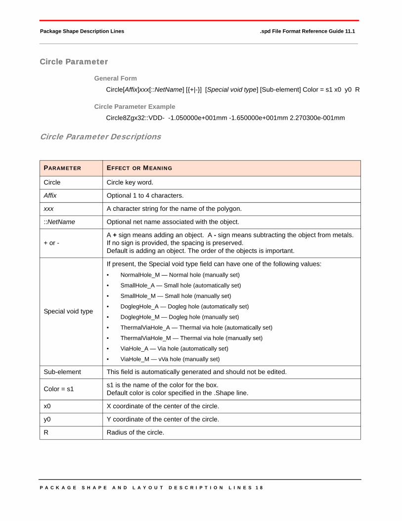
Circle Parameter
General FormCircle[Affix]xxx[::NetName] [{+|-}] [Special void type] [Sub-element] Color = s1 x0 y0 R
Circle Parameter ExampleCircle8Zgx32::VDD- -1.050000e+001mm -1.650000e+001mm 2.270300e-001mm
Circle Parameter Descriptions
PARAMETER EFFECT OR MEANING
Circle Circle key word.
Affix Optional 1 to 4 characters.
xxx A character string for the name of the polygon.
::NetName Optional net name associated with the object.
+ or -A + sign means adding an object. A - sign means subtracting the object from metals. If no sign is provided, the spacing is preserved. Default is adding an object. The order of the objects is important.
Special void type
If present, the Special void type field can have one of the following values: • NormalHole_M — Normal hole (manually set)
• SmallHole_A — Small hole (automatically set)
• SmallHole_M — Small hole (manually set)
• DoglegHole_A — Dogleg hole (automatically set)
• DoglegHole_M — Dogleg hole (manually set)
• ThermalViaHole_A — Thermal via hole (automatically set)
• ThermalViaHole_M — Thermal via hole (manually set)
• ViaHole_A — Via hole (automatically set)
• ViaHole_M — vVa hole (manually set)
Sub-element This field is automatically generated and should not be edited.
Color = s1 s1 is the name of the color for the box.Default color is color specified in the .Shape line.
x0 X coordinate of the center of the circle.
y0 Y coordinate of the center of the circle.
R Radius of the circle.
P A C K A G E S H A P E A N D L A Y O U T D E S C R I P T I O N L I N E S 1 9
Package Layout Description Lines .spd File Format Reference Guide 11.1
UnionizedShape LineUse the shape unionization procedure to add the following line in the .spd file after the Shape descrip-tions.
This line contains information used internally by the executable modules and it should not be altered by the user.
General FormUnionizedShape = s1
UnionizedShape Line ExampleUnionizedShape = 28545C0B-23545D13-23545515-2854550B
PACKAGE LAYOUT DESCRIPTION LINESPackage layout description lines specify properties of packaging components (listed below). They are placed after the Shape Description Lines.
General FormKeyword parameter1 parameter2 . . .
NOTE!The Plane, Medium and Signal layers should be placed strictly in top-to-bottom order as they appear in actual packages.
Plane and Signal layers have to be separated by medium layer(s).

P A C K A G E S H A P E A N D L A Y O U T D E S C R I P T I O N L I N E S 2 0
Package Layout Description Lines .spd File Format Reference Guide 11.1
Package Layout Description Lines
The order of the Layout Description Lines follows a logical hierarchy.
1. Layers (Plane or Medium or Signal and/or Patch).
2. Nodes that use those layers (to specify vertical placement.
3. Via and Trace (statements that use previously defined nodes).
4. CPL (after Traces that it uses).
5. GPL (after Traces that it uses).
Plane Layer Description LineSpeed2000 emulates the effects of mesh planes by making adjustments in the field solver module.
• Admittance• Capacitance• Inductance• Resistance parameters
Currently, entries for optional mesh plane emulation statement parameters must be introduced man-ually to the text file using a text editor.
Component Property
Plane Plane layers
Signal Signal layers
Medium Dielectric media
Patch Metal patch on signal layers
Node Labeling of specific locations in package
Via Vertical vias
Trace Horizontal traces
CPL Groups of coupled lines consisting of n single lines.
GCPL Groups of coupled lines consisting of n line series.
.Model Components such as diode.
IMPORTANT!! You must enter the additional information in all three description lines (patch, medium and signal).

P A C K A G E S H A P E A N D L A Y O U T D E S C R I P T I O N L I N E S 2 1
Package Layout Description Lines .spd File Format Reference Guide 11.1
General FormPlanexxxx thickness = f1 [Conductivity = f2 | Material = s1Shape = s2] [Color = s3]
+ [ AreaAdj=< ( [ X0 = f3 Y0 = f4 Xw = f5 Yw = f6 ]
+ [ Rxr = f7 ] [ Ryr = f8 ] ) ,
+ ( [ X0 = f9 Y0 = f10 Xw = f11 Yw = f12 ] [ Rxr = f13 ] [ Ryr = f14 ] ) ,
+ … > ]
Plane Layers Example 1 Plane$VCC Thickness = 3.560000e+001u Conductivity = 5.800000e+007 Shape = Shape001
+ Color = cyan
Plane Layers Example 2 Plane01 Thickness = 3.560000e+001u Conductivity = 5.800000e+007
+ Shape = Shape001 Color = cyan
+ AreaAdj=<
+ (X0 = 0 Y0 = 1 Xw = 3 Yw = 2
+ Rxr = 1.0 Ryr =4.0) ,
+ (X0 = -1 Y0 = -2 Xw = 4 Yw = 1
+ Rxr = 2.0 Ryr =3.0)
+ >
Plane Layers Example 3Plane01 Thickness = 3.560000e+001u Material = Copper
Plane Layers Example 4Plane$LYR_2 Thickness = 1.800000e-002mm Conductivity = 5.813953e+007 Shape = Shape$LYR_2 Color = magenta DoglegHole Threshold = 0.0015 ThermalHole Threshold = 0.0016 SmallHoleThreshold = 0.0015 ViaHole THreshold = 0.0015
X+
X-
X+Z
Y+
Y+
Y-
(X0, Y0)(f3, f4)
(0,0)
overlap
Xwf5
package origin
Ywf6
(X0, Y0)(f9, f10)
11f11XwXwXw
f12YYw
P A C K A G E S H A P E A N D L A Y O U T D E S C R I P T I O N L I N E S 2 2
Package Layout Description Lines .spd File Format Reference Guide 11.1
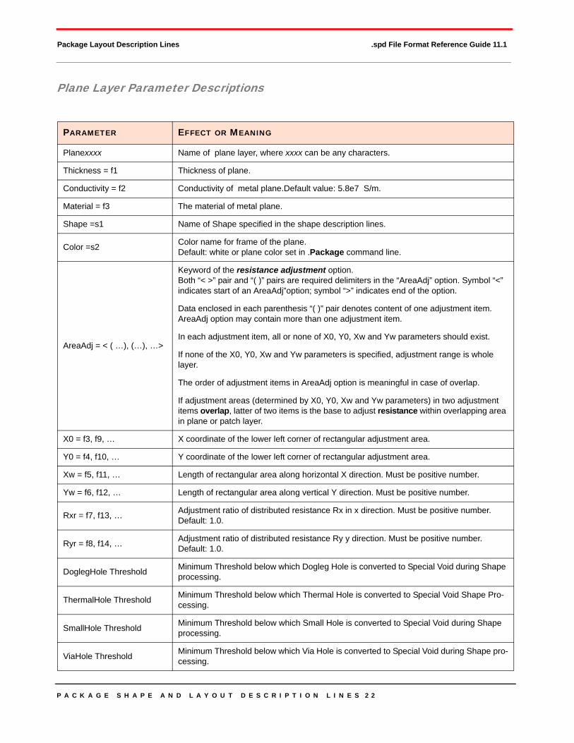
Plane Layer Parameter Descriptions
PARAMETER EFFECT OR MEANING
Planexxxx Name of plane layer, where xxxx can be any characters.
Thickness = f1 Thickness of plane.
Conductivity = f2 Conductivity of metal plane.Default value: 5.8e7 S/m.
Material = f3 The material of metal plane.
Shape =s1 Name of Shape specified in the shape description lines.
Color =s2 Color name for frame of the plane.Default: white or plane color set in .Package command line.
AreaAdj = < ( …), (…), …>
Keyword of the resistance adjustment option. Both “< >” pair and “( )” pairs are required delimiters in the “AreaAdj” option. Symbol “<” indicates start of an AreaAdj”option; symbol “>” indicates end of the option.
Data enclosed in each parenthesis “( )” pair denotes content of one adjustment item. AreaAdj option may contain more than one adjustment item.
In each adjustment item, all or none of X0, Y0, Xw and Yw parameters should exist.
If none of the X0, Y0, Xw and Yw parameters is specified, adjustment range is whole layer.
The order of adjustment items in AreaAdj option is meaningful in case of overlap.
If adjustment areas (determined by X0, Y0, Xw and Yw parameters) in two adjustment items overlap, latter of two items is the base to adjust resistance within overlapping area in plane or patch layer.
X0 = f3, f9, … X coordinate of the lower left corner of rectangular adjustment area.
Y0 = f4, f10, … Y coordinate of the lower left corner of rectangular adjustment area.
Xw = f5, f11, … Length of rectangular area along horizontal X direction. Must be positive number.
Yw = f6, f12, … Length of rectangular area along vertical Y direction. Must be positive number.
Rxr = f7, f13, … Adjustment ratio of distributed resistance Rx in x direction. Must be positive number. Default: 1.0.
Ryr = f8, f14, … Adjustment ratio of distributed resistance Ry y direction. Must be positive number. Default: 1.0.
DoglegHole Threshold Minimum Threshold below which Dogleg Hole is converted to Special Void during Shape processing.
ThermalHole Threshold Minimum Threshold below which Thermal Hole is converted to Special Void Shape Pro-cessing.
SmallHole Threshold Minimum Threshold below which Small Hole is converted to Special Void during Shape processing.
ViaHole Threshold Minimum Threshold below which Via Hole is converted to Special Void during Shape pro-cessing.

P A C K A G E S H A P E A N D L A Y O U T D E S C R I P T I O N L I N E S 2 3
Signal Layer Description Line .spd File Format Reference Guide 11.1
SIGNAL LAYER DESCRIPTION LINE
General FormSignalxxxx thickness = f1[Conductivity = f2] [Material = f1] [Width = f3] [Color = s2]
Signal Layer Example 1Signal$TOP Thickness = 3.560000e+001u Conductivity = 5.800000e+007
+ Width = 2.286000e+002u Color = blue
Signal Layer Example 2Signal01 Thickness = 3.560000e+001u Material = Copper
Signal Layer Example 3Signal01$BOTTOM Thickness = 1.500000e+001u Conductivity = 3.174600e+007Width = 0.0016 SmallHoleThreshold = 0.0015 ViaHoleThreshold = 0.0015
Signal Layer Parameter Descriptions
…..
PARAMETER EFFECT OR MEANING
Signalxxxx Name of the signal layer, where xxxx can be any characters.
Thickness = f1 Thickness of Signal Traces. Default = 3.56e-002
Material = 21 Material of Signal.
Conductivity = f2 Conductivity of Signal Traces. Default value: 5.8e7 S/m.
Width = f3 Width of Signal Traces. Default = 10-4m
Color =s1 Signal layer color name. Default: blue
P A C K A G E S H A P E A N D L A Y O U T D E S C R I P T I O N L I N E S 2 4
Signal Layer Description Line .spd File Format Reference Guide 11.1
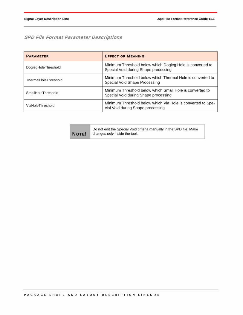
SPD File Format Parameter Descriptions
PARAMETER EFFECT OR MEANING
DoglegHoleThreshold Minimum Threshold below which Dogleg Hole is converted to Special Void during Shape processing
ThermalHoleThreshold Minimum Threshold below which Thermal Hole is converted to Special Void Shape Processing
SmallHoleThreshold Minimum Threshold below which Small Hole is converted to Special Void during Shape processing
ViaHoleThreshold Minimum Threshold below which Via Hole is converted to Spe-cial Void during Shape processing
NOTE!Do not edit the Special Void criteria manually in the SPD file. Make changes only inside the tool.

P A C K A G E S H A P E A N D L A Y O U T D E S C R I P T I O N L I N E S 2 5
Signal Layer Description Line .spd File Format Reference Guide 11.1
Medium Description LineSpeed2000 emulates the effects of mesh planes by adjusting the capacitance, inductance, admittance and resistance parameters in the field solver module.
Required entries for optional statement parameters must be introduced manually to the text file using a text editor. Enter additional information in all three description lines (Patch, Medium and Signal).
General FormMediumXXXX thickness = f1 [Permittivity = f2] [LossTangent = f3] [Material = s1]
+ [Conductivity = f4] [File = s1 Model = s2]
+ [ AreaAdj=< ( [ X0 = f5 Y0 = f6 Xw = f7 Yw = f8 ]
+ [ Cr = f9 ] [ Gr = f10 ] [ Lxr = f11 ] [ Lyr = f12 ] ) ,
+ ( [ X0 = f13 Y0 = f14 Xw = f15 Yw = f16 ]
+ [ Cr = f17 ] [ Gr = f18 ] [ Lxr = f19 ] [ Lyr = f20 ] ) ,
+ … > ]
X+
X-
X+Z
Y+
Y+
Y-
(X0, Y0)(f5, f6)
(0,0)
overlap
Xwf7
package origin
Ywf8
(X0, Y0)(f13, f14)
15f15XwXwXw
f16YYw

P A C K A G E S H A P E A N D L A Y O U T D E S C R I P T I O N L I N E S 2 6
Signal Layer Description Line .spd File Format Reference Guide 11.1
Medium Example 1Medium$5 Thickness = 1.270000e+002u Permittivity = 4.000000e+000
+ Conductivity = 1.000000e-002
Medium Example 2Medium04 Thickness = 5.000000e+002u Permittivity = 4.000000e+000
+ LossTangent = 0.000000e+000
+ AreaAdj=<
+ (X0 = 0 Y0 = 1 Xw = 3 Yw = 2
+ Cr = 0.5 Gr = 0.2 Lxr = 0.4 Lyr =0.8) ,
+ (X0 = -1 Y0 = -2 Xw = 4 Yw = 1
+ Cr = 0.6 Gr = 0.1 Lxr = 0.8 Lyr =0.7)
+ >
Medium Example 3Medium03 Thickness = 5.000000e+002u Material = FR4
+ LossTangent = 0.000000e+000
Medium Parameter Descriptions
PARAMETER EFFECT OR MEANING
Mediumxxxx Name of the dielectric medium, where xxxx can be any characters
Thickness = f1 Thickness of dielectric medium
Permittivity = f2
Relative permittivity of the dielectric medium
If a data file is provided for the dielectric medium (see File parameter below), the loss tangent of the dielectric medium will be determined by the data file and val-ues in the entries of LossTangent and Conductivity will be overwritten.
LossTangent = f3 Loss tangent of the dielectric medium. Default is 0.
Conductivity = f4 Conductivity of the dielectric medium. Default = 10-50 S/m
Material = f3 Material of medium
If Loss Tangent and Conductivity are both given, the loss of the dielectric medium is determined by the Loss Tangent.
File = s1 Character string for the name of the data file that stores the dielectric model.
Model = s2 Character string for the name of the model in the data file s1

P A C K A G E S H A P E A N D L A Y O U T D E S C R I P T I O N L I N E S 2 7
Signal Layer Description Line .spd File Format Reference Guide 11.1
AreaAdj = < ( …), (…), …>
Keyword of the capacitance, inductance and admittance adjustment option. Both “< >” pair and “( )” pairs are required delimiters in the “AreaAdj” option.
Symbol “<” indicates the start of an AreaAdj option, and symbol “>” indicates the end of the option. An AreaAdj option may contain more than one adjustment items.
Data enclosed in each parenthesis “( )” pair denote the content of one adjustment item.
In each adjustment item, either all or none of X0, Y0, Xw and Yw parameters should exist. If none of the X0, Y0, Xw and Yw parameters is specified, the adjust-ment range is the whole layer.
The order of the adjustment items in AreaAdj option is meaningful in the case of overlap.
If the adjustment areas (determined by X0, Y0, Xw and Yw parameters) in two adjustment items overlap, the latter one of the two adjustment items is taken as the base to adjust capacitance, inductance and admittance within the overlapping area in the medium layer.
X0 = f5, f13, … X coordinates of the lower left corner of the rectangular adjustment area.
Y0 = f6, f14, … Y coordinates of the lower left corner of the rectangular adjustment area.
Xw = f7, f15, … Lengths of the rectangular adjustment area along the horizontal x direction. Must be a positive number.
Yw = f8, f16, … Lengths of the rectangular adjustment area along the vertical y direction. Must be a positive number.
Cr = f9, f17, … Adjustment ratios of the distributed capacitance C. Must be a positive number. Default value: 1.0.
Gr = f10, f18, … Adjustment ratios of the distributed admittance G. Must be a positive number. Default value: 1.0.
Lxr = f11, f19, … Adjustment ratios of the distributed inductance Lx in x direction. Must be a posi-tive number. Default value: 1.0.
Lyr = f12, f20, … Adjustment ratios of the distributed inductance Ly in y direction. Must be a posi-tive number. Default value: 1.0.
PARAMETER EFFECT OR MEANING

P A C K A G E S H A P E A N D L A Y O U T D E S C R I P T I O N L I N E S 2 8
Signal Layer Description Line .spd File Format Reference Guide 11.1
Patch Description LineSpeed2000 emulates the effects of mesh planes by adjusting the capacitance, inductance, admittance and resistance parameters in the field solver module.
Required entries for optional statement parameters must be introduced manually to the text file using a text editor. Enter the additional information in all three description lines (patch, medium, and signal).
For detailed information refer to Medium Description Line.
General FormPatchxxxx [Thickness = f1] [Conductivity = f2] Shape = s1 Layer = s2
+ [ AreaAdj=< ( [ X0 = f3 Y0 = f4 Xw = f5 Yw = f6 ]
+ [ Rxr = f7 ] [ Ryr = f8 ] ) ,
+ ( [ X0 = f9 Y0 = f10 Xw = f11 Yw = f12 ] [ Rxr = f13 ] [ Ryr = f14 ] ) ,
+ … > ]
Patch Example 1Patch$GND Thickness = 3.048000e+001u Conductivity = 5.959000e+007
+ Shape = Shape$GND
Patch Example 2Patch01 Thickness = 3.560000e+001u Conductivity = 5.800000e+007
+ Shape = Shape001
+ Layer = Signal01
+ AreaAdj=<
+ (X0 = 0 Y0 = 1 Xw = 3 Yw = 2
+ Rxr = 1.0 Ryr =4.0) ,
+ (X0 = -1 Y0 = -2 Xw = 4 Yw = 1
+ Rxr = 2.0 Ryr =3.0)
+ >
X+
X-
X+Z
Y+
Y+
Y-
(X0, Y0)(f3, f4)
(0,0)
overlap
Xwf5
package origin
Ywf6
(X0, Y0)(f9, f10)
11f11XwXwXw
f12YYw

P A C K A G E S H A P E A N D L A Y O U T D E S C R I P T I O N L I N E S 2 9
Signal Layer Description Line .spd File Format Reference Guide 11.1
Patch Parameter Descriptions
PARAMETER EFFECT OR MEANING
Patchxxxx Name of the patch, where xxxx can be any characters.
Thickness = f1 Metal patch thickness. Default: Thickness of the signal layer where patch is located.
Conductivity = f2 Conductivity of the metal patch. Default value: 5.8e7 S/m.
Shape = s1 Name of the Shape specified in the shape description lines.
Layer = s2 Signal layer name for the metal patch.
AreaAdj = < ( …), (…), …>
Keyword of resistance adjustment option. Both < > and ( ) pairs are required delimit-ers in the AreaAdj option.
Symbol < indicates start of an AreaAdj option. Symbol > indicates end of the option. Data enclosed in parenthesis ( ) pair denotes content of one adjustment item.
An AreaAdj option may contain more than one adjustment item. In each adjustment item, either all or none of X0, Y0, Xw and Yw parameters should exist.
If none of the X0, Y0, Xw and Yw parameters is specified, adjustment range is the whole layer.
Order of adjustment items in AreaAdj option is meaningful in case of overlap.
If adjustment areas (determined by X0, Y0, Xw and Yw parameters) in two adjust-ment items overlap, the latter one of the two adjustment items is taken as the base to adjust resistance within the overlapping area in the plane or patch layer.
X0 = f3, f9, … x coordinate of the lower left corner of the rectangular adjustment area.
Y0 = f4, f10, … y coordinate of the lower left corner of the rectangular adjustment area.
Xw = f5, f11, … Length of the rectangular adjustment area along the horizontal x direction. Must be a positive number.
Yw = f6, f12, … Length of the rectangular adjustment area along the vertical y direction. Must be a positive number.
Rxr = f7, f13, … Adjustment ratio of the distributed resistance Rx in x direction. Must be a positive number. Default value: 1.0.
Ryr = f8, f14, … Adjustment ratio of the distributed resistance Ry in y direction. Must be a positive number. Default value: 1.0.
P A C K A G E S H A P E A N D L A Y O U T D E S C R I P T I O N L I N E S 3 0
Trace Surface Roughness Description Lines .spd File Format Reference Guide 11.1
TRACE SURFACE ROUGHNESS DESCRIPTION LINESEach Trace surface roughness description line stores the root mean square deviation of stores Trace thickness for Traces on associated layers.
General Format[{.TraceSurfaceRoughness [Layer = layer] Roughness = rms}]
Trace Surface Roughness Parameter Descriptions
PADSTACK DESCRIPTION LINEThe Padstack information is used to translate the pad geometry information.
Each Padstack stores the pad geometry for associated layers.
General Format.PadStackDef PadStackName [OuterRadius] [InnerRadius] [Material = material name][Conductivity = conductivity value]
.PadDef LayerName
[Regular { Circle r | Box w h | Square a | RoundedRect_X w h | Rounded Rect_Y w h |Polygon {x, y} } offSetX = <xOff> offSetY = <yOff> ]
[Anti { Circle r | Box w h | Square a | RoundedRect_X w h | Rounded Rect_Y w h | Poly-gon {x, y} } offSetX = <xOff> offSetY = <yOff> ]
[Thermal { Circle r | Box w h | Square a | RoundedRect_X w h | Rounded Rect_Y w h |Polygon {x, y} } offSetX = <xOff> offSetY = <yOff> ]
.EndPadDef
...
.EndPadStackDef
PARAMETER EFFECT OR MEANING
Layer
If Layer is not present, the roughness is defined for Traces on all layers. This is the global roughness.
If Layer is present, the roughness is defined for traces on that layer. This is the local roughness. Local roughness overrides global roughness.
RoughnessThe root mean square deviation of Trace thickness and is in length unit. Layer is a layer name. Default: 0, means smooth surface.
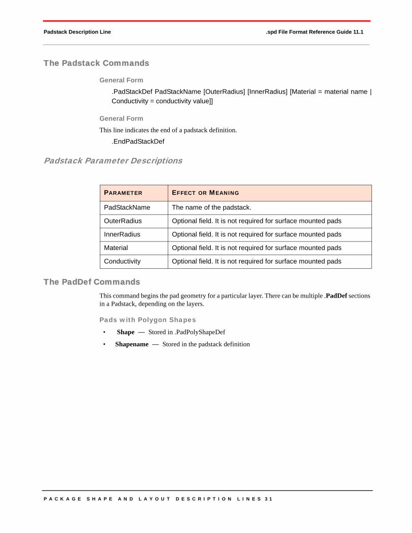
P A C K A G E S H A P E A N D L A Y O U T D E S C R I P T I O N L I N E S 3 1
Padstack Description Line .spd File Format Reference Guide 11.1
The Padstack Commands
General Form.PadStackDef PadStackName [OuterRadius] [InnerRadius] [Material = material name |Conductivity = conductivity value]]
General FormThis line indicates the end of a padstack definition.
.EndPadStackDef
Padstack Parameter Descriptions
The PadDef CommandsThis command begins the pad geometry for a particular layer. There can be multiple .PadDef sections in a Padstack, depending on the layers.
Pads with Polygon Shapes
• Shape — Stored in .PadPolyShapeDef
• Shapename — Stored in the padstack definition
PARAMETER EFFECT OR MEANING
PadStackName The name of the padstack.
OuterRadius Optional field. It is not required for surface mounted pads
InnerRadius Optional field. It is not required for surface mounted pads
Material Optional field. It is not required for surface mounted pads
Conductivity Optional field. It is not required for surface mounted pads
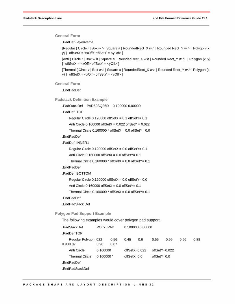
P A C K A G E S H A P E A N D L A Y O U T D E S C R I P T I O N L I N E S 3 2
Padstack Description Line .spd File Format Reference Guide 11.1
General Form.PadDef LayerName
[Regular { Circle r | Box w h | Square a | RoundedRect_X w h | Rounded Rect_Y w h | Polygon {x,y} } offSetX = <xOff> offSetY = <yOff> ]
[Anti { Circle r | Box w h | Square a | RoundedRect_X w h | Rounded Rect_Y w h | Polygon {x, y}} offSetX = <xOff> offSetY = <yOff> ]
[Thermal { Circle r | Box w h | Square a | RoundedRect_X w h | Rounded Rect_Y w h | Polygon {x,y} } offSetX = <xOff> offSetY = <yOff> ]
General Form.EndPadDef
Padstack Definition Example.PadStackDef PAD60SQ36D 0.100000 0.00000
.PadDef TOP
Regular Circle 0.120000 offSetX = 0.1 offSetY= 0.1
Anti Circle 0.160000 offSetX = 0.022 offSetY = 0.022
Thermal Circle 0.160000 * offSetX = 0.0 offSetY= 0.0
.EndPadDef
.PadDef INNER1
Regular Circle 0.120000 offSetX = 0.0 offSetY= 0.1
Anti Circle 0.160000 offSetX = 0.0 offSetY= 0.1
Thermal Circle 0.160000 * offSetX = 0.0 offSetY= 0.1
.EndPadDef
.PadDef BOTTOM
Regular Circle 0.120000 offSetX = 0.0 offSetY= 0.0
Anti Circle 0.160000 offSetX = 0.0 offSetY= 0.1
Thermal Circle 0.160000 * offSetX = 0.0 offSetY= 0.1
.EndPadDef
.EndPadStack Def
Polygon Pad Support ExampleThe following examples would cover polygon pad support.
.PadStackDef POLY_PAD 0.100000 0.00000
.PadDef TOP
Regular Polygon .022 0.56 0.45 0.6 0.55 0.99 0.66 0.880.900.87 0.98 0.87
Anti Circle 0.160000 offSetX=0.022 offSetY=0.022
Thermal Circle 0.160000 * offSetX=0.0 offSetY=0.0
.EndPadDef
.EndPadStackDef
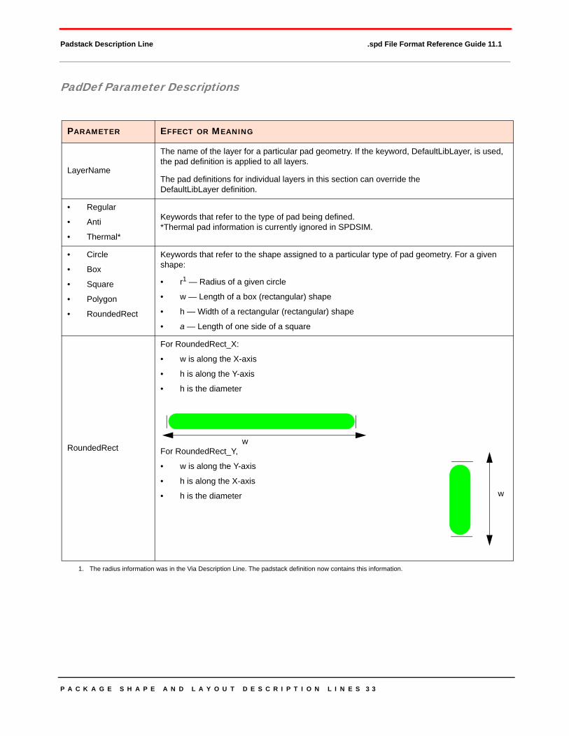
P A C K A G E S H A P E A N D L A Y O U T D E S C R I P T I O N L I N E S 3 3
Padstack Description Line .spd File Format Reference Guide 11.1
PadDef Parameter Descriptions
PARAMETER EFFECT OR MEANING
LayerName
The name of the layer for a particular pad geometry. If the keyword, DefaultLibLayer, is used, the pad definition is applied to all layers.
The pad definitions for individual layers in this section can override the DefaultLibLayer definition.
• Regular
• Anti
• Thermal*
Keywords that refer to the type of pad being defined.*Thermal pad information is currently ignored in SPDSIM.
• Circle
• Box
• Square
• Polygon
• RoundedRect
Keywords that refer to the shape assigned to a particular type of pad geometry. For a given shape:
• r1 — Radius of a given circle
• w — Length of a box (rectangular) shape
• h — Width of a rectangular (rectangular) shape
• a — Length of one side of a square
RoundedRect
For RoundedRect_X:
• w is along the X-axis
• h is along the Y-axis
• h is the diameter
For RoundedRect_Y,
• w is along the Y-axis
• h is along the X-axis
• h is the diameter
1. The radius information was in the Via Description Line. The padstack definition now contains this information.
w
w

P A C K A G E S H A P E A N D L A Y O U T D E S C R I P T I O N L I N E S 3 4
Material Description Lines .spd File Format Reference Guide 11.1
MATERIAL DESCRIPTION LINESMaterial description lines specify information of material models.
The Material description lines section begins with the command .Material and ends with the com-mand .EndMaterial.
Specify Material ModelYou can specify the following material model:
• .DielectricModel• .MetalModel• .ThermalModel
The model description ends with:
• .EndDielectricModel• .EndMetalModel• .EndThermalModel
General Form.Material
.MetalModel ModelName
*CommentLine
TemperatureValue ConductivityValue
.EndMetalModel
.DielectricModel ModeName
*CommentLine
FrequencyValue PermittivityValue LossTangentValue
.EndDielectricModel
.ThermalModel ModelName
*CommentLine
TemperatureValueConductivityValue DensityValue HeatcapacityValue
.EndThermalModel
.EndMaterial

P A C K A G E S H A P E A N D L A Y O U T D E S C R I P T I O N L I N E S 3 5
Material Description Lines .spd File Format Reference Guide 11.1
Material Section Command Example.Material
.MetalModel silver
*Temperature(C) Conductivity(S/m)
2.0000000e+001 6.301000e+007
.EndMetalModel
.DielectricModel FR4_4.2
*Frequency(MHz) Permittivity LossTangent
1.000000e+002 4.200000e+000 2.300000e-002
.EndDielectricModel
.ThermalModel silver
*Temperature(C) Conductivity(W/(m.K)) Density(kg/m3) Heatcapacity(J/(kg.K))
2.700000e+001 4.290000e+002 1.050000e+004 2.320000e+002
.EndThermalModel
.EndMaterial
Material Model Parameter Descriptions
PARAMETER EFFECT OR MEANING
.Material Keyword for beginning of material models section line
.EndMaterial Keyword for end of material models section line
ModelName A character string for the name of the material model
TemperatureValue Value of Temperature
ConductivityValue Value of Conductivity
FrequencyValue Value of Frequency
PermittivityValue Value of Permittivity
LossTangentValue Value of Loss Tangent
DensityValue Value of Density
HeatcapacityValue Value of Heat Capacity

P A C K A G E S H A P E A N D L A Y O U T D E S C R I P T I O N L I N E S 3 6
Node Description Line .spd File Format Reference Guide 11.1
NODE DESCRIPTION LINE
General FormNode[Affix]xxx[!!PinName][::NetName]
[PolygonVertex]
x = f1
y = f2
Layer = s1
[Contact = n1]
[Padstack = PadStackName]
[AbsoluteRotation = Angle]
Node ExampleNode8Zgx4080!!U27-1::VSS X = -2.200912e+001mm Y = -2.000912e+001mm
+ Layer = Signal_Ground Contact = 1
Node Padstack Information ExampleNode9321!!1::R_BNC_5P X = 1.194100e+001mm Y = 2.009700e+001mm Layer = Sig-nal$L1_TOPSIDE Contact = 1 PadStack = PAD88CIR78D AbsoluteRotation = 180
NOTE!A Node can only be on a Plane or a Signal layer. If the Node is an end Node of a Trace, electric contact with the Trace is assumed, and the Contact option does not need to be specified.
If a Node is an upper or lower end of a Via located on a plane or patch, two possibilities exist: (1) the Node is in contact with the metal or (2) the Node is NOT in contact with the metal.
x+
x-
X+Z
Y+
y+
y-
(x,y)
(0,0)package origin
node

P A C K A G E S H A P E A N D L A Y O U T D E S C R I P T I O N L I N E S 3 7
Node Description Line .spd File Format Reference Guide 11.1
Node Parameter Descriptions
PARAMETER EFFECT OR MEANING
Node Node keyword
Affix Optional 1 to 4 characters
xxx A character string for the name of the Node
!!PinName Optional name associated with the pin
::NetName Optional Net name associated with the object
PolygonVertex If PolygonVertex is present, the node coincides with a polygon vertex. The Trace, of which the Node is a terminal, connects to a metal patch.
x =f1 X coordinate of the Node with respect to the package origin
y = f2 Y coordinate of the Node with respect to the package origin
Layer =s1 Name of the Plane or Signal layer on which the Node resides
Contact
= 1 The Node has electric contact with the metal shape or patch. Default
= 0 The Node has no electric contact with the metal Shape (or Patch)
[Padstack = PadStackName] The name of the Padstack. Optional
[AbsoluteRotation = Angle] The angle of absolute rotation in degrees. Optional

P A C K A G E S H A P E A N D L A Y O U T D E S C R I P T I O N L I N E S 3 8
Via Description Line .spd File Format Reference Guide 11.1
VIA DESCRIPTION LINE
General FormVia[Affix]xxx[::NetName]
UpperNode = s1
LowerNode = s2
+ [Conductivity = f1]
[Color = s4]
[Padstack = PadStackName]
[AbsoluteRotation = Angle]
Via ExampleVia8Zgx0100::GND UpperNode = Node04227 LowerNode = Node3373 Radius = R0
+ Conductivity = 5.80e+007 Color = red
Via Padstack Information ExampleVia1:GND UpperNode = Node13815::GND LowerNode = Node13816::GND Color = yellow Pad-Stack = PAD60SQ36D AbsoluteRotation = 270
NOTE! Radius information is stored in Padstack.
Parameter [radius = value] is not valid.
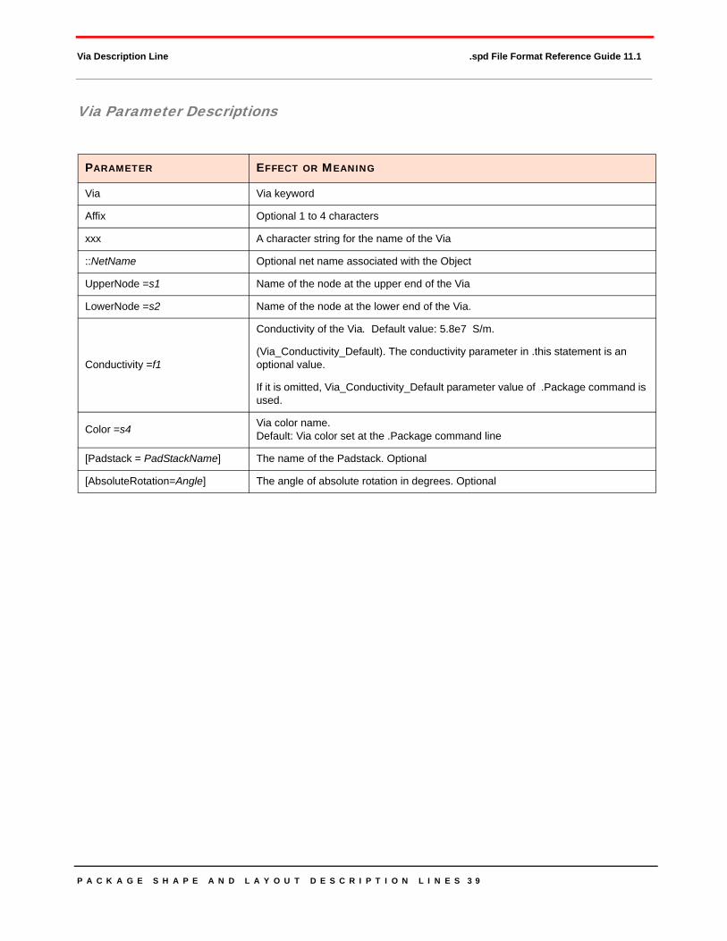
P A C K A G E S H A P E A N D L A Y O U T D E S C R I P T I O N L I N E S 3 9
Via Description Line .spd File Format Reference Guide 11.1
Via Parameter Descriptions
PARAMETER EFFECT OR MEANING
Via Via keyword
Affix Optional 1 to 4 characters
xxx A character string for the name of the Via
::NetName Optional net name associated with the Object
UpperNode =s1 Name of the node at the upper end of the Via
LowerNode =s2 Name of the node at the lower end of the Via.
Conductivity =f1
Conductivity of the Via. Default value: 5.8e7 S/m.
(Via_Conductivity_Default). The conductivity parameter in .this statement is an optional value.
If it is omitted, Via_Conductivity_Default parameter value of .Package command is used.
Color =s4 Via color name. Default: Via color set at the .Package command line
[Padstack = PadStackName] The name of the Padstack. Optional
[AbsoluteRotation=Angle] The angle of absolute rotation in degrees. Optional
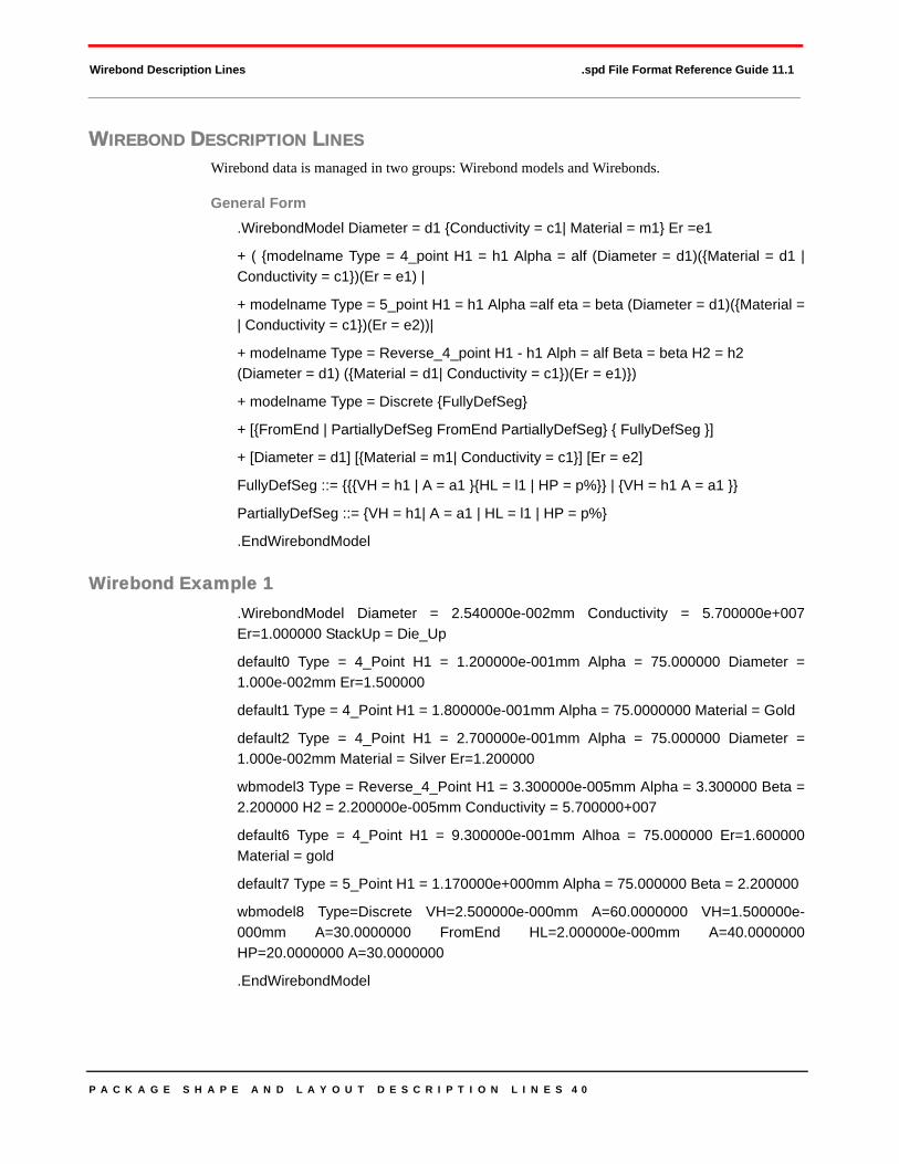
P A C K A G E S H A P E A N D L A Y O U T D E S C R I P T I O N L I N E S 4 0
Wirebond Description Lines .spd File Format Reference Guide 11.1
WIREBOND DESCRIPTION LINESWirebond data is managed in two groups: Wirebond models and Wirebonds.
General Form.WirebondModel Diameter = d1 {Conductivity = c1| Material = m1} Er =e1
+ ( {modelname Type = 4_point H1 = h1 Alpha = alf (Diameter = d1)({Material = d1 |Conductivity = c1})(Er = e1) |
+ modelname Type = 5_point H1 = h1 Alpha =alf eta = beta (Diameter = d1)({Material =| Conductivity = c1})(Er = e2))|
+ modelname Type = Reverse_4_point H1 - h1 Alph = alf Beta = beta H2 = h2 (Diameter = d1) ({Material = d1| Conductivity = c1})(Er = e1)})
+ modelname Type = Discrete {FullyDefSeg}
+ [{FromEnd | PartiallyDefSeg FromEnd PartiallyDefSeg} { FullyDefSeg }]
+ [Diameter = d1] [{Material = m1| Conductivity = c1}] [Er = e2]
FullyDefSeg ::= {{{VH = h1 | A = a1 }{HL = l1 | HP = p%}} | {VH = h1 A = a1 }}
PartiallyDefSeg ::= {VH = h1| A = a1 | HL = l1 | HP = p%}
.EndWirebondModel
Wirebond Example 1.WirebondModel Diameter = 2.540000e-002mm Conductivity = 5.700000e+007Er=1.000000 StackUp = Die_Up
default0 Type = 4_Point H1 = 1.200000e-001mm Alpha = 75.000000 Diameter =1.000e-002mm Er=1.500000
default1 Type = 4_Point H1 = 1.800000e-001mm Alpha = 75.0000000 Material = Gold
default2 Type = 4_Point H1 = 2.700000e-001mm Alpha = 75.000000 Diameter =1.000e-002mm Material = Silver Er=1.200000
wbmodel3 Type = Reverse_4_Point H1 = 3.300000e-005mm Alpha = 3.300000 Beta =2.200000 H2 = 2.200000e-005mm Conductivity = 5.700000+007
default6 Type = 4_Point H1 = 9.300000e-001mm Alhoa = 75.000000 Er=1.600000Material = gold
default7 Type = 5_Point H1 = 1.170000e+000mm Alpha = 75.000000 Beta = 2.200000
wbmodel8 Type=Discrete VH=2.500000e-000mm A=60.0000000 VH=1.500000e-000mm A=30.0000000 FromEnd HL=2.000000e-000mm A=40.0000000HP=20.0000000 A=30.0000000
.EndWirebondModel

P A C K A G E S H A P E A N D L A Y O U T D E S C R I P T I O N L I N E S 4 1
Wirebond Description Lines .spd File Format Reference Guide 11.1
Wirebond Example 2WirebondModel Diameter = 2.540000e-002mm Material = copper Er = 1.000 StackUp =Die_Up
Wirebond Parameter Descriptions
PARAMETER EFFECT OR MEANING
WirebondModel Keyword
Diameter = s1 Diameter of the Wirebond model
Conductivity = c1 Conductivity of the Wirebond model
Material = m1 Material of Wirebond model
Er = e1 Relative permittivity of the Wirebond model
modelname Type
Choose from:• 4_point• 5_point• Reverse_4_point• .KNS Standard• .KNS Loop• Discrete
H1 = h1 Height of the Wirebond starting from the die
Alpha = alf Angle between H1 and the length of the Wirebond
Beta = beta Angle between H2 and the length of the Wirebond
H2 = h2 Height of the Wirebond starting from the Via
Span = s1 Horizontal section length in the K&S loop model as a fraction of separation between start-ing and ending Node locations
Diameter = d1 Diameter of the Trace, which becomes the diameter of the Wirebond
Material = m1 If selecting a data file, use a meta type to calculate the conductivity of the model
Direction = d1 Whether the Wirebond is above (Die-Up) or below (Die_Down) the die
Flip Starts the model description at the Wirebond starting Node (NO) or ending Node (YES)
conductivity Conductivity of the given Wirebond
Er Use the common value if set to empty. Relative permittivity of the Wirebond
VH Vertical height of Wirebond segment in Discrete model description
HL Horizontal length of Wirebond segment in Discrete model description
HP Horizontal percent of Wirebond segment to total distance of starting and ending Nodes in Discrete model description
A Angle of Wirebond segment to horizontal axis in Discrete model description
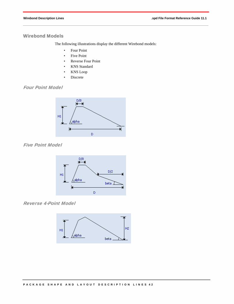
P A C K A G E S H A P E A N D L A Y O U T D E S C R I P T I O N L I N E S 4 2
Wirebond Description Lines .spd File Format Reference Guide 11.1
Wirebond ModelsThe following illustrations display the different Wirebond models:
• Four Point• Five Point• Reverse Four Point• KNS Standard• KNS Loop• Discrete
Four Point Model
Five Point Model
Reverse 4-Point Model

P A C K A G E S H A P E A N D L A Y O U T D E S C R I P T I O N L I N E S 4 3
Wirebond Description Lines .spd File Format Reference Guide 11.1
The K&S Standard Model
The K&S Loop Model
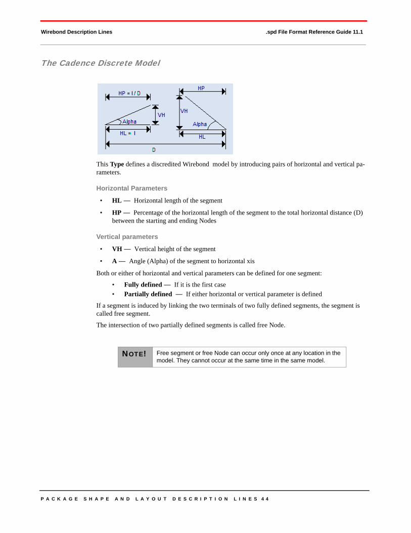
P A C K A G E S H A P E A N D L A Y O U T D E S C R I P T I O N L I N E S 4 4
Wirebond Description Lines .spd File Format Reference Guide 11.1
The Cadence Discrete Model
This Type defines a discredited Wirebond model by introducing pairs of horizontal and vertical pa-rameters.
Horizontal Parameters
• HL — Horizontal length of the segment
• HP — Percentage of the horizontal length of the segment to the total horizontal distance (D) between the starting and ending Nodes
Vertical parameters
• VH — Vertical height of the segment
• A — Angle (Alpha) of the segment to horizontal xis
Both or either of horizontal and vertical parameters can be defined for one segment:
• Fully defined — If it is the first case• Partially defined — If either horizontal or vertical parameter is defined
If a segment is induced by linking the two terminals of two fully defined segments, the segment is called free segment.
The intersection of two partially defined segments is called free Node.
NOTE! Free segment or free Node can occur only once at any location in the model. They cannot occur at the same time in the same model.
P A C K A G E S H A P E A N D L A Y O U T D E S C R I P T I O N L I N E S 4 5
WirebondGroup Description Lines .spd File Format Reference Guide 11.1
WIREBONDGROUP DESCRIPTION LINES
General Form for WirebondGroup(.WirebondGroup DieName [Ref = Wirebond Reference Layer Name]
+ (Wirebond[Affix]xxx[::Netname] StartingNode=n1 EndingNode=n2
+ Model=m [Color=c])
.EndWirebondGroup)
WireBondGroup Example.WirebondGroup Test_17 Ref = Signal$01
Wirebond01 StartingNode = Node021 EndingNode = Node022 Model=WBModel1
Wirebond02 StartingNode = Node023 EndingNode = Node024 Model=WBModel1
Wirebond03 StartingNode = Node025 EndingNode = Node026 Model=WBModel1
Wirebond04 StartingNode = Node027 EndingNode = Node028 Model=WBModel1
.EndWirebondGroup
WirebondGroup Parameter Descriptions
PARAMETER EFFECT OR MEANING
WirebondGroup Key word
DieName Name of the die that the Wirebond group belongs
Ref = Wirebond Reference Layer Name The reference layer, which is calculated
Affix Optional 1 to 4 characters
xxx A character string for the name of the Trace
::NetName Optional Net name associated with the Object
StartingNode = n1 Name of the Node at one end of the Wirebond
EndingNode = n2 Name of the Node at the other end of the Wirebond
Model = m The model name
Color =s3 Wirebond color name Default: Trace color set at Signal layer description line
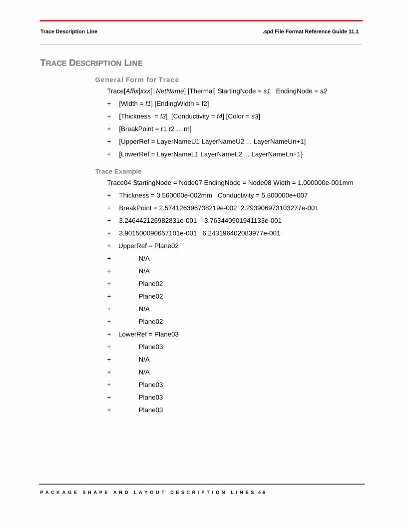
P A C K A G E S H A P E A N D L A Y O U T D E S C R I P T I O N L I N E S 4 6
Trace Description Line .spd File Format Reference Guide 11.1
TRACE DESCRIPTION LINE
General Form for TraceTrace[Affix]xxx[::NetName] [Thermal] StartingNode = s1 EndingNode = s2
+ [Width = f1] [EndingWidth = f2]
+ [Thickness = f3] [Conductivity = f4] [Color = s3]
+ [BreakPoint = r1 r2 ... rn]
+ [UpperRef = LayerNameU1 LayerNameU2 ... LayerNameUn+1]
+ [LowerRef = LayerNameL1 LayerNameL2 ... LayerNameLn+1}
Trace ExampleTrace04 StartingNode = Node07 EndingNode = Node08 Width = 1.000000e-001mm
+ Thickness = 3.560000e-002mm Conductivity = 5.800000e+007
+ BreakPoint = 2.574126396738219e-002 2.293906973103277e-001
+ 3.246442126982831e-001 3.763440901941133e-001
+ 3.901500090657101e-001 6.243196402083977e-001
+ UpperRef = Plane02
+ N/A
+ N/A
+ Plane02
+ Plane02
+ N/A
+ Plane02
+ LowerRef = Plane03
+ Plane03
+ N/A
+ N/A
+ Plane03
+ Plane03
+ Plane03

P A C K A G E S H A P E A N D L A Y O U T D E S C R I P T I O N L I N E S 4 7
Trace Description Line .spd File Format Reference Guide 11.1
Trace Parameter Descriptions
PARAMETER EFFECT OR MEANING
Trace Trace keyword
Affix Optional 1 to 4 characters
xxx A character string for the name of the Trace
::NetName Optional Net name associated with the Object
Thermal
If the Thermal keyword is present, the Trace is a thermal Trace, and the Break-Point, UpperRef, and LowerRef sections will not exist in the statement
If the Thermal keyword is absent, the BreakPoint, UpperRef, and LowerRef sec-tions exist in the statement
StartingNode =s1 Name of the Node at one end of the Trace
EndingNode =s2 Name of the Node at the other end of the Trace
Thickness = f1 Thickness of the Trace Default: Thickness defined in Signal layer description
Width = f2 Width of the Trace. Default: Width defined in Signal layer description line
If EndingWidth is specified, this field is the width of the Trace at the starting Node
EndingWidth = f3 Width of the Trace at the ending Node. If the values of Width and EndingWidth aren’t equal, the Trace is called a Tapered Trace; otherwise, Uniform Trace
Conductivity =f4 Conductivity of the Trace conductor Default: Conductivity defined in Signal layer description line
Color =s3 Trace color name Default: Trace color set at Signal layer description line
BreakPoint = r1 r2 ... rn ri is the ratio (0 ~ 1) of the distance from the starting Node to the ith-breakpoint over the whole length of the Trace
UpperRef Name of the upper reference plane for the Trace section
LowerRef Name of the lower reference plane for the Trace section

P A C K A G E S H A P E A N D L A Y O U T D E S C R I P T I O N L I N E S 4 8
ClippedTrace Line .spd File Format Reference Guide 11.1
CLIPPEDTRACE LINEThe Trace clipping procedure in the program adds following line in the .spd file after the Via and Trace section.
General FormClippedTrace = s1
ClippedTrace ExampleWhere s1 is information used internally by executable modules and it should not bemodified by the user.
ClippedTrace = 540A09FF-6FF475BF-4F822248-956A6934
SEGMENTED TRACE LINEThe Trace over split plane algorithm in the program adds the following line in the .spd file after the Via and Trace section.
General FormSegmentedTrace = s1
where s1 is information used internally by executable modules and it should not bemodified by the user.
SegmentedTrace ExampleSegmentedTrace = 540A09FF-6FF475BF-4F822248-956A6934
CPL DESCRIPTION LINEUse this line for a coupled line object consisting of single Trace segments.
This description is deprecated in favor of the GCPL description discussed in GCPL Description Block.
General FormCPLxxxx Trace1 Trace2 … TraceN
CPL Parameter Descriptions
PARAMETER EFFECT OR MEANING
CPLxxxx Name of the coupled Trace object, where xxxx can be any characters
Trace1 Trace2 … TraceN List of Trace names
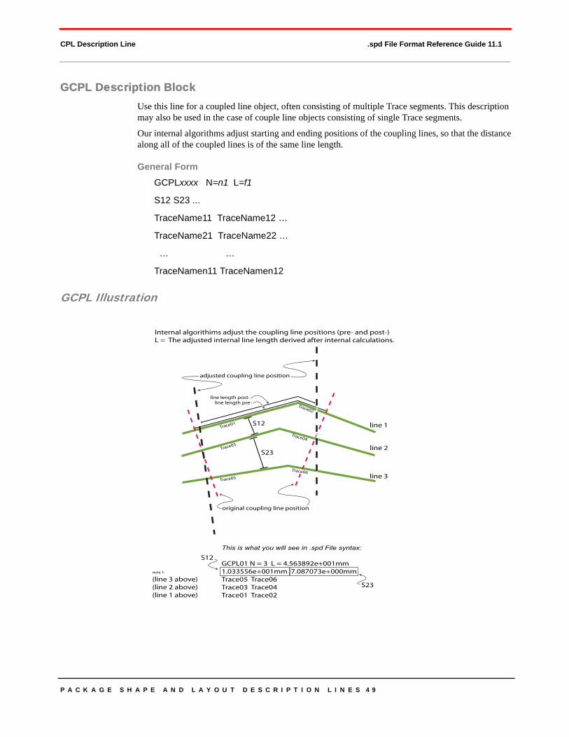
P A C K A G E S H A P E A N D L A Y O U T D E S C R I P T I O N L I N E S 4 9
CPL Description Line .spd File Format Reference Guide 11.1
GCPL Description BlockUse this line for a coupled line object, often consisting of multiple Trace segments. This description may also be used in the case of couple line objects consisting of single Trace segments.
Our internal algorithms adjust starting and ending positions of the coupling lines, so that the distance along all of the coupled lines is of the same line length.
General FormGCPLxxxx N=n1 L=f1
S12 S23 ...
TraceName11 TraceName12 …
TraceName21 TraceName22 …
… …
TraceNamen11 TraceNamen12
GCPL Illustration
line 1Trace01
Trace02
Trace03
Trace04
Trace05
line 2
S12
S12
line 3
original coupling line position
line length pre-line length post-
adjusted coupling line position
Trace06
note 1:
(line 3 above)(line 2 above)(line 1 above)
This is what you will see in .spd File syntax:
GCPL01 N = 3 L = 4.563892e+001mm1.033556e+001mm 7.087073e+000mm Trace05 Trace06 Trace03 Trace04 Trace01 Trace02
Internal algorithims adjust the coupling line positions (pre- and post-)L = The adjusted internal line length derived after internal calculations.
S23
S23

P A C K A G E S H A P E A N D L A Y O U T D E S C R I P T I O N L I N E S 5 0
Lead Description Lines .spd File Format Reference Guide 11.1
GCPL Parameter Descriptions
LEAD DESCRIPTION LINESLead is a structure. Lead data is managed in two groups.
• Lead Instances• Lead Models
General Form for LeadModel.LeadModel {Conductivity = c1| Material = m1} Er = e1
{ {modelname Type = LeadType_1 Thickness = t Width = w L_up=l_1 L_low=l_2 ({Con-ductivity = c1| Material = m1})(Er = e1)|
modelname Type = LeadType_2 Thickness = t Width = w Ratio_up=r1 Ratio_low=r2({Conductivity = c1 | Material = m1})(Er = e1)|
modelname Type = LeadType_3 Thickness = t WWidth=wu NWidth=wl NarrowRatio=r0
+ L_up=l_1 L_low=l_2 R_up=Ru R_low=Rl ({Conductivity = c1| Material =m1})(Er = e1)|
modelname Type = LeadType_4 Thickness = t WWidth=wu NWidth=wl NarrowRatio=r0
+ Ratio_up=r1 Ratio_low=r2 R_up=Ru R_low=Rl ({Conductivity = c1| Material = m1})(Er= e1)} }
.EndLeadModel
PARAMETER EFFECT OR MEANING
GCPLxxxx Name of the coupled line object, where xxxx can be any characters
N=n1 Number of coupled lines
L=f 1 Length of the coupled lines. The length of the couple lines is computed by an inter-nal algorithm at the time the coupled lines are set up.
S12 S23Separations between n1 coupled lines. First number is the separation between line 1 and 2. Second number is the separation between line 2 and 3, etc. The separation between two lines is the average separation computed by an internal algorithm.
TraceName11 TraceName12
List of Trace names for line 1. Note the lines are recorded in the .spd file from bot-tom coupled line to top coupled line.
TraceName21 TraceName22 List of Trace names for line 2

P A C K A G E S H A P E A N D L A Y O U T D E S C R I P T I O N L I N E S 5 1
Lead Description Lines .spd File Format Reference Guide 11.1
Lead Model Example* Lead Model Section
.LeadModel Conductivity = 5.100000e+007 Er = 4.000000
lfm1 Type = LeadType_1 Thickness = 2.540000e-002mm Width = 2.540000e-002mm + L_up = 2.100000e+001mm L_low = 1.800000e+001mm Material = copper Er =3.000000
lfm2 Type = LeadType_2 Thickness = 2.540000e-002mm Width = 2.540000e-002mm + Ratio_up = 0.400000 Ratio_low = 0.300000 Conductivity = 5.200000e+007
lfm3 Type = LeadType_3 Thickness = 2.540000e-002mm WWidth = + 5.540000e-002mm NWidth = 2.540000e-002mm NarrowRatio = 0.500000
+ L_up = 2.100000e+001mm L_low = 1.800000e+001mm R_up =
+ 1.000000e+001mm R_low = 1.000000e+001mm Er = 3.300000
lfm4 Type = LeadType_4 Thickness = 2.540000e-002mm WWidth =
+ 5.540000e-002mm NWidth = 2.540000e-002mm NarrowRatio = 0.500000
+ Ratio_up = 0.400000 Ratio_low = 0.300000 R_up =
+ 1.000000e+001mm R_low = 1.000000e+001mm
.EndLeadModel
.LeadModel Conductivity = 5.100000e+007 Er = 4.000000
lfm5 Type = LeadType_1 Thickness = 2.540000e-002mm Width = 2.540000e-002mm
+ L_up = 2.100000e+001mm L_low = 1.800000e+001mm Conductivity =5.100000+007 Er = 3.400000
lfm6 Type = LeadType_2 Thickness = 2.540000e-002mm Width = 2.540000e-002mm
+ Ratio_up = 0.400000 Ratio_low = 0.300000 Material = copper
lfm7 Type = LeadType_3 Thickness = 2.540000e-002mm WWidth =
+ 5.540000e-002mm NWidth = 2.540000e-002mm NarrowRatio = 0.500000
+ L_up = 2.100000e+001mm L_low = 1.800000e+001mm R_up =
+ 1.000000e+001mm R_low = 1.000000e+001mm
lfm8 Type = LeadType_4 Thickness = 2.540000e-002mm WWidth =
+ 5.540000e-002mm NWidth = 2.540000e-002mm NarrowRatio = 0.500000
+ Ratio_up = 0.400000 Ratio_low = 0.300000 R_up =
+ 1.000000e+001mm R_low = 1.000000e+001mm
.EndLeadModel
P A C K A G E S H A P E A N D L A Y O U T D E S C R I P T I O N L I N E S 5 2
Lead Description Lines .spd File Format Reference Guide 11.1
Lead Parameter Descriptions
PARAMETER EFFECT OR MEANING
LeadModel Keyword of lead model definition
Conductivity = c1 Conductivity of the lead model
Material = m1 Material of medium
Er = e1 Relative permittivity of the lead model
modelname Type
Choose from:• Lead Type_1• Lead Type_2• Lead Type_3• Lead Type_4
Thickness = t Thickness of lead model
Width = w Width of lead model
L_up = l_1
L_low = L_2
Ratio_up+r1
Ratio_low = r2
WWidth = wu
NWidth = w1
NarrowRatio = r0
L_up = 1_1
L_low = 1_2
Ration_up = r1
Ratio_low =r2
Material
Conductivity
Er

P A C K A G E S H A P E A N D L A Y O U T D E S C R I P T I O N L I N E S 5 3
Lead Description Lines .spd File Format Reference Guide 11.1
The following illustrations display different lead models:
• LeadType_1• LeadType_2• LeadType_3• LeadType_4
LeadType_1 and LeadType_2
LeadType_3 and LeadType_4
P A C K A G E S H A P E A N D L A Y O U T D E S C R I P T I O N L I N E S 5 4
Lead Description Lines .spd File Format Reference Guide 11.1
LeadGroup Description Lines
General Form{.LeadGroup Name
{+ Lead[Affix]xxx[::Netname] StartingNode=n1 EndingNode=n2
+Model=m [Color=c]}
EndLeadGroup}
LeadGroup Example* Lead Group Section
.LeadGroup lfg1
Lead_inst1 StartingNode = Node089::GND EndingNode = Node0209!!4::VDD25 Model
+ = lfm1 Color = red
Lead_inst2 StartingNode = Node065::GND EndingNode = N=ode0210!!5::VDD25 Model
+ = lfm2 Color = green
Lead_inst3 StartingNode = Node083::GND EndingNode = Node0212! !9::VDD25 Model
+ = lfm3 Color = blue
Lead_inst4 StartingNode = Node095::GND EndingNode = Node0220!!2::DATA2 Model
+ = lfm4 Color = pink
.EndLeadGroup
LeadGroup Parameter Descriptions
PARAMETER EFFECT OR MEANING
LeadGroup Key word of lead instance definition
Name Name of lead group
Affix Optional 1 to 4 characters
xxx A character string for the name of the lead instance
::NetName Optional Net name associated with the object
StartingNode = n1 Name of the Node at one end of the lead
EndingNode = n2 Name of the Node at the other end of the lead
Model = m Model name that the lead instance belongs to
Color = c Lead instance color name
55
Chapter
6Circuit Component Description Lines
This chapter covers circuit component description lines. These lines specify components in partial cir-cuits. They are placed between the commands .PartialCkt and .EndP.
PARTIAL CIRCUIT NETWORKPartial circuit is a circuit network that is connected to a package only
Partial circuit can not be connected to another partial circuit
Partial circuit definition describes circuit components and interconnections between different circuit components within a partial circuit network
Partial circuit network needs to be defined before it is used
Several identical partial circuit networks can share one partial circuit definition
Circuit Component Description Lines
General Form for Circuit ComponentKeyword parameter1 parameter2 . . .
NOTE! A sub circuit cannot call itself directly or indirectly.
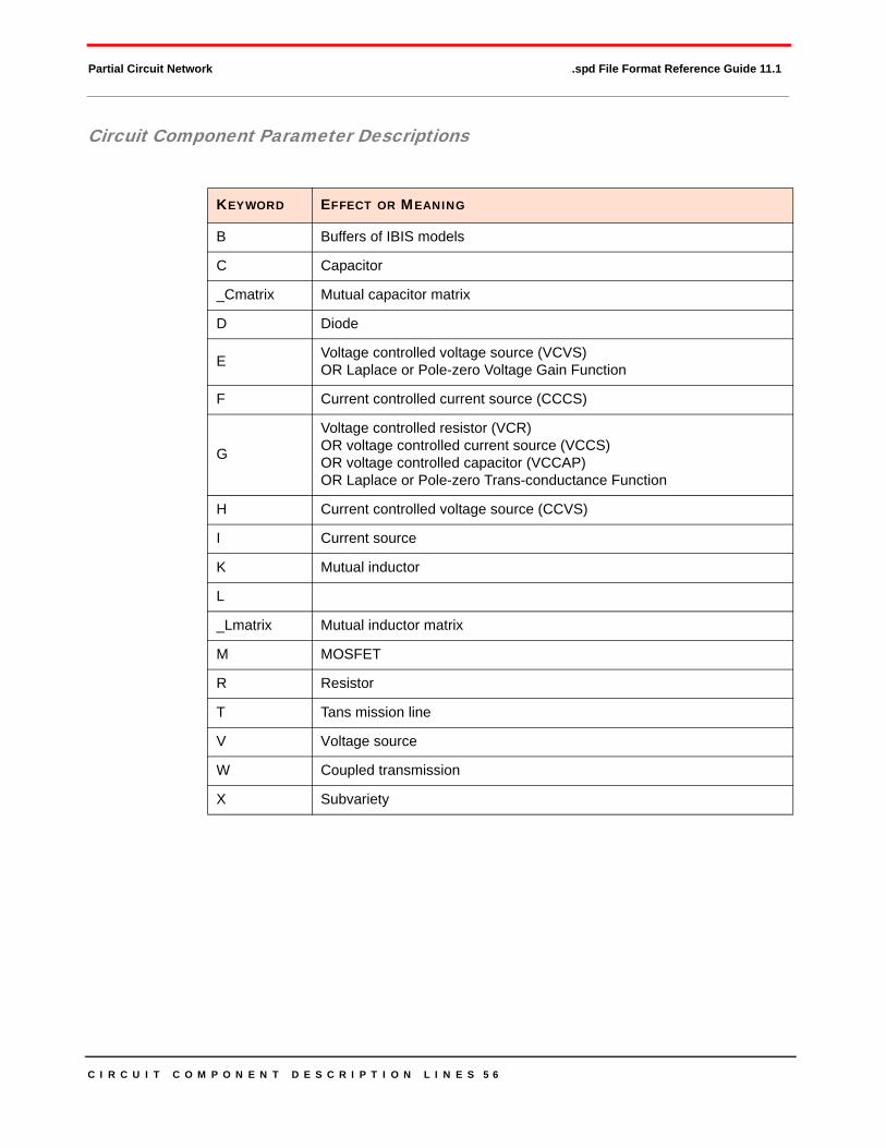
C I R C U I T C O M P O N E N T D E S C R I P T I O N L I N E S 5 6
Partial Circuit Network .spd File Format Reference Guide 11.1
Circuit Component Parameter Descriptions
KEYWORD EFFECT OR MEANING
B Buffers of IBIS models
C Capacitor
_Cmatrix Mutual capacitor matrix
D Diode
E Voltage controlled voltage source (VCVS)OR Laplace or Pole-zero Voltage Gain Function
F Current controlled current source (CCCS)
G
Voltage controlled resistor (VCR) OR voltage controlled current source (VCCS)OR voltage controlled capacitor (VCCAP)OR Laplace or Pole-zero Trans-conductance Function
H Current controlled voltage source (CCVS)
I Current source
K Mutual inductor
L
_Lmatrix Mutual inductor matrix
M MOSFET
R Resistor
T Tans mission line
V Voltage source
W Coupled transmission
X Subvariety

C I R C U I T C O M P O N E N T D E S C R I P T I O N L I N E S 5 7
Arbitrary Mathematical Expression Processing .spd File Format Reference Guide 11.1
ARBITRARY MATHEMATICAL EXPRESSION PROCESSINGA controlled component modeled with controlling variables and mathematical functions such as the Exponential function, Power function, etc. can be represented by a mathematical expression in Speed2000.
General Form for Arbitrary Mathematical Expression ProcessingA pair of single quotation marks enclose a valid mathematical expression. Letters in a given mathe-matical expression are case insensitive.
‘Mathematic_Expression’
In Speed2000, a valid mathematical expression is comprised of:
Constant numbersLocal and global defined parametersMathematical functionsMathematical operations• + addition
• - subtraction
• * multiplication
/ division Parentheses ( ) are used to establish precedence of operation within expressionsVoltage or current variables
NOTE! The math constant PI (Circumference / Diameter) is internally defined in Speed2000 as Pi = 3.14159265358979323846 ...

C I R C U I T C O M P O N E N T D E S C R I P T I O N L I N E S 5 8
Arbitrary Mathematical Expression Processing .spd File Format Reference Guide 11.1
Mathematical Expressions
Mathematical Expression Example10 * Exp ( - oef * V(pos, neg) )
Factor * Sqrt ( V(1) ^ 2.0 + V(2) ^ 2.0 )
Sin (2 * pi * freq )
FUNCTION MEANING COMMENT
sin(x) Sine function Specify x in radians
cos(x) Cosine function Specify x in radians
tan(x) Tangent function Specify x in radians.
asin(x) Arc Sine function The value is returned in radians|x| must be less than or equal to 1.0
acos(x) Arc Cosine function The value is returned in radians|x| must be less than or equal to 1.0
atan(x) Arc Tangent function The value is returned in radians
sinh(x) Hyperbolic Sine function Specify x in radians
cosh(x) Hyperbolic Cosine function Specify x in radians
tanh(x) Hyperbolic Tangent function Specify x in radians.The value is returned in radians
abs(x) Absolute Value function
sqrt(x) Square Root function x must be larger than or equal to zero
x ^ y Power function Example: 3^2 = 9
log(x) Natural Logarithm function x must be larger than zero
log10(x) Base 10 Logarithm function x must be larger than zero
exp(x) Exponential function

C I R C U I T C O M P O N E N T D E S C R I P T I O N L I N E S 5 9
Arbitrary Mathematical Expression Processing .spd File Format Reference Guide 11.1
Voltage VariablesA voltage variable stands for the voltage of one Circuit Node relative to another Circuit Node.
General FormV(node1, node2)
where the letter V (case insensitive).
The parentheses are required for a voltage variable expression.
The comma is required to separate the two Nodes.
Voltage Variable ExampleThe example represents the voltage difference by subtracting the voltage of node2 fromthe voltage of node1.
V(node1, node2) = V(node1)-V(node2)
This expression denotes the voltage of circuit node, node1, relative to circuit node,node2.
V(node1, node2)
Current VariableA current variable represents the current flowing through an independent voltage source.
Current flows from the positive Node to the negative Node.
Letter I — Required and is case insensitive
Parentheses — Required for a current variable
vsource — Name of an independent voltage source
Current Variable ExampleI(vsource)
NOTE!Voltage variables may not appear in math expressions for R, L and C components.
NOTE!Current variables may not appear in math expressions for R, L and C components.
The Current variable form is not presently used in any Speed2000 statements.
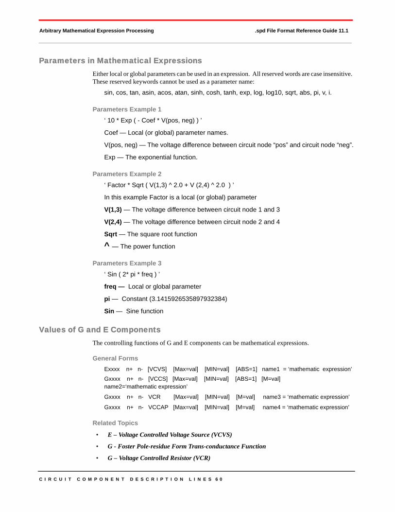
C I R C U I T C O M P O N E N T D E S C R I P T I O N L I N E S 6 0
Arbitrary Mathematical Expression Processing .spd File Format Reference Guide 11.1
Parameters in Mathematical ExpressionsEither local or global parameters can be used in an expression. All reserved words are case insensitive. These reserved keywords cannot be used as a parameter name:
sin, cos, tan, asin, acos, atan, sinh, cosh, tanh, exp, log, log10, sqrt, abs, pi, v, i.
Parameters Example 1‘ 10 * Exp ( - Coef * V(pos, neg) ) ’
Coef — Local (or global) parameter names.
V(pos, neg) — The voltage difference between circuit node “pos” and circuit node “neg”.
Exp — The exponential function.
Parameters Example 2‘ Factor * Sqrt ( V(1,3) ^ 2.0 + V (2,4) ^ 2.0 ) ’
In this example Factor is a local (or global) parameter
V(1,3) — The voltage difference between circuit node 1 and 3
V(2,4) — The voltage difference between circuit node 2 and 4
Sqrt — The square root function
^ — The power function
Parameters Example 3‘ Sin ( 2* pi * freq ) ’
freq — Local or global parameter
pi — Constant (3.1415926535897932384)
Sin — Sine function
Values of G and E ComponentsThe controlling functions of G and E components can be mathematical expressions.
General FormsExxxx n+ n- [VCVS] [Max=val] [MIN=val] [ABS=1] name1 = ‘mathematic expression’
Gxxxx n+ n- [VCCS] [Max=val] [MIN=val] [ABS=1] [M=val] name2=‘mathematic expression’
Gxxxx n+ n- VCR [Max=val] [MIN=val] [M=val] name3 = ‘mathematic expression’
Gxxxx n+ n- VCCAP [Max=val] [MIN=val] [M=val] name4 = ‘mathematic expression’
Related Topics
• E – Voltage Controlled Voltage Source (VCVS)
• G - Foster Pole-residue Form Trans-conductance Function
• G – Voltage Controlled Resistor (VCR)
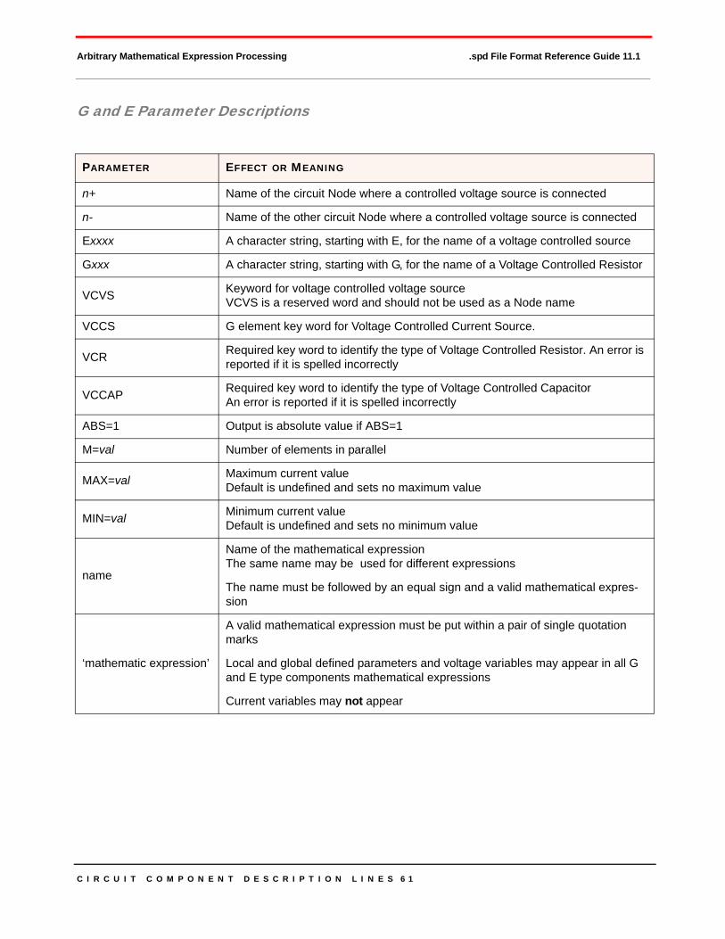
C I R C U I T C O M P O N E N T D E S C R I P T I O N L I N E S 6 1
Arbitrary Mathematical Expression Processing .spd File Format Reference Guide 11.1
G and E Parameter Descriptions
PARAMETER EFFECT OR MEANING
n+ Name of the circuit Node where a controlled voltage source is connected
n- Name of the other circuit Node where a controlled voltage source is connected
Exxxx A character string, starting with E, for the name of a voltage controlled source
Gxxx A character string, starting with G, for the name of a Voltage Controlled Resistor
VCVS Keyword for voltage controlled voltage sourceVCVS is a reserved word and should not be used as a Node name
VCCS G element key word for Voltage Controlled Current Source.
VCR Required key word to identify the type of Voltage Controlled Resistor. An error is reported if it is spelled incorrectly
VCCAP Required key word to identify the type of Voltage Controlled Capacitor An error is reported if it is spelled incorrectly
ABS=1 Output is absolute value if ABS=1
M=val Number of elements in parallel
MAX=val Maximum current value Default is undefined and sets no maximum value
MIN=val Minimum current value Default is undefined and sets no minimum value
name
Name of the mathematical expression The same name may be used for different expressions
The name must be followed by an equal sign and a valid mathematical expres-sion
‘mathematic expression’
A valid mathematical expression must be put within a pair of single quotation marks
Local and global defined parameters and voltage variables may appear in all G and E type components mathematical expressions
Current variables may not appear

C I R C U I T C O M P O N E N T D E S C R I P T I O N L I N E S 6 2
Arbitrary Mathematical Expression Processing .spd File Format Reference Guide 11.1
Values of R, L, and C ComponentsThe values of the R, L, and C components can be represented by mathematical expressions. These ex-pressions cannot contain voltage and current variables.
General FormRxxxx Node1 Node2 {Value | name = ‘mathematic expression’ }
Ixxxx Node1 Node2 [IC = f1] [R_0 = f2] {Value | name = ‘mathematic expression’}
Cxxxx Node1 Node2 [IC = f1] {Value | name = ‘mathematic expression’}
R, L, and C Components ExampleR1 1 2 R=’V0/I0’
Lx 3 4 ind=’L0/3’
C0 5 6 cap=’cap1+cap2’
In these examples, V0, I0, L0, cap1, and cap2 must be constant local/global parameters.
Related Topics
• Arbitrary Mathematical Expression Processing
• GC - Capacitor Description Line
• GC - Capacitor Description Line
• GC - Capacitor Description Line
R, L, and C Component Parameter Descriptions
PARAMETER EFFECT OR MEANING
Rxxxx A character string, starting with R, for the name of a resistor
Lxxxx A character string, starting with L, for the name of an inductor
Cxxxx A character string, starting with C, for the name of a capacitor
name Name of the mathematical expression The same name may be used for different expressions The name must be followed by an equal sign and a valid mathematical expression
‘mathematic expression’ A valid mathematical expression must be put within a pair of single quotation marks
Node1 Name of the circuit Node connected to one end of the inductor
Node2 Name of the circuit Node connected to the other end of the inductor
IC = f1 For an Inductor — Initial current flowing from Node1 to Node2 inside the inductor For a Capacitor — Initial voltage between Node1 and Node2 inside the capacitor
R_0 = f2 Resistance (for DC analysis). Default value: 0.0001 ohm

C I R C U I T C O M P O N E N T D E S C R I P T I O N L I N E S 6 3
Parameter Names .spd File Format Reference Guide 11.1
PARAMETER NAMESWhen defining parameter names, the following rules apply.
Parameter name consists of letters and numbers
First character must be a letter
There may be more than one .Param lines in .spd file
If value is not defined before it is used, Speed2000 prompts an error message.
The .Param lines must exist outside the data block enclosed by a pair of dots (‘.’) (Example .Param 1)
If the same parameter is defined as both a local and global parameter, the local parameter pre-cedes the global (Example .Param 2)
The order of parameter definitions is important. If a parameter is defined more than once, only the last definition of that parameter is effective (Parameter Order Example)
Example .Param 1.PARAM Cvalue=5p
.PARAM Rvalue=50
.PartialCkt RCload
R 1 2 Rvalue
C 1 2 Cvalue
.endPartialCkt
Example .Param 2.Param VCC=5V
.PartialCkt Source VCC=3V rvalue=50 rvalue=100
V pwr gnd VCC
R sig gnd rvalue
.EndP
In this example, the value of VCC is 3v, because the local parameter overwrites theglobal parameter. The value of rvalue is 100 because the latter definition overwrites theprevious value of 50.
Parameter Order Example.Param Rload = 100k
.Param Rload = 50k
The last definition of Rload with a value of 50k is used
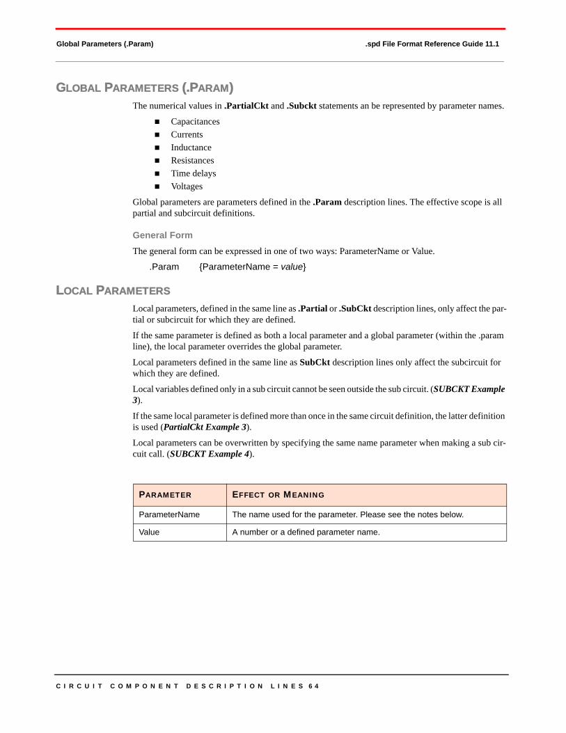
C I R C U I T C O M P O N E N T D E S C R I P T I O N L I N E S 6 4
Global Parameters (.Param) .spd File Format Reference Guide 11.1
GLOBAL PARAMETERS (.PARAM)The numerical values in .PartialCkt and .Subckt statements an be represented by parameter names.
CapacitancesCurrentsInductanceResistancesTime delaysVoltages
Global parameters are parameters defined in the .Param description lines. The effective scope is all partial and subcircuit definitions.
General FormThe general form can be expressed in one of two ways: ParameterName or Value.
.Param {ParameterName = value}
LOCAL PARAMETERSLocal parameters, defined in the same line as .Partial or .SubCkt description lines, only affect the par-tial or subcircuit for which they are defined.
If the same parameter is defined as both a local parameter and a global parameter (within the .param line), the local parameter overrides the global parameter.
Local parameters defined in the same line as SubCkt description lines only affect the subcircuit for which they are defined.
Local variables defined only in a sub circuit cannot be seen outside the sub circuit. (SUBCKT Example 3).
If the same local parameter is defined more than once in the same circuit definition, the latter definition is used (PartialCkt Example 3).
Local parameters can be overwritten by specifying the same name parameter when making a sub cir-cuit call. (SUBCKT Example 4).
PARAMETER EFFECT OR MEANING
ParameterName The name used for the parameter. Please see the notes below.
Value A number or a defined parameter name.

C I R C U I T C O M P O N E N T D E S C R I P T I O N L I N E S 6 5
Local Parameters .spd File Format Reference Guide 11.1
Local Parameter Descriptions
PARAMETER EFFECT OR MEANING
PartialCKTName A character string for the name of the partial circuit definition
IBIS=IBISFileName IBIS file name
Component=ComponentName
IBIS components. If more than one exists in the IBIS file, this clause might appear, otherwise the first component of the file is used
If spaces exist in the ComponentName field, it should be surrounded by single (‘ ’) or double (“ ”) quotes
PinName Specifies component pins of the IBIS file Options are set in the following parenthesis
ModelName Specifies the actual model the pin uses when the model name (given in the pin sec-tion) is a model selector
EnableSignal
Specifies the enable signal for the pin, if applicable
EnableSignal is a reserved word or the name of a sub-circuit definition, which a volt-age source is defined with a 0~1 volt
For this variable, the following are reserved words: Output, Input, and Output_High_Z
StimulusSignal
Specifies the stimulus signals. StimulusSignal is a reserved word or the name of a sub-circuit definition, which a voltage source is defined with a 0~1 voltage
For this variable, the following are reserved words: Stuck_High, Stuck_Low

C I R C U I T C O M P O N E N T D E S C R I P T I O N L I N E S 6 6
Partial Circuit Command .spd File Format Reference Guide 11.1
PARTIAL CIRCUIT COMMAND
General Form.PartialCkt PartialCKTDefName [TYPE=HSPICE] [ExtNode={NodeName}] [{ParameterName =ParameterValue}]
Partial Circuit End Line Example.EndPartialCkt [PartialCKTDefName]
[IBIS=IBISFilename [Component=ComponentName]]
[{PinName = ( [ModelName] [, [typ] [, [EnableSignal] [, [StimulusSignal] [, [ramp_fwf]
[, [ramp_rwf] [, [c_com_pu] [, [c_com_pd] [, [c_com_pc] [, [c_com_gc] ] ] ] ] ] ] ] ] ] } ]
PartialCkt Example 1 .PartialCkt DR_50mV1 1 0 PWL FILE=source_per.datRS 1 2 28.0.EndPartialCkt
.PartialCkt R28R1 1 0 28.EndPartialCkt
.PartialCkt DecapC1 0 2 0.047uL1 2 3 0.9nR1 3 1 844m.EndPartialCkt
PartialCktExample 2 .PartialCkt Load rvalue1=30 rvalue2=50Rload1 1 2 rvalue1Rload2 2 3 rvalue2.EndP
PartialCkt Example 3 .Param VCC=5V.PartialCkt Source VCC=3V rvalue=50 rvalue=100V pwr gnd VCCR sig gnd rvalue.EndP
In PartialCkt Example 3, the value of VCC is 3V because the local parameter assignment over-rides the global assignment (within the .param line).
The value of rvalue is 100 because the latter local parameter overwrites the previously assignedlocal parameter.
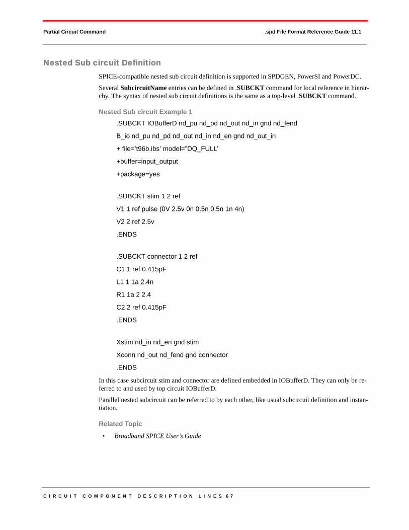
C I R C U I T C O M P O N E N T D E S C R I P T I O N L I N E S 6 7
Partial Circuit Command .spd File Format Reference Guide 11.1
Nested Sub circuit DefinitionSPICE-compatible nested sub circuit definition is supported in SPDGEN, PowerSI and PowerDC.
Several SubcircuitName entries can be defined in .SUBCKT command for local reference in hierar-chy. The syntax of nested sub circuit definitions is the same as a top-level .SUBCKT command.
Nested Sub circuit Example 1 .SUBCKT IOBufferD nd_pu nd_pd nd_out nd_in gnd nd_fend
B_io nd_pu nd_pd nd_out nd_in nd_en gnd nd_out_in
+ file=’t96b.ibs’ model=”DQ_FULL’
+buffer=input_output
+package=yes
.SUBCKT stim 1 2 ref
V1 1 ref pulse (0V 2.5v 0n 0.5n 0.5n 1n 4n)
V2 2 ref 2.5v
.ENDS
.SUBCKT connector 1 2 ref
C1 1 ref 0.415pF
L1 1 1a 2.4n
R1 1a 2 2.4
C2 2 ref 0.415pF
.ENDS
Xstim nd_in nd_en gnd stim
Xconn nd_out nd_fend gnd connector
.ENDS
In this case subcircuit stim and connector are defined embedded in IOBufferD. They can only be re-ferred to and used by top circuit IOBufferD.
Parallel nested subcircuit can be referred to by each other, like usual subcircuit definition and instan-tiation.
Related Topic
• Broadband SPICE User’s Guide
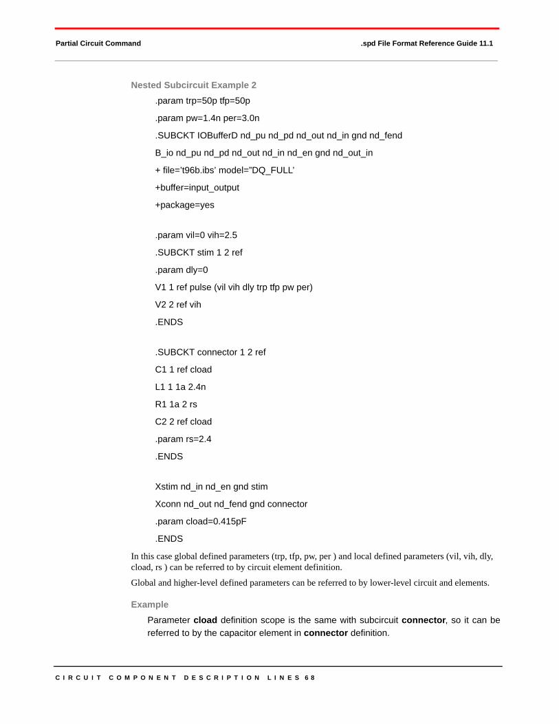
C I R C U I T C O M P O N E N T D E S C R I P T I O N L I N E S 6 8
Partial Circuit Command .spd File Format Reference Guide 11.1
Nested Subcircuit Example 2 .param trp=50p tfp=50p
.param pw=1.4n per=3.0n
.SUBCKT IOBufferD nd_pu nd_pd nd_out nd_in gnd nd_fend
B_io nd_pu nd_pd nd_out nd_in nd_en gnd nd_out_in
+ file=’t96b.ibs’ model=”DQ_FULL’
+buffer=input_output
+package=yes
.param vil=0 vih=2.5
.SUBCKT stim 1 2 ref
.param dly=0
V1 1 ref pulse (vil vih dly trp tfp pw per)
V2 2 ref vih
.ENDS
.SUBCKT connector 1 2 ref
C1 1 ref cload
L1 1 1a 2.4n
R1 1a 2 rs
C2 2 ref cload
.param rs=2.4
.ENDS
Xstim nd_in nd_en gnd stim
Xconn nd_out nd_fend gnd connector
.param cload=0.415pF
.ENDS
In this case global defined parameters (trp, tfp, pw, per ) and local defined parameters (vil, vih, dly, cload, rs ) can be referred to by circuit element definition.
Global and higher-level defined parameters can be referred to by lower-level circuit and elements.
ExampleParameter cload definition scope is the same with subcircuit connector, so it can bereferred to by the capacitor element in connector definition.
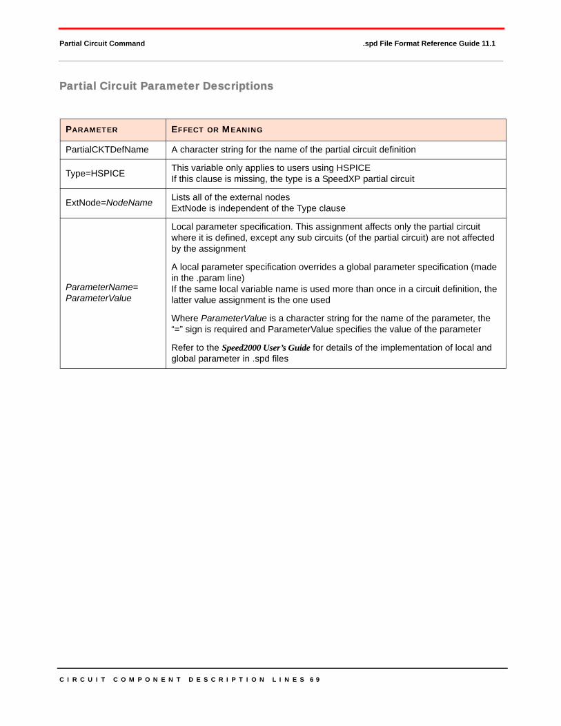
C I R C U I T C O M P O N E N T D E S C R I P T I O N L I N E S 6 9
Partial Circuit Command .spd File Format Reference Guide 11.1
Partial Circuit Parameter Descriptions
PARAMETER EFFECT OR MEANING
PartialCKTDefName A character string for the name of the partial circuit definition
Type=HSPICE This variable only applies to users using HSPICE If this clause is missing, the type is a SpeedXP partial circuit
ExtNode=NodeName Lists all of the external nodes ExtNode is independent of the Type clause
ParameterName=ParameterValue
Local parameter specification. This assignment affects only the partial circuit where it is defined, except any sub circuits (of the partial circuit) are not affected by the assignment
A local parameter specification overrides a global parameter specification (made in the .param line) If the same local variable name is used more than once in a circuit definition, the latter value assignment is the one used
Where ParameterValue is a character string for the name of the parameter, the “=” sign is required and ParameterValue specifies the value of the parameter
Refer to the Speed2000 User’s Guide for details of the implementation of local and global parameter in .spd files

C I R C U I T C O M P O N E N T D E S C R I P T I O N L I N E S 7 0
.Connect - Circuit Package Connection Lines .spd File Format Reference Guide 11.1
.CONNECT - CIRCUIT PACKAGE CONNECTION LINESThe partial circuit connection description lines starts with the command .Connect. It ends with the command .EndC.
Between .Connect and .EndC are the specifications of connections between circuit nodes and pack-age nodes.
The .Connect line establishes a partial circuit name corresponding to a partial circuit definition.
General Form.Connect PartialCKTName PartialCKTDefName [Absent] [Usage=nnnn]
General Form.EndC PartialCKTName
PartialCKTName
PartialCKTName is a character string for the name of the physical partial circuit network. The lineindicates the end of partial circuit calls
Circuit Package Connection Parameters
PARAMETER EFFECT OR MEANING
.Connect Keyword for .Connect line
PartialCKTName A character string for the partial circuit name
PartialCKTDefName A character string for the name of the partial circuit definition given in the .PartialCKT command
Absent1When present, it means a circuit will not be considered in the simulation and every bit triplet is set to 001
nnnn
A number, in any system:
• Decimal
• Hexadecimal (format: 0xnnnn or 0Xnnnn)
• Octal (format: 0nnnn)
• Binary (format: 0bnnnn or 0Bnnnn)
This number, once translated into its binary counterpart, governs the usage in each tool.
1. The highest precedence keyword. It supersedes the usage flag.

C I R C U I T C O M P O N E N T D E S C R I P T I O N L I N E S 7 1
.Model Description Line .spd File Format Reference Guide 11.1
.MODEL DESCRIPTION LINEThe statement should appear before all .PartialCkt and .Subckt definitions. This statement currently works with the modeling feature of Speed2000. It is only available in Speed2000.
CapacitorCoupled transmission lineDiodeMOSFETResistorSmall signal parameter data frequency tableS parameter
General Form.MODEL ModelName ModelType [pname1 = val1 pname2 = val2 ...]
Model Diode Example.MODEL Diode1 D IS=1E-13 N=1.05
Model Parameter Descriptions
PARAMETER EFFECT OR MEANING
ModelName Model name
ModelType
C: CapacitorD: DiodeNMOS: n-type MOSFETPMOS: p-type MOSFETR: ResistorW: Coupled transmission lineS: S parameters
pname1, pname2, ...
Model parameter names. Parameter names for different types of models may be different
val1, val2, ... Model parameter values
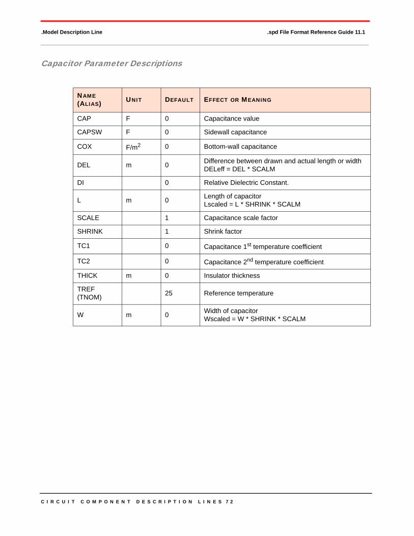
C I R C U I T C O M P O N E N T D E S C R I P T I O N L I N E S 7 2
.Model Description Line .spd File Format Reference Guide 11.1
Capacitor Parameter Descriptions
NAME (ALIAS) UNIT DEFAULT EFFECT OR MEANING
CAP F 0 Capacitance value
CAPSW F 0 Sidewall capacitance
COX F/m2 0 Bottom-wall capacitance
DEL m 0 Difference between drawn and actual length or widthDELeff = DEL * SCALM
DI 0 Relative Dielectric Constant.
L m 0 Length of capacitorLscaled = L * SHRINK * SCALM
SCALE 1 Capacitance scale factor
SHRINK 1 Shrink factor
TC1 0 Capacitance 1st temperature coefficient
TC2 0 Capacitance 2nd temperature coefficient
THICK m 0 Insulator thickness
TREF (TNOM) 25 Reference temperature
W m 0 Width of capacitor Wscaled = W * SHRINK * SCALM

C I R C U I T C O M P O N E N T D E S C R I P T I O N L I N E S 7 3
.Model Description Line .spd File Format Reference Guide 11.1
Diode Parameter DescriptionsFor ModelType D (Diode), the following parameter names are used.
NAME (ALIAS) UNIT DEFAULT EFFECT OR MEANING
Diode DC Parameter
LEVEL 1
Diode model selectorLEVEL=1Selects the non-geometric junction diode model LEVEL=3Selects the geometric junction diode model
AREALEVEL=1 UnitlessLEVEL=3 m2
1.0
Junction Area LEVEL=1 AREAeff = AREA * MLEVEL=3 AREAeff = AREA * SCALM2 * SHRINK2 * MIf L and W is given AREAeff = Weff * Leff * M
PJLEVEL=1 UnitlessLEVEL=3 m
0.0
Junction peripheryLEVEL = 1 PJeff = PJ * MLEVEL = 3 PJeff = PJ * SCALM * SHRINK * M If L and W is given PJeff = (2 * Weff + 2 * Leff) * M
EXPLI amp/AREAeff 0.0
Forward current explosion parameter. The i-v characteristics are linear with the slope at the explosion point, when diode cur-rent is larger than EXPLleff EXPLleff = EXPLI * AREAeff
EXPLIR amp/AREAeff 0.0
Reverse current explosion parameter. The i-v characteristics are linear with the slope at the explosion point, when diode cur-rent is less then --- EXPLReff EXPLIReff = EXPLIR * AREAeff
IB (IBV) amp/AREAeff 1.0e-3Current when vd = breakdown voltageIBeff = IB / SCALM2 * AREAeff
IK (IKF, JBF) amp/AREAeff 0.0 Forward knee current. IKeff = IK * AREAeff
IK (JBR) amp/AREAeff 0.0 Reverse knee current. IKReff =IKR * AREAeff
IS (JS) amp/AREAeff
LEVEL=1 1.0e-14LEVEL=3 0.0
Saturation current per unit area. If ISeff is less than EPSMIN, ISeff will be set to EPSMIN LEVEL = 1 ISeff = IS * AREAeffLEVEL = 3 IS / SCALM2 * AREAeff
JSW (ISP) amp/PJeff 0.0
Sidewall saturation current per unit pj. If ISWeff is less than EPSMIN, ISWeff is set to EPSMIN LEVEL =1 JSWeff = JSW * PJeffLEVEL= 3 JSWeff = JSW / SCALM * PJeff
L m 0.0 Length of the diodeLeff = L * SHRINK * SCALM + XWeff
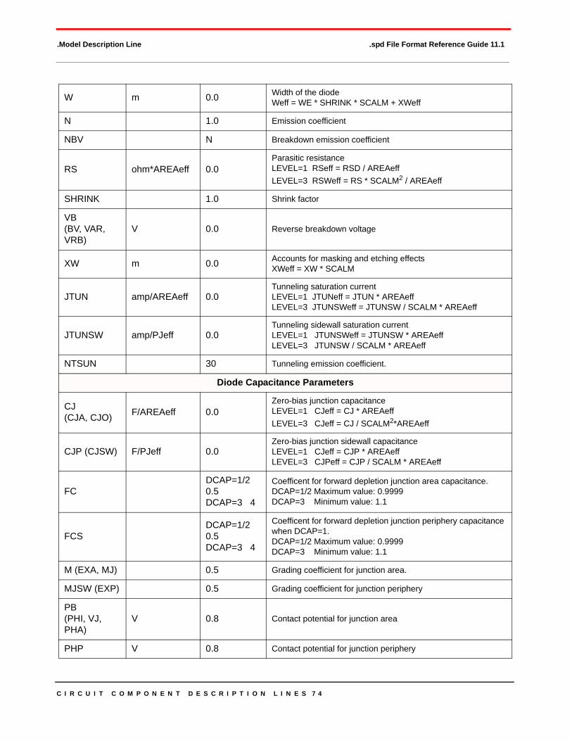
C I R C U I T C O M P O N E N T D E S C R I P T I O N L I N E S 7 4
.Model Description Line .spd File Format Reference Guide 11.1
W m 0.0 Width of the diodeWeff = WE * SHRINK * SCALM + XWeff
N 1.0 Emission coefficient
NBV N Breakdown emission coefficient
RS ohm*AREAeff 0.0Parasitic resistanceLEVEL=1 RSeff = RSD / AREAeffLEVEL=3 RSWeff = RS * SCALM2 / AREAeff
SHRINK 1.0 Shrink factor
VB (BV, VAR, VRB)
V 0.0 Reverse breakdown voltage
XW m 0.0 Accounts for masking and etching effects XWeff = XW * SCALM
JTUN amp/AREAeff 0.0Tunneling saturation currentLEVEL=1 JTUNeff = JTUN * AREAeffLEVEL=3 JTUNSWeff = JTUNSW / SCALM * AREAeff
JTUNSW amp/PJeff 0.0Tunneling sidewall saturation currentLEVEL=1 JTUNSWeff = JTUNSW * AREAeffLEVEL=3 JTUNSW / SCALM * AREAeff
NTSUN 30 Tunneling emission coefficient.
Diode Capacitance Parameters
CJ (CJA, CJO) F/AREAeff 0.0
Zero-bias junction capacitanceLEVEL=1 CJeff = CJ * AREAeffLEVEL=3 CJeff = CJ / SCALM2*AREAeff
CJP (CJSW) F/PJeff 0.0Zero-bias junction sidewall capacitanceLEVEL=1 CJeff = CJP * AREAeffLEVEL=3 CJPeff = CJP / SCALM * AREAeff
FCDCAP=1/2 0.5DCAP=3 4
Coefficent for forward depletion junction area capacitance.DCAP=1/2 Maximum value: 0.9999DCAP=3 Minimum value: 1.1
FCSDCAP=1/2 0.5DCAP=3 4
Coefficent for forward depletion junction periphery capacitance when DCAP=1.DCAP=1/2 Maximum value: 0.9999DCAP=3 Minimum value: 1.1
M (EXA, MJ) 0.5 Grading coefficient for junction area.
MJSW (EXP) 0.5 Grading coefficient for junction periphery
PB (PHI, VJ, PHA)
V 0.8 Contact potential for junction area
PHP V 0.8 Contact potential for junction periphery

C I R C U I T C O M P O N E N T D E S C R I P T I O N L I N E S 7 5
.Model Description Line .spd File Format Reference Guide 11.1
TT S 0.0 Transit time.
Metal and Poly Capacitor for LEVEL = 3 Diode
LM m 0.0 Length of metal LMeff = LM * SCALM * SHRINK
WM m 0.0 Width of metal WMeff = WM * SCALM * SHRINK
LP m 0.0 Length of poly LPeff = LP * SCALM * SHRINK
WP m 0.0 Width of Poly.WPeff = WP * SCALM * SHRINK
XOI 10k Thickness of the poly oxide
XOM 10k Thickness of the metal oxide
XM m 0.0 Accounts for masking and etching effect in metal XMeff = XM * SCALM
XP m 0.0 Accounts for masking and etching effect in poly XPeff = XP * SCALM
Temperature Effects Parameters
CTA 1/K 0.0 Temperature effect parameter for CJ
CTP 1/K 0.0 Temperature effect parameter for CJP
EG eV
TLEV=0,1 1.11TLEV=2 1.16
Energy gap
GAP1 eV/K 7.02e-4 First bandgap correction factor
GAP2 1108 Second bandgap correction factor
TCV 1/K 0.0 Temperature effect parameter for BV
TLEV 0.0 Temperature equation selector. Work together with TLEVC
TLEVC 0.0 Temperature equation selector. Work together with TLEV.
TM1 1/K 0.0 First temperature effect parameter fro M
TM2 1/K2 0.0 Second temperature effect parameter for M
TPB V/K 0.0 Temperature effect parameter for PB
TPHP V/K 0.0 Temperature effect parameter for PHP
TREF (TNOM) C 25.0 Model nominal temperature
TRS 1/K 0.0 Temperature effect parameter for RS
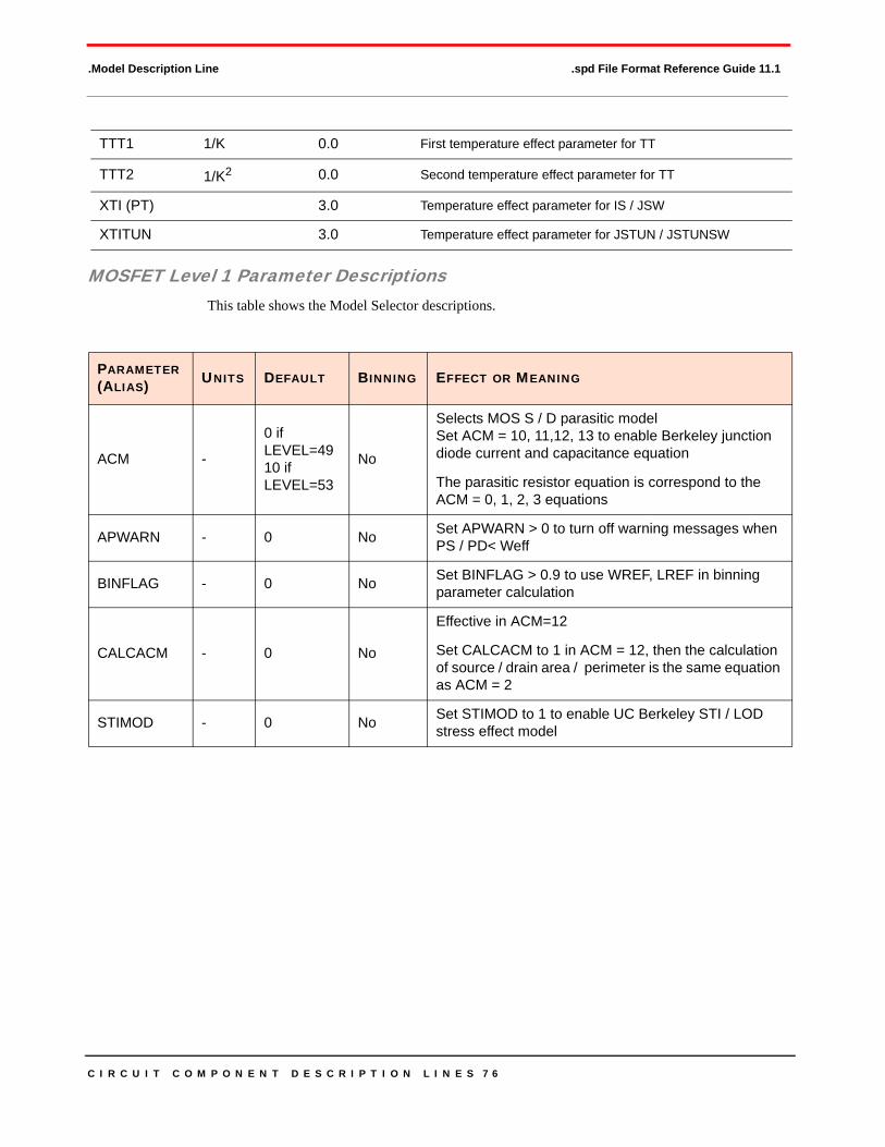
C I R C U I T C O M P O N E N T D E S C R I P T I O N L I N E S 7 6
.Model Description Line .spd File Format Reference Guide 11.1
MOSFET Level 1 Parameter DescriptionsThis table shows the Model Selector descriptions.
TTT1 1/K 0.0 First temperature effect parameter for TT
TTT2 1/K2 0.0 Second temperature effect parameter for TT
XTI (PT) 3.0 Temperature effect parameter for IS / JSW
XTITUN 3.0 Temperature effect parameter for JSTUN / JSTUNSW
PARAMETER (ALIAS) UNITS DEFAULT BINNING EFFECT OR MEANING
ACM -
0 if LEVEL=4910 if LEVEL=53
No
Selects MOS S / D parasitic model Set ACM = 10, 11,12, 13 to enable Berkeley junction diode current and capacitance equation
The parasitic resistor equation is correspond to the ACM = 0, 1, 2, 3 equations
APWARN - 0 No Set APWARN > 0 to turn off warning messages when PS / PD< Weff
BINFLAG - 0 No Set BINFLAG > 0.9 to use WREF, LREF in binning parameter calculation
CALCACM - 0 No
Effective in ACM=12
Set CALCACM to 1 in ACM = 12, then the calculation of source / drain area / perimeter is the same equation as ACM = 2
STIMOD - 0 No Set STIMOD to 1 to enable UC Berkeley STI / LOD stress effect model
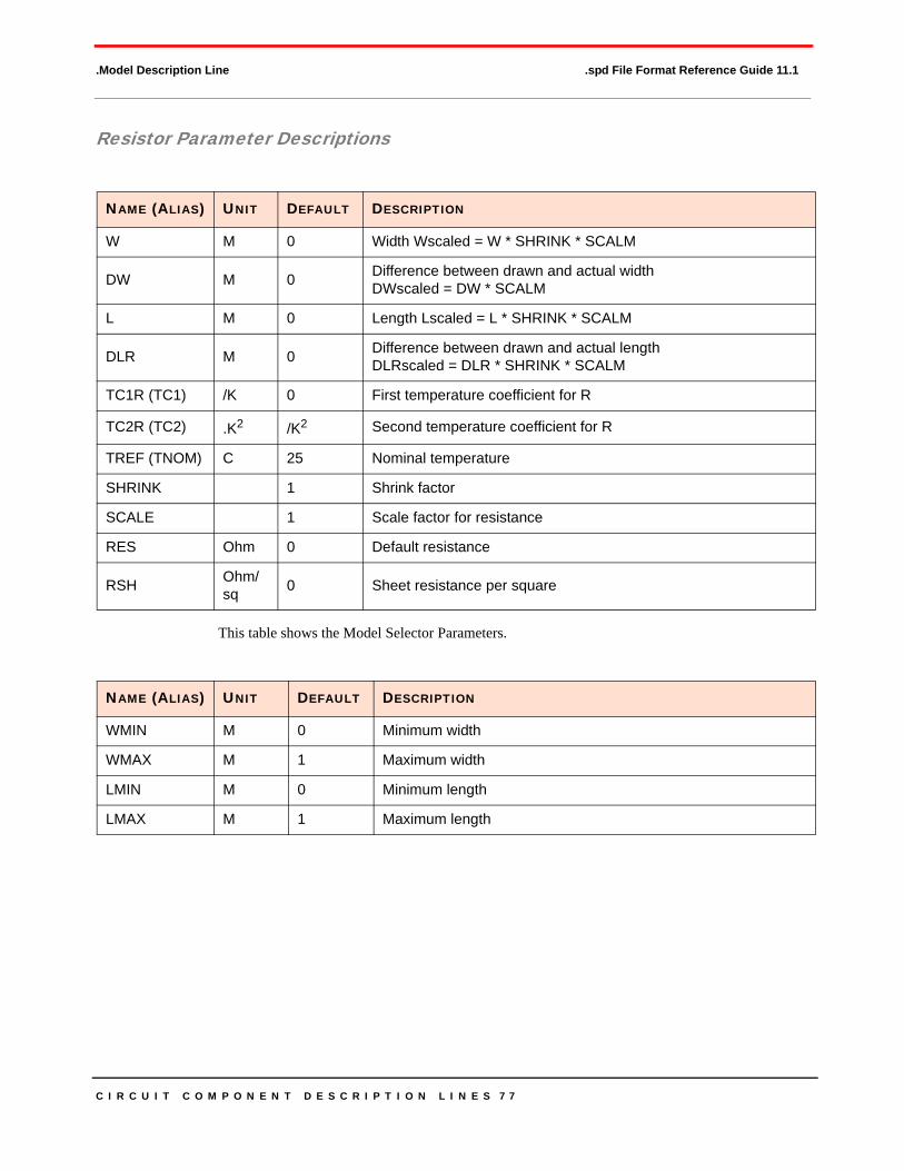
C I R C U I T C O M P O N E N T D E S C R I P T I O N L I N E S 7 7
.Model Description Line .spd File Format Reference Guide 11.1
Resistor Parameter Descriptions
This table shows the Model Selector Parameters.
NAME (ALIAS) UNIT DEFAULT DESCRIPTION
W M 0 Width Wscaled = W * SHRINK * SCALM
DW M 0 Difference between drawn and actual width DWscaled = DW * SCALM
L M 0 Length Lscaled = L * SHRINK * SCALM
DLR M 0 Difference between drawn and actual length DLRscaled = DLR * SHRINK * SCALM
TC1R (TC1) /K 0 First temperature coefficient for R
TC2R (TC2) .K2 /K2 Second temperature coefficient for R
TREF (TNOM) C 25 Nominal temperature
SHRINK 1 Shrink factor
SCALE 1 Scale factor for resistance
RES Ohm 0 Default resistance
RSH Ohm/sq 0 Sheet resistance per square
NAME (ALIAS) UNIT DEFAULT DESCRIPTION
WMIN M 0 Minimum width
WMAX M 1 Maximum width
LMIN M 0 Minimum length
LMAX M 1 Maximum length

C I R C U I T C O M P O N E N T D E S C R I P T I O N L I N E S 7 8
.Model Description Line .spd File Format Reference Guide 11.1
Small Signal Parameter Data Frequency Table Model (SP Model)
PARAMETERS EFFECT OR MEANING
Name Model name
N Matrix dimension. Default = 1
FSTART Starting frequency point for data. Default = 0
FSTOP Final frequency point for date. Use this parameter only for the LINEAR and LOG spacing formats.
NINumber of frequency points per intervalUse this parameter only for the DEC and OCT spacing formats Default = 10
SPACING
Data sample spacing format:• LIN (LINEAR): Uniform spacing with frequency step of (FSTOP-FSTART_/(npts-1)
Default
• OCT: Octave variation with FSTART as the starting frequency and NI points per octave NPTS (See parameter DATA) sets the final frequency
• DEC: Decade variation with FSTART as the starting frequency and NI points per decade NPTS sets the final frequency
• LOG: Logarithmic spacing. FSTART and FSTOP are the starting and final frequencies
• POI: Non-uniform spacing. Pairs data
• (NONUNIFORM) points with frequency points
MATRIX
Matrix (data point) format:
• SYMMETRIC: Symmetric matrix. Specifies only lower-half triangle of a matrix (default)
• HERMITIAN: Similar to SYMMETRIC; Off-diagonal terms are complex-conjugates of each other
• NONSYMMETRIC: Non-symmetric (full) matrix
• VALTYPE Data type of matrix elements:
• REAL: Real entry • CARTESIAN: Complex number in real/imaginary format (default) • POLAR: Complex number in polar format. Specify angles in radians
INFINITYData point at infinity. Typically real-valued. This data format must be consistent with MATRIX and VALTYPE specifications. NPTS does not count this point.
INTERPOLATION
Interpolation scheme:
• STEP: Piecewise step. Default
• LINEAR: Piecewise linear
• SPLINE: B-spline curve fit
Note: Interpolation and extrapolation occur after the simulator internally converts the Z and S-parameter data to Y-parameter data

C I R C U I T C O M P O N E N T D E S C R I P T I O N L I N E S 7 9
.Model Description Line .spd File Format Reference Guide 11.1
Coupled Transmission Lines Parameters for ModelType W
Coupled Transmission Lines Example.Model example_rlc W MODELTYPE=RLGC N=3
+ Lo =
+ 2.311e-6
+ 4.14e-7 2.988e-6
+ 8.42e-8 5.27e-7 2.813e-6
+Co =
+ 2.392e-11
+ -1.08e-12 -5.72e-12 2.447e-11
+ Ro =
+ 42.5
+ 0 41.0
+ 0 0 33.5
+ Rs =
+ 0.00135
+ 0 0.001303
+ 0 0 0.001064
+ Go =
+ 0.000609
+ -0.0001419 0.000599
+ -0.00002323 -0.00009 0.000502
+ Gd =
+ 5.242e- 13
+ -1.221e-13 5.164e- 13
+ -1.999e- 14 -7.747e- 14 4.321e- 13
PARAMETERS EFFECT OR MEANING
N Number of conductors
L Lower triangular part of DC inductance matrix, per unit length (H/m)
C Lower triangular part of DC capacitance matrix, per unit length (F | m)
Ro Lower triangular part of DC resistance matrix, per unit length (Ω | m)
Go Lower triangular part of DC shunt conductance matrix, per unit length (S | m)
Rs Lower triangular part of skin effect resistance matrix, per unit length .
Gd Lower triangle part of Dielectric loss conductance matrix, per unit length .

C I R C U I T C O M P O N E N T D E S C R I P T I O N L I N E S 8 0
.Model Description Line .spd File Format Reference Guide 11.1
Tabular W Model
To ensure accuracy, the W-element tabular model requires the following:
1. R and G tables require zero frequency points. To specify a zero point, you may use DC keyword or f=0 data entry in the DATA field of the SP model.
2. L and C tables require infinity frequency points as well as zero frequency points. To specify an infinity frequency point, use the INFINITy keyword of the SP model.
Tabular ExampleMODEL W_model W MODEL TYPE=TABLE
+ N=4
+ LMODEL = l_SPmodel CMODEL = c_SPmodel
+ RMODEL = r_SPmodel GMODEL = g_SPmodel
S Parameter DescriptionsThe following parameter names are used for ModelType S.
PARAMETERS EFFECT OR MEANING
N Number of signal conductors
LMODEL SP model name for the inductance matrix array
CMODEL SP model name for the capacitance matrix array
RLMODEL SP model name fro the resistance matrix array. Default zero
GMODEL SP model name for the conductance matrix array. Default zero
PARAMETERS EFFECT OR MEANING
RFMFILE RMF file name
BNPFILE BNP file name
TSTONEFILE TOUTCHSTONE file name
Fmax Max frequency of inverse Fourier Transform when using BNP or TOUCHSTONE files Default Fmax = 1 / (simulation time interval)
Fbase The base frequency of inverse Fourier Transform when using BNP or TOUCHSTONE files Default Fbase = 1 / (simulation period)

C I R C U I T C O M P O N E N T D E S C R I P T I O N L I N E S 8 1
.Model Description Line .spd File Format Reference Guide 11.1
S Parameters ExampleModel example_S1 S+ TSTONEFILE = example_s.s2p
Model example_S2 S
+ RFMFILE= example_s.rmf+Fmax = 15g+Fbase = 250 Meg
Model example_S3 S+BNPFILE=example_s.bnp+Fmax = 15g+Fbase = 250Meg
Bulk to Source / Drain Diodes - DC Part Parameters
PARAMETER (ALIAS) UNITS DEFAULT EFFECT OR MEANING
ACM - 0 Selects MOS S/D parasitics model. ACM=0 is SPICE style Use ACM=2 or 3 for LDD
JS A/m2 0Bulk Junction saturation current JSscaled=JS/SCALM2
For ACM=1 unit is A/m and JSscaled=JS/SCALM
JSW A/m 0 Sidewalk bulk junction saturation current: JSWscaled=JSWSCALM
IS A 1e-14 Bulk junction saturation current
N - 1 Emission coefficient
NDS - 1 Reverse bias slope coefficient
VNDS V -1 Reverse diode current transition point

C I R C U I T C O M P O N E N T D E S C R I P T I O N L I N E S 8 2
.Model Description Line .spd File Format Reference Guide 11.1
Bulk to Source / Drain Diodes - Capacitance Part Parameters
PARAMETER (ALIAS) UNITS DEFAULT EFFECT OR MEANING
CBD F 0 Zero bias bulk-drain junction capacitance Used only if CJ and CJSW are 0.0
CBS F 0 Zero bias bulk-source junction capacitance Use only if CJ and CJSW are 0.0
CJ (CBD, CSB, CJA) F/m2 579.11uF/m2
Zero-bias bulk junction capacitance: CJscaled = CJ / SCALM2
For ACM = 1 the unit is F / m CJscaled = CJSW / SCALM
CJSW (CJP) F/m2 0.0 Zero-bias sidewalk bulk junction capacitance CJSWscaled = CJGASW / SCALM
CJGAE F/m CJSWZero-bias gate-edge sidewalk bulk junction capacitance (ACM = 3 only) CJGATEscaled = CJGATE / SCALM
FC - 0.5 Forward bias depletion capacitance coefficient (not used in MOS diode calculation)
MJ (EXA, EXJ, EXS, EXD) - 0.5 Source / drain bulk junction grading coefficient
MJSW (EXP) - 0.33 Sidewall junction grading coefficient
PB(PHA, PHS, PHD) V 0.8 Source / drain bulk junction potential
PHP V PB Sidewall junction potential
TT s 0 Transit time
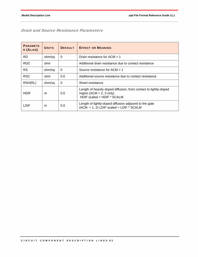
C I R C U I T C O M P O N E N T D E S C R I P T I O N L I N E S 8 3
.Model Description Line .spd File Format Reference Guide 11.1
Drain and Source Resistance Parameters
PARAMETER (ALIAS) UNITS DEFAULT EFFECT OR MEANING
RD ohm/sq 0 Drain resistance for ACM > 1
RDC ohm Additional drain resistance due to contact resistance
RS ohm/sq 0 Source resistance for ACM > 1
RSC ohm 0.0 Additional source resistance due to contact resistance
RSH(RL) ohm/sq 0 Sheet resistance
HDIF m 0.0Length of heavily-doped diffusion, from contact to lightly-doped region (ACM = 2, 3 only) HDIF scaled = HDIF * SCALM
LDIF m 0.0 Length of lightly-doped diffusion adjacent to the gate (ACM = 1, 2) LDIF scaled = LDIF * SCALM
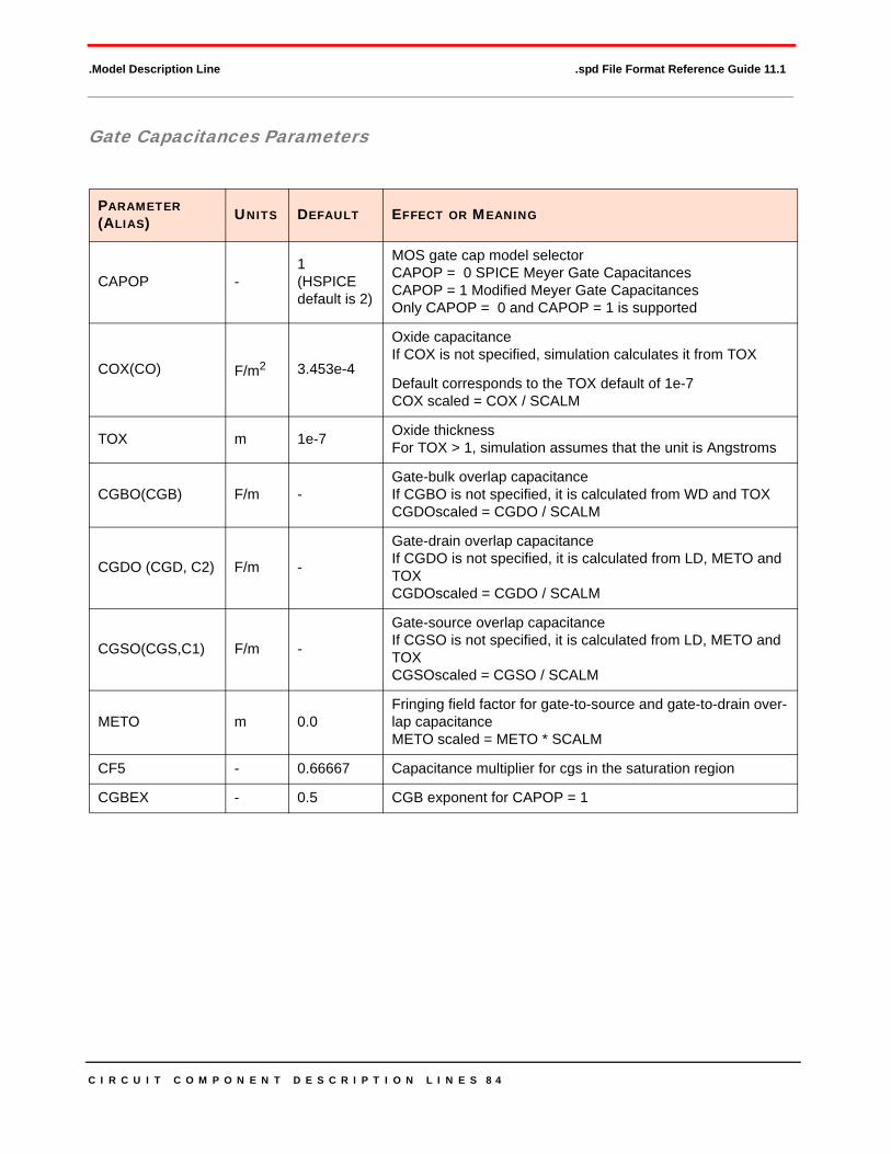
C I R C U I T C O M P O N E N T D E S C R I P T I O N L I N E S 8 4
.Model Description Line .spd File Format Reference Guide 11.1
Gate Capacitances Parameters
PARAMETER (ALIAS) UNITS DEFAULT EFFECT OR MEANING
CAPOP -1(HSPICE default is 2)
MOS gate cap model selector CAPOP = 0 SPICE Meyer Gate Capacitances CAPOP = 1 Modified Meyer Gate Capacitances Only CAPOP = 0 and CAPOP = 1 is supported
COX(CO) F/m2 3.453e-4
Oxide capacitance If COX is not specified, simulation calculates it from TOX
Default corresponds to the TOX default of 1e-7 COX scaled = COX / SCALM
TOX m 1e-7 Oxide thickness For TOX > 1, simulation assumes that the unit is Angstroms
CGBO(CGB) F/m -Gate-bulk overlap capacitance If CGBO is not specified, it is calculated from WD and TOX CGDOscaled = CGDO / SCALM
CGDO (CGD, C2) F/m -
Gate-drain overlap capacitance If CGDO is not specified, it is calculated from LD, METO and TOX CGDOscaled = CGDO / SCALM
CGSO(CGS,C1) F/m -
Gate-source overlap capacitance If CGSO is not specified, it is calculated from LD, METO and TOX CGSOscaled = CGSO / SCALM
METO m 0.0Fringing field factor for gate-to-source and gate-to-drain over-lap capacitance METO scaled = METO * SCALM
CF5 - 0.66667 Capacitance multiplier for cgs in the saturation region
CGBEX - 0.5 CGB exponent for CAPOP = 1

C I R C U I T C O M P O N E N T D E S C R I P T I O N L I N E S 8 5
.Model Description Line .spd File Format Reference Guide 11.1
Effective Length and Width Parameters
PARAMETER (ALIAS) UNITS DEFAULT EFFECT OR MEANING
DEL m 0.0 Channel length reduction on each side DELscaled = DEL * SCALM
LMLT - 1.0 Gate length shrink factor.
LD (DLT, LATD) m 0.75XJLateral diffusion into the channel from the source and the drain diffusion LDscaled = LD * SCALM
LREF m 0.0 Channel length reference LREFscaled = LREF * SCALM
WD m 0.0 Lateral diffusion into the channel from the bulk along the width WDscaled = WD * SCALM
WMLT - 1.0 Diffusion layer and width shrink factor
WREF m 0.0 Channel width reference WREFscaled = WREF * SCALM
XJ m 0.0 Metallurgical junction depth XJscaled = XJ*SCALM
XL(DL,LDEL) m 0.0 Length bias accounts for the masking and etching effects.XLscaled = XL * SCALM.
XLREF m 0.0Difference between the physical (on the wafer) and the drawn reference channel length XLREFscaled = XLREF * SCALM
XW m 0.0Difference between the physical (on the wafer) and the drawn S / D active width XWscaled = XW * SCALM
XWREF m 0.0Difference between the physical (on the wafer) and the drawn reference channel width XWREFscaled = XWREF * SCALM

C I R C U I T C O M P O N E N T D E S C R I P T I O N L I N E S 8 6
.Model Description Line .spd File Format Reference Guide 11.1
Threshold Voltage Parameters
PARAMETER (ALIAS) UNITS DEFAULT EFFECT OR MEANING
DELVTO V 0 Threshold voltage shiftSum of DELVTO in model card and DELVTO in element card
GAMMA V1/2 0.527625 Body effect factor. If GAMMA is not specified, simulation cal-culates it from NSUB.
NGATE cm-3 -Polysilicon gate doping Undoped Polysilicon is represented by a small value If NGATE < = 0.0, it is set to 1e + 18
NSS cm2 0.0 Surface state density
NSUB(DNB, NB) cm-3 1e15 Bulk surface doping If NSUB is not specified, it is calculated from GAMMA
PHI V 0.576 Surface inversion potential If PHI is not specified, it is calculated from NSUB
TPG - 1.0
Type of gate material for analytical modelsTPG=0 AI-gateTPG=1 same as source-drain diffusionTPG=-1 opposite to source-drain diffusion
VTO(VT) V 0.0 Zero-bias threshold voltage If VTO is not specified, simulation calculates it
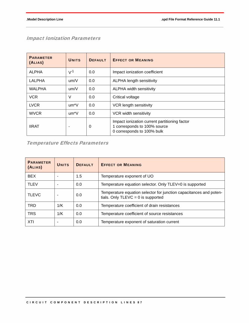
C I R C U I T C O M P O N E N T D E S C R I P T I O N L I N E S 8 7
.Model Description Line .spd File Format Reference Guide 11.1
Impact Ionization Parameters
Temperature Effects Parameters
PARAMETER (ALIAS) UNITS DEFAULT EFFECT OR MEANING
ALPHA V-1 0.0 Impact ionization coefficient
LALPHA um/V 0.0 ALPHA length sensitivity
WALPHA um/V 0.0 ALPHA width sensitivity
VCR V 0.0 Critical voltage
LVCR um*V 0.0 VCR length sensitivity
WVCR um*V 0.0 VCR width sensitivity
IIRAT - 0Impact ionization current partitioning factor1 corresponds to 100% source0 corresponds to 100% bulk
PARAMETER (ALIAS) UNITS DEFAULT EFFECT OR MEANING
BEX - 1.5 Temperature exponent of UO
TLEV - 0.0 Temperature equation selector. Only TLEV=0 is supported
TLEVC - 0.0 Temperature equation selector for junction capacitances and poten-tials. Only TLEVC = 0 is supported
TRD 1/K 0.0 Temperature coefficient of drain resistances
TRS 1/K 0.0 Temperature coefficient of source resistances
XTI - 0.0 Temperature exponent of saturation current
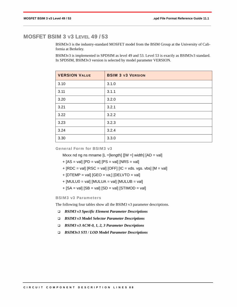
C I R C U I T C O M P O N E N T D E S C R I P T I O N L I N E S 8 8
MOSFET BSIM 3 v3 Level 49 / 53 .spd File Format Reference Guide 11.1
MOSFET BSIM 3 V3 LEVEL 49 / 53BSIM3v3 is the industry-standard MOSFET model from the BSIM Group at the University of Cali-fornia at Berkeley.
BSIM3v3 is implemented in SPDSIM as level 49 and 53. Level 53 is exactly as BSIM3v3 standard. In SPDSIM, BSIM3v3 version is selected by model parameter VERSION.
General Form for BSIM3 v3Mxxx nd ng ns mname [L =]length] [[W =] width] [AD = val]
+ [AS = val] [PD = val] [PS = val] [NRS = val]
+ [RDC = val] [RSC = val] [OFF] [IC = vds. vgs. vbs] [M = val]
+ [DTEMP = val] [GEO = va;] [DELVTO = val]
+ [MULU0 = val] [MULUA = val] [MULUB = val]
+ [SA = val] [SB = val] [SD = val] [STIMOD = val]
BSIM3 v3 ParametersThe following four tables show all the BSIM3 v3 parameter descriptions.
BSIM3 v3 Specific Element Parameter Descriptions
BSIM3 v3 Model Selector Parameter Descriptions
BSIM3 v3 ACM-0, 1, 2, 3 Parameter Descriptions
BSIM3v3 STI / LOD Model Parameter Descriptions
VERSION VALUE BSIM 3 V3 VERSION
3.10 3.1.0
3.11 3.1.1
3.20 3.2.0
3.21 3.2.1
3.22 3.2.2
3.23 3.2.3
3.24 3.2.4
3.30 3.3.0
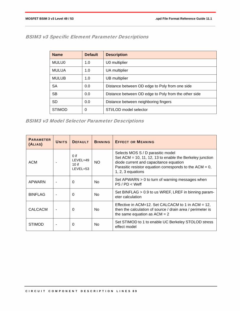
C I R C U I T C O M P O N E N T D E S C R I P T I O N L I N E S 8 9
MOSFET BSIM 3 v3 Level 49 / 53 .spd File Format Reference Guide 11.1
BSIM3 v3 Specific Element Parameter Descriptions
BSIM3 v3 Model Selector Parameter Descriptions
Name Default Description
MULU0 1.0 U0 multiplier
MULUA 1.0 UA multiplier
MULUB 1.0 UB multiplier
SA 0.0 Distance between OD edge to Poly from one side
SB 0.0 Distance between OD edge to Poly from the other side
SD 0.0 Distance between neighboring fingers
STIMOD 0 STI/LOD model selector
PARAMETER (ALIAS) UNITS DEFAULT BINNING EFFECT OR MEANING
ACM -
0 if LEVEL=4910 if LEVEL=53
NO
Selects MOS S / D parasitic modelSet ACM = 10, 11, 12, 13 to enable the Berkeley junction diode current and capacitance equation Parasitic resistor equation corresponds to the ACM = 0, 1, 2, 3 equations
APWARN - 0 No Set APWARN > 0 to turn of warning messages when PS / PD < Weff
BINFLAG - 0 No Set BINFLAG > 0.9 to us WREF, LREF in binning param-eter calculation
CALCACM - 0 NoEffective in ACM=12. Set CALCACM to 1 in ACM = 12, then the calculation of source / drain area / perimeter is the same equation as ACM = 2
STIMOD - 0 No Set STIMOD to 1 to enable UC Berkeley STOLOD stress effect model
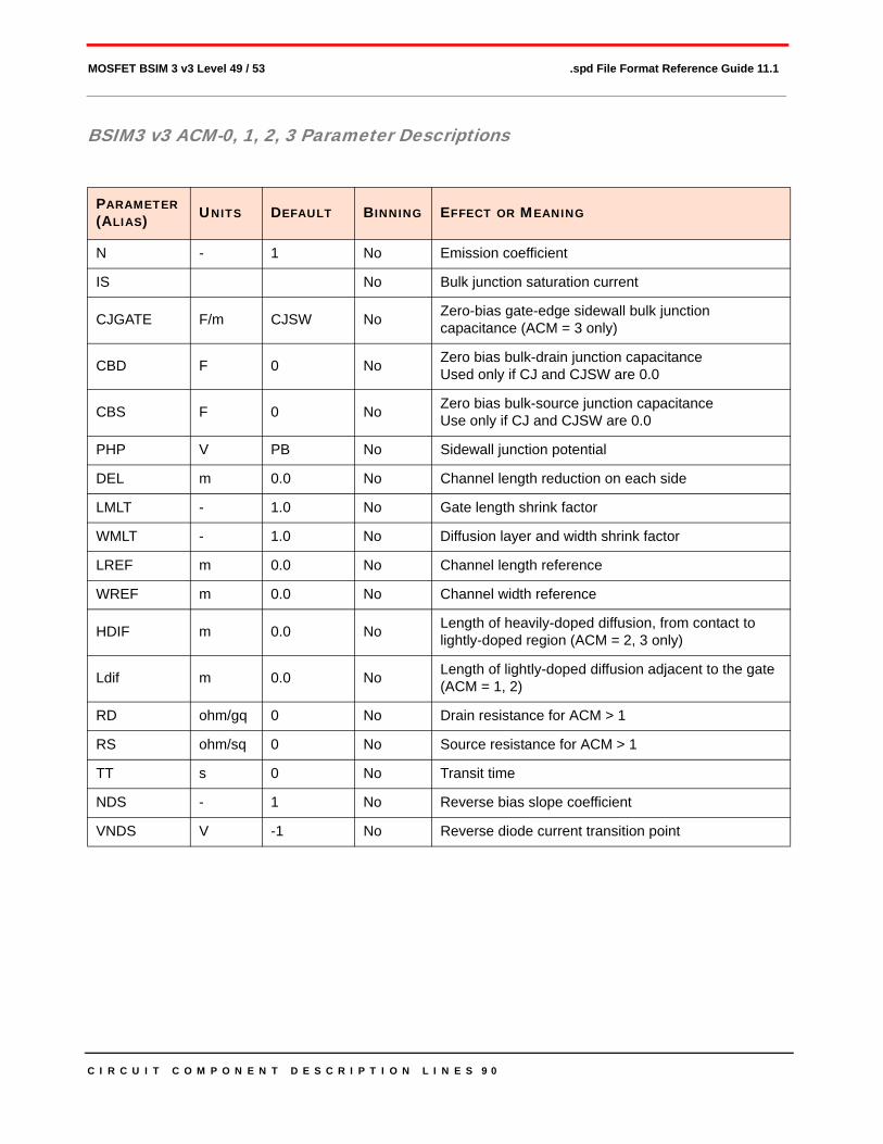
C I R C U I T C O M P O N E N T D E S C R I P T I O N L I N E S 9 0
MOSFET BSIM 3 v3 Level 49 / 53 .spd File Format Reference Guide 11.1
BSIM3 v3 ACM-0, 1, 2, 3 Parameter Descriptions
PARAMETER (ALIAS) UNITS DEFAULT BINNING EFFECT OR MEANING
N - 1 No Emission coefficient
IS No Bulk junction saturation current
CJGATE F/m CJSW No Zero-bias gate-edge sidewall bulk junction capacitance (ACM = 3 only)
CBD F 0 No Zero bias bulk-drain junction capacitance Used only if CJ and CJSW are 0.0
CBS F 0 No Zero bias bulk-source junction capacitance Use only if CJ and CJSW are 0.0
PHP V PB No Sidewall junction potential
DEL m 0.0 No Channel length reduction on each side
LMLT - 1.0 No Gate length shrink factor
WMLT - 1.0 No Diffusion layer and width shrink factor
LREF m 0.0 No Channel length reference
WREF m 0.0 No Channel width reference
HDIF m 0.0 No Length of heavily-doped diffusion, from contact to lightly-doped region (ACM = 2, 3 only)
Ldif m 0.0 No Length of lightly-doped diffusion adjacent to the gate (ACM = 1, 2)
RD ohm/gq 0 No Drain resistance for ACM > 1
RS ohm/sq 0 No Source resistance for ACM > 1
TT s 0 No Transit time
NDS - 1 No Reverse bias slope coefficient
VNDS V -1 No Reverse diode current transition point

C I R C U I T C O M P O N E N T D E S C R I P T I O N L I N E S 9 1
MOSFET BSIM 3 v3 Level 49 / 53 .spd File Format Reference Guide 11.1
BSIM3v3 STI / LOD Model Parameter Descriptions
PARAMETER (ALIAS) UNITS DEFAULT BINNING EFFECT OR MEANING
SAREF m 1.0e-6 NO Reference distance between OD and edge to poly of one side
SBREF m 1.0e-6 NO Reference distance between OD and edge to poly of the other side
WLOD m 0.0 NO Width parameter for stress effect
KU0 m 0.0 NO Mobility degradation / enhancement parameter for stress effect
KVSAT m 0.0 NO Saturation velocity degradation / enhancement parame-ter for stress effect
TKU0 m 0.0 No Temperature coefficient of KU0
LKU0 m 0.0 No Length dependence of KU0
PKU0 - 0.0 No Cross-term dependence of KU0
LLODKU0 - 0.0 No Length parameter for u0 stress effect
WLODKU0 - 0.0 No Width parameter for u0 stress effect
KVTH0 V 0.0 No Threshold shift parameter for stress effect
LKVTH0 - 0.0 No Length dependence of KVTH0
WKVTH0 - 0.0 No Width dependence of KVTH0
PKVTH0 - 0.0 No Cross-term dependence of KVTH0
LLODVTH - 0.0 No Length parameter for Vth stress effect
WLODVTH - 0.0 No Width parameter for Vth stress effect
STK2 m 0.0 No K2 shift factor related to Vth0 change
LODK2 - 1.0 No K2 shift modification factor for stress effect
STETA0 m 0.0 No Eta0 shift factor related to Vth0
LODETA0 - 1.0 No Eta0 shift modification factor for stress effect

C I R C U I T C O M P O N E N T D E S C R I P T I O N L I N E S 9 2
MOSFET BSIM4 Level 54 .spd File Format Reference Guide 11.1
MOSFET BSIM4 LEVEL 54BSIM4 is the latest industry-standard MOSFET model from the BSIM Group at the University of Cal-ifornia at Berkeley. BSIM4 is implemented in spdsim as level 54. Level 53 is exactly the same as BSIM3v3 standard.
In spdsim, BSIM4 version is selected by model parameter VERSION.
General FormMxxx nd ng ns nb mname [L=VAL] [W=VAL] [M=VAL]
+ [AD=VAL] [AS=VAL] [PD=VAL] [PS=VAL]
+ [NRS=VAL] [NRD=VAL] [DELVTO=VAL]
+ [RDC=VAL] [RSC=VAL] [DTEMP = va;]
+ [OFF] [IC=Vds, Vgs, Vbs]
+ [RGATEMOD=VAL] [RBODYMOD=VAL]
+ [GEOMOD=VAL] [RGEOMOD=VAL]
+ [NF=VAL] [RBPB=VAL] [RBPD=VAL]
+ [RBPS=VAL] [RBDB=VAL] [RBSB=VAL]
+ [MIN=VAL] [DELTOX=VAL]
+ [MULU0=VAL] [DELK1=VAL] [DELNFCT=VAL]
+ [SA=VAL] [SB=VAL] [SD=VAL] [STIMOD=VAL]
+ [SCA=VAL] [SCB=VAL] [SCC=VAL] [SC=VAL]
+ [XGW=VAL] [NGCON=VAL]
VERSION Value BSIM4 Version
4.00 4.0.0
4.10 4.1.0
4.20 4.2.0
4.21 4.2.1
4.30 4.3.0
4.40 4.4.0
4.50 4.5.0
4.60 4.6.0
4.61 4.6.1

C I R C U I T C O M P O N E N T D E S C R I P T I O N L I N E S 9 3
MOSFET BSIM4 Level 54 .spd File Format Reference Guide 11.1
BSIM4 Specific Element Parameter Descriptions
NAME DEFAULT DESCRIPTION
RGATEMOD 0 Gate resistance model selector
RBODYMOD 0 Substrate resistance network model selector
TRNQSMOD 0 Transient NQS model selector
GWOMOD 0 Geometry-dependent parasitics model selector
RGEOMOD 0 Source / drain diffusion resistance and contact model selector
RBPB 50ohm Resistance connected between bNodePrime and bNode
RBPD 50ohm Resistance connected between bNodePrime and dbNode
RBPS 50ohm Resistance connected between bNodePrime and sbNode
RBDB 50ohm Resistance connected between dbNode and bNode.
RBSB 50ohm Resistance connected between sbNode and bNode
NF 1 Number of fingers
MIN 0 Whether to minimize the number of drain or source diffusions for even-number fingered device
XGW 0m Distance from the gate contact to the channel edge
NGCON 1 Number of gate contacts
MULU0 1.0 U0 multiplier
DELK1 0.0 Shift in K1
DELNFCT 0.0 Shift in NFACTOR
DELTOX 0.0 Shift in TOXE and TOXP
STIMOD 0 STI / LOD model selector
SCA 0.0 Integral of the first distribution function for scattered well dopant
SCB 0.0 Integral of the second distribution function for scattered well dopant
SCC 0.0 Integral of the third distribution function for scattered well dopant
SC 0.0m Distance to a single well edge

C I R C U I T C O M P O N E N T D E S C R I P T I O N L I N E S 9 4
Subcircuit Command .spd File Format Reference Guide 11.1
Additional BSIM4 Model Parameters in SPDSIM
SUBCIRCUIT COMMANDIf a partial circuit contains subcircuits, none of the local variables that are defined in the partial circuit can be seen inside the subcircuit. the name of the subcircuit definition.
General Form .SUBCKT SubCKTName {ExtNodeName} [{ParameterX=valueX}]
General Form for .EndS.EndS SubCKTName
SUBCKT Example 1 .SUBCKT connector 1 2 gndC1 1 gnd 0.415pFL1 1 1a 2.4nR1 1a 2.4nC2 2 gnd 0.415pF.EndS
.SUBCKT IOBufferD nd_pu nd_pd nd_pin gnd nd_pc nd_gcB_io nd_pu nd_pd nd_pin dn_in nd_en gnd nd_out_in nd_pcnd_gc+ file=’t96b.ibs’ model=”DQ_FULL’+type=type+buffer=input_output+package=yesV_in nd_in gnd pulse (0V 2.5v 0n 0.5n 0.5n 1n 4n)V_en nd_en gnd 2.5v.EndS
PARAMETER (ALIAS) UNITS DEFAULT BINNING EFFECT OR MEANING
STIMOD -
Version < 4.30Version >= 4.301
NoSTI / LOD model selector Set STIMOD to 0 to disable STI / LOD model To Version > = 4.30, STIMOD is ignored.
TRS - 0.0 No Temperature coefficient of source resistance
TRD - 0.0 No Temperature coefficient of drain resistance
LMLT - 1.0 No Channel length multiplier
WMLT - 1.0 No Channel width multiplier

C I R C U I T C O M P O N E N T D E S C R I P T I O N L I N E S 9 5
Subcircuit Command .spd File Format Reference Guide 11.1
SUBCKT Example 2.SUBCKT Cap 1 2 3 rvalue=1 cvalue=1pR 1 2 rvalueC 2 3 cvalue.EndP
SUBCKT Example 3.SUBCKT Sub1 1 2R 1 2 rvalue.EndS
.PartialCKT Circuit rvalue=50X 3 4 sub1R1 3 4 rvalue.EndP
In Example 3, rvalue is defined in the partial circuit, Circuit.
It cannot be used by the subcircuit, Sub1; therefore, rvalue in Sub1 is an undefined parameter, unless it is defined globally within .Param lines.
SUBCKT Example 4.SUBCKT Cap 1 2 C0=3pC 1 2 C0.EndS
.PartialCkt DecapXcap 3 4 Cap C0=1p.EndPartialCktIn Example 4, C0=3p specifies the default for C0. When the subcircuit, Cap, is called in, the partial circuit, Decap, the capacitor, C=1p (not 3p),because C0=1p overwrites the default value.
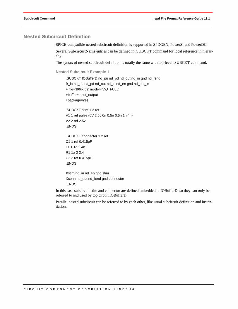
C I R C U I T C O M P O N E N T D E S C R I P T I O N L I N E S 9 6
Subcircuit Command .spd File Format Reference Guide 11.1
Nested Subcircuit DefinitionSPICE-compatible nested subcircuit definition is supported in SPDGEN, PowerSI and PowerDC.
Several SubcircuitName entries can be defined in .SUBCKT command for local reference in hierar-chy.
The syntax of nested subcircuit definition is totally the same with top-level .SUBCKT command.
Nested Subcircuit Example 1 .SUBCKT IOBufferD nd_pu nd_pd nd_out nd_in gnd nd_fend B_io nd_pu nd_pd nd_out nd_in nd_en gnd nd_out_in + file=’t96b.ibs’ model=”DQ_FULL’ +buffer=input_output +package=yes
.SUBCKT stim 1 2 ref V1 1 ref pulse (0V 2.5v 0n 0.5n 0.5n 1n 4n) V2 2 ref 2.5v .ENDS
.SUBCKT connector 1 2 ref C1 1 ref 0.415pF L1 1 1a 2.4n R1 1a 2 2.4 C2 2 ref 0.415pF .ENDS
Xstim nd_in nd_en gnd stim Xconn nd_out nd_fend gnd connector .ENDS
In this case subcircuit stim and connector are defined embedded in IOBufferD, so they can only be referred to and used by top circuit IOBufferD.
Parallel nested subcircuit can be referred to by each other, like usual subcircuit definition and instan-tiation.

C I R C U I T C O M P O N E N T D E S C R I P T I O N L I N E S 9 7
Subcircuit Command .spd File Format Reference Guide 11.1
Nested Subcircuit Example 2 .param trp=50p tfp=50p .param pw=1.4n per=3.0n .SUBCKT IOBufferD nd_pu nd_pd nd_out nd_in gnd nd_fend B_io nd_pu nd_pd nd_out nd_in nd_en gnd nd_out_in + file=’t96b.ibs’ model=”DQ_FULL’ +buffer=input_output +package=yes
.param vil=0 vih=2.5 .SUBCKT stim 1 2 ref .param dly=0 V1 1 ref pulse (vil vih dly trp tfp pw per) V2 2 ref vih .ENDS
.SUBCKT connector 1 2 ref C1 1 ref cload L1 1 1a 2.4n R1 1a 2 rs C2 2 ref cload .param rs=2.4 .ENDS
Xstim nd_in nd_en gnd stim Xconn nd_out nd_fend gnd connector .param cload=0.415pF .ENDS
Global defined parameters (trp, tfp, pw, per) and local defined parameters (vil, vih, dly, cload, rs ) can be referred to by circuit element definition in proper scope. Global and higher-level defined parameters can be referred to by lower-level circuit and elements.
For example, since parameter cload definition scope is the same with subcircuit connector, so it can be referred to by the capacitor element in connector definition.
Related Topic
• Broadband SPICE User’s Guide
NOTE!
1. Parameter definition in expression is NOT supported now. Following definition is regarded as invalid definition:
.param A = 'B/2-0.3' B=5.0n
2. Unable to define active element(B-element, Independent Voltage/Current source, and so on) in PowerSI extraction mode, and following error message will pop up:
Empty definition or unsupported circuit elements found for XXX

C I R C U I T C O M P O N E N T D E S C R I P T I O N L I N E S 9 8
Subcircuit Command .spd File Format Reference Guide 11.1
Subcircuit Parameter Definitions
GC - Capacitor Description Line
General FormCxxx n1 n2 [mname] [C = ] val|’expression’ [[TC1 = ]val]
+ [[TC2 = ] val ] [[SCALE = ] val ] [IC = val] [M = val] [W = val] [L = val]
+ [DTEMP = val]
C-Capacitor ExampleC31 21 22 0.047u
C32 1 2 value2 = ‘CAP’
In this example, CAP is a previously defined variable name equal to a constant value.
PARAMETER EFFECT OR MEANING
.SUBCKT .SUBCKT keyword
SubCKTName Character string for the name of the subcircuit definition
ExtNodeName Names of external nodes of the subcircuit
ParameterX=valueX
Local parameter specification. Affects only the partial circuit where it is defined; except any sub circuits (of the partial circuit) are not affected by the assignment.
A local parameter specification overrides a global parameter specification (made in the .param line)
If the same local parameter name is used more than once in a circuit definition, the latter value assignment is used
Where ParameterX is a character string for the name of the parameter, the = sign is required; value1 specifies the value of the parameter
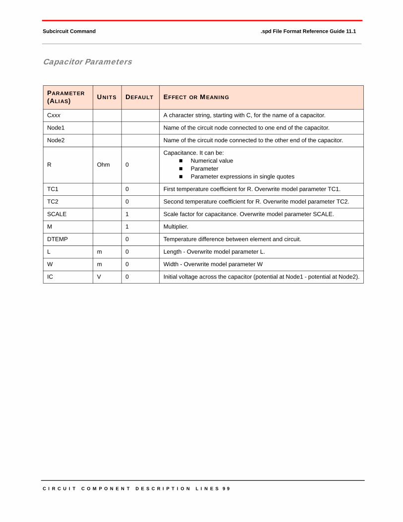
C I R C U I T C O M P O N E N T D E S C R I P T I O N L I N E S 9 9
Subcircuit Command .spd File Format Reference Guide 11.1
Capacitor Parameters
PARAMETER (ALIAS) UNITS DEFAULT EFFECT OR MEANING
Cxxx A character string, starting with C, for the name of a capacitor.
Node1 Name of the circuit node connected to one end of the capacitor.
Node2 Name of the circuit node connected to the other end of the capacitor.
R Ohm 0
Capacitance. It can be:Numerical valueParameterParameter expressions in single quotes
TC1 0 First temperature coefficient for R. Overwrite model parameter TC1.
TC2 0 Second temperature coefficient for R. Overwrite model parameter TC2.
SCALE 1 Scale factor for capacitance. Overwrite model parameter SCALE.
M 1 Multiplier.
DTEMP 0 Temperature difference between element and circuit.
L m 0 Length - Overwrite model parameter L.
W m 0 Width - Overwrite model parameter W
IC V 0 Initial voltage across the capacitor (potential at Node1 - potential at Node2).

C I R C U I T C O M P O N E N T D E S C R I P T I O N L I N E S 1 0 0
Subcircuit Command .spd File Format Reference Guide 11.1
_Cmatrix - Mutual Capacitor Matrix Description Line
General Form_Cmatrixxxxx N = n1 file = s1 Node0 Node1 … NodeN
Mutual Capacitor Matrix Parameter Descriptions
D - Diode Description Line
General FormDxxx Node1 Node2 ModelName [[AREA = ]val] [[PJ = ]val
+ [WP = val] [LP = val] [WP = val] [LM = val] [OFF]
+ [IC = vd] [M = val] pDTEMP = val]
or
Dxxx Node1 Node2 ModelName [W = width] [L = length]
+ [WP = val] [LP = val] [WM = val] [LM = val] [OFF]
+ [IC = vd] [M = val] [DTEMP = val]
D-Diode Exampled1 1 2 diode1
PARAMETER EFFECT OR MEANING
_Cmatrixxxxx A character string, starting with _Cmatrix, for the name of a mutual capacitor matrix.
N = n1 Number of nodes involved, other than the reference node.
file = s1 Character string for the name of the data file in disk that stores the mutual capacitance values.
Node0 Name of the reference node in the mutual capacitor matrix.
Node 1 to NodeN Names of N nodes, other than the reference node, of the mutual capacitor matrix.
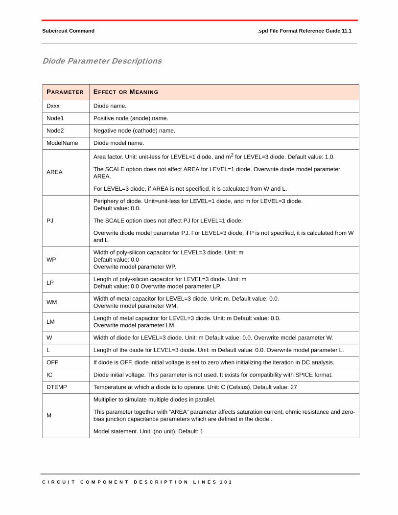
C I R C U I T C O M P O N E N T D E S C R I P T I O N L I N E S 1 0 1
Subcircuit Command .spd File Format Reference Guide 11.1
Diode Parameter Descriptions
PARAMETER EFFECT OR MEANING
Dxxx Diode name.
Node1 Positive node (anode) name.
Node2 Negative node (cathode) name.
ModelName Diode model name.
AREA
Area factor. Unit: unit-less for LEVEL=1 diode, and m2 for LEVEL=3 diode. Default value: 1.0.
The SCALE option does not affect AREA for LEVEL=1 diode. Overwrite diode model parameter AREA.
For LEVEL=3 diode, if AREA is not specified, it is calculated from W and L.
PJ
Periphery of diode. Unit=unit-less for LEVEL=1 diode, and m for LEVEL=3 diode. Default value: 0.0.
The SCALE option does not affect PJ for LEVEL=1 diode.
Overwrite diode model parameter PJ. For LEVEL=3 diode, if P is not specified, it is calculated from W and L.
WPWidth of poly-silicon capacitor for LEVEL=3 diode. Unit: m Default value: 0.0 Overwrite model parameter WP.
LP Length of poly-silicon capacitor for LEVEL=3 diode. Unit: m Default value: 0.0 Overwrite model parameter LP.
WM Width of metal capacitor for LEVEL=3 diode. Unit: m. Default value: 0.0. Overwrite model parameter WM.
LM Length of metal capacitor for LEVEL=3 diode. Unit: m Default value: 0.0. Overwrite model parameter LM.
W Width of diode for LEVEL=3 diode. Unit: m Default value: 0.0. Overwrite model parameter W.
L Length of the diode for LEVEL=3 diode. Unit: m Default value: 0.0. Overwrite model parameter L.
OFF If diode is OFF, diode initial voltage is set to zero when initializing the iteration in DC analysis.
IC Diode initial voltage. This parameter is not used. It exists for compatibility with SPICE format.
DTEMP Temperature at which a diode is to operate. Unit: C (Celsius). Default value: 27
M
Multiplier to simulate multiple diodes in parallel.
This parameter together with “AREA” parameter affects saturation current, ohmic resistance and zero-bias junction capacitance parameters which are defined in the diode .
Model statement. Unit: (no unit). Default: 1
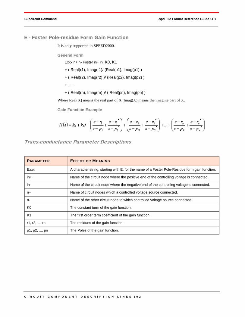
C I R C U I T C O M P O N E N T D E S C R I P T I O N L I N E S 1 0 2
Subcircuit Command .spd File Format Reference Guide 11.1
E - Foster Pole-residue Form Gain FunctionIt is only supported in SPEED2000.
General FormExxx n+ n- Foster in+ in K0, K1
+ ( Real(r1), Imag(r1)/ (Real(p1), Imag(p1) )
+ ( Real(r2), Imag(r2) )/ (Real(p2), Imag(p2) )
+ .....
+ ( Real(rn), Imag(rn) )/ ( Real(pn), Imag(pn) )
Where Real(X) means the real part of X, Imag(X) means the imagine part of X.
Gain Function Example
Trans-conductance Parameter Descriptions
PARAMETER EFFECT OR MEANING
Exxx A character string, starting with E, for the name of a Foster Pole-Residue form gain function.
in+ Name of the circuit node where the positive end of the controlling voltage is connected.
in- Name of the circuit node where the negative end of the controlling voltage is connected.
n+ Name of circuit nodes which a controlled voltage source connected.
n- Name of the other circuit node to which controlled voltage source connected.
K0 The constant term of the gain function.
K1 The first order term coefficient of the gain function.
r1, r2, ..., rn The residues of the gain function.
p1, p2, ..., pn The Poles of the gain function.

C I R C U I T C O M P O N E N T D E S C R I P T I O N L I N E S 1 0 3
Subcircuit Command .spd File Format Reference Guide 11.1
E - Laplace and Pole-zero Voltage Gain FunctionThere are two general forms: Laplace and Pole. They are only supported in SPEED2000.
General Form for LaplaceExxx n+ n- LAPLACE in+ in k0, k1, ..., kn / d0, d1, ..., dm
General Form for PoleExxx n+ n- POLE in+ in a az1, fz1, ..., azn, fzn / b , ap1, fp1, ..., apn , fpn
Using the Parameters-kn — Should not be all zero
-dm — Should not be all zero
-azn , fzn — Should be all non-negative
-apn , fpn — Should be all non-negative
-a, b — Should not be zero
Parameters Example 1
Parameters Example 2
Voltage Gain Parameter Descriptions
PARAMETER EFFECT OR MEANING
Exxx A character string for name of Laplace or Pole-zero voltage gain function.
in+ Circuit node where positive end of controlling voltage connected.
in- Circuit node where negative end of controlling voltage connected.
n+ Name of circuit nodes where a controlled current source connected.
n- Name of other circuit node to which controlled current source connected.
k0, k1, ..., kn d0, d1, ..., dm The corresponding parameters in a voltage gain function.
a az1, fz1, ..., azn , fzn b ap1, fp1 , ..., apn, fpn The corresponding parameters in a voltage gain function.
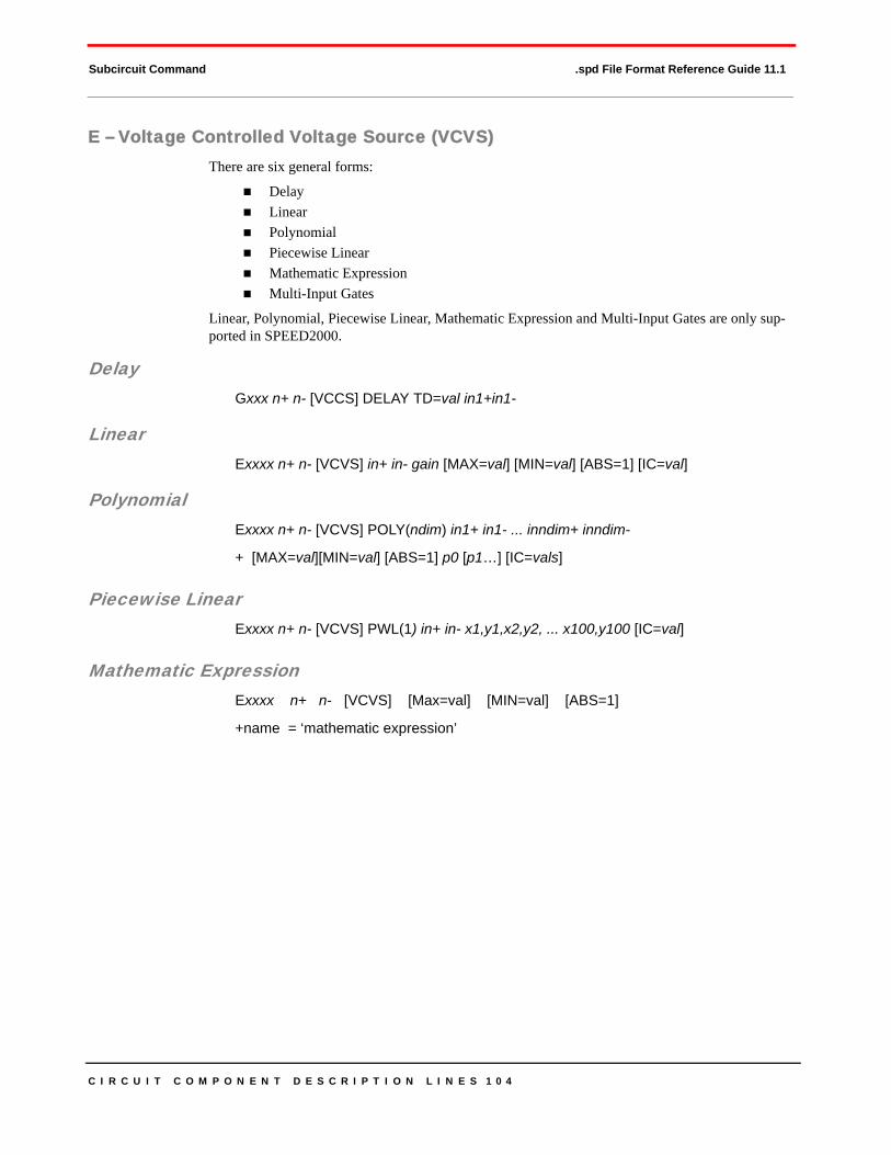
C I R C U I T C O M P O N E N T D E S C R I P T I O N L I N E S 1 0 4
Subcircuit Command .spd File Format Reference Guide 11.1
E – Voltage Controlled Voltage Source (VCVS)There are six general forms:
DelayLinearPolynomialPiecewise LinearMathematic ExpressionMulti-Input Gates
Linear, Polynomial, Piecewise Linear, Mathematic Expression and Multi-Input Gates are only sup-ported in SPEED2000.
DelayGxxx n+ n- [VCCS] DELAY TD=val in1+in1-
LinearExxxx n+ n- [VCVS] in+ in- gain [MAX=val] [MIN=val] [ABS=1] [IC=val]
PolynomialExxxx n+ n- [VCVS] POLY(ndim) in1+ in1- ... inndim+ inndim-
+ [MAX=val][MIN=val] [ABS=1] p0 [p1…] [IC=vals]
Piecewise LinearExxxx n+ n- [VCVS] PWL(1) in+ in- x1,y1,x2,y2, ... x100,y100 [IC=val]
Mathematic ExpressionExxxx n+ n- [VCVS] [Max=val] [MIN=val] [ABS=1]
+name = ‘mathematic expression’

C I R C U I T C O M P O N E N T D E S C R I P T I O N L I N E S 1 0 5
Subcircuit Command .spd File Format Reference Guide 11.1
Multi-Input GatesGxxx n+ n- [VCCS] gatetype(ndim) in1+in1- inndim+inndim-
+ [M=val] [ABS=1] x1,y1 ... x1000,y100[IC=val]
TransformerExxx n+ n- TRANSFORMER in+ in- k
Related Topics
• Transient Waveform Specifications
• Arbitrary Mathematical Expression Processing
Voltage Controlled Voltage Parameter Descriptions
PARAMETER EFFECT OR MEANING
Exxxx Character string, starting with E, for the name of a voltage controlled source.
ABS=1 Output is absolute value if ABS=1.
DELAY Delay Key function.
gain Voltage gain. The ratio between the controlled voltage and the controlling voltage.
gatetype Multi-Input Gates Key function. Can be AND, NAND, OR, NOR.
IC=val Initial condition. The initial estimate of the value(s) of the controlling voltage(s). If IC is not specified, the default=0.0. For IC=vals there can be up to three values.
in+ Name of circuit node to which the positive end of the controlling voltage is connected.
in- Name of circuit node to which the negative end of the controlling voltage is connected.
in1+, …, inndim+ Names of the circuit nodes to which positive ends of the controlling voltages are con-nected.
in1-, …, inndim- Names of circuit nodes to which negative ends of the controlling voltages are con-nected.
k Ideal transformer turn ratio: V(n+,n-)=k* V(in+,in-) or number of gates input.
gain = V /V+n , n- +in , in-
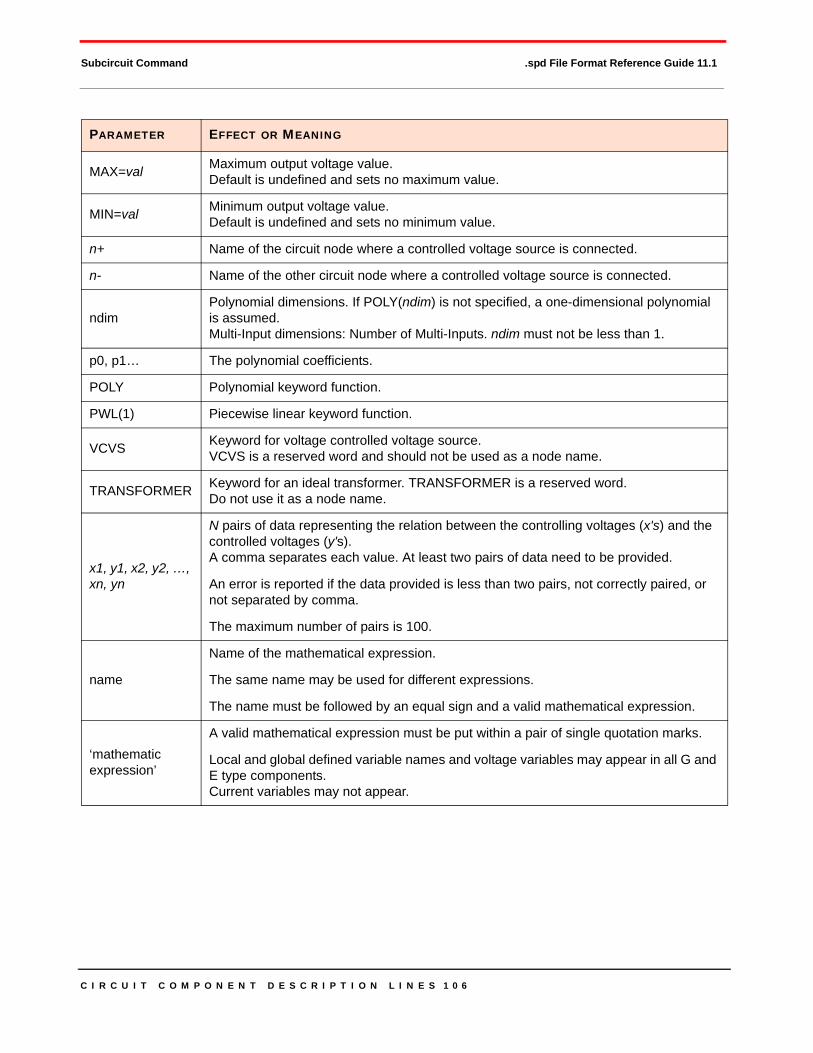
C I R C U I T C O M P O N E N T D E S C R I P T I O N L I N E S 1 0 6
Subcircuit Command .spd File Format Reference Guide 11.1
MAX=val Maximum output voltage value.Default is undefined and sets no maximum value.
MIN=val Minimum output voltage value.Default is undefined and sets no minimum value.
n+ Name of the circuit node where a controlled voltage source is connected.
n- Name of the other circuit node where a controlled voltage source is connected.
ndim Polynomial dimensions. If POLY(ndim) is not specified, a one-dimensional polynomial is assumed.Multi-Input dimensions: Number of Multi-Inputs. ndim must not be less than 1.
p0, p1… The polynomial coefficients.
POLY Polynomial keyword function.
PWL(1) Piecewise linear keyword function.
VCVS Keyword for voltage controlled voltage source. VCVS is a reserved word and should not be used as a node name.
TRANSFORMER Keyword for an ideal transformer. TRANSFORMER is a reserved word. Do not use it as a node name.
x1, y1, x2, y2, …, xn, yn
N pairs of data representing the relation between the controlling voltages (x's) and the controlled voltages (y's). A comma separates each value. At least two pairs of data need to be provided.
An error is reported if the data provided is less than two pairs, not correctly paired, or not separated by comma.
The maximum number of pairs is 100.
name
Name of the mathematical expression.
The same name may be used for different expressions.
The name must be followed by an equal sign and a valid mathematical expression.
‘mathematic expression’
A valid mathematical expression must be put within a pair of single quotation marks.
Local and global defined variable names and voltage variables may appear in all G and E type components. Current variables may not appear.
PARAMETER EFFECT OR MEANING
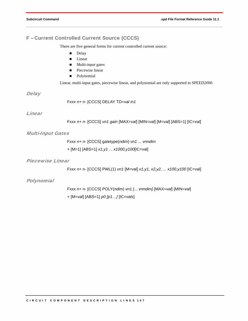
C I R C U I T C O M P O N E N T D E S C R I P T I O N L I N E S 1 0 7
Subcircuit Command .spd File Format Reference Guide 11.1
F – Current Controlled Current Source (CCCS)There are five general forms for current controlled current source:
DelayLinearMulti-input gatesPiecewise linearPolynomial
Linear, multi-input gates, piecewise linear, and polynomial are only supported in SPEED2000.
DelayFxxx n+ n- [CCCS] DELAY TD=val in1
LinearFxxx n+ n- [CCCS] vn1 gain [MAX=val] [MIN=val] [M=val] [ABS=1] [IC=val]
Multi-Input GatesFxxx n+ n- [CCCS] gatetype(ndim) vn1 ... vnndim
+ [M=1] [ABS=1] x1,y1 ... x1000,y100[IC=val]
Piecewise LinearFxxx n+ n- [CCCS] PWL(1) vn1 [M=val] x1,y1, x2,y2, ... x100,y100 [IC=val]
PolynomialFxxx n+ n- [CCCS] POLY(ndim) vn1 [... vnndim] [MAX=val] [MIN=val]
+ [M=val] [ABS=1] p0 [p1…] [IC=vals]

C I R C U I T C O M P O N E N T D E S C R I P T I O N L I N E S 1 0 8
Subcircuit Command .spd File Format Reference Guide 11.1
CCCS Parameter Descriptions
PARAMETER EFFECT OR MEANING
Fxxx A character string, starting with F, for the name of the current controlled current source.
ABS=1 Output is absolute value if ABS=1.
CCCS Keyword for a current controlled current source.
DELAY Delay Key function.
gain Current gain. For example, the ratio of the controlled current and the controlling current.
gatetype Multi-Input Gates Key function. Can be AND, NAND, OR, NOR.
IC=val Initial condition. The initial estimate of the values of the controlling currents in amps. If IC is not specified, the default=0.0. For IC=vals there can be up to three values.
M=val Number of elements in parallel.
MAX=val Maximum output current value. Default is undefined and sets no maximum value.
MIN=val Minimum output current value. Default is undefined and sets no minimum value.
n+ Name of the circuit node where a controlled current source is connected.
n- Name of the other circuit node where a controlled current source is connected.
ndim Polynomial dimensions or Multi-Input dimensions.Polynomial dimensions. If POLY(ndim) is not specified, a one-dimensional polynomial is assumed. Number of Multi-Inputs. ndim not less than 1.
p0, p1 … Polynomial coefficients.
POLY Polynomial keyword function.
PWL(1) Piecewise linear keyword function.
TD Propagation delay time.
vn1 … Names of voltage sources through which the controlling current flows. One name must be specified for each dimension. Other types of circuit elements are NOT valid.
vnndim Names of voltage sources through which the controlling current flows. One name must be specified for each dimension. Other types of circuit elements are NOT valid.
x1, y1, x2, y2, …, xn, yn
N pairs of data representing the relation between the controlling currents (x's) and the controlled currents (y's). A comma separates each value. At least two pairs of data need to be provided. An error is reported if the data provided is less than two pairs, not correctly paired, or not sepa-rated by comma. Maximum number of pairs = 100.
gain = I / I+n , n- +in , in-

C I R C U I T C O M P O N E N T D E S C R I P T I O N L I N E S 1 0 9
Subcircuit Command .spd File Format Reference Guide 11.1
G - Foster Pole-residue Form Trans-conductance FunctionThis function is only supported in SPEED2000.
General FormGxxx n+ n- Foster in+ in K0, K1
+ ( Real(r1), Imag(r1)/ ( Real(p1), Imag(p1) )
+ ( Real(r2), Imag(r2) )/ ( Real(p2), Imag(p2) )
+ .....
+ ( Real(rn), Imag(rn) )/ ( Real(pn), Imag(pn) )
Where Real(X) means the real part of X, Imag(X) means the imagine part of X.
Trans-conductance Function Example
Trans-conductance Parameter Descriptions
PARAMETER EFFECT OR MEANING
Gxxx A character string, starting with G, for the name of a Foster Pole-Residue form Trans-con-ductance function.
in+ Name of the circuit node where positive end of the controlling voltage is connected.
in- Name of the circuit node where the negative end of the controlling voltage is connected.
n+ Name of circuit nodes where a controlled current source is connected. By convention, cur-rent flows from n+ through the source to n-.
n- Name of the other circuit node to which controlled current source is connected.
K0 The constant term of the Trans-conductance function.
K1 The first order term coefficient of the Trans-conductance function.
r1, r2, ..., rn The residues of the Trans-conductance function.
p1, p2, ..., pn The Poles of the Trans-conductance function.

C I R C U I T C O M P O N E N T D E S C R I P T I O N L I N E S 1 1 0
Subcircuit Command .spd File Format Reference Guide 11.1
G - Laplace and Pole-zero Trans-conductance FunctionThere are two forms: Laplace and Pole. They are only supported in SPEED2000.
LaplaceGxxx n+ n- LAPLACE in+ in k0, k1, ..., kn / d0, d1, ..., dm
PoleGxxx n+ n- POLE in+ in a az1, fz1, ..., azn, fzn / b , ap1, fp1, ..., apn , fpn
Using the Trans-conductance Parameters-kn — Should not be all zero
-dm — Should not be all zero
-azn , fzn — Should be all non-negative
-apn , fpn — Should be all non-negative
-a, b — Should not be zero
Trans-conductance Example 1
Trans-conductance Example 2

C I R C U I T C O M P O N E N T D E S C R I P T I O N L I N E S 1 1 1
Subcircuit Command .spd File Format Reference Guide 11.1
Trans-conductance Parameter Descriptions
PARAMETER EFFECT OR MEANING
Gxxx A character string, starting with E, for the name of a Laplace or Pole-zero trans-conduc-tance function.
in+ Name of the circuit node where the positive end of the controlling voltage is connected.
in- Name of the circuit node where the negative end of the controlling voltage is connected.
n+ Name of the circuit nodes where a controlled current source is connected. By convention, current flows from n+ through the source to n-.
n- Name of the other circuit node to which controlled current source is connected.
k0, k1, ..., knd0, d1, ..., dm
The corresponding parameters in a trans-conductance function.
aaz1, fz1, ..., azn , fzn bap1, fp1 , ..., apn , fpn
The corresponding parameters in a trans-conductance function.

C I R C U I T C O M P O N E N T D E S C R I P T I O N L I N E S 1 1 2
Subcircuit Command .spd File Format Reference Guide 11.1
G – Voltage Controlled Capacitor (VCCAP)There are four general forms for VCCAP:
LinearMathematic expressionPiecewise linearPolynomial
They are only supported in SPEED2000.
LinearGxxx n+ n- VCCAP in+ in- transfactor [MAX=val] [MIN=val] [M=val] [IC=val]
Mathematic ExpressionGxxxx n+ n- VCCAP [Max=val] [MIN=val] [M=val]
+ name = ‘mathematic expression’
Piecewise LinearGxxx n+ n- VCCAP PWL(1) in+ in- [M=val] x1,y1,x2,y2 ... x100,y100 [IC=val]
PolynomialGxxx n+ n- VCCAP POLY(ndim) in1+ in1- ... [inndim+ inndim-] [MAX=val]
+ [MIN=val] [M=val] p0 [p1…] [IC=vals]
VCCAP ExampleG 1 0 VCCAP PWL(1) cp 0
+ 1 , 10p
+ 2, 50p
Related Topic
• Arbitrary Mathematical Expression Processing

C I R C U I T C O M P O N E N T D E S C R I P T I O N L I N E S 1 1 3
Subcircuit Command .spd File Format Reference Guide 11.1
VCCAP Parameter Descriptions
PARAMETER EFFECT OR MEANING
Gxxx A character string, starting with G, for the name of a Voltage Controlled Capacitor.
IC=val Initial estimate of the value of the controlling voltage. If IC is not specified, default = 0.0. For IC=vals there can be up to three values.
in+ Name of the circuit node where the positive end of the controlling voltage is connected.
in1+, …, inndim+ Names of the circuit nodes where positive ends of controlling voltages are connected.
in- Name of the circuit node where the negative end of the controlling voltage is con-nected.
in1-, …, inndim- Names of the circuit nodes where negative ends of controlling voltages are connected.
M=val Number of elements in parallel.
MAX=val Maximum capacitance value. Default is undefined and sets no maximum value.
MIN=val Minimum capacitance value. Default is undefined and sets no minimum value.
n+ Name of the circuit node where a controlled capacitor is connected.
n- Name of the other circuit node where a controlled capacitor is connected.
ndim Polynomial dimensions. Choices are 1, 2 and 3. If POLY(ndim) is not specified, a one-dimensional polynomial is assumed.
p0, p1... The polynomial coefficients.
POLY Polynomial keyword function.
PWL(1) Required key word for Piecewise Linear format. Error is reported if it is missing or incorrectly spelled.
transfactor Voltage-to-capacitance conversion factor. It equals to the ratio of the controlled capac-itor capacitance and the controlling voltage.
VCCAP Required key word to identify the type of Voltage Controlled Capacitor. An error is reported if it is missing or incorrectly spelled.
x1, y1, x2, y2, ..., xn, yn
N pairs of data representing the relation between Voltage (x's) and Capacitance (y's). A comma separates each value. At least two pairs of data need to be provided. An error is reported if the data provided is less than two pairs, not correctly paired, or not separated by comma. Maximum number of pairs = 100.
name Name of the mathematical expression. Same name may be used for different expres-sions. Name must be followed by an equal sign and a valid mathematical expression.
‘mathematic expression’
Valid mathematical expression must be put within a pair of single quotation marks. Local and global defined variable names and voltage variables may appear in all G and E type components mathematical expressions. Current variables may not appear.

C I R C U I T C O M P O N E N T D E S C R I P T I O N L I N E S 1 1 4
Subcircuit Command .spd File Format Reference Guide 11.1
G – Voltage Controlled Current Source (VCCS) There are six general forms for VCCS:
LinearDelayMathematic expressionMulti-input gatesPiecewise linearPolynomial
Delay, mathematic expression, multi-input gates, piecewise linear, and polynomial are only supported in SPEED2000.
LinearGxxx n+ n- [VCCS] in+ in- transconductance [MAX=val] [MIN=val]
+ [M=val] [IC=val]
DelayGxxx n+ n- [VCCS] DELAY TD=val in1+in1-
Mathematic ExpressionGxxxx n+ n- [VCCS] [Max=val] [MIN=val] [ABS=1] [M=val]
+ name = ‘mathematic expression’
Multi-Input GatesGxxx n+ n- [VCCS] gatetype(ndim) in1+in1- inndim+inndim-
+ [M=val] [ABS=1] x1,y1 ... x1000,y100[IC=val]
Piecewise LinearGxxx n+ n- [VCCS] PWL(1) in+ in- [M=val] x1,y1,x2,y2, ... x100,y100 [IC=val]
PolynomialGxxx n+ n- [VCCS] POLY (ndim ) in1+ in1- ... [inndim+ inndim-] [MAX=val]
+ [MIN=val] [M=val] p0 [p1…] [IC=vals]
Related Topics
• Arbitrary Mathematical Expression Processing
• Transient Waveform Specifications
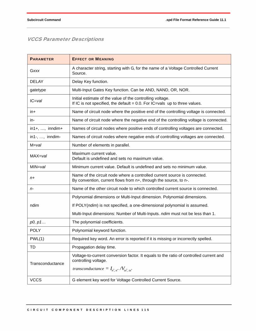
C I R C U I T C O M P O N E N T D E S C R I P T I O N L I N E S 1 1 5
Subcircuit Command .spd File Format Reference Guide 11.1
VCCS Parameter Descriptions
PARAMETER EFFECT OR MEANING
Gxxx A character string, starting with G, for the name of a Voltage Controlled Current Source.
DELAY Delay Key function.
gatetype Multi-Input Gates Key function. Can be AND, NAND, OR, NOR.
IC=val Initial estimate of the value of the controlling voltage. If IC is not specified, the default = 0.0. For IC=vals up to three values.
in+ Name of circuit node where the positive end of the controlling voltage is connected.
in- Name of circuit node where the negative end of the controlling voltage is connected.
in1+, …, inndim+ Names of circuit nodes where positive ends of controlling voltages are connected.
in1-, …, inndim- Names of circuit nodes where negative ends of controlling voltages are connected.
M=val Number of elements in parallel.
MAX=val Maximum current value.Default is undefined and sets no maximum value.
MIN=val Minimum current value. Default is undefined and sets no minimum value.
n+ Name of the circuit node where a controlled current source is connected. By convention, current flows from n+, through the source, to n-.
n- Name of the other circuit node to which controlled current source is connected.
ndim
Polynomial dimensions or Multi-Input dimension. Polynomial dimensions.
If POLY(ndim) is not specified, a one-dimensional polynomial is assumed.
Multi-Input dimensions: Number of Multi-Inputs. ndim must not be less than 1.
p0, p1… The polynomial coefficients.
POLY Polynomial keyword function.
PWL(1) Required key word. An error is reported if it is missing or incorrectly spelled.
TD Propagation delay time.
Transconductance
Voltage-to-current conversion factor. It equals to the ratio of controlled current and controlling voltage.
VCCS G element key word for Voltage Controlled Current Source.
transconductance = I /V+n , n- +in , in-

C I R C U I T C O M P O N E N T D E S C R I P T I O N L I N E S 1 1 6
Subcircuit Command .spd File Format Reference Guide 11.1
Mathematical ExpressionsThe controlling voltages denote voltage variables of the first form. A voltage variable of the first form expresses the voltage difference between two circuit nodes.
General FormsGy ref y1 CUR=' deltai * ( V(w1, gnd) * V(f1, gnd) + V(w2, gnd) * V(f2, gnd) ) '
“deltai” is a previously defined variable name
“ref” is the positive node of the G component
“y1” is the negative node of the G component
VCCS “Gy” is controlled by four controlling voltages:
V(w1, gnd)V(f1, gnd)V(w2, gnd)V(f2, gnd)
Related Topic
• Arbitrary Mathematical Expression Processing
x1, y1, x2, y2, …, xn, yn
N pairs of data representing the relation between the controlling voltages (x's) and the controlled currents (y's).
A comma separates each value.
At least two pairs of data need to be provided.
An error is reported if the data provided is less than two pairs, not correctly paired, or not separated by comma. Max number of pairs is 100.
name Name of the mathematical expression.Same name may be used for different expressions.
Name must be followed by an equal sign and a valid mathematical expression.
‘mathematic expression’
A valid mathematical expression must be put within a pair of single quotation marks.
Local and global defined variable names and voltage variables may appear in all G and E type components.
Current variables may not appear.
PARAMETER EFFECT OR MEANING
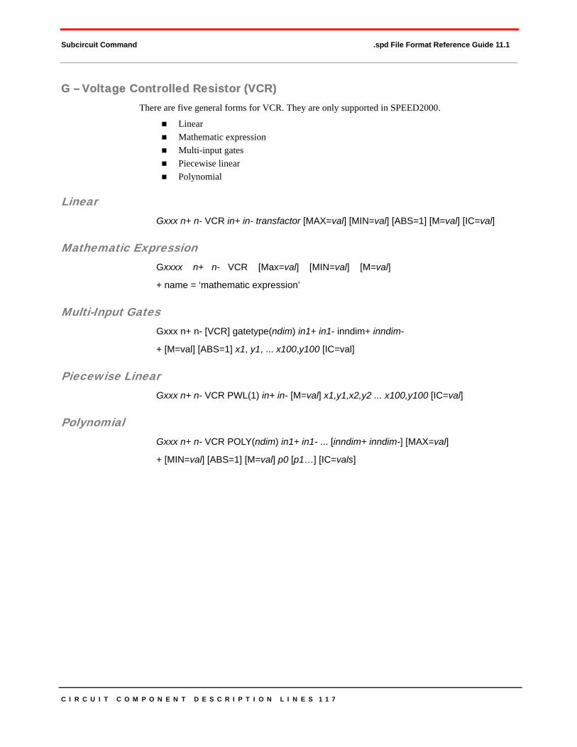
C I R C U I T C O M P O N E N T D E S C R I P T I O N L I N E S 1 1 7
Subcircuit Command .spd File Format Reference Guide 11.1
G – Voltage Controlled Resistor (VCR)There are five general forms for VCR. They are only supported in SPEED2000.
LinearMathematic expressionMulti-input gatesPiecewise linearPolynomial
Linear Gxxx n+ n- VCR in+ in- transfactor [MAX=val] [MIN=val] [ABS=1] [M=val] [IC=val]
Mathematic ExpressionGxxxx n+ n- VCR [Max=val] [MIN=val] [M=val]
+ name = ‘mathematic expression’
Multi-Input GatesGxxx n+ n- [VCR] gatetype(ndim) in1+ in1- inndim+ inndim-
+ [M=val] [ABS=1] x1, y1, ... x100,y100 [IC=val]
Piecewise LinearGxxx n+ n- VCR PWL(1) in+ in- [M=val] x1,y1,x2,y2 ... x100,y100 [IC=val]
PolynomialGxxx n+ n- VCR POLY(ndim) in1+ in1- ... [inndim+ inndim-] [MAX=val]
+ [MIN=val] [ABS=1] [M=val] p0 [p1…] [IC=vals]

C I R C U I T C O M P O N E N T D E S C R I P T I O N L I N E S 1 1 8
Subcircuit Command .spd File Format Reference Guide 11.1
VCR Parameter Descriptions
PARAMETER EFFECT OR MEANING
Gxxx A character string, starting with G, for the name of a Voltage Controlled Resistor.
DELAY Delay Key function.
gatetype Multi-Input Gates Key function. Can be AND, NAND, OR, NOR.
IC=val Initial estimate of the value of the controlling voltage. If IC is not specified, the default = 0.0. For IC=vals there can be up to three values.
in+ Name of circuit node where the positive end of the controlling voltage is connected.
in1+, …, inndim+ Names of circuit nodes where positive ends of controlling voltages are connected.
in- Name of circuit node where the negative end of the controlling voltage is connected.
in1-, …, inndim- Names of circuit nodes where negative ends of controlling voltages are connected.
M=val Number of elements in parallel.
MAX=val Maximum resistance value. Default is undefined and sets no maximum value.
MIN=val Minimum resistance value. Default is undefined and sets no minimum value.
n+ Name of the circuit node where a controlled resistor is connected.
n- Name of the other circuit node where a controlled resistor is connected.
ndim
Polynomial dimensions or Multi-Inpt dimension.
If POLY(ndim) is not specified, a one-dimensional polynomial is assumed.
Multi-Input dimension: Number of Multi-Inputs. ndim must not be less than 1.
p0, p1… The polynomial coefficients.
POLY Polynomial keyword function.
PWL(1) Required key word for Piecewise Linear format. Error is reported if it is missing or incorrectly spelled.
TD Propagation delay time.
transfactorVoltage-to-resistance conversion factor. It equals to the ratio of the controlled resistor
and the controlling voltage.
VCR Required key word to identify the type of Voltage Controlled Resistor. Error is reported if it is missing or incorrectly spelled.
transfactor = R /V+n , n- +in , in-

C I R C U I T C O M P O N E N T D E S C R I P T I O N L I N E S 1 1 9
Subcircuit Command .spd File Format Reference Guide 11.1
H – Current Controlled Voltage Source (CCVS)There are five general forms for current controlled voltage source: linear, delay, multi-input gates, piecewise linear, and polynomial.
Delay, multi-input gates, piecewise linear, and polynomial are only supported in SPEED2000.
LinearHxxx n+ n- [CCVS] vn1 transresistance [MAX=val] [MIN=val] [ABS=1] [IC=val]
Delay Hxxx n+ n- [CCVS] DELAY TD=val in1
Multi-Input GatesHxxx n+ n- [CCVS] gatetype(ndim) vn1, ... vnndim
+ [ABS=1] x1,y1 ... x1000,y100[IC=val]
Piecewise LinearHxxx n+ n- [CCVS] PWL(1) vn1 x1,y1,x2,y2, ... x100,y100 [IC=val]
PolynomialHxxx n+ n- [CCVS] POLY(ndim) vn1 [... vnndim] [MAX=val] [MIN=val]
+ [ABS=1] p0 [p1…] [IC=vals]
Related Topic
• Transient Waveform Specifications
x1, y1, x2, y2, …, xn, yn
N pairs of data representing the relation between Voltage (x's) and Resistance (y's).
A comma separates each value. At least two pairs of data need to be provided.
Error is reported if the data provided is less than two pairs, not correctly paired, or not separated by comma. Maximum number of pairs is 100.
name Name of mathematical expression. Same name may be used for different expres-sions.
Name must be followed by an equal sign and a valid mathematical expression.
‘mathematic expression’
Valid mathematical expression must be put within a pair of single quotation marks.
Local and global defined variable names and voltage variables may appear in all G and E type components mathematical expressions.
Current variables may not appear.
PARAMETER EFFECT OR MEANING

C I R C U I T C O M P O N E N T D E S C R I P T I O N L I N E S 1 2 0
Subcircuit Command .spd File Format Reference Guide 11.1
CCVS Parameter Descriptions
PARAMETER EFFECT OR MEANING
Hxxx A character string, starting with H, for name of a Current Controlled Voltage Source.
ABS=1 Output is absolute value if ABS = 1.
CCVS Keyword for current controlled voltage source.
DELAY Delay Key function.
gatetype Multi-Input Gates Key function. Can be AND, NAND, OR, NOR.
IC=val Initial condition. Initial estimate of the values of the controlling currents in amps. If IC is not specified, the default = 0.0. For IC = vals.There can be up to three values.
MAX=val Maximum output voltage value. Default is undefined and sets no maximum value.
MIN=val Minimum output voltage value. Default is undefined and sets no minimum value.
n+ Name of the circuit node where a controlled voltage source is connected.
n- Name of the other circuit node where a controlled voltage source is connected.
ndim Polynomial dimensions or Multi-Input dimension.
If POLY(ndim) is not specified, a one-dimensional polynomial is assumed. Multi-Input dimension:Number of Multi-Inputs. ndim must not be less than 1.
p0, p1 . . . Polynomial coefficients.
POLY Polynomial keyword function.
PWL(1) Piecewise linear keyword function.
TD Propagation delay time.
transresistance Current to voltage conversion factor.
vn1 … vnndimNames of voltage sources through which the controlling current flows. One name must be specified for each dimension. Other types of circuit elements are NOT valid.
x1, y1, x2, y2, …, xn, yn
N pairs of data representing the relation between the controlling currents (x's) and the controlled voltages (y's). A comma separates each value. At least two pairs of data need to be provided.
An error is reported if the data provided is less than two pairs, not correctly paired, or not separated by comma. Maximum number of pairs = 100.
transresistance = V /I+n , n- +in , in-
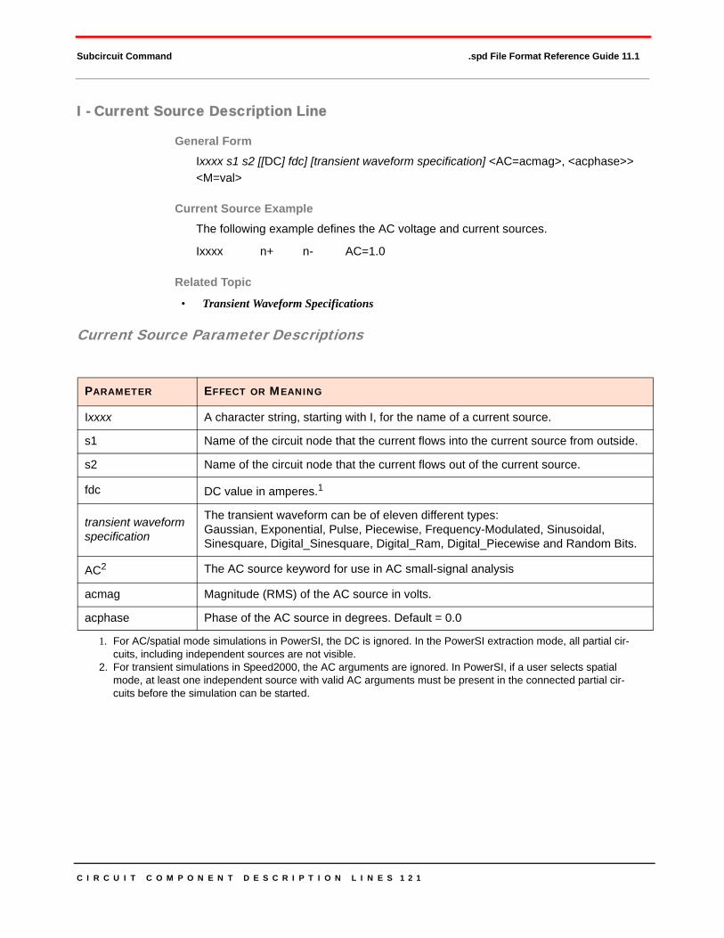
C I R C U I T C O M P O N E N T D E S C R I P T I O N L I N E S 1 2 1
Subcircuit Command .spd File Format Reference Guide 11.1
I - Current Source Description Line
General FormIxxxx s1 s2 [[DC] fdc] [transient waveform specification] <AC=acmag>, <acphase>><M=val>
Current Source ExampleThe following example defines the AC voltage and current sources.
Ixxxx n+ n- AC=1.0
Related Topic
• Transient Waveform Specifications
Current Source Parameter Descriptions
PARAMETER EFFECT OR MEANING
Ixxxx A character string, starting with I, for the name of a current source.
s1 Name of the circuit node that the current flows into the current source from outside.
s2 Name of the circuit node that the current flows out of the current source.
fdc DC value in amperes.1
transient waveform specification
The transient waveform can be of eleven different types: Gaussian, Exponential, Pulse, Piecewise, Frequency-Modulated, Sinusoidal, Sinesquare, Digital_Sinesquare, Digital_Ram, Digital_Piecewise and Random Bits.
AC2 The AC source keyword for use in AC small-signal analysis
acmag Magnitude (RMS) of the AC source in volts.
acphase Phase of the AC source in degrees. Default = 0.0
1. For AC/spatial mode simulations in PowerSI, the DC is ignored. In the PowerSI extraction mode, all partial cir-cuits, including independent sources are not visible.
2. For transient simulations in Speed2000, the AC arguments are ignored. In PowerSI, if a user selects spatial mode, at least one independent source with valid AC arguments must be present in the connected partial cir-cuits before the simulation can be started.

C I R C U I T C O M P O N E N T D E S C R I P T I O N L I N E S 1 2 2
Subcircuit Command .spd File Format Reference Guide 11.1
K - Mutual Inductor Description Line
General Form for Mathematical ExpressionKxxxx Inductor1 Inductor2 Value
In the following example, phase dot is on node 1 of Inductor L11 and on Node 21 of Inductor L18.
Mutual Inductor ExampleL11 1 2 1n
L18 21 24 2n
Ka L11 L12 0.6
Mutual Inductor Parameter Descriptions
NOTE!The phase dot convention is used to determine the sign of the mutual inductance.
Within the .spd file the phase dot is on the first node of the inductor de-scription line.
PARAMETER EFFECT OR MEANING
Kxxxx A character string, starting with K, for the name of a mutual inductor.
Inductor1 Name of one coupled inductor.
Inductor2 Name of the other coupled inductor.
Value
Coupling coefficient of Inductor1 and Inductor2.The mutual inductance value is cal-culated as: Coupling_Coefficient × sqrt ( L1 × L2) where L1 = inductance of inductor 1 and L2 = inductance of the other inductor.

C I R C U I T C O M P O N E N T D E S C R I P T I O N L I N E S 1 2 3
Subcircuit Command .spd File Format Reference Guide 11.1
_Lmatrix - Inductor Matrix Description Line
General Form_Lmatrixxxxx N = n1 file = s1 Node1 Node2 … NodeM
Each line of the file describes one self or mutual inductor with the following format:
branchi branchj Value
_LMatrix Indicator Example 1The following is an example of the _Lmatrix statement as it appears in a .spd file andthe cmat.dat file that it calls.
L-Matrix Indicator Example 2Circuit description lines 3-5 are equivalent to line 12. Lines 20-22 represent the data file.The use of a data file permits more than one .spd file to use the same matrix.
1: V 1 0 pulse ( 0 1 0 10n 10n 10n 1)
2: R1 1 2 1
3: L1 2 0 1n
4: L2 3 0 1n
5: K L1 L2 0.1
6: R2 3 0 1
10: V 1 0 pulse ( 0 1 0 10n 10n 10n 1)
11: R1 1 2 112: _Lmatrix N=2 file = lmat.dat 2 0 3 013: R2 3 0 1where the content of lmat.dat file is: 20: 1 1 1n21: 2 2 1n22: 1 2 0.1
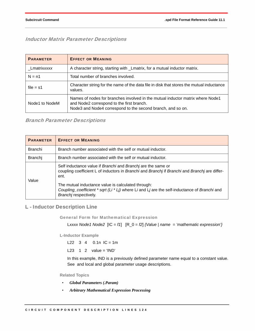
C I R C U I T C O M P O N E N T D E S C R I P T I O N L I N E S 1 2 4
Subcircuit Command .spd File Format Reference Guide 11.1
Inductor Matrix Parameter Descriptions
Branch Parameter Descriptions
L - Inductor Description Line
General Form for Mathematical ExpressionLxxxx Node1 Node2 [IC = f1] [R_0 = f2] {Value | name = ‘mathematic expression’}
L-Inductor ExampleL22 3 4 0.1n IC = 1m
L23 1 2 value = ‘IND’
In this example, IND is a previously defined parameter name equal to a constant value.See and local and global parameter usage descriptions.
Related Topics
• Global Parameters (.Param)
• Arbitrary Mathematical Expression Processing
PARAMETER EFFECT OR MEANING
_Lmatrixxxxx A character string, starting with _Lmatrix, for a mutual inductor matrix.
N = n1 Total number of branches involved.
file = s1 Character string for the name of the data file in disk that stores the mutual inductance values.
Node1 to NodeMNames of nodes for branches involved in the mutual inductor matrix where Node1 and Node2 correspond to the first branch. Node3 and Node4 correspond to the second branch, and so on.
PARAMETER EFFECT OR MEANING
Branchi Branch number associated with the self or mutual inductor.
Branchj Branch number associated with the self or mutual inductor.
Value
Self inductance value if Branchi and Branchj are the same orcoupling coefficient L of inductors in Branchi and Branchj if Branchi and Branchj are differ-ent.
The mutual inductance value is calculated through: Coupling_coefficient * sqrt (Li * Lj) where Li and Lj are the self-inductance of Branchi and Branchj respectively.
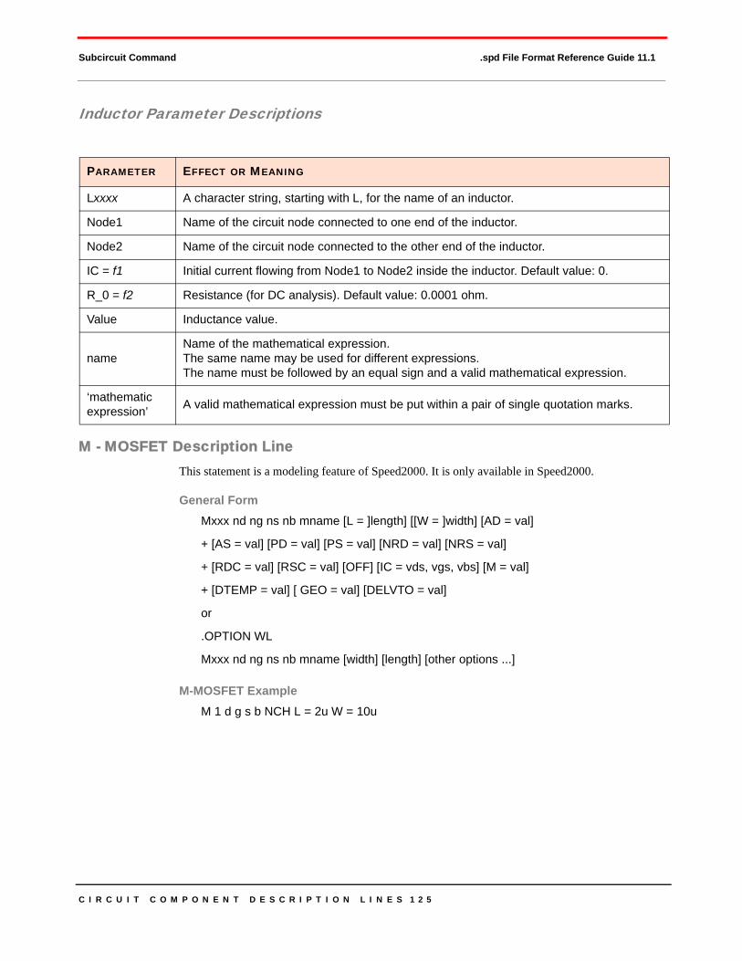
C I R C U I T C O M P O N E N T D E S C R I P T I O N L I N E S 1 2 5
Subcircuit Command .spd File Format Reference Guide 11.1
Inductor Parameter Descriptions
M - MOSFET Description LineThis statement is a modeling feature of Speed2000. It is only available in Speed2000.
General FormMxxx nd ng ns nb mname [L = ]length] [[W = ]width] [AD = val]
+ [AS = val] [PD = val] [PS = val] [NRD = val] [NRS = val]
+ [RDC = val] [RSC = val] [OFF] [IC = vds, vgs, vbs] [M = val]
+ [DTEMP = val] [ GEO = val] [DELVTO = val]
or
.OPTION WL
Mxxx nd ng ns nb mname [width] [length] [other options ...]
M-MOSFET ExampleM 1 d g s b NCH L = 2u W = 10u
PARAMETER EFFECT OR MEANING
Lxxxx A character string, starting with L, for the name of an inductor.
Node1 Name of the circuit node connected to one end of the inductor.
Node2 Name of the circuit node connected to the other end of the inductor.
IC = f1 Initial current flowing from Node1 to Node2 inside the inductor. Default value: 0.
R_0 = f2 Resistance (for DC analysis). Default value: 0.0001 ohm.
Value Inductance value.
name Name of the mathematical expression. The same name may be used for different expressions. The name must be followed by an equal sign and a valid mathematical expression.
‘mathematic expression’ A valid mathematical expression must be put within a pair of single quotation marks.

C I R C U I T C O M P O N E N T D E S C R I P T I O N L I N E S 1 2 6
Subcircuit Command .spd File Format Reference Guide 11.1
MOSFET Parameter Descriptions
NAME DEFAULT DESCRIPTION
Mxxx - MOSFET element name. Must begin with “M”.
nd - Drain node.
ng - Gate node.
ns - Source node.
nb - Bulk node, which is NOT optional.
mname - Referenced MOSFET model name.
L DEFL MOSFET channel length in meters. Maximum: 0.1m.
W DEFW MOSFET channel width in meters.
AD DEFAD if ACM=0 Drain diffusion area.
AS DEFAS if ACM=0 Source diffusion area. Overrides DEFAS in OPTIONS statement.
PD DEFPD if ACM=0 or 10.0 if ACM=2 or 3 Perimeter of the drain junction, including the channel edge.
PS DEFPS if ACM=0 or 10.0 if ACM=2 or 3 Perimeter of the source junction, including the channel edge.
NRD DEFNRD if ACM=0 or 10.0 if ACM=2 or 3 Number of squares of drain diffusion for resistance calculations.
NRS DEFNRS if ACM=0 or 10.0 if ACM=2 or 3 Number of squares of source diffusion for resistance cogitations.
RDC 0.0 Additional drain resistance due to contact resistance with units of ohms. Overrides RDC in the MOSFET model card.
RSC 0.0 Additional source resistance due to contact resistance with units of ohms. Overrides RSC in the MOSFET model card.
OFF ON. If written, sets initial condition to OFF in DC analysis.
IC=vds, vgs, vbs - Initial voltage across the external drain and source (vds), gate and
source (vgs), and bulk and source terminals (vbs).
M 1.0 Multiplier to simulate multiple MOSFETs in parallel.
DTEMP 0.0 The difference between the element temperature and the circuit temperature in Celsius.
GEO 0.0 Source / drain sharing selector for MOSFET model parameter value ACM=3.
DELVTO 0.0 Zero-based threshold voltage shift.

C I R C U I T C O M P O N E N T D E S C R I P T I O N L I N E S 1 2 7
Subcircuit Command .spd File Format Reference Guide 11.1
R - Resistor Description Line
General FormRxxxx Node1 Node2 [mname] R [ TC1 [ TC2 [ SCALE ]]] [ M=val]
+ [DTEMP = val] [L=val] [W=val]
Rxxx Node1 Node 2 [mname] [R = ] val|’equation’ [[TC1 = ]val]
+ [[TC2 = ] val ] [[ SCALE ] = val ] [ M = val ]
+ [ DTEMP = val ] [ L = val ] [ W = val ]
R-Resistor Example 1 R 4 2 844m
R-Resistor Example 2In this example, resistor, R1, has a value in the form of a mathematical expression.
Both V0 and I0 must be constant parameters.
R1 1 2 R = ' V0 / I0 '
NOTE!Voltage variables and Current variables may not appear in math ex-pressions for R, L and C components.
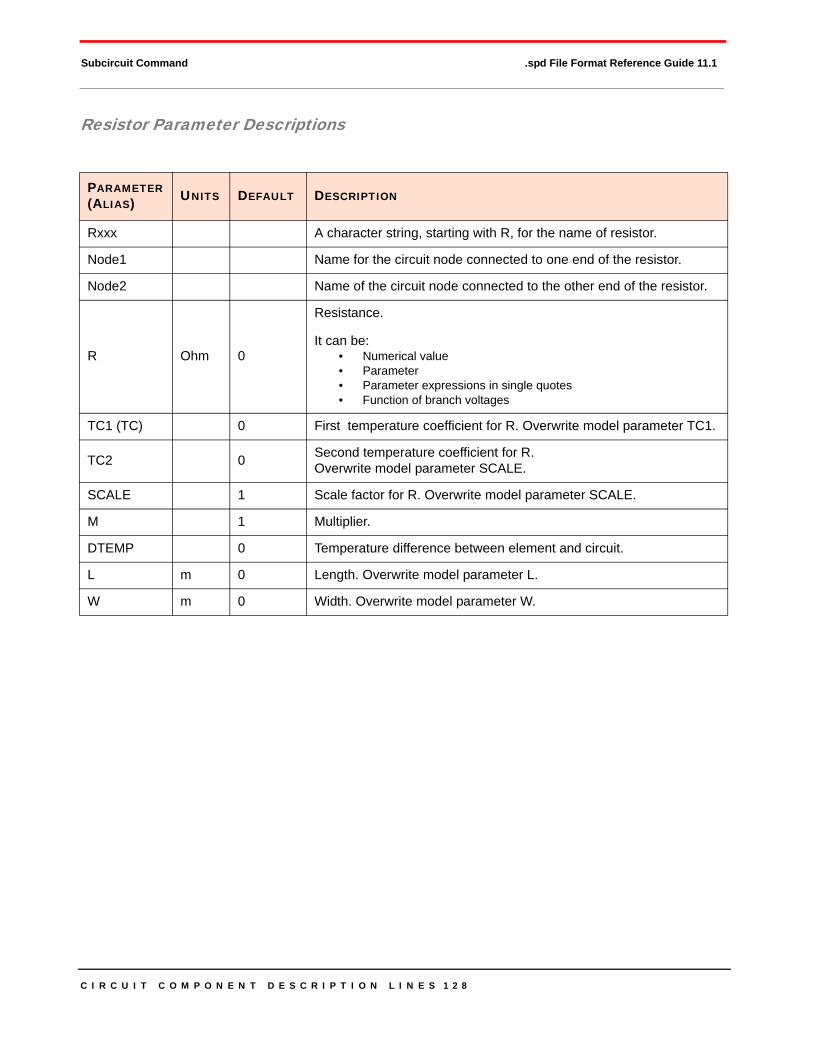
C I R C U I T C O M P O N E N T D E S C R I P T I O N L I N E S 1 2 8
Subcircuit Command .spd File Format Reference Guide 11.1
Resistor Parameter Descriptions
PARAMETER (ALIAS) UNITS DEFAULT DESCRIPTION
Rxxx A character string, starting with R, for the name of resistor.
Node1 Name for the circuit node connected to one end of the resistor.
Node2 Name of the circuit node connected to the other end of the resistor.
R Ohm 0
Resistance.
It can be:• Numerical value• Parameter• Parameter expressions in single quotes• Function of branch voltages
TC1 (TC) 0 First temperature coefficient for R. Overwrite model parameter TC1.
TC2 0 Second temperature coefficient for R. Overwrite model parameter SCALE.
SCALE 1 Scale factor for R. Overwrite model parameter SCALE.
M 1 Multiplier.
DTEMP 0 Temperature difference between element and circuit.
L m 0 Length. Overwrite model parameter L.
W m 0 Width. Overwrite model parameter W.

C I R C U I T C O M P O N E N T D E S C R I P T I O N L I N E S 1 2 9
Subcircuit Command .spd File Format Reference Guide 11.1
S - S Parameters Description Line
General Form for S ParametersSxxx {nd1 n2 ... ndN ndRef | nd1 ndRef1 nd2 ndRef2... ndN ndRef}
+ {MNAME=Smodel_name | model=data_file}
+ [fmax=f_max] [fbase=f_base]
S Parameter Descriptions
PARAMETER EFFECT OR MEANING
nd1 nd2 ... ndN ndRef Node names. nd1 nd2 ... ndN: Port nodes. ndRef: Reference node.
nd1 ndRef1 nd2 ndRef2...ndN ndRef
Node names. nd1 nd2 ... ndN: Port nodes. ndRef1 ndRef2... ndRef: Reference nodes.
MNAME Name of S model, which is defined in .model description lines.
ModelData file name. Speed2000 supports BNP, TOUTCHSTONE and RFM files, while PowerSI only supports BNP and TOUTCHSTONE files.
FmaxThe max frequency of inverse Fourier Transform when using BNP or TOUCHSTONE files. Default Fmax = 1/ (simulation time interval).
FbaseThe base frequency of inverse Fourier Transform when using BNP or TOUCHSTONE files.
Default Fbase = 1/ (simulation period).

C I R C U I T C O M P O N E N T D E S C R I P T I O N L I N E S 1 3 0
Subcircuit Command .spd File Format Reference Guide 11.1
T - Transmission Line Description LineThere are two forms for the Transmission Line Description line: PowerSI and SPDSIM.
General Form for PowerSITxxx Node1 Node2 Node3 Node4 Z0=f1 TD=f2 [R_0 = f3]
General Form for SPDSIMTxxx Node1 Node2 Node3 Node4 Z0=f1 TD=f2 [R_0 = f3] [L = f4]
Transmission ExampleA transmission line with 50 Ohms characteristic impedance, and a 3-ns propagationdelay connected between circuit nodes: In, Gnd and Out, Gnd.
T1234 In Gnd Out Gnd Z0=50 TD=3n
Transmission Parameter Descriptions
PARAMETER EFFECT OR MEANING
Txxxx A character string, starting with T, for the name of a transmission line.
Node1, Node2Names of the circuit node connected to one end of the transmission line. Voltage measured at this end is by the potential at Node1 minus the potential at Node2.
Node3, Node41Names of the circuit node connected to the other end of the transmission line. Voltage measured at this end is by the potential at Node3 minus the potential at Node4.
Z0=f1 Characteristic impedance in Ohms. Note: character is zero.
TD=f2 Transmission delay per unit length in seconds / meter.
R_0=f3DC Resistance for DC analysis. Character is zero.Default: 0.0001 Ohm.
L=f4 Physical length of transmission line in meters. Default L = 1.
1. For PowerSI: If the node names for Node2 and Node4 are different, a warning is given to the user: “Assigning the input reference node and the output reference node of a transmission line to a different circuit node, may lead to incorrect simulation results.”

C I R C U I T C O M P O N E N T D E S C R I P T I O N L I N E S 1 3 1
Subcircuit Command .spd File Format Reference Guide 11.1
V - Voltage Source Description Line
General FormVxxxx s1 s2 [ [DC] fdc] [transient waveform specification] [R_0=fr ]<AC=acmag><acphase><M=val>
Voltage Source ExampleThe following example defines the AC voltage source.
Vxxxx n+ n- AC=1.0,90
Related Topic
• Transient Waveform Specifications
Voltage Source Parameter Descriptions
PARAMETER EFFECT OR MEANING
Vxxxx A character string, starting with V, for the name of a voltage source.
s1 Name of the circuit node connected to the positive end of the voltage source.
s2 Name of the circuit node connected to the negative end of the voltage source.
fdc DC value in volts.
transient waveformspecification
The transient waveform can be of eleven different types: Gaussian, Exponential, Pulse, Piecewise, Frequency-Modulated, Sinusoidal, Sinesquare, Digital_Sinesquare, Digital_Ramp, Digital_Piecewise and Random Bits.
R_0= fr1 Inner resistance in ohms.
AC2 The AC source keyword for use in AC small-signal analysis
acmag Magnitude (RMS) of the AC source in amperes.
acphase Phase of the AC source in degrees. Default = 0.0
M The multiplier used for simulating multiple parallel current sources. The source current value is multiplied by M. Default = 1.0
1. This value is ignored by PowerSI2. For transient simulations in Speed2000, the AC arguments are ignored. In PowerSI, if a user selects spatial
mode, at least one independent source with valid AC arguments must be present in the connected partial cir-cuits before the simulation can be started.
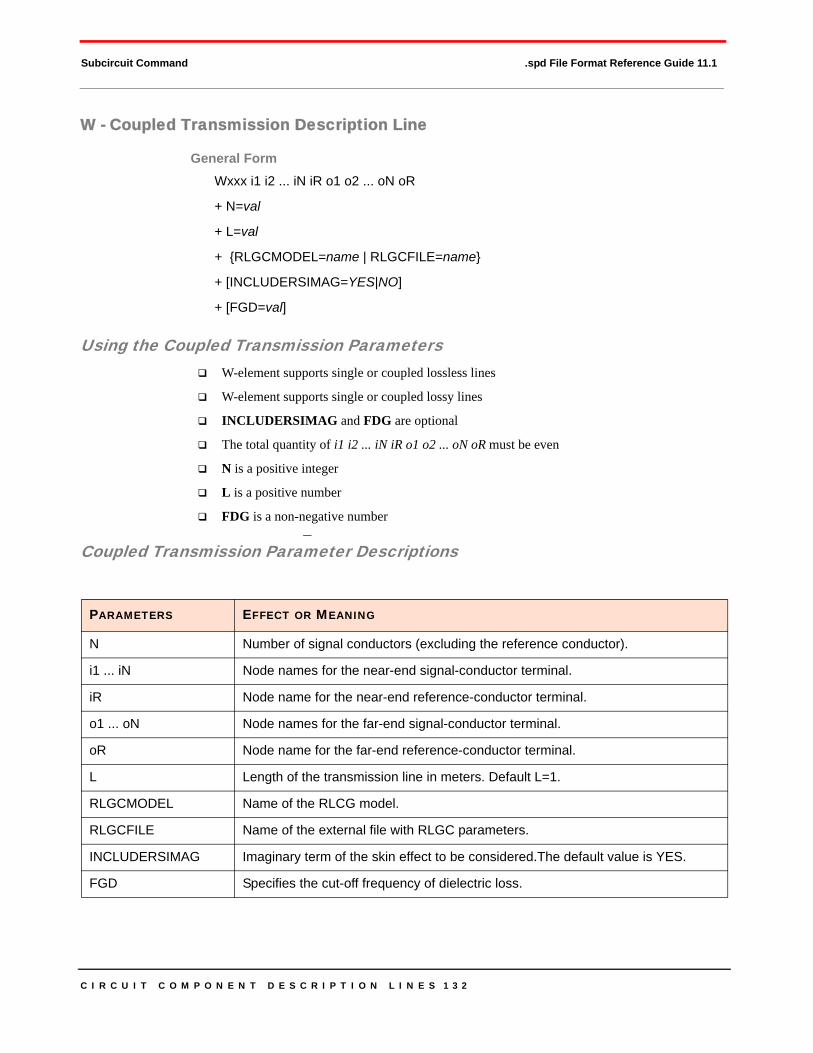
C I R C U I T C O M P O N E N T D E S C R I P T I O N L I N E S 1 3 2
Subcircuit Command .spd File Format Reference Guide 11.1
W - Coupled Transmission Description Line
General FormWxxx i1 i2 ... iN iR o1 o2 ... oN oR
+ N=val
+ L=val
+ {RLGCMODEL=name | RLGCFILE=name}
+ [INCLUDERSIMAG=YES|NO]
+ [FGD=val]
Using the Coupled Transmission ParametersW-element supports single or coupled lossless lines
W-element supports single or coupled lossy lines
INCLUDERSIMAG and FDG are optional
The total quantity of i1 i2 ... iN iR o1 o2 ... oN oR must be even
N is a positive integer
L is a positive number
FDG is a non-negative number
Coupled Transmission Parameter Descriptions
PARAMETERS EFFECT OR MEANING
N Number of signal conductors (excluding the reference conductor).
i1 ... iN Node names for the near-end signal-conductor terminal.
iR Node name for the near-end reference-conductor terminal.
o1 ... oN Node names for the far-end signal-conductor terminal.
oR Node name for the far-end reference-conductor terminal.
L Length of the transmission line in meters. Default L=1.
RLGCMODEL Name of the RLCG model.
RLGCFILE Name of the external file with RLGC parameters.
INCLUDERSIMAG Imaginary term of the skin effect to be considered.The default value is YES.
FGD Specifies the cut-off frequency of dielectric loss.
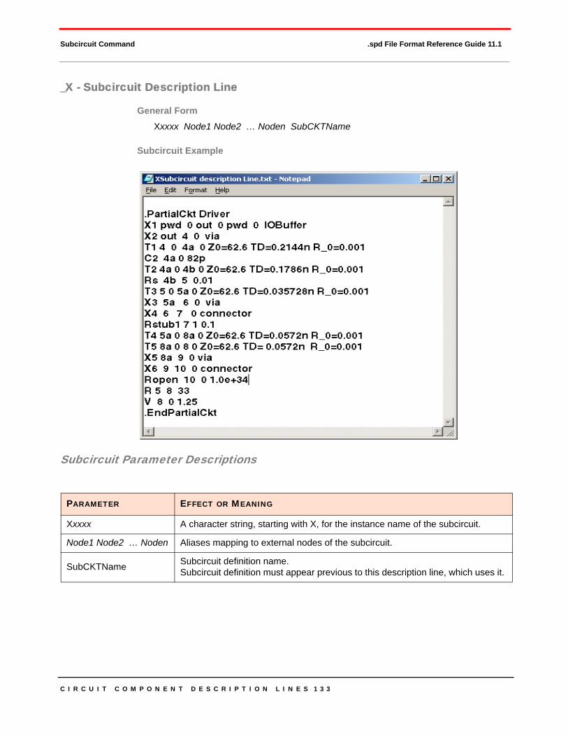
C I R C U I T C O M P O N E N T D E S C R I P T I O N L I N E S 1 3 3
Subcircuit Command .spd File Format Reference Guide 11.1
_X - Subcircuit Description Line
General FormXxxxx Node1 Node2 … Noden SubCKTName
Subcircuit Example
Subcircuit Parameter Descriptions
PARAMETER EFFECT OR MEANING
Xxxxx A character string, starting with X, for the instance name of the subcircuit.
Node1 Node2 … Noden Aliases mapping to external nodes of the subcircuit.
SubCKTName Subcircuit definition name. Subcircuit definition must appear previous to this description line, which uses it.

C I R C U I T C O M P O N E N T D E S C R I P T I O N L I N E S 1 3 4
Subcircuit Command .spd File Format Reference Guide 11.1
Device Model Options (.Option)In the device model simulation options can modify various aspects, including parameter defaults and integration methods.
General Form.Option {OptionName} {OptionName = value }
Device Model Option Parameter Descriptions
NOTE! The .Option {OptionName} can only be used for WL.
OPTION NAME DEFAULT DESCRIPTION
WLSyntax:.option WL or.option WL=value
0WL not specified
Reverses the order of width and length in MOSFET element state-ment if L= and W= are not written. Default assigns the first value to length and the second value to width.
SCALE 1 Scale element parameters.
SCALM 1 Scale model parameters.
DEFL 1e-4 Default MOSFET channel length.
DWFW 1e-4 Default MOSFET channel width.
DEFAD 0 Default MOSFET drain diode area.
DEFAS 0 Default MOSFET source diode area.
DEFPD 0 Default MOSFET drain diode perimeter.
DEFPS 0 Default MOSFET source code perimeter.
DEFNRD 0 Default number of squares of the drain resistor.
DEFNRS 0 Default number of squares of the source resistor.
EPSMIN 1e-28 Smallest number a computer can add or subtract.
TNOM 25 Reference temperature of model cards.
METHOD TRAP MOSFET numerical integration method in transient analysis. Can be GEAR or TRAP.

C I R C U I T C O M P O N E N T D E S C R I P T I O N L I N E S 1 3 5
Subcircuit Command .spd File Format Reference Guide 11.1
Device Temperatures (.Temp)The.TEMP statement sets the temperature for all the semiconductor devices.
The individual element temperature is calculated by:
Temperature set in the .temp statement + DTEMP element parameter
General Form.TEMP temperature
Mutual Capacitor MatricesEach line of the data file describes a self or mutual capacitor. The default mutual capacitance value is zero. Only the non-zero mutual capacitance values need to be listed.
General FormNode1 Node2 Value
Example 1 for Mutual Capacitor MatricesThe _Cmatrix statement as it appears in a .spd file and the cmat.dat file that it calls.
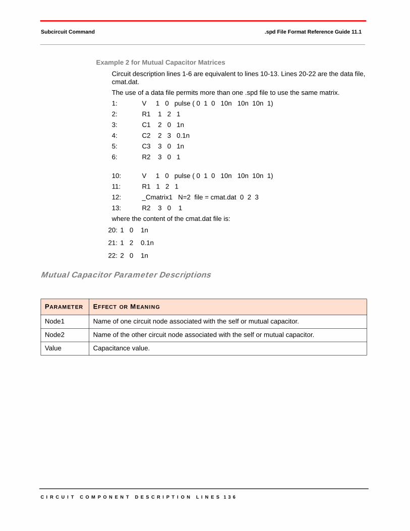
C I R C U I T C O M P O N E N T D E S C R I P T I O N L I N E S 1 3 6
Subcircuit Command .spd File Format Reference Guide 11.1
Example 2 for Mutual Capacitor MatricesCircuit description lines 1-6 are equivalent to lines 10-13. Lines 20-22 are the data file, cmat.dat. The use of a data file permits more than one .spd file to use the same matrix. 1: V 1 0 pulse ( 0 1 0 10n 10n 10n 1)2: R1 1 2 13: C1 2 0 1n4: C2 2 3 0.1n5: C3 3 0 1n6: R2 3 0 1
10: V 1 0 pulse ( 0 1 0 10n 10n 10n 1)11: R1 1 2 112: _Cmatrix1 N=2 file = cmat.dat 0 2 3 13: R2 3 0 1where the content of the cmat.dat file is:
20: 1 0 1n
21: 1 2 0.1n
22: 2 0 1n
Mutual Capacitor Parameter Descriptions
PARAMETER EFFECT OR MEANING
Node1 Name of one circuit node associated with the self or mutual capacitor.
Node2 Name of the other circuit node associated with the self or mutual capacitor.
Value Capacitance value.

C I R C U I T C O M P O N E N T D E S C R I P T I O N L I N E S 1 3 7
Transient Waveform Specifications .spd File Format Reference Guide 11.1
TRANSIENT WAVEFORM SPECIFICATIONSThere are ten transient waveform specifications.
Digital_PWL WaveformDigital_Ramp WaveformDigital_Sinesquare WaveformExponential WaveformFrequency-Modulated WaveformGaussian WaveformPiecewise Linear WaveformPulse WaveformSinesquare WaveformSinusoidal WaveformRandom Bits Waveform
Digital_PWL Waveform
General FormDigital_PWL(FT1, FI1, FT2, FI2,...FTN, FIN)+ Pattern=( {0|1}, {0|1},...{0|1} ) [T0 = t0] or Digital_PWL FILE=s1 + Pattern=( {0|1}, {0|1},...{0|1} ) [T0 = t0]
Pattern Bit ChangeThe simulation tool checks the pattern bit change at:
t0+M*bit_time (M=1,2,3,...)
If 0->0, then use the value fi1l for (t0 + M * bit_time) < t < (t0 + ( M + 1 ) * bit_time).
If 0->1, then use the first half of the PWL data for (t0 + M * bit_time) < t < (t0 + ( M + 1 ) * bit_time).
If 1->0, then use the second half of the PWL data for (t0 + M * bit_time) < t < (t0 + ( M + 1 ) * bit_time).
If 1->1, then use the value ftm (ftm=bit_time) for (t0 + M * bit_time) < t < (t0 + ( M + 1 ) * bit_time).
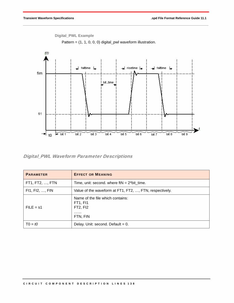
C I R C U I T C O M P O N E N T D E S C R I P T I O N L I N E S 1 3 8
Transient Waveform Specifications .spd File Format Reference Guide 11.1
Digital_PWL ExamplePattern = (1, 1, 0, 0, 0) digital_pwl waveform illustration.
Digital_PWL Waveform Parameter Descriptions
PARAMETER EFFECT OR MEANING
FT1, FT2, …, FTN Time, unit: second. where ftN = 2*bit_time.
FI1, FI2, …, FIN Value of the waveform at FT1, FT2, …, FTN, respectively.
FILE = s1
Name of the file which contains:FT1, FI1FT2, FI2……FTN, FIN
T0 = t0 Delay. Unit: second. Default = 0.

C I R C U I T C O M P O N E N T D E S C R I P T I O N L I N E S 1 3 9
Transient Waveform Specifications .spd File Format Reference Guide 11.1
Digital_Ramp Waveform
General FormDigital_Ramp (f1, f2, f3, f4, f5, f6)
+ Pattern = ( {0|1}, {0|1}, {0|1}, …, {0|1} )
Digital Ramp Waveform ExamplePattern = (1, 1, 0, 0, 0) digital_ramp waveform illustration
delay bit 1 bit 2 bit 3 bit 4 bit 5 bit 6 bit 7 bit 8 bit 9
falltime risetimehighvalue
f(t)
t
lowvalue
falltime
bitwidth
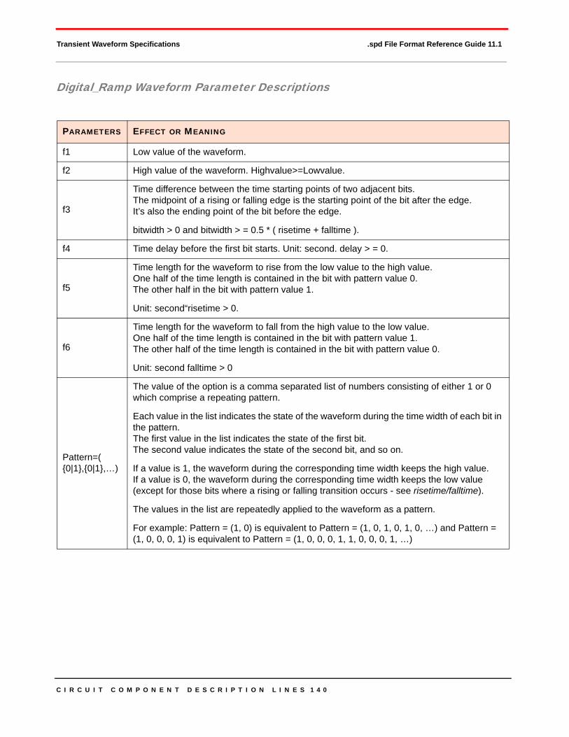
C I R C U I T C O M P O N E N T D E S C R I P T I O N L I N E S 1 4 0
Transient Waveform Specifications .spd File Format Reference Guide 11.1
Digital_Ramp Waveform Parameter Descriptions
PARAMETERS EFFECT OR MEANING
f1 Low value of the waveform.
f2 High value of the waveform. Highvalue>=Lowvalue.
f3
Time difference between the time starting points of two adjacent bits. The midpoint of a rising or falling edge is the starting point of the bit after the edge. It’s also the ending point of the bit before the edge.
bitwidth > 0 and bitwidth > = 0.5 * ( risetime + falltime ).
f4 Time delay before the first bit starts. Unit: second. delay > = 0.
f5
Time length for the waveform to rise from the low value to the high value. One half of the time length is contained in the bit with pattern value 0. The other half in the bit with pattern value 1.
Unit: second“risetime > 0.
f6
Time length for the waveform to fall from the high value to the low value. One half of the time length is contained in the bit with pattern value 1. The other half of the time length is contained in the bit with pattern value 0.
Unit: second falltime > 0
Pattern=( {0|1},{0|1},…)
The value of the option is a comma separated list of numbers consisting of either 1 or 0 which comprise a repeating pattern.
Each value in the list indicates the state of the waveform during the time width of each bit in the pattern.The first value in the list indicates the state of the first bit. The second value indicates the state of the second bit, and so on.
If a value is 1, the waveform during the corresponding time width keeps the high value. If a value is 0, the waveform during the corresponding time width keeps the low value (except for those bits where a rising or falling transition occurs - see risetime/falltime).
The values in the list are repeatedly applied to the waveform as a pattern.
For example: Pattern = (1, 0) is equivalent to Pattern = (1, 0, 1, 0, 1, 0, …) and Pattern = (1, 0, 0, 0, 1) is equivalent to Pattern = (1, 0, 0, 0, 1, 1, 0, 0, 0, 1, …)

C I R C U I T C O M P O N E N T D E S C R I P T I O N L I N E S 1 4 1
Transient Waveform Specifications .spd File Format Reference Guide 11.1
Digital_Sinesquare Waveform
General FormDigital_Sinesquare (f1, f2, f3, f4, f5, f6)
+ Pattern = ( {0|1}, {0|1}, {0|1}, …, {0|1} )
Digital Sinesquare Waveform ExamplePattern = (1, 1, 0, 0, 0) digital_sinesquare waveform illustration
delay bit 1 bit 2 bit 3 bit 4 bit 5 bit 6 bit 7 bit 8 bit 9
falltime risetimehighvalue
f(t)
t
lowvalue
falltime
bitwidth

C I R C U I T C O M P O N E N T D E S C R I P T I O N L I N E S 1 4 2
Transient Waveform Specifications .spd File Format Reference Guide 11.1
Digital_Sinesquare Waveform Parameter Descriptions
PARAMETERS EFFECT OR MEANING
f1 Low value of the waveform.
f2 High value of the waveform. Highvalue>=Lowvalue.
f3
Time difference between the time starting points of two adjacent bits. Midpoint of a rising or falling edge is the starting point of the bit after the edge. Also the ending point of the bit before the edge.
Unit: second. bitwidth > 0 and bitwidth > = 0.5 * ( risetime + falltime ).
f4 Time delay before the first bit starts. Unit: second; Delay > = 0.
f5
Time length for the waveform to rise from the low value to the high value. One half of the time length is contained in the bit with pattern value 0. The other half of the time length is contained in the bit with pattern value 1.
Unit: second risetime > 0.
f6
Time length for the waveform to fall from the high value to the low value. One half of the time length is contained in the bit with pattern value 1. The other half in the bit with pattern value 0.
Unit: second falltime > 0.
Pattern=( {0|1},{0|1},…)
The value of the option is a comma separated list of numbers consisting of either 1 or 0 which comprise a repeating pattern.
Each value in the list indicates the state of the waveform during the time width of each bit in the pattern. The first value in the list indicates the state of the first bit. The second value indicates the state of the second bit, and so on.
If a value is 1, the waveform during the corresponding time width keeps the high value. If a value is 0, the waveform during the corresponding time width keeps the low value (except for those bits where a rising or falling transition occurs - see risetime/falltime).
The values in the list are repeatedly applied to the waveform as a pattern.
For example: Pattern = (1, 0) is equivalent to Pattern = (1, 0, 1, 0, 1, 0, …) and Pattern = (1, 0, 0, 0, 1) is equivalent to Pattern = (1, 0, 0, 0, 1, 1, 0, 0, 0, 1, …).

C I R C U I T C O M P O N E N T D E S C R I P T I O N L I N E S 1 4 3
Transient Waveform Specifications .spd File Format Reference Guide 11.1
Exponential Waveform
General FormEXP( f1 f2 [f3] [f4] [f5] [f6] )
Waveform Amplitude
Exponential Waveform Example
Exponential Waveform Parameter Descriptions
f1 (t<f3)
f1+(f2-f1)(1-exp(-(t-f3)/f4)) (f3<t<f5)
f1+(f2-f1)(1-exp(-(t-f3)/f4)-(1-exp(-(t-f5)/f6))) (t>f5)
f1
f2
f3
f4
f5 t
f6
63.2% 63.2%
PARAMETERS EFFECT OR MEANING
f1 Initial value.
f2 Peak value.
f3 Rise(fall) delay, unit: sec., default: 0.
f4 Rise(fall) time constant, unit: sec., default: simulation time step.
f5 Fall(rise) delay, unit: sec., default: f3 + simulation time step.
f6 Fall(rise) time constant, unit: sec., default: simulation time step.

C I R C U I T C O M P O N E N T D E S C R I P T I O N L I N E S 1 4 4
Transient Waveform Specifications .spd File Format Reference Guide 11.1
Frequency-Modulated Waveform
General FormSFFM ( f1 f2 [f3] [f4] [f5] )
Waveform Amplitudef1+f2 sin(2π f3 t +f4 sin(2π f5 t))
Frequency Modulated Waveform Example
Frequency Modulated Waveform Parameter Descriptions
f2
f1
t
PARAMETERS EFFECT OR MEANING
f1 Offset value
f2 Peak amplitude of value.
f3 Carrier frequency, unit: hertz. Default: 0.
f4 Modulation index. Default: 0.
f5 Modulation frequency, unit: hertz. Default: 0.
C I R C U I T C O M P O N E N T D E S C R I P T I O N L I N E S 1 4 5
Transient Waveform Specifications .spd File Format Reference Guide 11.1
Gaussian Waveform
General FormGAUSSIAN ( F1 F2 F3 F4 [F5] )
Waveform Amplitude Examplef1+(f2-f1) exp( - ( ( t - f3) /(0.2887* f4 ))2 ) (in the first period)
Gaussian Waveform Parameter Descriptions
f1
f2
f3
f4
f5
t
PARAMETERS EFFECT OR MEANING
f1 Initial value
f2 Peak value
f3 Time delay, unit: sec., suggested value: 1.3~1.5 times f4
f4 Pulse width, unit: sec., measured at 5% of (peak value - initial value)
f5 Period, unit: sec. Default: infinity.

C I R C U I T C O M P O N E N T D E S C R I P T I O N L I N E S 1 4 6
Transient Waveform Specifications .spd File Format Reference Guide 11.1
Piecewise Linear Waveform
General FormPWL ( ft1 fi1 ft2 fi2 ft3 fi3 ft4 fi4 … [R[=repeat]])
or
PWL FILE=s1 [R[=repeat]])
Piecewise Linear Waveform Example
Piecewise Linear Waveform Parameter Descriptions
NOTE!
If there are N pairs of time and values: with no keyword, R: Waveform amplitude = fi1 (t < ft1) fiN (t > ftN)
For keyword R, with no argument, the source repeats from the begin-ning of the function. Repeat is the time, in units of seconds, which specifies the start point of the waveform to repeat.
This time needs to be less than the greatest time point, ftn.
tft1 ft2 ft4ft3 ftn
fi1
fi2 fi3
fi4
fin
PARAMETERS EFFECT OR MEANING
ft1, ft2, ft3, … Time, unit: second.
fi1, fi2, fi3, … Value of the waveform at ft1, ft2, ft3,… , respectively.
FILE=s1
Name of the file which contains: ft1 fi1 ft2 fi2 ft3 fi3
R=Repeat Time, unit: seconds which specify the start point of the repeating waveform.
C I R C U I T C O M P O N E N T D E S C R I P T I O N L I N E S 1 4 7
Transient Waveform Specifications .spd File Format Reference Guide 11.1
Pulse Waveform
General FormPULSE( f1 f2 [f3] [f4] [f5] [f6] [f7] )
Pulse Waveform Example
Pulse Waveform Parameter Descriptions
Waveform Amplitude Parameter Descriptions
f1
f2
f3 t
f4
f6
f5
f7
PARAMETERS EFFECT OR MEANING
f1 Initial value
f2 Peak value of the pulse.
f3 Delay, unit: sec., default: 0.
f4 Rise time, unit: sec., default: simulation time step.
f5 Fall time, unit: sec., default: simulation time step.
f6 Pulse width, unit: sec., default: infinity.
f7 Period, unit: sec., default: infinity.
PARAMETERS EFFECT OR MEANING
f1 (t<f3)
f1+(f2-f1)(t-f3)/f4 (f3<t<f3+f4)
f2 (f3+f4<t<f3+f4+f6)
f2-(f2-f1)(t-f3-f4-f6)/f5 (f3+f4+f6<t<f3+f4+f6+f5)
f1 (f3+f4+f6+f5<t<f3+f7)

C I R C U I T C O M P O N E N T D E S C R I P T I O N L I N E S 1 4 8
Transient Waveform Specifications .spd File Format Reference Guide 11.1
Sinesquare Waveform
General FormSINESQUARE( f1 f2 [f3] [f4] [f5] [f6] [f7] )
Sinesquare Waveform Example
Sinesquare Waveform Parameter Descriptions
f1
f2
t f3
f4
f6
f5
f7
PARAMETERS EFFECT OR MEANING
f1 Initial value
f2 Peak value
f3 Delay, unit: sec. Default: 0.
f4 Rise time, unit: sec. Default: simulation time step.
f5 Fall time, unit: sec. Default: simulation time step.
f6 Pulse width, unit: sec. Default: infinity. Time the waveform amplitude remains at f2.
f7 Period, unit: sec., default: infinity.

C I R C U I T C O M P O N E N T D E S C R I P T I O N L I N E S 1 4 9
Transient Waveform Specifications .spd File Format Reference Guide 11.1
Waveform Amplitude Parameter Descriptions
PARAMETERS EFFECT OR MEANING
f1 (t<f3)
f1+0.5(f2-f1)(1-cos(π(t-f3)/f4)) (f3<t<f3+f4)
f2 (f3+f4<t<f3+f4+f6)
f1+0.5(f2-f1)(1+cos(π(t-f3-f4-f6)/f5)) (f3+f4+f6<t<f3+f4+f6+f5)
f1 (f3+f4+f6+f5<t<f3+f7)
C I R C U I T C O M P O N E N T D E S C R I P T I O N L I N E S 1 5 0
Transient Waveform Specifications .spd File Format Reference Guide 11.1
Sinusoidal Waveform
General FormSIN( f1 f2 [f3] [f4] [f5] [f6] )
Sinusoidal Waveform Example
Sinesquare Waveform Equationf1+ f2 som ( 2π f6 / 360) ( t < f4)
Waveform amplitude = {f1+ f2 sin ( 2π ( f3 ( t - f4) + f6 / 360 ) ) exp (- ( t - f4 ) f5) ( t > f4 )
Sinusoidal Waveform Parameter Descriptions
Waveform Amplitude Parameter Descriptions
f1
f2
t f4
PARAMETERS EFFECT OR MEANING
f1 Offset value
f2 Peak amplitude of the sine function.
f3 Frequency, unit: hertz, default: 0.
f4 Delay, unit: sec., default: 0.
f5 Damping factor, unit: 1/sec., default: 0.
f6 Phase, unit: degree, default: 0.
PARAMETERS EFFECT OR MEANING
f1 + f2 sin (2π f6 / 360 ) ( t < f4)
f1 + f2 sin (2π ( f3 ( t - f4)+ f6 / 360 ) ) exp (- ( t-f4 ) f5 ) ( t > f4)
C I R C U I T C O M P O N E N T D E S C R I P T I O N L I N E S 1 5 1
Transient Waveform Specifications .spd File Format Reference Guide 11.1
Random Bits Waveform
General FormRandom_Bit (
+ f1
+ f2
+ {BITP=d_bitp | DATA_RATE=d_data_rate}
+ [DELAY = d_delay]
+ [TR=d_tr]
+ [TF = d_tf]
+ [POLY = i_poly]
+[SEED = i_seed]
+ [BITS = filename_bits]
+ [LEADBITS = filename_leadbits]
+ [JITTER=d_jit]
+ [NOISE=d_noise] )
+[CODE={8b10b | 64b66b}])
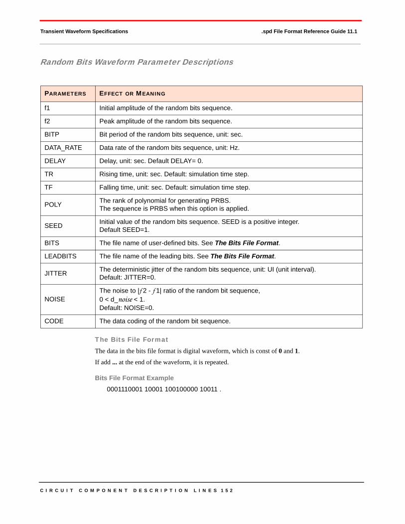
C I R C U I T C O M P O N E N T D E S C R I P T I O N L I N E S 1 5 2
Transient Waveform Specifications .spd File Format Reference Guide 11.1
Random Bits Waveform Parameter Descriptions
The Bits File FormatThe data in the bits file format is digital waveform, which is const of 0 and 1.
If add ... at the end of the waveform, it is repeated.
Bits File Format Example0001110001 10001 100100000 10011 .
PARAMETERS EFFECT OR MEANING
f1 Initial amplitude of the random bits sequence.
f2 Peak amplitude of the random bits sequence.
BITP Bit period of the random bits sequence, unit: sec.
DATA_RATE Data rate of the random bits sequence, unit: Hz.
DELAY Delay, unit: sec. Default DELAY= 0.
TR Rising time, unit: sec. Default: simulation time step.
TF Falling time, unit: sec. Default: simulation time step.
POLY The rank of polynomial for generating PRBS. The sequence is PRBS when this option is applied.
SEED Initial value of the random bits sequence. SEED is a positive integer. Default SEED=1.
BITS The file name of user-defined bits. See The Bits File Format.
LEADBITS The file name of the leading bits. See The Bits File Format.
JITTER The deterministic jitter of the random bits sequence, unit: UI (unit interval). Default: JITTER=0.
NOISEThe noise to |f 2 - f 1| ratio of the random bit sequence, 0 < d_noise < 1. Default: NOISE=0.
CODE The data coding of the random bit sequence.

C I R C U I T C O M P O N E N T D E S C R I P T I O N L I N E S 1 5 3
Transient Waveform Specifications .spd File Format Reference Guide 11.1
Examples of Source with Random Bits Waveform
Random Bits Waveform Example 1V1 1 2+ RANDOM_BIT (+ 0+ 0.5+ DATA_RATE = 5g+ POLY = 23+ TR = 0.01n+ TF = 0.01n+ JITTER=0.2+ NOISE=0.05)
Random Bits Waveform Example 2|1 1 2+ RANDOM_BIT (+ 0.5+ 1+ BITP= 0.2n+ DELAY = 0.1n+ TR = 0.01n+ TF = 0.01n+ JITTER = 0.1+ NOISE = 0.01)
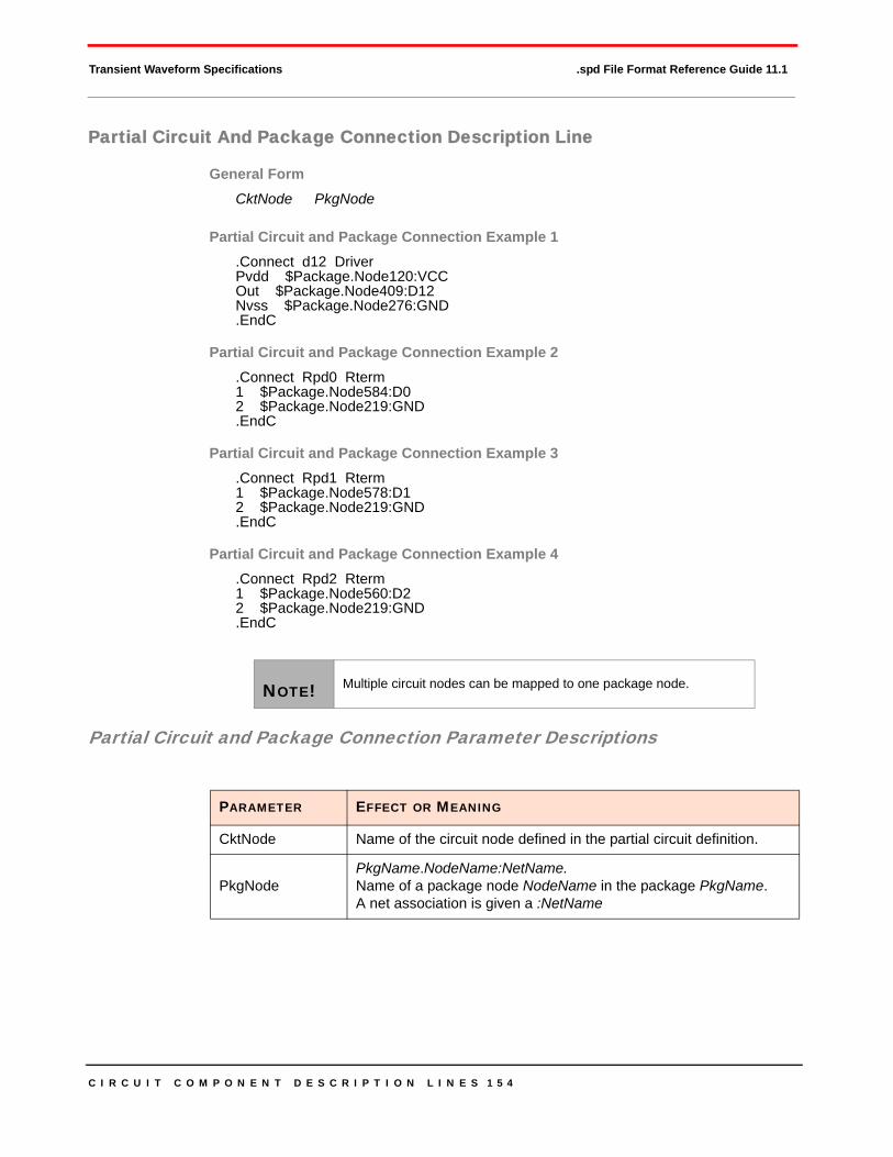
C I R C U I T C O M P O N E N T D E S C R I P T I O N L I N E S 1 5 4
Transient Waveform Specifications .spd File Format Reference Guide 11.1
Partial Circuit And Package Connection Description Line
General FormCktNode PkgNode
Partial Circuit and Package Connection Example 1.Connect d12 DriverPvdd $Package.Node120:VCCOut $Package.Node409:D12Nvss $Package.Node276:GND.EndC
Partial Circuit and Package Connection Example 2.Connect Rpd0 Rterm1 $Package.Node584:D02 $Package.Node219:GND.EndC
Partial Circuit and Package Connection Example 3.Connect Rpd1 Rterm1 $Package.Node578:D12 $Package.Node219:GND.EndC
Partial Circuit and Package Connection Example 4.Connect Rpd2 Rterm1 $Package.Node560:D22 $Package.Node219:GND.EndC
Partial Circuit and Package Connection Parameter Descriptions
NOTE! Multiple circuit nodes can be mapped to one package node.
PARAMETER EFFECT OR MEANING
CktNode Name of the circuit node defined in the partial circuit definition.
PkgNodePkgName.NodeName:NetName. Name of a package node NodeName in the package PkgName. A net association is given a :NetName

C I R C U I T C O M P O N E N T D E S C R I P T I O N L I N E S 1 5 5
Polynomial Functions in Nonlinear Circuit Elements .spd File Format Reference Guide 11.1
POLYNOMIAL FUNCTIONS IN NONLINEAR CIRCUIT ELEMENTS
General FormPOLY(1): One-dimensional function.POLY(2): Two-dimensional function.POLY(3): Three-dimensional function.p0, p1, p2, p3, … are coefficients in the polynomial definition.
One-dimensional Function
Two-dimensional Function
Three-dimensional Function
N-Dimensional FunctionAn N-dimensional polynomial function can be expressed as:
Where:
Fx1, Fx2, ....... Fn,
represents the n independent controlling branch current or nodal voltage and the coeffi-cients are:
Pij, i = 1, 2, ......, n, j = 1, 2, ....., k
L++++= 32 *3*2*10 xpxpxppf ...
L+++++
+++
++=
3223
22
*9*8*7*6*5*4*3
*2*10
ypxypyxpxpypxypxp
ypxppf
...
L++
++++
++++++
++++++
+++=
4
3223
22223
222
*20*19*18*17*16
*15*14*13*12*11*10*9*8*7*6*5*4
*3*2*10
xpzpyzpzypyp
xzpxyzpxypzxpyxpxpzpyzpypxzpxypxp
zpypxppf
...

C I R C U I T C O M P O N E N T D E S C R I P T I O N L I N E S 1 5 6
Bit Usage .spd File Format Reference Guide 11.1
BIT USAGEThe usage in each tool is governed by three bits as displayed in this illustration. .
If the lowest (right most) bit is 1, then the circuit is not considered in the simulation; otherwise it is.
The two upper (left most) bits record the user selection on the circuit.
If the value is 00, the user surrenders to the automatic circuit selection procedure.
The circuit selection status is solely determined by the automatic circuit selection proce-dure.If the value is 11, the user has manually unselected the circuit, and it is not considered in the simulation. In this case, the lowest bit is always set to 1.If the value is 01, the circuit is manually selected by the circuit.
In this case, the lowest bit is set to 0 unless the circuit definition of the circuit referred to is incorrect; or, all the nets to which the circuit is connected are unselected.
Triple bits are used to represent usage in the different Sigrity applications.
Speed2000.
PowerSI extracting mode.
PowerSI spatial mode.
x x x x x x x x x x x x x x x x x x x x x x x x x x x x x x x x
X X X X X X X X X
123
Left Right
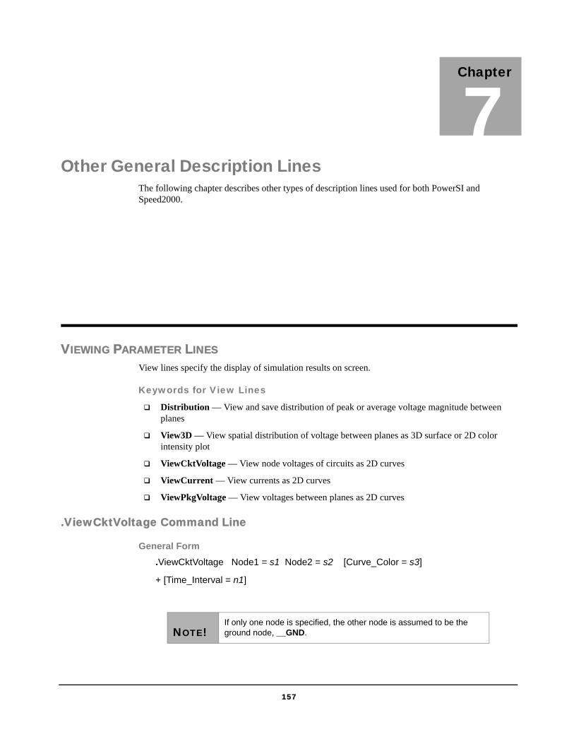
157
Chapter
7Other General Description Lines
The following chapter describes other types of description lines used for both PowerSI and Speed2000.
VIEWING PARAMETER LINESView lines specify the display of simulation results on screen.
Keywords for View Lines
Distribution — View and save distribution of peak or average voltage magnitude between planes
View3D — View spatial distribution of voltage between planes as 3D surface or 2D color intensity plot
ViewCktVoltage — View node voltages of circuits as 2D curves
ViewCurrent — View currents as 2D curves
ViewPkgVoltage — View voltages between planes as 2D curves
.ViewCktVoltage Command Line
General Form.ViewCktVoltage Node1 = s1 Node2 = s2 [Curve_Color = s3]
+ [Time_Interval = n1]
NOTE!If only one node is specified, the other node is assumed to be the ground node, __GND.

O T H E R G E N E R A L D E S C R I P T I O N L I N E S 1 5 8
Viewing Parameter Lines .spd File Format Reference Guide 11.1
ViewCktVoltage Parameter Descriptions
.ViewPkgVoltage Command Line
General Form for ViewPkgVoltage.ViewPkgVoltage PkgName.UpperLayerName_LowerLayerName
+ [Curve_Color = s1] Coord.x = f1 Coord.y = f2 [Time_Interval = n1]
ViewPkgVoltage Parameter Descriptions
PARAMETER EFFECT OR MEANING
.ViewCktVoltage Keyword for the .ViewCktVoltage line.
Node1 = s1
PartialCKT1Name.PartialCKT1DefName.Node1Name. The name of the node Node1Name in the partial circuit PartialCKT1Name, defined in ParticalCKT1DefName.
The voltage displayed is V(Node1)-V(Node2)
Node2 = s2
PartialCKT2Name.PartialCKT2DefName.Node2Name. The name of the node Node2Name in the partial circuit PartialCKT2Name, defined in ParticalCKT2DefName. Voltage displayed is V(Node1)-V(Node2)
Curve_Color = s3 s3 is the name of the color for displaying the curve. Default color: white.
Time_Interval = n1 Simulated result is displayed for every n1 time steps. Default value: 1.
PARAMETER EFFECT OR MEANING
.ViewPkgVoltage Keyword for .ViewPkgVoltage line.
Pkg-Name.UpperLayerName_LowerLayerName
The name of the upper layer and the name of the lower layer. Between these two layers, there is a voltage at a specified location displayed for the package named PkgName.
Curve_Color = s1 s1 is the name of the color for displaying the curve.Default: white.
Coord.x = f1 x coordinate of the output location.
Coord.y = f2 y coordinate of the output location.
Time_Interval = n1 Simulated result is displayed for every n1 time steps. Default value:1.

O T H E R G E N E R A L D E S C R I P T I O N L I N E S 1 5 9
Viewing Parameter Lines .spd File Format Reference Guide 11.1
.ViewCurrent Command Line
General Form for ViewCurrent .ViewCurrent Element = s1 Polarity = s2 [Curve_Color = s3]
+ [Time_Interval = n1]
ViewCurrent Parameter Descriptions
.View3D Command Line
General Form.View3D PkgName.UpperLayerName_LowerLayerName [Color_Intensity = YES(NO)]
+ [Mesh_Color = s1] [Frame_Color = s2] [Vmin = f1] Vmax = f2
+ [Space_Interval = n1] [Time_Interval = n2]
PARAMETER EFFECT OR MEANING
.ViewCurrent Keyword for .ViewCurrent line.
Element = s1
PartialCKTName.PartialCKTDefName.ElementName. The name of the element ElementName in the partial circuit PartialCKTName, defined in ParticalCKTDefName.PackageName.ElementName
The name of the element ElementName in the package PackageName”For Transmission Lines: -> Port1 or -> Port2 could be appended to ElementName to specify current at port 1 or port 2. Default: ->Port1.
For Traces: ->Nodename could be appended to ElementName to specify a node of the two terminal nodes.
Default: ->TraceStartingNodeName.
Polarity=s2s2 : + or - +: current from the positive node to the negative node.-: current from the negative node to the positive node.
Curve_Color = s3 s3 is the name of the color for displaying the curve. Default color: white.
Time_Interval = n1 Simulated result is displayed for every n1 time steps. Default value: 1.

O T H E R G E N E R A L D E S C R I P T I O N L I N E S 1 6 0
Viewing Parameter Lines .spd File Format Reference Guide 11.1
View3D Parameter Descriptions
PARAMETER EFFECT OR MEANING
.View3D Keyword for .View3D line.
PkgName.UpperLayerName_LowerLayerName
Name of the upper metal layer and the name of the lower metal layer.
Between these two layers there is a spatial distribution of voltage that is displayed for the package named PkgName
Color_Intensity= YESColor intensity plot for display.
Mesh_Color, Frame_Color, Vmin and Vmax are for 3D surface plot and have no effects if YES is specified.
Color_Intensity= NO 3D surface plot for display. Default.
Mesh_Color = s1 s1 is the name of the color for displaying the mesh.Default color: white.
Frame_Color = s2 s2 is the name of the color for displaying the frame of the mesh. Default color: white.
Vmin = f1
Numerical value which is mapped to the black color, for the minimum value, in the color intensity plot when
Color_Intensity = YES.Default value: -0.001.
Vmax = f2
Numerical value which is mapped to the red color, for the maximum value, in the color intensity plot when
Color_Intensity = YES. Default value: no default value. If Vmax isn’t specified, then SPD.
Space_Interval = n1 Simulated result is displayed for every n1 space steps. Default value: 1.
Time_Interval = n2 Simulated result is displayed for every n2 time steps. Default value: 1.

O T H E R G E N E R A L D E S C R I P T I O N L I N E S 1 6 1
Output Parameter Lines .spd File Format Reference Guide 11.1
.Distribution Command Line
General Form.Distribution PkgName.UpperLayerName_LowerLayerName
+ [Amplitude Peak(Average)] File_Name = s2
Distribution Parameter Descriptions
OUTPUT PARAMETER LINESThe data for spatial distribution of voltages between metal planes, and spatial distribution of parallel-mode currents on the plane surfaces (UP, DOWN or combined) can be stored in data files.
The .Output3DVoltage and .Output3DCurrent description lines need to be manually inserted into the corresponding .spd file at this moment.
.Output3DVoltage Command Line This command will generate a data file containing voltage distribution between planes. The position of the command line is after the .View3D command lines.
General Form.Output3DVoltage PkgName.UpperLayerName_LowerLayerName
+ [Space_Interval=n1] [Time_Inteval=n2] File_Name=s1 [DC=YES]
PARAMETER EFFECT OR MEANING
.Distribution Keyword for .Distribution line.
PkgName. UpperLayerName_LowerLayerName
Name of the upper metal layer and the name of the lower metal layer. Between these two layers there is the peak or the average value of voltage distribution that is saved for the package named by Pkg-Name.
Amplitude = Peak Store the peak amplitude of the voltage distribution in file s2;
Amplitude=Average Store the average amplitude of the voltage distribution in file s2.
File_Name = s2 A character string for the name of the output file.
IMPORTANT!! Use these two commands with caution. The output data file may be quite large.
NOTE!Time_Interval = LAST is acceptable, which means only output the volt-age at the last time step of simulation.

O T H E R G E N E R A L D E S C R I P T I O N L I N E S 1 6 2
Output Parameter Lines .spd File Format Reference Guide 11.1
Output3DVoltage Parameter Descriptions
.Output3DCurrent Command LineThis command generates the parallel-plate mode surface or total current of planes and patches. Three output data files are generated: Ix, Iy and Im.
Ix and Iy are the vector currents in X-direction and Y-direction.
Im is the magnitude of the currents and equals SQRT(Ix2+Iy2).
The Output3DCurrent command line is located after the .Output3DVoltage command lines.
General Form.Output3DCurrent PkgName.LayerName [Surface= s1]
+ [Space_Interval=n1] [Time_Interval=n2] File_Name=s2
Output3D Current Example 1This example specifies the output of the time varying current on the UP surface ofPlane02.
.Output3DCurrent Package1.Plane02 Surface = UP+ file_name = output_current.dat+ time_interval = 3 space_interval = 4
PARAMETER EFFECT OR MEANING
.Output3DVoltage Keyword for .Output3DVoltage line.
PkgName. UpperLayerName_LowerLayerName
Name of the upper metal layer and the name of the lower metal layer. Between these layers the spatial distribution of voltage is displayed for the package named PkgName.
Space_Interval = n1 Simulated result is saved for every n1 space steps. Default: 1.
Time_Interval = n2 Simulated result is saved for every n2 time steps. Default: 1.
File_Name = s1 A character string for the name of the output file.
DC Optional Parameter for Speed2000 only
DC = YESOutput voltage is the summation of the transient and DC.SPDSIM does not output fixed DC voltages in the Output3D data file.
DC = NO Output voltage does not contain the DC component, only transient results.
NOTENote
Time_Interval=LAST is acceptable, which means only output the cur-rent at the last time step of simulation.
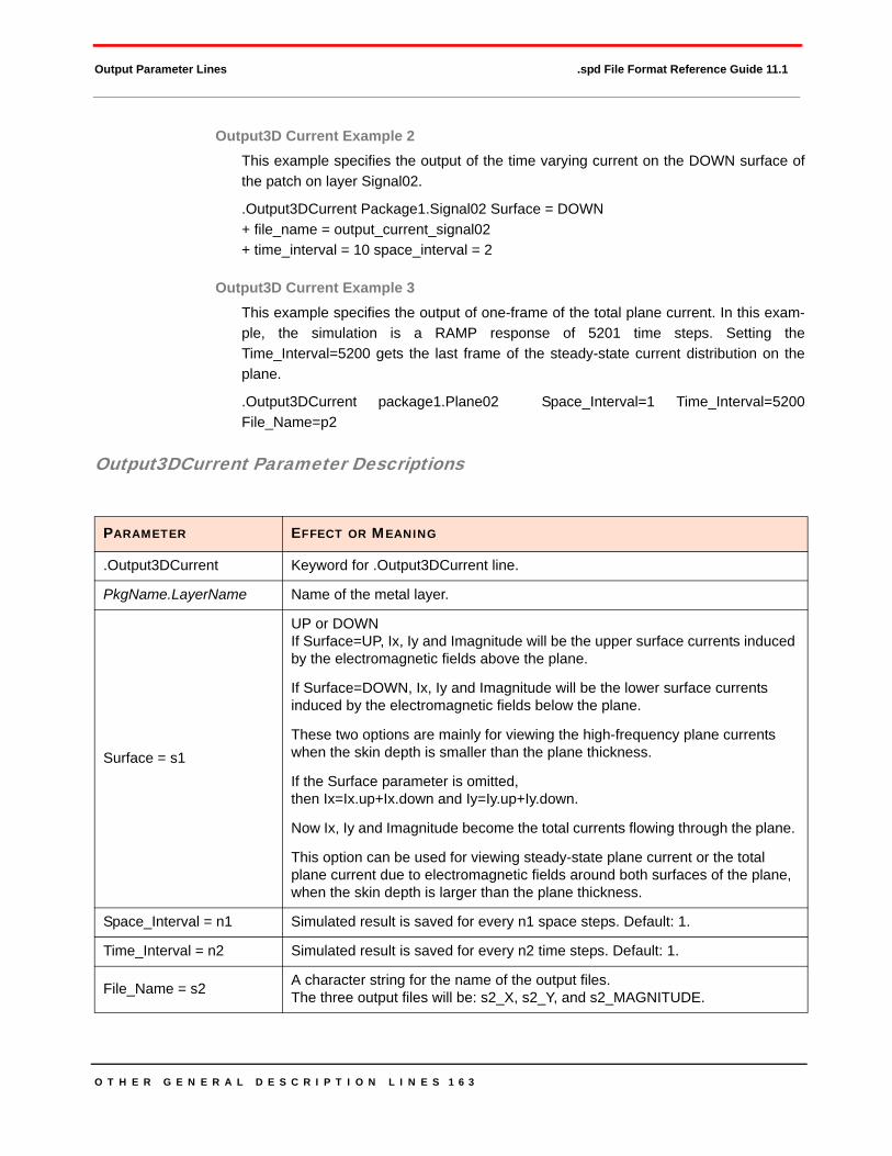
O T H E R G E N E R A L D E S C R I P T I O N L I N E S 1 6 3
Output Parameter Lines .spd File Format Reference Guide 11.1
Output3D Current Example 2This example specifies the output of the time varying current on the DOWN surface ofthe patch on layer Signal02.
.Output3DCurrent Package1.Signal02 Surface = DOWN+ file_name = output_current_signal02+ time_interval = 10 space_interval = 2
Output3D Current Example 3This example specifies the output of one-frame of the total plane current. In this exam-ple, the simulation is a RAMP response of 5201 time steps. Setting theTime_Interval=5200 gets the last frame of the steady-state current distribution on theplane.
.Output3DCurrent package1.Plane02 Space_Interval=1 Time_Interval=5200File_Name=p2
Output3DCurrent Parameter Descriptions
PARAMETER EFFECT OR MEANING
.Output3DCurrent Keyword for .Output3DCurrent line.
PkgName.LayerName Name of the metal layer.
Surface = s1
UP or DOWNIf Surface=UP, Ix, Iy and Imagnitude will be the upper surface currents induced by the electromagnetic fields above the plane.
If Surface=DOWN, Ix, Iy and Imagnitude will be the lower surface currents induced by the electromagnetic fields below the plane.
These two options are mainly for viewing the high-frequency plane currents when the skin depth is smaller than the plane thickness.
If the Surface parameter is omitted, then Ix=Ix.up+Ix.down and Iy=Iy.up+Iy.down.
Now Ix, Iy and Imagnitude become the total currents flowing through the plane.
This option can be used for viewing steady-state plane current or the total plane current due to electromagnetic fields around both surfaces of the plane, when the skin depth is larger than the plane thickness.
Space_Interval = n1 Simulated result is saved for every n1 space steps. Default: 1.
Time_Interval = n2 Simulated result is saved for every n2 time steps. Default: 1.
File_Name = s2 A character string for the name of the output files. The three output files will be: s2_X, s2_Y, and s2_MAGNITUDE.

O T H E R G E N E R A L D E S C R I P T I O N L I N E S 1 6 4
Net Management Lines .spd File Format Reference Guide 11.1
NET MANAGEMENT LINESWithin SPDGEN and PowerSI nets can be conveniently selected for simulation. These statements de-limit the Net Management section of the .spd file.
NetList StatementThe parameters of the .NetList statement are defined in this section.
.NetList
.EndNetList
General Form.NetList [Name1 [ {->| } [Name2] ] ] [::{Unselected|BranchUnselected} RiseTime=r1 + %Cou-pling=c1]
NetList Parameter Descriptions
PARAMETER EFFECT OR MEANING
Name1 Denotes a net or class or electrical net name. Name1 may not be present. Unnamed net includes all the elements that do not belong to any named net.
Name2
Specifies a class or electrical net to which Name1 belongs to establish a hierarchy. If Name2 is missing, Name1 belongs to the last occurrence of Name2. If there is no last occurrence of Name2, then Name1 does not belong to any other class.
->
Optional arrow symbol minus character + greater than character = arrow. If arrow present, it means Name1 belongs to the class specified by Name2. Name2 may not be present; in which case the value becomes the previous last occurrence of Name2.
This symbol is implemented so that in printed NetLists, perhaps containing thou-sands of members, the hierarchy is clear upon visual inspection. If arrow is missing, it means Name1 belongs to the same class as Name2 in the previous line.
::UnselectedIndicates that the specific item (class or net) denoted by Name1 is not selected for simulation. If the parameter ::Unselected appears at the beginning of a net listing, it means the unnamed net is not selected for simulation.
::BranchUnselected Indicates that this specific item denoted by Name1 and its children (if there are any) are not selected for simulation.
RiseTime = r1 Indicates that the net or class name has been selected for auto-coupled line calcula-tion. Value must be in ps.
%Coupling = c1 Indicates the net or class name has been selected for auto-coupled line calculation.
.INC Include another file into the current file.
.LIB Read libraries of commonly-used commands, device models, sub-circuits and partial circuits in library files.
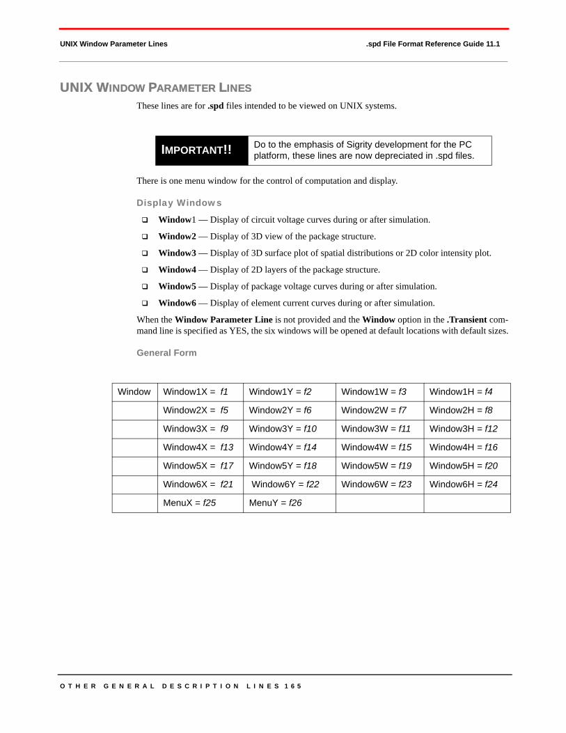
O T H E R G E N E R A L D E S C R I P T I O N L I N E S 1 6 5
UNIX Window Parameter Lines .spd File Format Reference Guide 11.1
UNIX WINDOW PARAMETER LINESThese lines are for .spd files intended to be viewed on UNIX systems.
There is one menu window for the control of computation and display.
Display Windows
Window1 — Display of circuit voltage curves during or after simulation.
Window2 — Display of 3D view of the package structure.
Window3 — Display of 3D surface plot of spatial distributions or 2D color intensity plot.
Window4 — Display of 2D layers of the package structure.
Window5 — Display of package voltage curves during or after simulation.
Window6 — Display of element current curves during or after simulation.
When the Window Parameter Line is not provided and the Window option in the .Transient com-mand line is specified as YES, the six windows will be opened at default locations with default sizes.
General Form
IMPORTANT!! Do to the emphasis of Sigrity development for the PC platform, these lines are now depreciated in .spd files.
Window Window1X = f1 Window1Y = f2 Window1W = f3 Window1H = f4
Window2X = f5 Window2Y = f6 Window2W = f7 Window2H = f8
Window3X = f9 Window3Y = f10 Window3W = f11 Window3H = f12
Window4X = f13 Window4Y = f14 Window4W = f15 Window4H = f16
Window5X = f17 Window5Y = f18 Window5W = f19 Window5H = f20
Window6X = f21 Window6Y = f22 Window6W = f23 Window6H = f24
MenuX = f25 MenuY = f26
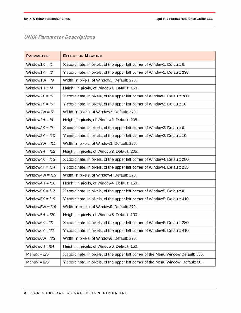
O T H E R G E N E R A L D E S C R I P T I O N L I N E S 1 6 6
UNIX Window Parameter Lines .spd File Format Reference Guide 11.1
UNIX Parameter Descriptions
PARAMETER EFFECT OR MEANING
Window1X = f1 X coordinate, in pixels, of the upper left corner of Window1. Default: 0.
Window1Y = f2 Y coordinate, in pixels, of the upper left corner of Window1. Default: 235.
Window1W = f3 Width, in pixels, of Window1. Default: 270.
Window1H = f4 Height, in pixels, of Window1. Default: 150.
Window2X = f5 X coordinate, in pixels, of the upper left corner of Window2. Default: 280.
Window2Y = f6 Y coordinate, in pixels, of the upper left corner of Window2. Default: 10.
Window2W = f7 Width, in pixels, of Window2. Default: 270.
Window2H = f8 Height, in pixels, of Window2. Default: 205.
Window3X = f9 X coordinate, in pixels, of the upper left corner of Window3. Default: 0.
Window3Y = f10 Y coordinate, in pixels, of the upper left corner of Window3. Default: 10.
Window3W = f11 Width, in pixels, of Window3. Default: 270.
Window3H = f12 Height, in pixels, of Window3. Default: 205.
Window4X = f13 X coordinate, in pixels, of the upper left corner of Window4. Default: 280.
Window4Y = f14 Y coordinate, in pixels, of the upper left corner of Window4. Default: 235.
Window4W = f15 Width, in pixels, of Window4. Default: 270.
Window4H = f16 Height, in pixels, of Window4. Default: 150.
Window5X = f17 X coordinate, in pixels, of the upper left corner of Window5. Default: 0.
Window5Y = f18 Y coordinate, in pixels, of the upper left corner of Window5. Default: 410.
Window5W = f19 Width, in pixels, of Window5. Default: 270.
Window5H = f20 Height, in pixels, of Window5. Default: 100.
Window6X =f21 X coordinate, in pixels, of the upper left corner of Window6. Default: 280.
Window6Y =f22 Y coordinate, in pixels, of the upper left corner of Window6. Default: 410.
Window6W =f23 Width, in pixels, of Window6. Default: 270.
Window6H =f24 Height, in pixels, of Window6. Default: 150.
MenuX = f25 X coordinate, in pixels, of the upper left corner of the Menu Window Default: 565.
MenuY = f26 Y coordinate, in pixels, of the upper left corner of the Menu Window. Default: 30.
167
Chapter
8PowerSI Formats
This chapter describes some of the .spd file formats used for PowerSI only, in addition to the ones used for both PowerSI and Speed2000.
S-ELEMENTThe S-Element is used strictly for including an S-Element in the Sigrity PowerSI application. It provides a convenient way to incorporate:
• A multi-terminal or multi-port network.
• Subsystems into a package.
• A board for simulation.
The S-Element is characterized by its frequency-dependent multi-port network parameters including:
• Admittance parameter (Y-parameter)• Impedance parameter (Z-parameter)• Scattering parameter (S-parameter)
General FormSxxx {nd1 nd2 ... ndN ndRef | nd1 ndRef1 nd2 ndRef2... ndN ndRef}+ {MNAME=Smodel_name | model=data_file}
S-Element ExampleS1234 DieVCC DieGnd BrdVCC BrdGnd Model=”packagepgmodel.s2p”
S1234 DieVCC DieGnd BrdVCC BrdGnd mname=s_model
P O W E R S I F O R M A T S 1 6 8
.PowerSI Commands .spd File Format Reference Guide 11.1
S - Element Parameter Descriptions
.POWERSI COMMANDS
General Form for PowerSI .PowerSI
General Form for .EndPowerSI .EndPowerSI
SOURCE TYPESIn PowerSI you cannot use periodic and non-periodic sources at the same time.
Random BitsPowerSI does not accept the Random_Bit source. If you put the initial value on a new line, it works correctly, as shown in the example below.
V_in Out Nvss RANDOM_BIT (
+ 0 0.5 DATA_RATE=5G POLY=23
+ TR=0.01n TF=0.01n JITTER=0.2 NOISE=0.05)
If everything is typed on one line or the first parameter on the line with the source name, then the source will not be accepted. The following example shows how a single line will not work.
V_in Out Nvss RANDOM_BIT (0 0.5 DATA_RATE=5G POLY=23 TR=0.01n TF=0.01n
JITTER=0.2 NOISE=0.05)
Source NetlistsThe latest version of PowerSI doesn't accept any Random Bit source netlist. Check:
• Random_Bit keyword can be supported.
• Netlist forms stated so they are correctly interpreted by the parser.
PARAMETER EFFECT OR MEANING
Sxxx A character string, starting with S, for the name of an S-Element.
nd1 nd2 ... ndN ndRef Node names. nd1 nd2 ... ndN: Port nodes. ndRef: Reference node.
nd1 ndRef1 nd2 ndRef2. Node names. nd1 nd2 ... ndN: Port nodes. ndRef1.
ndN ndRef ndref2...ndRef: Reference nodes.
model BNP or Touchstone file name.
mname Name of S model; defined in .model description lines.

P O W E R S I F O R M A T S 1 6 9
Section Lines .spd File Format Reference Guide 11.1
SECTION LINESPowerSI section lines specify parameters that are unique to PowerSI. The PowerSI section begins with .PowerSI and ends with .EndPowerSI.
P O W E R S I F O R M A T S 1 7 0
Section Lines .spd File Format Reference Guide 11.1
.FrequencySweepThe .FrequencySweep line specifies frequency simulation parameters, such as:
• Starting and ending frequency• Frequency increment for linear type sweeping• Maximum sampling frequencies for the adaptive type sweeping
General Form.FrequencySweep dStartingFrequency dEndingFrequency + {dIncrement | nPointsPerDecade | nMaxSamples} + [{Linear | Log | Adaptive}]
...
.FrequencySweep dStartingFrequency dEndingFrequency + {dIncrement | nPointsPerDecade | nMaxSamples} + [{Linear | Log | Adaptive}]
Frequency Sweep Example 1This sample defines the sweeping scheme as linear, starting from 10MHz going to2GHz, stepping by 20MHz.
.FrequencySweep 10MHz 2GHz 20MHz Linear
Frequency Sweep Example 2This sample defines the sweeping scheme as adaptive, starting from 10MHz going to2GHz, with a maximum of 30 samples.
.FrequencySweep 10MHz 2GHz 30 Adaptive
P O W E R S I F O R M A T S 1 7 1
Section Lines .spd File Format Reference Guide 11.1
FrequencySweep Parameter Descriptions
PARAMETER EFFECT OR MEANING
.FrequencySweep Keyword for frequency sweeping parameters line.
dStartingFrequency Starting frequency. Default = 10MHz.
dEndingFrequency Ending frequency. Default = 2GHz.
dIncrement Frequency increment for linear sweeping. Default = 10MHz.
nPointsPerDecade Number of points per decade.
nMaxSamples Max samples for adaptive sweeping. Default = 40 * integer [(dEndingFrequency - dStartingFrequency) / 2GHz] + 40
Linear Linear sweeping.
Log Logarithmic sweeping.
Adaptive Adaptive sweeping. Default = Linear.

P O W E R S I F O R M A T S 1 7 2
.Port Commands .spd File Format Reference Guide 11.1
.PORT COMMANDSPorts are defined between the .Port and .EndPort command lines. A unique port statement, Portxxxx, is inserted to define each port. Each port has a positive terminal and a negative terminal.
General Form for PortxxxxPortxxxx + PositiveTerminal [PkgNodeName [ PkgNodeName]…]+ NegativeTerminal [PkgNodeName [ PkgNodeName]…]
Portxxxx Example 1 - One Port Defined.PortPort0001+ PositiveTerminal $Package.Node94::VCC+ NegativeTerminal $Package.Node302::GND.EndPort
Portxxxx Example 2 - Multiple Ports Defined.PowerSI.FrequencySweep 1.000000e+001MHz 2.000000e+000GHz 40 Adaptive.PortPort1+ PositiveTerminal Package1.Node09+ NegativeTerminal Package1.Node029Port2+ PositiveTerminal Package1.Node010+ NegativeTerminal Package1.Node031Port3+ PositiveTerminal Package1.Node011+ NegativeTerminal Package1.Node033Port4+ PositiveTerminal Package1.Node012+ NegativeTerminal Package1.Node035.EndPort.EndPowerSI
Portxxxx Parameter Descriptions
PARAMETER EFFECT OR MEANING
Portxxxx A character string, starting with Port, for the name of the port.
PkgNodeName Names of the package nodes. Define the positive and negative terminals of the port.
P O W E R S I F O R M A T S 1 7 3
.DiffChannels Commands .spd File Format Reference Guide 11.1
.DIFFCHANNELS COMMANDSDifferential channel ports are defined between the .DiffChannels and .EndDiffChannels command lines. A unique differential channel statement, Diff_Channel_xxxx_$_yyyy, is inserted to define a dif-ferential channel setting.
This section follows the .NetList section in the .spd file.
General Form for Diff_Channel_xxxx_$_yyyDiff_Channel_xxxx_$_yyyy
+ “xxxx” “yyyy”
+ [ “PortName1” “PortName2” [“PortName1” “PortName2”] ... ]
Diff_Channel_xxxx_$_yyyy Example.DiffChannels
Diff_Channel_IO_L26P_10_$_10_L29N_10_”IP_L26P_10” “IO_L29N_10”
+ Port1_D1_922::IO_L26P_10”
+ Port2_D1_936::IO_L29N_10”
+ Port3_B1_T4::IO_L26P_10”
+ Port4_B1_U4::IO_L29N_10”
.EndDiffChannels
Diff_Channel_xxxx_$_yyyy Parameter Descriptions
Parameter Meaning
xxxx Net 1
yyyy Net 2 (Net1 and Net2 composed of a differential net pair, seen in Net Man-ager with a tie sign.)
PortName1 Name of port in Net 1
PortName2
Name of port in Net 2 (PortName1 and PortName2 compose of differen-tial channel port pair. These ports can be observed in the ‘Diff Channel Ports’ dialog in the Port dialog.)
NOTE! A differential channel can contain one or more than one port pair.
The port (in Net1 or Net2) of pair must exist and be enabled.
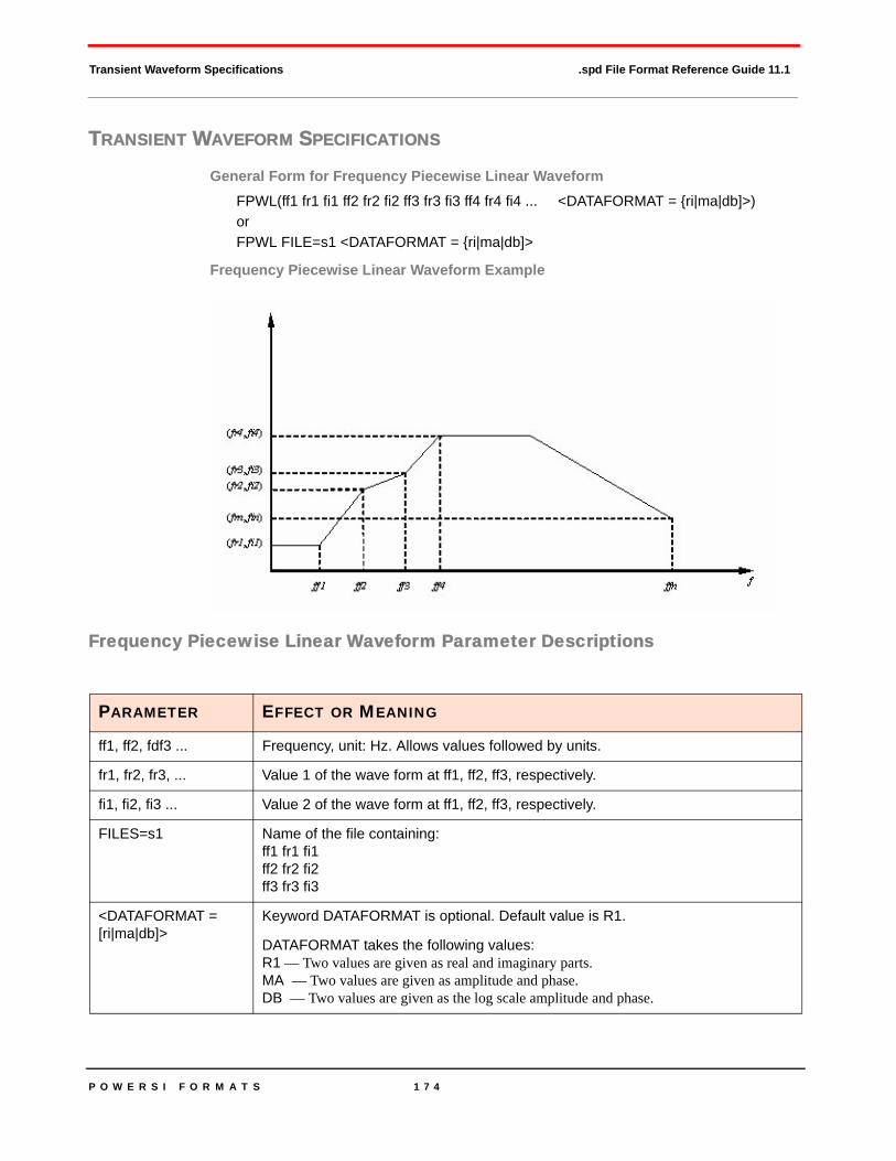
P O W E R S I F O R M A T S 1 7 4
Transient Waveform Specifications .spd File Format Reference Guide 11.1
TRANSIENT WAVEFORM SPECIFICATIONS
General Form for Frequency Piecewise Linear WaveformFPWL(ff1 fr1 fi1 ff2 fr2 fi2 ff3 fr3 fi3 ff4 fr4 fi4 ... <DATAFORMAT = {ri|ma|db]>)orFPWL FILE=s1 <DATAFORMAT = {ri|ma|db]>
Frequency Piecewise Linear Waveform Example
Frequency Piecewise Linear Waveform Parameter Descriptions
PARAMETER EFFECT OR MEANING
ff1, ff2, fdf3 ... Frequency, unit: Hz. Allows values followed by units.
fr1, fr2, fr3, ... Value 1 of the wave form at ff1, ff2, ff3, respectively.
fi1, fi2, fi3 ... Value 2 of the wave form at ff1, ff2, ff3, respectively.
FILES=s1 Name of the file containing:ff1 fr1 fi1ff2 fr2 fi2ff3 fr3 fi3
<DATAFORMAT = [ri|ma|db]>
Keyword DATAFORMAT is optional. Default value is R1.
DATAFORMAT takes the following values:R1 — Two values are given as real and imaginary parts.MA — Two values are given as amplitude and phase.DB — Two values are given as the log scale amplitude and phase.
175
Chapter
9Speed2000 Format
This chapter describes the spd file format strictly used by Speed2000 in addition to the more common formats used by both Speed2000 and PowerSI.
SPEED2000 COMMANDSGeneral Form for SPEED2000
.SPEED2000
General Form for .EndSPEED2000
.EndSPEED2000
Examples
TDR/TDT mode.SPEED2000
.Mode = TDR/TDT
.TDR TDRport1 True TDTport1
.TDR TDRport2 True TDTport2
.
.
.
.TDR TDRportn True TDTportn
.EndSPEED2000

S P E E D 2 0 0 0 F O R M A T 1 7 6
SPEED2000 COMMANDS .spd File Format Reference Guide 11.1
SSO checking mode.SPEED2000
.Mode = SSO
.SSO NEXTport1 FEXTport1 Enable=YES
.SSO NEXTport2 FEXTport2 Enable=YES
.
.
.
.SSO NEXTportn FEXTportn Enable=YES
.EndSPEED2000
Description Lines
.Mode description lineThis Mode description line specifies the simulation mode of SPEED2000.
General Form .mode = mode_name
Mode Line Parameter Descriptions
.TDR description line This TDR description line specifies the TDR and TDT ports in TDR / TDT mode.
General Form .TDR TDRport usage TDTport
TDR Line Parameter Descriptions
PARAMETER EFFECT OR MEANING
mode_name Simulation mode name, can be SSO or TDR/TDT.
PARAMETER EFFECT OR MEANING
TDRport TDR port name.
TDTport TDT port name.
usage Flag indicates whether this TDR line is used for simulation. When usage = TRUE, this line is used. When usage = False, it is not used.

S P E E D 2 0 0 0 F O R M A T 1 7 7
I/O Buffer Information Specification (IBIS) .spd File Format Reference Guide 11.1
.SSO description line This SSO description line specifies the SSO ports in SSO checking modes.
General Form.SSO NEXTport FEXTport Enable = usage
SSO Line Parameter Descriptions
I/O BUFFER INFORMATION SPECIFICATION (IBIS) SPEED2000 can read in and simulate IBIS models. This section describes the file format for the IBIS standard (version 5.0) buffers.
Related Topics
• To review the IBIS specification refer to:
http://www.eigroup.org (maintained by the IBIS committee)
• Pointers to IBIS models of different IC manufacturers can be found at the following sites:
http://www.eigroup.org/IBIS/ibis%20table/models.htm
This site is maintained by the IBIS committee.
http://www.mentor.com/icx/modeling/ibis_modeling.html#manufacturer
This site is maintained by Mentor Graphics.
PARAMETER EFFECT OR MEANING
NEXTport Near End Cross Talk port name.
FEXTport Far End Cross Talk port name.
usageFlag indicates whether this SSO line is used for simulation. When usage = YES, this line is used. When usage = NO, it is not used.

S P E E D 2 0 0 0 F O R M A T 1 7 8
I/O Buffer Information Specification (IBIS) .spd File Format Reference Guide 11.1
Supported KeywordsSPDSIM currently parses the following data sections for an IBIS file:
[Bandwidth] [Model] [Pullup Reference]
[Cac] [Model Data] [Rac]
[C Series] [Model Selector] [Ramp]
[Capacitance Matrix] [Number Of Pins] [Rc Series][Series Current]
[Component] [Number Of Sections] [Resistance Matrix]
[Driver Schedule] [Off] [Rgnd]
[Define Package Model] [On] [Rising Waveform]
[End Package Model] [Package] [RI Series]
[End] [Package Model] [Row]
[End Model Data] [Pin] [Rpower]
[Falling Waveform] [Pin Mapping] [R Series]
[GND_Clamp] [Pin Numbers] [Series MOSFET]
[GND Clamp Reference] [POWER Clamp] [Series Pin Mapping]
[GND Pulse Table] [POWER Clamp Reference] [Series Switch Groups]
[Inductance Matrix] [POWER Pulse Table] [Submodel]
[Lc Series] [Pulldown] [Submodel Spec]
[L Series] [Pulldown Reference] [Voltage Range]
[Manufacturer] [Compost Current] [ISSO PU]
[ISSO PD]

S P E E D 2 0 0 0 F O R M A T 1 7 9
I/O Buffer Information Specification (IBIS) .spd File Format Reference Guide 11.1
Random BitsSPEED2000 doesn't accept the Random_Bit source.
Put the initial value on a new line.
V_in Out Nvss RANDOM_BIT (
+ 0 0.5 DATA_RATE=5G POLY=23
+ TR=0.01n TF=0.01n JITTER=0.2 NOISE=0.05)
If everything is typed on one line or the first parameter on the line with the source name then the source will not be accepted.
The following example shows how a single line will not work.
V_in Out Nvss RANDOM_BIT (0 0.5 DATA_RATE=5G POLY=23 TR=0.01n TF=0.01n
JITTER=0.2 NOISE=0.05)
Source NetlistsThe latest SPEED2000 doesn't accept any Random Bit source netlist. You should check:
Netlist forms stated so they are correctly interpreted by the parser
Random_Bit keyword can be supported
IBIS Statements
General FormBxxxx node1 node2 ...
+ file=file_name model=model_name
+ [typ={typ|min|max|fast|slow}]
+ [buffer=type of IBIS buffer]
+ [ramp_fwf={0|1|2}]
+ [ramp_rwf={0|1|2}]
+ [c_com_pu=c_com_pu_value]
+ [c_com_pd=c_com_pd_value]
+ [c_com_pc=c_com_pc_value]
+ [c_com_gc=c_com_gc_value]
+ [pkgfile=pkgfile_name]
+ [package={yes|model|no}]
+ [component=component_name]
+ [pin=pin_name]
+ [power={on|off}]
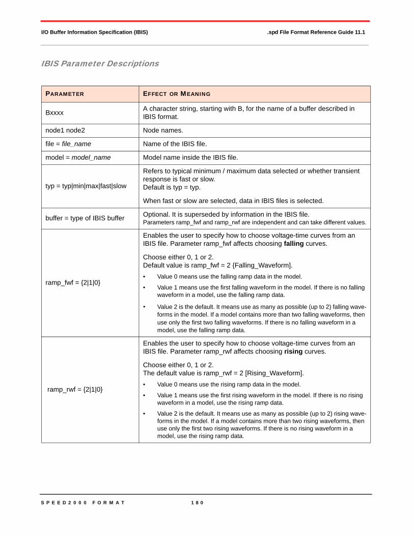
S P E E D 2 0 0 0 F O R M A T 1 8 0
I/O Buffer Information Specification (IBIS) .spd File Format Reference Guide 11.1
IBIS Parameter Descriptions
PARAMETER EFFECT OR MEANING
Bxxxx A character string, starting with B, for the name of a buffer described in IBIS format.
node1 node2 Node names.
file = file_name Name of the IBIS file.
model = model_name Model name inside the IBIS file.
typ = typ|min|max|fast|slow
Refers to typical minimum / maximum data selected or whether transient response is fast or slow. Default is typ = typ.
When fast or slow are selected, data in IBIS files is selected.
buffer = type of IBIS buffer Optional. It is superseded by information in the IBIS file.Parameters ramp_fwf and ramp_rwf are independent and can take different values.
ramp_fwf = {2|1|0}
Enables the user to specify how to choose voltage-time curves from an IBIS file. Parameter ramp_fwf affects choosing falling curves.
Choose either 0, 1 or 2. Default value is ramp_fwf = 2 {Falling_Waveform]. • Value 0 means use the falling ramp data in the model.
• Value 1 means use the first falling waveform in the model. If there is no falling waveform in a model, use the falling ramp data.
• Value 2 is the default. It means use as many as possible (up to 2) falling wave-forms in the model. If a model contains more than two falling waveforms, then use only the first two falling waveforms. If there is no falling waveform in a model, use the falling ramp data.
ramp_rwf = {2|1|0}
Enables the user to specify how to choose voltage-time curves from an IBIS file. Parameter ramp_rwf affects choosing rising curves.
Choose either 0, 1 or 2. The default value is ramp_rwf = 2 [Rising_Waveform]. • Value 0 means use the rising ramp data in the model.
• Value 1 means use the first rising waveform in the model. If there is no rising waveform in a model, use the rising ramp data.
• Value 2 is the default. It means use as many as possible (up to 2) rising wave-forms in the model. If a model contains more than two rising waveforms, then use only the first two rising waveforms. If there is no rising waveform in a model, use the rising ramp data.
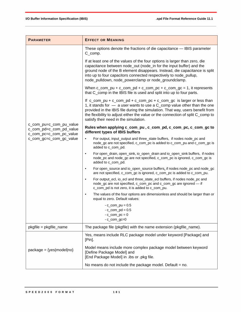
S P E E D 2 0 0 0 F O R M A T 1 8 1
I/O Buffer Information Specification (IBIS) .spd File Format Reference Guide 11.1
c_com_pu=c_com_pu_valuec_com_pd=c_com_pd_valuec_com_pc=c_com_pc_valuec_com_gc=c_com_gc_value
These options denote the fractions of die capacitance — IBIS parameter C_comp.
If at least one of the values of the four options is larger than zero, die capacitance between node_out (node_in for the input buffer) and the ground node of the B element disappears. Instead, die capacitance is split into up to four capacitors connected respectively to node_pullup, node_pulldown, node_powerclamp or node_groundclamp.
When c_com_pu + c_com_pd + c_com_pc + c_com_gc = 1, it represents that C_comp in the IBIS file is used and split into up to four parts.
If c_com_pu + c_com_pd + c_com_pc + c_com_gc is larger or less than 1, it stands for — a user wants to use a C_comp value other than the one provided in the IBIS file during the simulation. That way, users benefit from the flexibility to adjust either the value or the connection of split C_comp to satisfy their need in the simulation.
Rules when applying c_com_pu , c_com_pd, c_com_pc, c_com_gc to different types of IBIS buffers • For output, input_output and three_state buffers, if nodes node_pc and
node_gc are not specified, c_com_pc is added to c_com_pu and c_com_gc is added to c_com_pd.
• For open_drain, open_sink, io_open_drain and io_open_sink buffers, if nodes node_pc and node_gc are not specified, c_com_pc is ignored, c_com_gc is added to c_com_pd.
• For open_source and io_open_source buffers, if nodes node_pc and node_gc are not specified, c_com_gc is ignored, c_com_pc is added to c_com_pu.
• For output_ecl, io_ecl and three_state_ecl buffers, if nodes node_pc and node_gc are not specified, c_com_pc and c_com_gc are ignored — if c_com_pd is not zero, it is added to c_com_pu.
• The values of the four options are dimensionless and should be larger than or equal to zero. Default values:
- c_com_pu = 0.5- c_com_pd = 0.5- c_com_pc = 0- c_com_gc=0
pkgfile = pkgfile_name The package file (pkgfile) with the name extension (pkgfile_name).
package = {yes|model|no}
Yes, means include RLC package model under keyword [Package] and [Pin].
Model means include more complex package model between keyword [Define Package Model] and [End Package Model] in .ibs or .pkg file.
No means do not include the package model. Default = no.
PARAMETER EFFECT OR MEANING

S P E E D 2 0 0 0 F O R M A T 1 8 2
I/O Buffer Information Specification (IBIS) .spd File Format Reference Guide 11.1
IBIS Input Buffer
General Form Bxxxx nd_pc nd_gc nd_in gnd nd_out_of_in
+ file=’file_name’ model=’model_name’
+ [typ={typ|min|max|fast|slow}]
+ [buffer=input]
+ [c_com_pu=c_com_pu_value]
+ [c_com_pd=c_com_pd_value]
+ [c_com_pc=c_com_pc_value]
+ [c_com_gc=c_com_gc_value]
+ [pkgfile=pkgfile_name]
+ [package={yes|model|no}]
+ [component=component_name]
+ [pin=pin_name]
+ [power={on|off}]
component = component_namepin = pin_name
These two options are in effect only if package =YES.
When they are in effect, SPDSIM reads the package parameters (package R, L and C) from the specified component and pin section in an IBIS file, instead of from the package section.
These two parameters are always used together.
If package =YES, and either one of them or both is missing, then SPDSIM reads the first available package parameters in the package section(s) from an IBIS file.
These two parameters are useful when user wants to use the package parameters related to a special pin. Component parameter is also neces-sary because an IBIS file may contain several component definitions.
There is no default value for these two options.
power = {on|off}The flag for adding initial power for the IBIS buffer.
ON — Add the initial power.OFF — Do not add the initial power. Default value.
PARAMETER EFFECT OR MEANING

S P E E D 2 0 0 0 F O R M A T 1 8 3
I/O Buffer Information Specification (IBIS) .spd File Format Reference Guide 11.1
IBIS Input Buffer IllustrationThe components inside the box do not appear when package = no.
NOTE! The rule for determining buffer state is the same as Output Buffer.
nd_gc
nd_pc
Globalground
nd_out_of_in
V_out_of_in
PowerClamp
GNDClamp
nd_in0
+
-
+
-
INPUT Buffer
gnd
C_comp
gnd
C_pkg
L_pkgR_pkg nd_pin
V(t)

S P E E D 2 0 0 0 F O R M A T 1 8 4
I/O Buffer Information Specification (IBIS) .spd File Format Reference Guide 11.1
IBIS Input Buffer Parameter Descriptions
PARAMETER EFFECT OR MEANING
nd_pc Node of power clamp.
nd_gc Node of ground clamp.
nd_in Node of input, nd_in is nd_in0 above.
nd_pin Appears only when package=yes and it functions as nd_in.
gnd Ground node.
nd_out_of_in Node which is linked with the digital signal of input buffer.
V_out_of_in
Digital output signal (value = 0 or 1).
V_out_of_in signal value is determined by V_nd_in, Vinl, Vinh and Polarity.
Vinl, Vinh and Polarity values are given in the referenced IBIS file. • V_nd_in — Voltage of nd_in0 (or nd_in) relative to gnd
• Vinl — Input logic low DC voltage. Default value: 0.2V
• Vinh — Input logic high DC voltage. Default value: 0.8V
• Polarity — Model polarity. It has two values: Non-Inverting and Inverting.
Default value: Non-Inverting.
Rules for Determining the Value of V_out_of_in
At beginning of the transient simulation (t=0) or in DC analysis... when Polarity=Non-Inverting:
• V_out_of_in = 1 if V_nd_in>=(Vinh+Vinl)/2• V_out_of_in = 0 if V_nd_in<(Vinh+Vinl)/2
When Polarity= Inverting:• V_out_of_in = 0 if V_nd_in>=(Vinh+Vinl)/2• V_out_of_in = 1 if V_nd_in<(Vinh+Vinl)/2
During the transient simulation (t>0)... when Polarity=Non-Inverting:• V_out_of_in = 1 if V_nd_in>Vinh• V_out_of_in = 0 if V_nd_in<Vinl• V_out_of_in does not change value
if Vinl<=V_nd_in<=Vinh
When Polarity= Inverting: • V_out_of_in = 0 if V_nd_in>Vinh• V_out_of_in = 1 if V_nd_in<Vinl• V_out_of_in does not change value
if Vinl<=V_nd_in<=Vinh
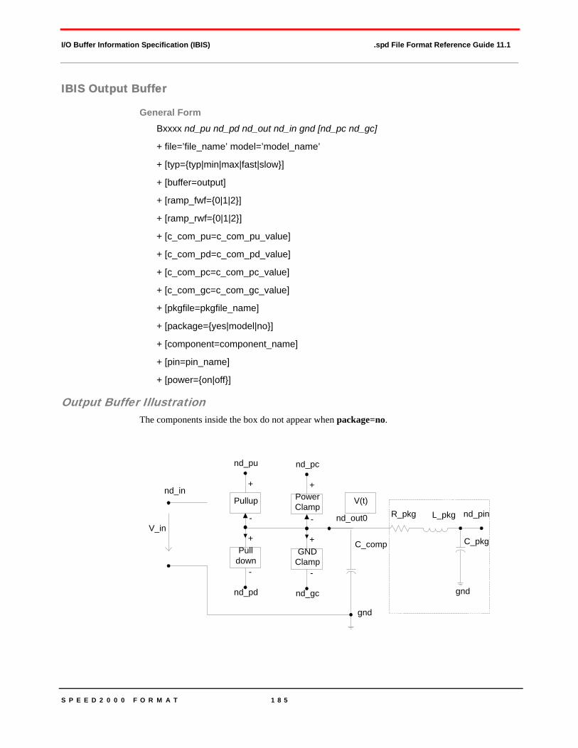
S P E E D 2 0 0 0 F O R M A T 1 8 5
I/O Buffer Information Specification (IBIS) .spd File Format Reference Guide 11.1
IBIS Output Buffer
General FormBxxxx nd_pu nd_pd nd_out nd_in gnd [nd_pc nd_gc]
+ file=’file_name’ model=’model_name’
+ [typ={typ|min|max|fast|slow}]
+ [buffer=output]
+ [ramp_fwf={0|1|2}]
+ [ramp_rwf={0|1|2}]
+ [c_com_pu=c_com_pu_value]
+ [c_com_pd=c_com_pd_value]
+ [c_com_pc=c_com_pc_value]
+ [c_com_gc=c_com_gc_value]
+ [pkgfile=pkgfile_name]
+ [package={yes|model|no}]
+ [component=component_name]
+ [pin=pin_name]
+ [power={on|off}]
Output Buffer IllustrationThe components inside the box do not appear when package=no.
nd_gc
nd_pc
gnd
C_comp
PowerClamp
GNDClamp
+
-
+
-
OUTPUT Buffer
nd_pd
nd_pu
Pullup
Pulldown
+
-
+
-
nd_in
gnd
C_pkg
L_pkgR_pkgV(t)
nd_pinnd_out0V_in
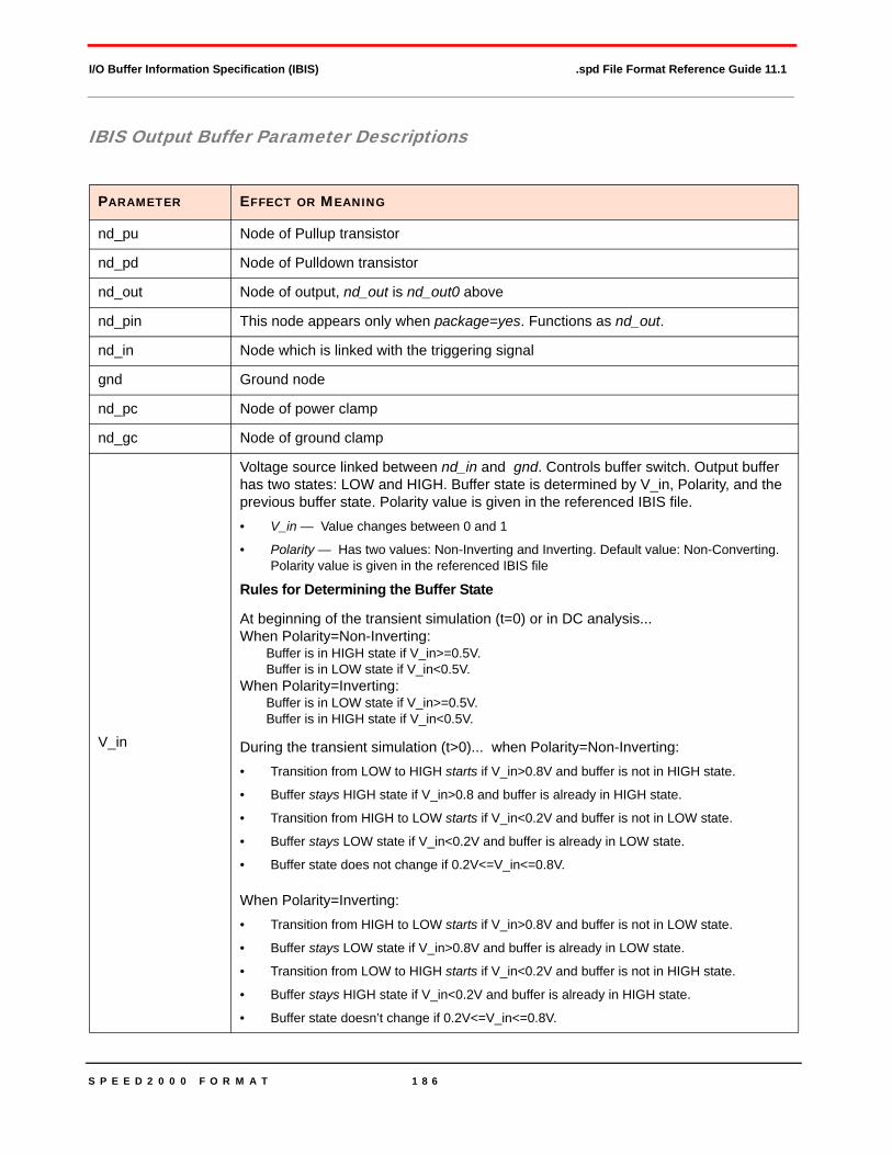
S P E E D 2 0 0 0 F O R M A T 1 8 6
I/O Buffer Information Specification (IBIS) .spd File Format Reference Guide 11.1
IBIS Output Buffer Parameter Descriptions
PARAMETER EFFECT OR MEANING
nd_pu Node of Pullup transistor
nd_pd Node of Pulldown transistor
nd_out Node of output, nd_out is nd_out0 above
nd_pin This node appears only when package=yes. Functions as nd_out.
nd_in Node which is linked with the triggering signal
gnd Ground node
nd_pc Node of power clamp
nd_gc Node of ground clamp
V_in
Voltage source linked between nd_in and gnd. Controls buffer switch. Output buffer has two states: LOW and HIGH. Buffer state is determined by V_in, Polarity, and the previous buffer state. Polarity value is given in the referenced IBIS file.• V_in — Value changes between 0 and 1
• Polarity — Has two values: Non-Inverting and Inverting. Default value: Non-Converting. Polarity value is given in the referenced IBIS file
Rules for Determining the Buffer State
At beginning of the transient simulation (t=0) or in DC analysis...When Polarity=Non-Inverting:
Buffer is in HIGH state if V_in>=0.5V.Buffer is in LOW state if V_in<0.5V.
When Polarity=Inverting:Buffer is in LOW state if V_in>=0.5V.Buffer is in HIGH state if V_in<0.5V.
During the transient simulation (t>0)... when Polarity=Non-Inverting:• Transition from LOW to HIGH starts if V_in>0.8V and buffer is not in HIGH state.
• Buffer stays HIGH state if V_in>0.8 and buffer is already in HIGH state.
• Transition from HIGH to LOW starts if V_in<0.2V and buffer is not in LOW state.
• Buffer stays LOW state if V_in<0.2V and buffer is already in LOW state.
• Buffer state does not change if 0.2V<=V_in<=0.8V.
When Polarity=Inverting:• Transition from HIGH to LOW starts if V_in>0.8V and buffer is not in LOW state.
• Buffer stays LOW state if V_in>0.8V and buffer is already in LOW state.
• Transition from LOW to HIGH starts if V_in<0.2V and buffer is not in HIGH state.
• Buffer stays HIGH state if V_in<0.2V and buffer is already in HIGH state.
• Buffer state doesn’t change if 0.2V<=V_in<=0.8V.

S P E E D 2 0 0 0 F O R M A T 1 8 7
I/O Buffer Information Specification (IBIS) .spd File Format Reference Guide 11.1
IBIS Tristate BufferThe Tristate buffer has two major states: ENABLE and DISABLE. The ENABLE state differentiates between HIGH and LOW. There are totally three states for tristate buffer: LOW, HIGH and DISABLE.
The buffer state is determined by: V_in, V_en, Polarity, Enable and the previous buffer state. Polarity and Enable values are given in the referenced IBIS file.
General FormBxxxx nd_pu nd_pd nd_out nd_in nd_en gnd [nd_pc nd_gc]
+ file=’file_name’ model=’model_name’
+ [typ={typ|min|max|fast|slow}]
+ [buffer=three_state]
+ [ramp_fwf={0|1|2}]
+ [ramp_rwf={0|1|2}]
+ [c_com_pu=c_com_pu_value]
+ [c_com_pd=c_com_pd_value]
+ [c_com_pc=c_com_pc_value]
+ [c_com_gc=c_com_gc_value]
+ [pkgfile=pkgfile_name]
+ [package={yes|model|no}] default=no
+ [component=component_name]
+ [pin=pin_name]
+ [power={on|off}]
IBIS Tristate Buffer IllustrationThe components inside the box do not appear when package=no.
nd_gc
nd_pc
gnd
C_comp
PowerClamp
GNDClamp
+
-
+
-
3-STATE Buffer
nd_pd
nd_pu
Pullup
Pulldown
+
-
+
-
gnd
C_pkg
L_pkgR_pkgV(t)
nd_pinnd_out0
nd_in
V_in
nd_en
V_en
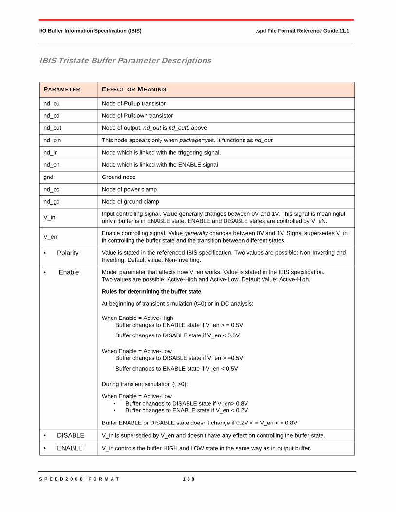
S P E E D 2 0 0 0 F O R M A T 1 8 8
I/O Buffer Information Specification (IBIS) .spd File Format Reference Guide 11.1
IBIS Tristate Buffer Parameter Descriptions
PARAMETER EFFECT OR MEANING
nd_pu Node of Pullup transistor
nd_pd Node of Pulldown transistor
nd_out Node of output, nd_out is nd_out0 above
nd_pin This node appears only when package=yes. It functions as nd_out
nd_in Node which is linked with the triggering signal.
nd_en Node which is linked with the ENABLE signal
gnd Ground node
nd_pc Node of power clamp
nd_gc Node of ground clamp
V_in Input controlling signal. Value generally changes between 0V and 1V. This signal is meaningful only if buffer is in ENABLE state. ENABLE and DISABLE states are controlled by V_eN.
V_en Enable controlling signal. Value generally changes between 0V and 1V. Signal supersedes V_in in controlling the buffer state and the transition between different states.
• Polarity Value is stated in the referenced IBIS specification. Two values are possible: Non-Inverting and Inverting. Default value: Non-Inverting.
• Enable Model parameter that affects how V_en works. Value is stated in the IBIS specification.Two values are possible: Active-High and Active-Low. Default Value: Active-High.
Rules for determining the buffer state
At beginning of transient simulation (t=0) or in DC analysis:
When Enable = Active-HighBuffer changes to ENABLE state if V_en > = 0.5V
Buffer changes to DISABLE state if V_en < 0.5V
When Enable = Active-LowBuffer changes to DISABLE state if V_en > =0.5V
Buffer changes to ENABLE state if V_en < 0.5V
During transient simulation (t >0):
When Enable = Active-Low• Buffer changes to DISABLE state if V_en> 0.8V• Buffer changes to ENABLE state if V_en < 0.2V
Buffer ENABLE or DISABLE state doesn’t change if 0.2V < = V_en < = 0.8V
• DISABLE V_in is superseded by V_en and doesn’t have any effect on controlling the buffer state.
• ENABLE V_in controls the buffer HIGH and LOW state in the same way as in output buffer.
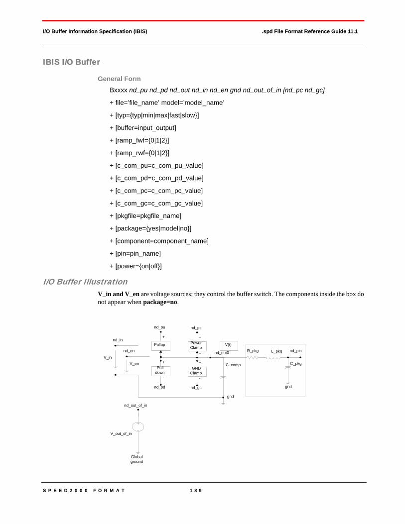
S P E E D 2 0 0 0 F O R M A T 1 8 9
I/O Buffer Information Specification (IBIS) .spd File Format Reference Guide 11.1
IBIS I/O Buffer
General Form Bxxxx nd_pu nd_pd nd_out nd_in nd_en gnd nd_out_of_in [nd_pc nd_gc]
+ file=’file_name’ model=’model_name’
+ [typ={typ|min|max|fast|slow}]
+ [buffer=input_output]
+ [ramp_fwf={0|1|2}]
+ [ramp_rwf={0|1|2}]
+ [c_com_pu=c_com_pu_value]
+ [c_com_pd=c_com_pd_value]
+ [c_com_pc=c_com_pc_value]
+ [c_com_gc=c_com_gc_value]
+ [pkgfile=pkgfile_name]
+ [package={yes|model|no}]
+ [component=component_name]
+ [pin=pin_name]
+ [power={on|off}]
I/O Buffer IllustrationV_in and V_en are voltage sources; they control the buffer switch. The components inside the box do not appear when package=no.
nd_gc
nd_pc
gnd
C_comp
PowerClamp
GNDClamp
+
-
+
-
Input/Ouptput Buffer
nd_pd
nd_pu
Pullup
Pulldown
+
-
+
-
gnd
C_pkg
L_pkgR_pkgV(t)
nd_pinnd_out0
nd_in
V_innd_en
V_en
Globalground
nd_out_of_in
V_out_of_in

S P E E D 2 0 0 0 F O R M A T 1 9 0
I/O Buffer Information Specification (IBIS) .spd File Format Reference Guide 11.1
IBIS I/O Buffer Parameter Descriptions
PARAMETER EFFECT OR MEANING
nd_pu Node of Pullup transistor
nd_pd Node of Pulldown transistor
nd_out
Because this is an I/O type buffer, nd_out can be used in two ways.
If the buffer is used as an input buffer, then nd_out is an input node. If the buffer is used as an output buffer, then nd_out is an output node. nd_out here is nd_out0.
nd_pin Appears only when package=yes and it functions as nd_out
nd_in Node which is linked with the triggering signal
nd_en Node which is linked with the ENABLE signal
gnd Ground node
nd_out_of_in Node which is linked with the digital signal of I/O buffer
nd_pc Node of power clamp
nd_gc Node of ground clamp
V_out_of_in
If I/O buffer is used as an input bufferIf I/O buffer is used as an output buffer or a tristate buffer
The buffer state is determined in the same way as in General Form.
The Tristate buffer has two major states: ENABLE and DISABLE. The ENABLE state differentiates between HIGH and LOW. There are totally three states for tristate buffer: LOW, HIGH and DISABLE.
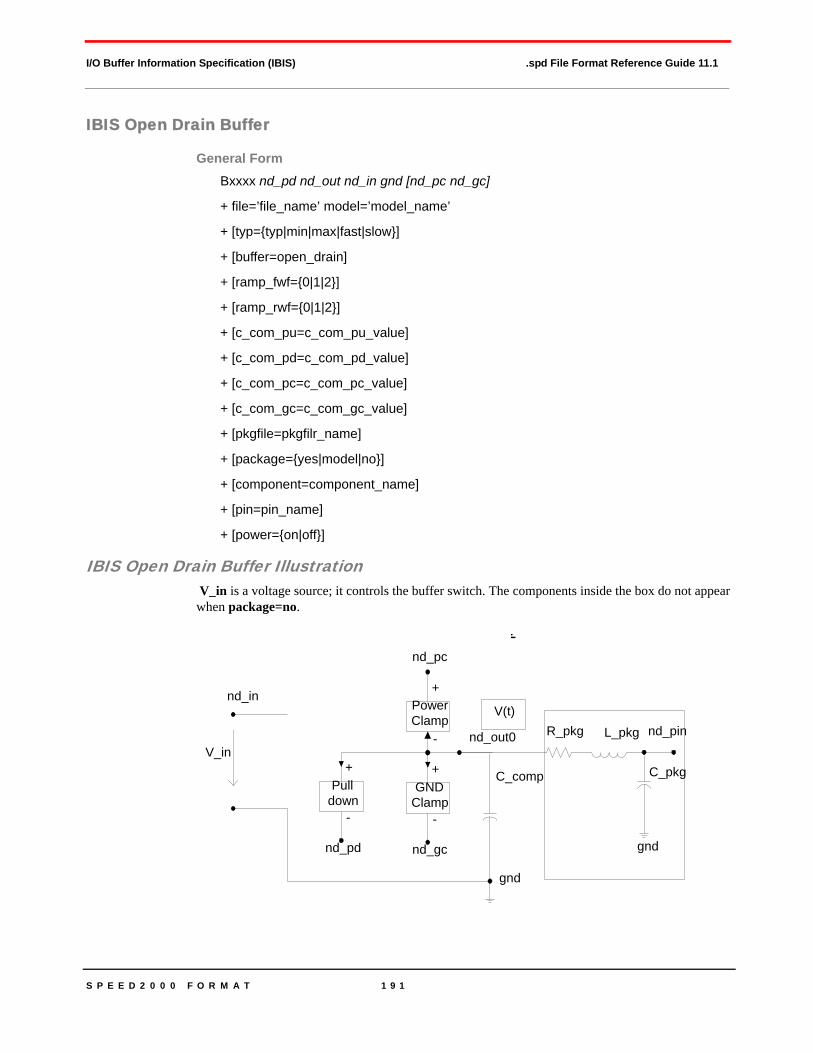
S P E E D 2 0 0 0 F O R M A T 1 9 1
I/O Buffer Information Specification (IBIS) .spd File Format Reference Guide 11.1
IBIS Open Drain Buffer
General FormBxxxx nd_pd nd_out nd_in gnd [nd_pc nd_gc]
+ file=’file_name’ model=’model_name’
+ [typ={typ|min|max|fast|slow}]
+ [buffer=open_drain]
+ [ramp_fwf={0|1|2}]
+ [ramp_rwf={0|1|2}]
+ [c_com_pu=c_com_pu_value]
+ [c_com_pd=c_com_pd_value]
+ [c_com_pc=c_com_pc_value]
+ [c_com_gc=c_com_gc_value]
+ [pkgfile=pkgfilr_name]
+ [package={yes|model|no}]
+ [component=component_name]
+ [pin=pin_name]
+ [power={on|off}]
IBIS Open Drain Buffer Illustration V_in is a voltage source; it controls the buffer switch. The components inside the box do not appear when package=no.
nd_gc
nd_pc
gnd
C_comp
PowerClamp
GNDClamp
+
-
+
-
Open Drain Buffer
nd_pd
Pulldown
-
+
nd_in
gnd
C_pkg
L_pkgR_pkgV(t)
nd_pinnd_out0V_in

S P E E D 2 0 0 0 F O R M A T 1 9 2
I/O Buffer Information Specification (IBIS) .spd File Format Reference Guide 11.1
IBIS Open Drain Buffer Parameter Descriptions
IBIS I/O Open Drain Buffer
General FormBxxxx nd_pd nd_out nd_in nd_en gnd nd_out_of_in [nd_pc nd_gc]
+ file=’file_name’ model=’model_name’
+ [typ={typ|min|max|fast|slow}]
+ [buffer=io_open_drain]
+ [ramp_fwf={0|1|2}]
+ [ramp_rwf={0|1|2}]
+ [c_com_pu=c_com_pu_value]
+ [c_com_pd=c_com_pd_value]
+ [c_com_pc=c_com_pc_value]
+ [c_com_gc=c_com_gc_value]
+ [pkgfile=pkgfile_name]
+ [package={yes|model|no}]
+ [component=component_name]
+ [pin=pin_name]
+ [power={on|off}]
PARAMETER EFFECT OR MEANING
nd_pd Node of Pulldown transistor
nd_out Node of output; also nd_out here is nd_out0 above
nd_pin Appears only when package=yes and it functions as nd_out.
nd_in Node which is linked with the triggering signal
gnd Ground node
nd_pc Node of power clamp
nd_gc Node of ground clamp
V_in Rules for determining buffer state same as Output Buffer
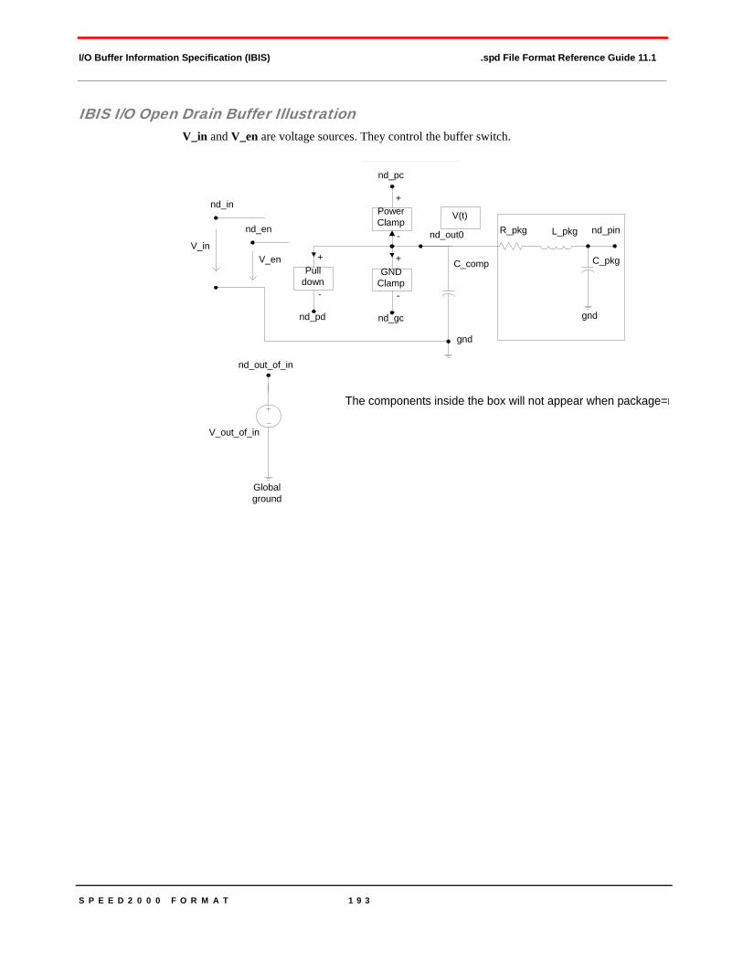
S P E E D 2 0 0 0 F O R M A T 1 9 3
I/O Buffer Information Specification (IBIS) .spd File Format Reference Guide 11.1
IBIS I/O Open Drain Buffer Illustration V_in and V_en are voltage sources. They control the buffer switch.
nd_gc
nd_pc
gnd
C_comp
PowerClamp
GNDClamp
+
-
+
-
nd_pd
Pulldown
-
+
nd_in
gnd
C_pkg
L_pkgR_pkgV(t)
nd_pinnd_out0V_in
Globalground
nd_out_of_in
V_out_of_in
nd_en
V_en
The components inside the box will not appear when package=n

S P E E D 2 0 0 0 F O R M A T 1 9 4
I/O Buffer Information Specification (IBIS) .spd File Format Reference Guide 11.1
IBIS I/O Open Drain Buffer Parameter Descriptions
PARAMETER EFFECT OR MEANING
nd_pd Node of Pulldown transistor
nd_out
I/O type buffer. nd_out can be used in two ways:
• If the buffer is used as an input buffer, then nd_out is an input node.
• If the buffer is used as an output buffer, then nd_out is an output node.
nd_out here is nd_out0.
nd_pin This node appears only when package=yes and it functions as nd_out
nd_in Node which is linked with the triggering signal
nd_en Node which is linked with the ENABLE signal
gnd Ground node
nd_out_of_in Node which is linked with the digital signal of I/O open drain buffer
nd_pc Node of power clamp
nd_gc Node of ground clamp
V_in Rules for determining buffer state same as I/O Buffer
V_en Rules for determining buffer state same as I/O Buffer
V_out_of_in Rules for determining buffer state same as I/O Buffer
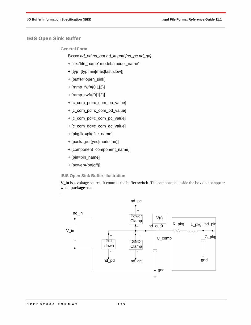
S P E E D 2 0 0 0 F O R M A T 1 9 5
I/O Buffer Information Specification (IBIS) .spd File Format Reference Guide 11.1
IBIS Open Sink Buffer
General FormBxxxx nd_pd nd_out nd_in gnd [nd_pc nd_gc]
+ file=’file_name’ model=’model_name’
+ [typ={typ|min|max|fast|slow}]
+ [buffer=open_sink]
+ [ramp_fwf={0|1|2}]
+ [ramp_rwf={0|1|2}]
+ [c_com_pu=c_com_pu_value]
+ [c_com_pd=c_com_pd_value]
+ [c_com_pc=c_com_pc_value]
+ [c_com_gc=c_com_gc_value]
+ [pkgfile=pkgfile_name]
+ [package={yes|model|no}]
+ [component=component_name]
+ [pin=pin_name]
+ [power={on|off}]
IBIS Open Sink Buffer IllustrationV_in is a voltage source. It controls the buffer switch. The components inside the box do not appear when package=no..
nd_gc
nd_pc
gnd
C_comp
PowerClamp
GNDClamp
+
-
+
-
nd_pd
Pulldown
-
+
nd_in
gnd
C_pkg
L_pkgR_pkgV(t)
nd_pinnd_out0V_in

S P E E D 2 0 0 0 F O R M A T 1 9 6
I/O Buffer Information Specification (IBIS) .spd File Format Reference Guide 11.1
IBIS Open Sink Buffer Parameter Descriptions
IBIS I/O Open Sink Buffer
General FormBxxxx nd_pd nd_out nd_in nd_en gnd nd_out_of_in [nd_pc nd_gc]
+ file=’file_name’ model=’model_name’
+ [typ={typ|min|max|fast|slow}]
+ [buffer=io_open_sink]
+ [ramp_fwf={0|1|2}]
+ [ramp_rwf={0|1|2}]
+ [c_com_pu=c_com_pu_value]
+ [c_com_pd=c_com_pd_value]
+ [c_com_pc=c_com_pc_value]
+ [c_com_gc=c_com_gc_value]
+ [pkgfile=pkgfile_name]
+ [package={yes|model|no}]
+ [component=component_name]
+ [pin=pin_name]
+ [power={on|off}]
PARAMETER EFFECT OR MEANING
nd_pd Node of Pulldown transistor
nd_out Node of output; also nd_out here is nd_out0 above
nd_pin Appears only when package=yes and it functions as nd_out.
nd_in Node which is linked with the triggering signal
gnd Ground node
nd_pc Node of power clamp
nd_gc Node of ground clamp
V_in Rules for determining buffer state are the same as Output Buffer
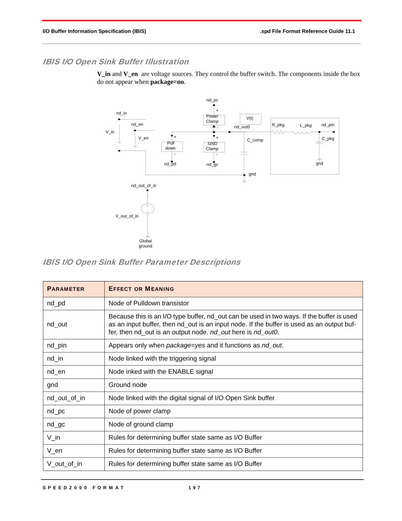
S P E E D 2 0 0 0 F O R M A T 1 9 7
I/O Buffer Information Specification (IBIS) .spd File Format Reference Guide 11.1
IBIS I/O Open Sink Buffer IllustrationV_in and V_en are voltage sources. They control the buffer switch. The components inside the box do not appear when package=no.
IBIS I/O Open Sink Buffer Parameter Descriptions
nd_gc
nd_pc
gnd
C_comp
PowerClamp
GNDClamp
+
-
+
-
nd_pd
Pulldown
-
+
nd_in
gnd
C_pkg
L_pkgR_pkgV(t)
nd_pinnd_out0V_in
Globalground
nd_out_of_in
V_out_of_in
nd_en
V_en
PARAMETER EFFECT OR MEANING
nd_pd Node of Pulldown transistor
nd_outBecause this is an I/O type buffer, nd_out can be used in two ways. If the buffer is used as an input buffer, then nd_out is an input node. If the buffer is used as an output buf-fer, then nd_out is an output node. nd_out here is nd_out0.
nd_pin Appears only when package=yes and it functions as nd_out.
nd_in Node linked with the triggering signal
nd_en Node inked with the ENABLE signal
gnd Ground node
nd_out_of_in Node linked with the digital signal of I/O Open Sink buffer
nd_pc Node of power clamp
nd_gc Node of ground clamp
V_in Rules for determining buffer state same as I/O Buffer
V_en Rules for determining buffer state same as I/O Buffer
V_out_of_in Rules for determining buffer state same as I/O Buffer

S P E E D 2 0 0 0 F O R M A T 1 9 8
I/O Buffer Information Specification (IBIS) .spd File Format Reference Guide 11.1
IBIS Open Source Buffer
General FormBxxxx nd_pu nd_out nd_in gnd [nd_pc nd_gc]
+ file=’file_name’ model=’model_name’
+ [typ={typ|min|max|fast|slow}]
+ [buffer=open_source]
+ [ramp_fwf={0|1|2}]
+ [ramp_rwf={0|1|2}]
+ [c_com_pu=c_com_pu_value]
+ [c_com_pd=c_com_pd_value]
+ [c_com_pc=c_com_pc_value]
+ [c_com_gc=c_com_gc_value]
+ [pkgfile=pkgfile_name]
+ [package={yes|model|no}]
+ [component=component_name]
+ [pin=pin_name]
+ [power={on|off}]
IBIS Open Source Buffer IllustrationV_in is a voltage source. It controls the buffer switch.
The components inside the box do not appear when package=no.
nd_gc
nd_pc
gnd
C_comp
PowerClamp
GNDClamp
+
-
+
-
Open Source Buffer
nd_pu
Pullup
+
-
nd_in
gnd
C_pkg
L_pkgR_pkgV(t)
nd_pinnd_out0V_in

S P E E D 2 0 0 0 F O R M A T 1 9 9
I/O Buffer Information Specification (IBIS) .spd File Format Reference Guide 11.1
IBIS Open Source Buffer Parameter Descriptions
PARAMETER EFFECT OR MEANING
nd_pu Node of Pullup transistor
nd_out Node of output. nd_out here is nd_out0 above
nd_pin Appears only when package=yes and it functions as nd_out
nd_in Node linked with the triggering signal
gnd Ground node
nd_pc Node of power clamp
nd_gc Node of ground clamp.
V_in Rules for determining buffer state same as Output Buffer

S P E E D 2 0 0 0 F O R M A T 2 0 0
I/O Buffer Information Specification (IBIS) .spd File Format Reference Guide 11.1
IBIS I/O Open Source Buffer
General FormBxxxx nd_pu nd_out nd_in nd_en gnd nd_out_of_in [nd_pc nd_gc]
+ file=’file_name’ model=’model_name’
+ [typ={typ|min|max|fast|slow}]
+ [buffer=io_open_source]
+ [ramp_fwf={0|1|2}]
+ [ramp_rwf={0|1|2}]
+ [c_com_pu=c_com_pu_value]
+ [c_com_pd=c_com_pd_value]
+ [c_com_pc=c_com_pc_value]
+ [c_com_gc=c_com_gc_value]
+ [pkgfile=pkgfile_name]
+ [package={yes|model|no}]
+ [component=component_name]
+ [pin=pin_name]
IBIS I/O Open Source Buffer IllustrationV_in and V_en are voltage sources. They control the buffer switch.
nd_gc
nd_pc
gnd
C_comp
PowerClamp
GNDClamp
+
-
+
-
nd_pu
Pullup
+
-
nd_in
gnd
C_pkg
L_pkgR_pkgV(t)
nd_pinnd_out0V_in
Globalground
nd_out_of_in
V_out_of_in
nd_en
V_en
The components inside the box will not appear when package=no.

S P E E D 2 0 0 0 F O R M A T 2 0 1
I/O Buffer Information Specification (IBIS) .spd File Format Reference Guide 11.1
IBIS I/O Open Source Buffer Parameter Descriptions
PARAMETER EFFECT OR MEANING
nd_pu Node of Pullup transistor
nd_out
I/O type buffer. nd_out can be used in two ways:
• If the buffer is used as an input buffer, then nd_out is an input node.
• If the buffer is used as an output buffer, then nd_out is an output node.
nd_out here is nd_out0.
nd_pin Appears only when package=yes and it functions as nd_out
nd_in Node which is linked with the triggering signal
nd_en Node which is linked with the ENABLE signal
gnd Ground node
nd_out_of_in Node which is linked with the digital signal of I/O Open
Source buffer
nd_pc Node of power clamp
nd_gc Node of ground clamp
V_in Rules for determining buffer state same as I/O Buffer
V_en Rules for determining buffer state same as I/O Buffer
V_out_of_in Rules for determining buffer state same as I/O Buffer

S P E E D 2 0 0 0 F O R M A T 2 0 2
I/O Buffer Information Specification (IBIS) .spd File Format Reference Guide 11.1
IBIS Input ECL Buffer
General FormBxxxx nd_pc nd_gc nd_in gnd nd_out_of_in
+ file=’file_name’ model=’model_name’
+ [typ={typ|min|max|fast|slow}]
+ [buffer=input_ecl]
+ [c_com_pu=c_com_pu_value]
+ [c_com_pd=c_com_pd_value]
+ [c_com_pc=c_com_pc_value]
+ [c_com_gc=c_com_gc_value]
+ [pkgfile=pkgfile_name]
+ [package={yes|model|no}]
+ [component=component_name]
+ [pin=pin_name]
IBIS Input ECL Buffer IllustrationThe input ECL buffer is similar to the input buffer. The only difference is in default values for Vinl and Vinh.
V_out_of_in is a digital signal controlled by voltage between nd_in0 and gnd.
The components inside the boxes do not appear when package = no.
nd_gc
nd_pc
Globalground
nd_out_of_in
V_out_of_in
PowerClamp
GNDClamp
nd_in0
+
-
+
-
INPUT ECL Buffer
gnd
C_comp
gnd
C_pkg
L_pkgR_pkg nd_pin
V(t)

S P E E D 2 0 0 0 F O R M A T 2 0 3
I/O Buffer Information Specification (IBIS) .spd File Format Reference Guide 11.1
IBIS Input ECL Buffer Parameter Descriptions
IBIS Output ECL Buffer
General FormBxxxx nd_pu nd_out nd_in gnd [nd_pc nd_gc]
+ file=’file_name’ model=’model_name’
+ [typ={typ|min|max|fast|slow}]
+ [buffer=output_ecl]
+ [ramp_fwf={0|1|2}]
+ [ramp_rwf={0|1|2}]
+ [c_com_pu=c_com_pu_value]
+ [c_com_pd=c_com_pd_value]
+ [c_com_pc=c_com_pc_value]
+ [c_com_gc=c_com_gc_value]
+ [pkgfile=pkgfile_name]
+ [package={yes|model|no}]
+ [component=component_name]
+ [pin=pin_name]
PARAMETER EFFECT OR MEANING
nd_pc Node of power clamp
nd_gc Node of ground clamp
nd_in Node of input, nd_in is nd_in0
nd_pin Appears only when package=yes and it functions as nd_in
gnd Ground node
nd_out_of_in Node which is linked with the digital signal of input ECL buffer
V_out_of_in Value of V_out_of_in is determined the same way as IBIS buffer

S P E E D 2 0 0 0 F O R M A T 2 0 4
I/O Buffer Information Specification (IBIS) .spd File Format Reference Guide 11.1
IBIS Out ECL Buffer IllustrationThe output ECL buffer does not have a pulldown node.
V_in is a voltage source linked between nd_in and gnd. It controls the buffer switch.
IBIS Output ECL Buffer Parameter Descriptions
nd_gc
nd_pc
gnd
C_comp
PowerClamp
GNDClamp
+
-
+
-
OUTPUT ECL Buffer
nd_pu
Pullup
Pulldown
+
-
+
-
nd_in
gnd
C_pkg
L_pkgR_pkgV(t)
nd_pinnd_out0V_in
The components inside the box will not appear when package=no.
PARAMETER EFFECT OR MEANING
nd_pu Node of Pullup transistor.
nd_out Node of output; also nd_out here is nd_out0 above.
nd_pin Appears only when package=yes and it functions as nd_out.
nd_in Node which is linked with the triggering signal.
gnd Ground node.
nd_pc Node of power clamp.
nd_gc Node of ground clamp.
V_in The rules for determining buffer state is the same as I/O Buffer.
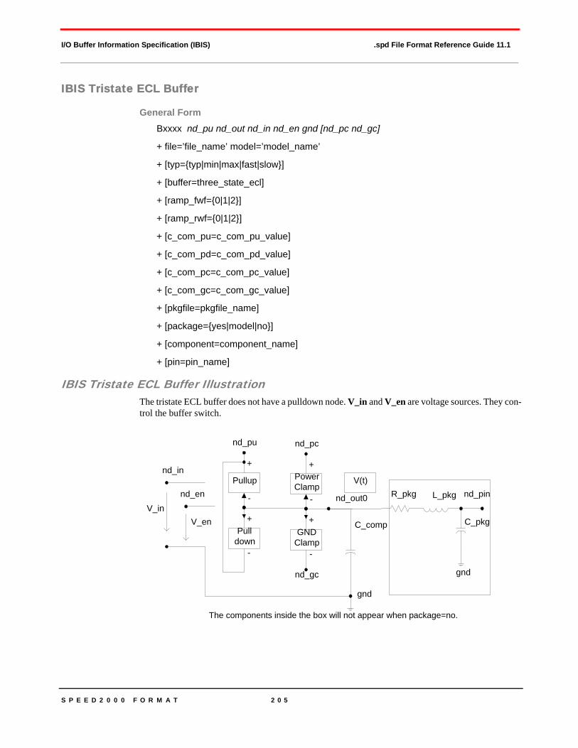
S P E E D 2 0 0 0 F O R M A T 2 0 5
I/O Buffer Information Specification (IBIS) .spd File Format Reference Guide 11.1
IBIS Tristate ECL Buffer
General FormBxxxx nd_pu nd_out nd_in nd_en gnd [nd_pc nd_gc]
+ file=’file_name’ model=’model_name’
+ [typ={typ|min|max|fast|slow}]
+ [buffer=three_state_ecl]
+ [ramp_fwf={0|1|2}]
+ [ramp_rwf={0|1|2}]
+ [c_com_pu=c_com_pu_value]
+ [c_com_pd=c_com_pd_value]
+ [c_com_pc=c_com_pc_value]
+ [c_com_gc=c_com_gc_value]
+ [pkgfile=pkgfile_name]
+ [package={yes|model|no}]
+ [component=component_name]
+ [pin=pin_name]
IBIS Tristate ECL Buffer IllustrationThe tristate ECL buffer does not have a pulldown node. V_in and V_en are voltage sources. They con-trol the buffer switch.
nd_gc
nd_pc
gnd
C_comp
PowerClamp
GNDClamp
+
-
+
-
nd_pu
Pullup
Pulldown
+
-
+
-
gnd
C_pkg
L_pkgR_pkgV(t)
nd_pinnd_out0
nd_in
V_innd_en
V_en
The components inside the box will not appear when package=no.

S P E E D 2 0 0 0 F O R M A T 2 0 6
I/O Buffer Information Specification (IBIS) .spd File Format Reference Guide 11.1
IBIS Tristate ECL Buffer Parameter Descriptions
PARAMETER EFFECT OR MEANING
nd_pu Node of Pullup transistor
nd_out Node of output; also nd_out here is nd_out0 above
nd_pin Appears only when package=yes and it functions as nd_out
nd_in Node linked with the triggering signal
nd_en Node linked with the ENABLE signal
gnd Ground node
nd_pc Node of power clamp
nd_gc Node of ground clamp
V_in Rules for determining buffer state same as I/O Buffer
V_en Rules for determining buffer state same as I/O Buffer

S P E E D 2 0 0 0 F O R M A T 2 0 7
I/O Buffer Information Specification (IBIS) .spd File Format Reference Guide 11.1
IBIS I/O ECL Buffer
General FormBxxxx nd_pu nd_out nd_in nd_en gnd nd_out_of_in [nd_pc nd_gc]
+ file=’file_name’ model=’model_name’
+ [typ={typ|min|max|fast|slow}]
+ [buffer=io_ecl]
+ [ramp_fwf={0|1|2}]
+ [ramp_rwf={0|1|2}]
+ [c_com_pu=c_com_pu_value]
+ [c_com_pd=c_com_pd_value]
+ [c_com_pc=c_com_pc_value]
+ [c_com_gc=c_com_gc_value]
+ [pkgfile=pkgfile_name]
+ [package={yes|model|no}]
+ [component=component_name]
+ [pin=pin_name]
IBIS I/O ECL Buffer IllustrationThe tristate ECL buffer does not have a pulldown node. V_in and V_en are voltage sources. They con-trol the buffer switch.
nd_gc
nd_pc
gnd
C_comp
PowerClamp
GNDClamp
+
-
+
-
I/O ECL Buffer
nd_pu
Pullup
Pulldown
+
-
+
-
gnd
C_pkg
L_pkgR_pkgV(t)
nd_pinnd_out0
nd_in
V_in
nd_en
V_en
Globalground
nd_out_of_in
V_out_of_in
The components inside the box will not appear when package=no.
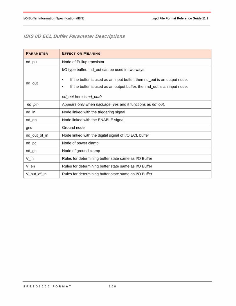
S P E E D 2 0 0 0 F O R M A T 2 0 8
I/O Buffer Information Specification (IBIS) .spd File Format Reference Guide 11.1
IBIS I/O ECL Buffer Parameter Descriptions
PARAMETER EFFECT OR MEANING
nd_pu Node of Pullup transistor
nd_out
I/O type buffer. nd_out can be used in two ways.
• If the buffer is used as an input buffer, then nd_out is an output node.
• If the buffer is used as an output buffer, then nd_out is an input node.
nd_out here is nd_out0.
nd_pin Appears only when package=yes and it functions as nd_out.
nd_in Node linked with the triggering signal
nd_en Node linked with the ENABLE signal
gnd Ground node
nd_out_of_in Node linked with the digital signal of I/O ECL buffer
nd_pc Node of power clamp
nd_gc Node of ground clamp
V_in Rules for determining buffer state same as I/O Buffer
V_en Rules for determining buffer state same as I/O Buffer
V_out_of_in Rules for determining buffer state same as I/O Buffer
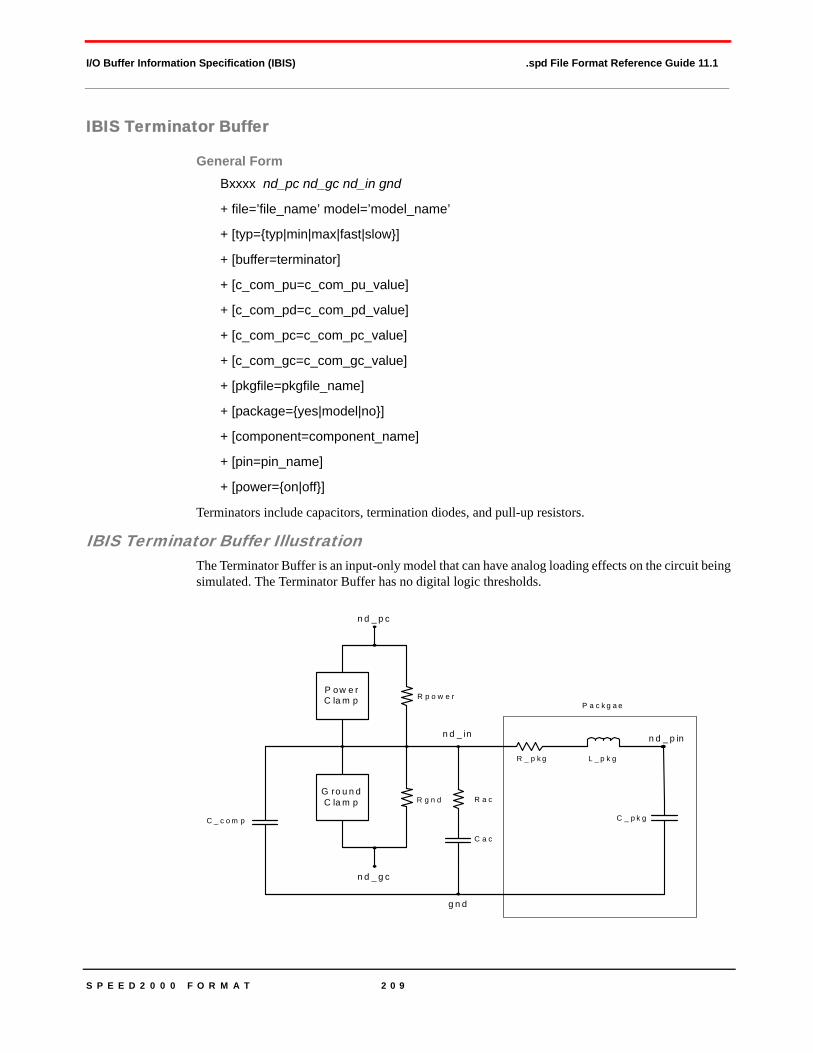
S P E E D 2 0 0 0 F O R M A T 2 0 9
I/O Buffer Information Specification (IBIS) .spd File Format Reference Guide 11.1
IBIS Terminator Buffer
General FormBxxxx nd_pc nd_gc nd_in gnd
+ file=’file_name’ model=’model_name’
+ [typ={typ|min|max|fast|slow}]
+ [buffer=terminator]
+ [c_com_pu=c_com_pu_value]
+ [c_com_pd=c_com_pd_value]
+ [c_com_pc=c_com_pc_value]
+ [c_com_gc=c_com_gc_value]
+ [pkgfile=pkgfile_name]
+ [package={yes|model|no}]
+ [component=component_name]
+ [pin=pin_name]
+ [power={on|off}]
Terminators include capacitors, termination diodes, and pull-up resistors.
IBIS Terminator Buffer IllustrationThe Terminator Buffer is an input-only model that can have analog loading effects on the circuit being simulated. The Terminator Buffer has no digital logic thresholds.
P ow e rC la m p
G ro u n dC la m p
n d _ p c
n d _ g c
g n d
n d _ in n d _ p in
C _ c o m p
R p o w e r
R g n d
C a c
R a c
R _ p k g L _ p k g
C _ p k g
P a c k g a e
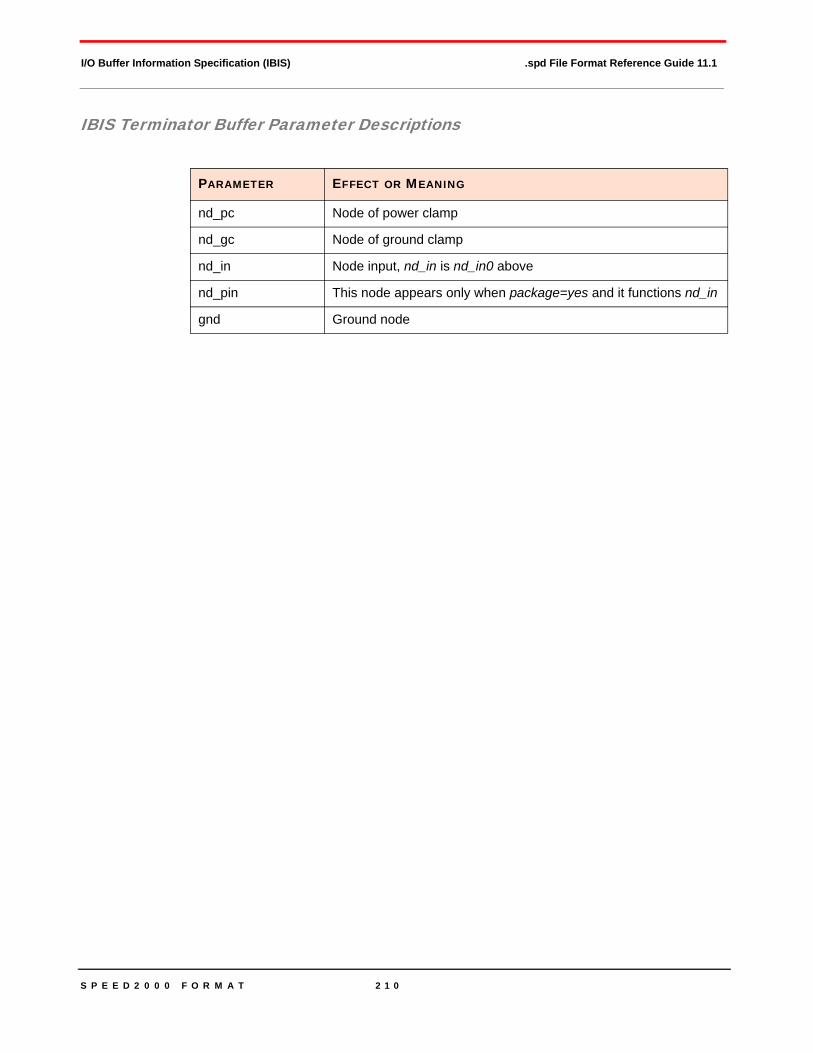
S P E E D 2 0 0 0 F O R M A T 2 1 0
I/O Buffer Information Specification (IBIS) .spd File Format Reference Guide 11.1
IBIS Terminator Buffer Parameter Descriptions
PARAMETER EFFECT OR MEANING
nd_pc Node of power clamp
nd_gc Node of ground clamp
nd_in Node input, nd_in is nd_in0 above
nd_pin This node appears only when package=yes and it functions nd_in
gnd Ground node
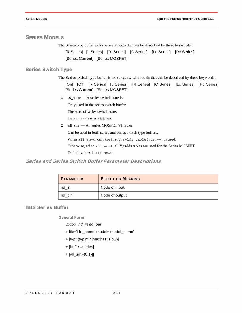
S P E E D 2 0 0 0 F O R M A T 2 1 1
Series Models .spd File Format Reference Guide 11.1
SERIES MODELSThe Series type buffer is for series models that can be described by these keywords:
[R Series] [L Series] [RI Series] [C Series] [Lc Series] [Rc Series]
[Series Current] [Series MOSFET]
Series Switch TypeThe Series_switch type buffer is for series switch models that can be described by these keywords:
[On] [Off] [R Series] [L Series] [RI Series] [C Series] [Lc Series] [Rc Series][Series Current] [Series MOSFET]
ss_state — A series switch state is:
Only used in the series switch buffer.
The state of series switch state.
Default value is ss_state=on.
all_sm — All series MOSFET VI tables.
Can be used in both series and series switch type buffers.
When all_sm=0, only the first Vgs-lds table(vds!=0) is used.
Otherwise, when all_sm=1, all Vgs-lds tables are used for the Series MOSFET.
Default values is all_sm=0.
Series and Series Switch Buffer Parameter Descriptions
IBIS Series Buffer
General FormBxxxx nd_in nd_out
+ file=’file_name’ model=’model_name’
+ [typ={typ|min|max|fast|slow}]
+ [buffer=series]
+ [all_sm={0|1}]]
PARAMETER EFFECT OR MEANING
nd_in Node of input.
nd_pin Node of output.

S P E E D 2 0 0 0 F O R M A T 2 1 2
Series Models .spd File Format Reference Guide 11.1
IBIS Series Buffer Parameter Descriptions
IBIS Series Switch Buffer
General FormBxxxx nd_in nd_out
+ file=’file_name’ model=’model_name’
+ [typ={typ|min|max|fast|slow}]
+ [buffer=series switch]
+ [ss_state={on|off}]
+ [all_sm={0|1}]
IBIS Series Switch Buffer Illustration
PARAMETER EFFECT OR MEANING
nd_in Node of input.
nd_pin Node of output.
R_series
L_series Rl_series
C_series Rc_series Lc_series
Series Current (V-I Table)
Series MOSFET (Vds-Ids Table)
nd_in nd_out
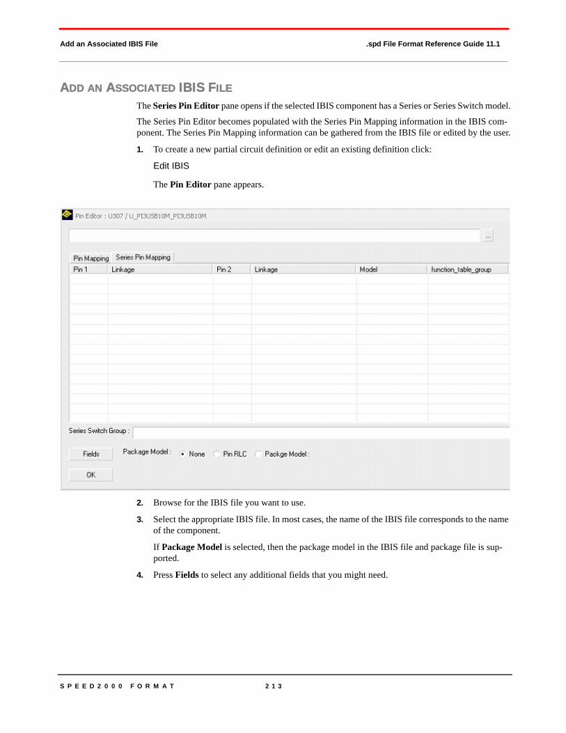
S P E E D 2 0 0 0 F O R M A T 2 1 3
Add an Associated IBIS File .spd File Format Reference Guide 11.1
ADD AN ASSOCIATED IBIS FILEThe Series Pin Editor pane opens if the selected IBIS component has a Series or Series Switch model.
The Series Pin Editor becomes populated with the Series Pin Mapping information in the IBIS com-ponent. The Series Pin Mapping information can be gathered from the IBIS file or edited by the user.
1. To create a new partial circuit definition or edit an existing definition click:
Edit IBIS
The Pin Editor pane appears.
2. Browse for the IBIS file you want to use.
3. Select the appropriate IBIS file. In most cases, the name of the IBIS file corresponds to the name of the component.
If Package Model is selected, then the package model in the IBIS file and package file is sup-ported.
4. Press Fields to select any additional fields that you might need.
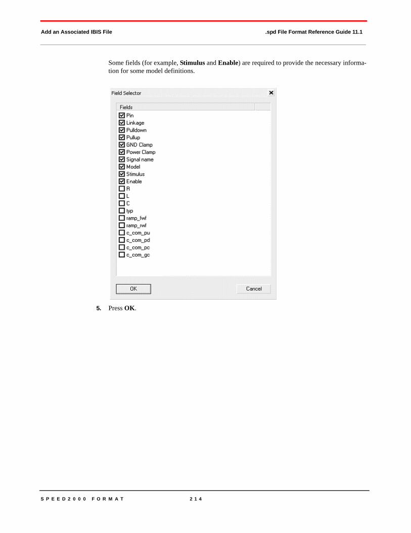
S P E E D 2 0 0 0 F O R M A T 2 1 4
Add an Associated IBIS File .spd File Format Reference Guide 11.1
Some fields (for example, Stimulus and Enable) are required to provide the necessary informa-tion for some model definitions.
5. Press OK.
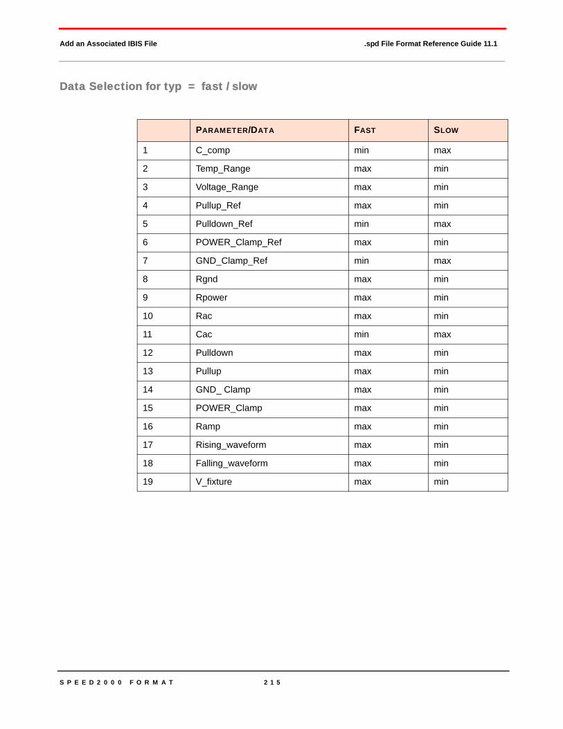
S P E E D 2 0 0 0 F O R M A T 2 1 5
Add an Associated IBIS File .spd File Format Reference Guide 11.1
Data Selection for typ = fast / slow
PARAMETER/DATA FAST SLOW
1 C_comp min max
2 Temp_Range max min
3 Voltage_Range max min
4 Pullup_Ref max min
5 Pulldown_Ref min max
6 POWER_Clamp_Ref max min
7 GND_Clamp_Ref min max
8 Rgnd max min
9 Rpower max min
10 Rac max min
11 Cac min max
12 Pulldown max min
13 Pullup max min
14 GND_ Clamp max min
15 POWER_Clamp max min
16 Ramp max min
17 Rising_waveform max min
18 Falling_waveform max min
19 V_fixture max min
S P E E D 2 0 0 0 F O R M A T 2 1 6
Circuit Solvers .spd File Format Reference Guide 11.1
CIRCUIT SOLVERSTwo types of circuit solvers are available in SPEED2000: External and HSPICE.
SPEED2000 can pass certain partial circuits to user specified external circuit solvers.
External Circuit Solver
General Form.ExternalCircuitSolver CircuitSolverName
External Circuit Solver Parameter Descriptions
.HSPICE Circuit SolversA data section enclosed by .HSPICE and .EndHSPICE keywords describes options used in HSPICE circuit solvers.
The position for the data section is right after .ExternalCircuitSolver statement.
General Form.HSPICE
.option post list node
HSPICE Example.HSPICE
.option post list node
.EndHSPICE
.EndHSPICE
General Form.EndHSPICE
PARAMETER EFFECT OR MEANING
.ExternalCircuitSolver Keyword for External Circuit Solver type.
CircuitSolverName One external circuit solver is supported. Values can only be HSPICE.
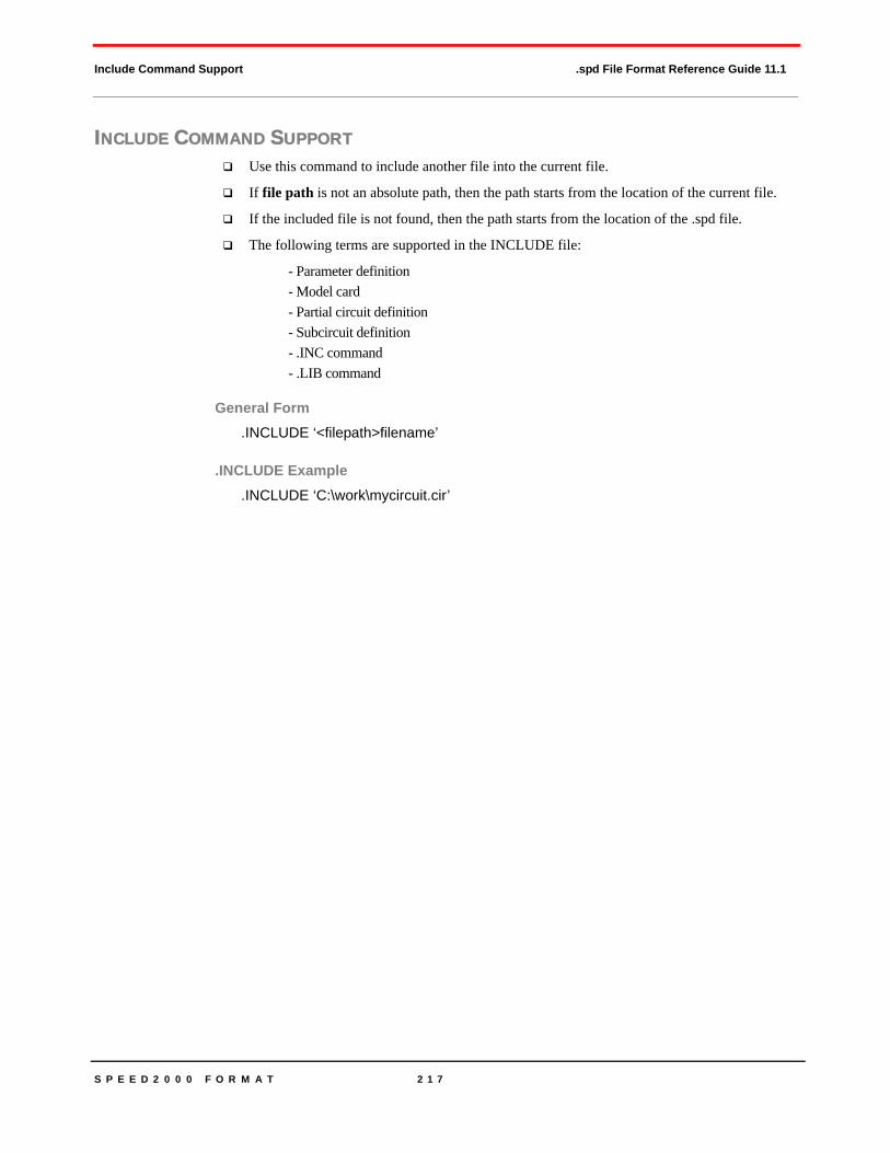
S P E E D 2 0 0 0 F O R M A T 2 1 7
Include Command Support .spd File Format Reference Guide 11.1
INCLUDE COMMAND SUPPORTUse this command to include another file into the current file.
If file path is not an absolute path, then the path starts from the location of the current file.
If the included file is not found, then the path starts from the location of the .spd file.
The following terms are supported in the INCLUDE file:
- Parameter definition- Model card- Partial circuit definition- Subcircuit definition- .INC command- .LIB command
General Form.INCLUDE ‘<filepath>filename’
.INCLUDE Example.INCLUDE ‘C:\work\mycircuit.cir’
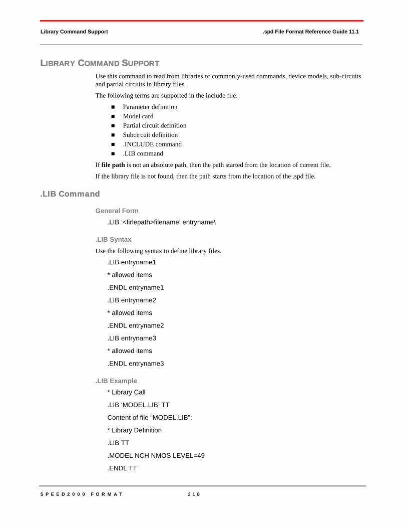
S P E E D 2 0 0 0 F O R M A T 2 1 8
Library Command Support .spd File Format Reference Guide 11.1
LIBRARY COMMAND SUPPORTUse this command to read from libraries of commonly-used commands, device models, sub-circuits and partial circuits in library files.
The following terms are supported in the include file:
Parameter definitionModel cardPartial circuit definitionSubcircuit definition.INCLUDE command.LIB command
If file path is not an absolute path, then the path started from the location of current file.
If the library file is not found, then the path starts from the location of the .spd file.
.LIB Command
General Form.LIB ‘<firlepath>filename’ entryname\
.LIB SyntaxUse the following syntax to define library files.
.LIB entryname1
* allowed items
.ENDL entryname1
.LIB entryname2
* allowed items
.ENDL entryname2
.LIB entryname3
* allowed items
.ENDL entryname3
.LIB Example* Library Call
.LIB ‘MODEL.LIB’ TT
Content of file “MODEL.LIB”:
* Library Definition
.LIB TT
.MODEL NCH NMOS LEVEL=49
.ENDL TT

219
Chapter
10MOSFET BSIM3v3 Model Parameters
This chapter contains a complete list of MOSFET BSIM3v3 (LEVEL 49/53) parameters.
MOSFET BSIM3V3 MODEL PARAMETER DESCRIPTIONS
PARAMETER (ALIAS) UNITS DEFAULT BINNING EFFECT OR MEANING
LEVEL - 1.0 NO Set LEVEL to 49 or 53 to identify the model as BSIM3v3 model.
VERSION - 3.30 NO Select from BSIM3 Version: 3.1, 3.2, 3.21, 3.22, 3.23, 3.24 and 3.30.
PARAMCHK - 0 NO Set PARAMCHK to 1 to check additional parameter value.
APWARN - 0 NO Set APWARN > 0 to turn off warning messages when PS/PD < Weff.
BINFLAG - 0 NO Set BINFLAG > 0.9 to use WREF, LREF in binning parameter calculation.
MOBMOD - 1 NO Mobility model selector.
CAPMOD - 3 NO Capacitance model selector.
ACM -
0 if LEVEL=4910 if LEVEL=53
NO
Selects MOS S/D parasitic model. Set ACM = 10, 11, 12, 13 to enable the Berkeley junction diode current and capacitance equation. The parasitic resistor equation corresponds to the ACM = 0, 1, 2, 3 equations.
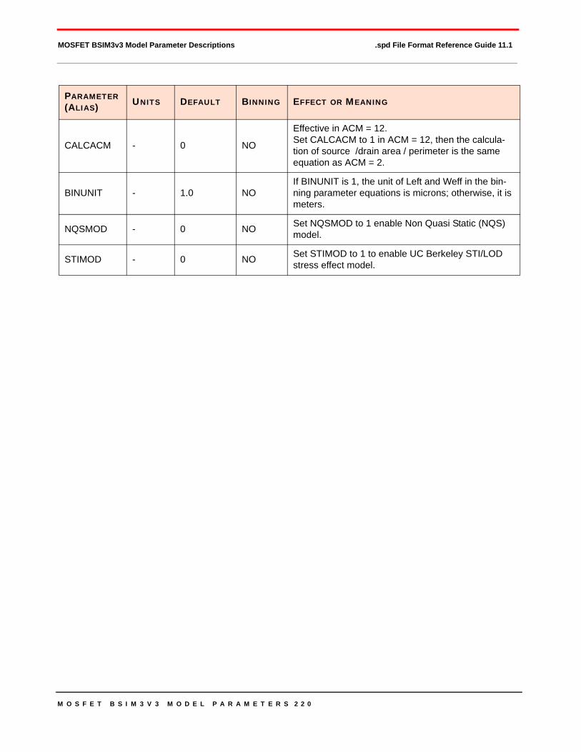
M O S F E T B S I M 3 V 3 M O D E L P A R A M E T E R S 2 2 0
MOSFET BSIM3v3 Model Parameter Descriptions .spd File Format Reference Guide 11.1
CALCACM - 0 NO
Effective in ACM = 12. Set CALCACM to 1 in ACM = 12, then the calcula-tion of source /drain area / perimeter is the same equation as ACM = 2.
BINUNIT - 1.0 NOIf BINUNIT is 1, the unit of Left and Weff in the bin-ning parameter equations is microns; otherwise, it is meters.
NQSMOD - 0 NO Set NQSMOD to 1 enable Non Quasi Static (NQS) model.
STIMOD - 0 NO Set STIMOD to 1 to enable UC Berkeley STI/LOD stress effect model.
PARAMETER (ALIAS) UNITS DEFAULT BINNING EFFECT OR MEANING

M O S F E T B S I M 3 V 3 M O D E L P A R A M E T E R S 2 2 1
MOSFET BSIM3v3 Model Parameter Descriptions .spd File Format Reference Guide 11.1
DC Parameters
PARAMETER (ALIAS) UNITS DEFAULT BINNING EFFECT OR MEANING
TOX m 1.5e-8 NO Gate oxide thickness.
TOXM m TOX NO Reference gate oxide thickness.
XJ m 1.5e-7 YES Junction depth.
GAMMA1 V1/2 Calculated YES Body-effect coefficient near the surface.
GAMMA2 V1/2 Calculated YES Body-effect coefficient in the bulk.
NCH 1/cm3 1.7e17 YES Channel doping concentration.
NSUB 1/cm3 6e16 YES Substrate doping concentration.
VBX V Calculated YES VBS at which the depletion region width equals to XT.
XT m 1.55e-7 YES Doping depth.
VTH0 (VTHO) V 0.7 (NMOS)
-0.7 (PMOS) YES Ideal threshold voltage of long channel device without body bias.
VFB V -3.0 YES Flat band voltage.
K1 V1/2 2.2 YES First order body effect coefficient.
K2 - 0.53 YES Second order body effect coefficient.
K3 - -0.032 YES Narrow width coefficient.
K3B 1/V 0.0 YES Body effect coefficient of narrow width coefficient.
W0 m 5.3e6 YES Narrow width parameter.
NLX m 1.74e-7 YES Lateral non-uniform doping parameter.
VBM V -3.0 YES Maximum applied body bias for Vth calculation.
DVT0 - 2.2 YES First coefficient of short-channel effect.
DVT1 - 0.53 YES Second coefficient of short-channel effect.
DVT2 1/V -0.032 YES Body-bias coefficient of short-channel effect.
DVT0W 1/m 0.0 YES First coefficient if narrow width effect in small channel length device.
DVT1W 1/m 5.3e6 YES Second coefficient of narrow width effect in small channel length device.
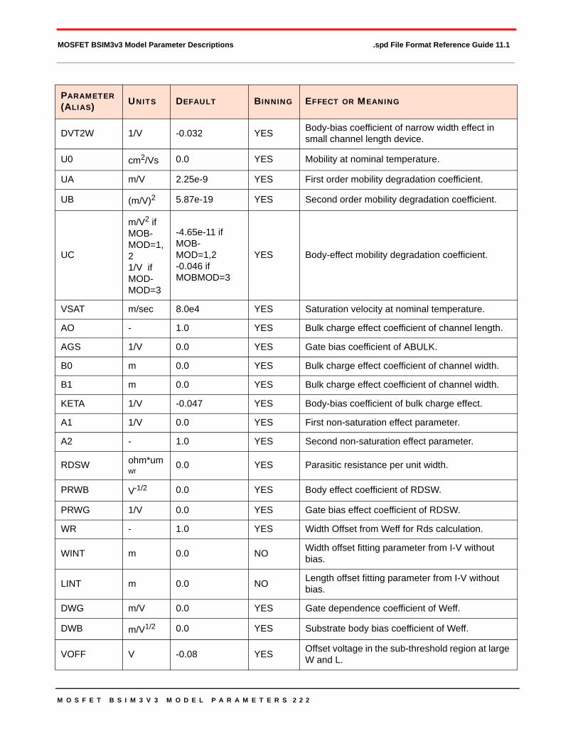
M O S F E T B S I M 3 V 3 M O D E L P A R A M E T E R S 2 2 2
MOSFET BSIM3v3 Model Parameter Descriptions .spd File Format Reference Guide 11.1
DVT2W 1/V -0.032 YES Body-bias coefficient of narrow width effect in small channel length device.
U0 cm2/Vs 0.0 YES Mobility at nominal temperature.
UA m/V 2.25e-9 YES First order mobility degradation coefficient.
UB (m/V)2 5.87e-19 YES Second order mobility degradation coefficient.
UC
m/V2 ifMOB-MOD=1,21/V ifMOD-MOD=3
-4.65e-11 ifMOB- MOD=1,2-0.046 ifMOBMOD=3
YES Body-effect mobility degradation coefficient.
VSAT m/sec 8.0e4 YES Saturation velocity at nominal temperature.
AO - 1.0 YES Bulk charge effect coefficient of channel length.
AGS 1/V 0.0 YES Gate bias coefficient of ABULK.
B0 m 0.0 YES Bulk charge effect coefficient of channel width.
B1 m 0.0 YES Bulk charge effect coefficient of channel width.
KETA 1/V -0.047 YES Body-bias coefficient of bulk charge effect.
A1 1/V 0.0 YES First non-saturation effect parameter.
A2 - 1.0 YES Second non-saturation effect parameter.
RDSW ohm*umwr
0.0 YES Parasitic resistance per unit width.
PRWB V-1/2 0.0 YES Body effect coefficient of RDSW.
PRWG 1/V 0.0 YES Gate bias effect coefficient of RDSW.
WR - 1.0 YES Width Offset from Weff for Rds calculation.
WINT m 0.0 NO Width offset fitting parameter from I-V without bias.
LINT m 0.0 NO Length offset fitting parameter from I-V without bias.
DWG m/V 0.0 YES Gate dependence coefficient of Weff.
DWB m/V1/2 0.0 YES Substrate body bias coefficient of Weff.
VOFF V -0.08 YES Offset voltage in the sub-threshold region at large W and L.
PARAMETER (ALIAS) UNITS DEFAULT BINNING EFFECT OR MEANING

M O S F E T B S I M 3 V 3 M O D E L P A R A M E T E R S 2 2 3
MOSFET BSIM3v3 Model Parameter Descriptions .spd File Format Reference Guide 11.1
NFACTOR - 1.0 YES Subthreshold swing factor.
ETA0 - 0.08 YES DIBL coefficient in subthreshold region.
ETAB 1/V -0.07 YES Body bias coefficient of the subthreshold DIBL effect.
DSUB - DROUT YES Subthreshold region DIBL coefficient exponent.
CIT F/m2 0.0 YES Interface trap capacitance.
CDSC F/m2 2.4e-4 YES Drain/Source to channel coupling capacitance.
CDSCB F/Vm2 0.0 YES Body-bias sensitivity of CDSC.
CDSCD F/Vm2 0.0 YES Drain-bias sensitivity of CDSC.
PCLM - 1.3 YES Channel length modulation parameter.
PDIBLC1 - 0.39 YES First output resistance DIBL effect correction parameter.
PDIBLC2 - 0.0086 YES Second output resistance DIBL effect correction parameter.
PDIBLCB 1/V 0 YES Body effect coefficient of DIBL correction parame-ters.
DROUT - 0.56 YES L dependence coefficient of the DIBL correction parameter in Rout.
PSCBE1 V/m 4.24e8 YES First substrate current body-effect parameter.
PSCBE2 m/V 1.0e-5 YES Second substrate current body-effect parameter.
PVAG - 0.0 YES Gate dependence of Early voltage.
DELTA V 0.01 YES Effective Vds parameter.
NGATE cm3 0 YES Polygate doping concentration.
ALPHA0 m/V 0 YES The first parameter of impact ionization current.
ALPHA1 1/V 0.0 YES Length scaling parameter of impact ionization current.
BETA0 V 30 YES The second parameter of impact ionization cur-rent.
RSH ohm/sq 0.0 NO Source/Drain sheet resistance.
JSW A/m 0.0 NO Source/Drain side wall saturation current density.
PARAMETER (ALIAS) UNITS DEFAULT BINNING EFFECT OR MEANING
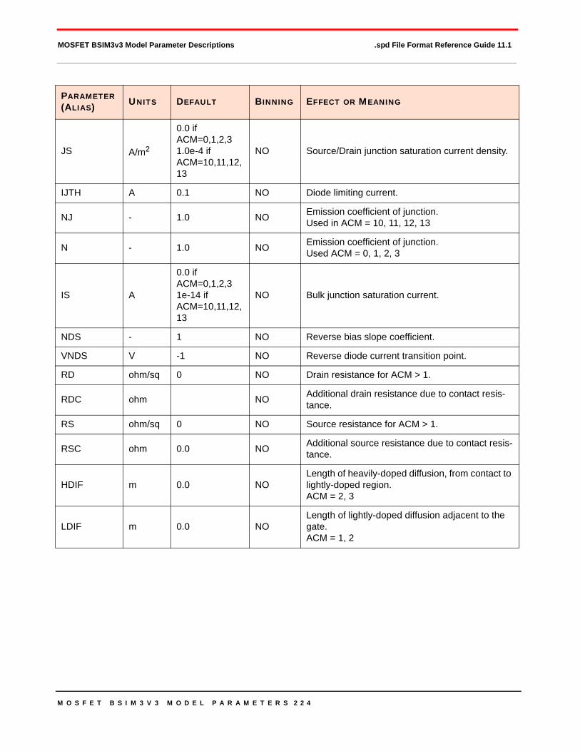
M O S F E T B S I M 3 V 3 M O D E L P A R A M E T E R S 2 2 4
MOSFET BSIM3v3 Model Parameter Descriptions .spd File Format Reference Guide 11.1
JS A/m2
0.0 ifACM=0,1,2,31.0e-4 ifACM=10,11,12,13
NO Source/Drain junction saturation current density.
IJTH A 0.1 NO Diode limiting current.
NJ - 1.0 NO Emission coefficient of junction.Used in ACM = 10, 11, 12, 13
N - 1.0 NO Emission coefficient of junction.Used ACM = 0, 1, 2, 3
IS A
0.0 ifACM=0,1,2,31e-14 ifACM=10,11,12,13
NO Bulk junction saturation current.
NDS - 1 NO Reverse bias slope coefficient.
VNDS V -1 NO Reverse diode current transition point.
RD ohm/sq 0 NO Drain resistance for ACM > 1.
RDC ohm NO Additional drain resistance due to contact resis-tance.
RS ohm/sq 0 NO Source resistance for ACM > 1.
RSC ohm 0.0 NO Additional source resistance due to contact resis-tance.
HDIF m 0.0 NOLength of heavily-doped diffusion, from contact to lightly-doped region. ACM = 2, 3
LDIF m 0.0 NOLength of lightly-doped diffusion adjacent to the gate. ACM = 1, 2
PARAMETER (ALIAS) UNITS DEFAULT BINNING EFFECT OR MEANING
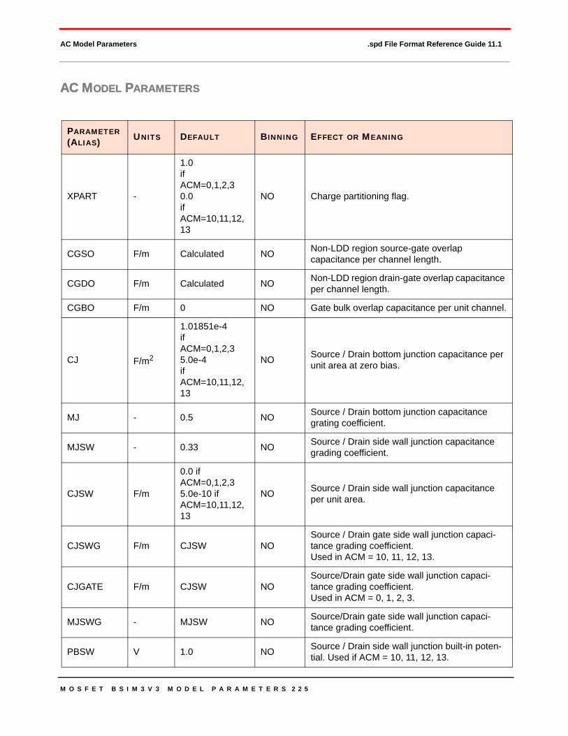
M O S F E T B S I M 3 V 3 M O D E L P A R A M E T E R S 2 2 5
AC Model Parameters .spd File Format Reference Guide 11.1
AC MODEL PARAMETERS
PARAMETER (ALIAS) UNITS DEFAULT BINNING EFFECT OR MEANING
XPART -
1.0 ifACM=0,1,2,30.0 ifACM=10,11,12,13
NO Charge partitioning flag.
CGSO F/m Calculated NO Non-LDD region source-gate overlap capacitance per channel length.
CGDO F/m Calculated NO Non-LDD region drain-gate overlap capacitance per channel length.
CGBO F/m 0 NO Gate bulk overlap capacitance per unit channel.
CJ F/m2
1.01851e-4 ifACM=0,1,2,35.0e-4 ifACM=10,11,12,13
NO Source / Drain bottom junction capacitance per unit area at zero bias.
MJ - 0.5 NO Source / Drain bottom junction capacitance grating coefficient.
MJSW - 0.33 NO Source / Drain side wall junction capacitance grading coefficient.
CJSW F/m
0.0 ifACM=0,1,2,35.0e-10 ifACM=10,11,12,13
NO Source / Drain side wall junction capacitance per unit area.
CJSWG F/m CJSW NOSource / Drain gate side wall junction capaci-tance grading coefficient. Used in ACM = 10, 11, 12, 13.
CJGATE F/m CJSW NOSource/Drain gate side wall junction capaci-tance grading coefficient.Used in ACM = 0, 1, 2, 3.
MJSWG - MJSW NO Source/Drain gate side wall junction capaci-tance grading coefficient.
PBSW V 1.0 NO Source / Drain side wall junction built-in poten-tial. Used if ACM = 10, 11, 12, 13.

M O S F E T B S I M 3 V 3 M O D E L P A R A M E T E R S 2 2 6
AC Model Parameters .spd File Format Reference Guide 11.1
PHB V PB NO Source / Drain side wall junction built-in poten-tial. Used if ACM = 0, 1, 2, 3.
PB V
0.8 ifACM=0,1,2,31.0 ifACM=10,11,12,13
NO Source / Drain bottom built-in potential.
PBSWG V PBSW NO Source / Drain gate side wall junction built-in potential.
CGSL F/m 0.0 YES Light doped source-gate region overlap capacitance.
CGDL F/m 0.0 YES Light doped drain-gate region overlap capacitance.
CKAPPA V 0.6 YES Coefficient for lightly doped region overlap capacitance fringing field capacitance.
CF F/m Calculated YES Fringing field capacitance.
CLC m 0.1e-6 YES Constant term for the short channel model.
CLE - 0.6 YES Exponential term for the short channel model.
DLC m LINT YES Length offset fitting parameter from C-V.
DWC m WINT YES Width offset fitting parameter from C-V.
VFBCV V -1 YES Flat-band voltage parameter for CAPMOD = 0 only.
ACDE m/V 1.0 YESExponential coefficient for charge thickness in CAPMOD = 3 for accumulation and depletion regions.
MOIN - 15.0 YES Coefficient for the gate-bias dependent surface potential.
CBD F 0 NO Zero bias bulk-drain junction capitulating. Used only if CJ and CJSW are 0.0.
CBS F 0 NO Zero bias bulk-source junction capacitance. Use only if CJ and CJSW are 0.0.
TT s 0 NO Transit time.
PARAMETER (ALIAS) UNITS DEFAULT BINNING EFFECT OR MEANING

M O S F E T B S I M 3 V 3 M O D E L P A R A M E T E R S 2 2 7
Geometry Parameters .spd File Format Reference Guide 11.1
GEOMETRY PARAMETERS
PARAMETER (ALIAS) UNITS DEFAULT BINNING EFFECT OR MEANING
LL mLLN 0.0 NO Coefficient of length dependence of length offset.
LLN - 1.0 NO Power of length dependence of length offset.
LW mLWN 0.0 NO Coefficient of width dependence of length offset.
LWL mLWN+L
LN0.0 NO Coefficient of length and width cross term of width
offset.
WL mWLN 0.0 NO Coefficient of length dependence of width offset.
WLN - 1.0 NO Power of length dependence of width offset.
WW mWWN 0.0 NO Coefficient of width dependence of width offset.
WWN - 1.0 NO Power of width dependence of width offset.
WWL mWWN+
WLN0.0 NO Coefficient of length and width cross term of width
offset.
LLC mLLN LL NO Coefficient of length dependence of channel length offset.
LWC mLWN LW NO Coefficient of width dependence of C-V channel length offset.
LWLC mLWN+L
LNLWL NO Coefficient of length and width dependence of C-V
channel length offset.
WLC mWLN WL NO Coefficient of length dependence of C-V channel width offset.
WWC mWWN WW NO Coefficient of width dependence of C-V channel width offset.
WWLC mWWN+
WLNWWL NO Coefficient of length and width dependence of C-V
channel width offset.
LMIN m 0.0 NO Minimum channel length.
LMAX m 1.0 NO Maximum channel length.
WMIN m 0.0 NO Minimum channel width.
WMAX m 1.0 NO Maximum channel width.
DEL m 0.0 NO Channel length reduction on each side.
LMT - 1.0 NO Gate length shrink factor.
LREF m 0.0 NO Channel length reference.

M O S F E T B S I M 3 V 3 M O D E L P A R A M E T E R S 2 2 8
Geometry Parameters .spd File Format Reference Guide 11.1
WMLT - 1.0 NO Diffusion layer and width shrink factor.
WREF m 0.0 NO Channel width reference.
XL(DL, LDEL) m 0.0 NO Length bias accounts for the masking and etching
effects.
XLREF m 0.0 NO Difference between the physical (on the wafer) and the drawn reference channel length.
XW m 0.0 NO Difference between the physical (on the wafer) and the drawn S/D active width.
XWREF m 0.0 NO Difference between the physical (on the wafer) and the drawn reference channel width.
PARAMETER (ALIAS) UNITS DEFAULT BINNING EFFECT OR MEANING

M O S F E T B S I M 3 V 3 M O D E L P A R A M E T E R S 2 2 9
Temperature Parameters .spd File Format Reference Guide 11.1
TEMPERATURE PARAMETERS
PARAMETER (ALIAS) UNITS DEFAULT BINNING EFFECT OR MEANING
UTE - -1.5 YES Mobility temperature exponent.
KT1 V -0.11 YES Temperature coefficient for threshold voltage.
KT1L Vm 0.0 YES Channel length dependence of the temperature coef-ficient for threshold voltage.
KT2 - 0.022 YES Body-bias coefficient of Vth temperature effect.
UA1 m/V 4.31e-9 YES Temperature coefficient for Ua.
UB1 (m/V)2 -7.61e-18 YES Temperature coefficient for Ub.
UC1
m/V2 ifMOB-MOD=1/21/V ifMOB-MOD=3
-5.6e-11 ifMOB-MOD=1/2-0.056 ifMOB-MOD=3
YES Temperature coefficient for Uc.
AT m/sec 3.3e4 YES Temperature coefficient for saturation velocity.
PRT ohm*um 0.0 YES Temperature coefficient for Rdsw.
XTI - 3.0 YES Junction current temperature exponent coefficient.
TPB V/K 0.0 NO Temperature coefficient of PB.
TPBSW V/K 0.0 NO Temperature coefficient of PBSW.
TPBSWG V/K 0.0 NO Temperature coefficient of PBSWG.
TCJ 1/K 0.0 NO Temperature coefficient of CJ.
TCJSW 1/K 0.0 NO Temperature coefficient of CJSW.
TCJSWG 1/k 0.0 NO Temperature coefficient of CJSWG.

M O S F E T B S I M 3 V 3 M O D E L P A R A M E T E R S 2 3 0
STI/LOD Model Parameters .spd File Format Reference Guide 11.1
STI/LOD MODEL PARAMETERS
PARAMETER (ALIAS) UNITS DEFAULT BINNING EFFECT OR MEANING
SAREF m 1.0e-6 No Reference distance between OD and edge to poly of one side.
SBREF m 1.0e-6 No Reference distance between OD and edge to poly of the other side.
WLOD m 0.0 No Width parameter for stress effect.
KU0 m 0.0 No Mobility degradation/enhancement coefficient for stress effect.
KVSAT m 0.0 No Saturation velocity degradation / enhancement parameter for stress effect.
TKU0 - 0.0 No Temperature coefficient of KU0.
LKU0 - 0.0 No Length dependence of KU0.
WKU0 - 0.0 No Width dependence of KU0.
PKU0 - 0.0 No Cross-term dependence of KU0.
LLODKU0 - 0.0 No Length parameter for u0 stress effect.
WLODKU0 - 0.0 No Width parameter for u0 stress effect.
KVTH0 V 0.0 No Threshold shift parameter for stress effect.
LKVTH0 - 0.0 No Length dependence of KVTH0.
WKVTH0 - 0.0 No Width dependence of KVTH0.
PKVTH0 - 0.0 No Cross-term dependence of KVTH0.
LLODVTH - 0.0 No Length parameter for Vth stress effect.
STK2 m 0.0 No K2 shift factor related to Vth0 change.
LODK2 - 1.0 No K2 shift modification factor for stress effect.
STETA0 m 0.0 No Eta0 shift factor related to Vth0.
LODETA0 - 1.0 No Eta0 shift modification factor for stress effect.
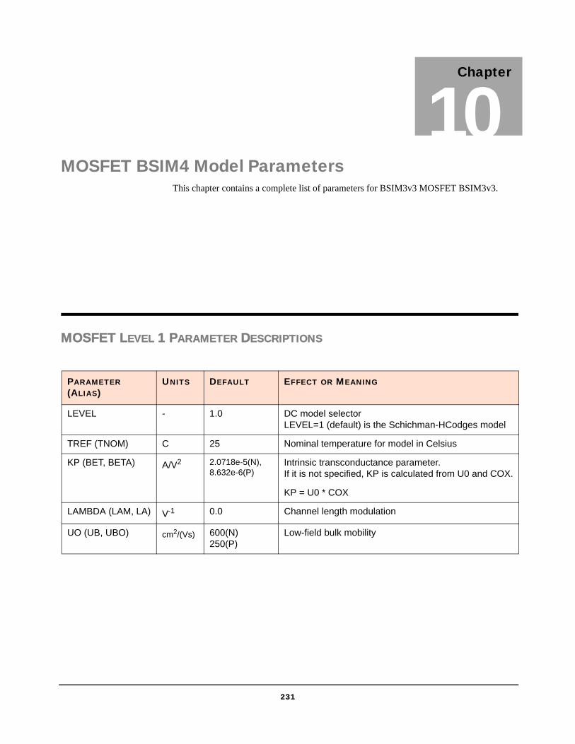
231
Chapter
10MOSFET BSIM4 Model Parameters
This chapter contains a complete list of parameters for BSIM3v3 MOSFET BSIM3v3.
MOSFET LEVEL 1 PARAMETER DESCRIPTIONS
PARAMETER (ALIAS)
UNITS DEFAULT EFFECT OR MEANING
LEVEL - 1.0 DC model selectorLEVEL=1 (default) is the Schichman-HCodges model
TREF (TNOM) C 25 Nominal temperature for model in Celsius
KP (BET, BETA) A/V2 2.0718e-5(N),8.632e-6(P)
Intrinsic transconductance parameter. If it is not specified, KP is calculated from U0 and COX.
KP = U0 * COX
LAMBDA (LAM, LA) V-1 0.0 Channel length modulation
UO (UB, UBO) cm2/(Vs) 600(N)250(P)
Low-field bulk mobility
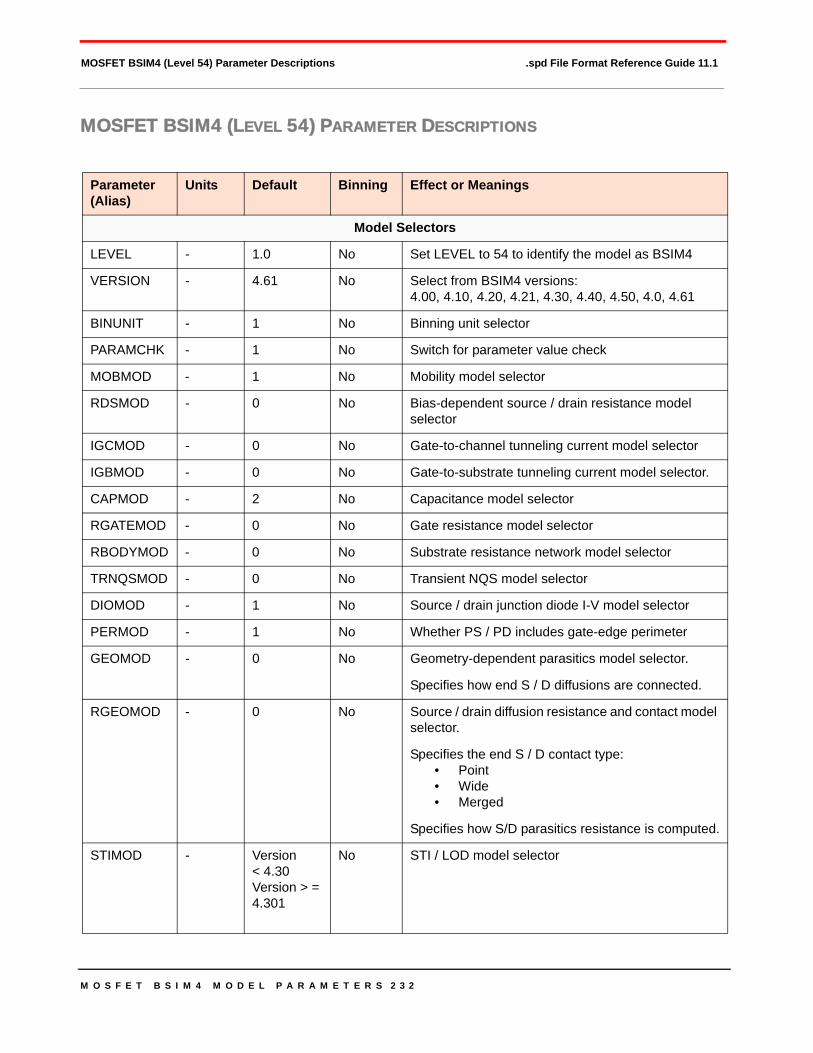
M O S F E T B S I M 4 M O D E L P A R A M E T E R S 2 3 2
MOSFET BSIM4 (Level 54) Parameter Descriptions .spd File Format Reference Guide 11.1
MOSFET BSIM4 (LEVEL 54) PARAMETER DESCRIPTIONS
Parameter (Alias)
Units Default Binning Effect or Meanings
Model Selectors
LEVEL - 1.0 No Set LEVEL to 54 to identify the model as BSIM4
VERSION - 4.61 No Select from BSIM4 versions:4.00, 4.10, 4.20, 4.21, 4.30, 4.40, 4.50, 4.0, 4.61
BINUNIT - 1 No Binning unit selector
PARAMCHK - 1 No Switch for parameter value check
MOBMOD - 1 No Mobility model selector
RDSMOD - 0 No Bias-dependent source / drain resistance model selector
IGCMOD - 0 No Gate-to-channel tunneling current model selector
IGBMOD - 0 No Gate-to-substrate tunneling current model selector.
CAPMOD - 2 No Capacitance model selector
RGATEMOD - 0 No Gate resistance model selector
RBODYMOD - 0 No Substrate resistance network model selector
TRNQSMOD - 0 No Transient NQS model selector
DIOMOD - 1 No Source / drain junction diode I-V model selector
PERMOD - 1 No Whether PS / PD includes gate-edge perimeter
GEOMOD - 0 No Geometry-dependent parasitics model selector.
Specifies how end S / D diffusions are connected.
RGEOMOD - 0 No Source / drain diffusion resistance and contact model selector.
Specifies the end S / D contact type: • Point• Wide• Merged
Specifies how S/D parasitics resistance is computed.
STIMOD - Version< 4.30Version > =4.301
No STI / LOD model selector
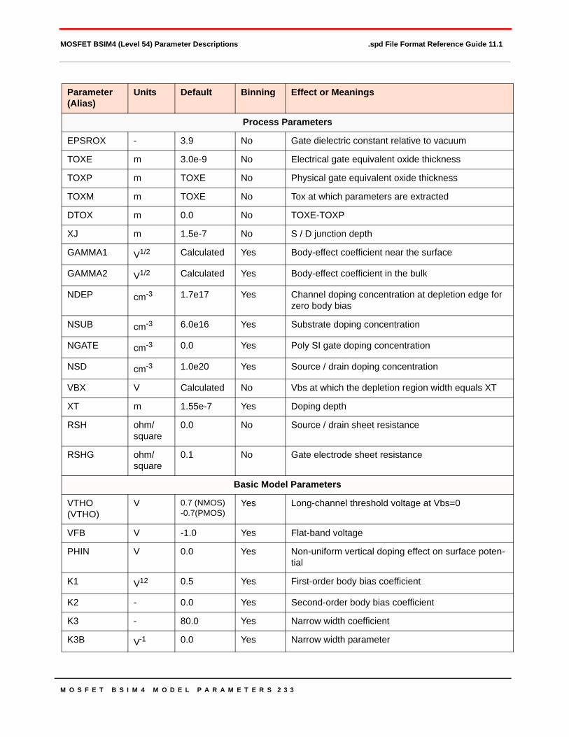
M O S F E T B S I M 4 M O D E L P A R A M E T E R S 2 3 3
MOSFET BSIM4 (Level 54) Parameter Descriptions .spd File Format Reference Guide 11.1
Process Parameters
EPSROX - 3.9 No Gate dielectric constant relative to vacuum
TOXE m 3.0e-9 No Electrical gate equivalent oxide thickness
TOXP m TOXE No Physical gate equivalent oxide thickness
TOXM m TOXE No Tox at which parameters are extracted
DTOX m 0.0 No TOXE-TOXP
XJ m 1.5e-7 No S / D junction depth
GAMMA1 V1/2 Calculated Yes Body-effect coefficient near the surface
GAMMA2 V1/2 Calculated Yes Body-effect coefficient in the bulk
NDEP cm-3 1.7e17 Yes Channel doping concentration at depletion edge for zero body bias
NSUB cm-3 6.0e16 Yes Substrate doping concentration
NGATE cm-3 0.0 Yes Poly SI gate doping concentration
NSD cm-3 1.0e20 Yes Source / drain doping concentration
VBX V Calculated No Vbs at which the depletion region width equals XT
XT m 1.55e-7 Yes Doping depth
RSH ohm/square
0.0 No Source / drain sheet resistance
RSHG ohm/square
0.1 No Gate electrode sheet resistance
Basic Model Parameters
VTHO (VTHO)
V 0.7 (NMOS) -0.7(PMOS)
Yes Long-channel threshold voltage at Vbs=0
VFB V -1.0 Yes Flat-band voltage
PHIN V 0.0 Yes Non-uniform vertical doping effect on surface poten-tial
K1 V12 0.5 Yes First-order body bias coefficient
K2 - 0.0 Yes Second-order body bias coefficient
K3 - 80.0 Yes Narrow width coefficient
K3B V-1 0.0 Yes Narrow width parameter
Parameter (Alias)
Units Default Binning Effect or Meanings
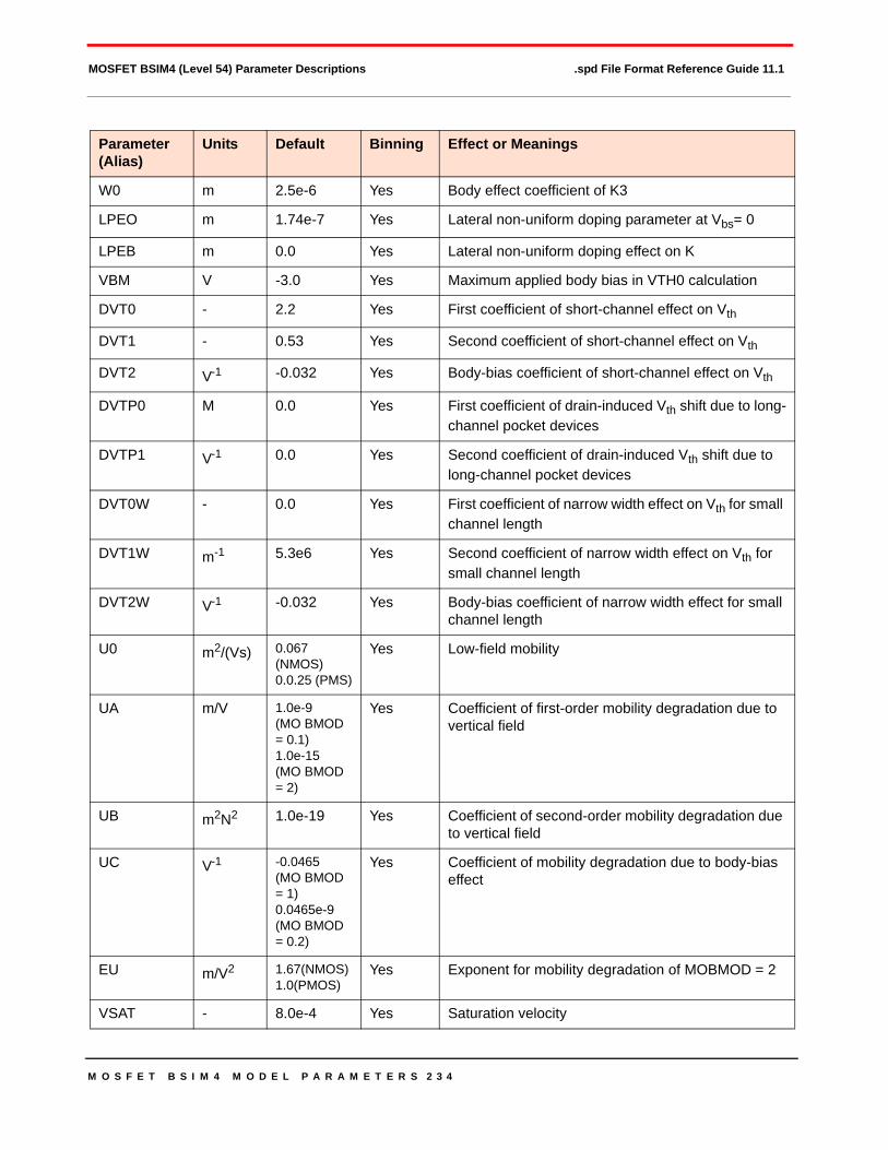
M O S F E T B S I M 4 M O D E L P A R A M E T E R S 2 3 4
MOSFET BSIM4 (Level 54) Parameter Descriptions .spd File Format Reference Guide 11.1
W0 m 2.5e-6 Yes Body effect coefficient of K3
LPEO m 1.74e-7 Yes Lateral non-uniform doping parameter at Vbs= 0
LPEB m 0.0 Yes Lateral non-uniform doping effect on K
VBM V -3.0 Yes Maximum applied body bias in VTH0 calculation
DVT0 - 2.2 Yes First coefficient of short-channel effect on Vth
DVT1 - 0.53 Yes Second coefficient of short-channel effect on Vth
DVT2 V-1 -0.032 Yes Body-bias coefficient of short-channel effect on Vth
DVTP0 M 0.0 Yes First coefficient of drain-induced Vth shift due to long-channel pocket devices
DVTP1 V-1 0.0 Yes Second coefficient of drain-induced Vth shift due to long-channel pocket devices
DVT0W - 0.0 Yes First coefficient of narrow width effect on Vth for small channel length
DVT1W m-1 5.3e6 Yes Second coefficient of narrow width effect on Vth for small channel length
DVT2W V-1 -0.032 Yes Body-bias coefficient of narrow width effect for small channel length
U0 m2/(Vs) 0.067 (NMOS)0.0.25 (PMS)
Yes Low-field mobility
UA m/V 1.0e-9 (MO BMOD = 0.1)1.0e-15 (MO BMOD = 2)
Yes Coefficient of first-order mobility degradation due to vertical field
UB m2N2 1.0e-19 Yes Coefficient of second-order mobility degradation due to vertical field
UC V-1 -0.0465 (MO BMOD = 1)0.0465e-9 (MO BMOD = 0.2)
Yes Coefficient of mobility degradation due to body-bias effect
EU m/V2 1.67(NMOS)1.0(PMOS)
Yes Exponent for mobility degradation of MOBMOD = 2
VSAT - 8.0e-4 Yes Saturation velocity
Parameter (Alias)
Units Default Binning Effect or Meanings
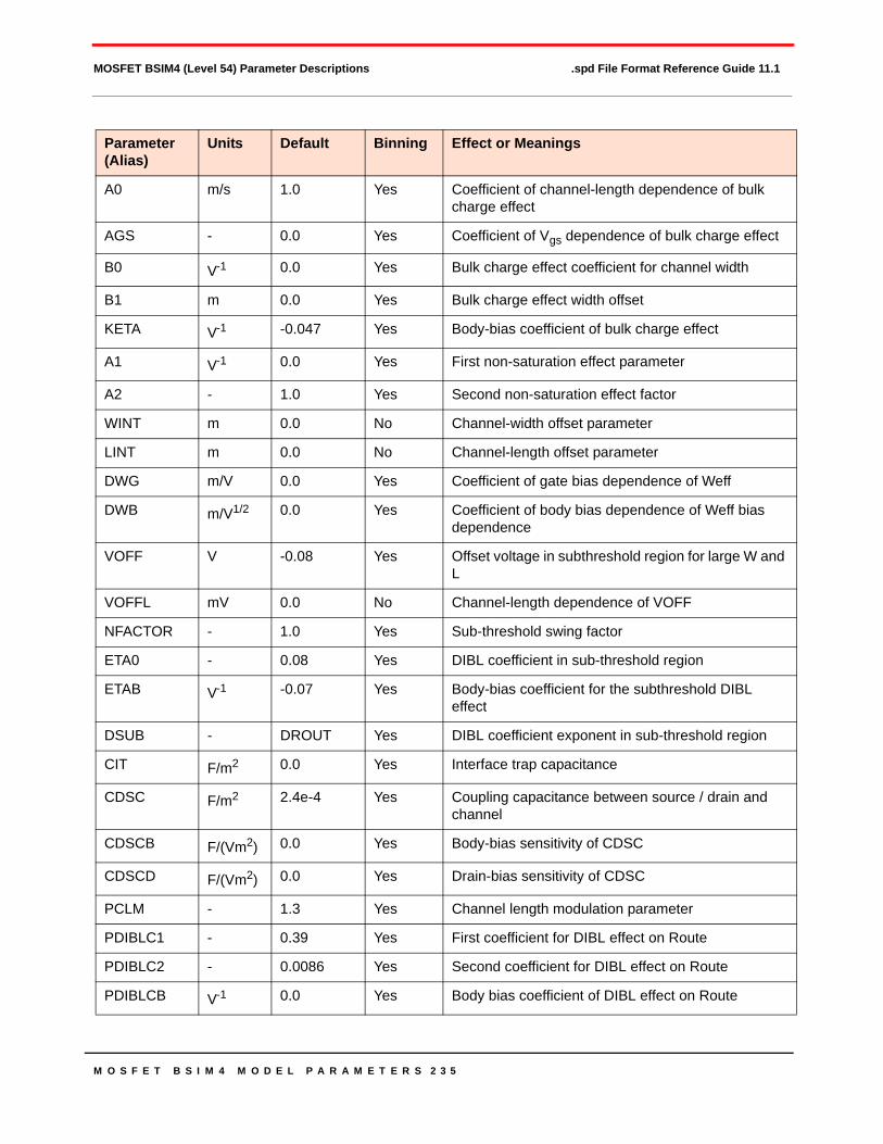
M O S F E T B S I M 4 M O D E L P A R A M E T E R S 2 3 5
MOSFET BSIM4 (Level 54) Parameter Descriptions .spd File Format Reference Guide 11.1
A0 m/s 1.0 Yes Coefficient of channel-length dependence of bulk charge effect
AGS - 0.0 Yes Coefficient of Vgs dependence of bulk charge effect
B0 V-1 0.0 Yes Bulk charge effect coefficient for channel width
B1 m 0.0 Yes Bulk charge effect width offset
KETA V-1 -0.047 Yes Body-bias coefficient of bulk charge effect
A1 V-1 0.0 Yes First non-saturation effect parameter
A2 - 1.0 Yes Second non-saturation effect factor
WINT m 0.0 No Channel-width offset parameter
LINT m 0.0 No Channel-length offset parameter
DWG m/V 0.0 Yes Coefficient of gate bias dependence of Weff
DWB m/V1/2 0.0 Yes Coefficient of body bias dependence of Weff bias dependence
VOFF V -0.08 Yes Offset voltage in subthreshold region for large W and L
VOFFL mV 0.0 No Channel-length dependence of VOFF
NFACTOR - 1.0 Yes Sub-threshold swing factor
ETA0 - 0.08 Yes DIBL coefficient in sub-threshold region
ETAB V-1 -0.07 Yes Body-bias coefficient for the subthreshold DIBL effect
DSUB - DROUT Yes DIBL coefficient exponent in sub-threshold region
CIT F/m2 0.0 Yes Interface trap capacitance
CDSC F/m2 2.4e-4 Yes Coupling capacitance between source / drain and channel
CDSCB F/(Vm2) 0.0 Yes Body-bias sensitivity of CDSC
CDSCD F/(Vm2) 0.0 Yes Drain-bias sensitivity of CDSC
PCLM - 1.3 Yes Channel length modulation parameter
PDIBLC1 - 0.39 Yes First coefficient for DIBL effect on Route
PDIBLC2 - 0.0086 Yes Second coefficient for DIBL effect on Route
PDIBLCB V-1 0.0 Yes Body bias coefficient of DIBL effect on Route
Parameter (Alias)
Units Default Binning Effect or Meanings
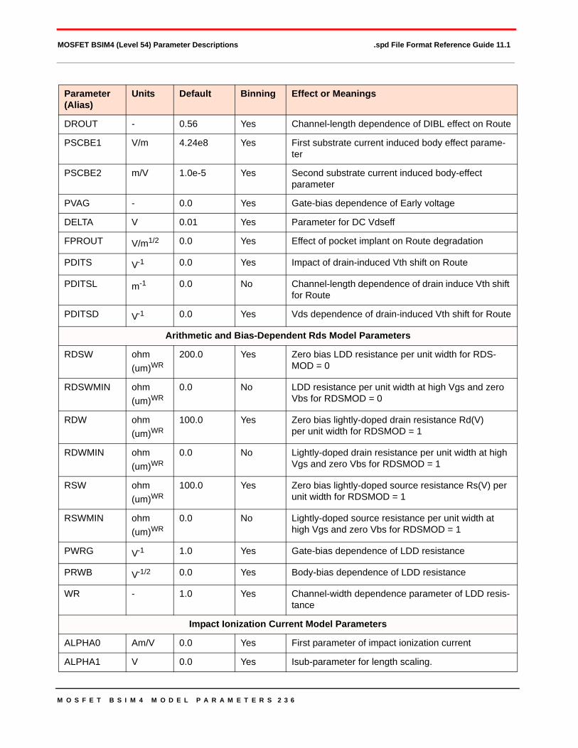
M O S F E T B S I M 4 M O D E L P A R A M E T E R S 2 3 6
MOSFET BSIM4 (Level 54) Parameter Descriptions .spd File Format Reference Guide 11.1
DROUT - 0.56 Yes Channel-length dependence of DIBL effect on Route
PSCBE1 V/m 4.24e8 Yes First substrate current induced body effect parame-ter
PSCBE2 m/V 1.0e-5 Yes Second substrate current induced body-effect parameter
PVAG - 0.0 Yes Gate-bias dependence of Early voltage
DELTA V 0.01 Yes Parameter for DC Vdseff
FPROUT V/m1/2 0.0 Yes Effect of pocket implant on Route degradation
PDITS V-1 0.0 Yes Impact of drain-induced Vth shift on Route
PDITSL m-1 0.0 No Channel-length dependence of drain induce Vth shift for Route
PDITSD V-1 0.0 Yes Vds dependence of drain-induced Vth shift for Route
Arithmetic and Bias-Dependent Rds Model Parameters
RDSW ohm (um)WR
200.0 Yes Zero bias LDD resistance per unit width for RDS-MOD = 0
RDSWMIN ohm (um)WR
0.0 No LDD resistance per unit width at high Vgs and zero Vbs for RDSMOD = 0
RDW ohm (um)WR
100.0 Yes Zero bias lightly-doped drain resistance Rd(V) per unit width for RDSMOD = 1
RDWMIN ohm (um)WR
0.0 No Lightly-doped drain resistance per unit width at high Vgs and zero Vbs for RDSMOD = 1
RSW ohm (um)WR
100.0 Yes Zero bias lightly-doped source resistance Rs(V) per unit width for RDSMOD = 1
RSWMIN ohm (um)WR
0.0 No Lightly-doped source resistance per unit width at high Vgs and zero Vbs for RDSMOD = 1
PWRG V-1 1.0 Yes Gate-bias dependence of LDD resistance
PRWB V-1/2 0.0 Yes Body-bias dependence of LDD resistance
WR - 1.0 Yes Channel-width dependence parameter of LDD resis-tance
Impact Ionization Current Model Parameters
ALPHA0 Am/V 0.0 Yes First parameter of impact ionization current
ALPHA1 V 0.0 Yes Isub-parameter for length scaling.
Parameter (Alias)
Units Default Binning Effect or Meanings

M O S F E T B S I M 4 M O D E L P A R A M E T E R S 2 3 7
MOSFET BSIM4 (Level 54) Parameter Descriptions .spd File Format Reference Guide 11.1
BETA0 V Version < = 4.40 30.0Version > = 4.50 0.0
Yes The second parameter of impact ionization current
Gate-Induced Drain Leakage Model Parameters
AGIDL mho 0.0 Yes Pre-exponential coefficient for GIDL
BGIDL V/m 2.3e-9 Yes Exponential coefficient for GIDL
OGIDL V3 0.5 Yes Parameter for body-bias effect on GIDL
EGIDL V 0.8 Yes Fitting parameter for band bending for GIDL
Gate Dielectric Tunneling Current Model Parameters
AIGBACC 1(Fs2/g)0.5m Version < 4.50 0.43Version > = 4.50 1.36e -2
Yes Parameter for Igb in accumulation
BIGBACC 1(Fs2g)0.5
m1V-1Version < 4.54 0.43Version > = 4.50 1.71e -3
Yes Parameter for Igb in accumulation
CIGBACC V-1 0.075 Yes Parameter for Igh in accumulation
NIGBACC - 1.0 Yes Parameter for Igh in accumulation
AIGBINV 1(Fs2g)0.5m- Version < 4.50 0.35Version > = 4.50 1.11e -2
Yes Parameter for Igh in inversion
BIGBINV (Fs2/g)0.5m-
1V-1Version < 4.50 0.03Version > = 4.50 9.49e -4
Yes Parameter for Igh in inversion
CIGBINV V-1 0.006 Yes Parameter for Igh in inversion
EIGBINV V 1.1 Yes Parameter for Igh in inversion
NIGVINV - 3.0 Yes Parameter for Igh in inversion
AIGC 1(Fs2g)0.5m- Version < = 4.40 0.43 (NMOS)0.31 (PMOS)Version > = 4.50 1.36e -3 (NMOS)7.50e -4 (PMOS)
Yes Parameter for Igcs and Igcd
Parameter (Alias)
Units Default Binning Effect or Meanings
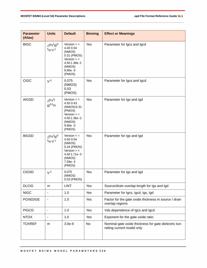
M O S F E T B S I M 4 M O D E L P A R A M E T E R S 2 3 8
MOSFET BSIM4 (Level 54) Parameter Descriptions .spd File Format Reference Guide 11.1
BIGC 1(Fs2g)0.
5m-V-1
Version < = 4.40 0.54 (NMOS)0.31 (PMOS)Version > = 4.50 1.36e -2 (NMOS) 9.80e -3 (PMOS)
Yes Parameter for lgcs and Igcd
CIGC V-1 0.075 (NMOS) 0.03 (PMOS)
Yes Parameter for Igcs and Igcd
AIGSD 1(Fs2/
g)0.5m
Version < = 4.50 0.43 (NMOS) 0.31 (PMOS) Version > = 4.50 1.36e -2 (NMOS)9.80e -3 (PMOS)
Yes Parameter for Igs and Igd
BIGSD 1(Fs2g)0.
5m-V-1
Version < = 4.50 0.54 (NMOS)0.24 (PMOS)Version > = 4.50 1.71e -3 (NMOS) 7.59e- 4 (PMOS)
Yes Parameter for Igs and Igd
CIGSD V-1 0.075 (NMOS) 0.03 (PMOS)
Yes Parameter for Igs and Igd
DLCIG m LINT Yes Source/drain overlap length for Igs and Igd
NIGC - 1.0 Yes Parameter for Igcs, Igcd, Igs, Igd
POXEDGE - 1.0 Yes Factor for the gate oxide thickness in source / drain overlap regions
PIGCD - 1.0 Yes Vds dependence of Igcs and Igcd
NTOX - 1.0 Yes Exponent for the gate oxide ratio
TOXREF m 3.0e-9 No Nominal gate oxide thickness for gate dielectric tun-neling current model only
Parameter (Alias)
Units Default Binning Effect or Meanings

M O S F E T B S I M 4 M O D E L P A R A M E T E R S 2 3 9
MOSFET BSIM4 (Level 54) Parameter Descriptions .spd File Format Reference Guide 11.1
Charge and Capacitance Model Parameters
XPART - 0.0 No Charge partition parameter
CGSO F/m Calculated No Non LDD region source-gate overlap capacitance per unit channel width
CGDO F/m Calculated No Non LDD region drain-gate overlap capacitance per unit channel width
CGBO F/m 0.0 No Gate-bulk overlap capacitance per unit channel length
CGSL F/m 0.0 Yes Overlap capacitance between gate and lightly-doped source region
CGDL F/m 0.0 Yes Overlap capacitance between gate and lightly-doped source region
CKAPPAS V 0.6 Yes Coefficient of bias-dependent overlap capacitance for the source side
CKAPPAD V CKAPPAS Yes Coefficient of bias-dependent overlap capacitance for the drain side
CF F/m Calculated Yes Coefficient of bias-dependent overlap capacitance for the drain side
CLC m 1.0e-7 Yes Fringing field capacitance
CLE - 0.6 Yes Constant term for the short channel model
DLC m LINT No Channel-length offset parameter for CV model
DWC m WINT No Channel-width offset parameter for CV model
VFBCV V -1.0 Yes Flat-band voltage parameter (for CAPMOD=0 only)
NOFF - 1.0 Yes CV parameter in VgsteffFor weak to strong inversion
VOFFCV V 0.0 Yes CV parameter in VgsteffFor weak to strong inversion
ACDE m/V 1.0 Yes Exponential coefficient for charge thickness in CAP-MOD=2 for accumulation and depletion regions
MOIN - 15.0 Yes Coefficient for the gate-bias dependent surface potential
High-Speed/RF Model Parameters
XRCRG1 - 12.0 Yes Parameter for distributed channel resistance effect for both intrinsic input resistance and charge-deficit NQS models
Parameter (Alias)
Units Default Binning Effect or Meanings
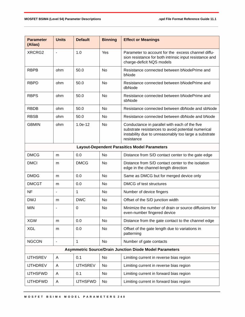
M O S F E T B S I M 4 M O D E L P A R A M E T E R S 2 4 0
MOSFET BSIM4 (Level 54) Parameter Descriptions .spd File Format Reference Guide 11.1
XRCRG2 - 1.0 Yes Parameter to account for the excess channel diffu-sion resistance for both intrinsic input resistance and charge-deficit NQS models
RBPB ohm 50.0 No Resistance connected between bNodePrime and bNode
RBPD ohm 50.0 No Resistance connected between bNodePrime and dbNode
RBPS ohm 50.0 No Resistance connected between bNodePrime and sbNode
RBDB ohm 50.0 No Resistance connected between dbNode and sbNode
RBSB ohm 50.0 No Resistance connected between dbNode and bNode
GBMIN ohm 1.0e-12 No Conductance in parallel with each of the five substrate resistances to avoid potential numerical instability due to unreasonably too large a substrate resistance
Layout-Dependent Parasitics Model Parameters
DMCG m 0.0 No Distance from S/D contact center to the gate edge
DMCI m DMCG No Distance from S/D contact center to the isolation edge in the channel-length direction
DMDG m 0.0 No Same as DMCG but for merged device only
DMCGT m 0.0 No DMCG of test structures
NF - 1 No Number of device fingers
DWJ m DWC No Offset of the S/D junction width
MIN - 0 No Minimize the number of drain or source diffusions for even-number fingered device
XGW m 0.0 No Distance from the gate contact to the channel edge
XGL m 0.0 No Offset of the gate length due to variations in patterning
NGCON - 1 No Number of gate contacts
Asymmetric Source/Drain Junction Diode Model Parameters
IJTHSREV A 0.1 No Limiting current in reverse bias region
IJTHDREV A IJTHSREV No Limiting current in reverse bias region
IJTHSFWD A 0.1 No Limiting current in forward bias region
IJTHDFWD A IJTHSFWD No Limiting current in forward bias region
Parameter (Alias)
Units Default Binning Effect or Meanings

M O S F E T B S I M 4 M O D E L P A R A M E T E R S 2 4 1
MOSFET BSIM4 (Level 54) Parameter Descriptions .spd File Format Reference Guide 11.1
XJBVS - 1.0 No Fitting parameter for diode breakdown
XJBVD - XJBVS No Fitting parameter for diode breakdown
BVS V 10.0 No Breakdown voltage
BVD V BVS No Breakdown voltage
JSS A/m2 1.0e-4 No Bottom junction reverse saturation current density
JSD A/m2 JSS No Bottom junction reverse saturation current density
JSWS A/m 0.0 No Isolation-edge sidewall reverse saturation current density
JSWD A/m JSWS No Isolation-edge sidewall reverse saturation current density
JSWGS A/m 0.0 No Gate-edge sidewall reverse saturation current den-sity
JSWGD A/m JSWGS No Gate-edge sidewall reverse saturation current density
CJS F/m2 0.0 No Bottom junction capacitance per unit area at zero bias
CJD F/m2 CJS No Bottom junction capacitance per unit area at zero bias
MJS - 0.5 No Bottom junction capacitance grating coefficient
MJD - MJS No Bottom junction capacitance grating coefficient
MJSWS - 0.33 No Isolation-edge sidewall junction capacitance grading coefficient
MJSWD - MJSWS No Isolation-edge sidewall junction capacitance grading coefficient
MJSWGS - MJSWS No Gate-edge side wall junction capacitance grading coefficient
MJSWGD - MJSWS No Gate-edge sidewall junction capacitance grading coefficient
CJSWS F/m 5.0e-10 No Isolation-edge sidewall junction capacitance per unit area
CJSWD F/m CJSWS No Isolation-edge sidewall junction capacitance per unit area
CJSWGS F/m CJSWS No Gate-edge sidewall junction capacitance per unit length
Parameter (Alias)
Units Default Binning Effect or Meanings

M O S F E T B S I M 4 M O D E L P A R A M E T E R S 2 4 2
MOSFET BSIM4 (Level 54) Parameter Descriptions .spd File Format Reference Guide 11.1
CJSWGD F/m CJSWS No Gate-edge sidewall junction capacitance per unit length
PBS V 1.0 No Bottom junction built-in potential
PBD V PBS No Bottom junction built-in potential
PBSWS V 1.0 No Isolation-edge sidewall junction built-in potential
PBSWD V PBSWS No Isolation-edge sidewall junction built-in potential
PBSWGS V PBSWS No Isolation-edge sidewall junction built-in potential
PBSWGD PBSWS No Isolation-edge sidewall junction built-in potential
Temperature Dependence Parameters
TNOM (TREF)
oC 27 No Temperature at which parameters are extracted
UTE - -1.5 Yes Mobility temperature exponent
KT1 V -0.11 Yes Temperature coefficient for threshold
KT1L Vm 0.0 Yes Channel length dependence of the temperature coefficient for threshold voltage
KT2 - 0.022 Yes Body-bias coefficient of Vth temperature effect
UA1 m/V 1.0e-9 Yes Temperature coefficient for UA.
UB1 (m/V)2 -1.0e-18 Yes Temperature coefficient for UB
UC1 V-1
m/V2
0.067 (MO BMOD = 1)0.025 (MO BMOD = 0.2)
Yes Temperature coefficient for UC
AT m/s 3.3e4 Yes Temperature coefficient for saturation velocity
PRT ohm*m 0.0 Yes Temperature coefficient for Rdsw
NJS - 1.0 Yes Emission coefficients of junction for source junction
NJD - NJS No Emission coefficients of junction for drain junction
XTIS - 3.0 No Junction current temperature exponents fro source junction
XTID - XTIS No Junction current temperature exponents for drain junction
TPB V/K 0.0 No Temperature coefficient of PB
TPBSW V/K 0.0 No Temperature coefficient of PBSW
TPBSWG V/K 0.0 No Temperature coefficient of PBSWG
Parameter (Alias)
Units Default Binning Effect or Meanings
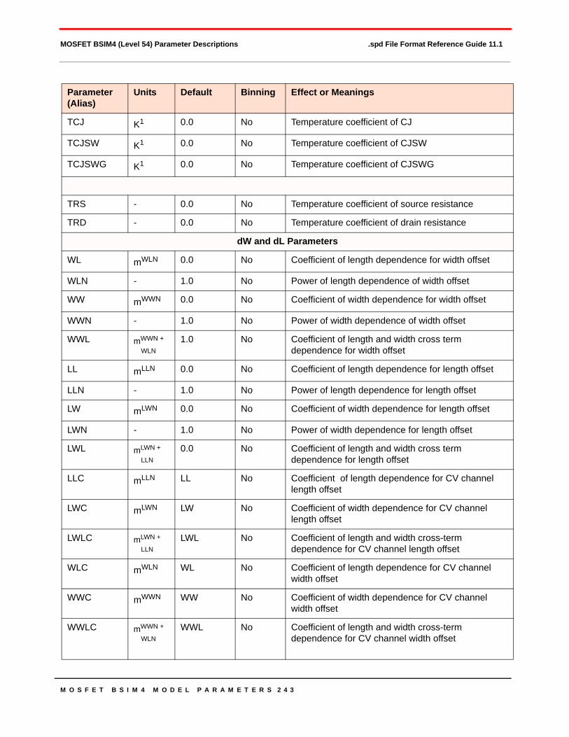
M O S F E T B S I M 4 M O D E L P A R A M E T E R S 2 4 3
MOSFET BSIM4 (Level 54) Parameter Descriptions .spd File Format Reference Guide 11.1
TCJ K1 0.0 No Temperature coefficient of CJ
TCJSW K1 0.0 No Temperature coefficient of CJSW
TCJSWG K1 0.0 No Temperature coefficient of CJSWG
TRS - 0.0 No Temperature coefficient of source resistance
TRD - 0.0 No Temperature coefficient of drain resistance
dW and dL Parameters
WL mWLN 0.0 No Coefficient of length dependence for width offset
WLN - 1.0 No Power of length dependence of width offset
WW mWWN 0.0 No Coefficient of width dependence for width offset
WWN - 1.0 No Power of width dependence of width offset
WWL mWWN +
WLN1.0 No Coefficient of length and width cross term
dependence for width offset
LL mLLN 0.0 No Coefficient of length dependence for length offset
LLN - 1.0 No Power of length dependence for length offset
LW mLWN 0.0 No Coefficient of width dependence for length offset
LWN - 1.0 No Power of width dependence for length offset
LWL mLWN +
LLN0.0 No Coefficient of length and width cross term
dependence for length offset
LLC mLLN LL No Coefficient of length dependence for CV channel length offset
LWC mLWN LW No Coefficient of width dependence for CV channel length offset
LWLC mLWN +
LLNLWL No Coefficient of length and width cross-term
dependence for CV channel length offset
WLC mWLN WL No Coefficient of length dependence for CV channel width offset
WWC mWWN WW No Coefficient of width dependence for CV channel width offset
WWLC mWWN +
WLNWWL No Coefficient of length and width cross-term
dependence for CV channel width offset
Parameter (Alias)
Units Default Binning Effect or Meanings

M O S F E T B S I M 4 M O D E L P A R A M E T E R S 2 4 4
MOSFET BSIM4 (Level 54) Parameter Descriptions .spd File Format Reference Guide 11.1
LMLT - 1.0 No Channel length multiplier
WMLT - 1.0 No Channel width multiplier
Range Parameters for Model Applications
LMIN m 0.0 No Minimum channel length
LMAX m 1.0 No Maximum channel length
WMIN m 0.0 No Minimum channel width
WMAX m 0.0 No Maximum channel width
BSIM4.2.0 Introduced Model Parameters
XL m 0.0 No Channel length offset due to mask / etch effect
XW m 0.0 No Channel width offset due to mask / etch effect
BSIM4.3.0 Introduces Model Parameters
TEMPMOD - 0 No Temperature mode selector
LAMBDA - 0.0 Yes Velocity overshoot coefficient
VTL m/s 2.05e5 Yes Thermal velocity
LC m 0.0 No Velocity back scattering coefficient
XN - 3.0 Yes Velocity back scattering coefficient
BSIM4.3.0 Introduced - Stress Effect Model Parameters
SAREF m 1.0e-6 No Reference distance between OD and edge to poly of one side
SBREF m 1.0e-6 No Reference distance between OD and edge to poly of the other side
WLOD m 0.0 No Width parameter for stress effect
KUO m 0.0 No Mobility degradation / enhancement coefficient for stress effect
KVSAT m 0.0 No Saturation velocity degradation / enhancement parameter for stress effect
TKU0 - 0.0 No Temperature coefficient of KU0
LKU0 - 0.0 No Length dependence of ku0
WKU0 - 0.0 No Width dependence of ku0
Parameter (Alias)
Units Default Binning Effect or Meanings
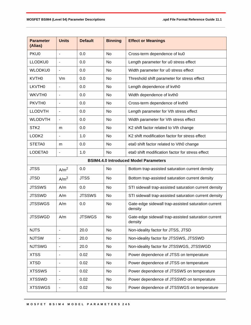
M O S F E T B S I M 4 M O D E L P A R A M E T E R S 2 4 5
MOSFET BSIM4 (Level 54) Parameter Descriptions .spd File Format Reference Guide 11.1
PKU0 - 0.0 No Cross-term dependence of ku0
LLODKU0 - 0.0 No Length parameter for u0 stress effect
WLODKU0 - 0.0 No Width parameter for u0 stress effect
KVTH0 Vm 0.0 No Threshold shift parameter for stress effect
LKVTH0 - 0.0 No Length dependence of kvth0
WKVTH0 - 0.0 No Width dependence of kvth0
PKVTH0 - 0.0 No Cross-term dependence of kvth0
LLODVTH - 0.0 No Length parameter for Vth stress effect
WLODVTH - 0.0 No Width parameter for Vth stress effect
STK2 m 0.0 No K2 shift factor related to Vth change
LODK2 - 1.0 No K2 shift modification factor for stress effect
STETA0 m 0.0 No eta0 shift factor related to Vth0 change
LODETA0 - 1.0 No eta0 shift modification factor for stress effect
BSIM4.4.0 Introduced Model Parameters
JTSS A/m2 0.0 No Bottom trap-assisted saturation current density
JTSD A/m2 JTSS No Bottom trap-assisted saturation current density
JTSSWS A/m 0.0 No STI sidewall trap-assisted saturation current density
JTSSWD A/m JTSSWS No STI sidewall trap-assisted saturation current density
JTSSWGS A/m 0.0 No Gate-edge sidewall trap-assisted saturation current density
JTSSWGD A/m JTSWGS No Gate-edge sidewall trap-assisted saturation current density
NJTS - 20.0 No Non-ideality factor for JTSS, JTSD
NJTSW - 20.0 No Non-ideality factor for JTSSWS, JTSSWD
NJTSWG - 20.0 No Non-ideality factor for JTSSWGS, JTSSWGD
XTSS - 0.02 No Power dependence of JTSS on temperature
XTSD - 0.02 No Power dependence of JTSS on temperature
XTSSWS - 0.02 No Power dependence of JTSSWS on temperature
XTSSWD - 0.02 No Power dependence of JTSSWD on temperature
XTSSWGS - 0.02 No Power dependence of JTSSWGS on temperature
Parameter (Alias)
Units Default Binning Effect or Meanings
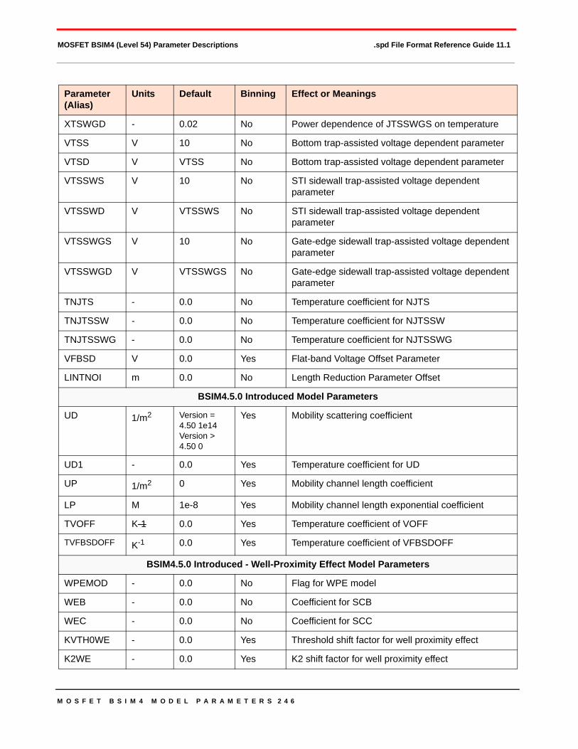
M O S F E T B S I M 4 M O D E L P A R A M E T E R S 2 4 6
MOSFET BSIM4 (Level 54) Parameter Descriptions .spd File Format Reference Guide 11.1
XTSWGD - 0.02 No Power dependence of JTSSWGS on temperature
VTSS V 10 No Bottom trap-assisted voltage dependent parameter
VTSD V VTSS No Bottom trap-assisted voltage dependent parameter
VTSSWS V 10 No STI sidewall trap-assisted voltage dependent parameter
VTSSWD V VTSSWS No STI sidewall trap-assisted voltage dependent parameter
VTSSWGS V 10 No Gate-edge sidewall trap-assisted voltage dependent parameter
VTSSWGD V VTSSWGS No Gate-edge sidewall trap-assisted voltage dependent parameter
TNJTS - 0.0 No Temperature coefficient for NJTS
TNJTSSW - 0.0 No Temperature coefficient for NJTSSW
TNJTSSWG - 0.0 No Temperature coefficient for NJTSSWG
VFBSD V 0.0 Yes Flat-band Voltage Offset Parameter
LINTNOI m 0.0 No Length Reduction Parameter Offset
BSIM4.5.0 Introduced Model Parameters
UD 1/m2 Version = 4.50 1e14Version > 4.50 0
Yes Mobility scattering coefficient
UD1 - 0.0 Yes Temperature coefficient for UD
UP 1/m2 0 Yes Mobility channel length coefficient
LP M 1e-8 Yes Mobility channel length exponential coefficient
TVOFF K-1 0.0 Yes Temperature coefficient of VOFF
TVFBSDOFF K-1 0.0 Yes Temperature coefficient of VFBSDOFF
BSIM4.5.0 Introduced - Well-Proximity Effect Model Parameters
WPEMOD - 0.0 No Flag for WPE model
WEB - 0.0 No Coefficient for SCB
WEC - 0.0 No Coefficient for SCC
KVTH0WE - 0.0 Yes Threshold shift factor for well proximity effect
K2WE - 0.0 Yes K2 shift factor for well proximity effect
Parameter (Alias)
Units Default Binning Effect or Meanings
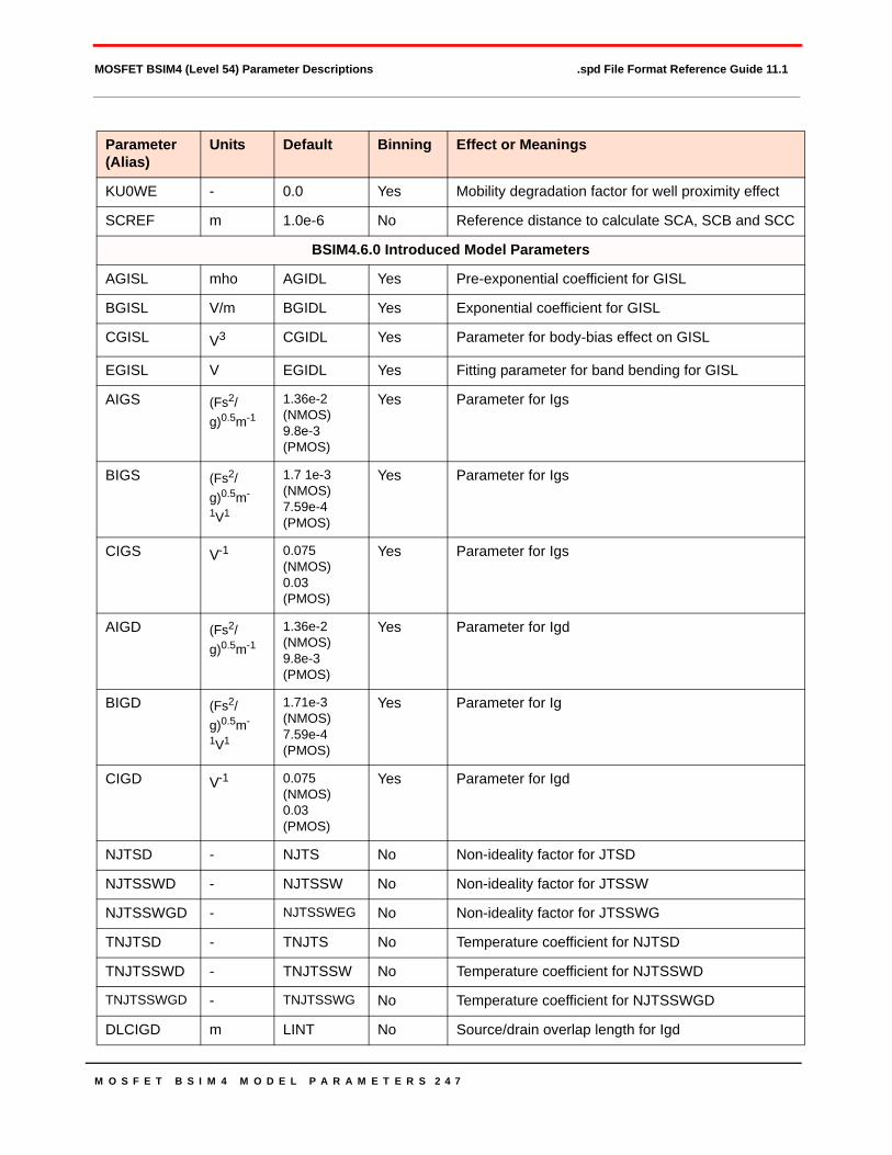
M O S F E T B S I M 4 M O D E L P A R A M E T E R S 2 4 7
MOSFET BSIM4 (Level 54) Parameter Descriptions .spd File Format Reference Guide 11.1
KU0WE - 0.0 Yes Mobility degradation factor for well proximity effect
SCREF m 1.0e-6 No Reference distance to calculate SCA, SCB and SCC
BSIM4.6.0 Introduced Model Parameters
AGISL mho AGIDL Yes Pre-exponential coefficient for GISL
BGISL V/m BGIDL Yes Exponential coefficient for GISL
CGISL V3 CGIDL Yes Parameter for body-bias effect on GISL
EGISL V EGIDL Yes Fitting parameter for band bending for GISL
AIGS (Fs2/g)0.5m-1
1.36e-2(NMOS)9.8e-3(PMOS)
Yes Parameter for Igs
BIGS (Fs2/g)0.5m-
1V1
1.7 1e-3(NMOS)7.59e-4(PMOS)
Yes Parameter for Igs
CIGS V-1 0.075(NMOS)0.03(PMOS)
Yes Parameter for Igs
AIGD (Fs2/g)0.5m-1
1.36e-2(NMOS)9.8e-3(PMOS)
Yes Parameter for Igd
BIGD (Fs2/g)0.5m-
1V1
1.71e-3(NMOS)7.59e-4(PMOS)
Yes Parameter for Ig
CIGD V-1 0.075(NMOS)0.03(PMOS)
Yes Parameter for Igd
NJTSD - NJTS No Non-ideality factor for JTSD
NJTSSWD - NJTSSW No Non-ideality factor for JTSSW
NJTSSWGD - NJTSSWEG No Non-ideality factor for JTSSWG
TNJTSD - TNJTS No Temperature coefficient for NJTSD
TNJTSSWD - TNJTSSW No Temperature coefficient for NJTSSWD
TNJTSSWGD - TNJTSSWG No Temperature coefficient for NJTSSWGD
DLCIGD m LINT No Source/drain overlap length for Igd
Parameter (Alias)
Units Default Binning Effect or Meanings
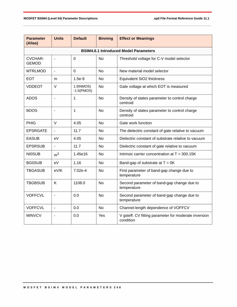
M O S F E T B S I M 4 M O D E L P A R A M E T E R S 2 4 8
MOSFET BSIM4 (Level 54) Parameter Descriptions .spd File Format Reference Guide 11.1
BSIM4.6.1 Introduced Model Parameters
CVCHAR-GEMOD
- 0 No Threshold voltage for C-V model selector
MTRLMOD - 0 No New material model selector
EOT m 1.5e-9 No Equivalent SiO2 thickness
VDDEOT V 1.5INMOS)-1.5(PMOS)
No Gate voltage at which EOT is measured
ADOS - 1 No Density of states parameter to control charge centroid
BDOS - 1 No Density of states parameter to control charge centroid
PHIG V 4.05 No Gate work function
EPSRGATE - 11.7 No The dielectric constant of gate relative to vacuum
EASUB eV 4.05 No Dielectric constant of substrate relative to vacuum
EPSRSUB - 11.7 No Dielectric constant of gate relative to vacuum
NI0SUB m3 1.45e16 No Intrinsic carrier concentration at T = 300.15K
BG0SUB eV 1.16 No Band-gap of substrate at T = 0K
TBGASUB eV/K 7.02e-4 No First parameter of band-gap change due to temperature
TBGBSUB K 1108.0 No Second parameter of band-gap change due to temperature
VOFFCVL - 0.0 No Second parameter of band-gap change due to temperature
VOFFCVL - 0.0 No Channel-length dependence of VOFFCV
MINVCV - 0.0 Yes V gsteff. CV fitting parameter for moderate inversion condition
Parameter (Alias)
Units Default Binning Effect or Meanings
Index 2 4 9
Index .spd File Format Reference Guide 11.1
IndexSymbols_Cmatrix 56, 127_Cmatrix statement 135_Lmatrix 56, 123_LMatrix Indicator Example 1 123. 13, 34.Connect 70.Connect keyword 70.Connect line 70.DielectricModel 34.DiffChannels 173.Distribution 161.End 5.End statement 5.EndC 70, 216.EndC line 70.EndDielectricModel 34.EndDiffChannels 173.EndMaterial 34.EndMetalModel 34.EndPort 172.EndPowerSI 168, 169.EndShape 6, 15, 16.EndThermalModel 34.ExternalCircuitSolver statement 216.Material 34.Mesh line 12.MetalModel 34.Model 20.NetList 173.Output3D 161.Output3DCurrent 162.Output3DVoltage 161.Param 64.Param lines 63.Partial 64.PartialCkt 64, 71.Port 172.PowerSI 169.Shape 15.spd data file 3.spd file 135, 173.SPD File Example 3.spd file format 1.SubCkt 64.SUBCKT command 67, 96.Subckt definitions 71.Subckt statements 64.TEMP statement 135.ThermalModel 34.Transient line 9.View3D 159, 161.ViewCktVoltage 157.ViewCurrent 159
.ViewPkgVoltage 158"+" 3
Aabs(x) 58ABS=1 108Absent 70absolute path 217, 218absolute rotation 37absolute value 61, 120Absolute value function 58AC arguments 121AC source keyword 121AC voltage 121ACM 89ACM>1 83acos(x) 58Adaptive 171Adaptive sweeping 171adaptive sweeping 171adaptive type sweeping 170add IBIS file 213adjacent bits 140, 142Adjustment ratio 22, 29Adjustment ratio of distributed
resistance 22Admittance 4Admittance parameter 167Affix 54Aliases mapping 133Alpha 44ALPHA length sensitivity 87ALPHA width sensitivity 87Alphabetical characters 5Amplitude 161AND 118appropriate IBIS file 213APWARN 89Arc cosine function 58Arc sine function 58Arc tangent function 58Area factor 101AreaAdj 29AreaAdj option 22, 27As Error 6As Warning 6ASCII 3asin(x) 58asterisk 5atan(x) 58auto-coupled 164automatic circuit selection
procedure 156
BB 56Backupshape 6BackupUnionizedShape 6Backward Euler’s 10bandgap correction factor 75Band-gap of substrate 248Base 10 logarithm function 58base frequency 80, 129Berkeley junction diode 76bias depletion capacitance
coefficient 82Bias-dependent source/drain
resistance model 232BINFLAG 89Binning unit selector 232bit before the edge 142Bit period 152bit with pattern value 0 140Bits File Format 152Bits File Format Example 152blank line 3blank space 3bNode 93, 240bNodePrime 93, 240BNP 129, 168BNP file name 80body bias 221, 234body bias coefficient 222body effect coefficient 221Body effect factor 86Body-bias coefficient 222, 229, 235Body-effect coefficient 221, 233Bottom junction reverse
saturation 241Bottom trap-assisted saturation
current density 245Bottom trap-assisted voltage 246box color 16Box keyword 16Box parameter 16Box Parameter Example 16Branch number 124Branch Parameters 124branches 124BSIM3v3 88, 231BSIM4 92, 232Buffer state 186buffer state 187, 196buffer switch 189, 191, 193Bulk charge 222Bulk charge effect 222Bulk Junction saturation current 81
Index 2 5 0
Index .spd File Format Reference Guide 11 .1
Bulk junction saturation current 90, 224
Bulk node 126Bulk surface doping 86Bulk to Source/Drain Diodes 81
CC 56, 98C_comp value 181CALCACM 89Capacitance 4capacitance matrix 79Capacitance model selector 219, 232Capacitance multiplier 84Capacitance Part Parameters 82Capacitance value 136capacitor 56, 98, 99capacitor element 97Capacitor Example 98Capacitor Parameters 99capacitors 209CAPMOD 226Carrier frequency 144cartesian coordinate system 12CCCS 56, 107CCCS Parameters 108CCVS 56, 119CCVS Parameters 120CDSC 223CGB exponent 84Channel doping 233Channel doping concentration 221channel edge 240Channel length 90channel length 221, 227Channel length modulation 231Channel length multipler 244Channel length reduction 85, 90Channel length reference 85channel pocket devices 234Channel width 228Channel width reference 85Channel-length dependence 235, 236character string 61, 62, 69, 108, 131,
180character string for the name of the
output file 161Characteristic impedance 130charge thickness 226Circle key word 18Circle Parameter 18Circle parameter 18Circle Parameter Example 18Circuit
format 55circuit components 55circuit definition 64
Circuit description 123circuit element definition 68circuit network 55circuit node 61, 109, 113circuit node connected 62, 125circuit node connected to one end of
the inductor 62circuit nodes 116circuit not considered in
simulation 70circuit temperature 126Circuit-Package 209CJ 226CJSW 226CJSWG 229ClippedTrace 48ClippedTrace Example 48cload definition scope 97cmat.dat file 135, 136Cmatrix 100coefficient for R 77Coefficient of first-order mobility
degradation 234Color 54Color intensity plot 160comma separated list 140Comment lines 5comment lines 3, 5commonly-used commands 218Component parameter 182component pins 65ComponentName field 65components inside the box 191computation and display 165computation parameter lines 9Conductance 240Conductivity 22, 23, 26, 29, 31, 39, 47,
52, 54conductivity parameter 39Connection lines 70connections 70connector definition 97Contact 37contact resistance 83controlled component 57controlled current source 103, 108,
109, 111controlled currents 108, 116controlled resistor 118controlled source
CCCS 107CCVS 119VCCS 61, 114, 115VCR 61, 117, 118VCVS 104
controlled voltage source 102, 120controlling current flows 108, 120
controlling the buffer state 188controlling variables 57controlling voltage 111, 115controlling voltages 105, 116cos(x) 58cosh(x) 58Cosine function 58coupled inductor 122coupled line object 49coupled lossless lines 132coupled lossy lines 132coupled traces 48Coupled Transmission Line
Description Line 132Coupled Transmission
Parameters 132Coupling capacitance 235Coupling coefficient 122coupling coefficient L of
inductors 124coupling lines 49CPL 20, 48create a new partial circuit
definition 213Critical voltage 87Cross-term dependence 91, 245Current 4Current controlled current source 56current controlled current source 108current controlled voltage source 119current file 217Current flows 59current flows into the current
source 121current flows out of the current
source 121Current gain 108current source 56, 108, 121Current Source Example 121Current Source Parameters 121current sources 121current variable 59Current Variable Example 59CV model 239
DDamping factor 150data block 63data file 135data file in disk 124Data file name 129data section enclosed by
.HSPICE 216data sections for an IBIS file 178data selected 180dbNode 240DC analysis 10, 62

Index 2 5 1
Index .spd File Format Reference Guide 11.1
DC model selector 231DC Parameters 92, 221DC Resistance 130DC voltages 162Default Fbase 80, 129default locations with default
sizes 165Default resistance 77define each port 172defined variable name 98degradation coefficient 222degradation/enhancement
coefficient 244Delay 107Delay Key function 105, 108, 115, 120deltai 116DELVTO 86depletion junction 74depletion region 221determining buffer state 194determining the buffer state 186device model calculation 12device model simulation options 134device models 218DIBL coefficient 223DIBL coefficient exponent 235die capacitance 181Dielectric constant of substrate
relative to vacuum 248Dielectric loss 79dielectric loss 11, 132dielectric medium 26dielectric model 26DielectricLossDispersion 11DieName 45Diff_Channel_xxxx_$_yyyy 173Diff_Channel_xxxx_$_yyyy
Example 173different lead models 53Differential channel ports 173Diffusion layer 228digital logic thresholds 209Digital output signal 184digital signal 184, 190digital signal controlled by
voltage 202digital waveform 152dimension 120Diode 56, 73diode 20Diode Description Line 100Diode Example 100Diode initial voltage 101diode is OFF 101Diode limiting current 224diode model 101diode model parameter PJ 101
Diode model selector 73Diode name 101Diode Parameters 101DISABLE 187discretized wirebond model 44dispersion 11displaying the mesh 160distributed admittance 27distributed resistance 22distribution of peak or average
voltage magnitude 157DMCG of test structures 240Dogleg Hole 7doped diffusion 224doped source-gate region 226Doping depth 221, 233Drain and Source Resistance
Parameters 83drain diffusion for resistance
calculations 126drain junction 126Drain node 126drain or source diffusions 93, 240Drain resistance 83, 90, 224drain resistance 224Drain/Source to channel 223Drain-bias 223drain-gate overlap capacitance 225drain-gate region 226drawn and actual width 77
EE 56, 104E type components 116ECL buffer 202, 204edit an existing definition 213Effective Length and Width
Parameters 85effective scope 64electric contact 37electrical net 164element current curves 165element temperature 126, 135elements in parallel 61, 108, 115Emission coefficient 74, 81, 90, 224Emission coefficients of junction for
drain junction 242ENABLE 187Enable 214ENABLE signal 188, 190, 197enable signal for the pin 65Enable values 187EnableSignal 65end line 5End Line Example 6end lines 5ending frequency 171
EndingNode 45, 47, 54Energy gap 75Er 52ertical height of the segment 44Eta0 91Eta0 shift factor 230Eta0 shift modification factor 91Example of Signal Layer 25executable modules 19EXP 143exp(x) 58explosion parameter 73Exponent for mobility degration 234Exponential coefficient 237, 239Exponential function 57, 58expression 60expressions 62external circuit solver 216external circuit solvers 216external drain and source 126ExtNode 69
FF 56, 107Fall 143falling curves 180falling ramp data 180Falling time 152falling waveforms 180far-end reference-conductor
terminal 132far-end signal-conductor
terminal 132FDG 132field solver module 20, 25, 28Fields 213file path 217, 218Finaltime 10first parameter 168, 179Fitting parameter for band
bending 247flat band voltage 221Flat-band voltage 233Flatband Voltage Offset
Parameter 246Fmax_TransmissionLine 11Foster Pole-Residue form gain
function 102Foster Pole-Residue form Trans-
conductance function 109Fourier Transform 129fractions 181free Node 44free segment 44freq 60Frequency increment 170frequency increment 171
Index 2 5 2
Index .spd File Format Reference Guide 11 .1
Frequency Piecewise Linear Waveform Example 174
frequency simulation parameters 170Frequency Sweep Example 1 170Frequency Sweep Example 2 170Frequency-Modulated
Waveform 148FrequencySweep line 170Fringing field 226Fringing field capacitance 239Fringing field factor 84
GG 56, 109G and E components 60G and E Parameters 61G and E type components 61G element key word 61gain function 102Gain Function Example 102GAMMA 86Gate bias coefficient 222Gate bias effect 222Gate bulk overlap 225Gate Capacitances Parameters 84gate contacts 93Gate dependence 222Gate dielectric 233Gate electrode sheet resistance 233Gate length shrink factor 85, 90gate material 86Gate node 126Gate oxide thickness 221gate oxide thickness 238Gate resistance 232Gate resistance model selector 93Gate work function 248Gate-bias dependence of Early
voltage 236gate-bias dependent 226Gate-bulk overlap capacitance 84Gate-drain overlap capacitance 84Gate-edge sidewall trap-assisted
saturation 245Gate-source overlap capacitance 84Gate-to-channel tunneling 232GCPL 20GCPL description 48GCPL Description Block 49GCPL Illustration 49GEAR 134General Form for LeadGroup 54General Form for Material
Section 34General Form for PowerSI 130General Form for SPDSIM 130
general forms for current controlled current source 107
general forms for VCCAP 112general forms for VCCS 114general forms for VCR 117Geometry-dependent parasitics
model selector 232GIDL 237Global defined parameters 97global defined parameters 68global parameter 64global parameter specification 69, 98Global Parameters 64global parameters 60gnd 202GPL 20Grading coefficien 74ground clamp 184, 186, 188, 192Ground node 184, 186, 188, 192Gy 116
HH 56, 114HDIFscaled 83heavily-doped diffusion 83horizontal distance 44horizontal xis 44HSPICE 69, 180, 216HSPICE circuit solvers 216Hyperbolic cosine function 58Hyperbolic tangent function 58
II 56, 137I/O Buffer Illustration 189I/O Open 201I/O open drain buffer 194I/O Open Sink buffer 197I/O type buffer 190, 197IBIS 177IBIS committee 177IBIS component 213IBIS components 65IBIS file 65, 178, 180, 213IBIS file name 65IBIS I/O Buffer 189IBIS I/O ECL Buffer 207IBIS I/O ECL Buffer Illustration 207IBIS I/O Open Drain Buffer 192IBIS I/O Open Drain Buffer
Illustration 193IBIS I/O Open Sink Buffer 196IBIS I/O Open Sink Buffer
Illustration 197IBIS I/O Open Source Buffer 200IBIS I/O Open Source Buffer
Illustration 200
IBIS Input Buffer 182IBIS Input Buffer Illustration 183IBIS Input ECL Buffer 202, 203IBIS Input ECL Buffer
Illustration 202IBIS models 56IBIS Open Drain 191IBIS Open Drain Buffer
Illustration 191IBIS Open Sink Buffer 195IBIS Open Sink Buffer
Illustration 195IBIS Open Source Buffer
Illustration 198IBIS Out ECL Buffer Illustration 204IBIS Output Buffer 185IBIS Output ECL Buffer 203IBIS Terminator Buffer
Illustration 209IBIS Tristate Buffer 187IBIS Tristate Buffer Illustration 187IBIS Tristate ECL Buffer 205IBIS Tristate ECL Buffer
Illustration 205IC 115Ideal threshold voltage 221Ideal transformer 105identical partial circuit networks 55Igb 237Igcd 237Igcs 237Igd 238Igh 237Igs 238Im 162Imag(X) 102, 109imagine part of X 102, 109Imagnitude 162Impact ionization 87impact ionization 223Impact ionization coefficient 87Impact Ionization Parameters 87Impedance parameter 167INCLUDERSIMAG 132independent voltage source 59Inductance 4, 125inductance 122inductor 124, 125Inductor L11 122Inductor L18 122Inductor Matrix Description
Line 123industry-standard MOSFET
model 92Initial condition 105, 108Initial current 62Initial value 143, 145

Index 2 5 3
Index .spd File Format Reference Guide 11.1
initial value 168, 179Inner resistance 131InnerRadius 31input buffer. 190input data file 5Input logic 184input node 197input-only model 209Interface trap capacitance 223, 235IntMethod 10Intrinsic carrier concentration 248Intrinsic transconductance
parameter 231IOBufferD 67, 96ionization current 236isolation edge 240Isolation-edge sidewall junction 242Isolation-edge sidewall junction
capacitance 241Isub parameter for length scaling 236Ix 162Iy 162
JJunction Area 73Junction depth 221junction periphery 74
KK 56K2 shift factor 245K2 shift modification 230Keywords 157keywords 178Keywords of package layout lines 20knee current 73KU0 91, 230KVTH0 230
LL 56, 98L_low 52L_up 52Laplace 103, 110Laplace and Pole-zero Trans-
conductance Function 110Laplace and Pole-zero Voltage Gain
Function 102last effective line 5Lateral diffusion 85Lateral non-uniform doping
effect 234Lateral non-uniform doping
parameter 221Layers 20layers of the package structure 165Lead data 50
Lead Group Section 54Lead Model Example 51LeadGroup 54LeadGroup Example 54LeadGroup Name 54LeadModel 52LeadType_1 53LeadType_2 53LeadType_3 53LeadType_4 53Length 4, 128Length bias 85, 228length dependence 227length of the name 5Length offset 222Length scaling parameter 223less than two pairs 106Letter “I” 59level 49 88Level 53 88, 92level 54 92library file is not found 218library files 218lightly-doped diffusion 90L-Inductor Example 124line types 5Linear 104, 107Linear sweeping 171linear sweeping 171linked with the triggering signal 194linking the two terminals 44Lmatrix 123L-Matrix Indicator Example 2 123Local and global defined
parameters 57local and global parameter 63local defined parameters 68, 97local parameter 63, 64local parameter name 98Local parameter specification 69, 98local parameter specification 69, 98Local parameters 64local variables 94location of the .spd file 217location of the current file 217log(x) 58log10(x) 58Logarithmic sweeping 171Loss Tangent and Conductivity 26LossTangent 26lower layer 158lower reference plane 47lower-level circuit and elements 68LowerNode 39Low-field mobility 234
MMagnetic wall (total reflection)
condition 11Magnitude 121magnitude of the currents 162mask/etch effect 244masking and etching effects 74Material 31, 52material conductivity calculation 12Material description lines 34Material Section Command
Example 35MaterialFileName 12Mathematic Expression 104mathematic functions 57mathematical expression 57, 61, 62,
106, 113, 116, 127Mathematical Expression
Example 58Mathematical Expression
Examples 59mathematical expressions 60, 62Mathematical functions 57mathematical functions 57Mathematical operations 57max frequency of inverse Fourier
Transform 80Maximum current value 61, 115Maximum output voltage 120Maximum resistance value 118Maximum sampling frequencies 170Medium 20Medium Example 1 26Medium Example 2 26Medium Example 3 26Medium layer description line 25Mentor Graphics 177mesh density 12Mesh description line 12mesh length 12mesh plane emulation 20mesh planes 20, 25, 28Mesh_X 12Mesh_Y 12Metal and Poly Capacitor 75metal capacitor 101metal layer 161, 162metal patch 29, 37metal plane 22metal shape 37Metallurgical junction depth 85Minimum channel width 244Minimum current value 61, 115Minimum resistance value 118missing Antipads 7Mobility channel length exponential
coefficient 246

Index 2 5 4
Index .spd File Format Reference Guide 11 .1
mobility degradation 222Mobility degradation/enhancement
parameter 91Mobility model selector 219Mobility temperature exponent 229,
242Mode description line 176Model 26, 52, 54model definitions 214model description ends 34Model Description Line 71Model Diode Example 77Model name 71model name 45Model name inside the IBIS file 180model parameter names 71model parameter SCALE 99model parameter values 71model parameter VERSION 88, 92Model Parameters 71Model polarity 184Model Selector Parameters 77model the pin uses 65modeling feature 71modeling feature of Speed2000 125modelname Type 52, 54ModelType 71ModelType D 73ModelType S 80Modulation frequency 144Modulation index 144modulation parameter 223MOS gate cap model selector 84MOS S/D 76MOS S/D parasitics model 81MOSFET 56MOSFET BSIM3v3 219MOSFET BSIM3v3 Level 45/53
Descriptions 88, 219MOSFET channel length 126, 134MOSFET channel width 126, 134MOSFET Description Line 125MOSFET drain diode area 134MOSFET drain diode perimeter 134MOSFET element name 126MOSFET element statement 134MOSFET Example 125MOSFET model 88MOSFET model card 126MOSFET Parameters 126MOSFET source code perimeter 134MOSFET source diode area 134Multi-Inpt dimension 118Multi-Input dimension 120Multi-Input Gates 104Multi-input gates 107
Multi-Input Gates Key function 105, 108, 115, 118
multiple .PadDef sections 31multiple diodes 101Multiple Ports Defined 172multiple trace segments 49multi-port network 167multi-port network parameters 167Mutual Capacitor Matrices 135mutual capacitor matrix 56, 100Mutual Capacitor Matrix Description
Line 100Mutual Capacitor Matrix
Parameters 100mutual inductance 124mutual inductance value 124mutual inductor 56, 122, 123Mutual Inductor Example 122mutual inductor matrix 56, 124Mutual Inductor Parameters 122
Nname extension 181Name of S model 168name of the IBIS file 213names for package and circuit
components 5Names of external nodes 98NAND 118Narrow width coefficient 221, 233narrow width effect 221NarrowRatio 52native file format 1Natural boundary (non-total
reflection) condition 11Natural logarithm function 58ND_Clamp_Ref 215nd_in0 202nd_out 186, 201near-end signal-conductor
terminal 132negative end of controlling
voltage 102, 103, 109negative end of the controlling
voltage 105, 115negative end of the voltage
source 131negative node 159negative terminal 172nested subcircuit definition 67Net Management section 164NET operations 6NetList statement 164network 55new partial circuit definition 213NFACTOR 93NGATE 86
nitial condition 120NJTS 246NJTSSW 246NJTSSWG 246no rising waveform in a model 180Node 20node 1 122Node 21 122Node Description Line 34Node Example 36Node names 129Node of output 186Node Padstack Information
Example 36Nodes 20Nominal gate oxide thickness 238Nominal temperature 77nominal temperature 222Non LDD region drain-gate overlap
capacitance 239Non-ideality factor 245Non-LDD region 225non-negative number 132non-periodic sources 168non-zero mutual capacitance
values 135NOR 118not correctly paired 106NSUB 86Number of conductors 79Number of nodes involved 100number, in any system 70numerical discretization and
calculations 12numerical value which is mapped to
the black color 160numerical values 64NWidth 52
Oobject 37OD 230OD edge 89offset fitting parameter 226Offset value 144Offset voltage 222, 235Ohms 130omponents inside the box 185One-dimensional function 155ontrolling voltages 116Optional net name 16, 45Optional Parameter 162optional statement parameters 25options are dimensionless 181OR 118order 3, 20OuterRadius 31

Index 2 5 5
Index .spd File Format Reference Guide 11.1
output 192output buffer 190, 208Output Buffer Illustration 185output current value 108output location 158output voltage 162output voltage value 106, 120Output3D Current Example 162Output3D Current Example 2 163Output3D Current Example 3 163Output3DCurrent 161, 163Output3DCurrent command line 162Output3DVoltage 161overlapping area 22overrides 64Oxide capacitance 84Oxide thickness 84oxide thickness 233
Ppackage 167Package Commands 13package file 213Package layout description lines 19package layout description lines 19Package Model 213package origin 37package parameters 182package=no 185package=yes 184, 186PackageName 14Pad equivalent radius 8pad geometry 30, 31pad geometry for associated
layers 30Pad Stack Description Line 30PadDef Commands 31PadPolyShapeDef 31Padstack Commands 31padstack definition 31padstack information 30PadStackName 31pairs of horizontal and vertical
parameters 44parallel 118Parallel nested subcircuit 67parallel-mode currents 161parallel-plate mode surface 162param line 66parameter definitions 63parameter name 63, 124parameter names 63, 64parameter value check 232ParameterName 64Parameters 180Parameters Example 1 60, 103Parameters Example 2 60, 103
Parameters in Mathematic Expressions 60
parameters that are unique to PowerSI 169
Parasitic resistance 222parasitic resistor equation 89Parentheses 59partial circuit 55, 94Partial Circuit And Package
Connection Description Line 151
Partial Circuit and Package Connection Example 1 154
Partial Circuit and Package Connection Example 2 154
Partial Circuit and Package Connection Example 3 154
Partial Circuit and Package Connection Example 4 154
Partial Circuit and Package Connection Parameters 154
partial circuit connection 70partial circuit definition 55, 65, 70partial circuit definition name 70Partial Circuit End Line Example 66partial circuit name 70partial circuit network 55partial circuits 55, 218partitioning flag 225passivity 11PassivityCheck 11Patch 20, 28Patch Example 1 28Patch Example 2 28Pattern Bit Change 137pattern bit change 137PBSW 229PBSWG 229Peak amplitud 150Peak amplitude 144Peak value 143Period 145periodic 168Periphery of diode 101Permittivity 26phase dot 122Phase of the AC source 121, 131Physical gate equivalent oxide
thickness 233Physical length of transmission
line 130pi 60Piecewise Linear 104Piecewise linear 107Piecewise Linear format 113, 118Piecewise linear keyword 120pin 37
pin section 182Pkg 12Plane 20plane layer 22Plane Layer Description Line 20Plane Layers Example 1 21Plane Layers Example 2 21Plane Layers Example 3 21planes 161Planexxxx 22pocket implant on Rout
degradation 236Polarity 159, 184, 187Polarity value 186Polarity= Inverting 184Polarity=Non-Inverting 184Pole 103, 110Poles 109Pole-zero trans-conductance 111POLY 120Poly fromone side 89Polygate doping 223Polygon key word 17Polygon parameter 17Polygon Parameter Example 17polygon shapes 31PolygonVertex 37Polynomial 104, 107Polynomial coefficients 108polynomial coefficients 115, 118Polynomial dimensions 106, 108, 113,
115, 118Polynomial keyword 120Polynomial keyword function 106,
115, 118polysilicon capacitor 101Polysilicon gate doping 86Ports defined 172Portxxxx 172Portxxxx Example 1 - One Port
Defined 172Portxxxx Example 2 - Multiple Ports
Defined 172positive end of controlling
voltage 102, 103, 109positive end of the controlling
voltage 105, 115positive end of the voltage
source 131positive integer 132positive number 132positive terminal 172power clamp 184, 186, 188, 192Power dependence 245Power function 57, 58power integrity 1PowerSI Lines Example 169
Index 2 5 6
Index .spd File Format Reference Guide 11 .1
PowerSI section lines 169PRBS 152Propagation delay 120Propagation delay time 118Propogation delay time 108, 115pulldown node 204Pulldown transistor 186, 188, 192,
196, 197pull-up resistors 209Pullup transistor 186, 188PULSE 147Pulse width 145PWL 146
RR 56, 98R, L, and C Component
Parameters 62R, L, and C Components 62R, L, and C components 62Radius 18radius information 38Random Bit source netlists 168, 179random bits sequence 152Random Bits Waveform Example
1 153Random Bits Waveform Example
2 153Random_Bit keyword 168Random_Bit source 168, 179ratio of controlled current 115Ratio_low 52Ratio_up 52Ration_up 52RDC 126Rds calculation 222RDSMOD 236RDSW 222real and imaginary parts 174real part of X 102, 109Real(X) 102, 109rectangular adjustment 29rectangular adjustment area 22, 27, 29ref 116reference channel length 85reference channel width 85Reference distance 230Reference gate oxide thickness 221reference node 100referenced IBIS file 187Referenced MOSFET model
name 126relation between the controlling
voltages 106Relative permittivity 26Required key word 61, 115reserved characters 5
reserved keywords 60reserved word 5reserved words 60residues 102, 109Resistance 4, 62, 125, 128, 240resistance adjustment option 22resistor 56, 127, 128Resistor Parameters 128reverse bias region 240Reverse bias slope 224Reverse bias slope coefficient 81Reverse breakdown voltage 74Reverse current explosion
parameter 73Reverse diode current 224Reverse diode current transition
point 81Reverses 134Rise 143rising curves 180rising or falling edge 140rising ramp data 180Rising time 152rising waveforms 180RLC package model 181RLCG model 132RLGC parameters 132RMF file nam 80root mean square deviation 30Rpower 215R-Resistor Example 2 127RSC 126rules for determining buffer state 197rvalue 66
SS model 129S/D active width 85S/D diffusions 232Saturation current 73Saturation velocity 222, 230, 234Saturation velocity degradation/
enhancement parameter 91sbNode 240SCALE 128Scale element 134Scale factor 128Scale factor for capacitance 99Scale factor for resistance 77Scale model 134Scattering parameter 167SCB 246SCC 246second-order mobility
degradation 234SegmentedTrace Example 48SegmentedTrace Line 48
S-Element 167, 168S-Element Example 167Self inductance value 124self or mutual capacitor 135, 136semiconductor devices 135separate the two nodes 59separated by comma 120series models 211Series Pin Editor 213Series Pin Mapping information 213series switch state 211series switch type buffers 211Series type buffe 211Series_switch type buffer 211SFFM 144Shape Command 15Shape Command Example 15shape definition 31Shape Description Line 15Shape description lines 15Shape descriptions 19Shapename 31shapes of objects 15Sheet resistance per square 77shift factor 245short channel model 226short-channel effect 221Shrink factor 74shunt conductance matrix 79Sidewalk bulk junction saturation
current 81Sidewall junction grading
coefficient 82Sidewall junction potential 82, 90Signal 20, 23signal conductors 132signal integrity 1Signal layer description 47Signal Layer Description Line 23Signal Layer Example 23Signal Layer Example 2 23signal layers 15simulated result 160, 163simulated result is saved 162simulating multiple parallel current
sources 131simulation mode 176simulation period 80simulation results 157SIN 150Sin 60sin(x) 58Sine function 58sine function 150SINESQUAR 148Sinesquare 131single line 5
Index 2 5 7
Index .spd File Format Reference Guide 11.1
single line will not work 168, 179single quotation marks 62, 106, 125sinh(x) 58Sinusoidal 131Sinusoidal Waveform 148Sinusoidal Waveform Example 151skin effect resistance matrix 79Small Hole 7Source diffusion 126source diffusion 126source junction 126source name 168, 179Source node 126Source resistance 83, 90Source/Drain 223, 225Source/drain 82source/drain area/perimenter 89Source/drain bulk junction
potential 82Source/drain diffusion resistance 93Source/Drain junction saturation
current density 224Source/drain sharing 126Source/Drain side wall junction
capacitance 225Space_Interval 160, 162spatial distribution 161SPD File Format Example 23SPDSIM 162, 178special pin 182Special Void Criteria Example 23specify information of material
models 34SPICE-compatible nested
subcircuit 67sqrt(x) 58Square root function 58squares of the drain resistor 134squares of the source resistor 134ss_state=on 211SSO checking mode 177SSO description line 177SSO ports 177starting and ending nodes 44starting frequency 171StartingNode 45, 47STI sidewall trap-assisted
saturation 245STI sidewall trap-assisted voltage
dependent parameter 246STI/LOD 89Stimulus 214StimulusSignal 65STOLOD 89stores the mutual capacitance
values 100stress effect 91, 230
subcircuit 56, 64Subcircuit Command 88, 219, 230subcircuit connector 97subcircuit definition 67, 94Subcircuit definition name 133Subcircuit Description Line 133Subcircuit Example 133Subcircuit Parameters 98, 133SubcircuitName entries 67sub-circuits 218SUBCKT Example 1 94Sub-element 16Substrate doping 221Substrate doping concentration 233Substrate resistance 93Subsystems 167Subthreshold swing factor 223, 235suffixes 5supported in SPEED2000 104, 107,
109, 110, 112, 114, 119Surface inversion potential 86surface mounted pads 31Surface state density 86syntax specification 15
TT 56, 137tan(x) 58Tangent function 58tanh(x) 58TDR / TDT mode 176TDR description line 176Temp description line 12Temp_Range 215Temperature 101temperature 12Temperature coefficient 87, 91, 229,
230temperature coefficient 128Temperature difference 128Temperature effect 75Temperature Effects Parameters 75,
87Temperature equation 87, 94Temperature exponent 87, 94temperature of model cards 134Temperature Parameters 229termination diodes 209Terminator Buffer 209Terminators 209text editor 28text editors 3text file 28Thermal Hole 7Thermal keyword 47Thermal velocity 244ThermalShapeToShapeThreshold 8
Thickness 22, 23, 26, 29, 47, 52, 54three_state buffers 181Three-dimensional function 155Threshold shift factor 246Threshold shift parameter 91, 230,
245Threshold Voltage Parameters 85Threshold voltage shift 86Time 4, 146Time delay 145Time length for the waveform 142time starting points 140Time_Interval 158, 159, 160, 162Timesteps 10title line 5title lines 5TLEVC 87tool checks 137top-level .SUBCKT command 67TOUCHSTONE 129Touchstone 168TOXE 93TOXE-TOXP 233TOXP 93Trace 20, 46trace clipping 48Trace Description Line 46Trace Example 46, 48Trace length 8trace over split plane algorithm 48Trace Reference Check 6Trace Reference Check Example 6Trace_Color 14Trace_Combine 14Trans-conductance Example 1 110Trans-conductance function 109trans-conductance function 111Trans-conductance Function
Example 109Trans-conductance Parameters 111Transient command line 165Transient line 9Transient NQS 93Transient NQS model selector 232transient simulation 184, 186transient simulation parameters 9transient waveform 121, 131Transit time 75, 82, 226Transmission delay 130Transmission Example 130transmission line 56, 130Transmission Line Description 130Transmission Lines 159transmission lines 130Transmission Parameters 130TransmissionLineSkinEffect 10, 11TRAP 134
Index 2 5 8
Index .spd File Format Reference Guide 11 .1
trap-assisted voltage dependent 246Trapezoidal 10triggering signal 186, 190, 192Tristate buffer 187tristate buffer 190tristate ECL buffer 205Tunneling saturation current 74Tunneling sidewall saturation 74turn off warning messages 76Two-dimensional function 155Type 44Type clause 69
UU0 multipler 89u0 stress effect 245UA multipler 89UB multipler 89undefined parameter 95unionization 19UnionizedShape 19UnionizedShape Line 19UnionizedShape Line Example 19unique differential channel
statment 173unique port statement 172units 4UNIX 165unnamed net 164unselected circuit 156upper layer 158upper metal layer 160upper reference plane 47UpperNode 39user specified external circuit
solvers 216
VV 56V_en 193V_in 186, 193V_out_of_in 202Valid mathematical expression 119Value 64value 63value of the controlling voltage 118value of V_out_of_in 184variable names 106, 113VBS 221VCCAP 112VCCAP Example 112VCCAP Parameters 113VCCS 56, 114VCCS Parameters 115VCR 56VCR length sensitivity 87VCR Parameters 118
VCR width sensitivity 87VCVS 56, 104Vds parameter 223vector currents 162Velocity back scattering
coefficient 244vertex 17Via 20Via Antipad search factor 7Via Description Line 38Via Example 38Via Hole 7Via Padstack Information
Example 38Via_Color 14Via_Conductivity_Default
parameter 39View node voltages 157view of the package structure 165View spatial distribution 157Viewstep 10Voltage 4, 184voltage across the capacitor 99Voltage Controlled Capacitor 112,
113Voltage Controlled Current
Source 115Voltage Controlled Resistor 118voltage controlled resistor 61, 117,
118Voltage Controlled Voltage
Parameters 105voltage controlled voltage source 61,
106voltage conversion 120voltage difference 59Voltage gain 105voltage gain function 103Voltage Gain Parameters 103Voltage measured 130voltage of one circuit node relative to
another circuit node 59Voltage source 186voltage source 56, 131, 191Voltage Source Example 131Voltage Source Parameters 131voltage sources 189, 193Voltage Variable Example 59voltage variable expression 59voltage variables 61, 116Voltage_Range 215voltage-time curves 180Voltage-to-capacitance conversion
factor 113Voltage-to-current conversion
factor 115
Voltage-to-resistance conversion factor 118
vsource 59Vth stress effect 245Vth0 91Vth0 change 230VTO 86
Wwafer 85, 228waveform 138, 140Waveform Amplitude
Parameters 150waveform specifications 137waveform state 140waveform time length 142waveform value 142Weff 235W-element tabular model 80well dopant. 93Width 23, 47, 52, 128Width of the diode 74Width Offset 222Width offset 222Window 10Window option 165Window Parameter Line 165Wirebond data 40Wirebond Example 41wirebond group 45wirebond model 41wirebond models 42WireBondGroup Example 45WWidth 52
XX 98x ^ y 58X subcircuit 56
ZZero bias 236Zero bias bulk-drain junction
capacitance 82Zero bias bulk-source junction
capacitance 82Zero bias LDD resistance 236Zero-based threshold voltage
shift 126Zero-bias bulk junction
capacitance 82Zero-bias gate-edge sidewalk bulk
junction capacitance 82Zero-bias gate-edge sidewall bulk
junction capacitance 90Zero-bias junction capacitance 74
Index 2 5 9
Index .spd File Format Reference Guide 11.1
zero-bias junction capacitance parameters 101
Zero-bias sidewalk bulk junction capacitance 82
Zero-bias threshold voltage 86

Index 2 6 0
Index .spd File Format Reference Guide 11 .1