space domain approach for the analysis of printed circuits
TRANSCRIPT

450 IEEE TRANSACTIONS ON MICROWAVE THEORY AND TECHNIQUES VOL. 42, NO. 3, MARCH 1994
Space Domain Approach for the Analysis of Printed Circuits
Masoud Kahrizi, Tapan Kumar Sarkar, Fellow, IEEE, and Zoran A. MariCeviC, Student Member, IEEE
Abstract- A numerical approach to the solution of printed circuit structures of arbitrary shapes, embedded in a single or multilayer dielectric medium is presented. The electromagnetic fields are described in terms of the classical Sommerfeld integrals. The method of moments has been used to solve the derived integral equations for the surface electric and magnetic currents flowing on the conductors and/or the electric field distribution across the apertures. The matrix pencil technique is employed to decompose the current or the voltage waves along the line into their components like the fundamental modes, higher order modes, etc. The finite structures including discontinuities like bends, T junctions, crossovers, etc. are solved for their scattering parameters utilizing this method. The main advantage of this method is the generality which allows a large variety of problems to be covered.
I. INTRODUCTION
HIS paper describes an analytical procedure for the T derivation and solution of the integral equation in real space for the current distribution on microwave integrated cir- cuits embedded in three-layer structures. Voltage distribution is another quantity which will be obtained in this analysis in order to characterize microstrip or strip transmission lines. The previous work on three-layer structures is mainly for 2- D problems and, in the case of 3-D problems, the solutions are obtained in the form of the propagation constants and the characteristic impedances of the transmission lines [ 11. The theory presented in this paper is essentially three-dimensional, and therefore it is well suited for the study of finite size conducting structures and discontinuities that appear when the problems of interest are connected through short sections of transmission lines. A general solution is presented and specific problems like the terminated line, bends, and crossovers will be discussed in detail. These problems have been considered for two different cases: 1 ) with the presence of a top ground plane, which represents the circuit problems; 2 ) without the presence of a top ground plane, in which case one can analyze the radiation problem as well. The dielectric layers are considered as being composed of lossless, homogeneous, isotropic, and nonmagnetic materials. The conductors are lossless and have finite sizes and may be irregularly shaped, while their thickness is generally negligible. Some of the earlier work utilizing different techniques has been cited in L61-L 151.
Manuscript received July 22, 1992; revised May 5 , 1993. The authors are with the Department of Electrical Engineering, Syracuse
IEEE Log Number 92 15 162. University, Syracuse, NY 13244-1240.
~ r 3 V Fig. 1. Proximity-coupled planar circuits.
From a mathematical point of view, the model utilized for the analysis of printed circuits is characterized by the integral equation where the fundamental unknowns are the electric surface currents flowing in the conductors. Section I1 begins with the presentation of the integral equation and associated Green’s functions. The voltage definition is introduced, and the proper way for computing it is proposed in Section 111. In Section IV, the procedure for a crossover is explained.
The numerical results are presented in terms of different forms such as the propagation constant and the character- istic impedance of a stripline, the reflection coefficient, the scattering matrix, and equivalent circuits in Section V.
11. INTEGRAL EQUATION FORMULATION
Let us first consider the geometry depicted in Fig. 1, where the source-free medium consists of three dielectric layers sandwiched between two ground planes. The dielectric layers and the ground planes are considered to have infinite transverse dimensions. Each layer i ( i = 1 , 2 , 3 ) of thickness hi is characterized by its relative dielectric constant The circuit metallization of zero thickness and infinite conductivity is located at two of the interfaces.
To solve for the unknown current distribution on the planar conducting patches due to known excitations the total tangen- tial electric field only on the surface S of those conducting patches is equated to zero, i.e.
FOR THE ELECTRIC CURRENT
- Eta,, = O on S (1)
If an unknown electric current 7, on the conducting patches is assumed to exist, then
00 18-9480/94$04.00 0 1994 IEEE

KAHRlZI et al.: SPACE DOMAIN APPROCH 45 I
-e . E is the electric field excitation. Equation ( 2 ) is the basic electric field equation that has to be solved. It is an implicit equation in 7,. The term 7, can be dropped in E , ( J , , V ) and z1(5) can simply be used.
The scattered electric field Er'(T) in the rnth layer of the multilayer structure of Fig. 1 which is generated by the electric current distribution 7, (T) on the conducting patches located in the lth layer, is written by the convolution integral (3) , which is shown at the bottom of the page. In (3), the term
GEj is a dyadic electric field Green's function, which has the following form
-7nl -
=m 1
where GE:,, represents the i-component of the electric field in the mth layer generated by a j-directed electric dipole located in the lth layer. Since the thickness of conducting patches, located at 2; (where 2; = - - h ~ or z: = O), is assumed to be infinitesimal small, a z-directed current does not exist for the structure of Fig. 1. Hence ( 3 ) is reduced to (3, which is shown at the bottom of the page, where the surface current density Js(z, y3 2:) is
- J S ( 5 , Y, 4) = k J s z ( z , y3 4) + VSIJ(X> Y, 4 ) (6)
Following the moment method procedure, the current is ex- panded into basis functions and these functions are substituted in ( 2 ) . In a subsequent step, ( 2 ) is tested with suitable functions which in the present case have been chosen to be identical to the basis functions leading to a Galerkin implementation of the method of moments. However, we use some approximations for computations of the surface integrals involved in the testing procedure in order to reduce computation time.
Suitable basis and testing functions for the electric surface currents are the overlapping rooftop functions in both z and y directions. For this purpose, the metallized surface has been divided into rectangular cells with dimensions L, and W, in the z and y directions respectively. Therefore many kinds of surfaces can easily be modeled using this unequal discretization. The electric currents are thus given by
n,
i=l ,=1
where n,(ny) is the number of z(y) directed basis functions, rXi(ryj) is the center of the ~ ( y ) directed basis function -J Y J
T2 K,Jj ) 1
/W,, 0 < z < L;-, IyI < Wz/2
elsewhere
and TA can be written in a similar way. Applying the testing procedure and using the Hilbert inner product of the form
(9)
where * denotes the conjugate, the boundary condjtion (2) leads to the final matrix equation
with
u = z , y v = x , y (1 1)
The vectors [V,] and [V,] in (10) are directly related to the excitation model and each of them is the inner product of the electric field and a testing function at the ith subsection. The inner products vanish on the metal except for the subsections where sources are defined.
111. CHARACTERISTIC IMPEDANCE, PROPAGATION CONSTANT
The frequency dependence of the characteristic impedance 2, of microstrip lines has been discussed in various papers [2], [3]. Due to the presence of different dielectric media, these lines can not carry a pure TEM mode and because of non-TEM nature of the wave, the definition of characteristic impedance is not unique. It is generally agreed that the source of this uncertainty is the longitudinal field components of non-TEM modes. Because of these longitudinal components, currents and voltages on the line are not uniquely defined since the transverse fields are not conservative.
AND VOLTAGE COMPUTATION FOR THE TRANSMISSION LINES
We choose the voltage-current definition
(12) V
2, = I
- E?l(x: y, z ) =
surface of the scatterer ( 3 )
patches

452 IEEE TRANSACTIONS ON MICROWAVE THEORY AND TECHNIQUES VOL. 42, NO. 3, MARCH 1994
and we will discuss the proper way of determining it. The current I is uniquely defined as the longitudinal strip current. At this point we note that this definition applies to only one mode, which can be the fundamental mode or any higher order modes on the line, even if the mode is hybrid. For the voltage we are faced with different choices. Let us define the voltage Vml(x, y) as the line integral of the vertical component of electric field Em‘(x. y, z ) in the medium m between the interfaces surrounding that medium, i.e.
Zm,
V y L y ) = - I,,,, E,”l(x, Y, z)dz (13)
where Z m d and zm, are the positions of the lower and upper interfaces of the medium m, respectively. Equation (13) can be written in terms of the Green’s functions as
(X’? y’, 2L))dx’dy’ dz’ ) Note the integration with respect to z can be transformed on the Green’s functions resulting in
Now it can be observed that the voltage Vml(x, y) is a function of z and y, where (.-,y) is the location of the points on the metal strip. Therefore different definition can be introduced at this point. Some papers [ l] have used V z l defined by
vml= av 1 JW” ~ m l ( ~ , ~ ~ ~ ) d ~ (16)
Here it is assumed that the strip is located along the x-axis and its width is equal to w . Numerical results show that if one single pulse approximation is used for the transverse current distribution, then the change of the voltage across the width of the strip is large. However if we let the current satisfy the edge condition at the edges of the strip by using proper segmentation across the width, we will observe the voltage variation across the width is very smooth and in some cases is negligible for dimensions corresponding to practical systems. This provides a reliable voltage computation for the line. Hence for voltage computation we usually consider three cells across the width of the strip in the method of moments solution and compute the voltage and current at the center of these three cells. By definition, the current is the sum of these three currents and the voltage is the average of these three voltages.
In practice we have used a finite length of the transmission line (usually 1 or 2 wavelengths) whose parameters are of our
w -w/2
interest. At a nonboundary edge near one of the ends, a voltage of 1V is applied and utilizing the electric field integral equation described in the previous section, we solve for the unknown amplitude of the current flowing along the length of the line. The voltage is then computed using the procedure described before. Next, the current and voltage distributions on the strip obtained from the solution of the method of moments, away from the source region and the other open end discontinuity, are approximated by a sum of complex exponentials using the matrix pencil technique described in [4, 161. This will provide the amplitude (magnitude and phase) of the inward and outward fundamental modes for both the current and the voltage together with their complex propagation constants. It has been observed that the real part of the complex propagation constant is very small, of the order of the round off error. The numerical results will show the accuracy of the method. Finally the characteristic impedance of the line can easily be obtained using the voltage-current definition.
This procedure can be applied to each of the voltage and the current modes obtained from the application of the Matrix Pencil Technique to the spatial voltage and current distribution on the transmission structure.
I v . STRIP CROSSOVER AND RELATED STRUCTURES
Analyses of strip crossovers and similar structures have been reported using different methods. In [ 5 ] , for example, the wire crossover is examined, while a transverse resonance analysis for the stripline crossing is given in [6]. A quasi-static solution for a microstrip crossover in a dielectric substrate and a full-wave analysis of a strip crossover above a conducting plane inside a single dielectric medium are presented in [7] and [8], respectively. In [9] the coupling between two semi- infinite microstrip lines is treated using integral equations and the method of moments with the Green’s function in Fourier domain.
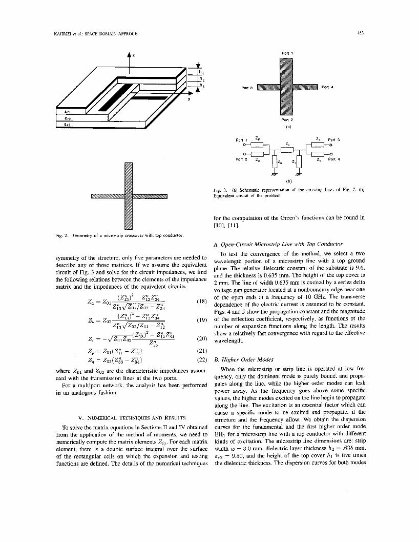
The crossover between two suspended striplines or two microstrip lines can be represented as a four-port network at some reference planes. Reference planes can be chosen at any position as long as they are on the continuous part of the transmission lines. Initially we find the scattering matrix from the field analysis utilizing the de-embedding procedure described in [4].
For the structure in Fig. 2 one may use the equivalent circuit representation shown in Fig. 3, [6]. The circuit satisfies the symmetry properties. In this representation, 2, and Zb are used to represent the two capacitances between the strips and the ground plane, while 2, represents the coupling capacitance between the two strips. Z, and 2, are used to describe the inductances associated with the two stripline sections. This is not a unique choice. However, based on this choice we compute the normalized impedance matrix [Z”] from the generalized scattering matrix [SI as
where [ I ] is the identity matrix. In general, the impedance matrix of a reciprocal four-port lossless network possesses ten independent imaginary parameters. However, because of the
KAHRIZI ef al.: SPACE DOMAIN APPROCH 453
Port 1
Port 1 zv
Port =q=p=o: 2 : M M
(b)
Fig. 3. Equivalent circuit of the problem.
(a) Schematic representation of the crossing lines of Fig. 2. (b)
for the computation of the Green's functions can be found in [lo], [111.
Fig. 2. Geometry of a microstrip crossover with top conductor.
A. Open-circuit Microstrip Line with Top Conductor
symmetry of the structure, only five parameters are needed to describe any of those matrices. If we assume the equivalent circuit of Fig. 3 and solve for the circuit impedances, we find the following relations between the elements of the impedance matrix and the impedances of the equivalent circuits
2, = ~ O l ( ~ , " , - Z,",) zq = 202(2;3 - 2,",)
(21) (22)
where 201 and 2 0 2 are the characteristic impedances associ- ated with the transmission lines at the two ports.
For a multiport network, the analysis has been performed in an analogous fashion.
v. NUMERICAL TECHNIQUES AND RESULTS
To solve the matrix equations in Sections I1 and IV obtained from the application of the method of moments, we need to numerically compute the matrix elements 2,. For each matrix element, there is a double surface integral over the surface of the rectangular cells on which the expansion and testing functions are defined. The details of the numerical techniques
To test the convergence of the method, we select a two wavelength portion of a microstrip line with a top ground plane. The relative dielectric constant of the substrate is 9.6, and the thickness is 0.635 mm. The height of the top cover is 2 mm. The line of width 0.635 mm is excited by a series delta voltage gap generator located at a nonboundary edge near one of the open ends at a frequency of 10 GHz. The transverse dependence of the electric current is assumed to be constant. Figs. 4 and 5 show the propagation constant and the magnitude of the reflection coefficient, respectively, as functions of the number of expansion functions along the length. The results show a relatively fast convergence with regard to the effective wavelength.
B. Higher Order Modes
When the microstrip or strip line is operated at low fre- quency, only the dominant mode is purely bound, and propa- gates along the line, while the higher order modes can leak power away. As the frequency goes above some specific values, the higher modes excited on the line begin to propagate along the line. The excitation is an essential factor which can cause a specific mode to be excited and propagate, if the structure and the frequency allow. We obtain the dispersion curves for the fundamental and the first higher order mode EH1 for a microstrip line with a top conductor with different kinds of excitation. The microstrip line dimensions are: strip width w = 3.0 mm, dielectric layer thickness hz = .635 mm, E,Z = 9.80, and the height of the top cover hl is five times the dielectric thickness. The dispersion curves for both modes

454 IEEE TRANSACTIONS ON MICROWAVE THEORY AND TECHNIQUES VOL. 42, NO. 3, MARCH 1994
.- c 0 0.4'
1 6
0 100 200 100 400 500
No. of expansion functions
Fig. 4. Propagation constant of a microstrip line with top conductor versus number of expansion functions. E , 1 = 1, c r z = 9.6. h , = 2.0 mm. h2 = 0.635 mm, 1~' = 0.635 mm.
0 $2.
' 'Or/---------I
0.90 I ,
0 100 m Mo too MO
No. of expansion functions
4 i 1
0 I , 0 IO 20 M 10 50
Frequency (GHz)
Fig. 6. order mode in a microstrip line with a top conductor. l ~ ~ l = 1, hl = 3 h 2 , 112 = 0.635 mm, u' = 3.0
Dispersion curves for the fundamental mode and the first higher = 9.8,
mm.
- present theory
Q Hill
+ Kirschning e t a(.
E2 E p: e
/ 4 e 12 16 24 20
Frequency (GHz)
Fig. 5. Reflection coefficient magnitude for an open-circuit microstrip line with top conductor versus number of expansion functions ~~1 = 1, cr2 = 9.6, hl = 2.0 mm, 112 = 0.635 mm, w = 0.635 mm.
Fig. 7. with c V l = 1, E , 2 = 9.8, hl = 2.515 mm, h a = 0.635 mm. u' = hi.
Magnitude of S parameters for a right-angle bend versus frequency
range between 6 and 20 GHz. Three subsections are used across the to allow for transverse current variation at high frequency. However, in the low frequency range below
GHz, the results are quite the Same when we use a constant transverse current distribution. The magnitude and the phase of S parameters are given in Figs. 7 and 8, respectively, and are compared with theoretical results of [12] in which the bend is located inside a square box of 12.7 mm side
are shown in Fig. 6. Similarly, we can excite the higher modes using proper excitation. The results agree with available results and this not only validates the analysis procedure but also the matrix pencil deembedding technique which has been used to generate the results.
C. Bend
As a two port network, we choose a symmetric right-angle bend in a two layer structure as shown in Fig. 8. The right- angle bend is formed by the junction of two transmission lines of 1.5X0 long. The bend is considered to be 0.635 mm wide and is situated on a grounded dielectric slab of E , . ~ = 9.8 and the thickness h2 of the dielectric is 0.635 mm. The entire structure is closed by a top conductor of the height hl = 2.545 mm. This example is analyzed in the frequency
length, and design formulas from [13], which were derived from measurements in the frequency range between 2 and 14 GHz for an open structure. The deviation in magnitude of 5'11 is negligible for the frequency range up to 16 GHz. However, larger differences are observed for the magnitude for frequencies beyond 16 GHz. Our results are located between the corresponding results of the open structure and those of the shielded one. The difference can be attributed to the effect

KAHRIZI et al.: SPACE DOMAIN APPROCH 455
- present theory a Hill
4 8 12 16 20 24
Frequency (GHz)
Fig. 8. Phase of S parameters for a right-angle bend versus frequency with = 1, ~~2 = 9.8, hl = 2.545 mm, hz = 0.635 mm, 10 = h l .
of the top conductor and the shielded box used in the analysis of [ 121. The phase is compared only with that for the shielded bend and the results are in good agreement Fig. 8. However, comparison of the phase with the bend in an open structure shows a large difference as is pointed out in [12].
D. T Junctions Next, we consider a basic T junction with three identical
finite transmission lines of 1.5X0 long as shown in Fig. 9. In the numerical procedure, the transverse dependence of the transmission lines is represented by three pulse functions. First, we consider an open microstrip T junction and then we compare the results for a T junction in the presence of top conductor. The structure has a dielectric layer of height hl = 0.635 mm and relative dielectric constant = 9.9. The width of the lines w is considered to be 0.609 mm. The results for the magnitudes of the scattering parameters as functions of frequency are compared with the results of the full-wave spectral analysis of [14] in Fig. 10. The results of [14] have been also verified by experimental work.
In Fig. 11, we consider the same case and that with a top ground plane of the height eight times the dielectric thickness. Good agreement is found below about 20 GHz, but the results begin to deviate as the frequency goes higher. This deviation is due to the effect of the top ground plane.
E. Crossover
The crossover structure and its equivalent circuit are il- lustrated in Figs. 2 and 3, respectively. This consists of two finite transmission lines of 3.0X0 long. The S parameters are calculated with hl = h3 = 5 mm, h2 = 1 mm, w1 = w 2 = 1 mm, E,I = ~ , 3 = 1, E,Z = 3.8, simulating the crossover model of the work in [6]. Since the structure is symmetric we can easily find the S parameters using only one excitation. However in order to show the precision of the method we have applied four different excitations, one at each port. The method of moments is then applied for each case, and the de- embedding procedure of Section IV yields a 16 by 16 matrix
Reterenw planes
..._ .....
H Port 3
Fig. 9. Schematic and cross section of a T junction
m P
sz L present theory WU
/
I -. I -15
0 5 10 15 20 25
Frequency (GHz)
Fig. 10. ~~2 = 9.9, h2 = 0.63.5 mm, ui = 0.609 mm.
Magnitude of S parameters of a microstrip T junction. E,I = 1,
to solve for the S parameters. From the S parameters, the impedance matrix and then the equivalent circuit elements are computed at the frequencies of 0.5, 1, and 2 GHz.
The element values L,, L,, c,, c b , and c, are defined as follows:

456 IEEE TRANSACTIONS ON MICROWAVE THEORY AND TECHNIQUES VOL. 42, NO. 3, MARCH 1994
Fig. 11. E ~ Z = 9.9, hz = 0.635 mm, w = 0.609 mm.
Magnitude of S parameters of a microwave T junction. ~~1 = 1,
TABLE I ELEMENT VALUES OF EQUIVALENT CIRCUIT BY THIS ~ A L Y S I S
.5 GHz 1 GHz 2 GHz L, = L, 0.339 nH 0.338 nH 0.319 nH
C C 0.421 pF 0.283 pF 0.231 pF c a = cb -0.1 15 pF -0.100 pF -0.096 pF
TABLES I1 ELEMENT VALUES OF EQUIVALENT Cmcurr BY Uwano et al.
.5 GHz 1 GHz 2 GHz L, = L , 0.331 nH 0.331 nH 0.329 nH . - c, = Cb -0.0885 pF -0.103 pF -0,101 pF CC 0.249 pF 0.272 pF 0.258 pF
Tables I and I1 show the results computed by this method and by that of [6]. At the frequencies 1 and 2 GHz, the results agree well. However, in [6] it is assumed that there are side walls. The magnitudes of S parameters for the frequency range from .5 GHz to 10 GHz are shown in Fig. 12. Since the structure is symmetric, only three independent parameters are sufficient to determine the scattering matrix.
VI. CONCLUSION
In this paper, a numerical approach has been described to analyze printed circuits of various kinds. The method is based on the space domain integral equation. Method of moments has been used to solve the coupled integral equations for the electric surface currents existing on different parts of the structures. Matrix pencil technique has been applied for the analysis of the current distribution in order to evaluate the circuit parameters. This makes it possible to find the S- parameters at reference planes quite close to the discontinuity and without considering large transmission lines feeding the structures.
The validity of this approach has been discussed extensively, and it has been found that it can be used to describe other problems in printed circuits. For example, the problems with loss are among those kinds of problems which can easily be
0 0 0 1 1 2 3 1 5 6 7 8 9 10 I1
Frequency (GHz)
Fig. 12. Magnitudes of S parameters of a crossover as functions of fre- quency. E ~ I = ~~3 = 1.0, cr2 = 3.8, hl = 123 = 5 mm, hz = 1.0 mm, tu1 = u12 = 1.0 mm.
analyzed utilizing this approach. The main advantage of this approach is the ease with which even the most complicated structures can be evaluated. A number of practical structures have been studied and their most interesting features discussed.
RFFERENCES
[I] N. K. Das and D. M. Pozar, “A generalized spectral-domain Green’s function for multilayer dielectric substrates with application to multi- layer transmission lines,” IEEE Trans. Microwave Theory Tech., vol. MTT-35, pp. 32G33.5, Mar. 1987.
[2] R. H. Jansen and N. H. L. Koster, “New aspects concerning the definition of microstrip characteristic impedance as a function of frequency,” in IEEE I982 Int. Microwave Symp. Dig., Dallas, TX, pp. 305-307.
[3] J. R. Brews, “Characteristic impedance of microstrip line,”IEEE Trans. Micmwave Theory Tech., vol. M’IT-35, pp. 30-34, Jan. 1987.
[4] T. K. Sarkar, 2. A. MariCeviC, and M. Kahrizi, “An accurate deembed- ding procedure for characterizing discontinuities,”Int. J. MIMICAE, vol. 2, no. 3, pp. 135-143, 1992.
[5] Y. Kami and R. Sato, “Coupling model of crossing transmission lines,” IEEE Trans. Electromagn. Compat., vol. EMC-28, pp. 20&210, Nov. 1986.
[6] T. Uwano, R. Sorrentino, and T. Itoh, “Characterization of strip line crossing by transverse resonance analysis,” IEEE Trans. Microwave Theory Tech., vol. MTT-35. pp. 1369-1376, Dec. 1987.
[7] S. Papatheodorou, R. F. Hanington, and J. R. Mautz, “The equivalent circuit of a microstrip crossover in a dielectric substrate,” IEEE Trans. Microwave Theory Tech., vol. 38, pp. 135-140, Feb. 1990.
[8] S. Papatheodorou, J. R. Mautz, and R. F. Harrington, “Full-wave analysis of a strip crossover,” IEEE Trans. Microwave Theory Tech., vol. 38, pp. 1439-1447, Oct. 1990.
[9] H. Y. Yang and N. G. Alexopoulos, “Basic blocks for high-frequency interconnects: Theory and experiment,” IEEE Trans. Micmwave Theory Tech., vol. 36, pp. 1258-1264, Aug. 1988.
[IO] J. R. Mosig and T. K. Sarkar, “Comparison of quasi-static and exact electromagnetic fields from a horizontal electric dipole above a lossy di- electric backed by an imperfect ground plane,” IEEE Trans. Microwave Theory Tech., vol. MTT-34, pp. 379-387, Apr. 1986.
I I] T. Itoh, Numerical Techniques for Microwavc. and Millimeter-Wave Passive Structures. Wiley, 1989.
121 A. Hill and V. K. Tripathi, “An efficient algorithm for the three- dimensional analysis of passive microstrip component and disconti- nuities for microwave and millimeter-wave integrated circuits,”ZEEE Trans. Microwave Theory Techn., Vol. 39, pp, 83-91, Jan. 1991.
131 M. Kirschning, R. H. Jansen, and N. H. L. Koster, “Measurement and computer-aided modeling of microstrip discontinuities by an improved resonator method,” IEEE M U - S In?. Microwavc. Symp. Dig., 1983, pp. 495-497.

KAHRIZI er al.: SPACE DOMAIN APPROCH 451
S.-C. Wu, H.-Y. Yang, N. G. Alexopoulos, and I. Wolff, “A rigorous dispersive characterization of microstrip cross and T junctions,” IEEE Trans. Microwave Theory Tech., vol. 38, pp. 1837-1844, Dec. 1990. T. Becks and I. Wolff, “Full-wave analysis of 3D metallization structures using a spectral domain technique,” M7T-S Int. Microwave Symp. Dig., 1992, pp. 1123-1 126.
Tapan Kumar Sarkar (S’69-M’76-SM’81-F’92), for a photograph and biography, see page 250 of the February issue of this TRANSACTIONS.
Z. Ma&evit, T. Sarkar, Y. Hua, and A. R. Djordjevit, “Time domain measurements with the Hewlett Packard Network Analyzer HP8510 using the matrix pencil method,” IEEE Trans. Microwave Theory Tech., vol. 39, pp. 538-547, Mar. 1991, .
Masoud Kahrizi was born in Arak, Iran, in 1960. He received the B.S. degree from Esfahan Univer- sity of Technology, Esfahan, Iran, the M.Sc. degree from the University of Tehran, Tehran, Iran, and the Ph.D. degree from Syracuse University, Syracuse, NY, all in electrical engineering, in 1986, 1988, and 1992, respectively.
He is currently an Assistant Professor in the De- partment of Electrical Engineering at Tarbiat Modar- res University, Tehran. Iran. His research interests
Zoran A. MariCeviC (M’89-S’90) was born August 21, 1961 in Arandjelovac, Yugoslavia. He received the Diploma Engineer degree from the University of Belgrade in 1986 and the M.S. in electrical engineering from Syracuse University, Syracuse, NY in 1992..
From 1988 to 1992, he was the Microwave Lab- oratory Manager in the Department of Electrical and Computer Engineering at Syracuse University. He served as an Adjunct Instructor in MIcrowave Measurement at the same university in 1992. His
research interests are in microwave measurements, numerical electromagnet- ics, bio-effects of electromagnetic fields and applied mathematics.
He is a member of the American Geophysical Union.
include numerical problems in electromagnetics and characterization of radiating discontinuities.