solid state detectors lecture for summer students at · pdf filesteinbrück: solid state...
TRANSCRIPT
Solid State Detectors
Lecture for Summer Students at DESY
Georg Steinbrück
Hamburg UniversityAugust 15, 2008
Steinbrück: Solid State Detectors 2
Content
• Interaction of Particles with Matter
• Solid State Detectors: Motivation and Introduction
• Materials and their Properties
• Energy Bands and Electronic Structure
• The pn-Junction
• Charge Collection: Diffusion and Drift
• Energy Resolution
• Limitations of Silicon Detectors: Radiation Damage
• Detector Types + Production of Silicon Detectors
• Readout and Noise
• Momentum Measurements and Track Finding
• Summary
Interaction of Particles with Matter

Steinbrück: Solid State Detectors 4
Interaction of Particles with Matter
For charged particles:
• Inelastic collisions with electrons of the atomic shell
• Soft (Atoms are only excited)
• Hard: (Atoms become ionized)
δ-Rays (Energy of knocked-out electrons big enough to ionize further atoms).
• Elastic collisions with nuclei
• Cherenkov-Radiation
• Bremsstrahlung
• Deceleration of charged particles with E>>m over small distance: Electrons
• Nuclear reactions
Bethe-Bloch Formula(see following page)

m: rest mass of the electron
β: =v/c rel. velocity of particle.
γ:γ:γ:γ: =(1-ββββ2)-1/2 Lorentz-Factor
ze: electric charge of incident particle
Z: atomic number of medium
n: number of atoms per unit vol.
=ρρρρA0/A; A0: Avogadro-number A:
atomic mass, ρ: ρ: ρ: ρ: spec. density of medium
δ: δ: δ: δ: density parameter
I: mean ionization potential
Interaction of Particles with Matter
−−
=−
2
2ln
)4(
4 2222
222
0
42 δβγ
β
βπε
π
I
cm
cm
nZez
dx
dE Bethe-Bloch Formula
for heavy particles
Relativistic rise ~ln
~1/v2
Non-
relativistic
MIP
ionisation and excitation
-
gas
Solid media
describes Energy loss per distance traveled,
„stopping power“
Density effect

Interaction of Particles with Matter
Note units: Here in MeV per path length and density to be more comparable accross materials.
To get to MeV/cm multiply with density ρ.
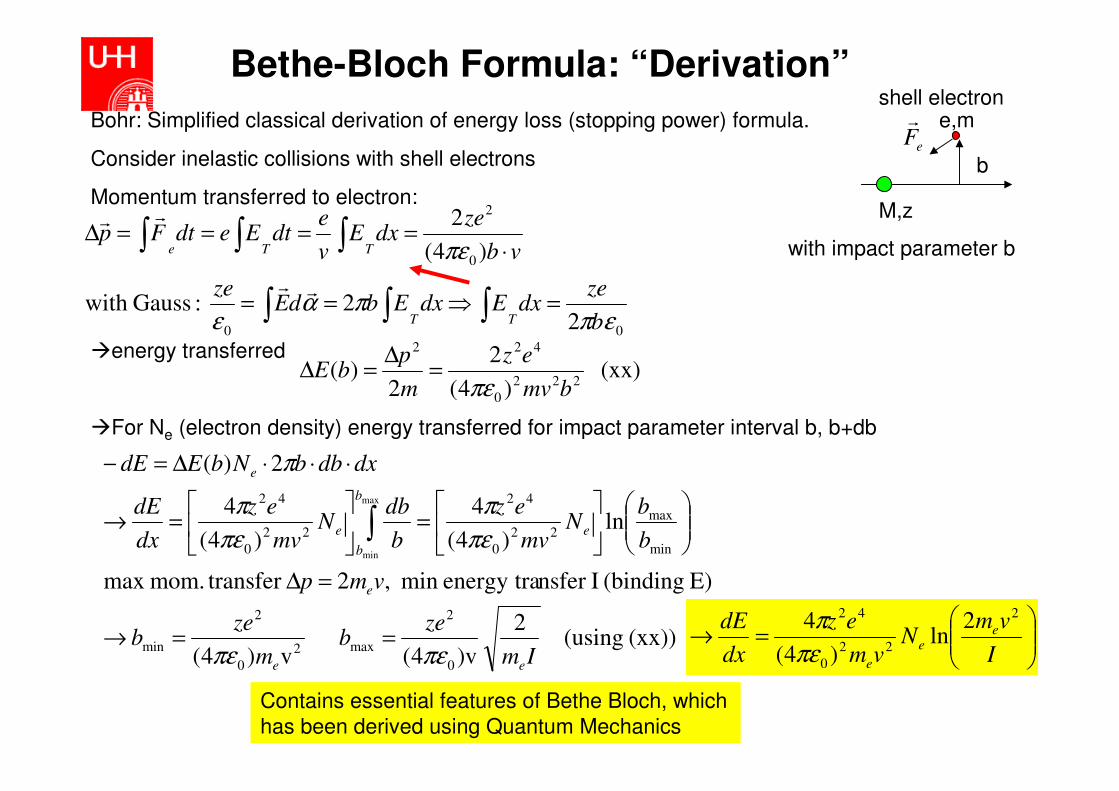
Bethe-Bloch Formula: “Derivation”
Bohr: Simplified classical derivation of energy loss (stopping power) formula.
Consider inelastic collisions with shell electrons
Momentum transferred to electron:
energy transferred
For Ne (electron density) energy transferred for impact parameter interval b, b+db
b
e,m
M,z
00
0
2
22 :Gausswith
)4(
2
εππα
ε
πε
b
zedxEdxEbdE
ze
vb
zedxE
v
edtEedtFp
TT
TTe
=⇒==
⋅====∆
∫∫∫
∫∫∫rr
rr
eFr
(xx) )4(
2
2)(
222
0
422
bmv
ez
m
pbE
πε=
∆=∆
(xx)) (using 2
)v4(
v)4(
E) (binding Insfer energy tramin ,2 transfer mom.max
ln)4(
4
)4(
4
2)(
0
2
max2
0
2
min
min
max
22
0
42
22
0
42 max
min
Im
zeb
m
zeb
vmp
b
bN
mv
ez
b
dbN
mv
ez
dx
dE
dxdbbNbEdE
ee
e
e
b
b
e
e
πεπε
πε
π
πε
π
π
==→
=∆
=
=→
⋅⋅⋅∆=−
∫
=→
I
vmN
vm
ez
dx
dE ee
e
2
22
0
42 2ln
)4(
4
πε
π
Contains essential features of Bethe Bloch, which
has been derived using Quantum Mechanics
with impact parameter b
shell electron
Steinbrück: Solid State Detectors 8
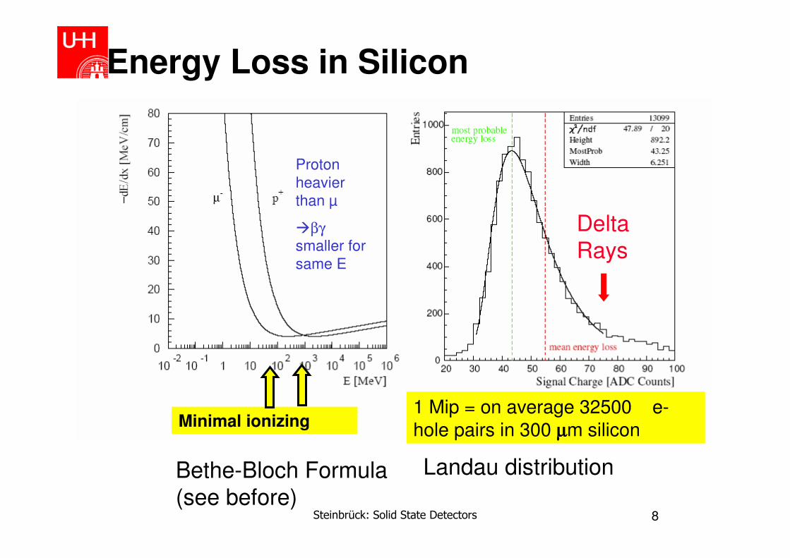
Energy Loss in Silicon
Minimal ionizing
Delta Rays
1 Mip = on average 32500 e-
hole pairs in 300 µµµµm silicon
Landau distributionBethe-Bloch Formula(see before)
Proton
heavier
than µ
βγsmaller for
same E
Steinbrück: Solid State Detectors 9
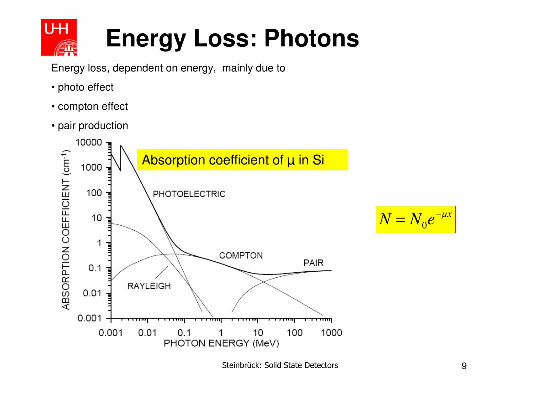
Energy Loss: Photons
Minimal ionizing
Absorption coefficient of µ in Si
Energy loss, dependent on energy, mainly due to
• photo effect
• compton effect
• pair production
µxeNN
−= 0

Solid State Detectors:Motivation and Introduction

Steinbrück: Solid State Detectors 11
Solid State Detectors: Motivation Semiconductors have been used in particle identification for many years.
• ~1950: Discovery that pn-Junctions can be used to detect particles.
Semiconductor detectors used for energy measurements (Germanium)
• Since ~ 25 years: Semiconductor detectors for precise position measurements.
• Of special Interest: Discovery of short lived b-and c-mesons, τ-leptons
• life times (0.3-2)x10-12 scττττ=100-600µm
• precise position measurements possible through fine segmentation (10-100µm)
multiplicities can be kept small (goal:<1%)
• Technological advancements in production technology:
• developments for micro electronics (lithographic chip processing)
• Electrons and holes move almost freely in silicon:
Fast Readout possible (O(20 ns)): LHC: 25 ns “bunch spacing”
• Generation of 10x more charge carriers compared to typical gases (for the same energy loss)
• Radiation hardness
Steinbrück: Solid State Detectors 12
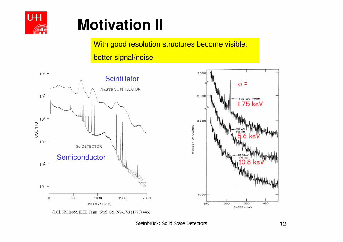
Motivation IIWith good resolution structures become visible,
better signal/noise
Scintillator
Semiconductor
Steinbrück: Solid State Detectors 13
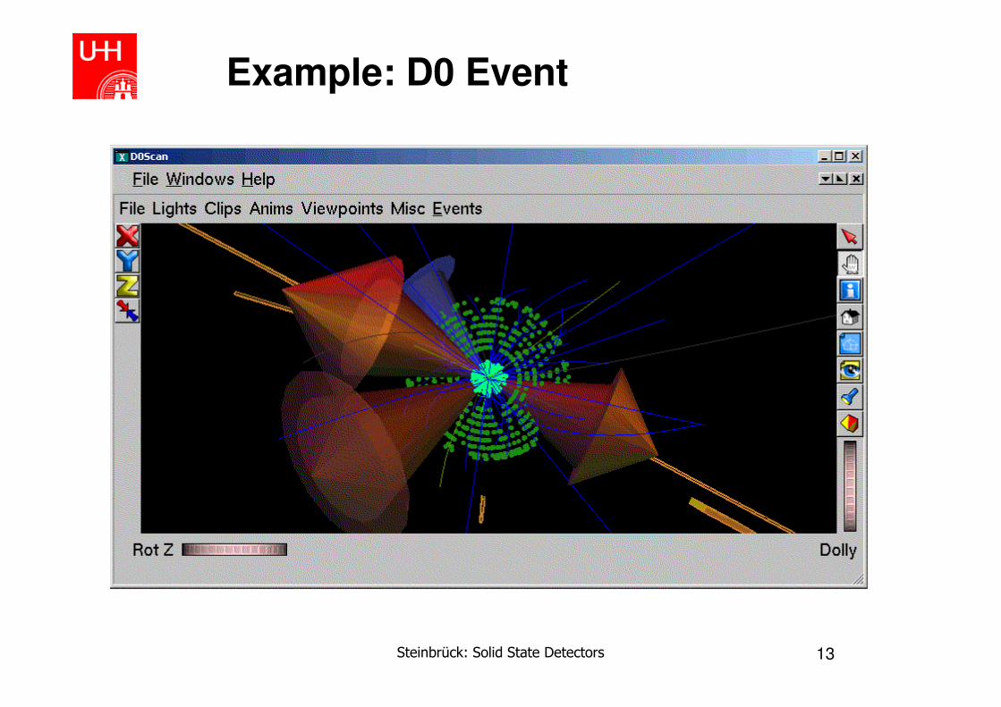
Example: D0 Event

Steinbrück: Solid State Detectors 14
Example: CMS Event (simulated): ttHbb

Steinbrück: Solid State Detectors 15
Example: CMS Event (simulated): ttHbb zoomed in
Steinbrück: Solid State Detectors 16
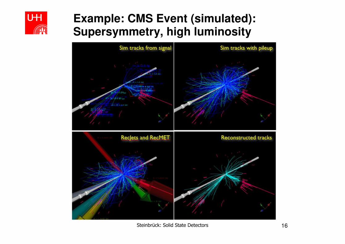
Example: CMS Event (simulated): Supersymmetry, high luminosity
Steinbrück: Solid State Detectors 17
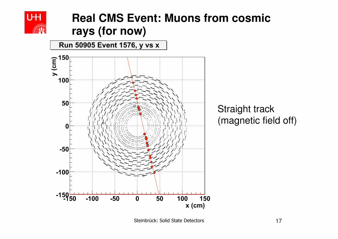
Real CMS Event: Muons from cosmic rays (for now)
Straight track(magnetic field off)

Steinbrück: Solid State Detectors 18
A. Castoldi et al, NIM-A518(2004)426
Thaumatin electron density map(natürlich vorkommender Süßstoff)
106 pixels of~0.2x0.2 mm2
C.Brönnimann et al., J.Synchr.Rad. 13(2006)120
Example: Hybrid Pixel Detector Pilatus (PSI-CH) for X-ray crystallography

Steinbrück: Solid State Detectors 19
Solid State Detectors: General Remarks
Generally, Two kids of solid state detectors can be distinguished:
• Photo resistors: Resistance changes with irradiation
• Photo diode: Depleted semiconductor layer with typically large electric field used as active zone
ionization chamber

Steinbrück: Solid State Detectors 20
Working Principles
Detection volume with electric field
Charge carrier pairs generated via ionization
Charges drift in the electric field
external electric signal
Velocity of charge carriers, v
Rate of induced charges on
electrode
Signal charge, often Q~E
Peak voltage ~Q~E

Materials and their properties
Steinbrück: Solid State Detectors 22
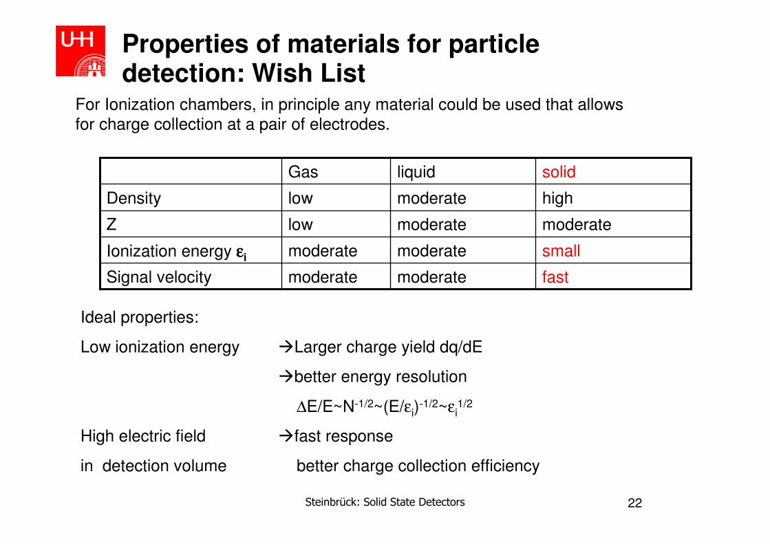
Properties of materials for particle detection: Wish List
For Ionization chambers, in principle any material could be used that allows for charge collection at a pair of electrodes.
fastmoderatemoderateSignal velocity
smallmoderatemoderateIonization energy εεεεi
moderatemoderatelowZ
highmoderatelowDensity
solidliquidGas
Ideal properties:
Low ionization energy Larger charge yield dq/dE
better energy resolution
∆E/E~N-1/2~(E/εi)-1/2~εi
1/2
High electric field fast response
in detection volume better charge collection efficiency
Steinbrück: Solid State Detectors 23
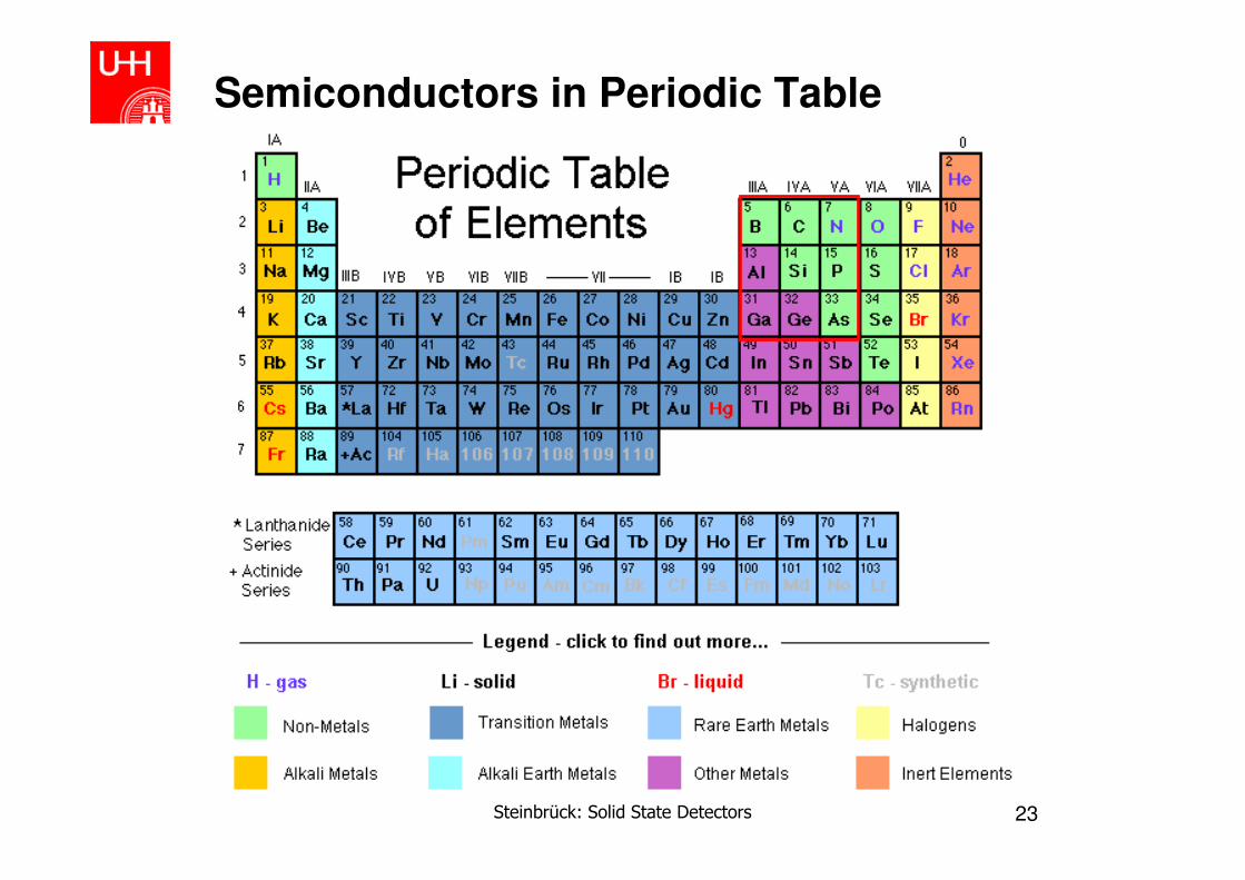
Semiconductors in Periodic Table

Energy bands and electronic structure
Steinbrück: Solid State Detectors 25
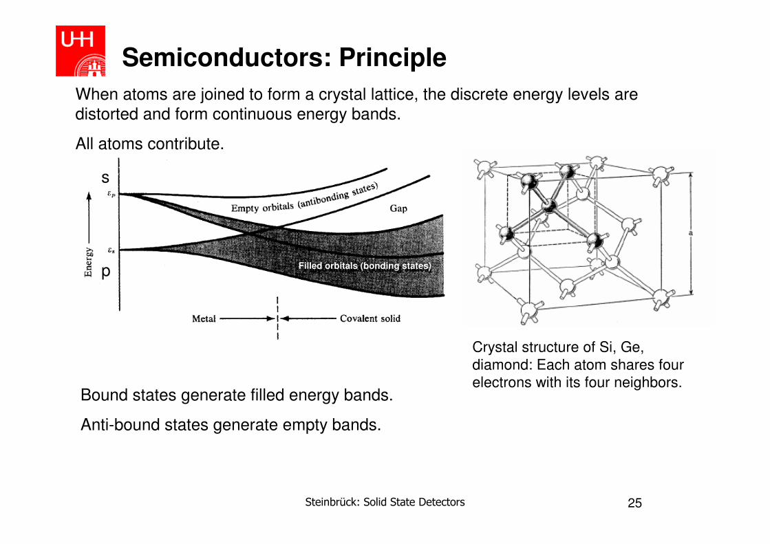
Semiconductors: Principle
When atoms are joined to form a crystal lattice, the discrete energy levels are distorted and form continuous energy bands.
All atoms contribute.
Bound states generate filled energy bands.
Anti-bound states generate empty bands.
Crystal structure of Si, Ge,
diamond: Each atom shares four
electrons with its four neighbors.
Filled orbitals (bonding states)
s
p
Steinbrück: Solid State Detectors 26
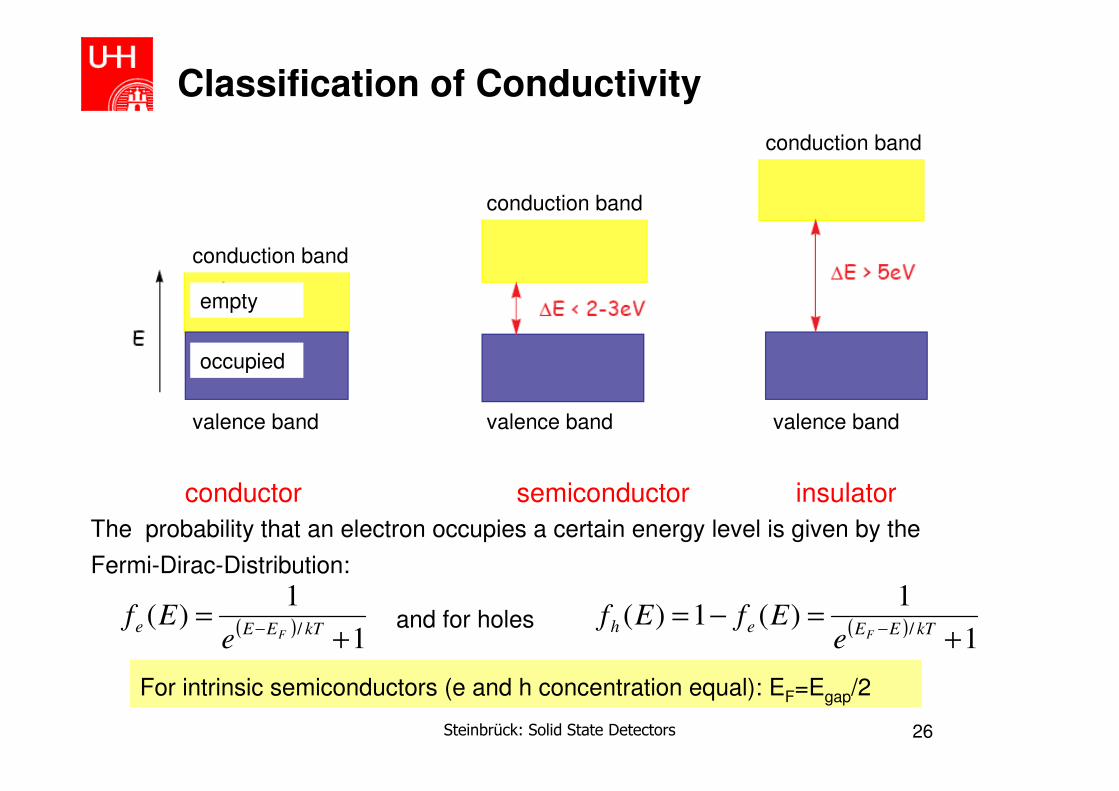
Classification of Conductivity
( )1
1)(
/ +=
− kTEEeFe
Ef
The probability that an electron occupies a certain energy level is given by the
Fermi-Dirac-Distribution:
( )1
1)(1)(
/ +=−=
− kTEEehFe
EfEfand for holes
For intrinsic semiconductors (e and h concentration equal): EF=Egap/2
conductor
conduction band
conduction band
conduction band
valence band valence bandvalence band
empty
occupied
semiconductor insulator
Steinbrück: Solid State Detectors 27
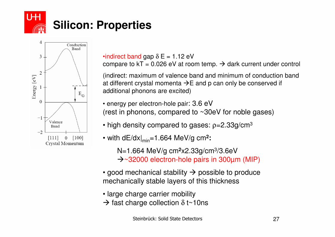
Silicon: Properties
•indirect band gap δ E = 1.12 eVcompare to kT = 0.026 eV at room temp. dark current under control
(indirect: maximum of valence band and minimum of conduction band
at different crystal momenta E and p can only be conserved if
additional phonons are excited)
• energy per electron-hole pair: 3.6 eV(rest in phonons, compared to ~30eV for noble gases)
• high density compared to gases: ρ=2.33g/cm3
• with dE/dx|min=1.664 MeV/g cm2:
N=1.664 MeV/g cm2x2.33g/cm3/3.6eV
~32000 electron-hole pairs in 300µm (MIP)
• good mechanical stability possible to produce
mechanically stable layers of this thickness
• large charge carrier mobility
fast charge collection δ t~10ns

Steinbrück: Solid State Detectors 28
Semiconductors: General Properties
Ratio Eion/EGap independant of
• material
• type of radiation
Reason: Fraction of energy going into
phonons (momentum transfer) is
approximately the same for all
semiconductors.

Steinbrück: Solid State Detectors 29
Semiconductors Compared
Si
• currently best compromise for strip
detectors
Ge
• small band gaphigh amount of charge
produced good for energy measurements
• high intrinsic charge carrier concentration
has to be cooled (liquid N2)
GaAs
• good ratio generated charge/ noise
• but: charge collection efficiency strongly
dependent on purity and composition
• radiation hard
Diamond
• radiation hard, but still quite expensive
• charge collection length ~ 80µm
Property
Z
A
Band gap
radiation length X0
mean energy to generate eh pair
mean E-loss dE/dx
mean signal produced
intrinsic charge carrier concentration ni
electron mobility
hole mobility
Steinbrück: Solid State Detectors 30
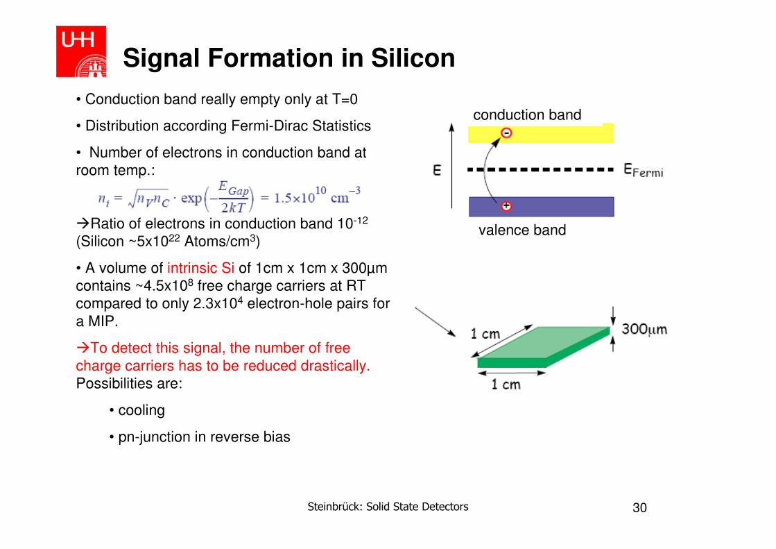
Signal Formation in Silicon
• Conduction band really empty only at T=0
• Distribution according Fermi-Dirac Statistics
• Number of electrons in conduction band at
room temp.:
Ratio of electrons in conduction band 10-12
(Silicon ~5x10²² Atoms/cm3)
• A volume of intrinsic Si of 1cm x 1cm x 300µm
contains ~4.5x10⁸ free charge carriers at RT
compared to only 2.3x10⁴ electron-hole pairs for
a MIP.
To detect this signal, the number of free
charge carriers has to be reduced drastically.
Possibilities are:
• cooling
• pn-junction in reverse bias
conduction band
valence band

Steinbrück: Solid State Detectors 31
Interlude: Doping
• Pure silicon has a very high resistance at room temp. (235 kOhm cm)
• Doping: A few silicon atoms can be replaced by atoms of an element of the 3rd main group (i.e. Boron) p type, or of the 5th main group (i.e.
Phosphorus) n type.
Important: Charge carriers only weakly bound.
Typical doping concentration 10-11 !
n type: Fermi level in upper half
p type: in lower half

The pn junction

Steinbrück: Solid State Detectors 33
The pn junction
External voltage in the same direction as generated potential (Diode in reverse bias)
Increase of depletion region (Layer depleted of free charge carriers)
Outstandingly useful for the detection of ionizing radiation.
- +
Vbias
electrons drift towards p-side, holes towards n-side buildup of a potential.
neg. space
chargepos. space
charge
Steinbrück: Solid State Detectors 34
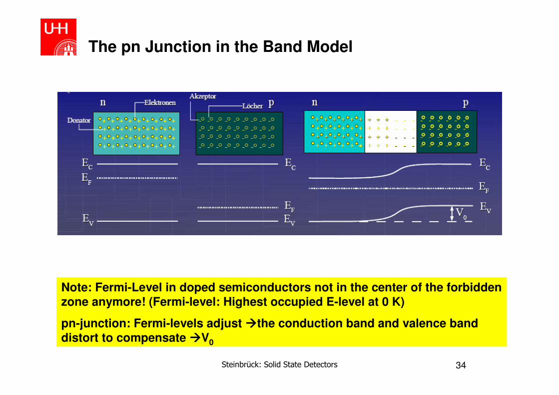
The pn Junction in the Band Model
Note: Fermi-Level in doped semiconductors not in the center of the forbidden
zone anymore! (Fermi-level: Highest occupied E-level at 0 K)
pn-junction: Fermi-levels adjust the conduction band and valence band
distort to compensate V0
Steinbrück: Solid State Detectors 35
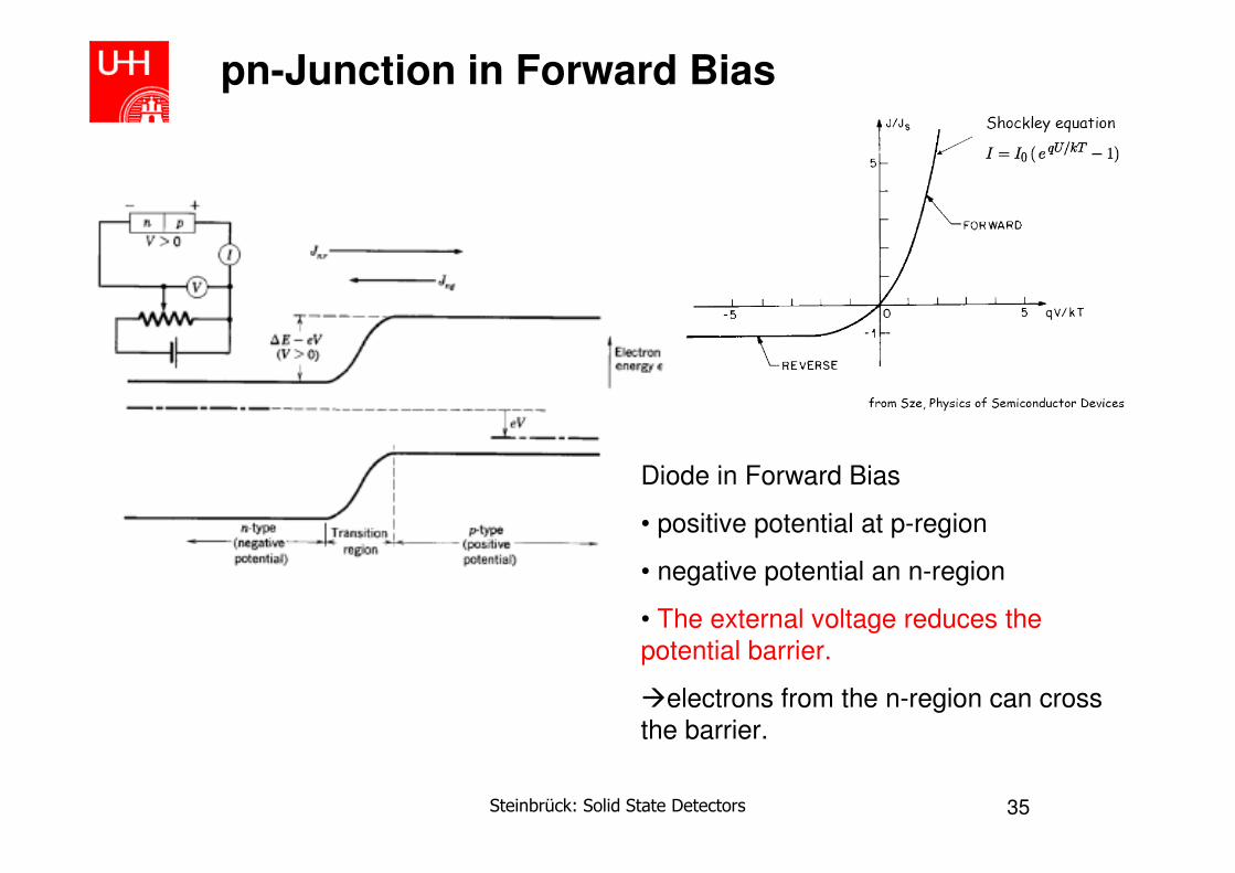
pn-Junction in Forward Bias
Diode in Forward Bias
• positive potential at p-region
• negative potential an n-region
• The external voltage reduces the potential barrier.
electrons from the n-region can cross the barrier.

Steinbrück: Solid State Detectors 36
pn Junction in Reverse Bias
• The external voltage increases the potential barrier
• The depletion zone can be used as detector, since it contains an electric field (and is depleted of free
charges).
Break through:
Detector behaves like a
conductor (charge avalanche)
Leakage current: Thermal generation of
e h pairs temperature dependant
V∝
Steinbrück: Solid State Detectors 37
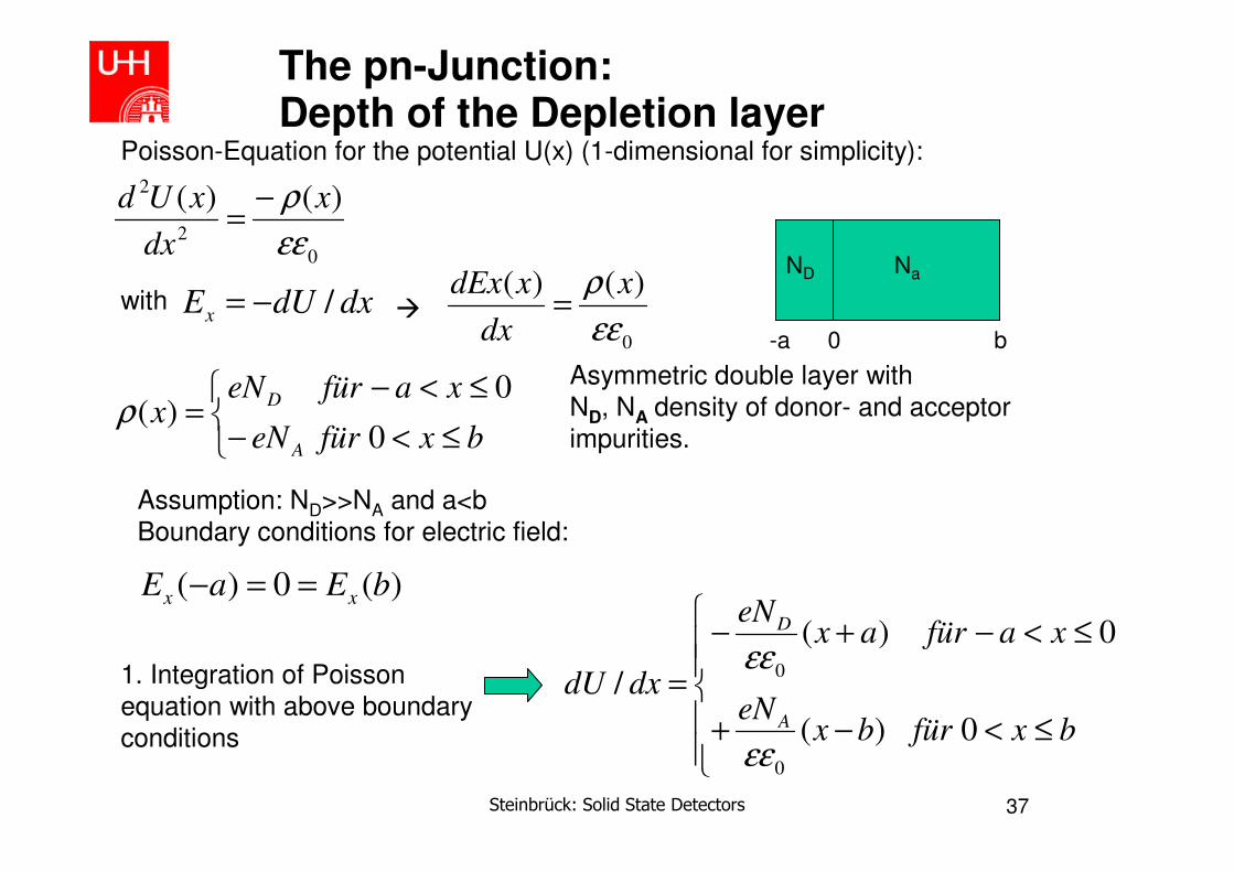
The pn-Junction:Depth of the Depletion layer
0
2
2 )()(
εε
ρ x
dx
xUd −=
Poisson-Equation for the potential U(x) (1-dimensional for simplicity):
dxdUEx /−=with
0
)()(
εε
ρ x
dx
xdEx=
≤<−
≤<−=
bxfüreN
xafüreNx
A
D
0
0)(ρ
Asymmetric double layer withND, NA density of donor- and acceptor impurities.
Assumption: ND>>NA and a<bBoundary conditions for electric field:
)(0)( bEaE xx ==−
≤<−+
≤<−+−
=
bxfürbxeN
xafüraxeN
dxdUA
D
0)(
0)(
/
0
0
εε
εε1. Integration of Poisson equation with above boundary conditions
0 b-a
NaND

Steinbrück: Solid State Detectors 38
Depth of the Depletion Layer II
Boundary condition for the potential:
≤<−−+
≤<−+−
=
bxfürUbxeN
xafüraxeN
xUA
D
0)(2
0)(2
)(
0
2
0
2
0
εε
εε
2. Integration:
0)(0)( UbUundaU −==−
Use NDa= NAb and continuity at x=0:
AeN
Ubab 002
)(εε
=+
applied voltage
For the strongly asymmetric case (ND>>NA) b>>a (b: thickness of p-doped layer)
d=a+b~b
AeN
Ud 002εε
=
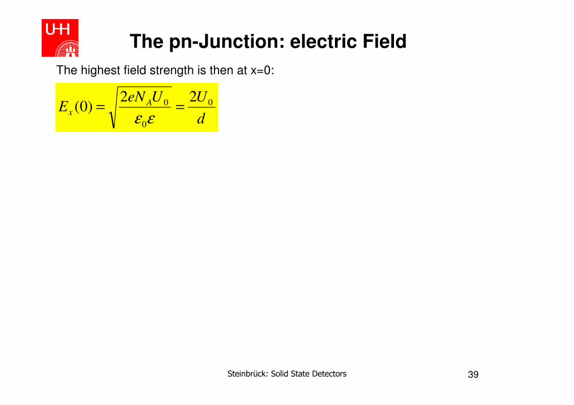
Steinbrück: Solid State Detectors 39
The pn-Junction: electric Field
The highest field strength is then at x=0:
d
UUeNE A
x0
0
0 22)0( ==
εε

Steinbrück: Solid State Detectors 40
Der pn junction: Overview
No free charge carriers
Asymmetry due to
different levels of
doping
Depletion zone
Diffusion of e in p zone
Diffusion of holes in n
zone

Charge collection : Diffusion and Drift
Steinbrück: Solid State Detectors 42
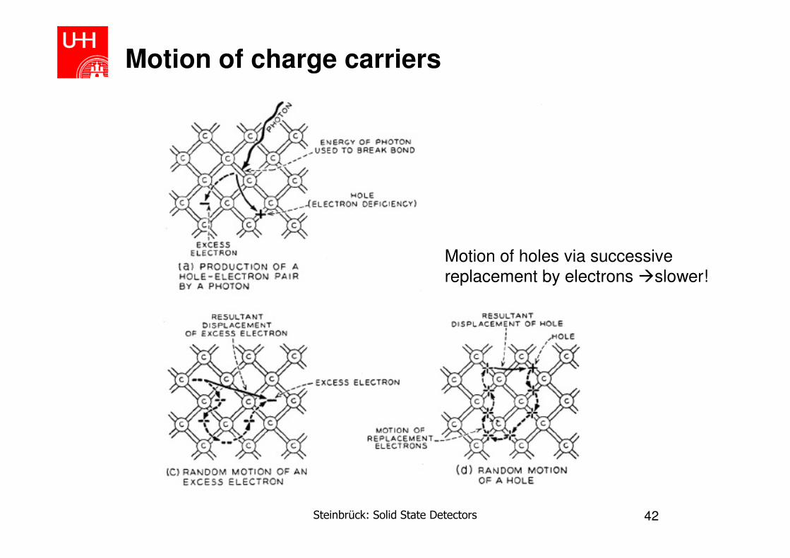
Motion of charge carriers
Motion of holes via successive replacement by electrons slower!
Steinbrück: Solid State Detectors 43
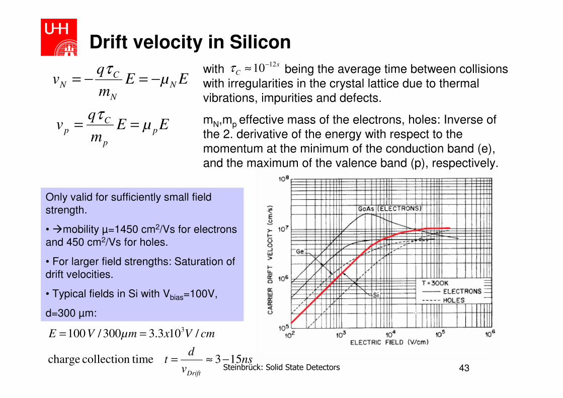
Drift velocity in Silicon
Only valid for sufficiently small field
strength.
• mobility µ=1450 cm2/Vs for electrons
and 450 cm2/Vs for holes.
• For larger field strengths: Saturation of
drift velocities.
• Typical fields in Si with Vbias=100V,
d=300 µm:
with being the average time between collisions with irregularities in the crystal lattice due to thermal vibrations, impurities and defects.
mN,mp effective mass of the electrons, holes: Inverse of the 2. derivative of the energy with respect to the momentum at the minimum of the conduction band (e), and the maximum of the valence band (p), respectively.
EµEm
qv N
N
CN −=−=
τ s
C
1210−≈τ
EµEm
qv p
p
Cp ==
τ
nsv
dt
cmVxµmVE
Drift
153 timecollection charge
/103.3300/100 3
−≈=
==
Steinbrück: Solid State Detectors 44
Diffusion
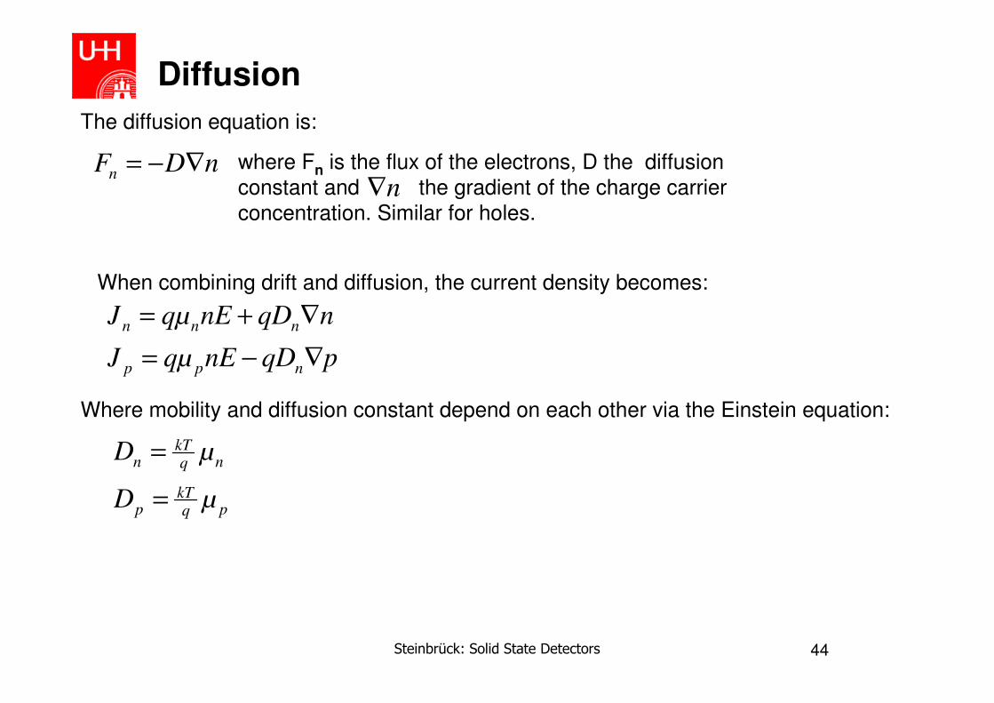
nDFn ∇−= where Fn is the flux of the electrons, D the diffusion constant and the gradient of the charge carrier concentration. Similar for holes.
n∇
The diffusion equation is:
When combining drift and diffusion, the current density becomes:
pqDnEqµJ
nqDnEqµJ
npp
nnn
∇−=
∇+=
Where mobility and diffusion constant depend on each other via the Einstein equation:
pqkT
p
nqkT
n
µD
µD
=
=

Energy Resolution
Steinbrück: Solid State Detectors 46
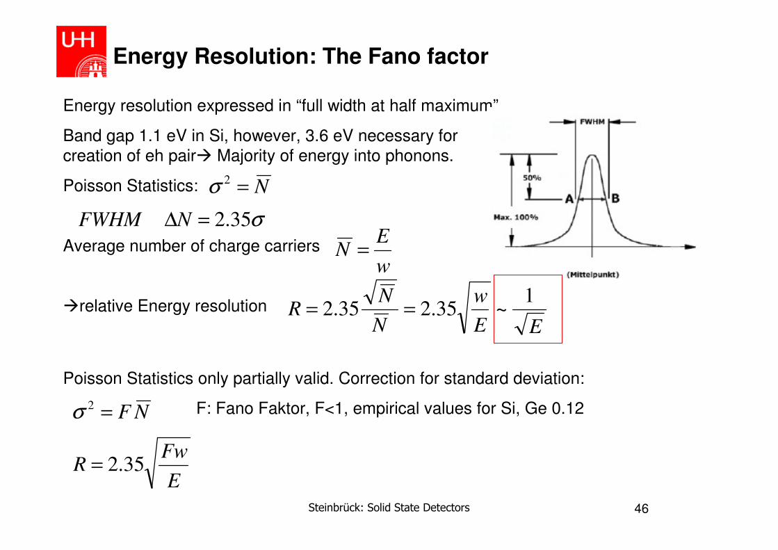
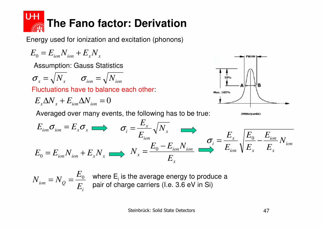
Energy Resolution: The Fano factor
Energy resolution expressed in “full width at half maximum”
Band gap 1.1 eV in Si, however, 3.6 eV necessary for creation of eh pair Majority of energy into phonons.
Poisson Statistics:
Average number of charge carriers
relative Energy resolution
N=2σ
σ35.2=∆NFWHM
w
EN =
EE
w
N
NR
1~35.235.2 ==
NF=2σ
Poisson Statistics only partially valid. Correction for standard deviation:
F: Fano Faktor, F<1, empirical values for Si, Ge 0.12
E
FwR 35.2=
Steinbrück: Solid State Detectors 47
The Fano factor: Derivation
xx N=σ
0=∆+∆ ionionxx NENE
xxionion EE σσ =
xxionion NENEE +=0
Energy used for ionization and excitation (phonons)
Assumption: Gauss Statistics
ionion N=σFluctuations have to balance each other:
Averaged over many events, the following has to be true:
x
ion
xi N
E
E=σ
xxionion NENEE +=0x
ionionx
E
NEEN
−= 0
ion
x
ion
xion
xi N
E
E
E
E
E
E−= 0σ
i
QionE
ENN 0== where Ei is the average energy to produce a
pair of charge carriers (I.e. 3.6 eV in Si)

Steinbrück: Solid State Detectors 48
Derivation II
The variance in the ionization process is
ix
ion
xion
xion
E
E
E
E
E
E
E
E 00 −=σ
−⋅= 10
ion
i
ion
x
i
ionE
E
E
E
E
Eσ
Which can be written as:
Fano Factor F
i
QE
EN 0=Since
and proportional to the variance of the signal charge Q: ionσ
QQ FN=σ
For silicon:
)1.0:(
08.06.3
,1.1,037.0
≈
=→=
===
measured
FeVE
eVEEeVE
i
gionx

Limitations of Silicon Detectors: Radiation Damage
Steinbrück: Solid State Detectors 50
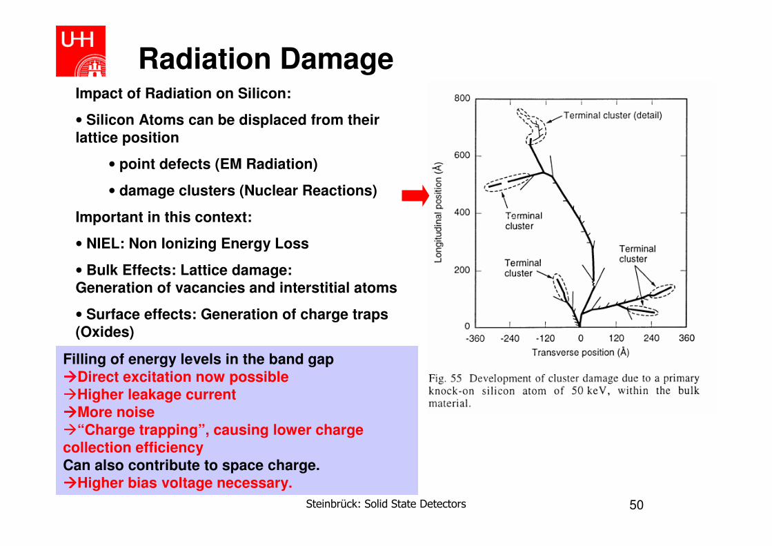
Impact of Radiation on Silicon:
• Silicon Atoms can be displaced from their
lattice position
• point defects (EM Radiation)
• damage clusters (Nuclear Reactions)
Important in this context:
• NIEL: Non Ionizing Energy Loss
• Bulk Effects: Lattice damage:
Generation of vacancies and interstitial atoms
• Surface effects: Generation of charge traps
(Oxides)
Filling of energy levels in the band gap
Direct excitation now possible
Higher leakage current
More noise
“Charge trapping”, causing lower charge
collection efficiency
Can also contribute to space charge.
Higher bias voltage necessary.
Radiation Damage

Steinbrück: Solid State Detectors 51
Radiation Exposure at CMS
Unit: Neutrons per cm2
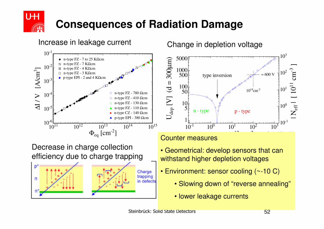
Steinbrück: Solid State Detectors 52
10-1 100 101 102 103
Φeq [ 1012 cm-2 ]
1
510
50100
5001000
5000
Ud
ep [
V]
(d =
300µ
m)
10-1
100
101
102
103
| Neff |
[ 1
01
1 c
m-3
]
≈ 600 V≈ 600 V
1014cm-21014cm-2
p - typep - type
type inversiontype inversion
n - typen - type
[Data from R. Wunstorf 92]
Consequences of Radiation Damage
Increase in leakage current Change in depletion voltage
1011 1012 1013 1014 1015
Φeq [cm-2]
10-6
10-5
10-4
10-3
10-2
10-1
∆I
/ V
[
A/c
m3]
n-type FZ - 7 to 25 KΩcmn-type FZ - 7 to 25 KΩcm
n-type FZ - 7 KΩcmn-type FZ - 7 KΩcm
n-type FZ - 4 KΩcmn-type FZ - 4 KΩcm
n-type FZ - 3 KΩcmn-type FZ - 3 KΩcm
n-type FZ - 780 Ωcmn-type FZ - 780 Ωcm
n-type FZ - 410 Ωcmn-type FZ - 410 Ωcm
n-type FZ - 130 Ωcmn-type FZ - 130 Ωcm
n-type FZ - 110 Ωcmn-type FZ - 110 Ωcm
n-type CZ - 140 Ωcmn-type CZ - 140 Ωcm
p-type EPI - 2 and 4 KΩcmp-type EPI - 2 and 4 KΩcm
p-type EPI - 380 Ωcmp-type EPI - 380 Ωcm
Counter measures
• Geometrical: develop sensors that can
withstand higher depletion voltages
• Environment: sensor cooling (~-10 C)
• Slowing down of “reverse annealing”
• lower leakage currents
Decrease in charge collection efficiency due to charge trapping

Steinbrück: Solid State Detectors 53
Silicon Detectors:Design and Larger Systems

Steinbrück: Solid State Detectors 54
Production of Silicon-Monocrystals
General procedure:
• Production of highly
pure poly-silicon from
silica sand
• Drawing of a mono-
crystalline Si-rod
• Making of Silicon
disks from the crystal
Si-mono crystal
Poly-silicon
Polished disks of various radii
Disks in rack
for storage
Electronic
components

Steinbrück: Solid State Detectors 55
Production of Si-Monocrystals I
Three different methods. Most important standard method:
Czochralski process
• Growing of a Si-
monocrystal from molten
Silicon (2-250 mm/h)
• Orientation determined
by seed crystal
• Doping applied directly.
mono crystalseed crystal
inert gas
graphite crucible
quartz crucible
Heating coils
motor
motor

Steinbrück: Solid State Detectors 56
Float-zone process: crucible-free method: Inductive melting of a
poly-silicon rod
•For the production of
highly-pure silicon
• Orientation
determined by seed
crystal
Production of Si-Monocrystals II
motor
seed crystal
mono crystal
melting zone
poly-silicon
hf generator
Induction coil
Vacuum or inert gas

Steinbrück: Solid State Detectors 57
Epitaxy:
• Precipitation of atomic Silicon layers from a gaseous phase at high temperatures (950-1150 C)
• Possible to Produce extremely pure layers on lower quality silicon substrate
• Epitaxial layer assumes crystal structure of the substrate
Production of Si-Monocrystals III
thin epitaxial layer (few µm thick)
support wafer – lower quality, lower resistance
Steinbrück: Solid State Detectors 58
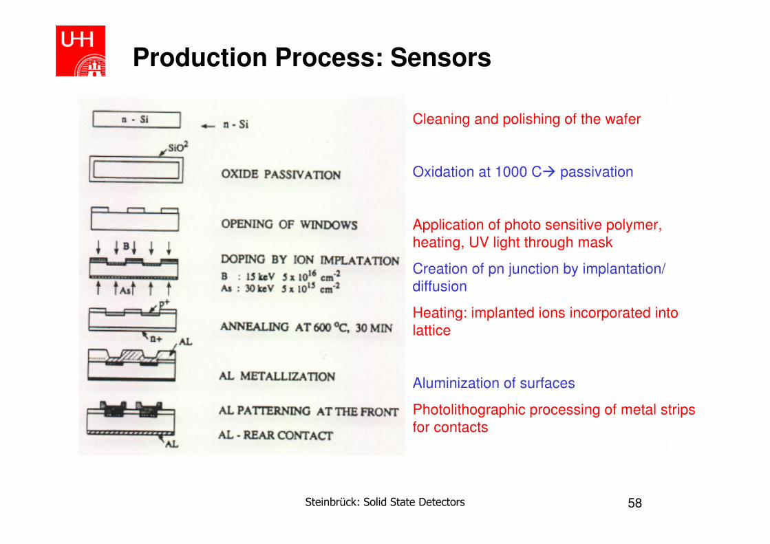
Production Process: Sensors
Cleaning and polishing of the wafer
Oxidation at 1000 C passivation
Application of photo sensitive polymer,
heating, UV light through mask
Creation of pn junction by implantation/
diffusion
Heating: implanted ions incorporated into
lattice
Aluminization of surfaces
Photolithographic processing of metal strips
for contacts
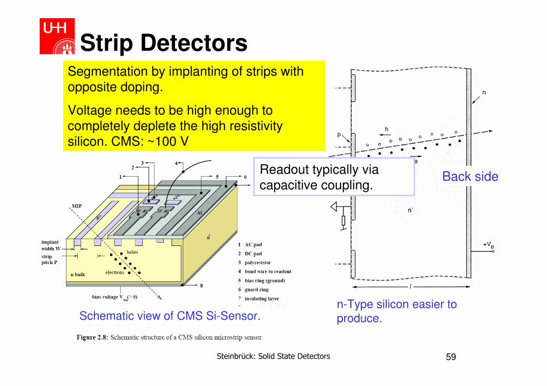
Steinbrück: Solid State Detectors 59
Strip Detectors
Back side
n-Type silicon easier to
produce.
Segmentation by implanting of strips with opposite doping.
Voltage needs to be high enough to completely deplete the high resistivitysilicon. CMS: ~100 V
Readout typically via capacitive coupling.
Schematic view of CMS Si-Sensor.

Steinbrück: Solid State Detectors 60
Single Sided Strip Readout
p+ readout strips
metallization (Al)
readout electronics
Ionizing particle
n+ silicon
metallization (Al)Reverse bias voltage
p+ readout:
• direct collection of holes
• both holes and electrons contribute to
current due to induction
Steinbrück: Solid State Detectors 61
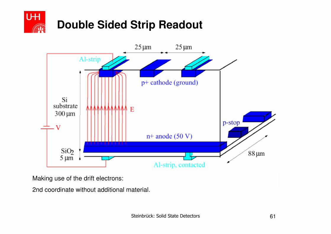
Double Sided Strip Readout
Making use of the drift electrons:
2nd coordinate without additional material.

Steinbrück: Solid State Detectors 62
Strip Detectors: Spatial Resolution
Digital readout:
Resolution given by
Analog readout:
Improved resolution σ<<p possible using center-of-gravity of charge distribution
Resolution limited by transverse diffusion of charge carriers
Typical values for Silicon: σ~5-10 µm
Typical pitch p=25-150 µm
12
4/
3
1)(
Resolution
:12
3
2/
2/
2
p
p
p
p
dxxx
xx
p
p
p
x
==
−
=−=
=
∫−
σ

Steinbrück: Solid State Detectors 63
Silicon Detectors:
Larger Systems

0.001
0.01
0. 1
1
10
100
2010 2005 2000 1995 1990 1985 1980
Year of operation
1980 NA1 1981 NA1 1 1982 NA1 4 1990 Mark II 1990 DELPHI 1991 ALEP H
1991 OPAL 1992 CD F 1993 L3 1998 CLEO III 1999 BABA R 2001 CDF-II 2006 ATLA S 20066 CM S
Sil
ico
n A
rea
[m
2]
History of Silicon Detectors
CMS

Steinbrück: Solid State Detectors 65
Examples: Detectors (CMS)
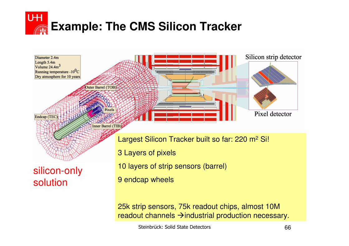
Steinbrück: Solid State Detectors 66
Example: The CMS Silicon Tracker
Largest Silicon Tracker built so far: 220 m2 Si!
3 Layers of pixels
10 layers of strip sensors (barrel)
9 endcap wheels
25k strip sensors, 75k readout chips, almost 10M readout channels industrial production necessary.
silicon-only solution

Steinbrück: Solid State Detectors 67
CMS Module Production
Si modules are precisely glued using a robot (gantry). Tolerances few µm!

Steinbrück: Solid State Detectors 68
The CMS Inner Barrel Detector under
Construction

Steinbrück: Solid State Detectors 69
The CMS detector from above

Steinbrück: Solid State Detectors 70
Insertion of the CMS Tracker

Steinbrück: Solid State Detectors 71
Insertion of one of the Endcap Silicon Detectors

Steinbrück: Solid State Detectors 72
Special Detectors: CMS Silicon Pixel Detector
• Segmentation in both directions Matrix
• Readout electronics with identical geometry
• Contacts using “bump bonding” technique
• Using soft material (indium, gold)
• Complex readout architecture
• real 2D hits
use in LHC experiments

Steinbrück: Solid State Detectors 73
The CMS Pixel Detector II• The inner layers feature:
• high multiplicity
• good spatial resolution needed (vertex finding)
Pixel good.
3 layers
Steinbrück: Solid State Detectors 74
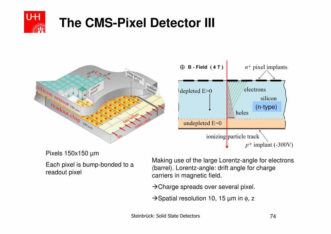
Pixels 150x150 µm
Each pixel is bump-bonded to a
readout pixel
Making use of the large Lorentz-angle for electrons
(barrel). Lorentz-angle: drift angle for charge
carriers in magnetic field.
Charge spreads over several pixel.
Spatial resolution 10, 15 µm in φ, z
The CMS-Pixel Detector III
(n-type)

Steinbrück: Solid State Detectors 75
The CMS-Pixel Detector:
Installation of Barrel Detector

Steinbrück: Solid State Detectors 76
The CMS-Pixel Detector: Barrel Installed
Steinbrück: Solid State Detectors 77
Other Technologies

Steinbrück: Solid State Detectors 78
Charged Coupled Devices
CCD principle of operation
-“analog shift register“
- many pixels – small no. read channels
- excellent noise performance (few e), but
small charge
- small pixel size (e.g. 22x22 µm2)
- slow (many ms) readout time
- sensitive during read-out
- radiation sensitive
used at SLC best vertex detector so far
with 3x108 pixels !!!
bbZ →0

Steinbrück: Solid State Detectors 79
Charged Coupled Devices: Examples
Fully depleted CCD (based on drift chamber principle) – astronomy XXM-Newtonxxx
L. Strüder, IEEE-Nucl. Sci. Symposium (Rome 2004)
elemental analysis of TYCHO supernova remnant:
XMM-Newton satellite

Steinbrück: Solid State Detectors 80
Si Drift Chambers
• Principle: anode position + drift time give 2 coordinates
• Capacitance relatively small (noise)
• Resolution ~10µm for 5-10 cm drift length
• dE/dx (STAR heavy ion)
• Drift velocity has to be well known
Need to reduce trapping
• Problems with radiation damage

Steinbrück: Solid State Detectors 81
Monolytic Pixel Detectors
Idea: radiation detector + amplifying +
logic circuitry on single Si-wafer
- dream! 1st realisation already in 1992
- difficult : Det. Si != electronics Si
- strong push from ILC minimum
thickness, size of pixels and power !
- so far no large scale application in
research (yet), but already used in
beam telescope at CERN
CMOS Active Pixels
(used in commercial CMOS cameras)
Principle:
- technology in development – with many
interesting results already achieved
example: MIMOSA (built by IReS-
Strasbourg; tests at DESY + UNIHH)
3.5 cm2 produced by AMS (0.6mm)
14 mm epi-layer, (17mm)2 pixels
4 matrices of 5122 pixels
10 MHz read-out ( 50ms)
120 mm thick
output
reset transistor
collectingnode
not depleted
Steinbrück: Solid State Detectors 82
Readout Electronics/
Noise
Steinbrück: Solid State Detectors 83
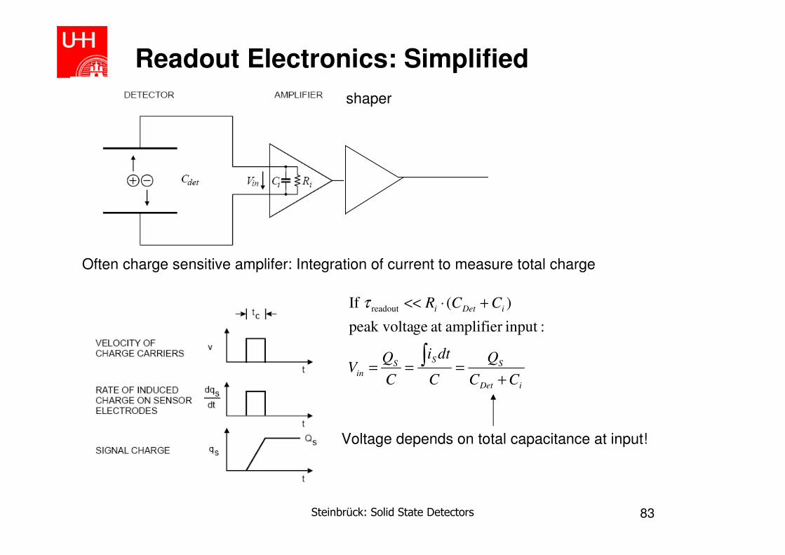
Readout Electronics: Simplified
shaper
Often charge sensitive amplifer: Integration of current to measure total charge
iDet
SSSin
iDeti
CC
Q
C
dti
C
QV
CCR
+===
+⋅<<
∫
:inputamplifier at gepeak volta
)( If readoutτ
Voltage depends on total capacitance at input!

Steinbrück: Solid State Detectors 84
Readout Electronics: Noise Simplified
The peak amplifier signal voltage is inversely proportional to the total capacitance at the
input of the amplifier, i,e. the sum of
• detector capacitance
• input capacitance of the amplifier
• any stray capacitances
Assume an amplifier with noise voltage at the input. Then the Signal/Noise is given by
This result in general applies to systems that measure signal charge.
smaller features are advantageous with respect to noise: Pixel.
C
1~
v
V
N
S
n
S=
SV
nv

Steinbrück: Solid State Detectors 85
Tracks
Momentum Measurement
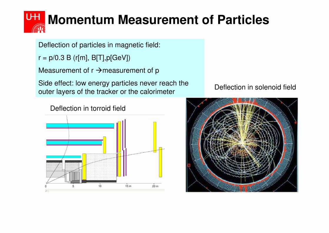
Momentum Measurement of Particles
Deflection of particles in magnetic field:
r = p/0.3 B (r[m], B[T],p[GeV])
Measurement of r measurement of p
Side effect: low energy particles never reach the outer layers of the tracker or the calorimeter
Deflection in solenoid field
Deflection in torroid field
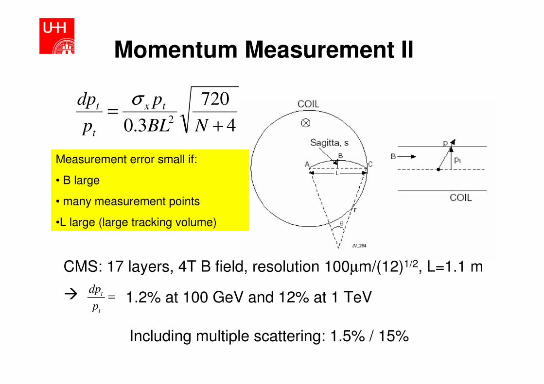
Momentum Measurement II
4
720
3.0 2 +=
NBL
p
p
dp tx
t
t σ
CMS: 17 layers, 4T B field, resolution 100µm/(12)1/2, L=1.1 m
Measurement error small if:
• B large
• many measurement points
•L large (large tracking volume)
=t
t
p
dp1.2% at 100 GeV and 12% at 1 TeV
Including multiple scattering: 1.5% / 15%
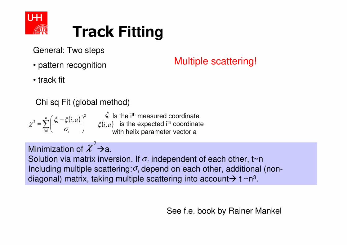
Track Fitting
Chi sq Fit (global method)
( )2
1
2 ,∑
=
−=
n
i i
i ai
σ
ξξχ
iξ Is the ith measured coordinate
is the expected ith coordinate
with helix parameter vector a( )ai,ξ
See f.e. book by Rainer Mankel
Minimization of a.Solution via matrix inversion. If independent of each other, t~nIncluding multiple scattering: depend on each other, additional (non-diagonal) matrix, taking multiple scattering into account t ~n3.
2χ
iσ
iσ
General: Two steps
• pattern recognition
• track fit
Multiple scattering!
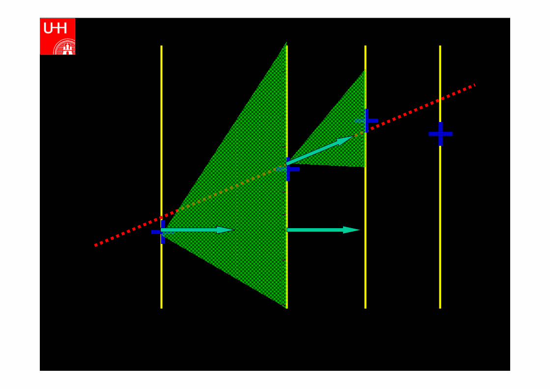
Track Fitting II: Kalman Filter
Kalman Filter:
• local, iterative method
• from outside inwards
• initial assumption for track parameter + error (covariance matrix)
• propagation of track to next layer
• calculation of new track parameters using hits + errors and track + errors (including multiple scattering)
• propagation to next layer, etc.
• t~n
• combined pattern recognition and track fit
• can be used same algorithm to reconstruct tracks in several sub-detectors (i.e. tracking chambers, muon system)
• can be nicely implemented in object oriented software
Steinbrück: Solid State Detectors 90
+
++ +

Steinbrück: Solid State Detectors 91
Summary• Solid state detectors play a central role in modern high energy and photon physics
• Used in tracking detectors for position and momentum measurements of charged
particles and for reconstruction of vertices (specially pixel detectors)
• By far the most important semiconductor: Silicon, indirect band gap 1.1 eV, however:
3.6 eV necessary to form eh pair
• Advantages Si: large yield in generated charge carriers, fine segmentation, radiation tolerant, mechanically stable, …
• Working principle (general) diode in reverse bias (pn junction)
• Important: S/N has to be good. Noise ~1/C for systems that measure signal charge
smaller feature sizes are good. Pixel!
• Radiation damage influences the material properties of the Si:
vacancies and interstitial atoms new energy levels in the band gap direct excitation possible Increase in leakage current trapping reduction in charge collection efficiency
• Most track finding and fitting algorithms minimize χ2 of tracks, Kalman filter commonly used

Steinbrück: Solid State Detectors 92
ReferencesGeneral detectors:• W.R. Leo: Techniques for Nuclear and Particle Physics Experiments: A How-to
Approach, Springer Verlag
•Semiconductor detectors:
• Lectures from Helmuth Spieler, LBNL: http://www-physics.lbl.gov/~spieler/
• H. Spieler: Semiconductor detector systems, Oxford University press
Pixel detectors:
• L. Rossi, P. Fischer, T. Rohe and N. Wermes Pixel Detectors: From Fundamentals
to Applications Springer 2995