solder joint reliability in electronics under shock …
TRANSCRIPT

SOLDER JOINT RELIABILITY IN ELECTRONICS UNDER SHOCK AND
VIBRATION USING EXPLICIT FINITE-ELEMENT SUB-MODELING
Except where reference is made to the work of others, the work described in this thesis is my own work or was done in collaboration with my advisory committee. This thesis does
not include proprietary or classified information.
_____________________________________________ Sameep Gupte
Certificate of Approval:
______________________________ ______________________________ Robert L. Jackson Pradeep Lall, Chair Assistant Professor Thomas Walter Professor Mechanical Engineering Mechanical Engineering ______________________________ ______________________________ George Flowers Joe F. Pittman Alumni Professor Interim Dean Mechanical Engineering Graduate School

SOLDER JOINT RELIABILITY IN ELECTRONICS UNDER SHOCK AND
VIBRATION USING EXPLICIT FINITE-ELEMENT SUB-MODELING
Sameep Gupte
A Thesis
Submitted to
the Graduate Faculty of
Auburn University
in Partial Fulfillment of the
Requirements for the
Degree of
Master of Science
Auburn, Alabama May 10, 2007

iii
SOLDER JOINT RELIABILITY IN ELECTRONICS UNDER SHOCK AND
VIBRATION USING EXPLICIT FINITE-ELEMENT SUB-MODELING
Sameep Gupte
Permission is granted to Auburn University to make copies of this thesis at its discretion, upon the request of individuals or institutions at their expense. The author reserves all
publication rights.
___________________________ Signature of Author
___________________________ Date of Graduation
iv
THESIS ABSTRACT
SOLDER JOINT RELIABILITY IN ELECTRONICS UNDER SHOCK AND
VIBRATION USING EXPLICIT FINITE-ELEMENT SUB-MODELING
Sameep Gupte
Master of Science, May 10, 2007 (B.E., Mumbai University, 2003)
151 Typed Pages
Directed by Pradeep Lall
Solder joint failure in electronic devices subject to shock and drop environment is
one of the key concerns for the telecommunications industry. The recent trend towards
miniaturization and increased functional density has resulted in decreasing the I/O pitch,
and thus increasing the chances of failure of the package under shock and vibration
environments. Solder joint failure occurs due to a combination of printed circuit board
(PCB) bending and mechanical shock during impact. Consequently, optimization of
package design is necessary to minimize the effects of shock during impact on the solder
interconnections.
In this present work, the modeling approaches for first-level solder interconnects
in shock and drop of electronics assemblies have been developed without any
assumptions of geometric or loading symmetry. The problem involves multiple scales

v
from the macro-scale transient-dynamics of electronic assembly to the micro-structural
damage history of interconnects. Previous modeling approaches include, solid-to-solid
sub-modeling [Zhu, et. al. 2001] using a half test PCB board and shell-to-solid sub-
modeling technique using a quarter symmetry model [Ren, et. al. 2003, 2004]. Inclusion
of model symmetry saves computational time but targets primarily symmetric mode
shapes. The modeling approach proposed in this paper enables prediction of both
symmetric and anti-symmetric modes. Approaches investigated include, smeared
property models, Timoshenko-beam element models, explicit sub-models, and
continuum-shell models. Transient dynamic behavior of the board assemblies in free and
JEDEC drop has been measured using high-speed strain and displacement measurements.
Model predictions have been correlated with experimental data. Two failure prediction
models namely the Timoshenko-Beam Failure Model and the Cohesive Zone Failure
Model have also been developed to predict the location and mode of failure in the solder
interconnections in PCB assemblies subject to drop impact.

vi
ACKNOWLEDGEMENTS
I would like to thank my advisor, Dr. Pradeep Lall, for his guidance, patience and
constant encouragement. Completion of the thesis would not have been possible without
his help. I would also like to acknowledge and thank the National Science Foundation for
their financial support. I also wish to extend my gratitude to Dr. George Flowers and Dr.
Robert Jackson for serving on my thesis committee and examining my thesis.
I would also like to thank all my friends and colleagues for their support and
understanding. Finally, many thanks go to Sanket, Pradnya and my parents for their
unwavering encouragement and love.

vii
Style manual or journal used Graduate School: Guide to Preparation and Submission of
Theses and Dissertations
Computer software used Microsoft Office 2003, Ansys 9.0, Altair Hyperworks 7.0,
Abaqus 6.6
viii
TABLE OF CONTENTS
LIST OF FIGURES x
LIST OF TABLES xv
CHAPTER 1 INTRODUCTION 1
CHAPTER 2 LITERATURE REVIEW 5
2.1 Experimental Techniques 5
2.2 Finite Element Simulations 10
CHAPTER 3 MODELING METHODOLOGY FOR DROP SIMULATIONS 18
3.1 Overview 18
3.2 Drop Simulation Methodology 27
3.3 Choice of Time Integration Formulation 29
3.4 Element Formulations and Characteristics 34
CHAPTER 4 FINITE ELEMENT MODELS FOR DROP SIMULATION 41
4.1 Smeared Property Global Model 41
4.2 Conventional Shell-Beam Model 50
4.3 Continuum Shell-Beam Model 57
4.4 Correlation of Predicted Peak Relative Displacement and Strain Histories 65
4.5 Error estimation in incorporating symmetry based models 70

ix
4.6 Solder Interconnect Strain Histories in the Global Model 70
4.7 Explicit Sub-model for Drop Simulation 72
4.8 Solder Interconnect Strain Histories in the Local Model 76
4.9 Susceptibility to Chip Fracture 87
CHAPTER 5 FAILURE PREDICTION MODELS 89
5.1 Overview 89
5.2 Timoshenko-Beam Failure Model 90
5.3 Cohesive Zone Failure Model 92
5.4 Modeling Approach and Modeling Correlations 103
CHAPTER 6 SUMMARY AND CONCLUSIONS 121
BIBLIOGRAPHY 123

x
LIST OF FIGURES Figure 1 State of the art modeling techniques. 11
Figure 2 Modeling Methodology. 19
Figure 3 Interconnect array configuration for 95.5Sn4.0Ag0.5Cu and 63Sn37Pb Test
Vehicles. 22
Figure 4 TABGA Test Board. 22
Figure 5 PCB assembly subject to 90-degree free vertical drop. 24
Figure 6 PCB assembly subject to 0-degree JEDEC drop. 24
Figure 7 Measurement of initial angle prior to impact. 25
Figure 8 Test board with target points to measure relative displacement. 25
Figure 9 High speed image analysis to capture displacement and velocity. 26
Figure 10 Transient-strain and continuity for determination of component failure. 26
Figure 11 90-degree free vertical drop. 28
Figure 12 Zero-degree horizontal JEDEC Drop. 28
Figure 13 Various element formulations employed to create the explicit models. 40
Figure 14 Typical architecture for TABGA package. 42
Figure 15 Schematic of 90-degree free vertical drop. 43
Figure 16 Schematic of Zero-Degree JEDEC Drop. 43
Figure 17 PCB modeled using shell (S4R) elements and CSP using smeared properties. 46

xi
Figure 18 Correlation of Transient Mode-Shapes for Smeared Element Model during
Free Vertical Drop. 51
Figure 19 Correlation of transient mode-shapes for Smeared Element Model during
JEDEC Drop. 52
Figure 20 Solder interconnection layout modeled using Timoshenko Beam elements. 54
Figure 21 Printed-Circuit assembly with Timoshenko-Beam Element interconnects and
Conventional Shell-Elements. 54
Figure 22 Correlation of transient mode-shapes for Conventional-Shell Timoshenko-
Beam Model during free vertical drop. 58
Figure 23 Correlation of transient mode-shapes for Conventional-Shell Timoshenko-
Beam Model during JEDEC Drop. 59
Figure 24 Solder interconnection layout modeled using Timoshenko Beam elements. 62
Figure 25 Printed-Circuit assembly with Timoshenko-Beam Element interconnects and
Continuum Shell-Elements. 62
Figure 26 Correlation of transient mode-shapes for Continuum-Shell
Timoshenko-Beam Model during free vertical drop. 63
Figure 27 Correlation of transient mode-shapes for Continuum-Shell Timoshenko-
Beam Model during JEDEC Drop. 64
Figure 28 Correlation between experimental relative displacement of board assembly
at 2.4 ms with model predictions under zero-degree JEDEC drop-test. 69
Figure 29 Correlation between experimental relative displacement of board assembly
at 4.5 ms with Model Predictions under 900 free drop-test. 69

xii
Figure 30 Stress distribution in the Timoshenko-Beam solder interconnects subject to
JEDEC drop for the Conventional Shell-Beam Model. 71
Figure 31 Representation of solder interconnection array. 73
Figure 32 Timoshenko-Beam Element with Conventional-Shell Model prediction of
transient strain history at the package corner solder interconnects during 0°
JEDEC-Drop. 74
Figure 33 Timoshenko-Beam Element with Conventional-Shell Model Prediction of
transient strain history in the solder interconnects located in the die shadow
region during 0° JEDEC-Drop. 74
Figure 34 Solder interconnection layout in Explicit Sub-model with a combination
hexahedral-element corner interconnects and Timoshenko-Beam Element
interconnects. 77
Figure 35 Local Explicit Sub-Model with hexahedral-element corner interconnects,
Timoshenko-Beam Element interconnects and PCB meshed with
hexahedral reduced integration-elements. 78
Figure 36 Strain histories in the local model corresponding to Conventional Shell
Timoshenko-beam global model during JEDEC-drop at various time
intervals. 80
Figure 37 Strain histories in the local model corresponding to Conventional Shell
Timoshenko-beam global model during free vertical drop at various time
intervals. 81

xiii
Figure 38 Global-Local explicit Sub-Model predictions of transient logarithmic shear
strain, LE12, in the solder interconnect of one of the chip-scale packages
on the printed circuit board assembly during JEDEC Drop. 82
Figure 39 Global-Local Explicit Sub-Model predictions of transient logarithmic shear
strain, LE23, in the solder interconnect of one of the chip-scale packages
on the printed circuit board assembly during JEDEC Drop. 83
Figure 40 Global-Local Explicit Sub-Model predictions of transient logarithmic shear
strain, LE12, in the solder interconnect of one of the chip-scale packages on
the printed circuit board assembly during Free Drop. 84
Figure 41 Global-Local Explicit Sub-Model predictions of transient logarithmic shear
strain, LE23, in the solder interconnect of one of the chip-scale packages
on the printed circuit board assembly during Free Drop. 85
Figure 42 Cross-section of corner solder interconnect in the failed samples showing
higher susceptibility of the samples to fail at the package-to-solder
interconnect interface or the solder-to-printed circuit board interface. 86
Figure 43 Transient stress history in the silicon chip. 88
Figure 44 Transient stress history in chip top and bottom surfaces. 88
Figure 45 Brittle interfacial failure observed in the solder interconnections at the
package side and the PCB side. 89
Figure 46 Solder joint array tensile test configuration [Darveaux et al. 2006]. 91
Figure 47 Stress-Strain response of solder ball sample subject to tensile loading at
various strain rates [Darveaux et al. 2006]. 91
Figure 48 Traction components at the interface. 96

xiv
Figure 49 Normal traction as a function of un with ut ≡ 0 [Needleman 1990]. 98
Figure 50 Different forms of Traction-Separation laws. 99
Figure 51 Linear Traction-Separation response for cohesive elements [Abaqus 2006]. 102
Figure 52 Interconnect array configuration for Test Vehicle. 104
Figure 53 Printed-Circuit assembly with Timoshenko-Beam Element interconnects
and Conventional Shell-Elements. 105
Figure 54 Explicit Sub-Model with hexahedral-element corner interconnects,
Timoshenko-Beam Element interconnects and PCB meshed with
hexahedral reduced integration-elements with layer of cohesive elements
at the solder joint-copper pad interface at both PCB and package side. 106
Figure 55 Drop-orientation has been varied from 0° JEDEC-drop to 90° free-drop. 108
Figure 56 Correlation of transient mode shapes during Free Drop. 110
Figure 57 Correlation of transient mode shapes during JEDEC Drop. 111
Figure 58 Explicit Sub-modeling technique employed at all component locations. 114
Figure 59 Time History of the displacement at the boundary nodes of the global
model and the explicit sub-model. 114
Figure 60 Number of drop to failure as a function of maximum peak strain in the
cohesive element at different component locations for JEDEC Drop. 119

xv
LIST OF TABLES Table 1 Test Vehicle. 21
Table 2 Components modeled in the global model and their respective element types. 37
Table 3 Components modeled in the local model and their respective element types. 37
Table 4 Characteristics of element types used. 38
Table 5 Material properties for individual layers of TABGA package. 44
Table 6 Element types used in smeared property models. 47
Table 7 Dimensions and masses of individual layers in the package. 47
Table 8 Comparison of actual and simulated component masses using Smeared
Property Models. 47
Table 9 Element types used in Conventional Shell-Beam Model. 55
Table 10 Comparison of actual and simulated component masses using Conventional
Shell-Beam Model. 55
Table 11 Element types used in Continuum Shell-Beam Model. 61
Table 12 Comparison of actual and simulated component masses using Continuum
Shell-Beam Model. 61
Table 13 Correlation of peak-strain values from model predictions versus experiments
for 90-Degree Free-Drop. 66

xvi
Table 14 Correlation of peak relative displacement values between various explicit
models. 67
Table 15 Computational efficiency for various explicit models subject to free drop. 68
Table 16 Computational efficiency for various explicit models subject to JEDEC drop. 68
Table 17 Estimated error in prediction of solder interconnect stress in using diagonal
symmetry model for Conventional Shell Beam Model subject to JEDEC drop. 71
Table 18 Estimated error in prediction of solder interconnect stress in using half
symmetry model for Continuum Shell-Beam Model subject to free drop. 71
Table 19 Element types used in the Explicit Sub-Model. 77
Table 20 Test Vehicle. 104
Table 21 Correlation of peak-strain values from Timoshenko-Beam Failure Model
predictions versus experiments for 90-Degree free-drop. 112
Table 22 Correlation of peak relative-displacement values with high-speed
experimental data on zero-degree JEDEC Drop (mm). 112
Table 23 Correlation of peak-strain values from model predictions versus experiments
for zero-degree JEDEC-Drop. 113
Table 24 Correlation of Timoshenko-Beam Failure Model predictions with
experimental data for solder interconnect failure location for JEDEC Drop. 115
Table 25 Correlation of Timoshenko-Beam Failure Model predictions with
experimental data for solder interconnect failure location for Free Drop. 116
Table 26 Correlation of explicit cohesive Sub-Model predictions with experimental
data for solder interconnect failure location for Free Drop. 117

1
CHAPTER 1
INTRODUCTION Solder joint failure in electronic products subject to shock and vibration is a
dominant failure mechanism in portable electronics. Increase product-functionality
concurrent with miniaturization has placed electronic interconnects in close proximity of
the external impact surfaces of electronic products. Transient mechanical shock and
vibration may be experienced during shipping, transportation, and normal usage.
Presently, product-level evaluation of drop and shock reliability depends heavily
on experimental methods. System-level reliability response is influenced by various
factors such as the drop height, orientation of drop, and variations in product design [Lim
2002, 2003]. The complex physical architecture typical of electronic products, makes it
expensive, time-consuming and difficult to test solder joint reliability and dominant
failure interfaces in each shock-orientation. Faster-cycle times cost and time-to-market
constraints limit the number of configurations that can be fabricated and tested.
Additionally, the small size of the solder interconnections makes it difficult to mount
strain gages at the board-joint interface in order to measure field quantities and
derivatives of field quantities such as displacement, and strain. Currently, the JEDEC
drop-test [JESD22-B111 2003] is used to address board-level reliability of components,

2
which involves subjecting the board to a 1500g, 0.5 ms pulse in the horizontal
orientation. It is often difficult to extrapolate product level performance from the board
level JEDEC test since, product boundary conditions and impact orientation may be
different from the test configuration.
In this research effort, the use of beam-failure models and cohesive-zone failure
models for predicting first-level interconnect reliability has been investigated. Multi-
scale nature of the shock model requires capture of transient dynamics at system level
simultaneously with transient stress histories in the metallization interconnect pad and
chip-interconnects. Previous approaches include, solid-to-solid sub-modeling [Zhu 2001,
2003] using a half test PCB board, shell-to-solid sub-modeling technique using a quarter
symmetry model [Ren et al. 2003, 2004]. Inclusion of model symmetry saves
computational time but targets primarily symmetric mode shapes. Use of equivalent layer
models [Gu et al. 2005a, b], smeared property models [Lall et al. 2004, 2005],
Conventional shell with Timoshenko-beam Element Model and the Continuum Shell with
Timoshenko-Beam Element Model [Lall 2006] has been made to represent the solder
joints and study their response under drop impact in an attempt to achieve computational
efficiency.
Reliability of BGA packages greatly depends upon strength with which the solder
joint is attached to the package. Ball shear and ball pull testing methods are currently
used to determine the solder joint strength. Ductile-brittle transition from bulk solder to
IMC failure was observed in the miniature Charpy test [Date et al. 2004] on increasing
the shear speed from 0.2 mm/s to 1 m/s. The study of interface failures between the
solder joint and the package or PCB side at high strain rates was studied by carrying out

3
tensile tests of solder joint arrays [Darveaux et al. 2006]. Strain rates used in these tests
were from 0.001/s to 1/s.
In this work, the Conventional shell-Timoshenko Beam Element Model and the
Global-Local Explicit Sub-model have been used to simulate the drop phenomenon,
without any assumptions of symmetry to predict the transient dynamic behavior and
interconnect stresses. In the first approach, drop simulations of printed circuit board
assemblies in various orientations have been carried out using beam-shell modeling
methodologies without any assumptions of symmetry. This approach enables the
prediction of full-field stress-strain distribution in the system over the entire drop event.
The modeling approach proposed in this study enables prediction of both symmetric and
anti-symmetric modes without the penalty of decreased time-step size. A Timoshenko-
Beam failure model based on the critical equivalent plastic strain value is used as a
failure proxy to predict the failure mechanisms in the solder interconnections. The
proposed method’s computational efficiency and accuracy has been quantified with data
obtained from the actual drop-test. Transient dynamic behavior of the board assemblies in
free and JEDEC drop has been measured using high-speed strain and displacement
measurements. Relative displacement and strain histories predicted by modeling have
been correlated with experimental data. Failure data obtained by solder joint array tensile
tests on ball grid array packages is used as a failure proxy to predict the failure in solder
interconnections modeled using Timoshenko beam elements in the global model.
In the second approach, cohesive elements [Towashiraporn 2005, 2006] have
been incorporated in the local model at the solder joint-copper pad interface at both the
PCB and package side. Cohesive elements have been incorporated in the local model at

4
the solder joint-copper pad interface on the PCB and package side. Use of cohesive zone
modeling enabled the detection of failure initiation and propagation leading to IMC
brittle failure in PCB assemblies subject to drop impact. Data on solder interconnect
failure has been obtained from free-drop and JEDEC-drop tests. Strains, accelerations
and other relevant data have been analyzed using high speed data acquisition systems.
Ultra high-speed video at 50,000 frames per second has been used to capture the
deformation kinematics.

5
CHAPTER 2
LITERATURE REVIEW
Solder joint failure in electronic assemblies subject to shock and vibration is of
major concern to the portable electronics industry. Recently, significant research has been
focused to predict the solder joint reliability in electronic packages under harsh
mechanical environments. Experimental techniques, analytical modeling and simulations
are primarily used to evaluate the dynamic response of the system subject to drop impact.
A thorough study of the literature published in this area is necessary to understand the
various methodologies that have been employed to address the reliability issues.
2.1 Experimental Techniques Solder joint reliability performance in electronic products in harsh mechanical
environments such as drop impact is generally conducted using experimental techniques
at the board level and the product level. Product level drop tests on completed products
provide a more realistic scenario of the level of shock experienced by the solder
interconnections. Product level evaluation of drop and shock reliability depends heavily
on experimental methods. Board level drop testing mimics the real-life drop impact
conditions and are more controllable as compared to product level drop tests. However,
board level testing does not take into account the interaction between the PCB, plastic
casing and other internal components of the product. Also the standardized JEDEC drop

6
tests do not take into account the various drop orientations with which the product may
strike the impacting surface or multiple impacts due to rebounding. Shock response
experienced by the PCB in product level drop can be used to set up the board level drop
to reproduce the real time conditions that the package components and solder joints
undergo during actual drop. In order to address these issues, extensive experimental tests
are carried out to understand the variations in the dynamic responses of the PCB subject
to board or product level drop.
Lim et al. [2003] carried out product level and board level drop tests on a mobile
phone and its PCB respectively. In these tests, the test vehicle was gripped in various
orientations and allowed to strike the impacting surface under gravity forces from desired
heights using a drop tower. Results indicated additional levels of deformation of the PCB
in case of product level drop due to severe rebound impact. Also, drop impact responses
of various mobile phones and personal digital assistants (PDAs) were carried out at
various orientations from a drop height of one meter and accelerations, strains and impact
forces were measured. Maximum PCB strains and accelerations were recorded in product
level drop in the horizontal direction Wu et al. [1998] carried out product level drop tests
on a customized drop tester equipped with a drop control mechanism to control drop
orientation and achieve a high degree of reliability. Xie et al. [2003] performed free fall
board level and product level drops of area array LGA packages and measured the
accelerations at the board and package side. It was found that the accelerations obtained
in case of phone drop were much lower than those in the corresponding board level drop.
However, FEA results showed higher values for PCB warpage and maximum plastic
strain in the solder joints in case of product level drop. Dynamic shock testing of test

7
boards [Geng 2005] was carried out on a four point bend like shock test fixture at fixed
and incremental shock levels and in-situ continuity monitoring of the solder joints was
carried out to detect failure. In order to replicate the shock experienced by the PCB inside
an actual PC motherboard, experimental modal analysis was carried out on the
motherboard and its fundamental frequency was obtained. The test setup was then
adjusted to match the fundamental frequencies of the system with the tested motherboard.
Tee et al. [2004] conducted board level drop test in accordance with the JEDEC
test standards [2003] by mounting a TFBGA package in the centre of the PCB.
Comprehensive dynamic responses of the PCB and the solder joints such as
accelerations, strains and resistances were measured and analyzed using a multi-channel
real-time electrical monitoring system. The study suggested a correlation between the
dynamic strains in the PCB caused by the multiple flexing of the PCB and mechanical
shock and the resulting solder joint fatigue failure. Similarly, Mishiro et al. [2002]
showed correlation between the PCB strains and solder bump stresses by performing drop
tests of BGA packages mounted on a motherboard. The study also showed the
dependence of solder joint stress on package design and structure and stress reduction by
including underfills. Lall et al. [2004, 2005] performed controlled drop tests of BGA and
CSP packages from different heights in the vertical direction. Strain gages were mounted
at the various component locations at both at PCB side and the package side. Strain and
continuity data were obtained during the drop event with the help of a high-speed data
acquisition system which recorded data at the rate of around 5 million samples per
second. In addition, the drop test was monitored with ultra-high speed video camera at
40,000 frames per second. Various experimental parameters such as relative

8
displacements, strains, velocities, accelerations etc were acquired simultaneously. Failure
analysis of the failed test specimen showed solder joint failures at the package and board
interfaces and copper-trace cracking.
Shah et al. [2004] conducted displacement controlled board level bend tests on
BGA packages at displacement rates corresponding to dynamic loading using a servo-
hydraulic mechanical test system. The electrical connectivity of the solder joints was
monitored using a daisy chained structure. Flip chip on board (FCOB) assemblies were
subjected to vibration fatigue tests [Pang et al. 2004] for constant and varying G-level
vibration tests to predict solder joint fatigue life. Clamped-clamped boundary conditions
were imposed on the board and the tests were carried out on an electrodynamic shaker.
Wang et al. [2003] performed free-fall board drop test analysis in the horizontal direction
on FCOB assemblies using a shock test machine providing the half sine pulse for impact
excitation. Three-point bending and four-point bending tests [Shetty et al. 2003] were
carried out to investigate the fatigue failure of solder interconnects due to excessive
cyclic PCB bending and flexure which may occur due to drop impact. The tests were
carried out on a servo-hydraulic machine and the daisy-chained packages are
continuously monitored to detect failure.
Reliability of Ball Grid Array (BGA) packages greatly depends upon strength
with which the solder joint is attached to the package. Ball shear and ball pull testing
methods are currently used to determine the solder joint strength. Erich et al. [1999]
carried out shear tests on an Instron MTS at a shear rate of 0.5mm/min to study the
interfacial failure mechanisms of BGA solder joints. The various failure mechanisms
observed included pad peel, ductile bulk solder shearing and brittle fracture between the

9
solder and the pad. However, in actual drop events, the strain rate experienced by the
solder joints is of a much higher magnitude. Ductile-brittle transition from bulk solder to
IMC failure was observed in the miniature Charpy test [Date et al. 2004] on increasing
the shear speed from 0.2 mm/s to 1 m/s. Solder joint integrity was tested by subjecting
them to high speed impact using an Instron Micro Impactor [Wong et al., 2004] to obtain
fracture characteristics such as fracture strength and fracture energy upon impact. Various
solder materials with different pad finishes and mask designs were tested at static and
impact shear speeds of 50 and 600 micrometers/second. It was seen that the fracture
strength of the ductile bulk solder increased with shear speed while that of the brittle
inter-metallic compound (IMC) decreased with shear speed. This might explain the IMC
failures in solder joints subject to high strain rates during impact. Ong et al. [2004]
carried out testing of eutectic solder using Split Hopkinson Pressure Bars (SHPB) to
show the effect of higher strain rates on the dynamic properties of solder. Bansal et al.
[2005] performed high speed four point bend tests with strain rates greater than 5000
micro strains per second in accordance with IPC/JEDEC 9702 [2004] to mimic to brittle
fractures of flip chip BGA packages during PCB assembly operations with both leaded
and lead-free solder alloys and ENIG pad finishes. Results indicate that the strains to
failure decrease with increase in the strain rates. Shear tests at high strain rates similar to
those experienced by the solder joint during drop impact were carried out on BGA and
LGA packages to determine the package to board interconnection shear strength [Hanabe
et al. 2004]. The tests were performed on a servo hydraulic uniaxial MTS at low and high
cross-head speeds of 0.0033 mm/s and 0.5 mm/s to approximately replicate the shear
forces acting on the solder joints during thermal cycling and mechanical drop. The study
10
of interface failures between the solder joint and the package or PCB side at high strain
rates was studied by carrying out tensile tests of solder joint arrays [Darveaux et al.
2006]. Strain rates used in these tests were from 0.001/s to 1/s. The ductile to brittle
transition mode of failure at higher strain rates justifies the occurrence of the IMC
failures under impact loading.
2.2 Finite Element Simulations
Modeling and simulation of IC packages subject to shock and vibration are very
efficient tools for design analysis and optimization. Additionally, they are inexpensive,
less time consuming and require much less manpower as compared to actual
experimental techniques. They are very useful during the early prototype development
stages where it is not possible to test every design modification. Simulation techniques
are also needed to determine the potential PCB assembly failure modes as it is very
difficult to measure the stresses and strains developed in the solder joints during drop
test. A validated drop test model exhibiting relatively good correlation of dynamic
responses of the PCB with the experimental data can be very beneficial in design
enhancement and qualification of the electronic packages. Figure 1 shows the state of the
art modeling techniques employed to model the PCB assemblies.

11
Slice Model Symmetry Model Full PCB AssemblySlice Model Symmetry Model Full PCB Assembly
Figure 1 State of the art modeling techniques.

12
Tee et al. [2004] performed board level drop test simulations of 0.75 pitch TFBGA
packages using a three-dimensional quarter symmetry model on the basis of symmetry to
reduce the model size. The Input-G method [Tee et al. 2004] was used in the explicit
finite element solver ANSYS/LS-DYNA to simulate the drop impact by applying the
input acceleration pulse measured during the actual drop test to the corner screws of the
PCB. Solder joint failure at the solder-PCB pad interface using maximum normal peeling
stress as the failure proxy was predicted by the simulation results and was correlated with
experimental observations and failure analysis. A life prediction model was proposed for
QFN packages to estimate the number of drops to failure by Tee et al. [2003]. The effects
of various testing parameters such as drop orientation, drop height, and PCB bending on
the number of cycles to failure were studied. Pang et al. [2004] conducted finite element
analysis for the vibration tests of Flip Chip On Board (FCOB) assemblies to determine
the natural frequencies and mode shapes of the system under dynamic loading conditions.
The global-local beam model was incorporated in this analysis by modeling the PCB and
the chip with shell elements and the solder interconnections were represented by two-
node beam elements with equivalent solder joint stiffness. Quasi-static analysis and
dynamic drop test simulations using sub-modeling technique were modeled to predict the
fatigue life of the solder joints. Three-point bending simulations [Shetty et al. 2003] of
CSP packages were conducted using the global-local modeling methodology in ANSYS
to predict the effect of repetitive PCB bending on solder joint failure. A quarter symmetry
model was employed and appropriate boundary conditions were applied to simulate the
actual test. A reliability model was developed to predict the cycles to failure based on the
value of the average strain energy density in the critical solder joint in the local model.

13
Carroll et al. [2005] performed static and dynamic four point bending simulations to
study the relationship between PCB and solder joint strains and showed a higher
accumulation of plastic strain in the solder joints in case of dynamic bending tests as
compared to static bending tests. Solder joints were modeled using beam elements to
achieve computational efficiency and this approach was combined with the sub-modeling
technique to obtain detailed stress and strain values in the critical solder joints. Wang et
al. [2003] conducted two finite element analyses of the FCOB assemblies using the full
and the hybrid models respectively. The full model consisted of the FCOB assembly,
drop table, fixtures etc. and simulated the actual drop event. On the other hand, the hybrid
model consisted of only the PCB and the IC chips and the experimentally measured
displacement histories at the clamped edges of the PCB were applied as boundary
conditions in the simulation. The hybrid model exhibited better correlation than the full
model with respect to the experimental displacement and acceleration magnitudes.
Detailed modeling of every solder joint in the PCB assembly is computationally
challenging and expensive. Therefore, some methodologies need to be developed to
include all the solder joints in the simulation at no computational expense. Gu et al.
[2004, 2005] used equivalent layer models to represent the solder joints and simulate
their behavior under drop impact. The full equivalent layer model consisted of a single
three-dimensional continuum layer to represent all the individual solder joints. The
hybrid model consisted of combination of the continuum layer in the non-critical areas
and solder columns representing the solder interconnections in the critical areas. The
equivalent material properties for the continuum layer such as the elastic modulus,
density, Poisson’s ratio etc were determined by numerical three-point bending, torsion

14
and tension tests. These equivalent layers models showed a good level of accuracy with
the detailed global model and computational efficiency. Lall et al. [2004, 2005] simulated
the vertical free drop of CSP packages mounted on a PCB from a height of 6 feet. In
order to save processing time, the velocity of the board just before impact was calculated
based on the drop height and applied to all the nodes in the model as initial conditions.
The PCB was modeled using shell as well as solid elements while the components were
modeled using solid elements. Smeared property [Clech 1996, 1998] approach based on
the volumetric averaging method was used to derive the elastic properties for the
components. The simulation was carried out in ABAQUS/Explicit since explicit
formulation is suitable for modeling dynamic events occurring within a short time
interval. Good correlation was obtained with respect to the mode shapes, relative
displacement and strain time histories. Wong et al. [2002] illustrated the fundamental
mechanics and physics of a board level drop impact and the propagation of the stress
wave though the assembly. A quarter symmetry model was used to simulate the drop
impact of a PCB assembly. The global-local modeling methodology was incorporated in
which the global beam-shell model was run in Abaqus/Explicit while the sub-model
representing the critical solder ball was run in Abaqus/Standard based on the results of
the global model. Differential flexing between the PCB and the package and inertia
forces of the packages were found to be the dominant causes of failure. Shell-to-solid
sub-modeling applied to a quarter symmetry model under impact and other loading
conditions [Ren et al. 2003, 2004] was used in Abaqus/Explicit to reduce the
computational time required for simulation. To validate the global-local modeling
technique, Tan, et. al. [2005] modeled the PCB, solder interconnections and packages

15
with varying levels of detail to determine the deviation of results and its effect on
computational efficiency. Comparisons of reduced models namely the shell-beam model
and the shell-solid model with the detailed finely meshed solid model show reasonable
comparison in terms of displacement. However, the solder ball stress comparisons in the
reduced models showed poor correlation with the detailed model. Wu et al. [1998]
performed product-level drop simulations to study effects of drop impact such as housing
break, LCD cracking and structural disconnection. Free drop and ball bearing drop
simulations were carried out for cell phones and radios to predict the LCD cracking and
housing break based on the plastic strain values and validated with test results. Drop test
modeling of Fairchild 6 lead Micropak mounted on a board and end product casing was
carried out using implicit time formulation in ANSYS [Irving et al. 2004]. The
propagation of the stress wave generated due to impact travels from the product casing to
the PCB and finally to the solder joints resulting in failure. Piterassi et al. [2004]
simulated the response of PC motherboards to shock loads using the simple block
modeling and global property smearing approaches. Simplified block modeling involves
replacing the components having significant mass and stiffness concentrations with
simple homogeneous rectangular blocks. The global smeared approach involved
replacing the entire motherboard with an equivalent flat plate. The equivalent mass and
stiffness of the simplified blocks was determined by experimental or numerical three
point bending of the individual components. Shock response spectrum (SRS) and implicit
direct integration methods were used to evaluate the response due to shock loading and
correlated with experimental drop testing performed on a drop table or a shaker system.
Zhu et al. [2001] employed a global-local modeling technique to evaluate the reliability

16
of PCB assemblies subject to mechanical loading. A quarter symmetry global model is
used to simulate the three-point bending and the deformation and stress-strain distribution
of the PCB is obtained. The location of the critical package and solder joint is determined
from these results and is modeled as the local model with a fine mesh to obtain the
detailed stresses in the solder joint. Average strain energy density criterion is used to
estimate the number of cycles to failure. Syed et al. [2005] simulated a three point
bending test of a component level model to evaluate the equivalent stiffness of the
component. This model was built using solid elements and included all the layers of the
package along with the solder interconnections and the PCB and the effective modulus of
the board-package combination is obtained. The global model of the board is then created
with the components of equivalent mass and density and analyzed using the Input G
method. Damage initiation and progression in electronic assemblies subject to
mechanical shock was monitored using statistical pattern recognition, closed-form
models and leading indicators of damage prediction [Lall et al. 2006]. This alternate
approach to quantify damage does not require the continuous monitoring of the electrical
continuity to detect failure and can be applied to any generic electronic structure. Zhu et
al. [2004] performed board and product level drop simulations using the sequential
explicit-implicit and sub-modeling techniques and validated with experimental tests.
Effective plastic strain was chosen to be the failure criteria to determine the BGA solder
joint failure since it is accumulative in nature and not oscillatory as is the case with the
Von Mises stress. Towashiraporn et al. [2006] incorporated cohesive zone methodology
to model the brittle fracture failure at the solder joint-copper pad interface during drop
impact in ABAQUS/Explicit. Cohesive elements were placed at the solder joint-copper

17
pad interfaces at both the PCB and package side. The constitutive response of the
cohesive elements was based on a traction-separation behavior derived from fracture
mechanics. Damage initiation and evolution criteria are specified to ensure progressive
degradation of the material stiffness leading to cohesive element failure.

18
CHAPTER 3
MODELING METHODOLOGY FOR DROP SIMULATIONS
3.1 Overview
Board level drop simulation of electronic packages using finite element analysis
has proven to be a very useful qualitative tool to understand the transient dynamic
behavior of these assemblies under mechanical shock loading. This research project
focused on predicting the solder joint reliability in printed circuit board assemblies
subject to drop impact in various orientations from varying heights. Various element
formulations have been employed to model the individual components of the assembly.
Approaches investigated include smeared property models, conventional shell elements
with Timoshenko-beam elements, continuum shell elements with Timoshenko-beam
elements and the explicit sub-models. The explicit time integration formulation has been
used to simulate the drop event. The sub-modeling technique has been employed to study
the stress-strain distribution in the critical solder interconnection in detail. Shell-to-solid
sub-modeling technique has been employed to transfer the time history response of the
global model to the local model wherein displacement degrees of freedom from the
global model are interpolated to the local model and applied as boundary conditions.
Transient dynamic behaviors of the board assemblies in free vertical drop and horizontal
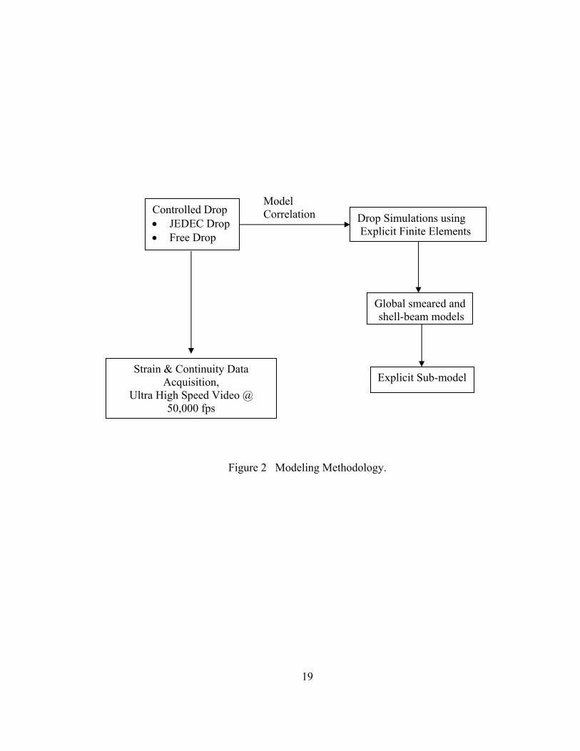
19
Figure 2 Modeling Methodology.
Strain & Continuity Data Acquisition,
Ultra High Speed Video @ 50,000 fps
Drop Simulations using Explicit Finite Elements
Global smeared and shell-beam models
Explicit Sub-model
Model CorrelationControlled Drop
• JEDEC Drop • Free Drop

20
JEDEC drops have been measured using high-speed strain and displacement
measurements. Models predictions have been correlated with experimental data such as
relative displacement and strain histories. The modeling approach used is briefly
summarized in Figure 2. Test boards were subjected to a controlled drop in both 0-degree
JEDEC drops and 90-degree free vertical drops at varying heights. Table 1 shows the
package attributes for the test vehicle. The test board employed was the 8 mm flex-
substrate chip scale packages, with 0.5 pitch and 132 solder interconnections. The layout
of the solder interconnections is shown in Figure 3. The printed circuit board was made
of FR-4 and its dimensions were 2.95 inches by 2.95 inches by 0.042 inches. There were
10 components mounted on the printed circuit board as illustrated in Figure 4. All the
components are on one side of the board. For the 8 mm CSP, conventional eutectic
solder, 63Sn/37Pb and lead-free solder balls 95.5Sn4.0Ag0.5Cu have been studied. In the
case of free drop in the 90-degree vertical orientation, a single weight was attached at the
top edge of the board to simulate the batteries generally located at the top of the device.
In case of horizontal drop, the board assemblies were subjected to the zero-degree
orientation JEDEC drop in accordance with the JESD22-B111 standard [2003] provided
by the JEDEC solid state technology association. The test board is mounted on a rigid
steel base plate using four connecting screws. The components mounted on the board are
facing downwards to ensure maximum deflection. The rigid base plate is then fixed to the
drop table and care is taken to ensure that there is no relative motion between them. The
drop table can be dropped from prescribed heights along two guide rails to strike the
impacting surface.

21
Table 1 Test Vehicle.
10mm
63Sn37Pb
8mm
62Sn36Pb2Ag
8mm
95.5Sn4.0Ag
0.5Cu
Ball Count 100 132 132
Ball Pitch 0.8 mm 0.5 mm 0.5 mm
Die Size 5 x 5 3.98 x 3.98 3.98 x 3.98
Substrate
Thickness 0.5 mm 0.1 mm 0.1 mm
Substrate Pad Dia. 0.3 mm 0.28 mm 0.28 mm
Substrate Pad
Type SMD Thru-Flex Thru-Flex
Ball Dia. 0.46 mm 0.3 mm 0.3 mm

22
10 mm, 100 I/O BGA 8mm 132 I/O BGA
Figure 3 Interconnect array configuration for 95.5Sn4.0Ag0.5Cu and 63Sn37Pb Test Vehicles.
Figure 4 TABGA Test Board.

23
The test board was subjected to a controlled drop from heights of 6 feet and 0.5 feet for
free drop (Figure 5) and JEDEC drop (Figure 6) respectively using a drop tower. Strain
gages were mounted at all the component locations at both the PCB and the package
sides to record the strain histories during the drop event. Strain and continuity data during
the drop event was acquired using a high speed data acquisition system at a sampling rate
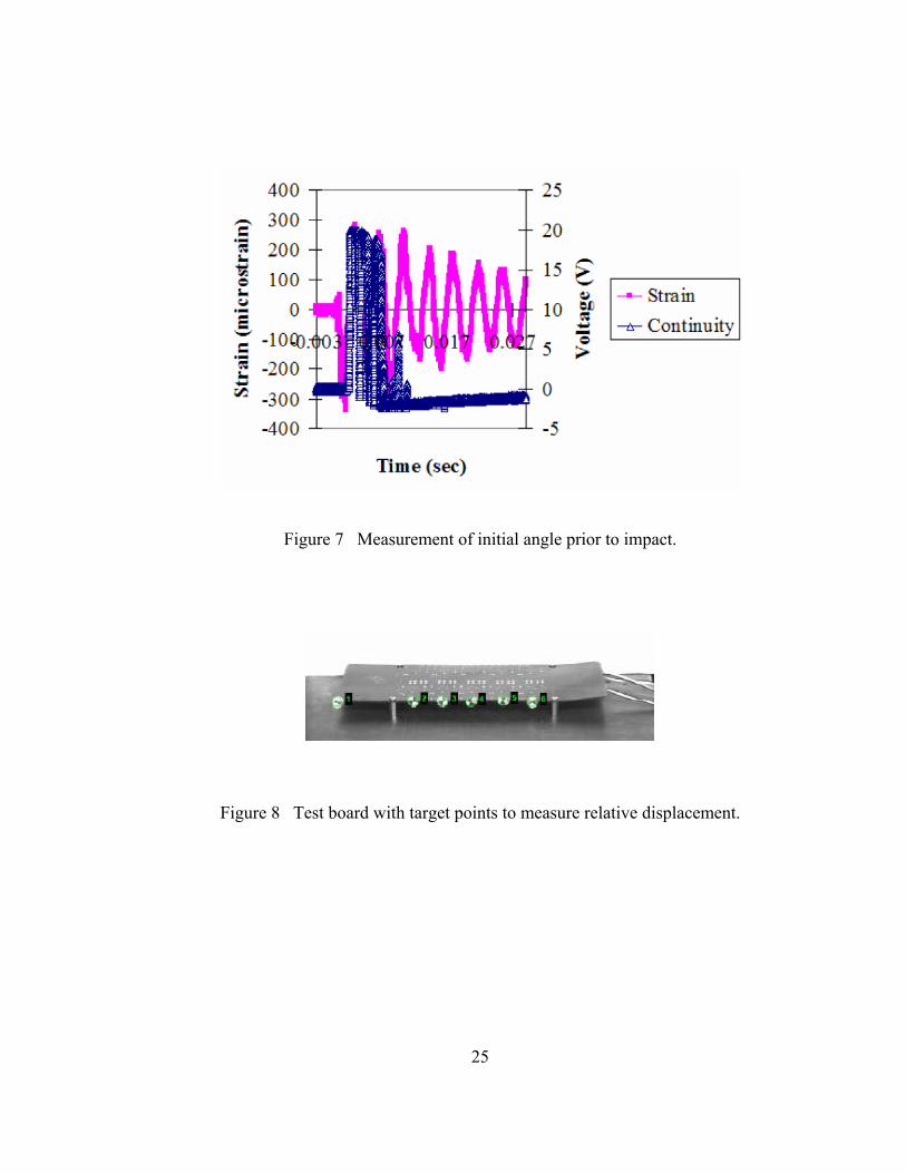
of 5 million samples per second to detect the component failure (Figure 7). The
components are daisy chained to monitor the failure of the interconnection during drop
test. In-situ monitoring of the failure detection is necessary because cracks that appear in
the material due to the flexing of the PCB during the drop event may close up when the
PCB returns to its original shape. In addition, the drop event was simultaneously
monitored using a high speed camera at 50,000 frames per second to study the
deformation kinematics of the assembly. The transient mode shapes captured using this
camera are used for correlation with the mode shapes obtained with simulation. Target
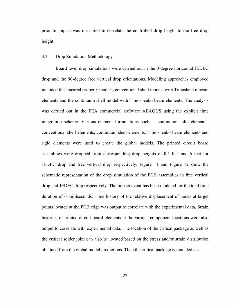
points were attached at various points on the edge of the board to facilitate the high speed
measurement of relative displacement (Figure 8). An image tracking software package
was used to quantitatively measure displacements during the drop event. The target point
at the top edge of the board was fixed as the reference and the relative displacements of
the other target points were calculated with respect to the reference. Significant effort was
put into ensuring a repeatable drop setup since small variations in the drop orientation
cause large variations in the dynamic response of the board. In case of free drop, the
inclination of the board with respect to a stationary vertical reference before and after
impact was measured to monitor the repeatability (Figure 10). The velocity of the board

24
Figure 5 PCB assembly subject to 90-degree free vertical drop.
Figure 6 PCB assembly subject to 0-degree JEDEC drop.
25
Figure 7 Measurement of initial angle prior to impact.
Figure 8 Test board with target points to measure relative displacement.

26
Figure 9 High Speed Image Analysis to Capture Displacement and Velocity.
Figure 10 Transient-Strain and Continuity for Determination of Component Failure.
27
prior to impact was measured to correlate the controlled drop height to the free drop
height.
3.2 Drop Simulation Methodology
Board level drop simulations were carried out in the 0-degree horizontal JEDEC
drop and the 90-degree free vertical drop orientations. Modeling approaches employed
included the smeared property models, conventional shell models with Timoshenko beam
elements and the continuum shell model with Timoshenko beam elements. The analysis
was carried out in the FEA commercial software ABAQUS using the explicit time
integration scheme. Various element formulations such as continuum solid elements,
conventional shell elements, continuum shell elements, Timoshenko beam elements and
rigid elements were used to create the global models. The printed circuit board
assemblies were dropped from corresponding drop heights of 0.5 feet and 6 feet for
JEDEC drop and free vertical drop respectively. Figure 11 and Figure 12 show the
schematic representation of the drop simulation of the PCB assemblies in free vertical
drop and JEDEC drop respectively. The impact event has been modeled for the total time
duration of 6 milliseconds. Time history of the relative displacement of nodes at target
points located at the PCB edge was output to correlate with the experimental data. Strain
histories of printed circuit board elements at the various component locations were also
output to correlate with experimental data. The location of the critical package as well as
the critical solder joint can also be located based on the stress and/or strain distribution
obtained from the global model predictions. Then the critical package is modeled as a

28
Figure 11 90-Degree Free Vertical Drop.
Figure 12 Zero-Degree Horizontal JEDEC Drop.

29
local model with a fine mesh to capture the detailed distribution of stresses and strains of
interconnects and the various individual layers.
3.3 Choice of Time Integration Formulation
The transient dynamic response of a printed circuit board under drop impact has
been investigated in the finite element domain with step-by-step direct integration in time
for both explicit and implicit formulations. Direct integration of the system is generally
used to study the nonlinear dynamic response of systems. The governing differential
equation of motion for a dynamic system can be expressed as,
[ ]{ } [ ]{ } { } { } ( )1intn
extRnRnDCnDM =++ &&&
For a linear problem, { } [ ]{ }nDKnR =int
where [M],[C] and [K] are the mass, damping and stiffness matrices respectively and
{ }nD is the nodal displacement vector at various instants of time.
Methods of direct integration calculate the dynamic response at time step n+1 from the
equation of motion, a central difference formulation and known conditions at one or more
preceding time steps. An explicit algorithm uses a difference expression of the general
form
{ } { } { } { } { }( ) ( )2....,1,,,1 −=+ nDnDnDnDfnD &&&
and is combined with the equation of motion at time step n.
An implicit algorithm uses a difference expression of the general form
{ } { } { } { } { } { }( ) ( )3....,,,,1,11 nDnDnDnDnDfnD &&&&&&++=+
and is combined with the equation of motion at time step n+1.

30
In case of the explicit method, the displacements and velocities are computed based on
quantities that are known at the beginning of each time step. All the terms on the right
hand side of Equation(2) are known and have already been calculated at earlier time steps
which is not the case for equation (3). It can be concluded that the solution of the
equation of motion in one time step is much simpler using the explicit algorithm as
compared to the implicit algorithm.
Explicit Formulation
For the explicit formulation,{ } 1+nD and { } 1−nD can be expanded using the Taylor
series to obtain:
{ } { } { } { } { } ( )
{ } { } { } { } { } ( )5nD6
3tnD
2
2tnDtnD1nD
4nD6
3tnD
2
2tnDtnD1nD
L&&&&&&
L&&&&&&
+Δ
−Δ
+Δ−=−
+Δ
+Δ
+Δ+=+
Subtracting Equation(5) from Equation(4) and neglected terms with orders of tΔ greater
than two, the velocity and acceleration at time step n can be approximated by the central
difference equations as :
{ } { } { }( ) ( )
{ } { } { } { }( ) ( )71nDnD21nD2t
11nD
61nD1nDt2
1nD
−+−+Δ
=−
−−+Δ=
&&
&
Substituting Equations (6) and (7) in the equation of motion, equation (1) written at time
step n and solving for{ } 1+nD , we get:

31
{ } { } { } [ ]{ } { }
( )8
121
21
22int
121
21
−⎥⎥⎦
⎤
⎢⎢⎣
⎡
Δ−
Δ−
Δ+−=+⎥
⎥⎦
⎤
⎢⎢⎣
⎡
Δ+
ΔnDC
tM
tnDM
tnRn
extRnDCt
Mt
Implicit Formulation
The equations for the displacement and velocity vectors at time step n+1 using the
Newmark relations can be expressed as:
{ } { } { } ( ){ }[ ] ( )
{ } { } { } { } ( ){ }[ ] ( )10nD211nD22t21
nDtnD1nD
9nD11nDtnD1nD
&&&&&
&&&&&&
ββ
γγ
−++Δ+Δ+=+
−++Δ+=+
where γ and β are numerical factors that control the characteristics of the algorithm,
such as accuracy, numerical stability and amount of algorithmic damping.
Solving equation (10) for { } 1+nD&& and substituting it into equation (9) we obtain the
following equation:
{ } { } { } { }( ) { } ( )
{ } { } { }( ) { } { } ( )12nD12
tnD1nD1nDt1nD
11nD121
nDtnD1nD2t
11nD
&&&&
&&&&&
⎟⎟⎠
⎞⎜⎜⎝
⎛−Δ−⎟⎟
⎠
⎞⎜⎜⎝
⎛−−−+Δ
=+
⎟⎟⎠
⎞⎜⎜⎝
⎛−−Δ−−+
Δ=+
βγ
βγ
βγ
ββ
Substituting equations (11) and (12) into the equation of motion, equation (1) written at
time step n+1 and solving for{ } 1+nD , we get :

32
{ } { } [ ] { } { } { }
[ ] { } { } { } ( )
[ ] [ ] [ ]KCt
M2t
1effK
where
13nD12
tnD1nDt
C
nD121
nDt
1nD
2t
1M1nextR1nDeffK
+ΔΔ
=⎥⎦⎤
⎢⎣⎡
⎭⎬⎫
⎩⎨⎧
⎟⎟⎠
⎞⎜⎜⎝
⎛−Δ+⎟⎟
⎠
⎞⎜⎜⎝
⎛−+
Δ+
⎪⎭
⎪⎬⎫
⎪⎩
⎪⎨⎧
⎟⎟⎠
⎞⎜⎜⎝
⎛−+
Δ+
Δ++=+⎥⎦
⎤⎢⎣⎡
βγ
β
βγ
βγ
βγ
βββ
&&
&&&
Considering the equation of motion for the explicit formulation, equation (8), if [M] is
made diagonal using the lumped approach, each time step is executed very quickly since
the solution of simultaneous equations is not required. It can also be shown that using the
lumped mass approach increases the allowable step time and provides better accuracy.
Also, the computer storage space required is reduced to a large extent. However, this
approach can be implemented only in the explicit formulation with great accuracy. For
the implicit formulation, considering equation (13), we can say that [ ]effK cannot be a
diagonal matrix since it contains [K]. As a result, the computational time required to
solve each time step is much higher as compared to explicit formulations. Therefore, a
diagonal mass matrix provides very little computational economy. Furthermore, the
implicit method is usually more accurate when [M] is the consistent mass matrix, thus
increasing the computational time and storage space. Explicit time integration
formulations are more suitable to solve wave propagation problems such as drop or
impact loading wherein the response of the system to the impact lasts only for a small
time interval. Implicit methods on the other hand are better suited to solve structural
dynamics problems where the response of the system needs to be analyzed for a longer

33
period of time. The explicit algorithm is conditionally stable i.e. there is a critical value
for the time step which must not be exceeded to avoid instability and error accumulation
in the time integration process. Element size in the explicit model has been limited due to
the conditional stability of the explicit time-integration, which influences the critical
value for the time step. This value of the critical step is given by:
( )
mode.maxωtheinratiodampingtheiswhereξ
1421max
2⎟⎠⎞
⎜⎝⎛ −−≤Δ ξξ
ωt
This limiting criterion increases the number of time steps required to span the time
duration of an analysis. The critical time step is also closely related to the time required
for a stress wave to cross the smallest element dimension in the model given by:
( )
modulus.elastictheisEanddensitytheis,lengthelementsticcharacteritheiswhere
15
ρ
ρ
lE
lt =Δ
As a result, a very finely meshed model can result in a higher time increment or if the
stress wave speed in the material is very high. This makes the method computationally
attractive for problems in which the total dynamic response time that must be modeled is
only a few orders of magnitude longer than the critical time step. Explicit time-
integration is well suited to wave propagation problems including drop impact, because
the dynamic response of the board decays within a few multiples of the longest period.
Most implicit formulations are unconditionally stable, which means that the process is
stable regardless of the size of the time step, thus allowing a fewer number of time steps
as compared to the explicit method. However, high deformation rates involved in impact,

34
using the implicit formulation with a large time step might introduce too much strain
increase in a single time-step, causing divergence in a large deformation analysis. A large
time-step may cause the contact force, which is proportional to the penetration of the
contact bodies, to be very large at the contact causing local distortion and failure.
Advantage of being able to use a larger time step with implicit methods can only be used
in a limited manner for impact analysis. The explicit formulation is better suited to
accommodate material and geometric non-linearity without any global matrix
manipulation. For these reasons, the explicit time integration formulation is used in this
analysis.
3.4 Element Formulations and Characteristics
Various modeling approaches have been employed to create the global and local
PCB assembly models. Three explicit model approaches have been investigated
including, smeared property models, Timoshenko beam element interconnect models
with continuum shell element, Timoshenko-beam element interconnect models with
conventional shell-element, and the explicit sub-models with a combination of
Timoshenko-beam elements and reduced integration hexahedral element corner
interconnects. The PCB in the global model has been modeled using reduced integration
shell elements (S4R) and continuum shell elements (SC8R). For each different type of
element used for the PCB, the various component layers such as the substrate, die attach,
silicon die and mold compound have been modeled with reduced integration solid
elements (C3D8R). Smeared properties have been derived for all the individual
components based on volumetric averaging and have been modeled using C3D8R

35
elements. The concrete floor has been modeled using rigid R3D4 elements. The solder
interconnections have been modeled with two-node Timoshenko beam elements (B31).
In the case of the local model, the PCB and the various layers of the package, namely the
substrate, die attach, silicon die, copper pad and mold compound have been modeled
using reduced integration solid elements (C3D8R). The four corner solder
interconnections were modeled using C3D8R elements while the remaining solder
interconnections are modeled using Timoshenko beam elements (B31). Table 2 and Table
3 show the element types used to model the various components in the global and local
models. Table 4 briefly summarizes the various element formulations used to create the
global models. Characteristics of these element types are discussed in detail in the
following literature.
1) Reduced Integration Solid (Continuum) Elements (C3D8R): General purpose solid
elements in ABAQUS can be used in linear and non-linear analyses involving contact,
plasticity and large deformations. Solid elements allow for finite strains and rotations in
large displacement analysis. C3D8R is a first order, eight node linear interpolation,
hexahedral element with reduced integration and hourglass control. It has three
translational degrees of freedom at each of its corner nodes. First order hexahedral solid
elements are generally preferred over first order triangular and tetrahedral elements in
stress analysis cases since the latter elements are extremely stiff and show slow
convergence with mesh refinement. Reduced integration schemes use a lower order
integration to form the element stiffness matrix, thus reducing the computational time
which is a significant consideration in dynamic analysis. First-order elements are
recommended when large strains or very high strain gradients are expected as in the case

36
of impact. They are better suited to tackling complex contact conditions and severe
element distortions. Higher order elements have higher frequencies than lower order
elements and tend to produce noise when stress waves move across an FE mesh.
Therefore, lower order elements are better than higher order elements at modeling a
shock wave front.
2) Timoshenko Beam Element (B31): Beam elements are one-dimensional
approximations of three-dimensional continuum based on the approximation that the
cross-sectional dimensions are small compared to the dimensions along the beam axis.
Timoshenko (shear flexible) beam elements (B31) available in ABAQUS are three-
dimensional beams in space. They use linear interpolation schemes and are useful in
dynamic problems such as impact. They have six degrees of freedom at each node
including, three translational degrees of freedom (1–3) and three rotational degrees of
freedom (4–6). The beam is modeled with a circular cross-section with an equivalent
radius so that it has the same mass as that of an actual solder interconnection. The rotary
inertia is calculated from the cross-sectional geometry. The Timoshenko beam elements
use a lumped mass formulation. The rotational degrees-of-freedom have been constrained
to model interconnect behavior. The B31 elements allow for shear deformation, i.e., the
cross-section may not necessarily remain normal to the beam axis. [Abaqus 2005b].
Shear deformation is useful for first-level interconnects, since it is anticipated that the
shear flexibility may be important. It is assumed throughout the simulation that, the
radius of curvature of the beam is large compared to distances in the cross-section and
that the beam cannot fold into a tight hinge.

37
Table 2 Components modeled in the global model and their respective element types.
Table 3 Components modeled in the local model and their respective element types.
Component Element Type
PCB S4R, SC8R
CSP C3D8R
Solder Interconnections B31
Rigid Floor R3D4
Attached Weight ( Free Drop ) C3D8R
Base and Screws (JEDEC Drop) C3D8R
Component Element Type
PCB C3D8R
CSP(Substrate, Silicon Die, Die Attach,
Mold Compound, Copper Pad) C3D8R
4 Corner Solder Interconnections C3D8R
Remaining Solder Interconnections B31

38
Table 4 Characteristics of element types used.
Element Type Number of
Nodes Characteristics
Degrees of
Freedom
C3D8R 8
First order, linear
interpolation, hexahedral
element with reduced
integration and hourglass
control.
Translational
(1,2,3)
S4R 4
Quadrilateral shell element,
linear interpolation with
reduced integration and a
large-strain formulation.
Translational
and
Rotational
(1,2,3,4,5,6)
SC8R 8
Hexahedral, first-order
interpolation, continuum
shell element with reduced
integration, finite membrane
strain
Translational
(1,2,3)
B31 2 Timoshenko beam, linear
interpolation formulation.
Translational
and
Rotational
(1,2,3,4,5,6)

39
It is also assumed that the strain in the beam's cross-section is the same in any direction in
the cross-section and throughout the section. For fine pitch solder interconnects, with
very low stand-off heights, the constant cross-section assumption is a fairly good
approximation. These elements are well suited for situations involving contact and
dynamic impact.
3) Shell Elements: Two types of shell elements are available in Abaqus™ including
conventional shell elements (S4R) and continuum shell elements (SC8R). The use of both
elements has been investigated for modeling transient-dynamic events.
a) Conventional Shell Elements (S4R): S4R is a quadrilateral shell element, linear
interpolation with reduced integration and a large-strain formulation. The conventional
shell elements discretize the surface by defining the element's planar dimensions, its
surface normal, and its initial curvature. Surface thickness is defined through section
properties. Shell elements are used for printed circuit board since, the thickness
dimension is significantly smaller than the other dimensions and the stresses in the
thickness direction are smaller than in the in-plane directions. The conventional shell-
element is a four-node reduced integration element which accounts for large strains and
large rotations. It has six degrees of freedom- 3 translational and 3 rotational degrees of
freedom per node.
b) Continuum Shell Elements (SC8R):SC8R is a hexahedral, first-order interpolation,
continuum shell element with reduced integration. Continuum shell elements (SC8R)
resemble three-dimensional solid elements and discretize the entire three-dimensional
body. The continuum shell elements are formulated such that their kinematic and
constitutive behavior is similar to conventional shell elements. The continuum shell

40
element (SC8R) has three-translational degrees of freedom at each node and the element
accounts for finite membrane strains and arbitrarily large rotations [Abaqus 2005a].
Continuum shell elements provide a refined response through the thickness and are more
accurate in modeling contact than conventional shell elements.
Solid (Continuum) Elements Continuum Shell Elements
Conventional Shell Elements Timoshenko Beam Element
Figure 13 Various element formulations employed to create the explicit models.

41
CHAPTER 4
FINITE ELEMENT MODELS FOR DROP SIMULATION
Various finite element models were developed to predict the transient dynamic
behavior of printed circuit board assemblies subject to drop in the 90-degree free vertical
direction and the horizontal direction in accordance with the JEDEC standard, JESD22-
B11. Models developed to simulate free and JEDEC drop included smeared property
models, conventional shell elements with Timoshenko beam elements and continuum
shell elements with Timoshenko beam elements. The board-level assembly consisted of
10 components mounted on the printed circuit board. Figure 14 shows the typical
architecture for the tape array ball grid array (TABGA) packages investigated in this
study. Figure 15 and Figure 16 shows the schematic for the 90-degree free vertical drop
and zero-degree horizontal JEDEC simulation of the TABGA board. The linear elastic
material properties for the various individual layers of the package are listed in Table 5.
4.1 Smeared Property Global Model
The smeared property approach is based on the principle of volumetric averaging.
This approach was proposed by Clech [1996, 1998] for the development of closed form
models for solder joints subjected to thermal fatigue. In this method, the various
individual layers of the chip scale package (CSP) namely the substrate, die attach, silicon

42
Figure 14 Typical architecture for TABGA package.

43
Figure 15 Schematic of 90-Degree Free Vertical Drop.
Figure 16 Schematic of Zero-Degree JEDEC Drop.

44
Table 5 Material Properties for individual layers of TABGA package.
Component
Elastic Modulus,
E
(Pa)
Poisson’s Ratio
(ν)
Density, ρ
(kg/m3)
Printed Circuit Board 1.6e9 0.33 1730
Solder(63Sn/37Pb) 3.2e10 0.38 8400
Silicon Die 1.124e11 0.28 2329
Copper Pad 1.29e11 0.34 8900
Die Attach 2.758e9 0.35 2200
Substrate 2.4132e10 0.30 1400
Mold Compound 1.5513e10 0.25 1970

45
die, mold compound and the solder interconnections are represented by a homogeneous
block of elements such that it has the equivalent mass as that of the original package. The
printed circuit board is modeled using first order reduced integration conventional shell
elements (S4R) while the smeared property elements are modeled using first order
reduced integration continuum solid elements (C3D8R). In case of free drop, the weight
attached at the top edge of the board is also modeled using C3D8R elements. In case of
JEDEC drop, the connecting screws and the steel base are modeled using C3D8R
elements. The impacting concrete floor was modeled with R3D4 elements. Figure 17
shows the components modeled using smeared property elements. Table 6 summarizes
the various element formulations employed to create the components of the smeared
model. In order to ensure that the CSP represented by smeared elements closely
represents the actual component, it is necessary to accurately calculate the equivalent
material properties of the smeared elements. The method to obtain these parameters is
explained below. Table 7 shows the masses, volumes and the equivalent layer thicknesses
of the various layers considered for the calculation of the smeared properties. The
equivalent thickness of each individual layer is calculated by considering each layer to
have an 8mm square cross-section which is the size of each individual component.
The nomenclature used in the equations used below is as follows:
..
..
.'.'
componentsindividualofVolumevcomponentsindividualofModulusElasticE
elementsmearedofModulusElasticEcomponentsindividualofThicknessLayerh
componentsindividualofRatiosPoissonelementsmearedofRatiosPoisson
k
k
c
k
k
c
−−−−−−
υυ

46
Figure 17 PCB modeled using shell (S4R) elements and CSP using smeared properties.

47
Table 6 Element types used in smeared property models.
Table 7 Dimensions and masses of individual layers in the package. Component Volume (m3) Mass(kg) Equivalent Layer
Thickness (m)
Solder 2.105e-9 1.769e-5 3.2891e-5
Die Attach 1.875e-9 4.125e-6 2.9297e-5
Silicon Die 7.250e-9 1.689e-5 1.132e-4
Mold Compound 6.019e-8 1.186e-4 9.4047e-4
Substrate 6.015e-8 8.421e-6 9.398e-5
Table 8 Comparison of Actual and Simulated Component Masses using Smeared
Property Models.
Component Actual (gm) Smeared Model (gm)
PCB 28.15 28.65
8 mm CSP 0.14 0.142
Weight 31.8 31.8
Component Element Type
PCB S4R
CSP (Smeared Elements) C3D8R
Rigid Floor R3D4

48
Calculation of Equivalent Poisson’s Ratio
2626.0
31020984.1
4101776.3
510398.94104047.9510132.15109297.25102891.3
)510398.93.0(
)4104047.925.0()410132.128.0()5109297.235.0()5102891.338.0(
1
1
=
−×
−×=
−×+−×+−×+−×+−×
−××
+−××+−××+−××+−××
=
∑=
∑==
c
c
c
n
kkh
n
kkhk
c
υ
υ
υ
υυ
Calculation of Equivalent Elastic Modulus
2/9102725.7
)3.01(12
3)510398.9(10104132.2)25.01(12
3)4104047.9(10105513.1)28.01(12
3)410132.1(1110124.1
)35.01(12
3)5109297.2(910758.2)38.01(12
3)5102891.3(10102.3)2626.01(12
3)31020984.1(
1 )1(12
3
)1(12
3
mNcE
cE
n
k kkhkE
cchcE
×=
−
−×××+
−
−×××+
−
−×××
+−
−×××+
−
−×××=
−
−××
∑= −
=− υυ
Calculation of Equivalent Density
3/2140
910015.6810019.6910250.7910875.1910105.2
)910015.61400(
)810019.61970()910250.72329()910875.12200()910105.28400(
1
1
mkgc
c
n
kkv
n
kkvk
c
=
−×+−×+−×+−×+−×
−××+
−××+−××+−××+−××
=
∑=
∑==
ρ
ρ
ρ
ρ

49
Table 8 shows the simulated weight of the smeared property model for all components
and the test board and the actual weights. It can be seen that the simulated weight of the
PCB assembly closely approximates the actual weight. The printed circuit board
assemblies were dropped from a height of 6 feet in the vertical orientation for free drop
and from a height of 0.5 feet in the horizontal orientation for JEDEC drop. To save
computational time, the near-impact velocity of the test assembly, which is a function of
drop height, is applied as an initial condition to the various components of the PCB
assembly. The relation is given by:
gHV 2=
where V is the impact velocity corresponding to drop height H.
For free drop, the initial velocity corresponding to a height of 6 feet i.e. 1.8288 meters is
given by:
.s/m992.5V
8288.181.92V
=
××=
For JEDEC drop, the initial velocity corresponding to a height of 0.5 feet i.e. 0.1524
meters is given by:
.s/m729.1V
1524.081.92V
=
××=
A weight was attached at the top edge of the board to control the drop orientation. A
reference node was placed behind the rigid floor for application of constraints and all the
degrees of freedom of that node were constrained. Node to surface contact was specified
between the impacting edge of the PCB and the rigid floor for free drop simulation. Node

50
to surface contact was specified between the impacting bottom surface of the steel base
and the rigid floor for JEDEC drop. The impact event was modeled for the total time
duration of 6 milliseconds. Time history of the relative displacements of nodes at target
points located at the PCB edge were output to correlate with the experimental data. Strain
histories of printed circuit board elements at all the component locations were also output
to correlate with experimental data.
Figure 18 shows the correlation between the predicted transient mode shapes of the PCB
assembly and the experimental mode shapes which were obtained by recording the actual
drop event using high-speed cameras at time intervals of 2.4 ms and 4.5 ms for free drop.
Figure 19 shows the correlation between the predicted transient mode shapes of the PCB
assembly and the experimental mode shapes which were obtained by recording the actual
drop event using high-speed cameras at time intervals of 2.4 ms and 4.8 ms for JEDEC
drop. Good correlation has been achieved between the predicted and experimentally
observed mode shapes. Correlation of peak relative displacements and strains with
experimental data is discussed later in this chapter.
4.2 Conventional Shell-Beam Model
In this approach, the PCB has been modeled using first-order reduced integration four-
node conventional shell elements (S4R) and each solder interconnection is represented by
three-dimensional Timoshenko beams in space (B31) with six degrees of freedom. S4R is
a quadrilateral shell element, linear interpolation with reduced integration and a large-
strain formulation. Shell elements are used for printed circuit board since the thickness
dimension is significantly smaller than the other dimensions. Beam elements are one-

51
t = 2.4 ms
t = 4.5 ms
t = 2.4 ms
t = 4.5 ms
Figure 18 Correlation of Transient Mode-Shapes for Smeared Element Model during Free Vertical Drop.

52
t = 2.4 ms
t = 4.8 ms
t = 2.4 ms
t = 4.8 ms
Figure 19 Correlation of Transient Mode-Shapes for Smeared Element Model during JEDEC Drop.

53
dimensional approximations of three-dimensional continuum based on the approximation
that the cross-sectional dimensions are small compared to the dimensions along the beam
axis. The beam is modeled with a circular cross-section with an equivalent radius so that
it has the same mass and volume as that of an actual solder interconnection. The
dimensions of the solder joint were measured by observing a cross-sectional sample of
the package under an electron microscope. Using those dimensions, the solder joint was
modeled as a linear elastic material and its volume and mass were calculated. The
Timoshenko beam was then given an equivalent radius to define its cross-section such
that it had the same mass and volume as that of the original solder joint as shown below:
mr
hr
hr
m
m
4105933.1
11-101.5952 Therefore,
2 beamsolder single of Volume
:have wein volume, lcylindrica be tobeam thegConsiderin
3-10 0.2 (h)joint solder ofHeight
311-101.595joint solder single of Volume
−×=⇒
=
=
×=
=
π
π
All the individual layers of the package such as the substrate, die attach, silicon die and
the mold compound have been modeled in detail using first order reduced integration
continuum solid elements (C3D8R). The weight attached at the top edge of the board is
also modeled using C3D8R elements. The impacting concrete floor was modeled with
R3D4 elements. The connecting screws and the steel base were modeled using solid
elements (C3D8R). Element types to model the various components of the models are
listed in Table 9. Table 10 shows the simulated weight of the various components of the
conventional shell-beam model and the actual weights. It can be seen that the simulated
weight of the PCB assembly closely approximates the actual weight. The impacting

54
Figure 20 Solder Interconnection Layout Modeled Using Timoshenko Beam elements.
Figure 21 Printed-Circuit Assembly with Timoshenko-Beam Element Interconnects and Conventional Shell-Elements.

55
Table 9 Element types used in Conventional Shell-Beam model.
Table 10 Comparison of Actual and Simulated Component Masses using Conventional
Shell-Beam Model.
Component Actual (gm) Smeared Model (gm)
PCB 28.15 28.65
8 mm CSP 0.14 0.148
Weight 31.8 31.8
Component Element Type
PCB S4R
Solder Interconnections B31
Substrate C3D8R
Silicon Die C3D8R
Die Attach C3D8R
Mold Compound C3D8R
Rigid Floor R3D4
56
concrete floor was modeled with R3D4 elements. Figure 20 shows the layout of the
solder interconnections modeled using the Timoshenko beam elements. Figure 21 shows
the close-up of one of the packages with the PCB modeled using S4R elements and its
cross-sectional view with all the individual layers. Drop simulation of the PCB assembly
was carried out from a height of 6 feet in the vertical orientation for free drop and a
height of 0.5 feet in the horizontal orientation. To save computational time, initial
velocities of 5.992 m/s and 1.729 m/s corresponding to heights of 6 feet and 0.5 feet were
applied to the nodes of all the components in the assembly for free vertical drop and
JEDEC drop respectively. The rotational degrees of freedom of the Timoshenko beam
elements were constrained to model interconnect behavior. Node to surface contact was
specified between the impacting edge of the PCB and the reference node of the rigid floor
for free drop simulation. Similarly, node to surface contact was specified between the
impacting surface of the base and the reference node of the rigid floor which was
constrained in all degrees of freedom for JEDEC drop. The impact event was modeled for
the total time duration of 6 milliseconds. Time history of the relative displacement of
nodes at target points located at the PCB edge and the PCB strain histories at various
component locations were output to correlate with the experimental data.
Figure 22 shows the correlation between the predicted transient mode shapes of
the PCB assembly and the experimental mode shapes which were obtained by recording
the actual drop event using high-speed cameras at time intervals of 2.4 ms and 4.2 ms for
free drop. Figure 23 shows the correlation between the predicted transient mode shapes of
the PCB assembly and the experimental mode shapes which were obtained by recording
the actual drop event using high-speed cameras at time intervals of 2.4 ms and 4.8 ms in

57
case of JEDEC drop. Good correlation has been achieved between the predicted and
experimentally observed mode shapes. Correlation of peak relative displacements and
strains with experimental data has been discussed later in this chapter.
4.3 Continuum Shell-Beam Model
In this approach, the PCB has been modeled using first-order reduced integration eight-
node continuum shell elements (SC8R) and each solder interconnection is represented by
three-dimensional Timoshenko beams in space (B31) with six degrees of freedom. SC8R
is a hexahedral, first-order interpolation, continuum shell element with reduced
integration. Continuum shell elements (SC8R) resemble three-dimensional solid elements
and discretize the entire three-dimensional body. Beam elements are modeled with a
circular cross-section with an equivalent radius so that it has the same mass and volume
as that of an actual solder interconnection as shown below:
mr
hr
hr
m
m
4105933.1
11-101.5952 Therefore,
2 beamsolder single of Volume
:have wein volume, lcylindrica be tobeam thegConsiderin
3-10 0.2 (h)joint solder ofHeight
311-101.595joint solder single of Volume
−×=⇒
=
=
×=
=
π
π
All the individual layers of the package such as the substrate, die attach, silicon die and
the mold compound have been modeled in detail using first order reduced integration
continuum solid elements (C3D8R). The impacting concrete floor was modeled with
R3D4 elements.

58
t = 2.4 ms
t = 4.2 ms
t = 2.4 ms
t = 4.2 ms
Figure 22 Correlation of Transient Mode-Shapes for Conventional-Shell Timoshenko-
Beam Model during Free Vertical Drop.

59
t = 2.4 ms
t = 4.8 ms
t = 2.4 ms
t = 4.8 ms
Figure 23 Correlation of Transient Mode-Shapes for Conventional-Shell Timoshenko-
Beam Model during JEDEC Drop.

60
Element types to model the various components of the models are listed in Table 11.
Table 12 shows the simulated weight of the various components of the continuum shell-
beam model and the actual weights. It can be seen that the simulated weight of the PCB
assembly closely approximates the actual weight. Figure 24 shows the layout of the
solder interconnections modeled using the Timoshenko beam elements. Figure 25 shows
the close-up of one of the packages with the PCB modeled using SC8R elements and its
cross-sectional view with all the individual layers. Drop simulation of the PCB assembly
was carried out from a height of 6 feet in the vertical orientation for free drop and a
height of 0.5 feet in the horizontal orientation. To save computational time, initial
velocities of 5.992 m/s and 1.729 m/s corresponding to heights of 6 feet and 0.5 feet were
applied to the nodes of all the components in the assembly for free vertical drop and
JEDEC drop respectively. The rotational degrees of freedom of the Timoshenko beam
elements were constrained to model interconnect behavior. Node to surface contact was
specified between the impacting edge of the PCB and the reference node of the rigid floor
for free drop simulation. Similarly, node to surface contact was specified between the
impacting surface of the base and the reference node of the rigid floor which was
constrained in all degrees of freedom for the JEDEC drop. The impact event was
modeled for the total time duration of 6 milliseconds. Time history of the relative
displacement of nodes at target points located at the PCB edge and the PCB strain
histories at various component locations were output to correlate with the experimental
data. Figure 26 shows the correlation between the predicted transient mode shapes of the
PCB assembly and the experimental mode shapes which were obtained by recording the

61
Table 11 Element types used in Continuum Shell-Beam model.
Table 12 Comparison of Actual and Simulated Component Masses using Continuum
Shell-Beam Model.
Component Actual (gm) Smeared Model (gm)
PCB 28.15 28.65
8 mm CSP 0.14 0.148
Weight (Free Drop) 31.8 31.8
Component Element Type
PCB SC8R
Solder Interconnections B31
Substrate C3D8R
Silicon Die C3D8R
Die Attach C3D8R
Mold Compound C3D8R
Rigid Floor R3D4
Attached Weight (Free Drop) C3D8R
Connecting Screws (JEDEC Drop) C3D8R
Steel Base (JEDEC Drop) C3D8R

62
Figure 24 Solder Interconnection Layout Modeled Using Timoshenko Beam elements.
AA’
Section AA’
Chip Die-AttachSubstrate
SolderInterconnects
Mold Compound
AA’
Section AA’
AA’
Section AA’
Chip Die-AttachSubstrate
SolderInterconnects
Mold Compound
Figure 25 Printed-Circuit Assembly with Timoshenko-Beam Element Interconnects and
Continuum Shell-Elements.

63
t = 2.4 ms
t = 4.5 ms
t = 2.4 ms
t = 4.5 ms
Figure 26 Correlation of Transient Mode-Shapes for Continuum-Shell Timoshenko-
Beam Model during Free Vertical Drop.

64
t = 2.4 ms
t = 4.8 ms
t = 2.4 ms
t = 4.8 ms Figure 27 Correlation of Transient Mode-Shapes for Continuum-Shell Timoshenko-
Beam Model during JEDEC Drop.

65
actual drop event using high-speed cameras at time intervals of 2.4 ms and 4.5 ms for free
drop. Figure 27 shows the correlation between the predicted transient mode shapes of the
PCB assembly and the experimental mode shapes which were obtained by recording the
actual drop event using high-speed cameras at time intervals of 2.4 ms and 4.8 ms for
JEDEC drop. Good correlation has been achieved between the predicted and
experimentally observed mode shapes.
4.4 Correlation of Predicted Peak Relative Displacement and Strain Histories
In this section, the field quantities and derivatives of field quantities namely relative
displacement and strain from both various explicit finite element models and
experimental data have been compared for both free drop and JEDEC drop. Specifically,
peak relative displacement and peak strain values have been correlated for the models
versus experimental data. The peak strain values exhibit error in the range of 10-30 % as
observed in Table 13. All the three modeling approaches including smeared properties,
conventional-shell with beam elements, and continuum-shell with beam elements exhibit
similar results. The peak relative displacement values as shown in Table 14 exhibit error
in the neighborhood of 8-28%. Table 15 and Table 16 list the computational efficiency
versus number of elements and nodes for all the global models for free and JEDEC drop
respectively. Figure 28 and Figure 29 show the correlation of the board relative
displacement 2.4 ms and 4.5 ms after impact, from high-speed image analysis with the
model predictions from smeared, continuum-shell with Timoshenko-beam, conventional-
shell with Timoshenko-beam models for JEDEC drop and free drop respectively.

66
Table 13 Correlation of Peak-Strain Values from Model Predictions Versus Experiments
for 90-degree Free-Drop.
Loc 1 Loc 3 Loc 5
Experiment 1417 2248 1667
Smeared Property 1603 1563 1424
Error (%) -13.15 30.48 14.56
Timoshenko-Beam with
Continuum Shell 1820 1990 1960
Error (%) -28.47 11.49 -17.60
Timoshenko-Beam with
Conventional Shell 1760 1630 2070
Error (%) -24.24 27.50 -24.20

67
Table 14 Correlation of peak relative displacement values between various explicit
models.
Loc 1 Loc 3 Loc 5
Experiment (mm) 3.61 4.47 4.58
Smeared Property 3.86 3.35 3.39
Error (%) -7.03 24.93 25.86
Timoshenko-Beam, Continuum
Shell 3.80 4.16 3.26
Error (%) -5.17 6.97 28.73
Timoshenko-Beam,
Conventional Shell 4.43 4.85 4.15
Error (%) -22.8 -8.62 9.21

68
Table 15 Computational efficiency for various explicit models subject to free drop.
Model Number of
elements
Number of
nodes
Computational
time(sec)
Smeared Model 75809 79126 59400
Conventional Shell-Beam
Model 118089 133576 219600
Continuum Shell-Beam
Model 214857 264124 568800
Table 16 Computational efficiency for various explicit models subject to JEDEC drop.
Model Number of
elements
Number of
nodes
Computational
time
Smeared Model 77825 82135 43200
Conventional Shell-Beam
Model 120105 136585 226800
Continuum Shell-Beam
Model 218026 268480 584580

69
-0.0075
-0.0055
-0.0035
-0.0015
0.0005
0.0025
0.0045
0.0065
0 50 100 150 200
Board Length (mm)
Rel
ativ
e D
ispl
acem
ent (
met
er)
Smeared Model Conventional Shell-Beam Model
Continuum Shell-Beam Model Experimental Data
Figure 28 Correlation Between Experimental Relative Displacement of Board Assembly
at 2.4 ms with Model Predictions under zero-degree JEDEC drop-test.
-0.05-0.045
-0.04-0.035
-0.03-0.025
-0.02-0.015
-0.01-0.005
0
0 20 40 60 80 100 120 140 160
Board Length (mm)
Rel
ativ
e D
ispl
acem
ent (
met
er)
Smeared model Conventional Shell-Beam Model
Continuum Shell-Beam Model Experimental data
Figure 29 Correlation Between Experimental Relative Displacement of Board Assembly
at 4.5 ms with Model Predictions under 900 free drop-test.

70
4.5 Error estimation in incorporating symmetry based models
When any electronic product is subject to drop impact, the orientation in which it
may strike the impacting surface varies with each scenario. The use of symmetry-based
models to represent this free drop would not account for the primary critical anti-
symmetric mode shapes that dominate during impact. In case of the free vertical drop and
the JEDEC drop simulations modeled in this paper, the stress and strain distributions
experienced by the various solder interconnections in any package is not symmetrical.
Figure 30 shows the variations in the stress distribution in the array of solder
interconnections in the conventional shell-beam model subject to a JEDEC drop. If a
diagonal slice model was used considering only the solder joints above Section AA based
on the symmetry boundary conditions, the stresses in the top left and bottom right solder
interconnections would be considered equal which is not true. This would result in an
error of around 121% in the predicted value of the stress as shown in Table 17. Table 18
shows an error of about 107% in predicting the stresses in the solder interconnection in
the continuum shell-beam model subject to free drop while incorporating a half symmetry
model. The magnitude of errors clearly suggests that the use of diagonal slice models and
half symmetry models for modeling drop simulations would be an inaccurate
representation of the actual drop event.
4.6 Solder Interconnect Strain Histories in the Global Model
The strain distribution in the solder interconnections in both the conventional
shell-Timoshenko beam model and the continuum shell-Timoshenko beam model for
both free and JEDEC drop varies with the location of the interconnects in the assembly.

71
A
A
A
A
Figure 30 Stress distribution in the Timoshenko-beam solder interconnects subject to
JEDEC drop for the conventional shell-beam model.
Table 17 Estimated error in prediction of solder interconnect stress in using diagonal
symmetry model for conventional shell beam model subject to JEDEC Drop.
Model Prediction Von Mises Stress (Pa) in Solder Interconnect Error (%)
Full Model 710 1.887×
Diagonal Symmetry Model 710 4.175×
-121.25
Table 18 Estimated error in prediction of solder interconnect stress in using half
symmetry model for continuum shell-beam model subject to Free Drop.
Model Prediction Von Mises Stress (Pa) in Solder Interconnect Error (%)
Full Model 710 1.66098×
Half Symmetry Model 710 3.438×
-107

72
Figure 32 and Figure 33 show the strain plots from the Timoshenko-Beam Element with
Conventional-Shell model prediction for the solder interconnection located at the
outermost corner of the package and in the solder interconnect located at the corner of the
fourth-row from the outside, during a 90° free vertical drop.
Plots indicate that the transient strain history is very different at the four-corners of the
chip-scale package. Therefore, the susceptibility of the solder interconnects to failure
may be different in different corners. A comparison of transient strain histories in the
solder interconnections at the corner of the package and the die shadow region reveals
that, a large portion of the strain is carried by the outside row of the solder interconnects.
This phenomenon can be observed at all the component locations for both conventional
shell-Timoshenko beam model and the continuum shell-Timoshenko beam model for
both free and JEDEC drops.
4.7 Explicit Sub-model for Drop Simulation
Sub-modeling can be described as a technique to study a local part of a model with a
refined mesh based on interpolation of the solution of a relatively coarse, global model. It
is generally used to obtain an accurate, detailed solution of a local region. Employing the
sub-modeling technique includes running the global model and saving the results in the
vicinity of the location of the sub-model boundary. The results from the global model are
then interpolated onto the nodes on the appropriate parts of the boundary of the sub-
model. The sub-model is then analyzed based on the solution of the global model to
obtain the detailed response of the local region.

73
Top Left
Bottom RightBottom Left
Top RightTop Left
Bottom RightBottom Left
Top Right
Figure 31 Representation of solder interconnection array.
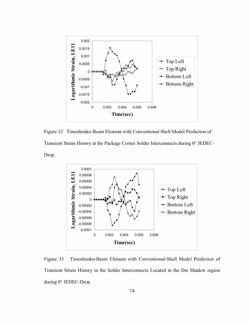
74
-0.002
-0.0015
-0.001
-0.0005
0
0.0005
0.001
0.0015
0.002
0 0.002 0.004 0.006 0.008
Time(sec)
Log
arith
mic
Str
ain,
LE
11
Top LeftTop RightBottom LeftBottom Right
Figure 32 Timoshenko-Beam Element with Conventional-Shell Model Prediction of
Transient Strain History at the Package Corner Solder Interconnects during 0° JEDEC-
Drop.
-0.0001
-0.00008
-0.00006
-0.00004
-0.00002
0
0.00002
0.00004
0.00006
0.00008
0.0001
0 0.002 0.004 0.006 0.008
Time(sec)
Log
arith
mic
Str
ain,
LE
11
Top LeftTop RightBottom LeftBottom Right
Figure 33 Timoshenko-Beam Element with Conventional-Shell Model Prediction of
Transient Strain History in the Solder Interconnects Located in the Die Shadow region
during 0° JEDEC-Drop.

75
The printed circuit board assembly consists of various layers such as the copper
pad, solder interconnections, solder mask, silicon die etc. with multiple scale differences
in their dimensions. Studying the stress/strain variations in the solder interconnections for
failure prediction while at the same time capturing the dynamic response of the assembly
would result in a very finely meshed model thereby increasing the computational time.
To overcome these difficulties and achieve computational efficiency with reasonable
accuracy, a global local or sub-modeling technique is employed to study the local critical
part of the model with a refined mesh based on interpolation of the solution from an
initial, relatively coarse global model. The advantage of this technique is that both the
global and local models can be maintained sufficiently small in size thus requiring less
computational time with reasonable accuracy. The sub-model consists of a detailed model
located at the position of the critical package which is determined by the solution of the
global model. It consists of the part of the printed circuit board modeled using first order
reduced integration continuum solid elements (C3D8R), the individual layers of the
package namely the copper pads, die attach, silicon die, substrate and the mold compound
modeled using C3D8R elements and the solder interconnections modeled using a
combination of Timoshenko beam elements (B31) and solid elements (C3D8R). The four
corner solder interconnections, being the most critical, are modeled using the hexahedral
solid elements (C3D8R) in order to obtain the detailed response in terms of stresses and
strains for these interconnections. The remaining solder interconnections are modeled
using the Timoshenko beam elements. Table 19 shows the various element formulations
employed to model the explicit sub-model. Figure 34 shows the solder interconnection
layout in the explicit sub-model with a combination of hexahedral-element corner

76
interconnects and Timoshenko-beam element interconnects. Figure 35 shows the cross-
section of the explicit sub-model with the various individual layers such as the PCB,
substrate, copper pad etc. Initial velocities are assigned to all the nodes of the various
components of the local model. The location of the critical package as well as the critical
solder joint can also be located based on the stress and/or strain distribution obtained
from the global model prediction. Then the critical package is modeled as a local model
with a fine mesh to capture the detailed distribution of stresses and strains of
interconnects and the various individual layers.
4.8 Solder Interconnect Strain Histories in the Local Model
The global beam-shell model predictions indicate that a large portion of the strain is
carried by the outside row of the solder interconnects. Therefore, the four corner solder
interconnections, being the most critical, are modeled using the hexahedral solid elements
(C3D8R) in order to obtain the detailed response in terms of stresses and strains for these
interconnections. The remaining solder interconnections are modeled using the
Timoshenko beam elements. Figure 36 and Figure 37 show the strain distributions in the
solder joints in the local model at various time intervals. These local models were
analyzed based on the global responses of the Conventional Shell-Timoshenko beam
model subject to JEDEC drop and free vertical drop respectively. Both figures show that
the strain distributions in the solder interconnections are not equal or symmetrical
justifying the use of the full models.

77
Table 19 Element types used in the explicit sub-model.
Figure 34 Solder Interconnection Layout in Explicit Sub-model with a combination
Hexahedral-Element Corner Interconnects and Timoshenko-Beam Element
Interconnects.
Component Element Type
PCB C3D8R
Four Corner Solder Interconnections C3D8R
Remaining Solder Interconnections B31
Substrate C3D8R
Copper Pad C3D8R
Silicon Die C3D8R
Die Attach C3D8R
Mold Compound C3D8R

78
Figure 35 Local Explicit Sub-Model with Hexahedral-Element Corner Interconnects,
Timoshenko-Beam Element Interconnects and PCB meshed with Hexahedral Reduced
Integration-Elements.

79
The hexahedral element mesh solder interconnects provide insight into the logarithmic
strain distributions in the solder interconnects. Figure 38 and Figure 39 show the explicit
sub-model predictions of transient logarithmic shear strains, LE12 and LE23, in the
solder interconnect of one of the chip-scale packages on the printed circuit board
assembly corresponding to the Conventional Shell-Timoshenko Beam global model
subject to JEDEC drop. Figure 40 and Figure 41 show the explicit sub-model predictions
of transient logarithmic shear strains, LE12 and LE23, in the solder interconnect of one of
the chip-scale packages on the printed circuit board assembly corresponding to the
Continuum Shell-Timoshenko Beam global model subject to free drop. Model results
indicate that the strains are maximum at the solder-joint to package interface and the
solder-joint to printed circuit board interface, indicating a high probability of failure at
these interfaces. Figure 42 shows the cross-section of corner solder interconnects in the
failed samples showing higher susceptibility of the samples to fail at the package-to-
solder interconnect interface or the solder-to-printed circuit board interface. Failure
analysis of the samples reveals that the observed failure modes correlate will with the
model predictions. Interface failure is generally observed in dynamic events such as drop
impact due to the high strain rates experienced by the solder joints. The strength of the
bulk solder increases with strain rate while that of the inter-metallic compounds decreases
with strain rate. As a result, large stresses are developed at the solder joint interface
leading to eventual failure.

80
t = 2.4 ms t = 3.6 ms
t = 4.8 ms t = 6 ms
t = 2.4 ms t = 3.6 ms
t = 4.8 ms t = 6 ms
Figure 36 Strain histories in the local model corresponding to Conventional Shell
Timoshenko-beam global model during JEDEC-drop at various time intervals.

81
t = 2.4 ms t = 3.6 ms
t = 4.8 ms t = 6 ms
t = 2.4 ms t = 3.6 ms
t = 4.8 ms t = 6 ms
Figure 37 Strain histories in the local model corresponding to Conventional Shell
Timoshenko-beam global model during free vertical drop at various time intervals.

82
t = 2.4 ms t = 3.6 ms
t = 4.8 ms t = 6 ms
t = 2.4 ms t = 3.6 ms
t = 4.8 ms t = 6 ms
Figure 38 Global-Local Explicit Sub-Model Predictions of Transient Logarithmic Shear
Strain, LE12, in the Solder Interconnect of one of the Chip-Scale Packages on the Printed
Circuit Board Assembly during JEDEC Drop.

83
t = 2.4 ms t = 3.6 ms
t = 4.8 ms t = 6 ms
t = 2.4 ms t = 3.6 ms
t = 4.8 ms t = 6 ms
Figure 39 Global-Local Explicit Sub-Model Predictions of Transient Logarithmic Shear
Strain, LE23, in the Solder Interconnect of one of the Chip-Scale Packages on the Printed
Circuit Board Assembly during JEDEC Drop.

84
t = 2.4 ms t = 3.6 ms
t = 4.8 ms t = 6 ms
t = 2.4 ms t = 3.6 ms
t = 4.8 ms t = 6 ms
Figure 40 Global-Local Explicit Sub-Model Predictions of Transient Logarithmic Shear
Strain, LE12, in the Solder Interconnect of one of the Chip-Scale Packages on the Printed
Circuit Board Assembly during Free Drop.

85
t = 2.4 ms t = 3.6 ms
t = 4.8 ms t = 6 ms
t = 2.4 ms t = 3.6 ms
t = 4.8 ms t = 6 ms
Figure 41 Global-Local Explicit Sub-Model Predictions of Transient Logarithmic Shear
Strain, LE23, in the Solder Interconnect of one of the Chip-Scale Packages on the Printed
Circuit Board Assembly during Free Drop.

86
Figure 42 Cross-section of corner solder interconnect in the failed samples showing
higher susceptibility of the samples to fail at the package-to-solder interconnect interface
or the solder-to-printed circuit board interface.

87
4.9 Susceptibility to Chip Fracture
Figure 43 shows the contour plot of the stress, S33 in the silicon chip located in one of
the components of the Conventional Shell-Timoshenko beam model subject to JEDEC
drop at various time intervals. Figure 44 shows the transient stress history on the chip
bottom-surface for chip-scale packages at two-locations on the test board. The stress, S33
varies in the range of 10 MPa. This is significantly smaller than the fracture stress of
7GPa published for silicon in [Petersen 1982, Pourahmadi et al. 1991], indicating a
significant design margin of safety for chip-fracture during drop. In reality, the design
margin can be reduced dramatically because of chip-surface imperfections.

88
t = 2.4 ms t = 3.6 ms
t = 5.1 ms t = 5.7 ms
t = 2.4 ms t = 3.6 ms
t = 5.1 ms t = 5.7 ms
Figure 43 Transient stress history in the silicon chip.
-15
-10
-5
0
5
10
15
0 0.002 0.004 0.006 0.008
Time(Secs)
Stre
ss, S
33 (M
Pa)
Chip BottomSurfaceChip TopSurface
Figure 44 Transient Stress History in Chip Top and Bottom Surfaces.

89
CHAPTER 5
FAILURE PREDICTION MODELS
5.1 Overview
Brittle interfacial fracture failure at the solder joint-copper pad interface is
commonly observed in first level solder interconnects of electronic products subject to
high strain rates as in the case of impact loading. It has been observed that the fracture
strength of the ductile bulk solder increases with increase in strain rate while that of the
brittle inter-metallic compound (IMC) decreases with increase in strain rate. Two
modeling approaches have been developed to investigate the failure mechanisms in the
solder interconnections under drop impact namely the Timoshenko-Beam failure model
and the cohesive zone modeling.
Figure 45 Brittle interfacial failure observed in the solder interconnections at the
package side and the PCB side.

90
Tensile testing of solder joint arrays was carried out to study the interfacial failures in
solder joints [Darveaux et al. 2006] on a mechanical testing machine as shown in Figure
46. Strain rates used in these tests ranged from 0.001/s to 1/s. Figure 47 shows the stress-
strain response of the solder ball samples and the occurrence of both ductile and interface
failures at various strain rates [Darveaux et al. 2006] For strain rates of 0.001/s and
0.01/s, the solder joint exhibits ductile behavior. The load reaches a peak, and then it
decreases slowly as the joints start to neck down and the load bearing area is reduced.
The value of the inelastic tensile strain at which interface failure occurs at a strain rate of
1.0/sec is around 0.1 [Darveaux et al. 2006]. The strain rate of 1.0/sec was considered to
closely approximate the strain rates experienced by the solder joints during actual drop
impact.
5.2 Timoshenko-Beam Failure Model
In the Timoshenko-Beam Failure model, a failure model available in commercial
finite element code ABAQUS was used to predict the failure in the solder
interconnections in the conventional shell-Timoshenko beam global model and the
explicit sub-model. The solder joint constitutive behavior has been characterized with an
elastic-plastic response with a yield stress of 60-95 MPa [Darveaux et al. 2006]. The
failure model is based on the value of the equivalent plastic strain at element integration
points and is suitable for high strain-rate dynamic problems. Failure is assumed to occur
when the damage parameter exceeds 1.

91
Figure 46 Solder joint array tensile test configuration [Darveaux et al. 2006].
0102030405060708090
100110120
0 0.2 0.4 0.6 0.8 1Inelastic Tensile Strain
Ten
sile
Str
ess
(MPa
)
0.001/s0.01/s1.0/s
Figure 47 Stress-Strain response of solder ball sample subject to tensile loading at
various strain rates [Darveaux et al. 2006].

92
The damage parameter is given by [Abaqus 2006a]:
plf
plpl0
ε
εεω
∑Δ+=
where pl0ε is the initial value of equivalent plastic strain, plεΔ is an increment of the
equivalent plastic strain, plfε is the strain at failure and the summation is performed over
all increments in the analysis. The inelastic tensile strain value at interfacial failure for
the tensile test carried out at 1.0/s was observed to be around 0.1 [Darveaux et al. 2006].
This critical strain value is specified as the equivalent plastic strain value at failure in the
Timoshenko-Beam failure model and is used to simulate the failure of the solder
interconnections most susceptible to failure. When the failure criterion is met at an
integration point, all the stress components will be set to zero and that material point fails
and the element is removed from the mesh. The critical plastic equivalent strain value is
obtained by carrying out solder joint array tensile testing of BGA packages at high strain
rates on a mechanical testing machine [Darveaux et al. 2006]. The failure model can be
used to limit subsequent load-carrying capacity of the beam element once the prescribed
stress limit is reached and result in deletion of the solder interconnection from the mesh.
5.3 Cohesive Zone Failure Model
Brittle interfacial fracture failure at the solder joint-copper pad interface at either
component side or PCB side is commonly observed in solder interconnects of electronic
products subject to high strain rates as in the case of impact loading [Tee et al. 2003, Chai
et al. 2005]. The crack path for interface failure is usually in or very near the IMC layer
formed between the solder alloy and the pad. It has been observed that the fracture

93
strength of the ductile bulk solder is proportional to strain rate while that of the brittle
inter-metallic compound (IMC) decreases with increase in strain rate. Since the
deformation resistance of the solder alloy increases with strain rate, high stresses are built
up at the joint interfaces. Under these conditions, the solder joint interfaces can become
the weakest link in the structure, and interface failure will occur [Bansal et al. 2005, Date
et al. 2004, Wong et al., 2005, Newman 2005, Harada et al. 2003, Lall et al. 2005].
Abdul-Baqi [2005] simulated the fatigue damage process in a solder joint subjected to
cyclic loading conditions using the cohesive zone methodology. A damage variable was
incorporated to describe the constitutive behavior of the cohesive elements and
supplemented by a damage evolution law to account for the gradual degradation of the
solder material and the corresponding damage accumulation. Towashiraporn et. al.
[2005] also predicted the crack propagation and fatigue life of solder interconnections
subjected to temperature cycling. The cohesive zone modeling approach was also
incorporated by Towashiraporn et. al. [2006] to predict solder interconnect failure during
board level drop test in the horizontal direction.
In the present study, the cohesive zone modeling (CZM) methodology has been
employed to study the dynamic crack initiation and propagation at the solder joint-copper
pad interfaces leading to solder joint failure in PCB assemblies subject to drop impact. In
this approach, the PCB drop is simulated in both horizontal zero-degree JEDEC drop and
the ninety-degree free vertical drop orientations using the Conventional Shell-
Timoshenko Beam global model. Based on the results of the global model, the critical
package most susceptible to failure is determined and a detailed explicit sub-model is
created at that location. A thin layer of cohesive elements is incorporated at the solder

94
joint-copper pad interfaces at both the component and PCB side of the solder
interconnections in the explicit sub-model to study the interfacial fracture failure at these
locations. Cohesive elements are placed between the continuum elements so that when
damage occurs, they loose their stiffness at failure and the continuum elements are
disconnected indicating solder joint failure. Elastic properties were assigned to the bulk
solder material to relate stress and deformation without accounting for damage while the
constitutive behavior of the cohesive elements was characterized by a traction-separation
relationship derived from fracture mechanics to describe the mechanical integrity of the
interface. The cohesive zone models are based on the relationship between the surface
traction and the corresponding crack opening displacement. The traction-separation
relations can be non-linear, based on Needleman’s model [1987] or can be assumed to be
linear in order to incorporate the cohesive elements available in ABAQUS [Abaqus
2006].
A) Needleman Model
The Needleman model [Needleman 1987] proposes a non-linear response of the cohesive
zone embedded at the interface in terms of the traction separation relationship. The
Needleman model has been successfully implemented [Scheider 2001] for crack
propagation analyses of structures with elastic-plastic material behavior using cohesive
zone models. The constitutive equation for the interface is such that, with increasing
interfacial separation, the traction across the interface reaches a maximum, decreases, and
eventually vanishes so that complete decohesion occurs. A similar response can be seen
during the high strain rate tensile testing of solder joints [Darveaux 2006] where the
tensile stress reaches the maximum value at the point of interfacial failure and then

95
decreases since there is no resistance to the force applied as a result of the decohesion of
the solder joint-copper pad interface. Carroll, et. al. [2006] simulated the application of
an uniaxial displacement to a solder joint at various strain rates and the stress-strain
curves obtained show a similar response.
Consider an interface supporting a nominal traction field T which generally has both
normal and shearing components. Two material points, A and B, initially on opposite
sides of the interface, are considered and the interfacial traction is taken to depend only
on the displacement difference across the interface, ΔuAB. At each point of the interface,
we define the traction and the corresponding separation components as follows:
⎪⎭
⎪⎬
⎫
⎪⎩
⎪⎨
⎧=
⎪⎭
⎪⎬
⎫
⎪⎩
⎪⎨
⎧=
butunu
u
bTtTnT
T ,
such that [Needleman 1987]:
( )( )2,,1,,
TbbTTttTTnnTABubbuAButtuABunnu
⋅=⋅=⋅=Δ⋅=Δ⋅=Δ⋅=
The right-hand co-ordinate system comprising of the unit normal vectors n, t and b are
chosen such that positive un corresponds to increasing interfacial separation and negative
un corresponds to decreasing interfacial separation. The mechanical response of the
interface is expressed in terms of a constitutive relation such that the tractions Tn, Tt and
Tb depend on the separations un, ut and ub respectively. This response is specified in terms
of a potential Φ (un, ut, ub) where [Needleman 1987]
( ) [ ] ( )30
,, ∫ ++−=Φu
budbTtudtTnudnTbutunu

96
Figure 48 Traction components at the interface.
T
Tn
Tt
Tb
τ

97
As the interface separates, the magnitude of the tractions increases, reaches a maximum,
and ultimately falls to zero when complete separation occurs. Relative shearing across the
interface leads to the development of shear tractions, but the dependence of the shear
tractions on ut and ub is considered to be linear. The specific potential function used is
( ) ( )4
221
2
21
221
2
21
2
21
341
2
21
max427,,
⎪⎪⎪⎪⎪
⎭
⎪⎪⎪⎪⎪
⎬
⎫
⎪⎪⎪⎪⎪
⎩
⎪⎪⎪⎪⎪
⎨
⎧
⎥⎥
⎦
⎤
⎢⎢
⎣
⎡⎟⎠
⎞⎜⎝
⎛+⎟⎠
⎞⎜⎝
⎛−⎟⎠
⎞⎜⎝
⎛
+⎥⎥
⎦
⎤
⎢⎢
⎣
⎡⎟⎠
⎞⎜⎝
⎛+⎟⎠
⎞⎜⎝
⎛−⎟⎠
⎞⎜⎝
⎛+
⎥⎥
⎦
⎤
⎢⎢
⎣
⎡⎟⎠
⎞⎜⎝
⎛+⎟⎠
⎞⎜⎝
⎛−⎟⎠
⎞⎜⎝
⎛
=Φ
δδδα
δδδα
δδδ
δσ
nunubu
nunutu
nununu
butunu
for un ≤ δ, where σmax is the maximum traction carried by the interface undergoing a
purely normal separation (ut ≡ 0, ub ≡ 0), δ is a characteristic length and α specifies the
ratio of shear to normal stiffness of the interface. The interfacial tractions are obtained by
differentiating Equation (4) with respect to un, ut and ub to get Tn, Tt and Tb respectively.
( )
( )
( )
δδ
δδδασ
δδδασ
δδα
δδα
δδδσ
≥≡≡≡≤
⎪⎭
⎪⎬⎫
⎪⎩
⎪⎨⎧
⎥⎥
⎦
⎤
⎢⎢
⎣
⎡⎟⎠
⎞⎜⎝
⎛+⎟
⎠
⎞⎜⎝
⎛−⎟
⎠
⎞⎜⎝
⎛−=
⎪⎭
⎪⎬⎫
⎪⎩
⎪⎨⎧
⎥⎥
⎦
⎤
⎢⎢
⎣
⎡⎟⎠
⎞⎜⎝
⎛+⎟
⎠
⎞⎜⎝
⎛−⎟
⎠
⎞⎜⎝
⎛−=
⎪⎪⎪
⎭
⎪⎪⎪
⎬
⎫
⎪⎪⎪
⎩
⎪⎪⎪
⎨
⎧
⎥⎦
⎤⎢⎣
⎡−⎟⎠
⎞⎜⎝
⎛⎟⎠
⎞⎜⎝
⎛
+⎥⎦
⎤⎢⎣
⎡−⎟⎠
⎞⎜⎝
⎛⎟⎠
⎞⎜⎝
⎛+
⎥⎥
⎦
⎤
⎢⎢
⎣
⎡⎟⎠
⎞⎜⎝
⎛+⎟
⎠
⎞⎜⎝
⎛−⎟
⎠
⎞⎜⎝
⎛
−=
nuwhenbTtTnTandnufor
nunububT
nunututT
nubu
nutunununu
nT
0
72
21max427
62
21max427
5
12
122
21
max427

98
Similarly, Needleman [1990] proposed a traction-separation law using an exponential
potential of the form:
( ) ( )
( )1exp9/16
8exp2
22111max16
9,
==
⎥⎦
⎤⎢⎣
⎡⎟⎠
⎞⎜⎝
⎛−⎪⎭
⎪⎬⎫
⎪⎩
⎪⎨⎧
⎥⎥
⎦
⎤
⎢⎢
⎣
⎡⎟⎠
⎞⎜⎝
⎛−⎟⎠
⎞⎜⎝
⎛+−=
ewithezwhere
nuztu
znuztunu
δδα
δδσφ
The interfacial tractions are given by:
( )
( )10expmax
9exp2
221
max
⎥⎦
⎤⎢⎣
⎡⎟⎠
⎞⎜⎝
⎛−⎭⎬⎫
⎩⎨⎧
⎟⎠
⎞⎜⎝
⎛−=
⎥⎦
⎤⎢⎣
⎡⎟⎠
⎞⎜⎝
⎛−⎪⎭
⎪⎬⎫
⎪⎩
⎪⎨⎧
⎟⎠
⎞⎜⎝
⎛−⎟⎠
⎞⎜⎝
⎛−=
δδασ
δδα
δσ
nuztu
zetT
nuztu
znuzenT
Figure 49 shows the typical response of the normal traction across the interface as a
function of un for both the polynomial potential and the exponential potential.
-0.8
-0.3
0.2
0.7
1.2
-0.2 0 0.2 0.4 0.6 0.8 1 1.2 1.4 1.6 1.8 2
un / δ
- Tn /
σm
ax
PolynomialExponential
Figure 49 Normal traction as a function of un with ut ≡ 0 [Needleman 1990].

99
Other traction-separation laws previously incorporated include the tri-linear traction-
separation behavior proposed by Tvergaard & Hutchinson [1992] and the constant stress
potential form [Schwalbe & Cornec, 1994] as shown in Figure 50.
(a) (b)
0
0.2
0.4
0.6
0.8
1
1.2
0 0.5 1 1.5un / δ
- Tn
/ σm
ax
0
0.2
0.4
0.6
0.8
1
1.2
0 0.5 1 1.5un / δ
- Tn
/ σm
ax
(a) (b)
0
0.2
0.4
0.6
0.8
1
1.2
0 0.5 1 1.5un / δ
- Tn
/ σm
ax
0
0.2
0.4
0.6
0.8
1
1.2
0 0.5 1 1.5un / δ
- Tn
/ σm
ax
Figure 50 Different forms of Traction-Separation laws.
The polynomial potential of the Needleman model is generally preferred over the
exponential form since it provides an analytically convenient traction-separation response
such that the traction vanishes at a finite separation so that there is a well-defined
decohesion point i.e. Tn ≡ 0 for un ≥ δ. The exponential potential, on the other hand,
gives a continually decaying normal traction that vanishes in the limit un → ∞. However,
the work of separation done between un = 0 and un = δ for the exponential form is almost
95 % of work of separation for the polynomial form and hence there is no significant
difference between the two forms.

100
The stiffness matrix for the cohesive element can be written as [Abdul-Baqi, et. al.
2005]:
[ ] [ ] ( )11dSNuTT
sNK
⎭⎬⎫
⎩⎨⎧∂∂
∫=
The nodal forces at the cohesive element are given as [Abdul-Baqi, et. al. 2005]:
[ ] { } ( )12dSTT
sNf ∫=
where N is the shape function and S is the cohesive zone area for the cohesive elements.
The cohesive zone model incorporated in this paper assumes a linear elastic
traction-separation behavior is assumed at the interface before damage initiation occurs
as shown in Figure 51. The cohesive zone parameters are provided to model include, the
initial loading, damage initiation, damage propagation and eventual failure of the
cohesive elements. Element failure is characterized by progressive degradation of the
material stiffness driven by a damage process. Damage initiation refers to the beginning
of degradation of the response of a material point. Damage initiation occurs when the
stresses satisfy the specified quadratic nominal stress criterion given by [Abaqus 2006],
( ) ( ) ( ) ( )131
2
0
2
0
2
0=
⎪⎭
⎪⎬⎫
⎪⎩
⎪⎨⎧
+⎪⎭
⎪⎬⎫
⎪⎩
⎪⎨⎧
+⎪⎭
⎪⎬⎫
⎪⎩
⎪⎨⎧
tttt
stst
ntnt
where t0
s0
n0 tandt,t are the peak values of the nominal stress when the deformation is either
purely normal to the interface or purely in the first or the second shear direction
respectively.

101
The softening behavior of cohesive zone after the damage initiation criterion is satisfied
is defined with the damage evolution law. The damage evolution law describes the rate at
which the material stiffness is degraded once the corresponding initiation criterion is
reached. The evolution of damage under a combination of normal and shear deformations
can be expressed in terms of an effective displacement given by, [Abaqus 2006]
( )14222tsn δδδδ ++=
The degradation of the material stiffness is specified in terms of the damage variable, D
given by [Abaqus 2006]
( )150max
0max
⎟⎠⎞
⎜⎝⎛ −
⎟⎠⎞
⎜⎝⎛ −
=δδδ
δδδ
f
f
D
where maxδ is the maximum effective displacement achieved during the loading history
and 0f δ−δ is the effective displacement at failure relative to the effective displacement
at damage initiation. The scalar damage variable, D monotonically evolves from 0 to 1
upon further loading after the initiation of damage. When all the material points in the
cohesive element reach the maximum damage variable, the traction between the surfaces
no longer exists and the elements are deleted.

102
Trac
tion
Separation0δ fδ
ot
Trac
tion
Separation0δ fδ
ot
Figure 51 Linear Traction-Separation response for cohesive elements [Abaqus 2006].

103
5.4 Modeling Approach and Modeling Correlations
The test board used to study the reliability of chip-scale packages and ball-grid
array includes 16mm flex-substrate chip scale packages with 0.5 mm pitch, 280 I/O, 15
mm, 196 I/O PBGA with 1 mm pitch, and 6mm, 64 I/O TABGA packages (Table 20).
The dimensions of the test board are 8" × 5.5".
The Conventional-Shell with the Timoshenko-Beam Element model has been
employed to create the global PCB assembly model. The PCB in the global model has
been modeled using reduced integration shell elements (S4R) available in AbaqusTM. For
each different type of element used for the PCB, the various component layers such as the
substrate, die attach, silicon die, mold compound have been modeled with reduced
integration solid elements (C3D8R). The concrete floor has been modeled using rigid
R3D4 elements. Interconnects modeling has been investigated using two element types
including the three-dimensional, linear, Timoshenko-beam element (B31) and the eight-
node hexahedral reduced integration elements. Three-dimensional beams have six
degrees of freedom at each node including, three translational degrees of freedom (1–3)
and three rotational degrees of freedom (4–6). The rotational degrees of freedom have
been constrained to model interconnect behavior.

104
16 mm 280 I/O Flex BGA 15 mm 196 I/O PBGA
Test Vehicle
6 mm 64 I/O TABGA16 mm 280 I/O Flex BGA 15 mm 196 I/O PBGA
Test Vehicle
6 mm 64 I/O TABGA
Figure 52 Interconnect array configuration for Test Vehicle.
Table 20 Test Vehicle.
16 mm
Flex
BGA
15 mm
PBGA
6 mm
TABGA
I/O 280 196 64
Solder Alloy SAC 405 SAC 405 SAC 405
Ball Alignment Perimeter Full Grid Perimeter
Pitch (mm) 0.8 1 0.5
Die Size (mm) 10 6.35 4
Substrate Thick (mm) 0.36 0.36 0.36
Pad Dia. (mm) 0.30 0.38 0.28
Substrate Pad NSMD SMD NSMD
Ball Dia. (mm) 0.48 0.5 0.32

105
A
A’
Timoshenko Solder Interconnects
Mold Compound Silicon DieDie Attach Substrate
Section AA’
Conventional Shell Elements
A
A’
Timoshenko Solder Interconnects
Mold Compound Silicon DieDie Attach Substrate
Section AA’
Conventional Shell Elements
Figure 53 Printed-Circuit Assembly with Timoshenko-Beam Element Interconnects and
Conventional Shell-Elements.

106
A’A’
Cohesive Elements
Copper PadSolder
Section AA’
Substrate
A’A’
Cohesive Elements
Copper PadSolder
Section AA’
Substrate
Figure 54 Explicit Sub-Model with Hexahedral-Element Corner Interconnects,
Timoshenko-Beam Element Interconnects and PCB meshed with Hexahedral Reduced
Integration-Elements with layer of cohesive elements at the solder joint-copper pad
interface at both PCB and package side.

107
The drop orientation has been varied from 0° JEDEC-drop to 90° free vertical drop for
the global model drop simulation. In case of free vertical drop, a weight has been
attached on the top edge of the board. Node to surface contact has been employed
between a reference node on the rigid floor and the impacting surface of the test
assembly. Explicit sub-modeling has been accomplished using a local model, in addition
to the global model. The explicit sub-model is created using a combination of
Timoshenko-beam elements and reduced integration hexahedral elements to represent the
corner interconnects. The local model is finely meshed and includes all the individual
layers of the CSP and the corresponding PCB portion. The four corner solder
interconnections are created using solid elements while the remaining solder joints are
modeled using beam elements. A single layer of three dimensional cohesive elements
(COH3D8) has been incorporated at the solder joint-copper pad interfaces. The
constitutive response of the cohesive elements is based on a traction-separation behavior.
Contact has been defined between the surfaces of the surrounding components to avoid
potential contact once the cohesive elements have failed. Shell-to-solid sub-modeling
technique has been employed to transfer the time history response of the global model to
the local model. Displacement degrees of freedom from the global model are interpolated
to the local model and applied as boundary conditions. The corresponding initial
velocities for the respective drop orientation were assigned to all the components of the
sub-model.

108
Figure 55 Drop-orientation has been varied from 0° JEDEC-drop to 90° free-drop.

109
Comparisons of field quantities and their derivatives such as the relative displacement
and strain time histories respectively have been carried out between the Timoshenko-
Beam Failure finite element model and the experimental data obtained from free drop and
JEDEC drop. Additionally, the predicted transient mode shapes of the printed circuit
board have been correlated with the observed experimental mode shapes. Figure 56 and
Figure 57 show the transient mode shapes of the printed circuit board from high-speed
video and explicit finite element simulation after impact for both free vertical drop and
the horizontal JEDEC drop. The model predictions show good correlation with the
experimentally observed mode shapes. Predicted values of peak relative displacement
and peak strain obtained from the Timoshenko-Beam Failure model have been correlated
with the experimental data. Results show errors of around 7-15% in the predicted values
of peak relative displacement (Table 22) for JEDEC drop while the predicted peak strain
values for free vertical drop and JEDEC drop exhibit errors in the region of around 27%
and 22% (Table 21 and Table 23).
The predicted failure location in the electronic assembly has also been correlated
with the experimentally observed failure location. The failure has been identified by
high-speed data acquisition and location verified by cross-sectioning. Experimental data
on failure location and model predictions of failure location are shown in Table 24 and
Table 25. The dominant failure location in the interconnect array varies with the package
location and the drop orientation. CSP location 5 exhibits a dominant failure location in
the top left hand corner in JEDEC drop. The dominant failure location changes to top
right-hand corner for 90° free drop.

110
t = 4.5 ms
t = 2.4 ms
t = 4.5 ms
t = 2.4 ms
Figure 56 Correlation of Transient Mode Shapes during Free Drop.

111
t = 2.4 ms
t = 4.8 ms
t = 2.4 ms
t = 4.8 ms
Figure 57 Correlation of Transient Mode Shapes during JEDEC Drop.

112
Table 21 Correlation of Peak-Strain Values from Timoshenko-Beam Failure Model
Predictions Versus Experiments for 90-degree Free-Drop.
Loc Loc Loc
1 3 5
Experiment 1417 2248 1667
Timoshenko-Beam Shell,
Failure Model 1758 1628 1750
Error (%) -24.07 27.58 -4.98
Table 22 Correlation of Peak Relative-Displacement Values with high-speed
experimental data in zero-degree JEDEC Drop (mm).
Loc Loc Loc
1 3 5
Experiment (mm) 3.61 4.47 4.58
Timoshenko-Beam Shell,
Failure Model 4.14 4.85 4.25
Error (%) -14.68 -8.50 7.21
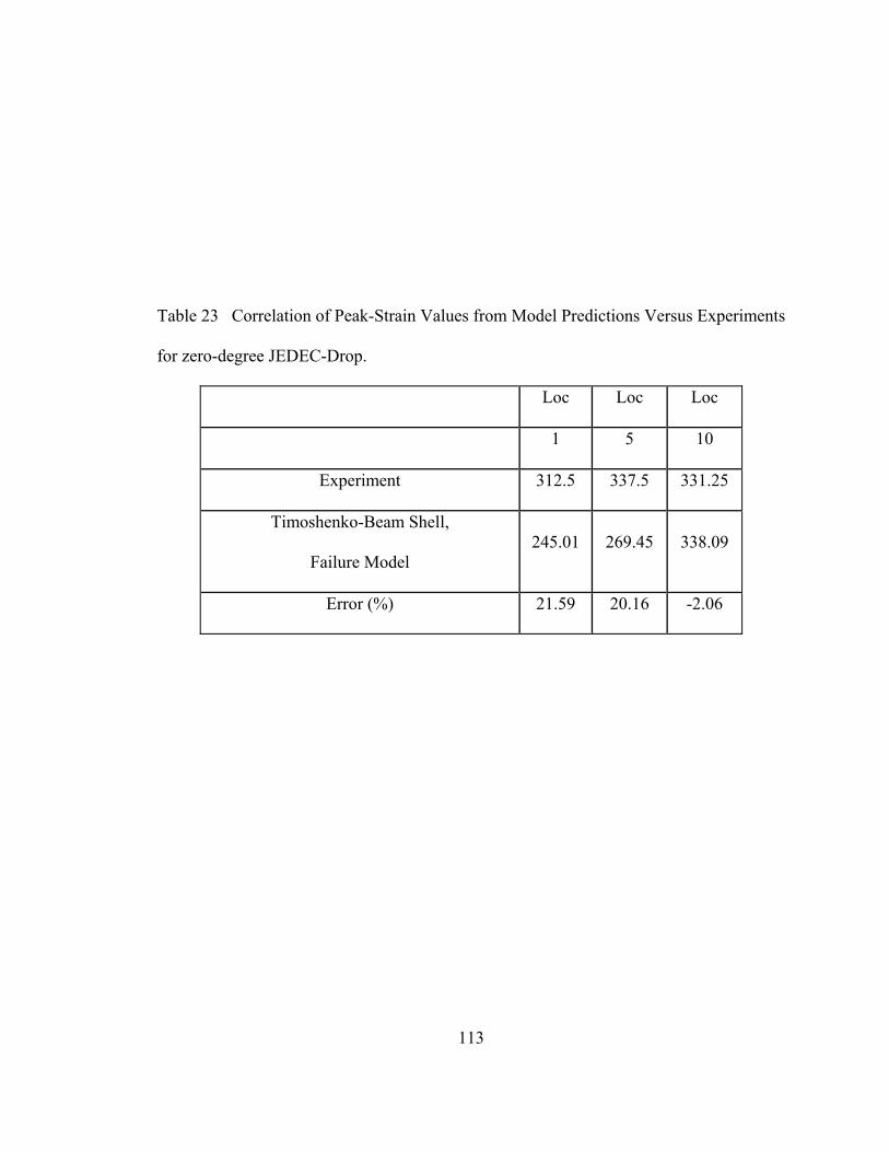
113
Table 23 Correlation of Peak-Strain Values from Model Predictions Versus Experiments
for zero-degree JEDEC-Drop.
Loc Loc Loc
1 5 10
Experiment 312.5 337.5 331.25
Timoshenko-Beam Shell,
Failure Model 245.01 269.45 338.09
Error (%) 21.59 20.16 -2.06

114
Global Model
Explicit Sub-Models
Global Model
Explicit Sub-Models
Figure 58 Explicit Sub-modeling technique employed at all component locations.
-0.0008
-0.0006
-0.0004
-0.0002
0
0.0002
0.0004
0.0006
0.0008
0 0.002 0.004 0.006Time (sec)
Rel
ativ
e D
ispla
cem
ent (
met
er)
Global Model
Explicit Sub-Model
Figure 59 Time History of the displacement at the boundary nodes of the global model
and the explicit sub-model.

115
Table 24 Correlation of Timoshenko-Beam Failure Model Predictions with Experimental
data for solder interconnect failure location for JEDEC Drop.

116
Table 25 Correlation of Timoshenko-Beam Failure Model Predictions with Experimental
data for solder interconnect failure location for Free Drop.

117
Table 26 Correlation of Explicit Cohesive Sub-Model Predictions with Experimental data
for solder interconnect failure location for Free Drop.
CSP Location
Experimental Location of Failure
Cohesive Zone Stress History at Failure Location
1
Failure LocationFailure Location
t = 2.1 ms
t = 6.0 mst = 4.5 ms
t = 3.3 mst = 2.1 ms
t = 6.0 mst = 4.5 ms
t = 3.3 ms
5
Failure LocationFailure Location
t = 2.7 ms
t = 5.1 mst = 4.2 ms
t = 3.0 mst = 2.7 ms
t = 5.1 mst = 4.2 ms
t = 3.0 ms
10
Failure LocationFailure Location
t = 2.4 ms
t = 6.0 mst = 4.5 ms
t = 3.0 mst = 2.4 ms
t = 6.0 mst = 4.5 ms
t = 3.0 ms

118
In addition, CSP locations 1, 7, 9, 10 exhibit dominant failure locations at different array
locations for the same drop orientation. Once the beams fail, they are deleted from the
array in the simulation. The location of the missing beams in Table 24 and Table 25 show
good correlation with location of failure from cross-sections. For some package location,
simulation indicates failure of multiple beams, which also correlates with the cross-
section results.
Figure 59 shows the excellent correlation between the displacement time history
at the boundary nodes of the global model and the corresponding explicit sub-model thus
ensuring that the results from the global model are accurately transferred on to the sub-
model. Table 26 shows the progressive deletion of the cohesive elements at the solder
joint-copper pad interface on the PCB side at various component locations once the
maximum value of the damage variable is reached. This prediction clearly shows the
susceptibility to failure of the IMC layer at the solder joint-copper pad interface subject to
drop impact. The cohesive elements located at the outer periphery of the interface
experience maximum stresses and are deleted first which is in accordance with the
observations generally seen during failure analysis of the failed samples in that crack
initiation generally starts from the outer boundary and progresses inward. Furthermore,
the maximum or the peak value of the Von Mises stress in the cohesive elements
predicted by the cohesive zone model approximately varies from 100 MPa to 280 MPa
depending on component location and also on where the element is located along the
solder joint-copper pad interface. The solder joint array pull experimental test carried out
high strain rates also shows the value of the failure stress at the point of interfacial failure

119
0
50
100
150
200
250
CSP # 3 CSP # 7 CSP # 9
Maximum Peak Strainin millistrainsNumber of Drops toFailure
Figure 60 Number of drop to failure as a function of maximum peak strain in the
cohesive element at different component locations for JEDEC Drop.
120
to be around 110-120 MPa [Darveaux et al. 2006] thus providing good correlation with
the model predictions. Figure 60 shows the correlation between the magnitude of the
peak transient strains in the cohesive elements obtained from simulation and the number
of drops to failure at different component locations obtained experimentally by carrying
out JEDEC drop. It can be seen that higher strains experienced by the cohesive elements
located at the IMC layer of the corner solder joints at different component locations
results in earlier failures of the packages due to solder interconnection fracture failure.

121
CHAPTER 6
SUMMARY AND CONCLUSIONS
In this research effort, the transient dynamic responses of the board level
assemblies subject to drop impact have been investigated to enable the prediction of
solder joint reliability under shock and vibration environments. Four explicit modeling
techniques have been investigated for modeling shock loading of printed circuit board
assemblies. The focus of the research effort was on modeling multiple scales from first-
level interconnects to assembly-level transient dynamics. Modeling techniques
investigated included smeared properties, Timoshenko-beam with Conventional Shell
Elements, Timoshenko-Beam with Continuum Shell Elements, and Explicit Sub-
modeling. This work extends the state-of-art, which presently focuses on prediction of
interconnect stresses based on assumptions of symmetry of geometry and boundary
conditions. In this research effort, modeling techniques have been developed to capture
system-level dynamics in addition to interconnect transient-stress and transient-strain
histories, without any assumption of assembly symmetry. The ability to eliminate
symmetry assumptions enables the modeling of asymmetric modes in addition to
symmetric modes. The model predictions have been correlated with experimental data
from high-speed video, high-speed image analysis and high-speed strain acquisition.
Model predictions shows excellent correlation with experimental data in terms of the

122
relative displacement and transient strain time histories. The various modeling
methodologies employed resulted in increased computational efficiency while
maintaining a good degree of accuracy. Model predictions also enabled the detection of
the location and mode of failure of the critical solder interconnections most susceptible to
failure when subject to drop impact.
Two failure prediction models namely the Timoshenko Beam Failure model and
the Cohesive Zone Failure model have also been incorporated to predict the location and
the mode of failures in the solder interconnections subject to drop impact respectively.
The Timoshenko Beam Failure model predicts the location of the most critical solder
interconnection susceptible to failure at the high strain rates experienced during drop. The
Cohesive Zone failure model, on the other hand, shows the progressive degradation and
failure of the cohesive elements located at the IMC layer leading to solder joint brittle
interfacial failure. These predictions have shown very good correlation with the
experimental drop tests and the observed failures modes observed by carrying out failure
analysis.

123
BIBLIOGRAPHY
Abaqus Documentation, Dynamic Failure Models, Abaqus Analysis User’s Manual,
Version 6.6, Section 18.2.8, 2006a.
Abaqus Documentation, Cohesive Elements, Abaqus Analysis User’s Manual,
Version 6.6, Section 26.5, 2006b.
Abaqus Documentation, Finite Elements and Rigid Bodies, Getting Started with
Abaqus Explicit: Keywords Version, Version 6.5, Section 4.1, 2005a.
Abaqus Documentation, Beam Element Overview, Abaqus Theory Manual, Version
6.5, Section 3.5.1, 2005b.
Abdul-Baqi, A., Schreurs, P. J. G., Geers, M. G. D., “Fatigue damage modeling in
solder interconnects using a cohesive zone approach”, International Journal of
Solids and Structures, Volume 42, pp. 927-942, 2005.

124
Bansal, A., Yoon, S., Mahadev, V., “Flexural Strength of BGA Solder Joints with
ENIG Substrate Finish using 4-Point Bend Test”, Proceedings of the SMTA Pan
Pacific Microelectronics Symposium, pp. 1-8, 2005.
Carroll, D., Zampino, M., Jones, K., “Bending Simulation of BGA SMT Assemblies
and Application to System Level Drop Simulation”, Proceedings of IPACK2005,
pp. 1-9, 2005.
Chai, T. C., Quek, S., Hnin, W. Y., Wong, E. H., “Drop Level Drop Test Reliability
of IC Packages”, Proceedings of the 55th Electronic Components and Technology
Conference, pp. 630-636, 2005.
Chong, D. Y. R., Ng, K., Tan, J. Y. N., Low, P. T. H., “Drop Impact Reliability
Testing for Lead-Free and Leaded Soldered IC Packages”, Proceedings of the 55th
Electronic Components and Technology Conference, pp. 622-629, 2005.
Clech., J-P., “Solder Reliability Solutions: a PC-based Design-for-reliability Tool”,
Proceedings of the Surface Mount International Conference, pp. 136-151, 1996.

125
Clech., J-P., “Flip-chip /CSP Assembly Reliability and Solder Volume Effects”,
Proceedings of the Surface Mount International Conference, pp. 315-324, 1998.
Date, M., Shoji, T., Fujiyoshi, M., Sato, K., Tu, K. N., “Impact Reliability of Solder
Joints”, Proceedings of the 54th Electronic Components and Technology
Conference, pp. 668-674, 2004.
Darveaux, R., Reichman, C., Islam, N., “Interface Failure in Lead Free Solder Joints”,
Electronic Components and Technology Conference, pp. 906-917, 2006.
Erich, R., Coyle, J. R., Wenger, G. M., Primavera, A., “Shear Testing and Failure
Mode Analysis for Evaluation of BGA Ball Attachment”, Proceedings of the
IEEE/CPMT International Electronics Manufacturing Technology Symposium,
pp. 16-22, 1999.
Ferracin, T., Landis, C. M., Delannay, F., Pardoen, T., “On the determination of the
cohesive zone properties of an adhesive layer from the analysis of the wedge-peel
test”, International Journal of Solids and Structures, Volume 40, pp. 2889-2904,
2003.
Harada, K., Baba, S., Wu, Q., Matsushima, H., Matsunaga, T., Uegai, Y., Kimura,
M., “Analysis of Solder Joint Fracture under Mechanical Bending Test”,
Electronic Components and Technology Conference, pp. 1731-1737, 2003.

126
Geng, P., “Dynamic Test and Modeling Methodology for BGA Solder Joint Shock
Reliability Evaluation”, Proceedings of the 55th Electronic Components and
Technology Conference, pp. 654-659, 2005.
Gu, J., Lim, C. T., Tay, A. A. Y., “Equivalent Solder Joint and Equivalent Layer
Models for the Simulation of Solder Column Failure under Drop Impact”,
Proceedings of the 6th Electronic Packaging Technology Conference, pp. 547-552,
2004.
Gu, J., Lim, C. T., Tay, A. A. Y., “Modeling of Solder Joint Failure due to PCB
Bending during Drop Impact”, Proceedings of the 6th Electronic Packaging
Technology Conference, pp. 678-683, 2004.
Gu, J., Lim, C. T., Tay, A. A. Y., “Simulation of Mechanical Response of Solder
Joints under Drop Impact Using Equivalent Layer Models”, Proceedings of the
55th Electronic Components and Technology Conference, pp. 522-529, 2005.
Hanabe, M., Canumalla, S., “Package to Board Interconnection Shear Strength
(PBISS) behavior at High Strain Rates Approaching Mechanical Drop”,
Proceedings of the 54th Electronic Components and Technology Conference, pp.
1263-1270, 2004.

127
Hanabe, M., Canumalla, S., Kujala, A., “ Enhancing Drop Test Efficacy for Product
Quality Improvement through Interconnection Shear Tests”, Proceedings of the
56th Electronic Components and Technology Conference, pp. 83-88, 2006.
Irving, S., Liu, Y., “Free Drop Test Simulation for Portable IC Package by Implicit
Transient Dynamics FEM”, Proceedings of the 54th Electronic Components and
Technology Conference, pp. 1062-1066, 2004.
JEDEC Standard IPC/JEDEC-9702, Monotonic Bend Characterization of Board-
Level interconnects, 2004.
JEDEC Solid State Technology Association, Board-Level Drop Test Method of
Components for Handheld Electronic Products, No. JESD22-B111, 2003.
Lall, P., Choudhary, P., Gupte, S., Suhling, J., “Health Monitoring for Damage
Initiation & Progression during Mechanical Shock in Electronic Assemblies”,
Proceedings of the 56th Electronic Components and Technology Conference, pp.
96-105, 2006.
Lall, P., Panchagade, D., Choudhary, P., Suhling, J., Gupte, S., “Failure-Envelope
Approach to Modeling Shock and Vibration Survivability of Electronic and
MEMS Packaging”, Proceedings of the 55th Electronic Components and
Technology Conference, pp. 522-529, 2005.

128
Lall, P., Panchagade, D., Liu, Y., Johnson, W., Suhling, J., “Models for Reliability
Prediction of Fine-Pitch BGAs and CSPs in Shock and Drop Impact”,
Proceedings of the 54th Electronic Components and Technology Conference, pp.
1296-1303, 2004.
Lim, C. T., Ang, C. W., Tan, L. B., Seah, S. K. W., Wong, E.H., “Drop Impact survey
of Electronic Products”, Proceedings of the 53rd Electronic Components and
Technology Conference, pp. 113-120, 2003.
Lim, C. T., Low, Y. J., “Investigating the Drop Impact of Portable Electronic
Products”, Proceedings of the 52nd Electronic Components and Technology
Conference, pp. 1270-1274, 2002.
Luan, J., Tee, T. Y., “Novel Board Level Drop Test Simulation using Implicit
Transient Analysis with Input-G Method”, Proceedings of the 6th Electronic
Packaging Technology Conference, pp. 671-677, 2004.
Marjakami, P., Mattila, T., Kivilahti, J., “Finite Element Analysis of Lead-Free Drop
Test Boards”, Proceedings of the 55th Electronic Components and Technology
Conference, pp. 462-466, 2005.

129
Mishiro, K., Ishikawa, S., Abe, Mitsunori., Kumai, T., Higashiguchi, Y., Tsubone, K.,
“Effect of the drop impact on BGA/CSP package reliability”, Transactions on
Microelectronics Reliability, Vol. 42, pp. 77-82, 2002.
Needleman, A., “A Continuum Model for Void Nucleation by Inclusion Debonding”,
Journal of Applied Mechanics, Volume 54, pp. 525-531, 1987.
Needleman, A., “An analysis of decohesion along an imperfect interface”,
International Journal of Fracture, Volume 42, pp. 21-40, 1990.
Newman, K., “BGA Brittle Fracture - Alternative Solder Joint Integrity Test
Methods”, Electronic Components and Technology Conference, pp. 1194-1201,
2005.
Ong, Y. C., Shim, V.P.W., Chai, T.C., Lim, C.T., “Comparison of Mechanical
Response of PCBs Subjected to Product-Level and Board-Level Drop Impact
Tests”, Proceedings of the 5th Electronic Packaging Technology Conference, pp.
223-227, 2003.
Ong, K. C., Tan, V. B. C., Lim, C. T., Wong, E. H., Zhang, X. W., “Dynamic
Materials Testing and Modeling of Solder Interconnects”, Proceedings of the 54th
Electronic Components and Technology Conference, pp. 1075-1079, 2005.

130
Pang, J. H. L., Che, F. X., “ Drop Impact Analysis of Sn-Ag-Cu Solder Joints Using
Dynamic High-Strain Rate Plastic Strain as the Impact Damage Driving Force”,
Proceedings of the 56th Electronic Components and Technology Conference, pp.
49-54, 2006.
Pang, J. H. L., Che, F. X., Low, T. H., “Vibration Fatigue Analysis For FCOB Solder
Joints”, Proceedings of the 54th Electronic Components and Technology
Conference, pp. 1055-1061, 2004.
Pitarressi, J., Roggeman, B., Chaparala, S., “Mechanical Shock Testing and Modeling
of PC Motherboards”, Proceedings of the 54th Electronic Components and
Technology Conference, pp. 1047-1054, 2004.
Ren, W., Wang, J., “Shell-Based Simplified Electronic Package Model Development
and Its Application for Reliability Analysis”, Proceedings of the 5th Electronic
Packaging Technology Conference, pp. 217-222, 2003.
Ren, W., Wang, J., Reinikainen, T., “Application of ABAQUS/Explicit Submodeling
Technique in Drop Simulation of System Assembly”, Proceedings of the 6th
Electronic Packaging Technology Conference, pp. 541-546, 2004.
Scheider, I., “Cohesive model for crack propagation analyses of structures with
elastic–plastic material behavior”, GKSS research center, Geesthacht, 2001.

131
Schwalbe, K.-H., Cornec, A., “Modeling crack growth using local process zones”’
Technical report, GKSS research centre, Geesthacht, 1994.
Shah, K. R., Mello M., “Ball Grid Array Solder Joint Failure Envelope Development
for Dynamic Loading”, Proceedings of the 54th Electronic Components and
Technology Conference, pp. 1067-1074, 2004.
Shetty, S., Reinikainen, T., “Three- and Four-Point Bend Testing for Electronic
Packages”, Transactions of the ASME, pp. 556-561, 2003.
Syed, A., “Predicting Solder Joint Reliability for Thermal, Power, & Bend Cycle
within 25% Accuracy”, Proceedings of the 51st Electronic Components and
Technology Conference, pp. 522-529, 2001.
Syed, A., Kim, S. M., Lin, W., Khim, J. Y., Song, E. S., Shin, J. H., Panczak, T., “A
Methodology for Dropp Performance Prediction and Application for Design
Optimization of Chip Scale Packages”, Proceedings of the 55th Electronic
Components and Technology Conference, pp. 472-479, 2005.
Tan, V. B. C., Tong, M. X., Lim, K. M., Lim, C. T., “Finite Element Modeling of
Electronic Packages Subjected to Drop Impact”, IEEE Transactions on
Components and Packaging Technologies, pp. 111-222, 2005.

132
Tee, T. Y., Luan, J., Ng, H. S., “Development and Application of Innovational Drop
Impact Modeling Techniques”, Proceedings of the 55th Electronic Components
and Technology Conference, pp. 615-623, 2005.
Tee, Y. T., Luan, J., Pek, E., Lim, C. T., Zhong, Z., “Advanced Experimental and
Simulation Techniques for Analysis of Dynamic Responses during Drop Impact”,
Proceedings of the 54th Electronic Components and Technology Conference, pp.
1088-1094, 2004.
Tee, T. Y., Ng, H. S., Lim, C.T., Pek, E., “Drop Impact and Impact Life Prediction
Model for QFN Packages”, Journal of SMT, Volume 16, Issue 3, pp. 31-39, 2003.
Tee, T. Y., Luan, J., Pek, E., Lim, C. T., Zhong, Z, “Novel Numerical and
Experimental Analysis of Dynamic Responses under Board Level Drop Test”,
Proceedings of the 5th International Conference on Thermal and Mechanical
Simulation and Experiments in Micro-electronics and Micro-Systems, pp. 133-
140, 2004.
Towashiraporn, P., Subbarayan, G., Desai, C. S., “A hybrid model for
computationally efficient fatigue fracture simulations at microelectronic assembly
interfaces”, International Journal of Solids and Structures, Volume 42, pp. 4468-
4483, 2005.

133
Towashiraporn, P., Xie, C., “Cohesive Modeling of Solder Interconnect Failure in
Board Level Drop Test”, Proceedings of the ITHERM, pp. 817-825, 2006.
Tvergaard, V., Hutchinson, J.W., The relation between crack growth resistance and
fracture process parameters in elastic-plastic solids, Journal of the Mechanics and
Physics of Solids, Volume 40, pp. 1337–1397, 1992.
Wang, Y.Q., Low, K.H., Che, F.X., Pang, H.L.J., Yeo, S.P., “Modeling and
Simulation of Printed Circuit Board Drop Test”, Proceedings of the 5th Electronic
Packaging Technology Conference, pp. 263-268, 2003.
Wang, Y. Y., Wang, F., Chai, T. C., “Finite Element Modeling of CSP Package
Subjected to Board Level Drop Test”, Proceedings of the 6th Electronic Packaging
Technology Conference, pp. 684-688, 2004.
Wong, E. H., Lim, C. T., Field, J. E., Tan, V. B. C., Shim, V. P. W., Lim, K. M.,
Seah, S. K. W., “Tackling the Drop Impact Reliability of Electronic Packaging”,
Proceedings of IPACK05 International Electronic Packaging Technical
Conference and Exhibition, pp. 1-7, 2005.
Wong, E. H., Lim, K. M., Lee, N., Seah, S., Hoe, C., Wang, J., “Drop Impact Test –
Mechanics & Physics of Failure”, Proceedings of the 4th Electronic Packaging
Technology Conference, pp. 327-333, 2002.

134
Wong, E. H., Rajoo, R., Mai, Y. W., Seah, S. K. W., Tsai, K. T., Yap, L. M., “Drop
Impact: Fundamentals & Impact Characteristics of Solder Joints”, Proceedings of
the 55th Electronic Components and Technology Conference, pp. 1202-1209,
2005.
Wu, J., Song, G., Yeh, C., Wyatt, K., “Drop/Impact Simulation and Test Validation
of Telecommunication Products”, Proceedings of the InterSociety Conference on
Thermal Phenomena, pp. 330-336, 1998.
Xie, D., Arra, M., Yi, S., Rooney, D., “Solder Joint Behavior of Area Array Packages
in Board Level Drop for Handheld Devices”, Proceedings of the 53rd Electronic
Components and Technology Conference, pp. 130-135, 2003.
Yu, Q., Kikuchi, H., Ikeda, S., Shiratori, M., Kakino, M., Fujiwara N., “Dynamic
Behavior of Electronics Package and Impact Reliability of BGA Solder Joints”,
Proceedings of the Inter Society Conference on Thermal Phenomena, pp. 953-
960, 2002.
Zahn, B. A., “Solder Joint Fatigue Life Model Methodology for 63Sn37Pb and
95.5Sn4Ag0.5Cu Materials”, Proceedings of the 53th Electronic Components and
Technology Conference, pp. 83-94, 2003.

135
Zhao, J., Garner, L. J., “Mechanical Modeling and Analysis of Board Level Drop Test
of Electronic Package”, Proceedings of the 56th Electronic Components and
Technology Conference, pp. 547-553, 2006.
Zhu, L., “Modeling Technique for Reliability Assessment of Portable Electronic
Product Subjected to Drop Impact Loads”, Proceedings of the 53rd Electronic
Components and Technology Conference, pp. 100-104, 2003.
Zhu, L., Marcinkiewicz, W., “Drop Impact Reliability Analysis of CSP Packages at
Board and Product System Levels Through Modeling Approaches”, Proceedings
of the Inter Society Conference on Thermal Phenomena, pp. 296-303, 2004.
Zhu, J., Quander, S., Reinikainen, T., “Global/Local Modeling for PWB Mechanical
Loading”, Proceedings of the 51st Electronic Components and Technology
Conference, pp. 130-135, 2001.